Thermal and chemical vapor deposition of Si nanowires: Shape
13
Thermal and chemical vapor deposition of Si nanowires: Shape control, dispersion, and electrical properties A. Colli, a A. Fasoli, P. Beecher, P. Servati, b S. Pisana, Y. Fu, A. J. Flewitt, W. I. Milne, and J. Robertson Department of Engineering, University of Cambridge, Cambridge CB3 0FA, United Kingdom C. Ducati Department of Materials Science and Metallurgy, University of Cambridge, Cambridge CB3 6GF, United Kingdom S. De Franceschi Laboratoire de Transport Electronique Quantique et Supraconductivité, CEA-Grenoble, 38054 Grenoble cedex 9, France S. Hofmann and A. C. Ferrari c Department of Engineering, University of Cambridge, Cambridge CB3 0FA, United Kingdom Received 21 March 2007; accepted 14 June 2007; published online 6 August 2007 We investigate and compare complementary approaches to SiNW production in terms of yield, morphology control, and electrical properties. Vapor-phase techniques are considered, including chemical vapor deposition with or without the assistance of a plasma and thermal evaporation. We report Au-catalyzed nucleation of SiNWs at temperatures as low as 300 ° C using SiH 4 as precursor. We get yields up to several milligrams by metal-free condensation of SiO powders. For all processes, we control the final nanostructure morphology. We then report concentrated and stable dispersions of SiNWs in solvents compatible with semiconducting organic polymers. Finally, we investigate the electrical response of intrinsic SiNWs grown by different methods. All our SiNWs exhibit p-type behavior and comparable performance, though in some cases ambipolar devices are observed. Thus, processing and morphology, rather than the growth technique, are key to achieve optimal samples for applications. © 2007 American Institute of Physics. DOI: 10.1063/1.2764050 I. INTRODUCTION The bottom-up synthesis of one-dimensional 1D semi- conducting nanostructures has attracted increasing interest in recent years both for fundamental physics and for potential device applications. 1–8 On the one hand, the capability to synthesize nanoscale building blocks without the need of ex- pensive and time-consuming lithography techniques offers key opportunities for high-integration nanoelectronics. Re- search is therefore heading towards the realization of single- nanowire NW or crossed-NW devices with the aim of in- tegrating a large number of active components into a rational geometry. 3–5,9,10 On the other hand, applications are envis- aged where nanostructured materials do not require indi- vidual manipulation but are assembled as bulk, while indi- vidually retaining their nanoscale properties such as quantum confinement or large surface-to-volume ratio. 6–8,11,12 As a consequence, several synthesis approaches are being devel- oped to match the specific requirements of different possible applications. Bulk production of nanocrystals both in solution 13,14 or from the vapor phase 15,16 for post-growth manipulation has received as much attention as the selective and oriented growth of NWs directly into devices. 17,18 Si nanowires SiNWs are particularly relevant due to the central role of Si in the semiconductor industry. Deposi- tion techniques for SiNWs include laser ablation 16,19 high temperature thermal evaporation, 20–22 molecular beam epi- taxy MBE, 23 chemical vapor deposition CVD, 24–26 and plasma-enhanced CVD PECVD. 27 CVD is probably the most investigated synthesis tech- nique for SiNWs. 24–26 Generally, a metal nanoparticle is re- quired to favor selective decomposition of the precursor gas and the consequent nucleation of substrate-bound 1D nanostructures. 28,29 By patterning the catalyst on oriented crystalline substrates, defined and oriented arrays of SiNWs have been fabricated. 26 This highlights the potential of the CVD approach for the realization of bottom-up nanoscale devices, where active components are no longer manufac- tured but grown from point to point in a controlled fashion. In this framework, however, the fabrication step involving NW synthesis must be compatible with the whole process flow. This implies, for example, that the NW growth tem- perature must be low enough to ensure compatibility with the final device substrate. Efforts are therefore addressed to fully understand the physics and chemistry behind the growth of semiconductor NWs and to explore the lowest growth tem- perature achievable by the metal-assisted mechanism. 30–34 Bulk production is emerging as an alternative approach for the fabrication and assembly of NWs in large quantities. Several growth strategies have been proposed to achieve large-scale SiNW growth, most of them still requiring the presence of a metal catalyst to promote 1D nucleation. 16,19–22 a Electronic mail: [email protected] b Present address: University of British Columbia, 2332 Main Mall, Vancou- ver, BC V6T 1Z4, Canada. c Electronic mail: [email protected] JOURNAL OF APPLIED PHYSICS 102, 034302 2007 0021-8979/2007/1023/034302/13/$23.00 © 2007 American Institute of Physics 102, 034302-1 Downloaded 18 Dec 2007 to 129.169.174.178. Redistribution subject to AIP license or copyright; see http://jap.aip.org/jap/copyright.jsp
Transcript of Thermal and chemical vapor deposition of Si nanowires: Shape

Thermal and chemical vapor deposition of Si nanowires:Shape control, dispersion, and electrical properties
A. Colli,a� A. Fasoli, P. Beecher, P. Servati,b� S. Pisana, Y. Fu, A. J. Flewitt, W. I. Milne,and J. RobertsonDepartment of Engineering, University of Cambridge, Cambridge CB3 0FA, United Kingdom
C. DucatiDepartment of Materials Science and Metallurgy, University of Cambridge, Cambridge CB3 6GF,United Kingdom
S. De FranceschiLaboratoire de Transport Electronique Quantique et Supraconductivité, CEA-Grenoble,38054 Grenoble cedex 9, France
S. Hofmann and A. C. Ferraric�
Department of Engineering, University of Cambridge, Cambridge CB3 0FA, United Kingdom
�Received 21 March 2007; accepted 14 June 2007; published online 6 August 2007�
We investigate and compare complementary approaches to SiNW production in terms of yield,morphology control, and electrical properties. Vapor-phase techniques are considered, includingchemical vapor deposition �with or without the assistance of a plasma� and thermal evaporation. Wereport Au-catalyzed nucleation of SiNWs at temperatures as low as 300 °C using SiH4 as precursor.We get yields up to several milligrams by metal-free condensation of SiO powders. For allprocesses, we control the final nanostructure morphology. We then report concentrated and stabledispersions of SiNWs in solvents compatible with semiconducting organic polymers. Finally, weinvestigate the electrical response of intrinsic SiNWs grown by different methods. All our SiNWsexhibit p-type behavior and comparable performance, though in some cases ambipolar devices areobserved. Thus, processing and morphology, rather than the growth technique, are key to achieveoptimal samples for applications. © 2007 American Institute of Physics. �DOI: 10.1063/1.2764050�
I. INTRODUCTION
The bottom-up synthesis of one-dimensional �1D� semi-conducting nanostructures has attracted increasing interest inrecent years both for fundamental physics and for potentialdevice applications.1–8 On the one hand, the capability tosynthesize nanoscale building blocks without the need of ex-pensive and time-consuming lithography techniques offerskey opportunities for high-integration nanoelectronics. Re-search is therefore heading towards the realization of single-nanowire �NW� or crossed-NW devices with the aim of in-tegrating a large number of active components into a rationalgeometry.3–5,9,10 On the other hand, applications are envis-aged where nanostructured materials do not require indi-vidual manipulation but are assembled as bulk, while indi-vidually retaining their nanoscale properties such as quantumconfinement or large surface-to-volume ratio.6–8,11,12 As aconsequence, several synthesis approaches are being devel-oped to match the specific requirements of different possibleapplications. Bulk production of nanocrystals �both insolution13,14 or from the vapor phase15,16� for post-growthmanipulation has received as much attention as the selectiveand oriented growth of NWs directly into devices.17,18
Si nanowires �SiNWs� are particularly relevant due to
the central role of Si in the semiconductor industry. Deposi-tion techniques for SiNWs include laser ablation16,19 hightemperature thermal evaporation,20–22 molecular beam epi-taxy �MBE�,23 chemical vapor deposition �CVD�,24–26 andplasma-enhanced CVD �PECVD�.27
CVD is probably the most investigated synthesis tech-nique for SiNWs.24–26 Generally, a metal nanoparticle is re-quired to favor selective decomposition of the precursor gasand the consequent nucleation of substrate-bound 1Dnanostructures.28,29 By patterning the catalyst on orientedcrystalline substrates, defined and oriented arrays of SiNWshave been fabricated.26 This highlights the potential of theCVD approach for the realization of bottom-up nanoscaledevices, where active components are no longer manufac-tured but grown from point to point in a controlled fashion.In this framework, however, the fabrication step involvingNW synthesis must be compatible with the whole processflow. This implies, for example, that the NW growth tem-perature must be low enough to ensure compatibility with thefinal device substrate. Efforts are therefore addressed to fullyunderstand the physics and chemistry behind the growth ofsemiconductor NWs and to explore the lowest growth tem-perature achievable by the metal-assisted mechanism.30–34
Bulk production is emerging as an alternative approachfor the fabrication and assembly of NWs in large quantities.Several growth strategies have been proposed to achievelarge-scale SiNW growth, most of them still requiring thepresence of a metal catalyst to promote 1D nucleation.16,19–22
a�Electronic mail: [email protected]�Present address: University of British Columbia, 2332 Main Mall, Vancou-
ver, BC V6T 1Z4, Canada.c�Electronic mail: [email protected]
JOURNAL OF APPLIED PHYSICS 102, 034302 �2007�
0021-8979/2007/102�3�/034302/13/$23.00 © 2007 American Institute of Physics102, 034302-1
Downloaded 18 Dec 2007 to 129.169.174.178. Redistribution subject to AIP license or copyright; see http://jap.aip.org/jap/copyright.jsp
With process temperatures usually exceeding 1000 °C, Au,Fe, Ga, and Sn are mixed to the Si precursor vapor either bythermal evaporation or laser ablation. NWs are collectedfrom the furnace reactor in form of woolenlike bundles.19,20
There is a need, however, to avoid the metal contamina-tion potentially arising from the residual catalyst particles.Removing the catalyst postgrowth may require complex andexpensive purification treatments.35 The so-called oxide-assisted growth �OAG� method provides a viable alternativefor metal-free bulk production of SiNWs.15,36 Reference 37reported the production of milligrams of SiNWs by thermalevaporation of SiO. It was suggested that SiO triggers theself-assembly of SiNWs, based on the observation that pureSi or pure SiO2 as precursor materials gave negligibleyield.38 Indeed, a SiOx �x�1� thin film ��1.3 nm� was alsofound to promote the metal-free nucleation of InAs NWs,39,40
although it was not clear in this case if this process could beexplained by the oxide-assisted growth model of Ref. 15. Todate, evaporation of SiO �or mixtures of Si and SiO2� stillremains the most flexible and reliable approach to metal-freeSiNW synthesis.37,38,41 This method, however, has limita-tions for the shape control and uniformity of the resultingnanostructures. Thin and crystalline SiNWs are oftencoupled with partially or fully oxidized structures, resultingin crystalline Si spheres connected into chains by SiO2
bridges of variable length.42–44 References 42 and 43 linkedsuch shape variation to the local condensation temperature.They proposed a two-step growth dynamics where SiNWformation is followed by thermal oxidation of the crystallineSi cores. This was motivated by the observation of an in-creasing fraction of oxidized nanochains in the hotter regionsof the furnace tube.42 Shape separation of as-grown NWbundles requires further processing. Ideally one should engi-neer and optimize the synthesis to achieve 100% yield of thedesired nanostructure morphology.
Thermal evaporation in an inert gas flow �commonlycalled vapor transport� is suitable for bulk production of sev-eral nanomaterials.15,45,46 The main advantages of vaportransport are its versatility, the use of a relatively cheap ex-perimental setup, and the fact that NW bundles of differentmaterials can be easily synthesized without the need of po-tentially dangerous precursor gases, such as SiH4. On theother hand, the high temperatures involved in the process dolimit the substrate selection. NWs prepared by this techniqueare suitable for postgrowth processing, typically via disper-sion in solution. Yet, very few studies have so far focused onSiNW suspensions,47–50 despite the fact that this is one of themain research topics in the carbon nanotubecommunity.35,51–53 In most cases, solution processing was in-vestigated just as a simple step toward dispersion of indi-vidual, as-grown NWs on solid substrates for transmissionelectron microscopy �TEM� or electrical characterization.3,21
However, many emerging applications �for example, hybridinorganic/organic composites54,55� require handling of high-density suspensions of NWs or nanocrystals, together withcontrolling on demand the chemical properties of the result-ing solution.
A key step to evaluate the NW suitability for applica-tions is the assessment of their electrical properties. It is
sometimes claimed that the use of SiNWs would result intransistor performances well above existing technologies, interms of mobility, trans-conductance, on/off ratio, etc.8,18,56
However, the reported values for SiNW hole mobility �ex-tracted from the transfer subthreshold slope and using asimple cylindrical model to estimate the NW capacitance�are so far widely scattered from�10 to 1350 cm2/V s.2,8,18,41,56 Also, it is difficult to pre-cisely estimate the doping concentration in NW channels.Many report SiNWs lightly or heavily doped.57–59 However,not many investigations focus on nominally intrinsicNWs.57,60,61 Also, a variety of different metals have beentested to contact SiNWs, such as Al/Au, Ni, Ti/Al, Ti/Au,and Cr/Au,3,56,57,60–62 and different annealing or passivationprotocols have been implemented.3,56,60–62 Because of this, adirect comparison of reports on electrical properties, evenwhen the same growth technique is utilized, is difficult. In-deed, scattered values for basic transistor parameters havebeen presented in literature for nominally equivalent SiNWchannels �see, for example, the properties review in Ref. 62�.
Thus, in this paper we perform an extensive character-ization and comparison of SiNWs grown by different tech-niques. We demonstrate selective synthesis of NWs andnanocones �NCs� down to 300 °C by CVD and PECVD, andassess the effect of several growth parameters in such lowtemperature nucleation regime. We also report the productionof bulk quantities of SiNWs by thermal evaporation, withand without the use of a metal catalyst. We show how toachieve shape control in oxide-assisted growth and stableSiNW dispersions in different solvents. Finally, we comparethe electrical properties of all types of SiNWs by using thesame device geometry and fabrication process. In particular,we focus on intrinsic SiNWs and observe preferential hole-accumulation behavior, though ambipolar field-effect transis-tors �FETs� are also obtained. Device response and perfor-mance appear to be dominated neither by the particularsynthesis process nor by the use of a metal catalyst.
II. EXPERIMENT
Both metal-seeded and metal-free growth of SiNWs areinvestigated. A quartz cylinder 4 cm in length and 5 cm indiameter acts as support for metal-free NW condensation.This allows easy unloading and collection of the as-grownmaterial. For metal-assisted growth, commercial Si sub-strates are coated and patterned with thin Au layers�0.5 nm�.27 Au is deposited by evaporating the precursormetal �99.99%� from a ceramic boat in a standard evaporatorat a base pressure below 10−6 mbar. The thickness of the Aulayer is determined by an in situ quartz crystal.
Low temperature, catalytic �PE�CVD growth is per-formed in an Oxford Instruments �P reactor, at a base pres-sure of 1�10−6 mbar. Au-coated Si substrates are heated to300 °C, as monitored by a thermocouple in direct contactwith the substrate surface. Then, pure SiH4 or H2-dilutedSiH4 is admitted with various flow rates. The total pressure isvaried between 200 mTorr and 10 Torr. A 13.6 MHz rfpower �5–30 W� is used to create a plasma, when needed.
High temperature, metal-assisted growth of SiNWs are
034302-2 Colli et al. J. Appl. Phys. 102, 034302 �2007�
Downloaded 18 Dec 2007 to 129.169.174.178. Redistribution subject to AIP license or copyright; see http://jap.aip.org/jap/copyright.jsp

studied by means of a thermal evaporation process in a fur-nace, at a base pressure of �10−3 mbar. Pure Si powders areplaced in an alumina boat and heated up to 1150–1250 °C.The Si vapor is carried downstream by a 100 SCCM �cubiccentimeter per minute at standard temperature and pressure�Ar flow and condenses along the colder regions�750–850 °C� of the furnace tube where the Au-coated sub-strates are placed. The Ar pressure is set to 100 mbars duringgrowth and 1 bar during the temperature ramps, to providepressure-based growth interruptions and avoid non steady-state effects.45 For oxide-assisted growth, SiO powders areevaporated at 1400 °C in an alumina tube, in the presence ofa 50 SCCM Ar flow �400–800 mbars�. The SiO vapor isfound to condense sharply in form of NW bundles at 950 °C.
For simplicity, in this paper we will refer to type I whenreporting Au-assisted SiNWs synthesized in a vacuum CVDreactor using SiH4 as precursor gas, type II to Au-assistedSiNWs grown by thermal evaporation of Si powders, andtype III to SiNW deposition by oxide-assisted metal-freegrowth performed in the same furnace as type II.
Au-coated quartz substrates are characterized by UV-visible absorption spectroscopy �Perkin Elmer Lambda 950spectrophotometer�. As-produced NWs are characterized byfield-emission scanning electron microscopy �FESEM�,TEM, and x-ray diffraction �XRD�. Three-terminal FETs arefabricated by dispersing SiNWs on a 200-nm-thick SiO2
layer thermally grown on a degenerate p-doped Si wafer,used as backgate. Source and drain contacts are defined bye-beam or x-ray lithography. After a short etching in bufferedHF to remove the NW oxide shell, interdigitated Ti/Al con-tacts �20/90 nm� are deposited by e-beam evaporation. Nocontact annealing is performed to avoid any further treatmentof as-grown SiNWs.
III. NANOWIRE GROWTH
A. Substrate preparation
Au thin films dewet at elevated temperatures��300 °C� forming a distribution of isolated catalystnanoparticles.63,64 Dewetting initiates at grain boundaries andedges through surface diffusion, and the metal can remaincrystalline.64 The film restructuring and the final shape of thecatalyst islands are a result of surface and interface energyminimization. The optical absorption of small metal clustersis strongly size and geometry dependent.63,65,66 The surfaceplasmon of colloidal gold lies in the visible region,63,66
which allows the restructuring of the Au film to be monitoredby UV-visible spectroscopy.
Figure 1 shows the adsorption spectra of an as-evaporated 0.5-nm-thick Au film on quartz, as well as of0.5-nm-thick Au annealed at 300 and 500 °C in vacuum. Theabsorption spectrum of 20 nm Au colloids dispersed onquartz is plotted for comparison. The as-evaporated Au filmshows a broad peak centered around 550 nm, which clearlyblueshifts to 526 nm upon annealing at 300 °C. The SEManalysis of patterned Au films on SiO2 annealed at 300 °C�Fig. 1, inset� indicates that arrays of quasispherical nanopar-ticles, 10–30 nm in diameter, form on the surface.
Early models correlated the absorption resonance shift tothe area fraction of the surface covered by metalnanoclusters,65 and consistently predicted a blueshift when athin film splits into isolated nanoparticles. Further studies,however, pointed out that quantitative predictions for the pre-cise position of the resonant frequency and the width of theresonance peak are challenging, since they are functions ofparticle size, shape, and interaction effects among denselyarrayed nanoparticles.63,66,67 From Fig. 1, we can infer thatrestructuring of the as-evaporated Au film already occurs at300 °C. This is a critical point, because a low, substrate-compatible NW growth temperature would be less appealingif a high temperature annealing was required beforehand foreffective catalyst preparation. Interestingly, annealing at500 °C leads to a small redshift and broadening compared tothe 300 °C sample. It is known that increasing the annealingtemperature leads to sintering and coalescence of nanopar-ticles, resulting in larger particle size at the expense of par-ticle density.63 Additional parameters can significantly affectthe formation of efficient catalyst nanoparticles for carbonnanotube �CNT� or NW growth, such as annealingatmosphere,68 roughness/morphology of the substrate,69 orplasma treatments with reactive gas species �see Sec. III B,Refs. 70 and 71�.
B. Catalytic CVD growth „type-I…
Au has been widely used to promote CVD SiNWgrowth.24–27 Its popularity comes essentially from two mer-its: �a� it does not oxidize in air or oxygen-rich atmospheres,and �b� it forms a liquid Au–Si eutectic at a relatively lowtemperature �363 °C�.72 It is often assumed that, accordingto the vapor-liquid-solid �VLS� model,28,29 NW formationoccurs when a catalyst droplet becomes supersaturated withthe NW precursor. This then precipitates from the solid-liquid interface to form a crystalline wire or tube.28,29 Themetal particle size determines the final diameter and is usu-ally found at the tip of the NW. In principle, the lowestpossible growth temperature allowed by the VLS is the melt-
FIG. 1. Optical absorption spectra for 0.5-nm-thick Au layers on quartz. Anabsorption spectrum for Au colloids 20 nm in diameter is shown as refer-ence. �Inset� SEM micrograph of a patterned Au layer on SiO2 annealed at300 °C, showing the bright contrast due to Au nanoparticles. Scale bar:100 nm.
034302-3 Colli et al. J. Appl. Phys. 102, 034302 �2007�
Downloaded 18 Dec 2007 to 129.169.174.178. Redistribution subject to AIP license or copyright; see http://jap.aip.org/jap/copyright.jsp
ing temperature of the catalyst particle. Accordingly, SiNWsgrowth in the 365–450 °C range is generally considered“low-temperature synthesis.”25,27,73 However, the meltingpoint of Si–Au eutectic nanoparticles may be lower than thevalue reported in bulk phase diagrams. It has been pointedout that size, precursor saturation, and substrate effects couldsignificantly shift the catalyst melting temperature 74,75 Infact, the VLS mechanism was invoked to explain NWgrowth for Si �Ref. 24� and Ge �Ref. 76� slightly below theAu–Si or Au–Ge eutectic temperature.24,76 On the otherhand, there is considerable evidence that NW nucleation canalso occur with a solid catalyst.31,32,77,78 Indeed, Ref. 31showed that the growth of InAs NWs is hindered as soon asthe temperature exceeds the predicted melting point of Au–In. Here we find a combination of growth parameters allow-ing SiNW synthesis at 300 °C both by CVD and PECVD.Since such low-temperature regime widens the availablerange of compatible substrates �e.g., plastic materials�, wechoose 300 °C as the growth temperature for our CVD ex-periments. A relatively low temperature can also minimizeundesirable effects such as catalyst diffusion or migrationduring NW growth.60,79
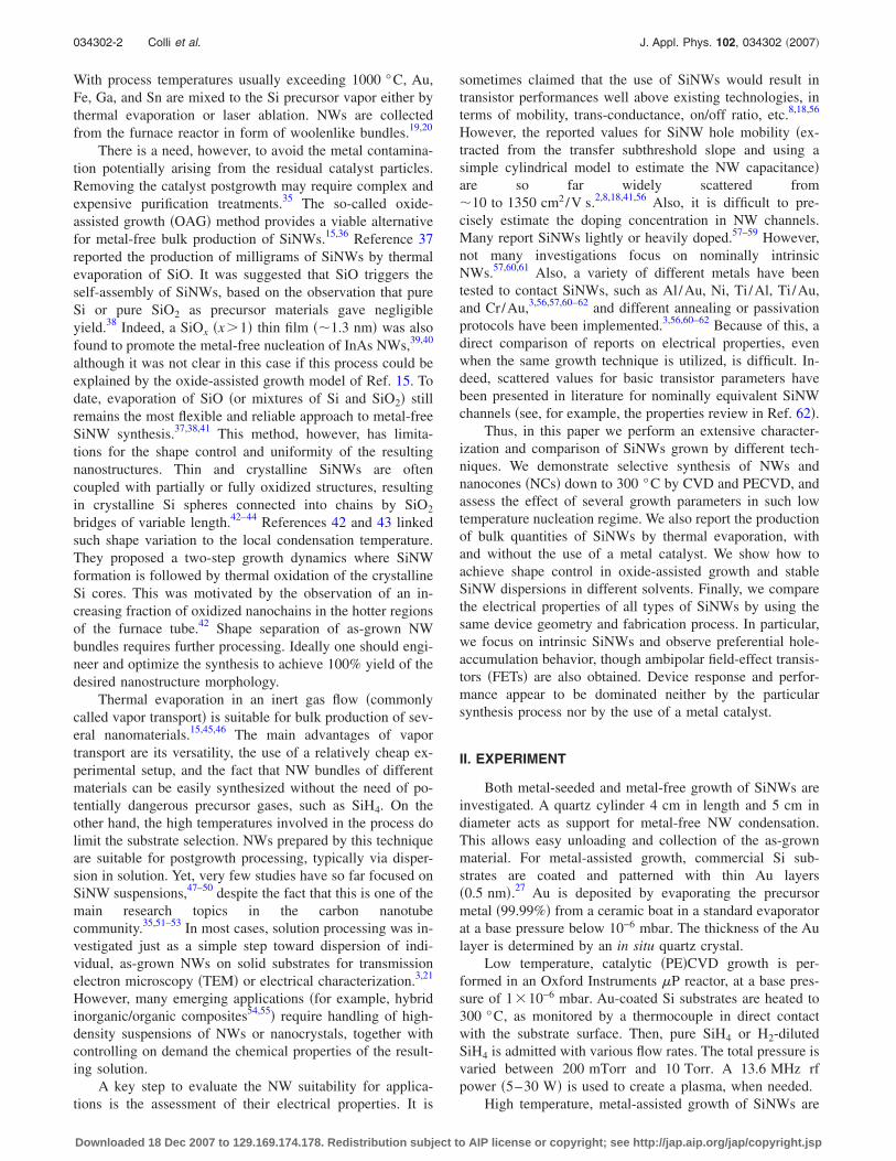
For thermal CVD, pure SiH4 is used. Figures 2�a� and2�b� show SiNWs grown with SiH4 pressures of 1 and10 Torr, respectively. Straight and thin �10–20 nm� SiNWsarise from Au-coated areas, and their length and density in-crease with increasing SiH4 pressure. No wires are found forSiH4 pressures below 1 Torr, but only unshaped Si structureson the catalyst layer. At 600 °C, however, SiNW growth wasreported inside a transmission electron microscope for pre-cursor gas pressures as low as 10−5 Torr.79 This would sug-gest that temperature and pressure are critically related inpromoting 1D crystallization during CVD growth of SiNWs.The reaction dynamics changes dramatically in the presenceof a plasma. At 10 Torr no plasma is ignited. At 3 Torr �Fig.2�c��, with low plasma power �10 W�, we observe relativelythick and tapered SiNWs �100–300 nm�, up to tens of mi-crons in length. Thus, for similar SiH4 pressures, a greatenhancement of the Au-promoted elongation rate is observedfor PECVD compared to thermal CVD.
Representative TEM micrographs of thermally grownSiNWs are shown in Figs. 3�a� and 3�b�. Thermal CVDyields thin ��10 nm� crystalline NWs uniform in diameter.The 1–2 nm amorphous shell, seen in Fig. 3�b�, is attributedto native Si oxide formed during air exposure afterdeposition.27 Figure 3�c� shows the final section of a SiNWgrown by PECVD. The Au catalyst particle is at the wire tip,as indicated by the arrow. The conical shape of the NW inFig. 3�c� implies that when plasma is used we get an en-hancement of radial deposition on the NW sidewalls, as wellas of catalytic growth. In fact, a close inspection of Fig. 2�c�reveals that some superimposing NWs merge at crossingpoints. This is a consequence of radial growth for NWs thatelongated initially from independent catalyst particles.
Figure 2 suggests that, to fabricate shorter and thinnerNWs by PECVD, a smaller amount of SiH4 should be sup-plied during the process. This can be done both by decreas-ing the total pressure and by diluting the SiH4 precursor.Several groups reported thermal synthesis of SiNWs by us-
ing He-diluted and/or H2-diluted SiH4.24,25,80 We selected H2
as a diluent, based on the speculation that H-terminated Sisurfaces may hinder the plasma-promoted radial growthrate.81 Figure 4 shows SiNWs grown by PECVD with differ-ent dilution ratios of SiH4 in H2. Here, the total pressure isconstant at 200 mTorr. At this pressure pure thermal growthis ineffective, as explained above. When pure SiH4 is used at200 mTorr �Fig. 4�a��, shorter wires �4–8 �m� are producedcompared to Fig. 2�c� �pure SiH4, 3 Torr�. Dilution of SiH4
in H2 progressively makes the wires shorter and thinner�Figs. 4�b�–4�d��, but they still retain a conical shape in allcases. Hence, both longitudinal and radial growths alwaysoccur when a plasma is used �see Fig. 5�a��, though their
FIG. 2. ��a� and �b�� SiNWs grown by thermal CVD at 300 °C with SiH4
pressures of �a� 1 Torr and �b� 10 Torr. Straight and thin �10–20 nm� NWsarise from Au-coated patterned lines, and their yield increases with pressure.�c� Thick and tapered NWs �100–300 nm�, tens of microns in length, fab-ricated with a SiH4 pressure of 1 Torr, but with the addition of a 10 W rfplasma. Scale bars: 500 nm.
034302-4 Colli et al. J. Appl. Phys. 102, 034302 �2007�
Downloaded 18 Dec 2007 to 129.169.174.178. Redistribution subject to AIP license or copyright; see http://jap.aip.org/jap/copyright.jsp

dependence on the dilution ratio is different. The average NClength and diameter �measured at the base of the cone pro-file� as a function of the H2:SiH4 dilution ratio are plotted in
Fig. 5�b�. We find that the final NC aspect ratio �length/diameter� decreases linearly as H2 is added, indicating thatthe axial growth rate responds more rapidly to H2 �Fig. 5�c��.
FIG. 3. ��a� and �b�� TEM micrographs of crystalline, thermally grownSiNWs, with a uniform diameter of about 10 nm. The thin amorphous shellin �b� is attributed to native Si oxide formed during extended air exposureafter deposition. �c� SiNC grown by PECVD. The Au seed particle is at thecone tip. �d� XRD 2�-scan of SiNCs grown on quartz, showing diffractionpeaks for cubic silicon.
FIG. 4. SiNCs grown by PECVD with different dilution ratios H2:SiH4. �a� 0:1=pure SiH4, �b� 5:1, �c� 10:1, and �d� 20:1. The total pressure is kept constantto 200 mTorr. The maximum density of straight and sharp nanocones is found for dilution ratios between 5:1 and 10:1. Scale bars: 1 �m.
FIG. 5. �a� Scheme of thermal and plasma-enhanced CVD growth ofSiNWs. A plasma provides active radicals that promote radial growth. �b�Average NC length and diameter as a function of H2:SiH4 dilution ratio. �c�The final NC aspect ratio �length/diameter� decreases linearly as H2 isadded.
034302-5 Colli et al. J. Appl. Phys. 102, 034302 �2007�
Downloaded 18 Dec 2007 to 129.169.174.178. Redistribution subject to AIP license or copyright; see http://jap.aip.org/jap/copyright.jsp

Radial growth for Si and Ge NWs leading to conical-shaped nanostructures was previously demonstrated by ther-mal CVD using SiH4 and GeH4 as precursors.82,83 Since ra-dial growth is not determined by the Au catalyst, the gasmolecules must be thermally decomposed prior to incorpo-ration. For GeNWs 300 °C was enough for GeH4
decomposition,83 while temperatures as high as 650 °C wereneeded to dissociate SiH4.82 This is consistent with thehigher dissociation energy of SiH4 compared to GeH4.82–84
Here, we show that shape control of SiNCs can be obtainedat 300 °C if a plasma is used to dissociate the precursor.Further, all the NCs presented here have a cubic-diamondcrystal structure, as confirmed by XRD measurements in Fig.3�d� �in contrast with the hexagonal diamond structure pro-posed in Ref. 82�.
Figure 4 also shows a different density of NCs as a func-tion of H2 concentration. Despite the higher growth rate,when using pure SiH4 �Fig. 4�a�� the NC density is relativelylow. Moreover, many NCs are truncated and have no sharptip, indicating that catalyst-driven axial elongation fails at theearly stages of the process. By adding low concentrations ofH2, the density of “fully formed” NCs is found to increasesignificantly. We then infer that the H2 plasma is beneficial toenhance catalyst activity during growth. However, an exces-sive amount of H2 �coupled with lower SiH4 partial pres-sures� eventually leads to a dominant etching effect suppress-ing Si deposition �Figs. 4�c� and 4�d��.
To further address this important point, we fix a well-defined synthesis protocol �total pressure of 200 mbars,H2:SiH4 dilution ratio 3:1, plasma 15 W, growth time10 min� and assess the effect of H2 plasma applied before theNW synthesis. This allows us to investigate the effect of H2
plasma as a function of substrate preparation only. This isperformed in situ at the chosen growth temperature for3 min, immediately prior growth. The pretreatment plasmapower is varied: 0 W �no pretreatment, Fig. 6�a��, 15 W �Fig.6�b��, 30 W �Fig. 6�c��, and 100 W �Fig. 6�d��. Figure 6shows that a 30 W H2 pre-plasma is strongly beneficial inactivating the catalyst particles, compared to milder powers.However, if the H2 plasma becomes too aggressive �e.g.,100 W�, the Au nanoparticles are etched away almost en-tirely, and the final NW yield dramatically drops �Fig. 6�d��.
The physical effect of the H2 preplasma leading to anenhancement in NW growth is not fully understood. It maybe due to further restructuring or cleaning of the catalystparticles �already formed at 300 °C�, to a microscopic re-shaping of the substrate surface, more efficiently triggeringinitial NW nucleation, or a combination of these.70 It is note-worthy that thermal CVD of SiNWs also benefits from thepretreatment procedure. By using a 30 W H2 preplasma, aSiNW density comparable to Fig. 2�b� �10 Torr, no pretreat-ment� is obtained for lower SiH4 pressures. Still, at 300 °C,thermal SiNW nucleation is hardly seen below 1 Torr, irre-spective of catalyst preparation.
C. Catalytic growth by thermal evaporation „type-II…
Substrate-bound SiNW growth can also be achieved byAu-assisted deposition in a vapor-transport reactor. Rather
than using a molecular precursor gas, elemental Si is evapo-rated from the solid state and let diffuse in an inert Ar atmo-sphere. For these experiments, no appreciable differences arefound for samples grown in the temperature range of750–900 °C.
Figure 7�a� shows SiNWs grown on Au-coated Si sub-strates by vapor transport, with the Si powder temperatureset to 1250 °C. The NWs are tens of microns in length, andtheir average diameter is between 20 and 30 nm. As the pow-der temperature is lowered to 1150 °C, the local vapor pres-sure of elemental Si is also reduced and much shorter wiresare found �Fig. 7�b��. This shows the potential of controllingthe SiNW growth rate by simply tuning the Si evaporationtemperature within the 1150–1250 °C range. Although moreelemental Si is available at 1250 °C also for radial growth,no tapering or sidewall overgrowth is observed for the wiresin Fig. 7�a�. This contrasts the trend observed for SiNCsgrown by PECVD. We believe that, given the high substratetemperatures used here ��800 °C�, the Si vapor may desorbfrom the NW sidewalls, resulting in a negligible radialgrowth rate. Surface oxidation or passivation due to residualoxygen in the furnace tube may also be considered as a pos-sible explanation.15,85
FIG. 6. Effect of H2-plasma substrate pretreatment for SiNWs nucleation.The growth conditions are kept fixed in all cases �total pressure 200 mbar,H2:SiH4 dilution ratio 3:1, plasma 15 W, growth time 10 min�. The H2
pre-plasma step is performed in situ at the growth temperature for 3 min,immediately prior growth. H2-plasma powers are �a� 0 W=no pretreatment,�b� 15 W, �c� 30 W, and �d� 100 W. Scale bars: 1 �m.
034302-6 Colli et al. J. Appl. Phys. 102, 034302 �2007�
Downloaded 18 Dec 2007 to 129.169.174.178. Redistribution subject to AIP license or copyright; see http://jap.aip.org/jap/copyright.jsp
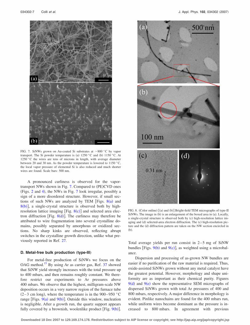
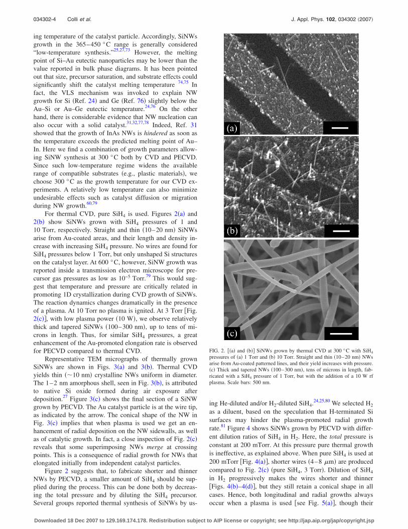
A pronounced curliness is observed for the vapor-transport NWs shown in Fig. 7. Compared to �PE�CVD ones�Figs. 2 and 4�, the NWs in Fig. 7 look irregular, possibly asign of a more disordered structure. However, if small sec-tions of such NWs are analyzed by TEM �Figs. 8�a� and8�b��, a single-crystal structure is observed both by high-resolution lattice imaging �Fig. 8�c�� and selected area elec-tron diffraction �Fig. 8�d��. The curliness may therefore beattributed to wire fragmentation into several crystalline do-mains, possibly separated by amorphous or oxidized sec-tions. No sharp kinks are observed, reflecting abruptswitches in the crystalline growth direction, unlike what pre-viously reported in Ref. 27.
D. Metal-free bulk production „type-III…
For metal-free production of SiNWs we focus on theOAG method.15 By using Ar as carrier gas, Ref. 37 showedthat SiNW yield strongly increases with the total pressure upto 400 mbars, and then remains roughly constant. We there-fore restrict our experiments to Ar pressures above400 mbars. We observe that the highest, milligram-scale NWdeposition occurs in a very narrow region of the furnace tube�2–3 cm long�, where the temperature is in the 900–950 °Crange �Figs. 9�a� and 9�b��. Outside this window, nucleationis negligible. After a growth run, the quartz support appearsfully covered by a brownish, woolenlike product �Fig. 9�b��.
Total average yields per run consist in 2–5 mg of SiNWbundles �Figs. 9�b� and 9�c��, as weighted using a microbal-ance.
Dispersion and processing of as-grown NW bundles areeasier if no purification of the raw material is required. Thus,oxide-assisted SiNWs grown without any metal catalyst havethe greatest potential. However, morphology and shape uni-formity are as important as their chemical purity. Figures9�d� and 9�e� show the representative SEM micrographs ofdispersed SiNWs grown with total Ar pressures of 400 and800 mbars, respectively. A major difference in morphology isevident. Pinlike nanochains are found for the 400 mbars run,while uniform wires become dominant as the pressure is in-creased to 800 mbars. In agreement with previous
FIG. 7. SiNWs grown on Au-coated Si substrates at �800 °C by vaportransport. The Si powder temperature is �a� 1250 °C and �b� 1150 °C. At1250 °C the wires are tens of microns in length, with average diameterbetween 20 and 30 nm. As the powder temperature is lowered to 1150 °C,the local vapor pressure of elemental Si is also reduced and much shorterwires are found. Scale bars: 500 nm.
FIG. 8. �Color online� ��a� and �b�� Bright-field TEM micrographs of type-IISiNWs. The image in �b� is an enlargement of the boxed area in �a�. Locally,a single-crystal structure is observed both by �c� high-resolution lattice im-aging and �d� selected-area electron diffraction. The �c� high-resolution pic-ture and the �d� diffraction pattern are taken on the NW section encircled in�b�.
034302-7 Colli et al. J. Appl. Phys. 102, 034302 �2007�
Downloaded 18 Dec 2007 to 129.169.174.178. Redistribution subject to AIP license or copyright; see http://jap.aip.org/jap/copyright.jsp

literature,37 the total yield remains roughly constant above400 mbars. We therefore conclude that the process pressureis a key parameter to promote a uniform NW morphology.
Pin-like structures or nanochains consist of crystalline Sispheres connected by SiO2 bridges of variable length andthickness.41,43,44 Figure 10�a� shows a bright-field TEM mi-crograph of a Si nanochain grown at 400 mbars. The corre-sponding energy-filtered TEM oxygen map shown in Fig.10�b� and the high-resolution transmission electron micros-copy �HRTEM� micrograph in Fig. 10�c� confirm previousobservations.41,43 The ball-to-ball separation in such
nanochains varies from 20 nm �as in Fig. 10�a�� to severalhundreds nanometers �see Fig. 9�c�� and is inhomogeneousand hardly reproducible at 400 mbars. Figure 10�d� shows abright-field TEM micrograph of SiNWs grown at 800 mbar.HR lattice imaging on such NWs �Fig. 10�e�� indicates a Sicrystalline core surrounded by an oxide shell, much thickerthan the native oxide thickness ��1–2 nm� observed forCVD SiNWs. A small fraction of nanochains or, more often,NWs with varying diameter is sometimes detected at800 mbars. In this case, however, the ball-to-ball distancedoes not exceed 2–3 nm. Oxide bridges of such a shortlength may behave as efficient tunneling barriers between thecrystalline Si nanospheres, and allow detection of singleelectron charging effects up to room temperature.44
Several aspects of the oxide-assisted growth model arestill debated.43,86–89 However, a possible explanation of thepressure-dependent shape control may be inferred. Reference43 proposed the formation of nanochains as consequence ofin situ partial oxidation of the as-synthesized NWs �possiblydue to residual oxygen�. Since the oxidation rate increaseswith temperature, this explains the observation that pinlikestructures are formed in a hotter region compared to NWs.43
Reference 86 also showed that oscillations in the Ar pressureduring growth lead to nanochains of controllable morphol-ogy. However, it did not explain if such a modulation effectoccurs synchronously with NW growth or happens post-nucleation.
In vapor transport, the material evaporating from theboat �furnace center, 1400 °C� is assumed to drift down-stream carried by the Ar flow and to condense on the tubewalls as soon as the temperature falls within the nucleationrange �900–950 °C�.15,37 In our case, however, a lower yieldof SiNWs is also found upstream the SiO boat, in the up-
FIG. 9. �Color online� �a� Scheme of the furnace deposition setup. �b� Bulkproduction of SiNWs. The quartz support is fully covered by brownish,woollen-like SiNW bundles. �c� SEM image of raw SiNWs bundles as col-lected from the quartz support. ��d� and �e�� SEM micrographs of oxide-assisted SiNWs grown at �d� 400 mbars, and �e� 800 mbars and dispersed onSi chips. Pinlike nanochain shapes are mainly found in �a�, while uniformwires become dominant as the pressure is increased to 800 mbars �b�. Scalebars: 1 �m.
FIG. 10. �a� Bright-field TEM micrograph of a Si nanochain, and �b� thecorresponding energy-filtered TEM oxygen map. �c� HRTEM of a single Sinanosphere confirming its crystalline nature. �d� Bright-field TEM micro-graph of oxide-assisted, uniform SiNWs. �e� HR lattice imaging of a NWpresented in �d�, showing a Si crystalline core surrounded by a 6-nm-thickamorphous shell.
034302-8 Colli et al. J. Appl. Phys. 102, 034302 �2007�
Downloaded 18 Dec 2007 to 129.169.174.178. Redistribution subject to AIP license or copyright; see http://jap.aip.org/jap/copyright.jsp

stream 900–950 °C region of the tube �see Fig. 9�a��. This isnot entirely surprising, since the vapor stream inside aseveral-centimeter-wide furnace tube is mainly due to diffu-sive transport, while the kinetic contribution due to the car-rier gas �at 50–100 SCCM� is less important or even negli-gible, as we have shown in Ref. 45. Hence, since vaportransport is diffusion driven, oxygen diffusion can also besuppressed if the total Ar pressure is increased. This couldexplain the negligible oxidation rate we reproducibly achieveat 800 mbars.
IV. NANOWIRE DISPERSION
Ongoing research suggests that polymer/CNT compos-ites may exhibit unique characteristics in terms ofmechanical90 and optical91,92 properties. Hence, we investi-gate the dispersion of SiNWs in various organic solvents�ethanol, isopropyl alcohol �IPA�, water, chloroform, toluene,dimethylformamide �DMF�, and xylene� with the aim offorming polymer/SiNW composites.
For dispersion studies we use type-III SiNWs, since theOAG method gives the highest yield. Achieving effectivedispersion of raw bundles is not immediate though, asSiNWs tend to form large aggregates. To achieve this, weuse ultrasonication. We find that typical ultrasonic baths arecapable of dispersing SiNWs, but an efficient debundlingrequires up to several hours. As an alternative, we obtaineffective and rapid dispersion by means of high power soni-cation �e.g., tip sonication�. This method, however, deliversmuch shorter wires because of fragmentation. We thus use acompromise process where SiNW bundles are inserted in acuvette containing the solvent, and then placed in a 200 W,20 kHz sonication bath �Bioruptor, Diagenode�. Here, sonicwaves emanate from the base of the water bath, and arereflected by a metal tip inserted in the cuvette.93 Sonic wavesare both concentrated and distributed within the cuvettewithout being localized, as in the case of a sonication tip,where the sonic waves are solely distributed from the base ofthe tip �see Fig. 11�a��.
There is no mechanical effect on the crystalline qualityof the wires due to sonication. High-resolution TEM andXRD do not indicate a significant increase of defects or dis-order in dispersed NWs. The main consequence of highpower sonication is to break long NWs into shorter frag-ments, though their single-crystal nature is maintained.
Our experiments indicate that IPA allows solution pro-cessing of SiNWs without the need of a surfactant. Follow-ing sonication, our IPA suspensions �up to 0.1 g/ l� are stablefor several days and are a consistent light yellow, Fig. 11�b�.We did not achieve dispersion in toluene, xylene, and chlo-roform, where precipitation of SiNWs is observed, Fig.11�c�. It is well known that the solubility of solution-grownnanocrystals depends on a proper combination betweenpolar/nonpolar solvents and hydrophobic/hydrophilicsurfaces.94 Similarly, the hydrophilic SiO2 shell surroundingthe wires triggers an easy dispersion of SiNWs in polar sol-vents and causes precipitation in nonpolar ones.
Dispersing semiconducting polymers and SiNWs in thesame solvent facilitates the formation of mixtures. Contrary
to what is seen above for SiNWs, however, semiconductingorganic molecules �e.g., poly-3-hexylthiophene �P3HT�,poly�9,9-dioctylfluorene-co-bithiophene� �F8T2�, poly�3,3-dialkyl-quaterthiophene� �PQT�� tend to be far more easilydissolved in nonpolar solvents, such as xylene. Attempts topromote dispersion of SiNWs in xylene using surfactantssuch as octadecylamine �which was used in Ref. 46 in com-bination with isooctane and IPA� did not improve the results.Still, we found that N-methyl-2-pyrrolidone �NMP�, a dipo-lar aprotic solvent, behaves as a good compromise solvent inwhich stable solutions of both SiNWs �with concentrationssimilar to that of IPA solutions� and organic semiconductors�PQT, for instance� can be formed. This provides a promisingapproach to achieve high-concentration NW/polymer com-posites. As a further step, we demonstrated the feasibility ofink-jet printing of nanostructured materials �such as SiNWs,Figs. 11�d� and 11�e�� for a variety of applications,95 whichopens opportunities for inexpensive large area fabrication ofplastic electronics.
V. ELECTRICAL TRANSPORT
Figure 12 compares representative transfer curves�IDS-VGS� for SiNWs grown by the different methods de-scribed in Sec. III. The devices are interdigitated multiple-
FIG. 11. �Color online� �a� Scheme of the sonicator operation principle.Samples are contained in a cuvette that is placed in a water bath. Here, sonicwaves emanate from the base of the water bath, and are reflected by a tipinserted in the cuvette containing the solution of SiNWs.93 �b� stable SiNWdispersion in IPA or NMP. �c� SiNW precipitation when xylene is used assolvent. �d� SEM micrograph of ink-jetted SiNWs using the solution shownin �b�. Scale bar: 1 �m. �e� 500-�m-wide drops of PQT-SiNW compositeafter ink jetting onto predefined contact arrays. Scale bar: 500 �m.
034302-9 Colli et al. J. Appl. Phys. 102, 034302 �2007�
Downloaded 18 Dec 2007 to 129.169.174.178. Redistribution subject to AIP license or copyright; see http://jap.aip.org/jap/copyright.jsp

channel planar FETs, as illustrated in Fig. 12�a�. Comparedto single-NW FETs, our devices are more representative of agiven growth technique, since a large statistics integratedover several NWs is considered. A qualitative analysis ofFig. 12�b� shows that all our SiNW FETs switch on for nega-tive gate voltages, which is an indication of hole-dominatedtransport. The normalized transconductance can be extractedfrom the slope dIDS/dVGS in the left part of the curve dividedby the effective channel width Nd, where d is the averagewire diameter and N is the number of wires contacted withinthe same device.8 Curves in Fig. 12�b� correspond to deviceswith 7, 24, and 10 SiNWs �for types I, II, and III, respec-tively�. These give very similar values �28–40 nS �m−1� forthe normalized transconductance, which turns out to be sen-sibly lower than other reports available in the literature.8 We
also observe that type-II SiNWs show ambipolar behavior,i.e., electron injection occurs for positive gate voltages. Thecurrent due to electrons, however, always shows a lower sub-threshold slope compared to holes �see also Fig. 12�c�, wheretransfer curves are plotted on a log scale�. The ambipolareffect is reproducibly observed for type-II SiNWs, while itnever occurs for type I or type III. We note from Figs. 12�b�and 12�c� that our ambipolar devices cannot be completelyturned off, but a residual current is detected at room tempera-ture for intermediate gate voltages.
Figure 13 plots the corresponding output curves�IDS-VSD� for all types of SiNWs, measured for gate voltagescorresponding to the on states. For ambipolar SiNWs, wealso show the output curve for the on state due to electronpopulation �i.e., for high positive gate voltages�. In all cases,a clear nonlinearity is observed in the output curves, indicat-ing that the contacts between NWs and metal leads are notOhmic but rather a Schottky barrier is present.96 Typical totaldevice resistances in the on state are in the 1–100 M�range. We note, however, that the output curves are oftennon-symmetric when reversing the applied bias. This effectis amplified if the number of NWs within a single device isreduced. We conclude that contacts are in general non-equivalent and a wide distribution of contact resistances mayexist for a single fabrication process, leading to a situationwhere only a few wires are dominating the electrical trans-port for an individual device. This can mislead the estimationof normalized FET parameters.
A direct comparison of the absolute threshold voltagesmeasured for different devices is quite challenging becauseof hysteresis effects. Hysteresis in IDS-VGS measurements forCNT- or NW-based FETs has been widely reported, andmainly attributed to charge trapping in the surface states ofSiO2.8,41,61,97 Such charges may generate electric fields ofopposite sign superimposed to the applied gate voltage. Asan example, in Fig. 14 we show IDS-VGS curves for type-INWs for different gate sweeping ranges. If two curves areconsecutively collected by sweeping the gate voltage from−10 to 10 V and vice versa �solid lines�, only a small hys-
FIG. 12. �Color online� �a� Scheme and SEM micrograph of interdigitatedmultiple-channel planar SiNW FETs. Scalebar: 1 �m. �b� Representativetransfer curves �IDS-VGS� for SiNWs grown by different methods. Curvescorrespond to devices with 7, 24, and 10 SiNWs �for types I, II, and III,respectively�. �c� Transfer curves for SiNWs plotted on a vertical log scale,showing the maximum/minimum on/off currents.
FIG. 13. �Color online� Output curves �IDS-VSD�, corresponding to devicespresented in Fig. 12, measured for gate voltages corresponding to the onstates. For ambipolar SiNWs, we also show the output curve for the on statedue to electron population.
034302-10 Colli et al. J. Appl. Phys. 102, 034302 �2007�
Downloaded 18 Dec 2007 to 129.169.174.178. Redistribution subject to AIP license or copyright; see http://jap.aip.org/jap/copyright.jsp
teresis is seen. However, if the sweeping range is extendedfrom −30 to 30 V, a big shift, up to 35 V, is observed whenreversing the scan �dotted lines�. This shows that the trappedcharge screening is proportional to the initial gate field ap-plied. Such memory effect is stable for several hours in airand at room temperature, and no quick discharge is possibleto reproduce the original measurement conditions.
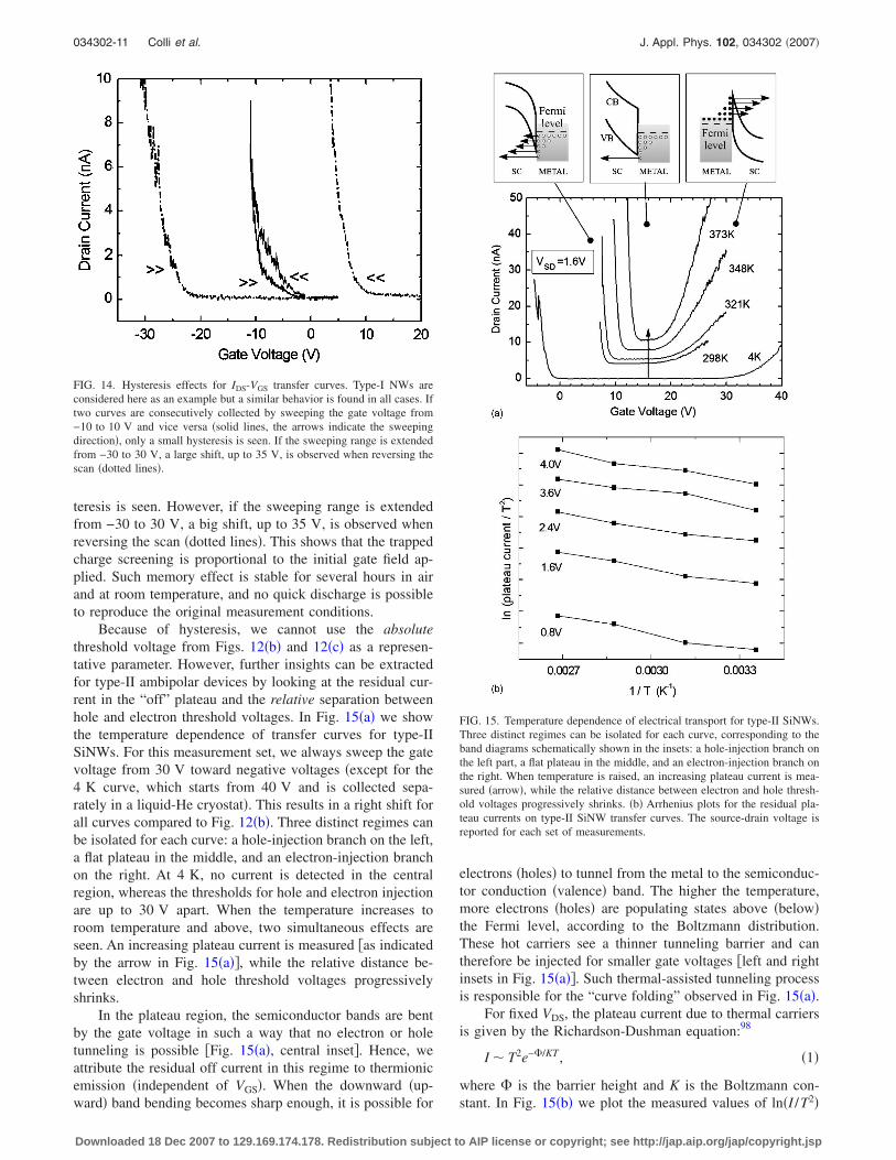
Because of hysteresis, we cannot use the absolutethreshold voltage from Figs. 12�b� and 12�c� as a represen-tative parameter. However, further insights can be extractedfor type-II ambipolar devices by looking at the residual cur-rent in the “off” plateau and the relative separation betweenhole and electron threshold voltages. In Fig. 15�a� we showthe temperature dependence of transfer curves for type-IISiNWs. For this measurement set, we always sweep the gatevoltage from 30 V toward negative voltages �except for the4 K curve, which starts from 40 V and is collected sepa-rately in a liquid-He cryostat�. This results in a right shift forall curves compared to Fig. 12�b�. Three distinct regimes canbe isolated for each curve: a hole-injection branch on the left,a flat plateau in the middle, and an electron-injection branchon the right. At 4 K, no current is detected in the centralregion, whereas the thresholds for hole and electron injectionare up to 30 V apart. When the temperature increases toroom temperature and above, two simultaneous effects areseen. An increasing plateau current is measured �as indicatedby the arrow in Fig. 15�a��, while the relative distance be-tween electron and hole threshold voltages progressivelyshrinks.
In the plateau region, the semiconductor bands are bentby the gate voltage in such a way that no electron or holetunneling is possible �Fig. 15�a�, central inset�. Hence, weattribute the residual off current in this regime to thermionicemission �independent of VGS�. When the downward �up-ward� band bending becomes sharp enough, it is possible for
electrons �holes� to tunnel from the metal to the semiconduc-tor conduction �valence� band. The higher the temperature,more electrons �holes� are populating states above �below�the Fermi level, according to the Boltzmann distribution.These hot carriers see a thinner tunneling barrier and cantherefore be injected for smaller gate voltages �left and rightinsets in Fig. 15�a��. Such thermal-assisted tunneling processis responsible for the “curve folding” observed in Fig. 15�a�.
For fixed VDS, the plateau current due to thermal carriersis given by the Richardson-Dushman equation:98
I � T2e−�/KT, �1�
where � is the barrier height and K is the Boltzmann con-stant. In Fig. 15�b� we plot the measured values of ln�I /T2�
FIG. 14. Hysteresis effects for IDS-VGS transfer curves. Type-I NWs areconsidered here as an example but a similar behavior is found in all cases. Iftwo curves are consecutively collected by sweeping the gate voltage from−10 to 10 V and vice versa �solid lines, the arrows indicate the sweepingdirection�, only a small hysteresis is seen. If the sweeping range is extendedfrom −30 to 30 V, a large shift, up to 35 V, is observed when reversing thescan �dotted lines�.
FIG. 15. Temperature dependence of electrical transport for type-II SiNWs.Three distinct regimes can be isolated for each curve, corresponding to theband diagrams schematically shown in the insets: a hole-injection branch onthe left part, a flat plateau in the middle, and an electron-injection branch onthe right. When temperature is raised, an increasing plateau current is mea-sured �arrow�, while the relative distance between electron and hole thresh-old voltages progressively shrinks. �b� Arrhenius plots for the residual pla-teau currents on type-II SiNW transfer curves. The source-drain voltage isreported for each set of measurements.
034302-11 Colli et al. J. Appl. Phys. 102, 034302 �2007�
Downloaded 18 Dec 2007 to 129.169.174.178. Redistribution subject to AIP license or copyright; see http://jap.aip.org/jap/copyright.jsp

as a function of 1/T, in order to estimate the barrier height.This temperature dependence was measured for several VDS
�0.8–4 V�, and a very similar slope was extracted in allcases. By combining the whole data set, we obtain a maxi-mum activation energy of 0.08 eV �0.06±0.02�. Since holeinjection appears most favorable and leads to lower deviceresistances �see Figs. 12 and 13�, this value reflects theSiNW valence band offset with respect to the Fermi level ofthe metal.
It has been pointed out that, for nominally undopedSiNWs, the valence band is pinned to the Fermi level of themetal contacts, resulting in p-type semiconductingbehavior.57,61,96 This is not surprising, since interfacial statesin many metal-semiconductor junctions tend to generate anoffset between valence band and Fermi level which isroughly 1/3 of the semiconductor band gap.99,100 Yet, mea-sured � is lower than that reported in previous experimentsand theoretical predictions.57,96,99–101 Further investigationson the nanoscopic nature of the metal-NW contacts areneeded in order to clarify this discrepancy.
For type-III SiNWs, Ref. 41 attributed the observedp-type behavior to B incorporation during growth. For thesame type of wires, however, we measure a similar curvedespite the absence of dopants �Fig. 12�b��. For type-ISiNWs, Ref. 57 reported a nominally intrinsic NW devicewith almost ideal Al Ohmic contacts, though inferring thepresence of a small Schottky barrier compared to heavilydoped NWs. It is generally hard to quantify precisely lowdoping concentrations in SiNWs and the resulting bandalignment, unless ambipolar devices are considered �see Ref.62 for an extensive comparison�.
Our study aims to identify general differences in theelectrical response due to different growth protocols. There-fore, our devices are not annealed after contact fabrication�unlike most previous works3,56,60–62�. This minimizes effectssuch as catalyst diffusion,60 which could alter the comparisonbetween wires grown by different processes. Type-II wirescould have some contamination �possibly due to backgrounddoping� due to low-vacuum synthesis environment combinedwith the possible diffusion of the Au catalyst at the highgrowth temperatures used ��800 °C�.60 Since ambipolar be-havior of NWs is generally regarded as a fingerprint of in-trinsic material,18,102 we deduce that no detrimental effect isintroduced by the type-II growth procedure compared totypes I and III. Indeed, it remains an open question whyambipolar behavior is not seen for type-I or type-III NWs.Despite this discrepancy, however, in all cases device perfor-mance seems mainly dominated by the metal contacts, irre-spective of how the NW active channels are fabricated orassembled.
VI. CONCLUSION
We investigated and compared multiple routes to SiNWsynthesis. As a function of the selected deposition technique,we achieved different yields, selective Au-catalyzed growth,bulk catalyst-free production, different nanocrystal mor-phologies, and relatively high or low nucleation tempera-tures. For each synthesis protocol, we highlighted the experi-
mental parameters leading to morphology control.Concentrated and stable dispersions of SiNWs were obtainedin solvents compatible with semiconducting organic poly-mers. Similar electrical properties are measured for SiNWsgrown by different methods. All the considered FETs fabri-cated from intrinsic SiNWs show a preferential p-type be-havior with comparable performance. In addition, devicesbased on Au-assisted SiNWs grown by thermal evaporationof Si powders �type II� are ambipolar. This indicates that nodetrimental effects are introduced by using a metal catalyst,nor a low-vacuum furnace tube as deposition reactor.
ACKNOWLEDGMENTS
We thank L. Businaro, F. Romanato, and M. Lazzarinofor support in e-beam and x-Ray lithography at LILIT beam-line �Elettra-Trieste�. We also thank R. E. Dunin-Borkowskifor assistance in EFTEM mapping, P. Migliorato, M. Shaffer,and Z. A. K. Durrani for useful discussions. We acknowledgefunding from the EU project CANAPE, Advance Nanotech,Peterhouse, Pembroke College, EPSRC, The Royal Society,The Leverhulme Trust, and the Ministry of Information andCommunication, Republic of Korea �Project No. A1100-0602-0101�.
1Y.-J. Doh, J. A. van Dam, A. L. Roest, E. P. A. M. Bakkers, L. P. Kou-wenhoven, and S. De Franceschi, Science 309, 272 �2005�.
2S. Jin, D. Whang, M. C. McAlpine, R. S. Friedman, Y. Wu, and C. M.Lieber, Nano Lett. 4, 915 �2004�.
3M. C. McAlpine, R. S. Friedman, S. Jin, K. H. Lin, W. U. Wang, and C.M. Lieber, Nano Lett. 3, 1531 �2003�.
4Y. Huang, X. Duan, and C. M. Lieber, Small 1, 142 �2005�.5C. Thelander, H. A. Nilsson, L. E. Jensen, and L. Samuelson, Nano Lett.5, 635 �2005�.
6I. Gur, N. A. Fromer, M. L. Geier, and A. P. Alivisatos, Science 310, 462�2005�.
7M. Law, L. E. Greene, J. C. Johnson, R. Saykally, and P. Yang, Nat. Mater.4, 455 �2005�.
8X. Duan, C. Niu, V. Sahi, J. Chen, J. W. Parce, S. Empedocles, and J. L.Goldman, Nature �London� 425, 274 �2003�.
9Y. Huang, X. Duan, Y. Cui, L. J. Lauhon, K.-H. Kim, and C. M. Lieber,Science 294, 1313 �2001�.
10Z. Zhong, D. Wang, Y. Cui, M. W. Bockrath, and C. M. Lieber, Science302, 1377 �2003�.
11S. Piscanec, M. Cantoro, A. C. Ferrari, A. Zapien, Y. Lifshitz, S. T. Lee, S.Hofmann, and J. Robertson, Phys. Rev. B 68, 241312�R� �2003�.
12H. Scheel, S. Reich, A. C. Ferrari, M. Cantoro, A. Colli, and C. Thomsen,Appl. Phys. Lett. 88, 233114 �2006�.
13C. B. Murray, C. R. Kagan, and M. G. Bawendi, Annu. Rev. Mater. Sci.30, 545 �2000�.
14Y. Yin and A. P. Alivisatos, Nature �London� 437, 664 �2005�.15R. Q. Zhang, Y. Lifshitz, and S. T. Lee, Adv. Mater. �Weinheim, Ger.� 15,
635 �2003�.16A. M. Morales and C. M. Lieber, Science 279, 208 �1998�.17T. Mårtensson, P. Carlberg, M. Borgstrom, L. Montelius, W. Seifert, and
L. Samuelson, Nano Lett. 4, 699 �2004�.18J. Goldberger, A. I. Hochbaum, R. Fan, and P. Yang, Nano Lett. 6, 973
�2006�.19Y. F. Zhang, Y. H. Tang, N. Wang, D. P. Yu, C. S. Lee, I. Bello, and S. T.
Lee, Appl. Phys. Lett. 72, 1835 �1998�.20D. P. Yu et al., Appl. Phys. Lett. 72, 3458 �1998�.21F. M. Kolb, H. Hofmeister, R. Scholz, M. Zacharias, U. Gosele, D. D. Ma,
and S. T. Lee, J. Electrochem. Soc. 151, G472 �2004�.22J. Hu, Y. Bando, J. Zhan, Z. Liu, D. Golberg, and S. P. Ringer, Adv. Mater.
�Weinheim, Ger.� 17, 975 �2005�.23N. D. Zakharov, P. Werner, G. Gerth, L. Schubert, L. Sokolov, and U.
Gosele, J. Cryst. Growth 290, 6 �2006�.24J. Westwater, D. P. Gosain, S. Tomiya, S. Usui, and H. Ruda, J. Vac. Sci.
Technol. B 15, 554 �1997�.
034302-12 Colli et al. J. Appl. Phys. 102, 034302 �2007�
Downloaded 18 Dec 2007 to 129.169.174.178. Redistribution subject to AIP license or copyright; see http://jap.aip.org/jap/copyright.jsp

25Yi Cui, L. J. Lauhon, M. S. Gudiksen, J. Wang, and C. M. Lieber, Appl.Phys. Lett. 78, 2214 �2001�.
26A. I. Hochbaum, R. Fan, R. He, and P. Yang, Nano Lett. 5, 457 �2005�.27S. Hofmann, C. Ducati, R. J. Neill, S. Piscanec, A. C. Ferrari, J. Geng, R.
E. Dunin-Borkowski, and J. Robertson, J. Appl. Phys. 94, 6005 �2003�.28R. S. Wagner and W. C. Ellis, Appl. Phys. Lett. 4, 89 �1964�.29E. I. Givargizov, J. Cryst. Growth 31, 20 �1975�.30A. I. Persson, M. W. Larsson, S. Stenström, B. J. Ohlsson, L. Samuelson,
and L. R. Wallenberg, Nat. Mater. 3, 677 �2004�.31K. A. Dick, K. Deppert, T. Martensson, B. Mandl, L. Samuelson, and W.
Seifert, Nano Lett. 5, 761 �2005�.32A. Colli et al., Appl. Phys. Lett. 86, 153103 �2005�.33A. Colli, S. Hofmann, A. C. Ferrari, F. Martelli, S. Rubini, C. Ducati, A.
Franciosi, and J. Robertson, Nanotechnology 16, S139 �2005�.34S. Hofmann, G. Csányi, A. C. Ferrari, M. C. Payne, and J. Robertson,
Phys. Rev. Lett. 95, 036101 �2005�.35J. Liu et al., Science 280, 1253 �1998�.36A. Colli et al., AIP Conf. Proc. 723, 445 �2004�.37Y. F. Zhang, Y. H. Tang, C. Lam, N. Wang, C. S. Lee, I. Bello, and S. T.
Lee, J. Cryst. Growth 212, 115 �2000�.38N. Wang, Y. F. Zhang, Y. H. Tang, C. S. Lee, and S. T. Lee, Appl. Phys.
Lett. 73, 3902 �1998�.39B. Mandl, J. Stangl, T. Martensson, A. Mikkelsen, J. Eriksson, L. S. Karls-
son, G. Bauer, L. Samuelson, and W. Seifert, Nano Lett. 6, 1817 �2006�.40H. D. Park, S. M. Prokes, M. E. Twigg, R. C. Cammarata, and A. C.
Gaillot, Appl. Phys. Lett. 89, 223125 �2006�.41K. Byon, D. Tham, J. E. Fischer, and A. T. Johnson, Appl. Phys. Lett. 87,
193104 �2005�.42Z. W. Pan, Z. R. Dai, L. Xu, S. T. Lee, and Z. L. Wang, J. Phys. Chem. B
105, 2507 �2001�.43H. Y. Peng, Z. W. Pan, L. Xu, X. H. Fan, N. Wang, C. S. Lee, and S. T.
Lee, Adv. Mater. �Weinheim, Ger.� 13, 317 �2001�.44M. A. Rafiq, A. Colli, P. Servati, Z. A. K. Durrani, A. C. Ferrari, W. I.
Milne, and H. Mizuta �unpublished�.45A. Colli, A. Fasoli, S. Hofmann, C. Ducati, J. Robertson, and A. C. Fer-
rari, Nanotechnology 17, 1046 �2006�.46Z. R. Dai, Z. W. Pan, and Z. L. Wang, Adv. Funct. Mater. 13, 9 �2003�.47D. Whang, S. Jin, Y. Wu, and C. M. Lieber, Nano Lett. 3, 1255 �2003�.48J. Z. He et al., Appl. Phys. Lett. 80, 1812 �2002�.49L. Dong, J. Bush, V. Chirayos, R. Solanki, J. Jiao, Y. Ono, J. F. Conley,
and B. D. Ulrich, Nano Lett. 5, 2112 �2005�.50S. M. King, S. Chaure, J. Doyle, A. Colli, A. C. Ferrari, and W. J. Blau,
Opt. Commun. 276, 305 �2007�.51M. J. O’Connell et al., Science 297, 593 �2002�.52S. Giordani, S. D. Bergin, V. Nicolosi, S. Lebedkin, M. M. Kappes, W. J.
Blau, and J. N. Coleman, J. Phys. Chem. B 110, 15708 �2006�.53M. J. O’Connell et al., Chem. Phys. Lett. 342, 265 �2001�.54H. J. Snaith, G. L. Whiting, B. Sun, N. C. Greenham, W. T. S. Huck, and
R. H. Friend, Nano Lett. 5, 1653 �2005�.55I. Gur, N. A. Fromer, C. P. Chen, A. G. Kanaras, and A. P. Alivisatos,
Nano Lett. 7, 409 �2007�.56Y. Cui, Z. Zhong, D. Wang, W. U. Wang, and C. M. Lieber, Nano Lett. 3,
149 �2003�.57Y. Cui, X. Duan, J. Hu, and C. M. Lieber, J. Phys. Chem. B 104, 5213
�2000�.58Y. H. Tang, X. H. Sun, F. C. K. Au, L. S. Liao, H. Y. Peng, C. S. Lee, S.
T. Lee, and T. K. Sham, Appl. Phys. Lett. 79, 1673 �2001�.59G. Zheng, W. Lu, S. Jin, and C. M. Lieber, Adv. Mater. �Weinheim, Ger.�
16, 1890 �2004�.60J. Y. Yu, S. W. Chung, and J. R. Heath, J. Phys. Chem. B 104, 11864
�2000�.61Y. Ahn, J. Dunning, and J. Park, Nano Lett. 5, 1367 �2005�.62W. M. Weber et al., Nano Lett. 6, 2660 �2006�.63D. N. Jarrett and L. Ward, J. Phys. D 9, 1515 �1976�.
64E. Jiran and C. V. Thompson, J. Electron. Mater. 19, 1153 �1990�.65R. H. Doremus, J. Appl. Phys. 37, 2775 �1966�.66U. Kreibig and L. Genzel, Surf. Sci. 156, 678 �1985�.67L. Zhao, K. L. Kelly, and G. C. Schatz, J. Phys. Chem. B 107, 7343
�2003�.68M. Cantoro et al., Nano Lett. 6, 1107 �2006�; M. Cantoro, S. Hofmann, S.
Pisana, C. Ducati, A. Parvez, A. C. Ferrari, and J. Robertson, DiamondRelat. Mater. 15, 1029 �2006�.
69A. L. Giermann and C. V. Thompson, Appl. Phys. Lett. 86, 121903�2005�.
70S. Hofmann, M. Cantoro, B. Kleinsorge, C. Casiraghi, A. Parvez, J. Rob-ertson, and C. Ducati, J. Appl. Phys. 98, 034308 �2005�.
71S. Pisana, M. Cantoro, A. Parvez, S. Hofmann, A. C. Ferrari, and J. Rob-ertson, Physica E �Amsterdam� 37, 1 �2007�.
72T. B. Massalski, Binary Alloy Phase Diagrams, 2nd ed. �ASM Interna-tional, Materials Park, OH, 1990�.
73J. Kikkawa, Y. Ohno, and S. Takeda, Appl. Phys. Lett. 86, 123109 �2005�.74P. Buffat and J. P. Borel, Phys. Rev. A 13, 2287 �1976�.75A. Jiang, N. Awasthi, A. N. Kolmogorov, W. Setyawan, A. Borjesson, K.
Bolton, A. R. Harutyunyan, and S. Curtarolo, Phys. Rev. B 75, 205426�2007�.
76A. B. Greytak, L. J. Lauhon, M. S. Gudiksen, and C. M. Lieber, Appl.Phys. Lett. 84, 4176 �2004�.
77T. I. Kamins, R. S. Williams, D. P. Basile, T. Hesjedal, and J. S. Harris, J.Appl. Phys. 89, 1008 �2001�.
78Y. Wang, V. Schmidt, S. Senz, and U. Gosele, Nat. Nanotechnol. 1, 186�2006�.
79J. B. Hannon, S. Kodambaka, F. M. Ross, and R. M. Tromp, Nature�London� 440, 69 �2006�.
80Y. Wu, Y. Cui, L. Huynh, C. J. Barrelet, D. C. Bell, and C. M. Lieber,Nano Lett. 4, 433 �2004�.
81L. J. Lauhon, M. S. Gudiksen, and C. M. Lieber, Philos. Trans. R. Soc.London, Ser. A 362, 1247 �2004�.
82L. Cao, L. Laim, C. Ni, B. Nabet, and J. E. Spanier, J. Am. Chem. Soc.127, 13782 �2005�.
83C. B. Jin, J. E. Yang, and M. H. Jo, Appl. Phys. Lett. 88, 193105 �2006�.84R. Weast, Handbook of Chemistry and Physics, 64th ed. �Chemical Rub-
ber, Cleveland, 1983�.85S. Kodambaka, J. B. Hannon, R. M. Tromp, and F. M. Ross, Nano Lett. 6,
1292 �2006�.86X. H. Sun, N. B. Wong, C. P. Li, S. T. Lee, and T. K. Sham, J. Appl. Phys.
96, 3447 �2004�.87Y. F. Zhang, Y. H. Tang, N. Wang, C. S. Lee, I. Bello, and S. T. Lee, J.
Cryst. Growth 197, 136 �1999�.88R. J. Barsotti, Jr., J. E. Fischer, C. H. Lee, J. Mahmood, C. K. W. Adu, and
P. Eklund, Appl. Phys. Lett. 81, 2866 �2002�.89J. Hu, Y. Bando, J. Zhan, Z. Liu, D. Goldberg, and S. P. Ringer, Adv.
Mater. �Weinheim, Ger.� 17, 975 �2005�.90A. B. Dalton et al., Nature �London� 423, 703 �2003�.91V. Scardaci, A. G. Rozhin, F. Hennrich, W. I. Milne, and A. C. Ferrari,
Physica E �Amsterdam� 37, 115 �2007�.92G. Della Valle et al., Appl. Phys. Lett. 89, 231115 �2006�.93http://www.diagenode.com/pages/bioruptor.html94T. Pellegrino et al., Nano Lett. 4, 703 �2004�.95P. Beecher et al., J. Appl. Phys. �in press�.96S. W. Chung, J. Y. Yu, and J. R. Heath, Appl. Phys. Lett. 76, 2068 �2000�.97D. Wang, Y. L. Chang, Q. Wang, J. Cao, D. B. Farmer, R. G. Gordon, and
H. Dai, J. Am. Chem. Soc. 126, 11602 �2004�.98S. M. Sze, Physics of Semiconductor Devices �Wiley, New York, 1981�.99A. M. Cowley and S. M. Sze, J. Appl. Phys. 36, 3212 �1965�.100C. A. Mead and W. G. Spitzer, Phys. Rev. 134, A713 �1964�.101M. O. Aboelfotoh and K. N. Tu, Phys. Rev. B 34, 2311 �1986�.102S. M. Koo, M. D. Edelstein, Q. Li, C. A. Richter, and E. M. Vogel,
Nanotechnology 16, 1482 �2005�.
034302-13 Colli et al. J. Appl. Phys. 102, 034302 �2007�
Downloaded 18 Dec 2007 to 129.169.174.178. Redistribution subject to AIP license or copyright; see http://jap.aip.org/jap/copyright.jsp