Theoretical Analysis & Practical Implementation of a Super ...
66
Lehigh University Lehigh Preserve eses and Dissertations 2017 eoretical Analysis & Practical Implementation of a Super-Regenerative Receiver for Amplitude Modulated Radio Signals Anthony Michael Evelina Lehigh University Follow this and additional works at: hps://preserve.lehigh.edu/etd Part of the Electrical and Electronics Commons is esis is brought to you for free and open access by Lehigh Preserve. It has been accepted for inclusion in eses and Dissertations by an authorized administrator of Lehigh Preserve. For more information, please contact [email protected]. Recommended Citation Evelina, Anthony Michael, "eoretical Analysis & Practical Implementation of a Super-Regenerative Receiver for Amplitude Modulated Radio Signals" (2017). eses and Dissertations. 4229. hps://preserve.lehigh.edu/etd/4229
Transcript of Theoretical Analysis & Practical Implementation of a Super ...

Lehigh UniversityLehigh Preserve
Theses and Dissertations
2017
Theoretical Analysis & Practical Implementation ofa Super-Regenerative Receiver for AmplitudeModulated Radio SignalsAnthony Michael EvelinaLehigh University
Follow this and additional works at: https://preserve.lehigh.edu/etd
Part of the Electrical and Electronics Commons
This Thesis is brought to you for free and open access by Lehigh Preserve. It has been accepted for inclusion in Theses and Dissertations by anauthorized administrator of Lehigh Preserve. For more information, please contact [email protected].
Recommended CitationEvelina, Anthony Michael, "Theoretical Analysis & Practical Implementation of a Super-Regenerative Receiver for AmplitudeModulated Radio Signals" (2017). Theses and Dissertations. 4229.https://preserve.lehigh.edu/etd/4229

Theoretical Analysis & Practical Implementation of a
Super-Regenerative Receiver for Amplitude Modulated
Radio Signals
By
Anthony M. Evelina Jr.
A Thesis
Presented to the Graduate and Research Committee
Of Lehigh University
In Candidacy for the Degree of
Master of Science
in
Electrical Engineering
Lehigh University
December 2017

ii
© Copyright by Anthony Evelina 2017
All Rights Reserved

iii
Thesis is accepted and approved in partial fulfillment of the requirements for the Master
of Science in Electrical Engineering.
Theoretical Analysis & Practical Implementation of a Super-Regenerative Receiver for
Amplitude Modulated Radio Signals
Anthony M. Evelina Jr.
Date Approved
Douglas R. Frey (Advisor)
Chengshan Xiao (Department Chair)

iv
Acknowledgements
First and foremost, I would like to express my deep respect and gratitude to my
parents for their unconditional love and support throughout my academic career. I am
forever grateful for the opportunities they have granted me, and I would like to dedicate
my accomplishments with this project to them.
Furthermore, I would like to express my sincere gratitude to my thesis and
graduate advisor, Professor Douglas Frey. His influence and teachings throughout my
undergraduate studies at Lehigh fully inspired me to pursue a higher education and work
towards a Master’s of Science in Electrical Engineering. He has consistently challenged
me to improve myself as an engineer both in and out of the classroom, which encouraged
me to take on this project in the first place. I attribute my successes here at Lehigh and
my continuously growing passion for engineering to him and I am truly appreciative of
his guidance throughout my time spent here.

v
Table of Contents
Acknowledgements .................................................................................................. iv
List of Tables & Figures ………………………………………………………… v
Abstract …………………………………………………………………………… 1
Chapter 1 Introduction ………………………………………………………… 2
1.1 Brief History of the Super-Regenerative Receiver ……………… 2
1.2 Principle of Regeneration………………………………………… 3
Chapter 2 Super-Regenertive Operation & Review of Relevant Concepts … 4
2.1 SRR Input Stage & Review of Amplitude Modulation ……… 4
2.2 Super-Regenerative Oscillator & Review of Feedback ……… 6
2.3 Detecting the SRO Output & Review of Demodulation ………… 10
Chapter 3 Mathematical Analysis of the Classical SRR ……………………… 12
3.1 Characteristic Equation of SRR ……………………………… 12
3.2 Damping Function ……………………………………………… 13
3.3 Sensitivity ……………………………………………………… 16
3.4 Solution of the Differential Equation ……………………… 17
3.4.1 Homogenous Solution: Free Response ……… 17
3.4.2 Particular Solution: Forced Response ……… 19
3.5 Redefining Gain & Compact Expression of Complete Solution 20
3.5.1 SRR Response to an RF Pulse When Tuned to Carrier
Frequency ……………………………………………… 22
3.5.2 SRR Response to an RF Pulse of Arbitrary Carrier
Frequency ……………………………………………… 24

vi
3.5.3 Response to a Sinusoidal Input ……………… 25
3.6 Hangover ……………………………………………………… 26
Chapter 4 Simulation of the Classical SRR ……………………………… 29
4.1 Simulation Model ……………………………………………… 29
4.2 Simulation of Ideal SRR Operation……………………………… 30
4.3 Multiple Resonance Due to Increasing Quench Frequency……… 32
4.4 Hangover Due to a Reducing the Quiescent Damping Factor…… 33
4.5 Simulation With an Amplitude Modulated Input Signal ……… 34
Chapter 5 Electrical Model & Practical Implementation ……………… 38
5.1 Electrical Model ……………………………………………… 38
5.2 Self-Quenching ……………………………………………… 41
5.3 Colpitts Oscillator ……………………………………………… 41
5.4 Alternative Time-Varying Gain Element ……………………… 43
5.5 Proposed Design & Simulation ……………………………… 48
Chapter 6 Conclusions & Future Work ……………………………………… 54
References ……………………………………………………………………… 56
Biography ……………………………………………………………………… 58

vii
List of Tables & Figures
Figure 1-1. Block diagram of the classical Super-Regenerative Receiver ……… 3
Figure 2-1a. Message signal (left), Carrier signal (right), and compound
waveform after multiplication (bottom) ……………………… 6
Figure 2-1b. Frequency representation of compound waveform in 2-1a ……… 6
Figure 2-2. (a) Impulse response and (b) frequency response of band pass filter 7
Figure 2-3a. Simple envelope detector for AM signals ……………………… 10
Figure 2-3b. Magnified view of envelope detector output ……………………… 10
Figure 3-1. Effect of a varying damping ratio on pole-zero plot of SRO ……… 14
Figure 3-2. (a) Sinusoidal damping function, (b) sensitivity and output curves,
(c) applied RF input pulse envelope ……………………………… 15
Figure 3-3. Frequency response of a high-Q (Red) and low-Q (Blue) system 18
Figure 3-4. SRR output pulse envelope for different hangover percentages 27
Figure 3-5. Effect of hangover on frequency response for different hangover
percentages (sinusoidal steady state) ……………………………… 27
Figure 4-1. Simulink model of SRR ……………………………………… 29
Table 4-1. Parameters for ideal SRR simulation ……………………………… 31
Figure 4-2. (a) RF input (b) SRO output (c) envelope detector ……………… 31
Figure 4-3. Simulation results given: 𝐾𝑜 = 1.5, 𝐾𝑎 = 1 (left) and
𝐾𝑎 = 1.5, 𝐾𝑜 = 1 (right) ……………………………………… 32
Figure 4-4. Frequency response due to change in quench frequency: (a) 𝑓𝑞 =
40 𝐾𝐻𝑧 (top left), (b) 𝑓𝑞 = 80 𝐾𝐻𝑧 (top right), (c) 𝑓𝑞 = 160 𝐾𝐻𝑧
(bottom left), (d) 𝑓𝑞 = 320 𝐾𝐻𝑧 (bottom right) ……………… 33

viii
Figure 4-5. SRR response to an input RF pulse given a high (left) and low (right)
quiescent damping factor ……………………………………… 34
Figure 4-6. Modified SRR Model ……………………………………………… 35
Figure 4-7. SRR simulation with an AM input signal and linear gain control:
(a) AM input signal (top), (b) SRO output (center), (c) envelope
detector output (bottom) ……………………………………… 36
Figure 4-8. SRR simulation with an AM input signal and saturated gain control:
(a) damping function (top), (b) SRO output (center), envelope
detector output (bottom) ……………………………………… 37
Figure 5-1. Electrical model of a Super-Regenerative Receiver ……………… 38
Figure 5-2. Electrical Model with a time-varying conductance ……………… 40
Figure 5-3. Colpitts oscillator ……………………………………………… 42
Figure 5-4. Schematic of MC1496 balanced modulator ……………………… 45
Figure 5-5. Analysis model for the MC1496 ……………………………… 45
Figure 5-6. Balanced modulator configuration ……………………………… 47
Figure 5-7. Schematic of the Practical SRR Implementation ……………… 49
Figure 5-9. (a) Feedback Amplifier Output (Top), (b) Magnified View of
Feedback Amplifier Output (Center), (c) Peak Detector
Output (Bottom) ……………………………………………… 50
Figure 5-10. Prototype of the proposed SRR design ……………………… 51
Figure 5-11. (a) Output of MC1496, (b) feedback signal before and after
amplification, (c) peak detector output compared to amplified
feedback signal ……………………………………………… 53

1
Abstract
The Super-Regenerative Receiver invented by Edwin Armstrong in 1922 provides
simple but effective reception and amplification of modulated radio signals. Despite its
age and the increased complexity of communication systems over the years, Super-
Regenerative Receivers still find use in various specialized applications due to the
simplicity and low-power consumption of the design. This paper aims to provide a
thorough mathematical analysis of Super-Regenerative Receivers applied to both a
system level model and an electrical band pass circuit while offering a practical
implementation for receiving amplitude modulated signals to be compared with simulated
results.

2
Chapter 1
Introduction
1.1 Brief history of the Super-Regenerative Receiver
The Super-Regenerative Receiver (SRR) has been used in a wide variety of
wireless communication applications since its invention by Edwin Armstrong in 1922.
Throughout the years where vacuum tubes were still prominent in communication
circuits, SRRs were an economical and sufficient option for both AM and FM radio
implementations and were widely used in commercial walkie-talkie communication
devices and military radar identification systems. As transistors began to replace vacuum
tubes and receivers with improved selectivity were designed, the SRR withheld
prominence in specific applications that call for minimal size and cost at the expense of
limited performance.
Currently, SRRs still find use in short-distance radio frequency links that require
low cost and low power consumption. These applications include sensor networks, home
automation and security systems, and remote-controlled devices such as wireless door
openers and radio-controlled toys.
1.2 Principle of Regeneration
The Super-Regenerative Receiver (SRR) is based on Armstrong’s previous
invention of the Regenerative Receiver in 1912. By definition, a regenerative circuit is
one that makes use of positive feedback (regeneration) to send a portion of the output
back to the input in phase to reinforce the signal amplitude. In a regenerative scheme, the
amount of regeneration or feedback is set to some constant level that achieves maximum

3
sensitivity to desired input signals while just below the threshold level sufficient for the
system to respond to unwanted input noise. In contrast, the level of regeneration in an
SRR varies periodically, allowing much higher gains for a portion of time followed by a
period of reduced gain. By varying the level of regeneration, higher gains are achievable
to increase the systems sensitivity while still retaining sufficient selectivity. The benefit
of employing positive feedback is that a minimal number of components with inherently
low gain can be configured in a way such that the overall system produces much larger
gains. In effect, this minimizes the cost, complexity and size of a receiver
implementation, which explains why the SRR is still an attractive option for specialized
applications.
Figure 1-1 depicts the block diagram of a classical SRR that will be referenced
throughout this paper. In the proceeding chapter, the functionality of each component will
be analyzed and described on a system level while reviewing basic concepts of
modulation and feedback. This will offer a concise overview to prepare for a deeper
mathematical analysis of the systems operation in Chapter 3.
Figure 1-1. Block Diagram of the Classical Super-Regenerative Receiver.

4
Chapter 2
Super-Regenerative Operation & Review of Relevant Concepts
2.1 SRR Input Stage & Review of Amplitude Modulation
The input stage of an SRR consists of a receiving antenna and a Low-Noise
Amplifier (LNA). The LNA at the front end provides isolation between the RF oscillations
of the super-regenerative Oscillator’s input stage and the receiving antenna. Super-
regenerative operation does not depend on the LNA, but its inclusion prevents unwanted
re-radiation of the SRO signal back to the input antenna.
SRRs are capable of receiving both amplitude and angle modulated signals, but
are predominantly used in amplitude modulated communication applications. In an
amplitude modulation scheme, the amplitude of a high frequency carrier signal is varied
in proportion to the amplitude of a lower frequency baseband signal. The baseband or
message signal contains useful transmitted information which could be in the form of a
continuous wave such as an audio signal, or a discrete digital signal. To generate an AM
signal, the carrier signal is multiplied by a message signal of some amplitude 𝐴𝑚 with an
added DC component as shown by:
𝑚(𝑡) = 𝐴𝑚 cos(ωm𝑡) (2.1)
𝑐(𝑡) = 𝐴𝑐 cos(𝜔𝑐𝑡) (2.2)
𝑠(𝑡) = [1 + 𝑚(𝑡)] ∗ 𝑐(𝑡) (2.3)
𝑠(𝑡) = 𝐴𝑐 cos(𝜔𝑐𝑡) +𝐴𝑐𝐴𝑚
2[cos((𝜔𝑐 − 𝜔𝑚)𝑡) + cos((𝜔𝑐 + 𝜔𝑚)𝑡)]. (2.4)
For successful reception of the signal, it is necessary for 1 + 𝑚(𝑡) to always be positive,
implying that for an arbitrary amplitude, the message signal must never drop below zero.
As an example, we shall assume this condition is satisfied and the message signal is a
5
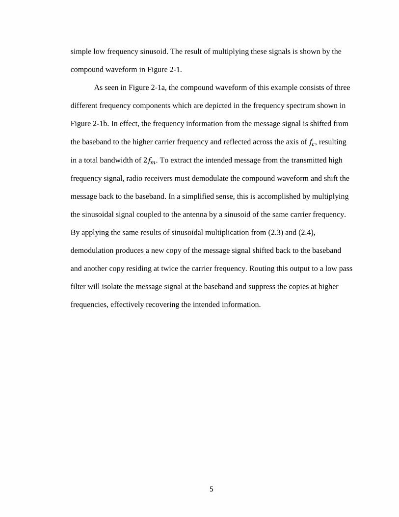
simple low frequency sinusoid. The result of multiplying these signals is shown by the
compound waveform in Figure 2-1.
As seen in Figure 2-1a, the compound waveform of this example consists of three
different frequency components which are depicted in the frequency spectrum shown in
Figure 2-1b. In effect, the frequency information from the message signal is shifted from
the baseband to the higher carrier frequency and reflected across the axis of 𝑓𝑐, resulting
in a total bandwidth of 2𝑓𝑚. To extract the intended message from the transmitted high
frequency signal, radio receivers must demodulate the compound waveform and shift the
message back to the baseband. In a simplified sense, this is accomplished by multiplying
the sinusoidal signal coupled to the antenna by a sinusoid of the same carrier frequency.
By applying the same results of sinusoidal multiplication from (2.3) and (2.4),
demodulation produces a new copy of the message signal shifted back to the baseband
and another copy residing at twice the carrier frequency. Routing this output to a low pass
filter will isolate the message signal at the baseband and suppress the copies at higher
frequencies, effectively recovering the intended information.

6
Figure 2-1a. Message Signal (Left), Carrier Signal (Right), and Compound Waveform
after Multiplication (Bottom).
Figure 2-1b. Frequency Representation of Compound waveform in 2-1a.
2.2 Super-Regenerative Oscillator & Review of Feedback
Like most radio receiver architectures, SRRs utilize a sinusoidal oscillator that is
set to oscillate at the carrier frequency of the received signal. The Super-Regenerative
Oscillator (SRO), also known as a positive feedback oscillator, is the defining component
of an SRR and governs the receivers operation and performance.

7
As seen in Figure 1-1, the basic structure of SRO oscillator consists of a
frequency selective network and an amplifier in a positive feedback configuration. The
frequency selective network is a band pass filter whose impulse and frequency response
are given in Figure 2-2.
Figure 2-2. (a) Impulse Response and (b) Frequency Response of Band Pass
Filter.
Physically this implies that in the presence of an applied impulse at the input, the tuned
circuit will ring at its resonant frequency characterized by the center frequency of the
filters passband. When there lacks a continued supply of energy to the network at its
resonant frequency, these oscillations will decay exponentially as the energy within the
network dissipates. By utilizing positive feedback, the decaying oscillatory response from
the initial excitation can be reinforced, allowing a constant level dictated by the feedback
gain.
When the selective network and amplifier are connected in a positive feedback
configuration, the relationship between each signal path is governed by
𝑣𝑜 = 𝐵𝑣𝑠 (2.5)
𝑣𝑎 = 𝐾𝑎𝑣𝑜 (2.6)
𝑣𝑆 = 𝑣𝑖𝑛 + 𝐾𝑎𝑣𝑜 (2.7)
8
where 𝐵 is the frequency response of the selective network. Rearranging these equations
allows us to relate the output of the system to its input by
𝑣𝑜 =𝐵
1−𝐾𝑎𝐵𝑣𝑖𝑛
=𝐵
1−𝐿𝑣𝑖𝑛
= 𝐻𝑣𝑖𝑛 , (2.8)
where 𝐿 is the open loop gain and 𝐻 is the closed loop gain of the system.
In practice, oscillator circuits are generators and thus have zero input (𝑣𝑖𝑛 = 0),
so it may not be initially obvious from (2.8) how such a circuit could start and sustain
oscillations. Theoretically for the system to oscillate with zero input, the closed loop gain
𝐻 must be infinite, implying that the open loop gain 𝐿 = 𝐾𝑎𝐵 must be real with zero
phase and unit magnitude. This requirement for steady oscillation is known as the
Barkhausen Criterion described in [13]. When the open loop gain is less than unity, the
oscillations in the circuit will eventually cease. Conversely, if the open loop gain is
greater than unity, the system becomes unstable and the oscillations will theoretically rise
to ever increasing levels. In practice however, non-linear characteristics of the gain
element cause the open loop gain to shift towards unity as the amplitude approaches a
maximum equilibrium value dependent on the gain element.
The distinguishing characteristic of SRRs is that their loop gain is manipulated
such that it varies periodically between levels that are higher and lower than unity.
Referring to Figure 1-1, the gain of the amplifier 𝐾𝑎 in the feedback path is controlled by
a time-varying “quench” signal. As the feedback gain varies proportionally with the
applied quench signal, the system alternates between states of stability and instability,
causing oscillations to build and decay (or quench) in correspondence with the gain level.
Thoughtful design of the receiver can allow for “self-quenching” in which the gain

9
element is automatically controlled, but for a manageable linear analysis of the system in
Section 3, it is assumed that the gain is controlled externally by an oscillating quench
signal with frequency 𝑓𝑞. In the presence of an RF input, the SRO outputs a series of RF
pulses with a period of 𝑇𝑞 = 1/𝑓𝑞 until the input signal ceases. In a sense, these pulses
can be viewed as “analog samples” of the received input signal.
SRRs have two modes of operation with respective advantages for different
communication and modulation schemes. In the linear-mode of operation, the oscillations
are damped before they reach their equilibrium amplitude characterized by the SRO
design. Thus, the level of the output pulses are proportional to the amplitude envelope of
the input signal, which is a desirable result for demodulating AM signals. Feeding these
pulses through a simple envelope detector and a low pass filter to remove the high
frequency quench component effectively demodulates the received signal. In the
logarithmic-mode of operation, the amplitude of the oscillations reaches its limit before
they are damped, resulting in a saturated output every cycle. In this scheme, the output
pulses are no longer proportional to the amplitude of the input envelope. Rather, the area
under the output pulse is proportional to the logarithm of the amplitude of the input. The
constant amplitude of pulses makes the logarithmic mode suitable for digital modulation
schemes such as PWM. Though the mathematical analysis presented in proceeding
sections focuses on the linear mode of operation, deeper analysis of the logarithmic mode
can be found in [1] and [11].

10
2.3 Detecting the SRO Output & Review of Demodulation
Upon reception of an AM signal that oscillates at the selective networks tuned
frequency, the SRR will output a series of evenly spaced high-frequency pulses with peek
amplitudes proportional to the message signal amplitude at that instance of time. Any
network connected to the receiver would only be interested in the information contained
in the message signal, and so the receiver must demodulate the signal by extracting the
message from its high frequency carrier.
To recover the message signal, we shall consider the very simple but popular
method of non-coherent envelope detection described in [9] and depicted in Figure 2-3.
Figure 2-3a. Simple Envelope Detector for AM Signals.
Figure 2-3b. Magnified View of Envelope Detector Output.

11
During the positive cycle of the input signal, the diode is forward-biased which
allows the capacitor to charge to the peak voltage of the input signal. As soon as the input
level drops below its peak, the diode becomes reverse-biased and acts as an open circuit.
The capacitor then discharges through the resistor at a slow rate with a time constant 𝜏 =
𝑅𝐶, slowly reducing the voltage across the capacitor. When the input signal becomes
positive with respect to the capacitor voltage, the diode is once again forward biased and
the process repeats.
In effect, the voltage across the capacitor roughly follows the envelope of the
input signal with a small amount of ripple of frequency 𝑓𝑐 due to the carrier wave. This
high frequency ripple can be reduced by increasing the time constant such that the
capacitor discharges less between positive cycles. However, increasing the time constant
too much will hinder the capacitors ability to accurately follow the envelope as can be
seen in Figure 5b. Thus, time constant 𝜏 should be large in comparison to 1/2𝜋𝑓𝑐 , but
small compared to 1/2𝜋𝐵𝑊 where 𝐵𝑊 is the highest frequency within the message
signal. Considering the RC network is simply a first order low-pass filter, higher-order
filtering of greater complexity can be employed to provide a steeper cutoff and further
minimize unwanted high-frequency ripple.

12
Chapter 3
Mathematical Analysis of the Classical SRR
This section offers a solution the characteristic equation of the SRR to be applied
to specific cases of operation in the following section. Additionally, this section defines a
new set of parameters that characterize the systems performance and simplify the
mathematical analysis of the solution. The proceeding mathematical derivations are based
on the results found in [1] and may be compared to an alternative state-space
representation of the system presented in [6] and [7].
3.1 Characteristic Equation of SRR
Since practical SRRs are non-linear devices, the mathematics describing their
operation makes numerous assumptions and approximations to linearize the equations
and present elegant and understandable results for different cases of operation. To begin
our mathematical approach, we shall assume that the SRO is operating in the linear mode.
The band pass network has a response centered at frequency 𝜔0 = 2𝜋𝑓0, characterized by
the generic second-order band pass transfer function:
𝐻𝑏𝑝𝑓(𝑠) = 𝐾0 ∗2𝜁0𝜔0𝑠
𝑠2+2𝜁0𝜔0𝑠+𝜔02 (3.1)
Converting this transfer function to the time domain produces the equivalent differential
equation
�̈�𝑜(𝑡) + 2𝜁0𝜔0�̇�𝑜(𝑡) + 𝜔02𝑣𝑜(𝑡) = 𝐾02𝜁0𝜔0�̇�𝑠(𝑡) (3.2)

13
where 𝐾0 denotes the maximum amplification of the network and 𝜁0 represents the
quiescent damping factor. Without feedback, the value of each variable is fixed and
dependent on the design of the filter. The output of the band pass filter is fed back to its
input establishing the relationship:
𝑣𝑠(𝑡) = 𝑣𝑖𝑛(𝑡) + 𝐾𝑎(𝑡)𝑣𝑜(𝑡). (3.3)
By substituting this expression for 𝑣𝑠(𝑡) into (3.1), we obtain the closed loop transfer
function and corresponding linear differential equation:
𝐻𝑆𝑅(𝑠, 𝑡) = 𝐾0 ∗2𝜁0𝜔0𝑠
𝑠2+2𝜁(𝑡)𝜔0𝑠+𝜔02 (3.4)
�̈�𝑜(𝑡) + 2𝜁0𝜔0�̇�𝑜(𝑡) + 𝜔02𝑣𝑜(𝑡) = 𝐾02𝜁0𝜔0[�̇�(𝑡) + 𝐾𝑎(𝑡)𝑣𝑜(𝑡)] (3.5)
�̈�𝑜(𝑡) + 2𝜁(𝑡)𝜔0�̇�𝑜(𝑡) + 𝜔02𝑣𝑜(𝑡) = 2𝜁0𝜔0�̇�(𝑡). (3.6)
When the loop is closed, the damping factor 𝜁 becomes a time-varying signal
𝜁(𝑡) = 𝜁0 ∗ (1 − 𝐾0 ∗ 𝐾𝑎(𝑡)) (3.7)
= 𝜁0 − 𝜁0𝐾0𝐾𝑎(𝑡) (3.8)
= 𝜁𝑑𝑐 + 𝜁𝑎𝑐(𝑡) (3.9)
This damping function plays a critical role in the design and analysis of super-
regenerative receivers, as many measurable and adjustable performance parameters are
dependent on it.
3.2 Damping Function
The time-varying damping function characterizes the systems sensitivity – and
thus, its oscillatory response – to an input signal. One damping cycle corresponds to one
quench cycle with a period of 𝑇𝑞 = 1/𝑓𝑞. Depending on the value of 𝜁(𝑡) during this
period, the system response can be undamped (|𝜁| = 0) underdamped (|𝜁| < 1),
critically damped (|𝜁| = 1), or over damped(|𝜁| > 1). Figure 3-1 from [12] depicts how

14
the pole-zero plot of the system is affected by a linearly decreasing damping function.
This shall be viewed as a single cycle of a saw tooth quench signal with a time interval
of [𝑡𝑎, 𝑡𝑏].
Figure 3-1. Effect of a Varying Damping Ratio on Pole-Zero Plot of SRO.
To demonstrate how the damping function affects the systems response in the
time domain, consider the sinusoidal damping function in Figure 3-2 from [1] with an
equivalently defined quench interval [𝑡𝑎, 𝑡𝑏]. As 𝜁(𝑡) approaches zero, the poles of the
system shift closer to the right half plane of the Laplace domain. The receiver is most
sensitive to input signals at this time and the presence of an input around this time will
cause an output response. When the damping function drops below zero, the poles cross
the imaginary axis into the right-half plane causing the system to become unstable.
Within the interval of the negative portion of the damping function [0, 𝑡𝑏], the system
gain increases significantly, causing an output pulse 𝑝𝑜(𝑡) to rise exponentially. Then, as
the damping factor undergoes the positive half cycle, the poles shift back towards the
left-hand plane, decreasing the systems sensitivity to an input while quenching the RF
energy buildup from the unstable portion of the cycle.

15
Figure 3-2: (a) Sinusoidal Damping function, (b) sensitivity and output curves, (c)
applied RF input pulse envelope.
If we define 𝑡𝑜 to be the time at which the damping function becomes negative,
we see that 𝜁𝐷𝐶 essentially dictates the amount of time the system is in a damped (𝑡𝑎 <
𝑡 < 𝑡0) and undamped (𝑡0 < 𝑡 < 𝑡𝑏) state. The longer the damping factor is positive, the
more time is allowed for the poles to sit in the left-hand plane to let the output
sufficiently decay before the next cycle. On the other hand, the negative portion of the
damping factor should be long enough to allow the output to rise to a sufficient signal
level for detection. In practice, any arbitrary wave function can be chosen so long as it
provides sufficient regeneration and quenching by having appropriately sized positive
and negative portions within each cycle.

16
3.3 Sensitivity
As previously mentioned, the value of 𝜁(𝑡) during a quench period dictates the
sensitivity of the receiver to an input signal. The level of sensitivity is inversely
proportional to the minimum received signal level necessary to generate an output, and
the width of the sensitivity envelope defines the duration for which the SRR is influenced
by that received excitation as explained in [10]. The level of sensitivity exhibits an
exponential dependence on the damping function, quantitatively expressed as
𝑠(𝑡) = 𝑒𝜔0 ∫ 𝜁(𝜆)𝑑𝜆𝑡
0 . (3.10)
The sensitivity of the receiver peaks at 𝑡 = 0 when the system is in an undamped state
and decreases exponentially as time departs from the origin on both sides. When an input
pulse 𝑝𝑖𝑛 occurs within this period of high sensitivity, an output pulse will occur at the
end of the cycle. The decaying portion of the output pulse envelope is described by the
equation:
𝑝𝑜(𝑡) = 𝑒−𝜔0 ∫ 𝜁(𝜏)𝑑𝜏
𝑡𝑡𝑏 . (3.11)
It should be noted that when sensitivity is high, even the smallest excitation such
as thermal noise of electrical components can push the system into oscillation, even when
there is no appreciable input signal present. However, the smaller the excitation, the
longer it will take for oscillations to build. Thus, the sensitivity period of the receiver
should be long enough to present sufficient gains in the presence of an input, but quick
enough to suppress the slower building oscillations due to electrical noise - A condition
that is dictated by the frequency of the applied quenching signal.

17
3.4 Solution of the Differential Equation
Assuming a linear mode of operation, the general solution to the second order
differential equation (6) can be represented as the sum of the homogenous and particular
solutions according to
𝑣𝑜(𝑡) = 𝑣𝑜𝐻(𝑡) + 𝑣𝑜𝑃(𝑡). (3.12)
The term 𝑣𝑜𝐻(𝑡) represents the natural (or free) response, which may exist without the
presence of an input, and 𝑣𝑜𝑃(𝑡) represents the forced response due to an input excitation.
3.4.1 Homogenous Solution: Free Response
To solve for the homogeneous response, we first set the input𝑣(𝑡) = 0, resulting
in the homogenous equation
�̈�𝑜𝐻(𝑡) + 2𝜁0𝜔0�̇�𝑜𝐻(𝑡) + 𝜔02𝑣𝑜𝐻(𝑡) = 0 . (3.13)
To simplify analysis, we make the following change of variable from 𝑣𝑜𝐻(𝑡) to 𝑢(𝑡)
𝑣𝑜𝐻(𝑡) = 𝑢(𝑡)𝑒−𝜔𝑜 ∫ 𝜁(𝜆)𝑑𝜆
𝑡𝑡𝑎 (3.14)
�̇�𝑜𝐻(𝑡) = (�̇� − 𝜔𝑜𝜁(𝑡) ∗ 𝑢)𝑒−𝜔𝑜 ∫ 𝜁(𝜆)𝑑𝜆
𝑡𝑡𝑎 (3.15)
�̈�𝑜𝐻(𝑡) = (�̈� − 2𝜔𝑜𝜁(𝑡)�̇� + [(𝜔0𝜁(𝑡))2
− 𝜔0𝜁̇(𝑡)] 𝑢) 𝑒−𝜔0 ∫ 𝜁(𝜆)𝑑𝜆
𝑡𝑡𝑎 , (3.16)
and substitute these expressions into the original equation. This substitution converts the
homogeneous equation into the Hill Equation as shown in [1]:
�̈�(𝑡) + 𝜔02 (1 − 𝜁2(𝑡) −
�̇�(𝑡)
𝜔0) 𝑢(𝑡) = 0. (3.17)
To simplify this equation and further analysis, we must satisfy two restrictions
imposed on the damping function:
𝜁2(𝑡) ≪ 1 (3.18)
|𝜁̇(𝑡)| ≪ 𝜔0. (3.19)

18
The first restriction implies that the instantaneous damping factor must be low enough
such that the system is underdamped and capable of generating an oscillatory response.
Considering the quality factor 𝑄 of the system where
𝑄(𝑡) =1
2𝜁(𝑡) , (3.20)
this restriction equivalently implies that the quality factor (or the frequency selectivity)
𝑄(𝑡) of the network must be kept high. As shown in Figure 3-3, a low quality factor
corresponds to a wide receiver bandwidth, making the system more susceptible to signals
and noise outside the bandwidth of interest.
Figure 3-3. Frequency response of a High-Q (Red) and Low-Q (Blue) System.
The second restriction implies that the damping factor must be slow varying compared to
the input RF frequency. Since the damping factor varies at a rate of 𝑓𝑞, this restriction
equivalently states that the quench frequency 𝑓𝑞 should be much lower than the center
frequency of the selective band pass network 𝑓0. Satisfying these two restrictions reduces
the Hill equation to:
�̈�(𝑡) + 𝜔02𝑢(𝑡) = 0. (3.21)

19
As can be seen, this representation of the system is linear with constant
coefficients unlike our original expression in (6). The solution to this equation will not be
derived in this paper, though it is known to be:
𝑢(𝑡) = 2𝑅𝑒[𝑉1𝑒𝑗𝜔0𝑡] = 𝑉1𝑒𝑗𝜔0𝑡 + 𝑉2𝑒−𝑗𝜔0𝑡. (3.22)
Substituting this expression (3.22) into (3.21) and reversing the change of variables made
in (3.14), (3.15), and (3.16) provides the general solution to the homogenous differential
equation:
𝑣𝑜𝐻(𝑡) = 𝑒−𝜔0 ∫ 𝜁(𝜆)𝑑𝜆
𝑡𝑡𝑎 ∗ 2𝑅𝑒[𝑉1𝑒𝑗𝜔0𝑡]. (3.23)
3.4.2 Particular Solution: Forced Response
To find the particular solution of the equation, we begin by using the method of
variation of parameters as described in [1]:
𝑣𝑜𝑃(𝑡) = 2𝑅𝑒[𝑉2(𝑡)𝑏(𝑡) + 𝑉2∗(𝑡)𝑏∗(𝑡) (3.24)
𝑏(𝑡) = 𝑒−𝜔0 ∫ 𝜁(𝜆)𝑑𝜆
𝑡𝑡𝑎 𝑒𝑗𝜔0𝑡 . (3.25)
According to the method of variation of parameters, the particular solution satisfies the
complete equation if
�̇�2𝑏 + �̇�2∗𝑏∗ = 0 (3.26)
�̇�2�̇� + �̇�2∗�̇�∗ = 2𝐾0𝜁0𝜔0�̇�. (3.27)
Solving this system of equations for �̇�2 yields the expression
�̇�2(𝑡) = −𝑗𝐾0𝜁0�̇�(𝑡)
𝑏(𝑡) . (3.28)
Integrating both sides of (3.28) provides an expression for 𝑉2
𝑉2(𝑡) = −𝑗𝐾0𝜁0 ∫�̇�(𝜏)
𝑏(𝜏)
𝑡
𝑡𝑎𝑑𝜏
= −𝑗𝐾0𝜁0 ∫ �̇�(𝜏)𝑡
𝑡𝑎𝑒
𝜔0 ∫ 𝜁(𝜆)𝑑𝜆𝜏
𝑡𝑎 𝑒−𝑗𝜔0𝜏𝑑𝜏 (3.29)

20
and by substituting (3.29) into (3.24), the expression for the particular solution is
obtained:
𝑣𝑜𝑃(𝑡) = 𝑒−𝜔0 ∫ 𝜁(𝜆)𝑑𝜆
𝜏𝑡𝑎 ×
2𝑅𝑒 [−𝑗𝐾0𝜁0 ∫ �̇�(𝜏)𝑡
𝑡𝑎𝑒
𝜔0 ∫ 𝜁(𝜆)𝑑𝜆𝜏
𝑡𝑎 𝑒−𝑗𝜔0(𝜏−𝑡)𝑑𝜏]. (3.30)
3.5 Redefining Gain for a Compact Expression of the Complete Solution
Though these solutions are complete, they don’t exactly offer an obvious
understanding of the systems operation. To offer a better interpretation of these
equations, we may re-write them as a product of several parameters that characterize the
systems performance while reducing the mathematical complexity of the solution.
As mentioned earlier, the gain of the overall system is dependent on the time-
varying damping function. The additional gain achieved by closing the loop is typically
separated into two parameters that are used to describe the performance of the receiver.
Since these gains arise from the positive feedback (or regeneration) of the closed loop,
they are referred to as the systems regenerative and super-regenerative gain.
The regenerative gain of the system 𝐾𝑟 is dependent on the DC component of the
damping factor, the frequencies of the received signal and tuned oscillator, and the area
of the input pulse envelope weighted by the sensitivity curve across one quench
interval [𝑡𝑎 , 𝑡𝑏]:
𝐾𝑟 = 𝜁0𝜔 ∫ 𝑝𝑖𝑛(𝜏)𝑠(𝜏)𝑑𝜏𝑡𝑏
𝑡𝑎. (3.31)
The more concentrated the input pulse energy is centered around peak sensitivity, the
higher the resulting regenerative gain. A wider input pulse of equal energy or a pulse
occurring away from peak sensitivity will result in a smaller regenerative gain. Note that
the expression in (3.31) assumes the input frequency matches the frequency of the

21
selective network. The dependence on 𝜔 shows that a greater number of received RF
oscillations within a quench cycle increases the regenerative gain. In other words, during
the high sensitivity period each successive RF cycle pushes the output envelop level
slightly higher. Thus, more RF cycles (higher frequency signal) within the sensitivity
period results in a larger regenerative gain.
The super-regenerative gain of the system 𝐾𝑠 is characterized by the exponential
growth of the oscillation and is determined by the area enclosed by the negative portion
of the damping function:
𝐾𝑠 = 𝑒−𝜔0 ∫ 𝜁(𝜏)𝑑𝜏𝑡𝑏
0 . (3.32)
Since 𝜁(𝑡) is negative within[0, 𝑡𝑏], evaluation of the integral produces a positive term in
the exponential, showing that 𝐾𝑟 is exponentially proportional to the systems period of
instability. One could also verify from (3.10) and (3.32) that 𝐾𝑠 is defined as the inverse
of the sensitivity curve 𝑠(𝑡).
It is worth noting that since these two parameters are dependent on the damping
function, they are inherently related to the periodic feedback gain 𝐾𝑎(𝑡). The total or
peak gain of the system is simply expressed the product of the three defined gains within
the system:
𝐾 = 𝐾0𝐾𝑟𝐾𝑠. (3.33)
With these new gain parameters defined, we may substitute them into (3.23) and (3.30) to
obtain the following homogenous and particular solutions in compact form:
𝑣𝑜𝐻(𝑡) = 𝑉ℎ𝑝(𝑡) cos(𝜔0𝑡 + 𝜙ℎ) (3.34)
𝑣𝑜𝑃(𝑡) = 2𝜁0𝐾0𝐾𝑠𝑝(𝑡) ∫ �̇�𝑖𝑛(𝜏)𝑠(𝜏) sin(𝜔0(𝑡 − 𝜏)) 𝑑𝜏𝑡
𝑡𝑎. (3.35)

22
𝑉ℎ and 𝜙ℎ are respectively related to the modulus and angle of the complex constant 𝑉1
introduced in Section 3.1 Now that the complete general solution to the characteristic
differential equation has been derived, specific cases related to the practical behavior and
performance of a super regenerative receiver can be easily analyzed.
3.5.1 SRR Response to an RF Pulse When Tuned to Carrier Frequency
In practical implementations, the receiver is designed to accept incoming RF
signals within the band of interest. With the complete solution clearly defined, we can
begin to analyze the case of an applied RF pulse in which the carrier frequency is equal to
the center frequency of the tuned band pass filter.
To start, it is assumed the RF pulse is applied within the interval of one quench
period [𝑡𝑎, 𝑡𝑏] with the expression
𝑣(𝑡) = 𝑉𝑝𝑖𝑛(𝑡) cos(𝜔𝑡 + 𝜙). (3.36)
The function 𝑝𝑖𝑛(𝑡) is the normalized envelope of the incoming RF pulse and V is its
peak amplitude. Ideally, 𝑝𝑖𝑛 = 0 outside of the defined quench period. Otherwise, a
fraction of the input signal received in one quench period will carry over into the next
quench period. In other words, the free response 𝑣𝑜𝐻 during the second quench period
will be non-zero, and thus the output will no longer be solely described by the forced
response to an input pulse within this period. The effects of a non-zero free response will
be explained in later sections, but for now we assume 𝑣𝑜𝑖(𝑡) = 𝑣𝑜𝑃𝑖(𝑡) for every 𝑖𝑡ℎ
quench period.
From (35), we see that the forced response 𝑣𝑜𝑃 is related to the derivative of the
input excitation, which is defined as

23
�̇�𝑖𝑛(𝑡) = 𝑉[�̇�𝑖𝑛(𝑡) cos(𝜔𝑡 + 𝜙) − 𝑝𝑖𝑛(𝑡)𝜔 sin(𝜔𝑡 + 𝜙)]. (3.37)
Assuming the input envelope varies slowly compared to its carrier oscillations
(|�̇�𝑖𝑛(𝑡)| ≪ 𝑝𝑖𝑛(𝑡)𝜔), we the input signal is approximated as
�̇�𝑖𝑛(𝑡) ≈ −𝑉𝑝𝑖𝑛(𝑡)𝜔sin (𝜔𝑡 + 𝜙). (3.38)
Since the free response 𝑣𝑜𝐻 is assumed be zero, the substitution of (3.38) into (3.30)
provides the output response of the system expressed as
𝑣𝑜(𝑡) ≈ −2𝑉𝜁0𝐾0𝐾𝑠𝜔𝑝(𝑡) ×
∫ 𝑝𝑖𝑛(𝜏)𝑠(𝜏) sin(𝜔𝜏 + 𝜙) sin(𝜔0(𝑡 − 𝜏)) 𝑑𝜏𝑡
𝑡𝑎. (3.39)
Since the input and sensitivity envelopes are slow-varying compared to 𝜔, the weight of
the high frequency component within the integral will be much lower than the low-
frequency component, allowing the approximation
𝑣𝑜(𝑡) ≈ −2𝑉𝜁0𝐾0𝐾𝑠𝜔𝑝(𝑡) ×
∫ 𝑝𝑖𝑛(𝜏)𝑠(𝜏) cos((𝜔 − 𝜔0)𝜏 + 𝜔0𝑡 + 𝜙) 𝑑𝜏𝑡
𝑡𝑎. (3.40)
Recall that the sensitivity curve 𝑠(𝑡) decreases rapidly as 𝑡 departs from the origin
on both sides, reaching negligibly small values outside of the sensitivity period [𝑡𝑠𝑎, 𝑡𝑠𝑏]
defined in Figure 3-2. Outside of this interval, one can assume the influence of an input
pulse on the output is very small. Assuming that 𝑠(𝑡) is small at the end of a quench
period, the effects of sensitivity on the output envelope and super-regenerative gain can
be seen by the expression
𝑠(𝑡𝑏) = 𝑝𝑜(0) = 𝑒𝜔0 ∫ 𝜁(𝜆)𝑑𝜆𝑡𝑏
0 =1
𝐾𝑠≪ 1. (3.41)

24
These relationships imply that a small sensitivity value at the end of a quench cycle (𝑡 =
𝑡𝑏), results in small output envelope values at 𝑡 = 0 and large super-regenerative gains.
This reiterates the fact that the output pulse from one cycle should be quenched before
the next high sensitivity period at 𝑡 = 0 + 𝑇𝑞 in the next cycle. With this satisfied, the
response is solely dictated by the input signal captured at that time, which is then
amplified at the end of the cycle 𝑡 = 𝑡𝑏.
Now, imposing the assumption that the receiver is tuned to the input carrier
frequency (𝜔 = 𝜔0), the approximate expression for the output (3.40) is simplified to
𝑣𝑜(𝑡) = 𝑉𝐾0𝐾𝑠𝑝𝑜(𝑡) [𝜁0𝜔0 ∫ 𝑝𝑖𝑛(𝜏)𝑠(𝜏)𝑑𝜏𝑡𝑏
𝑡𝑎] cos (𝜔0𝑡 + 𝜙) . (3.42)
Upon closer examination, we can see that factor contained in the brackets is the
expression for the previously defined regenerative gain 𝐾𝑟 (3.31), allowing an even
further simplified expression for the output:
𝑣𝑜(𝑡) = 𝑉𝐾0𝐾𝑟𝐾𝑠𝑝𝑜(𝑡) cos(𝜔0𝑡 + 𝜙)
= 𝑉𝐾𝑝𝑜(𝑡)cos (𝜔0𝑡 + 𝜙). (3.43)
3.5.2 SRR Response to an RF Pulse of Arbitrary Carrier Frequency
Until this point, it has been assumed that the carrier frequency of the input pulse is
equal to the tuned frequency of the SRO. To analyze the systems performance for an
arbitrary input carrier frequency, the regenerative gain and its dependence on the input
frequency must be considered. The general response to an excitation at an arbitrary
carrier frequency 𝜔 can then be given as
𝑣𝑜(𝑡) = 𝑉𝐾𝑝𝑜(𝑡) (𝜔
𝜔0) ∗
∫ 𝑝𝑖𝑛(𝜏)𝑠(𝜏)cos ((𝜔−𝜔0)𝜏+𝜔0𝑡+𝜙)𝑑𝜏𝑡𝑏
𝑡𝑎
∫ 𝑝𝑖𝑛(𝜏)𝑠(𝜏)𝑑𝜏𝑡𝑏
𝑡𝑎

25
= 𝑉𝐾𝑝𝑜(𝑡) (𝜔
𝜔0) ∗
𝑅𝑒[(∫ 𝑝𝑖𝑛(𝜏)𝑠(𝜏)𝑒𝑗(𝜔−𝜔0)𝜏𝑑𝜏)𝑒^𝑗(𝜔0𝑡+𝜙)𝑡𝑏
𝑡𝑎]
∫ 𝑝𝑖𝑛(𝜏)𝑠(𝜏)𝑑𝜏𝑡𝑏
𝑡𝑎
. (3.44)
By defining the complex function
𝜓(𝜔) = ∫ 𝑝𝑖𝑛(𝑡)𝑠(𝑡)𝑒𝑗𝜔𝑡𝑑𝑡∞
−∞
= 𝐹∗{𝑝𝑖𝑛(𝑡) ∗ 𝑠(𝑡)} (3.45)
where 𝐹[𝑥] represents the fourier transform of 𝑥, and utilizing the fact that the input
pulse 𝑝𝑖𝑛(𝑡) = 0 outside of the interval [𝑡𝑎, 𝑡𝑏], the output response can be re-written as
𝑣𝑜(𝑡) = 𝑉𝐾𝑝𝑜(𝑡) (𝜔
𝜔0)
𝑅𝑒[ 𝜓(𝜔−𝜔0)𝑒𝑗(𝜔0𝑡+𝜙)]
𝜓(0)
= 𝑉𝐾𝑝𝑜(𝑡) (𝜔
𝜔0)
|𝜓(𝜔−𝜔0)|
𝜓(0)cos (𝜔0𝑡 + 𝜙 + 𝜙𝜓) (3.46)
where 𝜙𝜓 is the angle of 𝜓(𝜔 − 𝜔0). By defining the frequency dependent component
of the above expression as
𝐻(𝜔) = (𝜔
𝜔0)
|𝜓(𝜔−𝜔0)|
𝜓(0), (3.47)
The output response can be condensed to the expression
𝑣𝑜(𝑡) = 𝑉𝐾𝑝𝑜(𝑡)|𝐻(𝜔)|cos (𝜔0𝑡 + 𝜙 + 𝜙𝐻). (3.48)
Note that for the case of an incoming RF pulse with carrier frequency 𝜔 = 𝜔0, the
magnitude and angle of the frequency dependent component 𝐻(𝜔) are 1 and 0°
respectively, resulting in a response identical to that of the received pulse in Section
3.5.1.
3.5.3 Response to a Sinusoidal Input
With the response to a single RF pulse defined, the case of a steady sinusoidal
input given as
𝑣𝑖𝑛(𝑡) = 𝑉𝑐𝑜𝑠(𝜔𝑡 + 𝜙) (3.49)

26
can be explored. To utilize the results from previous sections, this sinusoid can be viewed
as a sum of successive RF pulses occurring every 𝑚𝑡ℎ quench period,
𝑣𝑖𝑛(𝑡) = 𝑉 ∑ 𝑝𝑖𝑛(𝑡 − 𝑚𝑇𝑞)cos (𝜔(𝑡 − 𝑚𝑇𝑞) + 𝑚𝜔𝑇_𝑞∞𝑚=−∞ + 𝜙), (3.50)
where the pulse envelope 𝑝𝑖𝑛(𝑡 − 𝑚𝑇𝑞) is square with unit amplitude [8]. By utilizing
(3.48), the total response to (3.49) can be expressed as a superposition of single responses
to each 𝑚𝑡ℎ pulse:
𝑣𝑜(𝑡) = 𝑉𝐾|𝐻(𝜔)| ×
∑ 𝑝𝑜(𝑡 − 𝑚𝑇𝑞) cos(𝜔0𝑡 + 𝑚(𝜔 − 𝜔0)𝑇𝑞 + 𝜙 + 𝜙ℎ)∞𝑚=−∞ . (3.51)
3.6 Hangover
Recall that before this mathematical discussion began, it was assumed that the
response 𝑣0 to input pulse 𝑝𝑖𝑛 in a given quench cycle did not affect the response in the
next quench cycle. To achieve this ideality, the system must be sufficiently damped at the
beginning of a quench period to ensure any remaining energy from past periods is
extinguished. Thus, the output oscillation in a given quench cycle depends only on the
incoming signal within the sensitivity period of that quench cycle.
Hangover occurs when output oscillation in a given quench cycle is generated
from the remnant of the previous cycle. In other words, energy from the previous bit
“hangs over” into the next quench cycle. In digital communication schemes, a high level
of hangover will result in inter-symbol interference, thus increasing the bit-error rate. In
this case, the effects of appreciable hangover in the time domain result in a phenomenon
known as multiple resonance which affects the frequency response of the system. As the
amount of hangover increases, resonant peaks occurring at integer multiples of the

27
quench frequency become increasingly defined. Examples of these effects from [1] can
be seen in Figure 3-4 and Figure 3-5.
Figure 3-4. SRR Output Pulse Envelope for Different Hangover Percentages.
Figure 3-5. Effect of Hangover in the Frequency Response for Different Hangover
Percentages (Sinusoidal Steady State).

28
To quantify this behavior, the hangover coefficient is defined as the ratio between
the peak amplitudes of the second output pulse after time 𝑇𝑞 and that of the first output
pulse
𝑝𝑜(𝑡) = 𝑒−𝜔0 ∫ 𝜁(𝜆)𝑑𝜆
𝑡𝑡𝑏 = 𝑒−𝜔0𝜁𝐷𝐶(𝑡−𝑡𝑏)𝑒
−𝜔0 ∫ 𝜁𝐴𝐶(𝜆)𝑑𝜆𝑡
𝑡𝑏 (3.52)
ℎ =𝑝𝑜(𝑡𝑏+𝑇𝑞)
𝑝𝑜(𝑡𝑏)= 𝑒−𝜔0𝜁𝐷𝐶𝑇𝑞 = 𝑒
−2𝜋𝜁𝐷𝐶𝑓0𝑓𝑞 . (3.53)
The term 𝜁𝐷𝐶𝑇𝑞 is the area enclosed by the mean value of 𝜁(𝑡) in one quench cycle, or
more simply, the difference in area between the positive and negative portions of the
damping function. To minimize hangover, this difference should be maximized while still
retaining proper performance. To achieve this practically, compromises have to be made.
Raising the dc component of the damping function will reduce hangover but will
decrease the frequency selectivity of the system. On the other hand, lowering the quench
frequency increases the length of the sensitivity period, resulting in larger regenerative
gains that will push practical receivers outside their linear region of operation.
In practice, the quench rate is restricted to a minimum value dictated by the
maximum frequency of the modulating message signal. Considering the system is
essentially sampling the input every quench cycle, the quench frequency must be at least
twice the bandwidth of the modulating signal (𝑓𝑞 ≥ 2𝐵𝑊) to effectively capture the
signal information as given by the Nyquist Sampling Theorem. So, to reduce hangover at
a given quench frequency, 𝜁𝐷𝐶 must be increased to satisfy the following condition:
𝜁𝐷𝐶 > 𝑓𝑞
2𝜋𝑓0ln (
1
ℎ). (3.54)

29
Chapter 4
Simulation of the Classical SRR
4.1 Simulation Model
The block diagram in Figure 4-1 was created using Matlab’s Simulink program to
simulate the analytical results obtained in previous sections. This model contains all of
the components from our original diagram with the exclusion of the optional Low-Noise
Amplifier.
Figure 4-1. Simulink Model of SRR
The input to the SRR is an amplitude modulated sinusoid with frequency 𝑓𝑐 equal
to the tuned frequency of the filter 𝑓0, modulated by a random binary sequence with
bitrate 𝐵𝑅. The variable gain amplifier in the feedback loop is modeled simply as the
product of the output signal and a sinusoid oscillating at quench frequency 𝑓𝑞 with an
amplitude equal to the feedback gain 𝐾𝑎. From (3.7) we can derive the time-varying
damping function of the system as
𝜁(𝑡) = 𝜁0[1 − 𝐾0𝐾𝑎 sin(ωq𝑡)]. (4.1)

30
The output of the SRR is sent to a simple AM envelope detector circuit consisting of a
diode and 4th order Butterworth low pass filter for a steep roll-off at a cutoff frequency
higher than 𝑓𝐵𝑅 and lower than𝑓𝑞.
4.2 Simulation of Ideal SRR Operation
The design parameters for the ideal simulation and corresponding results are
given in Table 4-1 and Figure 4-2. Figure 4-2a shows the ideal amplitude modulated
input signal. Received signals in practice are of much lower amplitude, but under
appropriate operating conditions the receiver response will be similar to the simulation
results on a per unit basis. The output of the SRR is shown in Figure 4-2b. The peeks in
the waveform are a result of the damping function reaching an undamped state allowing
oscillations to rise. Comparing (a) to (b) it is seen that the overall gain of the SRR is
roughly 4.5 V/V – quite low for typical SRR implementations. With careful observation
of (4.1), the damping function never actually reaches a value below zero when both 𝐾0
and 𝐾𝑎 are unity, implying from (3.32) that the super-regenerative gain of the system is
also unity. This implies that the overall gain increase of this simulation is dictated solely
by the regenerative gain 𝐾𝑟. Much higher gains are achievable with small increases to 𝐾0
or 𝐾𝑎 that allow the damping function to reach a negative value and are in fact necessary
for typically low amplitude input signals.

31
Table 4-1. Parameters for Ideal SRR Simulation.
Figure 4-2. Simulation of Ideal SRR: (a) RF Input (b) SRO Output (c) Envelop Detector.
Variables Sym Value
Sample Frequency 𝑓𝑠 10 MHz
Tuned Frequency of BPF 𝑓0 1 MHz
Carrier Frequency 𝑓𝑐 1 MHz
Quench Frequency 𝑓𝑞 40 KHz
Bit Rate 𝐵𝑅 10 Kb/s
Damping Ratio 𝜁0 .1
Open Loop Filter Gain 𝐾0 1
Feedback Gain 𝐾𝑎 1
Input Voltage V 1 V

32
Figure 4-3. Simulation Results Given: Ko=1.5, Ka = 1 (Left) and Ka= 1.5, Ko = 1
(Right).
4.3 Multiple Resonance Due to Increasing Quench Frequency
The following results in Figure 4-4 demonstrate the effects on the frequency
response of the system in the sinusoidal steady state by raising the quench frequency
while keeping all other parameters constant. Figure 4-4a is the frequency response of our
original simulation. Figure 4-4(b-d) are the resulting frequency responses from increasing
the quench frequency. As expected, the gain decreases as the quench frequency increases
due to the lower amount of high frequency RF cycles within a single quench period. It is
also apparent that increasing the quench frequency while keeping the DC component of
the damping function constant accentuates the multiple resonance effect due to hangover
discussed in section 3.4. Each resonant peak occurs at an integer multiple of the quench
frequency away from the tuned center frequency of the system.

33
Figure 4-4. Example of Multiple Resonance: (a) 𝑓𝑞 = 40 𝐾𝐻𝑧 (Top Left), (b) 𝑓𝑞 =
80 𝐾𝐻𝑧 (Top Right), (c) 𝑓𝑞 = 160 𝐾𝐻𝑧 (Bottom Left), (d) 𝑓𝑞 = 320 𝐾𝐻𝑧 (Bottom
Right).
4.4 Hangover Due to Reducing the Quiescent Damping Factor
Figure 4-5 consists of two simulations that demonstrate the hangover effect due to
a reduction of the quiescent damping factor 𝜁0. The response in (a) is an expected output
for a system whose damping factor is kept high enough such that the oscillations are
adequately quenched. The response after decreasing 𝜁0 by a factor of 2 while keeping all
other parameters constant is shown in (b). First note that this results in a significant gain
reduction, as both regenerative and super-regenerative gains are exponentially related to

34
the area enclosed by one cycle of the damping function. This reduction also drastically
effects the system’s ability to extinguish oscillations after an RF input ceases. If this
single pulse was instead a digital bit stream or a series of pulses, the hangover in (b)
would cause the comparator portion of the detector to falsely output a logical HIGH value
despite receiving a logical LOW input at that instance of time.
Figure 4-5. SRR response to an input RF pulse given a high (left) and low (right)
quiescent damping factor.
4.5 Simulation with an Amplitude Modulated Input Signal
The simulations in this section are intended to provide a closer representation to
the practical design that will be proposed in Chapter 5. To mimic the electrical limitations
of the time-varying gain element used in the practical design, a saturation block was
inserted before multiplication that clips the quench signal for values larger than +/-

35
50mV. Since the feedback gain can no longer be controlled by arbitrary quench signal
values (which previously corresponded to 𝐾𝑎), two amplifiers with gains of 10 V/V were
added to the feedback path and at the SRO output to compensate for the gain reduction.
These modifications to the original simulation model are shown in Figure 4-6.
Figure 4-6. Modified SRR Model.
The input signal is a noisy AM waveform obtained from the product of a 20 KHz
sinusoidal message signal of 500mVac with a 1Vdc bias and a 1 MHz, 100mVac carrier
wave. These values were chosen to represent a typical AM input signal at the maximum
audible frequency that a practical SRR may receive, demonstrating its suitability for
receiving continuous AM audio signals.
Two simulations were conducted using different quench signal amplitudes to
demonstrate the linear and saturated operating modes of the practical time-varying gain
element. The first simulation shown in Figure 4-7 is resultant of a 60 KHz, .05Vac
sinusoidal quench signal controlling the feedback gain of the SRO. In this case, the
sinusoidal quench signal controls the gain linearly as it did in previous simulations. From
top to bottom, the graphs in Figure 4-7 depict the input AM waveform, the output of the
SRO and the output of the envelope detector with a low pass filter cutoff frequency of 25
KHz.

36
Figure 4-7. SRR Simulation with an AM Input Signal and Linear Gain Control: (a) AM
Input Signal (Top), (b) SRO Output (Center), (c) Envelope Detector Output (Bottom).
The second simulation shown in Figure 4-8 is resultant of a 60 KHz, .2Vac sinusoidal
quench signal that exceeds the imposed 50mV saturation limit of the gain element. The
clipping of this control signal results in the square wave damping function depicted in the
upper plot of Figure 4-8. The center and bottom plots again depict the SRO output and
envelope detector output respectively.

37
Figure 4-8: SRR Simulation with an AM Input Signal and Saturated Gain Control: (a)
damping function (top), (b) SRO Output (Center), Envelope Detector Output (Bottom).
Not only do these simulations demonstrate the SRRs ability to demodulate practical
continuous signals, but they also prove that both sinusoidal and square quench signals
(and thus, sinusoidal and square damping functions) can be used to control the feedback
gain of the SRR with similar results. This fact reiterates the comments made in Section
3.2 that the shape of the damping function is arbitrary so long as the system is designed to
have appropriate durations of sensitivity, regeneration and quenching.

38
Chapter 5
Electrical Model & Practical Implementation
5.1 Electrical Model
Now that a strong mathematical understanding of SRR operation has been
established, the generic results of previous sections can be easily applied to an electrical
model. Figure 5-1 presents the most common electrical representation to model super-
regenerative operation.
Figure 5-1. Electrical Model of a Super-Regenerative Receiver.
This circuit is simply an LC tank circuit with an added conductance 𝐺 that models the
tank’s resistive losses, and a time-varying negative conductance 𝑔 in parallel with the
tank’s inherent conductance. The RF current source 𝑖(𝑡) represents incoming external RF
signals induced in the tank, which can be thought of as the signal from a receiving
antenna represented as
𝑖(𝑡) = 𝐴(𝑡)𝑠𝑖𝑛(𝜔0𝑡). (5.1)

39
Since we are interested in the operation of the receiver when it is tuned to the input
carrier frequency, we shall assume that 𝜔𝑐 ≈ 𝜔0 = √1
𝐿𝐶 as defined in [5].
When the switch is open (𝑡 < 0), the voltage across the tank takes on the
expression
𝑣(𝑡) = 𝑣𝑜𝑘𝑒−𝑡𝐺
2𝐶 ∗ sin(𝜔0𝑡). (5.2)
When the switch closes (𝑡 ≥ 0), the negative conductance 𝑔 is added to the tanks
quiescent conductance 𝐺. To simplify the analysis, we shall assume that the total
conductance of the network is equal to some positive value G when the switch is open,
and some new negative value – 𝑔 when the switch is closed. Once the switch is closed,
the equation describing the circuit via KCL is
𝐶�̇� + 𝑔𝑣 +1
𝐿∫ 𝑣𝑑𝑡
𝑡
0= 𝑖(𝑡). (5.3)
The solution in terms of the tank voltage is then given as
𝑣(𝑡) = 𝑣𝑜𝑘𝑒+𝑡𝑔
2𝐶 ∗ 𝐴(𝑡)sin (𝜔0𝑡) (5.4)
𝜔0 = √ 1
𝐿𝐶+ (
𝑔
2𝐶)
2
(5.5)
As can be seen from (5.4) when the negative conductance is introduced the
voltage across the tank is sinusoidal with an exponentially increasing amplitude envelope.
Relating this to the generic closed loop model, the damping factor of this system at this
particular instant is less than or equal to 0, meaning the system is undamped and the
amplitude of oscillations will rise to ever-increasing levels due to positive feedback. In
practical cases, non-linearities of oscillatory circuits will cause the amplitude to level off
over time, making the network a steady oscillator of constant amplitude. However, for the
purposes of this example it is assumed that the switch will open before the oscillations

40
reach a steady amplitude, thus preserving the receivers’ linear mode of operation. It
should be noted from (5.4) that introducing a negative conductance will shift the center
frequency of the band pass network, and so the magnitude of this additional term should
be kept small enough to minimize its effects on the center frequency.
When the switch opens again, the voltage across the tank reverts back to a
decaying sinusoid approaching 0V. Since the state of the switch is dictating weather the
network is overdamped (open) or undamped (closed), this hard switching scheme is
equivalent to a square wave quench signal controlling the feedback gain of our generic
model, alternating the network between stable and unstable states. The switching period
is equivalent to the quench period of the quench oscillator (and thus, the period of the
time-varying feedback gain). With this in mind, the switching action of this band pass
network can be modeled as a time-varying conductance in parallel with the networks
inherent conductance.
Figure 5-2. Electrical Model with a Time-Varying Conductance.
From this form, all of the general parameters from Chapter 3 can be mapped to equivalent
electrical parameters which would provide the same mathematical results from an
electrical perspective as shown in [10] and [12]. Mappings of these parameters are given
in Table 5-1.

41
Block Diagram Electrical Model
Input Signal 𝑣𝑖𝑛 𝑖
Output Signal 𝑣𝑜 𝑣𝑜
Tuned
Frequency 𝜔0
1
√𝐿𝐶
Filter Gain 𝐾0 𝑍0 =1
𝐺0
Damping Ratio 𝜁0 1
2𝑅0𝐶𝜔0
=1
2𝑄0
=𝑍0
2𝑅
Feedback Gain 𝐾𝑎(𝑡) 𝐺𝑎(𝑡)
Damping
Function 𝜁(𝑡) = 𝜁0[1 − 𝐾𝑎(𝑡)𝐾0] 𝜁(𝑡) = 𝜁0[1 − 𝐺𝑎(𝑡)𝑍0]
Table 5-1. Parameter Mappings for the Equivalent Electrical Model
5.2 Self-Quenching
As mentioned earlier, quenching can be achieved externally with an oscillator
controlling the feedback gain, or by designing the band pass network to allow for “self-
quenching.” In fact, a large reason why supper-regenerative receivers were popular in the
earlier years of communications was because non-linear characteristics of a single device
(transistor or tube) could be exploited to detect and perform self-quenching at the same
time, reducing the cost and size of the circuit (an attractive benefit considering the size of
transistors and tubes at the time).In practice, the transistor acts as a nonlinear negative
resistance, providing the oscillatory response described for the simple RLC circuit above.
5.3 Colpitts Oscillator
As a practical example, the single-transistor SRR design presented in [5] shall be
considered. The core of the receiver discussed in [5] is based on the simple yet popular
Colpitts oscillator shown in Figure 6-3. The gain element is a bipolar transistor amplifier
in a common emitter configuration. Rb1 and Rb2 bias the transistor. Resistor 𝑅𝑐 limits

42
the collector current of the transistor. Capacitors 𝐶𝑖𝑛 and 𝐶𝑜𝑢𝑡 act as decoupling
capacitors to separate and remove the DC component of the AC signal. Capacitor 𝐶𝑒 acts
as an emitter bypass capacitor that prevents the amplified AC from dropping across 𝑅𝑒.
Without it, the AC signal will drop across 𝑅𝑒 and alter the DC biasing conditions of the
Amplifier.
Figure 5-3. Colpitts Oscillator.
The output at the collector is fed back to the base with a resonant LC tank circuit in the
feedback loop. The two capacitors in the tank form a single “tapped” capacitor whose
total effective capacitance is determined by
𝐶𝑡𝑜𝑡𝑎𝑙 =𝐶1𝐶2
𝐶1+𝐶2 (5.6)
When the power is switched on, the capacitors in the tank start charging. When
fully charged, they start to discharge through the tanks inductor L. When the capacitors
fully discharge, the stored electrostatic energy is transferred as magnetic flux through the

43
inductor. Once the inductor starts discharging its energy, the capacitors charge up again.
The energy transfer between these elements form the basis of the circuits oscillation. The
frequency of oscillation is characterized by the equation
𝑓 =1
2𝜋√𝐿𝐶𝑡𝑜𝑡𝑎𝑙 (5.7)
In a passive tank circuit, these oscillations will eventually die out as the reactive elements
reach steady state equilibrium. To sustain oscillations, the lost energy is compensated by
the common-emitter transistor amplifier. This amplifier configuration takes an input
signal at the base and outputs a scaled version of the signal shifted 180° at the collector
output. Grounding the connection between C1 and C2 results in equal voltages of
opposite polarity across the two elements, thus introducing another 180° phase shift such
that the feedback signal is in-phase with the input. The resulting positive feedback
sustains the oscillations at an amplitude level characterized by component values of the
amplifier. The author of [5] modifies the base-emitter junction of this steady oscillator
with an added RLC circuit to achieve time-varying gain resulting in self-quenching
operation.
5.4 Alternative Time-Varying Gain Element
The initial goals for the practical design offered in this section were focused on
modifying the single-transistor Colpitts oscillator to achieve self-quenching operation
with minimal additional components, all while maintaining suitable performance within
the AM frequency range. Unfortunately, the non-linear gain control of the single-
transistor design could only be partially described by the analysis presented in Chapter 3.
To conclude the concepts and analysis of this report, this section presents a practical

44
implementation that utilizes a monolithic IC package to realize the time-varying gain
element of the SRO model. Though this modification sacrifices cost efficiency, it allows
for a circuit realization that is closely related to the simulation model presented in Section
4.
Much like the simulation model, this circuit consists of a selective network whose
output is fed back to an MC1496 monolithic balanced modulator which is configured to
act as the externally controlled amplifier in
Figure 1-1. The schematic for the MC1496 is shown in Figure 5-4. The design consists
of a differential amplifier (Q5-Q6) that drives a dual differential amplifier pair (Q1-Q2,
Q3-Q4). Transistors Q7 and Q8 and connecting bias circuitry form two DC current
sources to provide proper biasing of the lower differential pair. This circuit topology is
identical to the four-quadrant multiplier discussed in [13], and is characterized by its
ability to deliver an output that is proportional to the product of two input signals. As a
four-quadrant multiplier, the MC1496 permits multiplication of both positive and
negative input signals, making it an effective building block for numerous RF
applications of varying complexity. The schematic shown in Figure 5-5 is a simplified
model to demonstrate and analyze the performance of a four-quadrant multiplier. Note
that the additional emitter and load resistors 𝑅𝐸 and 𝑅𝐿 are external components used to
set the appropriate device voltage gain for the design application.

45
Figure 5-4. Schematic of MC1496 Balanced Modulator.
Figure 5-5. Analysis Model for the MC1496.
Analysis of the multiplier circuit is based on the assumption that the BJT pairs are
matched and have negligible base currents. Under this assumption, the following
expressions for the branch currents can be defined:
𝐼1 = 𝐼5 ≡ 𝐼𝑏𝑖𝑎𝑠 (5.8)

46
𝐼𝑦 =𝑉𝑦
𝑅𝐸 (𝑅𝐸 ≫ 𝑟𝑒) (5.9)
𝐼2 =(𝐼1+𝐼𝑦)
1+𝑒𝑉𝑥𝑎
, 𝐼3 =(𝐼1+𝐼𝑦)
1+𝑒−
𝑉𝑥𝑎
𝐼4 =(𝐼1−𝐼𝑦)
1+𝑒−
𝑉𝑥𝑎
, 𝐼5 =(𝐼1−𝐼𝑦)
1+𝑒𝑉𝑥𝑎
} (5.10)
Where
𝑎 =𝑘𝑇
𝑞 .
(5.11)
Currents 𝐼𝐴 and 𝐼𝐵 can be represented as sums of these collector currents,
𝐼𝐴 = 𝐼2 + 𝐼4 =(𝐼1+𝐼𝑦)
1+𝑒𝑚 +(𝐼1−𝐼𝑦)
1+𝑒−𝑚
𝐼𝐵 = 𝐼3 + 𝐼5 =(𝐼1+𝐼𝑦)
1+𝑒−𝑚 +(𝐼1−𝐼𝑦)
1+𝑒𝑚
} (5.12)
where 𝑚 = 𝑉𝑥
𝑎. Taking the difference between Currents 𝐼𝐴 and 𝐼𝐵 as derived in [14] yields
𝐼𝐴 − 𝐼𝐵 =2𝐼𝑦(𝑒−𝑚−𝑒𝑚)
(1+𝑒𝑚)(1+𝑒𝑚). (5.13)
The differential voltage between the two load resistors is then given as
∆𝑉𝑜 = 𝑅𝐿2𝐼𝑦(𝑒−𝑚−𝑒𝑚)
(1+𝑒𝑚)(1+𝑒𝑚) . (5.14)
Combining (5.9) with (5.14) and substituting 𝑉𝑥
𝑎 back into the equation forms for the
complete expression for the voltage gain from the differential output to input 𝑉𝑦
∆𝑉𝑜
𝑉𝑦=
2𝑅𝐿
𝑅𝐸
(𝑒−
𝑉𝑥𝑎 −𝑒
𝑉𝑥𝑎 )
(1+𝑒𝑉𝑥𝑎 )(1+𝑒
−𝑉𝑥𝑎 )
= −2𝑅𝐿
𝑅𝐸tanh (
𝑉𝑥
2𝑎) (5.15)
From this expression it can be seen that the voltage gain is a non-linear function of the
input signal applied to the upper two differential pairs. The hyperbolic tangent function in
(5.15) is approximately linear for argument values close to zero and levels off to +/- 1 as
the argument departs further from zero. A large sinusoidal control voltage would appear

47
as a square wave periodically changing the sign of the input voltage. Alternatively, a low
voltage control signal can be used to vary the voltage gain linearly, causing the multiplier
to act as a variable gain amplifier. The amplitude limits imposed on the applied control
voltage signal for linear operation are further defined in [14], though the typical range is
+/- 50mV.
Figure 5-6. Balanced modulator configuration.
Figure 5-6 depicts the typical configuration for the balanced modulator as
provided by the MC1496 datasheet [14]. The gain element of the SRO will be
implemented using this configuration with a few changes to the defined inputs. The
output voltage 𝑣0 of the selective network will be fed into input 𝑉𝑆 (𝑉𝑦) and the external
quench signal 𝑣𝑞 will be applied to input 𝑉𝑐 (𝑉𝑥). The differential output of the MC1496
will feed into a differential amplifier, converting it into a single ended signal to be fed
back to the selective network input.

48
5.5 Proposed Design & Implementation
The schematic of the proposed SRR design for circuit simulation is shown in
Figure 5-7. Three voltage sources fed into an operational amplifier are used to model a
300mV AM signal with a carrier frequency of 1 MHz and message frequency of 20 KHz.
The band pass filter is composed of the simple LC tank that is used as the selective
network for the Colpitts oscillator. The variable gain amplifier mimics the MC1496
circuit schematic in Figure 5-4 with the appropriate connections for a balanced modulator
as given in Figure 5-6. The applied quench signal to the MC1496 is a 50mV sinusoid
with a frequency of 120 KHz. 60 KHz was sufficient for the ideal model simulated in
Matlab, however this frequency did not provide sufficient quenching in the practical
design. The differential output is fed into a differential amplifier to provide voltage gain
and convert the output to a single ended voltage signal which feeds back to the selective
network. The peak detector circuit is designed to have a time constant sufficient for
reasonable tracking of the output envelope and is cascaded with a low pass filter with a
cutoff frequency of around 30 KHz to reduce the rippling effect from the quenched
output pulses.

49
Figure 5-7. Schematic of the Practical SRR Implementation
The simulation results of this circuit are shown in Figures 5-8. The blue and red
signals in Figure 5-8a are the input AM signal and the output of the amplifier in the
feedback loop respectively. The quenching action of the feedback amplifier becomes
apparent after 200𝜇𝑠 as the pulses occurring every 𝑇𝑞 seconds become more defined.
Figure 5-8b is a magnified view of 5-8a starting at 200𝜇𝑠 to provide a clearer view of the
output pulses. Figure 5-8c depicts the output of the peak detector circuit compared to the
input signal. As can be seen, the peak detector accurately tracks the quenched output
pulses and successfully extracts the 20 KHz message signal from the modulated carrier
with a 500mVdc offset.
AM Signal Generator
Peak Detector + LPF
Selective Network
Variable Gain Amplifier

50
Figure 5-8. (a) Feedback Amplifier Output (Top), (b) Magnified View of Feedback
Amplifier Output (Center), (c) Peak Detector Output (Bottom).

51
5.6 Physical Implementation
A physical prototype of the simulated design is given in Figure 5-9. The selective
network and MC1496 are configured as they were in the simulation, however some minor
adjustments were made to account for the non-idealities of the practical op-amp used to
amplify the feedback signal after multiplication. Instead of sending both outputs of the
MC1496 to a differential amplifier, this circuit feeds a single-ended output to a pair of
cascaded HA-2515 op-amps in non-inverting configuration. The HA-2515 has a gain-
bandwidth product of 12 MHz which is higher than typical operational amplifiers.
However, a considerable amount of amplification was needed to boost the low-voltage
single-ended signal from the balanced modulator. The cascaded design ensures sufficient
amplification for peak detection can be achieved while still preserving the integrity of the
signal.
Figure 5-9. Prototype of the proposed SRR design.

52
The results of this circuit configuration are shown in Figure 5-10. The input signal
is a 300mVac 1 MHz AM signal modulated by a 20 KHz message signal. The quench
signal is a 60mVac sinusoid with a frequency of 120 KHz. Like the simulated design, a
quench frequency of 60 KHz did not extinguish the building oscillations sufficiently,
which compromised the envelope of the 20 KHz message signal. The 150mV signal in
Figure 5-10a is the single-ended output of the MC1496. The quenched pulses in the
output waveform are comparable to those shown in Figure 5-8. This signal was fed into
two cascaded non-inverting op-amps, each providing a gain of roughly 5.2 V/V using 39
KOhm and 8.2 KOhm resistors. The feedback signal before and after amplification is
compared in Figure 5-10b by the yellow and blue signals respectively. The 4V signal
after amplification is sent to the peak detector circuit previously discussed in Section 2.3
which is cascaded with a low pass filter. The parallel configuration of the 1nF capacitor
and 18.9 KOhm has a time constant of 18.9𝜇𝑠 (52.9 KHz) which allows the peak detector
the track the envelope of the 120 KHz output pulses effectively. The passive RC low pass
filter has a cutoff frequency of 100 KHz to remove some of the ripple caused by the high
frequency pulses. A comparison of the amplified feedback signal and the output signal of
the peak detector is given in Figure 5-10c. As can be seen, the SRR circuit successfully
demodulates the 1 MHz AM signal and outputs the extracted 20 KHz message signal.
Depending on the requirements of the application, further amplification and higher order
filtering can be implemented after demodulation to boost the signal strength and improve
the integrity of the sinusoid.

53
Figure 5-10. (a) Output of MC1496, (b) feedback signal before and after amplification,
(c) peak detector output compared to amplified feedback signal.

54
Chapter 6
Conclusions & Future Work
Despite their age, Super-Regenerative Receivers have proven to be resilient
options for RF reception in applications where low-power consumption, architecture
simplicity and cost efficiency are desired. This study has successfully presented a
mathematical understanding of SRR operation and working implementation to
demonstrate the theoretical results. Though the final design deviated from the initial goal
of minimizing cost and complexity, it boasts an architecture that is easily relatable to the
generic model that has been used to understand SRR operation for decades. The generic
mathematical analysis and the easily relatable practical implementation can be used as a
springboard for improved SRR architectures designed for specifically for various
communication applications.
Future work will focus on integrating the self-quenching action described in
Chapter 6 into the current design. The intent of this modification is to allow for optimal
quenching frequencies across a range of desired carrier frequency inputs without the need
for an externally controlled oscillator. This improvement would benefit commercial radio
receivers that are expected to operate consistently across numerous frequency bands in
the AM and FM range.
With the increasing relevance of short range communications for RFID and
sensor network applications, integrating the proposed design into a single package via
CMOS technology is also worth considering. Such applications include the Internet of
Things, home automation and remote control operation of consumer devices. The design
of sensors and RFID tags is highly focused on minimizing the size and power of the

55
device so that they are non-intrusive and have a long battery life. These devices typically
do not require high-level performance, making the SRR a highly affordable option for the
intended communication purposes. Integrating the proposed design into a smaller
package would make for an attractive option as the need for smaller, long-lasting RF
communication devices continues to grow.

56
References
[1] Moncunill-Geniz, F., Pala-Schonwalder, P., & Mas-Casals, O. (2005). A generic
approach to the theory of superregenerative reception. IEEE Transactions on Circuits
and Systems I: Regular Papers, 52(1), 54-70
[2] Vouilloz, A., Declercq, M., & Dehollain, C. (n.d.). Selectivity and sensitivity
performances of superregenerative receivers. ISCAS 98. Proceedings of the 1998
IEEE International Symposium on Circuits and Systems.
[3] Lee, D., & Mercier, P. P. (2017). Noise Analysis of Phase-Demodulating
Receivers Employing Super-Regenerative Amplification. IEEE Transactions on
Microwave Theory and Techniques.
[4] Hernandez, L., & Paton, S. (n.d.). A superregenerative receiver for phase and
frequency modulated carriers. 2002 IEEE International Symposium on Circuits and
Systems. Proceedings.
[5] Insam, E. (april 2002). Designing Super-Regenerative Receivers. Electronics
World.
[6] Frey, D. R. (2013). Improved Super-Regenerative Receiver Theory. IEEE
Transactions on Circuits and Systems.
[7] Frey, D. (2006). Synchronous filtering. IEEE Transactions on Circuits and
Systems.
[8] Pala-Schonwalder, P., Moncunill-Geniz, F. X., Bonet-Dalmau, J., Del-Aguila-
Lopez, F., & Giralt-Mas, R. (2009). A BPSK superregenerative receiver. Preliminary
results. 2009 IEEE International Symposium on Circuits and Systems.
[9] Lathi, B. P. (2016). Signal processing and linear systems. New York: Oxford
University Press.4]
[10] Thoppay, P. E., Dehollain, C., & Declercq, M. J. (2008). Noise analysis in super-
regenerative receiver systems. 2008 Ph.D. Research in Microelectronics and
Electronics.
[11] Feick, R., & Rojas, O. (1997). Modeling and simulation of the superregenerative
receiver. IEEE Transactions on Consumer Electronics.
[12] Bonet-Dalmau, J., Moncunill-Geniz, F. X., Pala-Schonwalder, P., Aguila-Lopez,
F. D., & Giralt-Mas, R. (2012). Frequency Domain Analysis of Superregenerative
Receivers in the Linear and the Logarithmic Modes. IEEE Transactions on Circuits
and Systems.
[13] Franco, S. (2015). Design with operational amplifiers and analog integrated
circuits. New York: McGraw-Hill.
[14] ON Semiconductor (October, 2006). Balanced Modulators/Demodulators.
MC1496.

57
Biography
Anthony Evelina was born on November 19th, 1993. He lives in Caldwell, New
Jersey with his parents Darlene and Robert Zalewski, and his grandmother Marie
Lanfrank. Anthony attended Montclair Kimberley Academy from kindergarten until his
high school graduation in May 2012. After graduation, he attended Lehigh University to
pursue a degree in Electrical Engineering. After graduating with a B.S. in Electrical
Engineering in May 2016, he continued his studies at Lehigh to work towards a M.S. in
Electrical Engineering and is expected to complete the requirements by December 2017.
During his time as a graduate student, Anthony served as a Teacher’s Assistant for the
2016-17 ECE 258 Senior Design Class and as an Adjunct Lecturer for the ECE 182
Junior Lab in the summer of 2017. Outside of engineering, Anthony has enjoyed playing
the guitar for ten years and he has actively performed with two jazz bands at Lehigh
University.