The XL16 Processor - School of Computingfivas/cs3710/TheXL16Processor2.doc · Web viewsets the...
71
Transcript of The XL16 Processor - School of Computingfivas/cs3710/TheXL16Processor2.doc · Web viewsets the...

The
XL16 Microproc
essor

The XL16 Microprocessor
http:\\www.cs.utah.edu\~fivas\cs3710
Page 2 of 52

The XL16 Microprocessor
Page 3 of 52
The XL16 Microprocessor
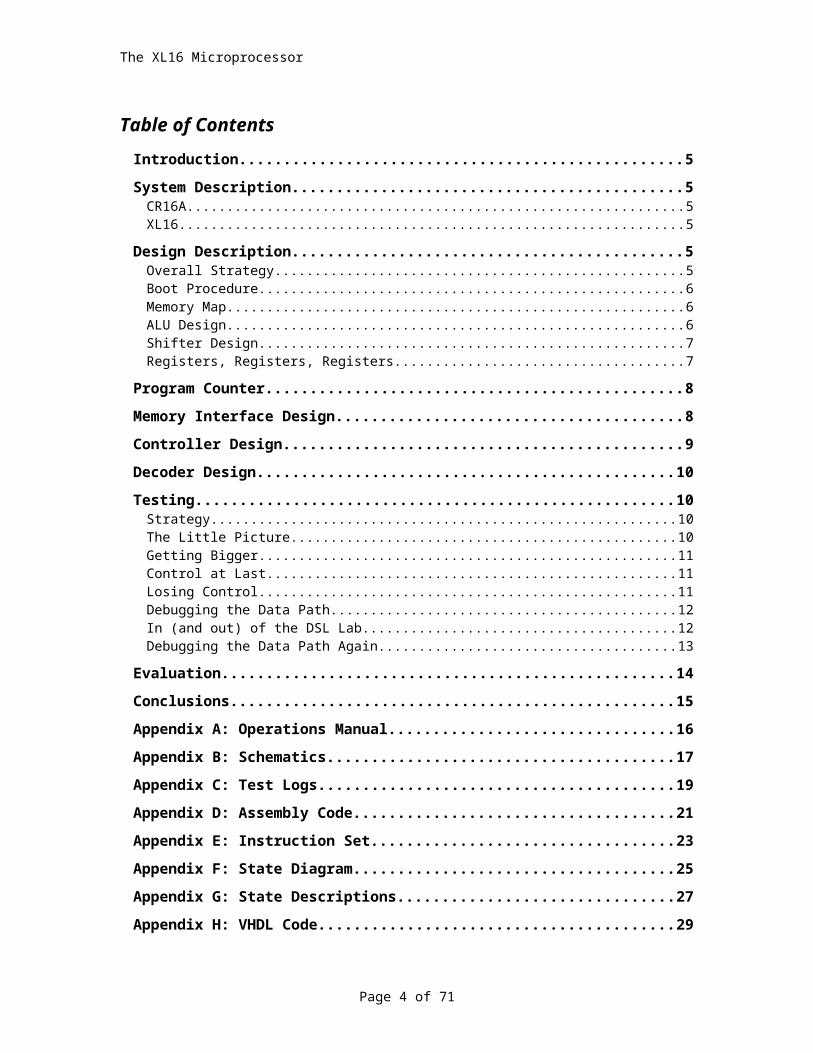
Table of ContentsIntroduction.................................................................................................................................5
System Description......................................................................................................................5CR16A......................................................................................................................................................5XL16.........................................................................................................................................................5
Design Description......................................................................................................................5Overall Strategy........................................................................................................................................5Boot Procedure.........................................................................................................................................6Memory Map............................................................................................................................................6ALU Design..............................................................................................................................................6Shifter Design...........................................................................................................................................7Registers, Registers, Registers.................................................................................................................7
Program Counter........................................................................................................................8
Memory Interface Design...........................................................................................................8
Controller Design........................................................................................................................9
Decoder Design..........................................................................................................................10
Testing........................................................................................................................................10Strategy...................................................................................................................................................10The Little Picture....................................................................................................................................10Getting Bigger........................................................................................................................................11Control at Last........................................................................................................................................11Losing Control........................................................................................................................................11Debugging the Data Path........................................................................................................................12In (and out) of the DSL Lab...................................................................................................................12Debugging the Data Path Again.............................................................................................................13
Evaluation..................................................................................................................................14
Conclusions................................................................................................................................15
Appendix A: Operations Manual............................................................................................16
Appendix B: Schematics...........................................................................................................17
Appendix C: Test Logs.............................................................................................................19
Appendix D: Assembly Code....................................................................................................21
Appendix E: Instruction Set.....................................................................................................23
Appendix F: State Diagram......................................................................................................25
Appendix G: State Descriptions...............................................................................................27
Appendix H: VHDL Code........................................................................................................29
Appendix I: Control Settings...................................................................................................45
Page 4 of 52

The XL16 Microprocessor
Page 5 of 52

The XL16 Microprocessor
IntroductionThe XL16 microprocessor was designed, developed, and tested between August 23, 2000 and December 8, 2000 for the class CS3710 at the University of Utah. During the course of the semester, each team of 2 – 3 students attempted to program their own microprocessor and communicate with an I/O device of their choice. This report details the experience and the design decisions of Mike Fivas and Piper Smith as they worked to complete this project.
System DescriptionCR16AThe XL16 microprocessor uses National Semiconductor Corporation’s CR16A microprocessor core for its programming model. The CR16A is a RISC architecture specifically designed for embedded systems. It supports an extended instruction set (for word or byte addressing), 16 general-purpose registers, and 18-bit address implementation, as well as exception handling and interrupts.
XL16The XL16 utilizes a sub-set of the CR16A’s instruction set and uses word addressing exclusively (see Appendix E.) The XL16 uses 16 bit addresses, so it does not utilize the far relative addressing available in the CR16A (we have found this to be quite suitable for the purposes of this class.) Our microprocessor includes an arithmetic logic unit, a shifter, a program counter, 16 general purpose registers, a process status register, a specialized memory interface which includes I/O control capability, and a state machine that controls the overall processing of the instructions.
Design DescriptionOverall StrategyOn the highest design level, the XL16 consists of a data path, an instruction decoder, and a main control. The data path contains the system components and the wires that connect them together. The data path is quite complex considering all of the possible paths that the data can follow. For example, the inputs to the adder may come from the general-purpose register, the immediate register, sign extended bits contained in the instruction, or a binary one which is added to one of the other inputs under certain conditions. The data path of the XL16 was designed, wired, and tested with the CAD tool Powerview.
The main control of the system consists of transitions to different states depending on which instruction is being executed. In each state, the main control: sets the outputs that select the appropriate values on the wires in the data path sets the appropriate clock enables for loading values into registers sends the appropriate read or write signals to memory makes sure that the memory state machine has finished all of its cycles before moving
ahead to the next stateThe microprocessor’s main state machine control behavior was programmed with VHDL, then simulated alone prior to being connected to the data path. Next it was tested directly
Page 6 of 52

The XL16 Microprocessor
in Powerview prior to being programmed onto a Xilinx chip. The main idea is that it is very convenient to design, implement, study, and view a data path that actually looks like a data path. We felt that it would be cumbersome and inconvenient to build a data path by writing VHDL code. (Not to mention the fact that if we had programmed the entire design in VHDL, it would not have fit onto the Xilinx chip.) On the other hand, by implementing the main control of the microprocessor with VHDL, we saved a lot of time and could easily view each state as well as read what each output was expected to be in any given state. We wanted to be sure and utilize as much of the Xilinx chip’s capabilities as possible without running out of space on the chip. In the end, we accomplished this lofty goal quite precisely by utilizing all 400 of the available CLBs on the Xilinx chip.
Boot ProcedureOne of the first design decisions was to start the machine running by utilizing an asynchronous clear signal. The reason for this was to make certain that all of the registers were initially loaded with 0’s at exactly the same time (and independent of the system’s clock.) This simplifies the boot up procedure and insures that the first instruction loaded is the one at address 0000/H.
Memory MapThe XL16 utilizes 64 KB of the 128KB of memory that are available with the CR16. As previously mentioned, the XL16 exclusively uses 16 bit word addressing. The lower 48KB of memory is available for code and data, while the upper 16 KB is for I/O only. Therefore addresses 0000/H – BFFF/H hold code and data, while addresses C0000/H – FFFF/H are reserved for I/O. The XL16 maps to LEDs for addresses C0XX/H and C1XX/H for the parallel port. The remainder of the I/O memory is available for future enhancements.
ALU DesignIn order to handle the basic addition and subtraction operations, we opted to use the ADSU16 adder from the Xilinx Library instead of creating our own adder from scratch. The ADSU16 is a 16-bit adder that adds, subtracts, and sends out overflow and carry signals – which was exactly what we needed. We decided to forgo the additional headache of actually building a component that was already easily accessible in favor of concentrating on other more complex areas of the data path design. We added some additional logic to utilize the ADSU16’s subtraction functionality in order to implement the compare instruction. Initially, we thought about using the comparator that already existed in the Xilinx library, but because of the simplicity of the logical implementation of the compare function and the fact that we were worried about space, we chose to build our own comparator. In order to implement the logical operations AND, OR, and XOR, we first created the logic needed to process the instruction for one bit of data and used two inputs in order to identify the desired operation. We created a symbol for it and put 16 of them together in order to implement the 16 bit logic operations. A mux signal was created to determine whether to choose the output from the adder/comparator or the logical operations.
Page 7 of 52

The XL16 Microprocessor
Shifter DesignOur shifter was designed to be independent of the basic add, subtract, compare, and logical operations. We thought it would simplify things and make the schematics neater to just keep it separate from the ALU operations. The shifter inputs were connected directly to the output mux but in shifted order. We used 4 X74-157 muxes from the Xilinx library and we controlled whether the data was shifted right or left via a mux. We could have used 16 one-bit muxes, but the 4 input muxes were chosen because they made the schematic easier to follow and work with. Little did we realize (at the time that the shifter was designed) how often we would utilize the shifting operation in the data path. The shifter was required to handle both right or left shifts as well as arithmetic or logical shifts. A signal is sent into the shifter that determines the direction of the shift. There is a signal that determines whether or not the shift is logical – for a logical shift, the high order bit is always 0. For an arithmetic shift, the sign bit always gets copied to the high order bit. In the data path, outside the shifter, there is mux that chooses whether the ALU/Logical output or the Shifter output is sent back to the general-purpose registers to be written.
Registers, Registers, RegistersIn order to implement the data path and to literally hold on to the various values, a variety of registers were needed.
We have 16 general-purpose registers that consist of two RAM16X8Ds from the Xilinx library. We choose to use these parts because we can read from two addresses simultaneously and we can write to one address at a time. We needed to use two in order to store the needed 16 bits of data, with half of the bits being stored in one register and the other 8 bits being stored in the other register. We then mapped both 8-bit words to the same address. The top port had the writing capability, so we designed the data path to always put the destination register address on the top port. This way we wouldn’t have to change it between the register read and the register write. The only other option as far as implementing the 16 registers was to build our own, but the RAM16X8D was perfectly suited to our needs and for all we knew, attempting to replicate it could be another semester long project.
Anytime we needed a register to hold 16 bits of data, we used the FD16CE – which is simply a 16 bit D flip flop. We didn’t really think we could save any space by putting together 16 single bit flip flops, so we went for the Xilinx library component that best suited our purposes. We used this type of a register for the Program Counter, Immediate Register, Instruction Register, and Memory Address Register. (Please note that the Memory Data Register will be discussed later in the “Memory Interface Design” section.)
The Processor Status Register consists of five FDCEs (single bit D flip flops.) Although the CR16 supports nine such registers, the XL16 only needs to utilize five of them: The “C” bit, which signifies a carry for an add or a borrow for a subtract instruction
Page 8 of 52

The XL16 Microprocessor
The “F” bit, which detects an overflow for an add or a subtract instruction The “N” bit, which detects a less-than comparison for signed integers The “L” bit, which detects a less-than comparison for unsigned integers The “Z” bit, which detects equality
Since the “C” and “F” bits are set separately from the “N”, “L”, and “Z” bits, we hooked the “C” and “F” clock enables together on one signal and then connected the remaining PSR clock enables together on another signal. This way we could update the correct register at the right time. It is also important to note that not every add or subtract operation updates the PSR.
Program CounterWe decided to use word addressing for the PC since all of our instructions and data are processed as words. In order to simplify the data path, we opted to utilize a separate adder for PC incrementing and branch displacements. We could have utilized the adder in the ALU, but we decided to implement the PC in this manner so that the PC logic was not intertwined with all of the other ALU operations. The adder used in the PC was a no frills ADD16 component, so it didn’t take up a significant amount of space.
Memory Interface DesignThe memory interface design consists of a state machine that controls the reads and writes for memory, a word address only memory control, and memory mapped I/O for memory, LEDs, and parallel ports. Since the memory is mapped the way it is, the clock-enable for the memory state machine is tied to the inverted I/O signal, so that if I/O is being accessed, the memory state machine does not run. The memory itself is accessed though the XSRAM, which was available in the cs3710 parts library to simplify the memory access for the purposes of this project.
The memory state machine was designed to control the bits that are read from and written to in the memory. The memory is byte addressed, and the XL16 uses word addresses and data, so a state machine was needed to control which part of the data was written to which memory address. Another twist is that the XSRAM may take several clock cycles to actually read or write the data. The initial design for the memory control state machine was to go through four states for each read, and four states for each write. The first state simply checks for a read or a write signal from the main control. Once a read or write signal is detected, the second state is entered. In the second state, the “memory is ready” signal is set to low, the low bit on the address line is set to low, and the lowest 8 bits of the data are sent to memory (for a memory write). In the third state we wait for the busy signal of the XSRAM to go low and when this happens, we enter the fourth state. In the fourth state, the low bit on the address line is set to high, and the highest 8 bits of data are sent to memory (for a memory write.) Once the XSRAM is done with its processing, the first state is again entered until the next read or write signal is detected. During testing, we discovered that our data was being overwritten on the memory writes, so we tweaked the state machine to go through all four states for each 8 bits when writing the data. The read was able to continue using the original four states in addition to a separate state
Page 9 of 52

The XL16 Microprocessor
machines that helps control the Memory Data Register. (See the “Testing” section for more details.)
Our Memory Data Register takes the bits that are sent out by the XSRAM and holds them until the next memory read. During a read the low 8 bits are stored and then the high 8 bits are stored so that all of the data can go out on the bus to the rest of the circuit in the correct word format. This enables the rest of the circuit to treat the memory as if it has 16 data bits, even though at its core it really has only eight.
The memory control for the I/O and LEDs was put in place in preparation for the I/O portion of the project. Unfortunately, this portion of the XL16 has not yet been tested on the hardware.
Controller DesignThe main control of the XL16 microprocessor is a state machine that is written in VHDL code. As mentioned earlier, much of the design of this microprocessor was implemented with schematics. Designing the data path in this manner was a great advantage in terms of readability and understanding. However, when it came to the controlling state machine for the system, it made more sense to design, code, analyze, and determine the overall behavior of the microprocessor by programming it in VHDL.
The main idea behind main control logic is that the VHDL control state machine receives signals from the control logic so that it can decipher exactly which instruction (or which variation of each instruction) is being executed.
Various mux signals, memory signals, and clock enables are set based on what data is needed, where the data needs to go and where the data should come from. This will vary for any particular instruction during any particular state. Some of the mux signals are set by logic within the circuit itself, but most of the signals are set by the main system control.
The main control starts running when the asynchronous clear signal of the microprocessor is set to high. Once the clear is then set to low, the state transitions begin. The first state initializes all outputs to the most common settings. The instruction is retrieved during the second state (the first instruction is required to be at address 0000/H.) Next the instruction is deciphered. This is done by examining the outputs of the instruction decoder. The instruction is then identified as being a basic ALU operation, a shift operation, a move operation, a load or store operation, a conditional jump or branch operation, a jump and link, a branch and link operation, or a “no-op” operation. For a detail of each state and what happens in each state, see appendices F, G, and H. The basic idea is that the instruction decoder signals include information regarding whether or not the instruction deals with a large immediate coming from the next word in memory, a small immediate coming from certain bits contained in the instruction itself, or a value coming from the general-purpose register. The state machine then takes this information and progresses through the applicable states, which set the various control signals so that the right data values are transferred along the data path. The decoder signals could have
Page 10 of 52

The XL16 Microprocessor
been wired to connect directly to the control settings in the circuit, but since we categorized these as behavioral issues, we decided to simply implement them directly in VHDL.
Decoder DesignEach instruction is decoded based on the bits contained in the first word of the instruction. The signals are then set and passed into the main system control so that the instruction is processed correctly. Each instruction is decoded with gate logic right in the circuit. This could have been implemented directly in the VHDL main control logic by sending in the instruction word and doing the decoding in there. We decided to implement the decoding in a separate circuit because it was faster and just as easy to analyze and work with. We also thought that implementing it in this manner may save on space, since by this time we were becoming more concerned with that aspect of the microprocessor! We also discovered that having these signals outside of the VHDL code made it much easier to test and find problems with the circuit.
TestingStrategyThe strategy for testing the XL16 was “bottom up” in design. Our plan was to test each piece independently, then to hook up the data path and then test each instruction at that level prior to implementing the main control. Next we would test the main control alone. Finally, we would hook the main control up to the rest of the data path and test it with the main control symbol as a “module”, so that we could actually watch the current state as we tested the circuit.
Once we got the circuit simulating correctly, we would change the symbol for the main control to “composite” (where the VHDL code is actually translated into circuits) and, theoretically, it should still simulate perfectly. Once that was verified, we could program our design on the Xilinx chip, and again theoretically, it would work as expected right on the chip.
The Little PictureIn the beginning stages of the project, the testing was not extremely complex. We were able to test each piece of the microprocessor separately by simulating with the Powerview tool. By testing each part on an individual basis, we were able to catch bugs that would have been more difficult and time consuming to find in a larger circuit. We were able to correct many logical errors during this process. We were also able to test out various parts from the Xilinx library and become familiar with how they worked and whether or not we could utilize them in the project. (Test logs are in Appendix C.)
When we tested each component, we used command files with “check” statements. As we debugged, we found that sometimes there was something wrong with the component we were testing, and sometimes there was an error in the “check” statement. Once any given module passed our tests, we were sure that it was good to go, because we tried each operation that need to be processed. For example, when we tested the bit logic, we tested
Page 11 of 52

The XL16 Microprocessor
for AND, OR and XOR operations. When we tested the adder, we tried both add and subtract. On the shifter, we tried a right shift and a left shift for both the arithmetic and the logical shift. For the PC, we tested capability for incrementing, displacements, and jumps. For the memory and general-purpose registers we tested both reads and writes.
Getting BiggerOnce we hooked everything up and created our data path, we realized that simulating would be a nightmare. Even though we had initially planned to test the data path before adding the main control, we felt that it would be better to spend our time implementing the main control rather than attempting to step through each instruction without it.
Control at LastNext we designed and implemented the main controlling state machine in VHDL code. After fixing various syntax errors and correctly designating our input and output signals, we finally got the code to compile. We also successfully got the code to simulate in Powerview (still not connected to the rest of the circuit yet) and it worked perfectly! We were really set.
Next it was time to hook the VHDL code up to the rest of the circuit. We worked for a long time at trying out the optional testing option where the VHDL logic is put into a symbol without creating the wire file. We really wanted to test in this manner because we knew the easiest way to debug would be to be able see which state we were in as the assembly code executed. After banging our heads against the wall for awhile, (unable to resolve one error) we decided to attempt to create the wire file. We followed the instructions step by step, and at last we had a symbol with wires behind it! But now we continued to be plagued by strange errors connected with the new symbol. Finally those errors were resolved when we removed the attributes in the symbol that had been set earlier when the VHDL symbol processing was done. We were finally ready to simulate our entire data path.
Losing ControlWe had the example assembly program, we had the main control, we had the decoder, and we had the data path. Nothing could stop us now. Except that nothing was working right. We couldn’t make sense out of the states, and although all of the signals reset to zero properly, everything kept going to X’s. Oh yeah! We needed to set the Read and Write signals low in the XSRAM symbol. So we did that, and then……. the states still did not make sense and the outputs from the main control did not consistently appear as cute little 0’s and 1’s. We were plagued with X’s. We couldn’t figure out what in the world was going on. We already knew that the main control simulated correctly by itself. There was one possibility. The VHDL code was written in a different style than the example that had been provided in class. The code simulated fine by itself, and there appeared to be no logical reason why rewriting it would improve the situation. With no other explanations in sight, we rewrote 11 pages of VHDL code.
After rewriting all that code, we worked at recreating the wire file. We got clear to the ViewGen process and we were stuck again. We tried it again after deleting the
Page 12 of 52

The XL16 Microprocessor
previously created wire files and found success at last! The main control output signals were working and state transitions were taking place! Our success was short-lived, however, when the dreaded X’s appeared on the bits coming out of our instruction register. But at least we were…
Debugging the Data PathWe started out by testing the example.s assembly program that was provided for the class. We crashed somewhere on every instruction that we attempted to execute. We discovered that one problem was with the new VHDL code. In the original code we allowed signals to carry through from state to state without being explicitly set each time. In the new code each signal had to be set on each state, and we missed a few. Then one by one we fixed problems until we could successfully (or so we thought) run example.s. Here is a list of the problems that we encountered along with their resolutions:Symptom Problem ResolutionX’s coming from the instruction register
The addresses were being set backwards so the instructions were not being found.
Switch around the control signals in the memory data register
X’s coming from the instruction register
The wrong value was going into….
Use the right mux control setting
X’s coming from the instruction register
The memory read signal was staying high too long
Only set the memory read signal for one state
X’s coming from the instruction register
Sending byte addresses (instead of words) into the memory when executing loads
Convert the addresses to words for the appropriate instructions
X’s coming from the instruction register
Selecting the wrong values for various operations
Use the right mux control settings
This Use the right mux control settings
And that Use the right mux control settings
And the other Use the right mux control settings
And some more Use the right mux control settings
In (and out) of the DSL LabNow that we could get through example.s (and many instructions from an assembly code program that we had written), we decided to program our creation onto the Xilinx chip and try it out. We tried it out by running it on the hardware and we had no luck. We did, however, get a hold of two more assembly programs that ran quite extensive tests. These tests were more extensive than any assembly code that we had written, so we thought that we should discontinue writing our own assembly code until we could at least get through the complex programs that were available for class use. It was the bottom of the ninth, it
Page 13 of 52

The XL16 Microprocessor
was day 28 of election 2000, there were two days to go until the project deadline, and we were…..
Debugging the Data Path AgainStep by step we debugged our data path. We discovered things that we had never thought of before. We not only discovered problems with each instruction, but we encountered problems with each variation of each instruction. Here is a list of the fixes that we had to make in order to get the test0000.s program to run.Problem FixThe wrong address was being read for store instructions
The “Add-Select” on the adder needed to be set for load and store operations. This was a difficult one to find as we found that the add usually works without “Add-Select” being set, so sometimes load and store works sometimes it doesn’t.
Values in the memory were being overwritten incorrectly
When executing a memory write, go though the entire memory state machine cycle for each 8 bits that are written. We did not have time to redesign the memory state machine, and we knew that other groups were having to put in extra states to get the microprocessor to work on the hardware, so we thought this would be a good resolution.
Getting an off by one error on a SUBC instruction
We were incorrectly setting the microprocessor status register’s “C” bit on subtraction instructions. We had been setting it as if it were a carry from an add, instead of a borrow from a subtract.
Branching to the wrong place The sign extender needed to be altered and the low bit of the branch displacement had to be ignored so that it would match up to our 16 bit word addressed program counter value. We also discovered that we actually needed the 16th bit (from the first word) of the displacement of the Branch and Link instruction since we had to throw out the low bit.
Now that we could successfully run test0000.s, we found that we could also successfully run test1234.s. With 3 hours to go until the project deadline, we worked on converting our design into hardware once again. We were hoping that everything would fit on the chip. We knew it would be close. If the design did not fit, then we would have to try it with a different XSRAM chip that would lengthen and complicate our hardware testing process. In the end we successfully downloaded our program onto the Xilinx chip using all 400 of the CLB’s that were available. This was strange, because when we only needed 397 CLB’s it wouldn’t fit. We ran test0000.bin on the hardware, checked the
Page 14 of 52

The XL16 Microprocessor
memory, and found all of the correct values at the correct addresses! We were very happy to be one of the five teams who were able to successfully implement their microprocessor on the hardware by the project deadline.
EvaluationSince the XL16 microprocessor did end up functioning properly on the hardware, it certainly must have had an acceptable design! Also even though we ended up having to fix a lot of things during the final testing, we did not have to totally redesign anything, which shows that we were not too far off from the target as the semester progressed. We also only wrote to hardware twice, which would have saved a lot of money if we were still in the age of write once chips. All of the individual components functioned well, the decoder properly identified instructions, and the main control interpreted the input signals correctly to produce the proper output signals. But if we’d have known at the beginning of the semester what we know now…
Writing so much of the control logic into the VHDL instead of directly in the circuit ended up being a mixed blessing. When we were debugging, (after we finally got the VHDL code to work) it was nice to be able to go into the VHDL file and just add a line of code here and there (or comment out a line or two) in order to fix problems. The disadvantage was that it was a time consuming process to run Synopsis and get the new code ready to simulate in the circuit again. On top of that, Synopsis would not always work (depending on which computer you happened to be logged into.) Using VHDL for so much of the behavioral logic would have been great if we would have been able to simulate it while watching the actual current state information. Luckily we separated our control logic from the VHDL, which helped us to keep track of the states. Without that advantage, we probably would have been better off setting the signals directly by using the decoded instruction information. If we would have done it that way, we also might have used less space on the Xilinx chip. In any case, we could have also cut down the number of states, if time would have permitted.
If we could do it again, we would have tested each component with more of the big picture in mind, but it was hard to see the big picture early on. For example, when we tested the ALU, we just tried adding and subtracting – this is when we should have investigated the ADDC and SUBC instructions. Then we could have tested for the capability of executing those instructions as well. As it was, we ended up implementing the ADDC and SUBC instructions after we had initially designed our data path. When we incorporated bottom up testing, we should have done it with more of a top down frame of mind. We should have tried to implement each instruction to the appropriate module way back when we first started testing. If we would have done that, then maybe we could have implemented some impressive I/O during the last week instead of debugging and fixing the branch displacement logic.
ConclusionsThe project was very difficult to complete in the time permitted, but fun to work on. This would be a great class to take when you don’t have anything else going on in your life. On the plus side, we learned a lot. We used to think that the sender/receiver assignment
Page 15 of 52

The XL16 Microprocessor
from cs3700 incorporated a lot of logic, wires, and symbols. The semester may have worked a little smoother if the early labs were given less time to leave more time at the end of the semester for debugging the whole machine. We don’t think that anything this semester was busy work, because we used it all to complete the project. Even the little state machine that we built at the beginning of the semester was helpful to get back into the digital logic and see that the Xilinx part would really work.
On the negative end, the Powerview and Synthesis tools would sometimes freak out for no reason. It was also nearly impossible to share files, so we ended up working together from one account a lot. We usually needed two minds when working on this project, so it worked out fine. It was also a drag that we couldn’t get the circuit to simulate with the VHDL code so that we could easily see the current state.
Page 16 of 52

The XL16 Microprocessor
Appendix A: Operations Manual1. Load the memory so that the first instruction is located at address 0000/H (see xcess
instruction manual)2. Set the clear signal high3. Set the clear to low4. The machine is now executing instructions
Page 17 of 52

The XL16 Microprocessor
Appendix B: Schematics
Page 18 of 52

The XL16 Microprocessor
Page 19 of 52

The XL16 Microprocessor
Appendix C: Test Logs
Page 20 of 52

The XL16 Microprocessor
Page 21 of 52

The XL16 Microprocessor
Appendix D: Assembly Code
Page 22 of 52

The XL16 Microprocessor
Page 23 of 52

The XL16 Microprocessor
Appendix E: Instruction Set
Page 24 of 52

The XL16 Microprocessor
Page 25 of 52

The XL16 Microprocessor
Appendix F: State Diagram
Page 26 of 52
The XL16 Microprocessor
Page 27 of 52

The XL16 Microprocessor
Appendix G: State DescriptionsState DescriptionsState DescriptionStart Determines when to startLdinst Loads the instruction into memoryDecipher Sends the instruction to the correct path of
executionAlu Sets up the addresses going into the GPR and
determines whether the alu instruction deals with a value from the register, a small immediate in the current instruction, or a big immediate in the next instruction
Aluc Adds or subtracts 1 from/ to the R-dest valueAluc2 Adds or subtracts the source value from the value
that just came out of the alu Alureg Alu operation where the source is coming from the
GPRAlusmall Alu operation with source coming from an
immediate in the current wordAlubig Alu operation with source coming from an
immediate in the next word – increments the pcLdimm Loads the value coming from memory into the
immediate registerAluselb Set up the data goin into the bottom alu input to
come from the immediate registerAlusto Load the data coming out of the alu into the GPRIncpc2 Increment the pcShift Set the proper addresses; sets up muxes so the data
that goes back into R-dest comes from the shifterMove Sets up the addresses going into the GPR and
determines whether the alu instruction deals with a value from the register, a small immediate in the current instruction, or a big immediate in the next instruction
Movereg Move the item from a register to another registerMovesmall Move the item from an immediate in the instructionMovebig Move the item from an immediate in the next word.
Increment the pcLdmov Read the word from memory for a movebig
operationLdsto Determines whether to load from a large or small
offsetLdstosmall Takes the value coming out of the alu (from a small
offset) and loads it into the MARLdread Reads the address coming from the MARPostLdread Give the memory an extra state to readLdgpr Loads the value coming from memory into the GPRLdstobig Increment the pcImmldsto Load the immediate registerLdaddimm Set up to add gprB and the value from the
immediate registerLdabsimm Determine whether to do a load or a store operation
Page 28 of 52

The XL16 Microprocessor
Stoset Set up muxes for a write to memoryStowrite Write to memoryPostStoWrite Give the memory an extra state to writeCond Determine whether or not the condition is true and
if it is, then determine whether it is a branch or a jump
Br Determine whether the branch displacement is coming from a small or a big immediate
Jlink Store the next value from the pc into the link register (without actually updating the pc)
Jump Load the pc with the value coming from the target register
Brgetimm Update the pc to get the next wordLdimmbr Read the memory, load the immediate register, and
determine whether or not this is a branch and link instruction
Brimm Add the sign extended branch displacement to the current pc
Brlink Store the next pc into the link register (without actually updating the pc)
Brbigimm Add the immediate from the immediate register to the current pc
Page 29 of 52

The XL16 Microprocessor
Appendix H: VHDL Code--Mike Fivas & Piper Smith--12/02/00--Lab 6--State Machine Controller--This controls the many mux settings in the datapath as the instructions--are executed
---------------------------------------------------------------------1. Packages-------------------------------------------------------------------library IEEE;use IEEE.std_logic_1164.all;
library SYNOPSYS;use SYNOPSYS.attributes.all;
entity xlsim2 is port (CLK: in STD_LOGIC;
clear: in STD_LOGIC; pc_update: out STD_LOGIC;
pcadd_select: out STD_LOGIC;pc_select: out STD_LOGIC;pcimm_sel: out STD_LOGIC;imm_sel: out STD_LOGIC;imm_ce: out STD_LOGIC;gpr_sel: out STD_LOGIC;gpr_ce: out STD_LOGIC;gprd_sel0: out STD_LOGIC;gprd_sel1: out STD_LOGIC;gprb_se_sel: out STD_LOGIC;alu_gprb_sel0: out STD_LOGIC;alu_gprb_sel1: out STD_LOGIC;--alu_select: in STD_LOGIC;alu_data_sel: out STD_LOGIC;--sh_data_sel: out STD_LOGIC;sub_select: in STD_LOGIC;add_select: in STD_LOGIC;addc_sel: out STD_LOGIC;
c_sel: out STD_LOGIC;addu: in STD_LOGIC;cmp: in STD_LOGIC;cf_clken: out STD_LOGIC;nlz_clken:out STD_LOGIC;ls_abs: in STD_LOGIC;
Page 30 of 52

The XL16 Microprocessor
mar_sel: out STD_LOGIC;mar_ce: out STD_LOGIC;ir_ce: out STD_LOGIC;mem_data_sel: out STD_LOGIC;mem_sel: out STD_LOGIC;memread: out STD_LOGIC;memwrite: out STD_LOGIC;answer_sel: out STD_LOGIC;cout: in STD_LOGIC;--fout: in STD_LOGIC;--nout: in STD_LOGIC;--lout: in STD_LOGIC;--zout: in STD_LOGIC;--pc_d0: out STD_LOGIC;--pc_d1: out STD_LOGIC;--pc_d2: out STD_LOGIC;--pc_d3: out STD_LOGIC;memready: in STD_LOGIC;reg: in STD_LOGIC;bigimm: in STD_LOGIC;ldstobig: in STD_LOGIC;
ld_op: in STD_LOGIC;jump: in STD_LOGIC;link: in STD_LOGIC;branch: in STD_LOGIC;cond: in STD_LOGIC;condeval: in STD_LOGIC;brbig: in STD_LOGIC;nop: in STD_LOGIC;alu_op: in STD_LOGIC;shift_op: in STD_LOGIC;move_op: in STD_LOGIC;ldsto_op: in STD_LOGIC;
c: in STD_LOGIC);end xlsim2;
architecture xlsim2_arch of xlsim2 is-- Symbolic encoded state machine: Sreg0type states is (start,ldinst,decipher,alu,alureg,alusmall,alubig,ldimm,
aluselb,alusto,incpc2,aluc,aluc2,shift,move,movreg,movsmall,movbig,ldmov, movsto,ldsto,ldstosmall,ldread,ldgpr,ldstobigst,immldsto,ldaddimm,ldabsimm,stoset,stowrite,poststowrite,postldread,
jumpst,condst,br,ldimmbr,brimm,jlink,brlink,brgetimm,brbigimm);signal current_state:states;
Page 31 of 52

The XL16 Microprocessor
--This process takes care of the combinational logic portion of the state machinebegin
state_machine: process (CLK,clear)begin-- this process uses an asynchronous clear
if clear='1' thencurrent_state <= start;
else if CLK'event and CLK = '1' then case current_state is
when start =>
current_state <= ldinst;
when ldinst =>
if (memready='1') thencurrent_state <= decipher;
elsecurrent_state <= ldinst;
end if;
when decipher =>
if (nop='1') then-- just go to the next instructioncurrent_state <= incpc2;
elsif (alu_op='1') then-- alu instructioncurrent_state <= alu;
elsif (shift_op='1') then-- shift instructioncurrent_state <= shift;
elsif (move_op='1') then-- move instructioncurrent_state <= move;
elsif (ldsto_op='1') then-- load or store instructioncurrent_state <= ldsto;
elsif (cond='1') then-- Jcond or Bcond instructioncurrent_state <= condst;
elsif (jump='1' AND link='1' and cond='0') then-- JAL instruction
Page 32 of 52

The XL16 Microprocessor
current_state <= jlink;elsif (branch='1' and cond='0') then
-- BR instructioncurrent_state <= br;
elsif (jump='1' and link = '0' and cond='0') then-- Jump instructioncurrent_state <= jumpst;
end if;--------------------------------------------------------------------------
when alu =>-- sets the register address inputs and-- determines how to process the alu instruction
if (reg='1' AND (cout='0' or c = '0')) then-- alu instruction where value is coming from a -- register
current_state <= alureg;end if;if (bigimm='1' AND (cout='0' or c = '0')) then-- alu instruction where value is coming from an -- immediate in the next instruction
current_state <= alubig;end if;if (bigimm='0' AND reg = '0' and (c = '0' or cout='0')) then-- alu instruction where value is coming from an -- immediate in the current instruction
current_state <= alusmall;end if;if (c='1' AND cout='1') then-- SUBC or ADDC instruction where the PSR.C = 1
current_state <= aluc;end if;
when aluc =>
current_state <= aluc2;
when aluc2 =>
if (reg='1') then-- alu instruction where value is coming from a -- register
current_state <= alureg;end if;if (bigimm='1') then
Page 33 of 52

The XL16 Microprocessor
-- alu instruction where value is coming from an -- immediate in the next instruction
current_state <= alubig;end if;if (bigimm='0' AND reg = '0') then-- alu instruction where value is coming from an -- immediate in the current instruction
current_state <= alusmall;end if;
when alureg =>-- alu operation with source coming from -- a register--alu_data_sel <= '1';current_state <= alusto;
when alusmall =>-- alu operation with source coming from -- an immediate in the instruction--alu_data_sel <= '0';--imm_sel <= '1';current_state <= alusto;
when alubig =>-- alu operation with source coming from -- an immediate in the next word-- increment the pc
current_state <= ldimm;
when ldimm =>-- load the value coming from memory into-- the immediate register
if (memready = '1') thencurrent_state <= aluselb;
elsecurrent_state <= ldimm;
end if;
when aluselb =>-- set up the data going into the bottom-- alu input to come from the immediate register
current_state <= alusto;
Page 34 of 52

The XL16 Microprocessor
when alusto =>-- load the data coming out of the alu-- into the GPR
current_state <= incpc2;
-- discontinue loading the PSR register--cf_clken <= '0';--nlz_clken <= '0';
when incpc2 =>-- increment the pc
current_state <= ldinst;
when shift => -- the data that goes back into R-Dest-- should come from the shifter
current_state <= alusto;
when move => if (reg='1') then-- move where value is coming from a -- register
current_state <= movreg;end if;if (bigimm='1') then-- move where value is coming from an -- immediate in the next instruction
current_state <= movbig;end if;if (bigimm='0' AND reg = '0') then-- move where value is coming from an -- immediate in the current instruction
current_state <= movsmall;end if;
when movreg => -- move the item from a register to another-- register
current_state <= alusto;
when movsmall => -- move the item from an immediate
Page 35 of 52

The XL16 Microprocessor
-- in the instruction
current_state <= alusto;
when movbig => -- move the item from an immediate-- in the next word-- increment the pc
current_state <= ldmov;
when ldmov => -- read the word from memory
if (memready = '1') thencurrent_state <= alusto;
elsecurrent_state <= ldmov;
end if;
when ldsto => -- determine what to do with-- the load or store operationif (ldstobig = '1') then
current_state <= ldstobigst;else
current_state <= ldstosmall;end if;
when ldstosmall =>
if (ld_op = '1') thencurrent_state <= ldread;
elsecurrent_state <= stoset;
end if;
when ldread =>--mar_ce <= '0';--memread <= '1';
current_state <= postldread;
when postldread => --memread <= '0'; if (memready = '1') then
Page 36 of 52

The XL16 Microprocessor
current_state <= ldgpr; else current_state <= postldread; end if;
when ldgpr =>
current_state <= incpc2;
when ldstobigst =>-- increment the PC
current_state <= immldsto;
when immldsto =>-- load the immediate register--pc_update <= '0';--imm_ce <= '1';--memread <= '1';if (memready = '1' AND ls_abs = '0') then
current_state <= ldaddimm;elsif (memready = '1' AND ls_abs = '1') then
current_state <= ldabsimm;elsif (memready = '0') then
current_state <= immldsto;end if;
when ldaddimm =>-- add gprb + imm
if (ld_op = '1') thencurrent_state <= ldread;
elsecurrent_state <= stoset;
end if;
when ldabsimm =>-- load the immediate register
if (ld_op = '1') then --memread <= '1';
current_state <= ldread;else
current_state <= stoset;end if;
Page 37 of 52

The XL16 Microprocessor
when stoset =>-- get ready to write to memory
current_state <= stowrite;
when stowrite =>-- write to memory--memwrite <= '1';if (memready = '1') then-- current_state <= incpc2;
current_state <= poststowrite;else
current_state <= stowrite;end if;
when poststowrite => if (memready = '1') then current_state <= incpc2; else current_state <= poststowrite; end if;
when condst =>-- determine if condition is true-- if so, take either br or jumpif (condeval = '1') then
if (branch = '1') thencurrent_state <= br;
elsecurrent_state <= jumpst;
end if;else
current_state <= incpc2;end if;
when br =>-- determine small or med immediateif (brbig = '0') then
current_state <= brimm;else
current_state <= brgetimm;end if;
when jlink =>
Page 38 of 52

The XL16 Microprocessor
-- do not change the PC value!-- just get the next one for storage purposes
current_state <= jumpst;
when jumpst =>-- jump to the address coming from R-Target
current_state <= ldinst;
when brgetimm =>-- get the next word
current_state <= ldimmbr;
when ldimmbr =>
if (memready = '1') thenif (link = '1') then
current_state <= brlink;else
current_state <= brbigimm;end if;
elsecurrent_state <= ldimmbr;
end if;
when brimm =>-- add the sign extended branch value to the current PC
current_state <= ldinst;
when brlink =>-- do not change the PC value!-- just get the next one for storage purposes
current_state <= brbigimm;
when brbigimm =>-- add the immediate from reg to the current PC
current_state <= ldinst;when others =>
null;end case;end if;
Page 39 of 52

The XL16 Microprocessor
end if;end process;
--This process sets the current statue of the state machine--on the clock event, with an asynchronous clear--sttrans: process (CLK,clear)--begin-- if clear='1' then
-- current_state <= start;-- elsif (CLK = '1' and CLK'event) then
-- current_state <= next_state;-- end if;--end process;
--signal assignment -- set all signals to zero pc_update_assignment: pc_update <= '1' when (current_state = alubig) else '1' when (current_state = incpc2) else '1' when (current_state = movbig) else '1' when (current_state = ldstobigst) else '1' when (current_state = jumpst) else --'1' when (current_state = brgetimm) else '1' when (current_state = brimm) else '1' when (current_state = brbigimm) else '0';
pcadd_select_assignment: pcadd_select <= -- changed Sunday (all parts) -- '1' when (current_state = start) else -- '1' when (current_state = ldinst) else -- '1' when (current_state = alubig) else -- '1' when (current_state = incpc2) else -- '1' when (current_state = movbig) else -- '1' when (current_state = ldstobigst) else -- '1' when (current_state = jlink) else -- '1' when (current_state = brgetimm) else -- '1' when (current_state = brimm) else -- '1' when (current_state = brlink) else -- '1' when (current_state = brbigimm) else '0' when (current_state = brimm) else '0' when (current_state = brbigimm) else '1';
pc_select_assignment: pc_select <= '1' when (current_state = start) else '1' when (current_state = ldinst) else
Page 40 of 52

The XL16 Microprocessor
'1' when (current_state = alubig) else '1' when (current_state = incpc2) else '1' when (current_state = movbig) else '1' when (current_state = ldstobigst) else '1' when (current_state = jlink) else '1' when (current_state = brgetimm) else '1' when (current_state = brimm) else '1' when (current_state = brlink) else '1' when (current_state = brbigimm) else '0';
pcimm_sel_assignment: pcimm_sel <= '1' when (current_state = brimm) else '0'; imm_sel_assignment: imm_sel <= '1' when (current_state = brimm) else '1' when (current_state = alusto and bigimm = '0') else '1' when (current_state = alusmall) else '1' when (current_state = ldstosmall) else '0'; imm_ce_assignment:
imm_ce <= '1' when (current_state = ldimm) else '1' when (current_state = immldsto) else '1' when (current_state = ldimmbr) else '0'; gpr_sel_assignment:
gpr_sel <= '1' when (current_state = jlink) else '1' when (current_state = brlink) else '0'; gpr_ce_assignment:
gpr_ce <= '1' when (current_state = alusto) else '1' when (current_state = ldgpr) else '1' when (current_state = jlink) else '1' when (current_state = brlink) else '0'; gprd_sel0_assignment:
gprd_sel0 <= '1' when (current_state = ldmov) else '1' when (current_state = ldgpr) else
--added Sunday
Page 41 of 52

The XL16 Microprocessor
'1' when (current_state = alusto and move_op = '1' and bigimm = '1') else '0'; gprd_sel1_assignment:
gprd_sel1 <= -- removed Sunday '1' when (current_state = alu) else -- removed Sunday '1' when (current_state = shift) else -- removed sunday '1' when (current_state = ldmov) else '1' when (current_state = ldgpr) else
--added Sunday '1' when (current_state = alusto and move_op = '1' and bigimm = '1') else '1' when (current_state = alusto and alu_op = '1') else '1' when (current_state = alusto and shift_op = '1') else '0'; gprb_se_sel_assignment:
gprb_se_sel <= '1' when (current_state = movsmall) else
--added Sunday '1' when (current_state = alusto and reg = '0' and bigimm = '0') else '1' when (current_state = alusto and alu_op = '1') else '0'; alu_gprb_sel0_assignment:
alu_gprb_sel0 <= '1' when (current_state = ldstosmall) else '0'; alu_gprb_sel1_assignment:
alu_gprb_sel1 <= '1' when (current_state = alu) else -- '1' when (current_state = ldstosmall) else '1' when (current_state = aluc) else '1' when (current_state = aluc2) else '1' when (current_state = alusmall) else '1' when (current_state = alusto and bigimm = '0' and reg = '0') else '1' when (current_state = alusto and alu_op = '1') else '0';
--alu_select <= '0'; alu_data_sel_assignment:
alu_data_sel <= '1' when (current_state = aluc) else '1' when (current_state = aluc2) else '1' when (current_state = alureg) else
Page 42 of 52

The XL16 Microprocessor
'1' when (current_state = ldstosmall) else '1' when (current_state = ldaddimm) else '1' when (current_state = alusto and reg = '1') else '0';
--sh_data_sel <= '0';--sub_select <= '0';--add_select <= '0';
addc_sel_assignment: addc_sel <= '1' when (current_state = aluc) else
'0'; c_sel_assignment: c_sel <= '1' when (current_state = aluc2) else '1' when (current_state = alusmall and c = '1' and cout = '1') else '1' when (current_state = alusto and c = '1' and cout = '1') else '1' when (current_state = aluselb and c = '1' and cout = '1') else '1' when (current_state = alureg and c = '1' and cout = '1') else '0'; cf_clken_assignment:
cf_clken <= '1' when (current_state = alusto and add_select = '1' AND addu = '0') else '1' when (current_state = alusto and sub_select = '1' AND cmp = '0') else '0'; nlz_clken_assignment:
nlz_clken <= '1' when (current_state = alusto and cmp = '1') else '0';
--mar_sel <= '0'; mar_ce_assignment:
mar_ce <= '1' when (current_state = alubig) else --'1' when (current_state = ldimm) else '1' when (current_state = incpc2) else '1' when (current_state = movbig) else '1' when (current_state = ldstosmall) else '1' when (current_state = ldstobigst) else '1' when (current_state = ldaddimm) else -- removed Sunday '1' when (current_state = ldimmbr) else
--added Sunday
Page 43 of 52

The XL16 Microprocessor
'1' when (current_state = jumpst) else '1' when (current_state = brimm) else '1' when (current_state = brbigimm) else '1' when (current_state = brgetimm) else '0'; mem_data_sel_assignment:
mem_data_sel <= '1' when (current_state = stoset) else '1' when (current_state = stowrite) else --added 12/7 '1' when (current_state = poststowrite) else '0'; mem_sel_assignment:
mem_sel <= -- removed Sunday '1' when (current_state = ldabsimm) else
--added Sunday '1' when (current_state = ldread and ls_abs = '1') else '1' when (current_state = postldread and ls_abs = '1') else '1' when (current_state = stoset and ls_abs = '1') else '1' when (current_state = stowrite and ls_abs = '1') else '1' when (current_state = poststowrite and ls_abs = '1') else '0'; memwrite_assignment:
memwrite <= '1' when (current_state = stoset) else '1' when (current_state = stowrite) else '0'; answer_sel_assignment:
answer_sel <= '1' when (current_state = alu) else '1' when (current_state = aluc) else '1' when (current_state = aluc2) else '1' when (current_state = alubig) else '1' when (current_state = alusmall) else '1' when (current_state = alureg) else '1' when (current_state = ldimm) else '1' when (current_state = aluselb) else '1' when (current_state = alusto and alu_op = '1') else '0'; ir_ce_assignment:
ir_ce <= '1' when (current_state = ldinst) else '0';
Page 44 of 52

The XL16 Microprocessor
-- prepare for memory read mar_sel_assignment:
mar_sel <= --removed Sunday '0' when (current_state = ldstobigst ) else '0' when (current_state = ldstosmall ) else '0' when (current_state = ldabsimm) else '0' when (current_state = ldaddimm) else '1'; memread_assignment:
memread <= '1' when (current_state = start) else '1' when (current_state = alubig) else '1' when (current_state = incpc2) else '1' when (current_state = movbig) else '1' when (current_state = ldread) else '1' when (current_state = ldstobigst) else --removed Sunday '1' when (current_state = immldsto) else '1' when (current_state = brgetimm) else --'1' when (current_state = ldinst) else --'1' when (current_state = ldimm) else --'1' when (current_state = ldmov) else --'1' when (current_state = postldread) else --'1' when (current_state = immldsto) else --'1' when (current_state = ldimmbr) else
--added Sunday '1' when (current_state = jumpst) else '1' when (current_state = brimm) else '1' when (current_state = brbigimm) else '0';end xlsim2_arch;
Page 45 of 52

The XL16 Microprocessor
Appendix I: Control SettingsLab 5: Input/Output ChartSchematic Reference I/O Name Description Input DataGeneral Clk The top-level clock
signal for the circuit.Clear The top-level clear
signal for the circuit.
ALU Sub-Comp Selection for executing subtraction or compare. This is actually the Carry In bit on the adder.
1: Subtract or Compare0: Addition
Add-Sel Selection for executing addition. This is actually the Add-Select input on the adder.
1: Addition0: Subtraction
ALU-Select Select between the value from the Add/Subtract/Compare function OR the 16 bit logic function.
1: Bit Logic0: Add/Sub/Comp
IMM-Sel Select between the (possibly sign extended) immediate from the instruction and the value from the Immediate Register.
1: Use the value from the instruction register.0: Use the value from the immediate register.
ALU-Data-Sel Selects the value that goes into the ALU’s port B.
1: Use the value from the General Purpose Register port B (R-Source)
0: Use the value from the ALU’s IMM-Sel. Selects between the (possibly sign extended) immediate from the instruction and the value from the Immediate Register.
Log-S1 Bit to select the logic function to perform.
Operation S1 S0AND 1 0OR 1 1XOR 0 1
Log-S0 Bit to select the logic function to perform.
Operation S1 S0AND 1 0OR 1 1XOR 0 1
A[15:0] Input 1 to the ALU
Page 46 of 52

The XL16 Microprocessor
B[15:0] Input 2 to the ALU
Overflow Set by addition/subtraction – not by compare
Sets PSR.F accordingly
Carry Carry Out. Set by addition/subtraction – not by compare
Sets PSR.C accordingly
PSR-Z Zero bit: Set by Subtraction – not by compare
0: A – B = 01: A – B <> 0
PRS-N Set by compare only – signed numbers.
0: A < B1: otherwise
PSR-L Set by compare only – unsigned numbers.
0: A < B1: otherwise
Out[15:0] The output of the ALU.
PSR PSR bit inputs.
PSR bit outputs.
CF-ClkEn Clock Enable for the C and F bits.
NLZ-Clk-En Clock Enable for the N, L, and Z bits.
PC IMM[15:0] The immediate which may be added to the current PC (it may also need to be sign extended before getting to this point.)
JUMP[15:0] The value the PC should jump to if this is a jump instruction.
PCAdd-Select Choose whether to add 1 or a displacement to the current PC.
1: Add 1 0: Add the displacementNote: for a JAL instruction, set to 1.
PC-Select Choose the next value of the PC – either an increment of the current PC, or a Jump instruction.
1: Use the incremented value of PC.0: Use the Jump
Shifter Shift-Select Determine whether to shift left or right.
1: Shift Right0: Shift Left
Logical Determine whether to execute an arithmetic shift or a logical shift (for an arithmetic shift left, the sign bit is retained.)
1: Logical Shift0: Arithmetic Shift
Page 47 of 52

The XL16 Microprocessor
Shift[15:0] The input to be shifted.
OutShift[15:0] The shifted input.
Registers WE Write Enable1: Write data to the registers.0: Read data from the registers.
Wclock The clock signal for the registers.
1: Read the clock signal.0: Do not read the clock signal.
Data[15:0] The data to store inside the registers.
Addr[3:0] The address to write to (if WE = 1); or the address to read from – and put on the A[15:0] output – (if WE = 0)
Addr-2[3:0] The address to read from – and put on the B[15:0] output – (if WE = 0)
A[15:0] The data on the first output (from Addr[3:0])
Note this name won’t conflict with the bus in the 16bit logic because we will use this as a symbol.
B[15:0] The data on the second output (from Addr-2[3:0])
Note this name won’t conflict with the bus in the 16bit logic because we will use this as a symbol.
Answer-Sel Selects either the value from the ALU or the Shifter.
1: Select the value from the ALU.0: Select the value from the Shifter.
GPR-Sel Selects the value to load into the registers.
1: Load in the value from the next PC0: Load in the value from the 4 input mux decision (ALU-GPRB-Sel1 & ALU-GPR-Sel0 decision).
Memory MemRead Controls whether or not to read from the address on the input bus (MemAddr)
1: Read from memory.0: Don’t read from memory.
MemWrite Controls whether or not to write to the address on the input bus (MemAddr)
1: Write to memory.0: Don’t write to memory.
Page 48 of 52

The XL16 Microprocessor
MemAddr The Address to read from or write to.
MemData The data to load into memory.
MemOut The data coming from the memory.
MemReady Indicates whether or not MemOut has been set.
1: MemOut is ready; another memory request is ready to be processed.0: MemOut is not ready; just wait until it is ready to grab the data (MemOut.)
MAR-Sel Selects the value to load into the Memory Address Register.
1: Load in the value from the PC.0: Load in the value from the ALU.
Top Level Inputs(Some of the signals that have already been listed above are listed again for convenience)
PC-UPDATE The clock enable on the PC register.
1: Write to the PC0: Do not write to the PC
PCAdd-Select Choose whether to add 1 or a displacement to the current PC.
1: Add 1 0: Add the displacementNote: for a JAL instruction, set to 1.
PC-Select Choose the next value of the PC – either an increment of the current PC, or a Jump instruction.
1: Use the incremented value of PC.0: Use the Jump
PCIMM-SEL This is used for a branch instruction; it indicates which immediate to grab.
1: Sign extended immediate from the instruction0: Value from the immediate register
IMM-Sel Select between the (possibly sign extended) immediate from the instruction and the value from the Immediate Register.
1: Use the value from the instruction register.0: Use the value from the immediate register.
IMM-CE The clock enable on the immediate register
1: Load the register on the next clock signal0: Do not load the register
GPR-Sel Selects the value to load into the registers.
1: Load in the value from the next PC0: Load in the value from the 4 input mux decision (GPRD-Sel1 &
Page 49 of 52

The XL16 Microprocessor
GPRD-Sel0 decision).GPR-CE The clock enable on the
general purpose register (GPR)
1: Load the register on the next clock signal0: Do not load the register
GPRD-Sel0GPRD-Sel1
The 4 input mux for which value to load into the A port of the ALU.MEM: Value from memoryALU-SH: Value from the ALU or the ShifterIMM: Value from the immediate registerGPRB-SE: Decision from GPRB-SE-SEL
Sel1 Sel0MEM 1 1ALU-SH 1 0IMM 0 1GPRB-SE 0 0
GPRB-SE-SEL Chooses the bottom input to the 4 way mux with the GPRD-Sel1 & GPRD-Sel0 inputs.
1: Sign extended instruction0: Value from the B port of the GPR (usually the value read from R-Src)
ALU-GPRB-SEL0ALU-GPRB-SEL1
Choice for the top ALU input.GPR-B: Value from the B port of the GPR (usually the value read from R-Src)GPR-A: Value from the A port of the GPR (usually the value read from R-Dest)Zero-Ext: Zero extended immediate from the load/store instructionIMM: Value from the immediate register
Sel1 Sel0GPR-B 1 1GPR-A 1 0Zero-Ext 0 1IMM 0 0
ALU-Select Select between the value from the Add/Subtract/Compare function OR the 16 bit logic function. This signal is set by the circuit logic.
1: Bit Logic0: Add/Sub/Comp
ALU-Data-Sel Selects the value that goes into the ALU’s port B.
1: Use the value from the General Purpose Register port B (R-Source)
0: Use the value from the ALU’s IMM-Sel. Selects between the (possibly sign extended) immediate from the instruction and the value
Page 50 of 52

The XL16 Microprocessor
from the Immediate Register.
Sub-Select Selection for executing subtraction or compare. This is actually the Carry In bit on the adder. This signal is set by the circuit logic.
1: Subtract or Compare0: Addition
Cmp Identifies whether or not this is a compare operation. This signal is used to determine whether or not to load the PSR.N, L, and Z registers. This signal is set by the circuit logic.
1: It is a compare operation): It is not a compare operation
Add-Select Selection for executing addition. This is actually the Add-Select input on the adder. This signal is set by the circuit logic.
1: Addition0: Subtraction
Addc-Sel For the ADDC and SUBC instructions. If the PSR.C bit = 1, then add one bit to the GPR-A data OR subtract one bit from the GPR-A data prior to completing the regular addition or subtraction operation
1: Add/Subtract 16-bit one to/from the top ALU input0: Use the value from the A port of the ALU
Unsigned Determines whether or not this is an ADDU operation. Used to help determine whether or not to load the PSR.C and F register. This signal is set by the circuit logic.
1: ADDU instruction2: Not an ADDU instruction
C-Sel For feeding the value coming out of the ALU back into the ALU for the AddC and SubC instructions.
1: Use the value that just came out of the ALU back into the ALU A port
0: Regular Input to A port
CF-ClkEn Clock Enable for the C and F bits.
NLZ-Clk-En Clock Enable for the N, L, and Z bits.
MAR-Sel Selects the value to load into the Memory Address Register.
1: Load in the value from the PC.0: Load in the value from the ALU.
MAR-CE Clock enable on the Memory Address
1: Load the register on the next clock signal
Page 51 of 52

The XL16 Microprocessor
Register 0: Do not load the register
IR-CE Clock enable on the Instruction Register
1: Load the register on the next clock signal0: Do not load the register
MEM-Data-SEL Selects the data to write to memory
1: GPR-A0: GPR-B
MEM-SEL Selects the address to send to the memory
1: Value from the immediate register0: Value from the MAR
MemRead Controls whether or not to read from the address on the input bus (MemAddr)
1: Read from memory.0: Don’t read from memory.
MemWrite Controls whether or not to write to the address on the input bus (MemAddr)
1: Write to memory.0: Don’t write to memory.
Answer-Sel Selects either the value from the ALU or the Shifter.
1: Select the value from the ALU.0: Select the value from the Shifter.
Clk The top-level clock signal for the circuit.
Clear The top-level clear signal for the circuit.
Top Level Outputs(Some of the signals that have already been listed above are listed again for convenience)
IR Value from the instruction register
CoutFoutNoutLoutZout
Values from the PSR Register
MemReady Indicates when the value may be read from the memory bus
1: Memory is done reading or writing0: Memory is not ready
Page 52 of 52