
THE STATE UNIVERSITY OF NEW JERSEY RUTGERSsuhas/ece231_final.pdf · THE STATE UNIVERSITY OF NEW...
14
THE STATE UNIVERSITY OF NEW JERSEY RUTGERS College of Engineering Department of Electrical and Computer Engineering 332:231 Digital Logic Design Summer ’04 Final Examination – Set A Instructions: (a) You are permitted use of a NON PROGRAMMABLE calculator. (b) Your work must be strictly individual. Consulting others is not permitted. (c) You have 3 hours to complete this exam. (d) To prevent cheating, 2 sets of exams have been prepared. On each answer book, you must indicate the exam set you are attempting. (e) YOUR PRESENTATION SHOULD BE SUCH THAT IT FACILITATES GRADING. This implies (among other things): neat handwriting, starting a new question on a new page, keeping all sub-answers to a single question together, leaving space between sub-answers and showing proper steps that lead to the final result. YOU WILL BE PENALIZED FOR SHABBY INCOHERENT WORK. (f) Read and sign the statement below: (you must return the signed question paper inserted in your answer books). I pledge that I am the person registered for the EE231 course; that no substitute is appearing for this exam on my behalf. And that my failure to STRICTLY adhere to ANY of the instructions stated above will result in severe penalties even possibly in a FAIL grade for this course. Name: Student ID: Section: # Of Answer Booklets used: Student Signature: (Signature implies that you have read all instructions and agree to all the rules of this exam). Proctor’s Signature: (indicates Photo_Id verified) Students: Do NOT write in this box. Q1: Q6: Q11: Q2: Q7: Q12: Q3: Q8: Q13: Q4: Q9 Q14: Q5: Q10 Q15: Total: Comments:
Transcript of THE STATE UNIVERSITY OF NEW JERSEY RUTGERSsuhas/ece231_final.pdf · THE STATE UNIVERSITY OF NEW...

THE STATE UNIVERSITY OF NEW JERSEY
RUTGERS
College of Engineering Department of Electrical and Computer Engineering
332:231 Digital Logic Design Summer ’04
Final Examination – Set A Instructions:
(a) You are permitted use of a NON PROGRAMMABLE calculator. (b) Your work must be strictly individual. Consulting others is not permitted. (c) You have 3 hours to complete this exam. (d) To prevent cheating, 2 sets of exams have been prepared. On each answer book, you must indicate
the exam set you are attempting. (e) YOUR PRESENTATION SHOULD BE SUCH THAT IT FACILITATES GRADING. This
implies (among other things): neat handwriting, starting a new question on a new page, keeping all sub-answers to a single question together, leaving space between sub-answers and showing proper steps that lead to the final result. YOU WILL BE PENALIZED FOR SHABBY INCOHERENT WORK.
(f) Read and sign the statement below: (you must return the signed question paper inserted in your answer books).
I pledge that I am the person registered for the EE231 course; that no substitute is appearing for this exam on my behalf. And that my failure to STRICTLY adhere to ANY of the instructions stated above will result in severe penalties even possibly in a FAIL grade for this course. Name: Student ID: Section: # Of Answer Booklets used: Student Signature:
(Signature implies that you have read all instructions and agree to all the rules of this exam). Proctor’s Signature: (indicates Photo_Id verified)
Students: Do NOT write in this box.
Q1: Q6: Q11: Q2: Q7: Q12: Q3: Q8: Q13: Q4: Q9 Q14: Q5: Q10 Q15: Total: Comments:

Q1] ECE231 Dinner - Appetizers: (14 x 2 = 28 points) You may attempt any 14 sub-questions. Note that sub-question (g) counts as two sub-questions. Budget about 1hour and 5 minutes for this section.
a) Define the connective * for the variables A, B and C as: A*B = A’B + AB’. Let C = A*B. Determine whether each of the following is valid:
I. A = B*C II. B = A*C
III. A*B*C = 1 b) Two states are said to be equivalent if, for each member of the set of inputs, they give
exactly the same output and send the circuit into the same state or to an equivalent state. Hence, a state diagram can be minimized to remove the redundant (equivalent) states. Minimize the state machine shown below: [Hint: Write the State/Output Table from this diagram. It is easier to recognize equivalent states in a state table].
Figure 1: State Minimization problem. c) Using only the axioms and theorems of Boolean algebra, prove the following identity:
A + B = A + A’B. d) Interrupts – The 8080A microprocessor has one INT pin for interrupt and eight restart
instructions. (Each restart instruction can be thought of as a particular interrupt). What can you do to accommodate the possibility that 2 or more devices might request service simultaneously?
e) Conversion between binary and hexadecimal systems can be done by replacing groups of
4 bits with a single hexadecimal alphabet and vice-versa, using additional leading zeroes when a sufficient number of bits do not exist. A similar procedure exists for octal and binary systems, this time using groupings of 3 bits. Whereas direct conversion between binary and hexadecimal or binary and octal systems is possible, direct conversion between octal and hexadecimal systems is not possible. Why might this be the case?
f) List all ambiguities in any one of the following state diagrams: [Hint: use K-maps].
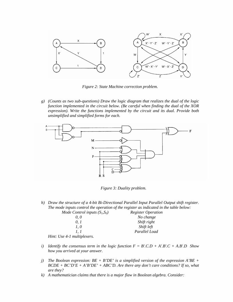
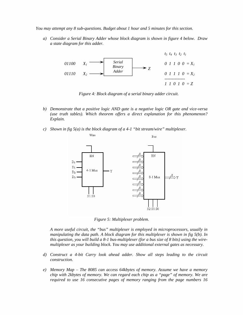
Figure 2: State Machine correction problem. g) (Counts as two sub-questions) Draw the logic diagram that realizes the dual of the logic
function implemented in the circuit below. (Be careful when finding the dual of the XOR expression). Write the functions implemented by the circuit and its dual. Provide both unsimplified and simplified forms for each.
Figure 3: Duality problem.
h) Draw the structure of a 4-bit Bi-Directional Parallel Input Parallel Output shift register. The mode inputs control the operation of the register as indicated in the table below:
Mode Control inputs (S1,S0) Register Operation 0, 0 No change 0, 1 Shift right 1, 0 Shift left 1, 1 Parallel Load
Hint: Use 4-1 multiplexers. i) Identify the consensus term in the logic function F = B'.C.D + A'.B'.C + A.B'.D Show
how you arrived at your answer.
j) The Boolean expression: BE + B’DE’ is a simplified version of the expression A’BE + BCDE + BC’D’E + A’B’DE’ + ABC’D. Are there any don’t care conditions? If so, what are they?
k) A mathematician claims that there is a major flaw in Boolean algebra. Consider:

A + A . B = A [since A + A . B = A . (1+B) = A . (1) = A] A . A + B = A [after applying the principle of duality] A + B = A [since A . A = A] Thus A + B = A which is clearly wrong. Find the flaw in the mathematician’s logic.
l) Give an example of a computation wherein edge triggering would lead to the correct
result, but level triggering would lead to an incorrect result. Illustrate your answer by way of timing diagrams.
m) Derive the Characteristic Equation Q* = S + R’Q of an S-R latch.
n) Bi-directional Buffer: In class you have learnt the operation of a Tri-state buffer. Such a
device acts as a unidirectional trap door – i.e. it allows data to flow in one direction. The data bus of a microprocessor is bi-directional; therefore it requires a buffer that allows data to flow in both directions. Using tri-state buffers and external gates, construct an 8-bit bi-directional buffer.
o) Assume you have a circuit that can manipulate 4-bit binary numbers. Two’s complement
arithmetic is the circuit’s mechanism for obtaining the negative of a number. (Hence subtraction is performed as addition of a negative number). Indicate whether the circuit will be able to perform the following additions:
1011 1101 0110
+ 0110 + 1010 + 0101 Provide the decimal value of the final answer in each of the above three cases. Q2] ECE231 Dinner - First Course: (8 x 4 = 32 points)
You may attempt any 8 sub-questions. Budget about 1 hour and 5 minutes for this section.
a) Consider a Serial Binary Adder whose block diagram is shown in figure 4 below. Draw a state diagram for this adder.
t5 t4 t3 t2 t1
01100 X1 0 1 1 0 0 = X1 Z 01110 X2 0 1 1 1 0 = X2
--------------
Serial Binary Adder
1 1 0 1 0 = Z
Figure 4: Block diagram of a serial binary adder circuit.
b) Demonstrate that a positive logic AND gate is a negative logic OR gate and vice-versa (use truth tables). Which theorem offers a direct explanation for this phenomenon? Explain.
c) Shown in fig 5(a) is the block diagram of a 4-1 “bit stream/wire” multiplexer.
Figure 5: Multiplexer problem.
A more useful circuit, the “bus” multiplexer is employed in microprocessors, usually in manipulating the data path. A block diagram for this multiplexer is shown in fig 5(b). In this question, you will build a 8-1 bus-multiplexer (for a bus size of 8 bits) using the wire-multiplexer as your building block. You may use additional external gates as necessary.
d) Construct a 4-bit Carry look ahead adder. Show all steps leading to the circuit
construction. e) Memory Map – The 8085 can access 64kbytes of memory. Assume we have a memory
chip with 2kbytes of memory. We can regard each chip as a “page” of memory. We are required to use 16 consecutive pages of memory ranging from the page numbers 16
through 31. What are the start and end addresses of this memory? Using 2-to-4 decoders, provide a scheme to achieve this. Show all address pin connections.
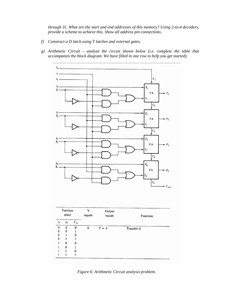
f) Construct a D latch using T latches and external gates. g) Arithmetic Circuit – analyze the circuit shown below (i.e. complete the table that
accompanies the block diagram. We have filled in one row to help you get started).
Figure 6: Arithmetic Circuit analysis problem.

h) In the 8085 microprocessor Pins A15-A8 and AD7 -AD0 are used as the 16-bit address bus and Pins AD7 -AD0 are used as the data bus. Initially, the pins carry the address of the memory to be accessed. Later on, the lower order pins act as the data bus. This would lead us to the architecture shown in figure 7. You need to design the “address hold” circuit. Use the ALE (Address Latch Enable) pin to guide the de-multiplexing i.e. show how the ALE might be used by the “address hold” circuit. [Hint: a hold circuit obviously involves a memory element since it can remember the address bits on the AD7 -AD0 pins long after they cease to exist. Pins AD7 -AD0 act as data bus once the addressing function is done].
Figure 7: Demultiplexing the Address and Data bus on the 8085.
i) Setup and Hold Times and D Flip Flops - We are given a positive edge triggered D Flip Flop with a setup time of 1 ns and a hold time of 1 ns. The clock signal has a period of 6 ns and has a 50% duty cycle. Complete the timing diagram in the figure below. Identify on the timing diagram where Q will be metastable/unstable using the convention taught in the book and in lecture. Remember that a positive edge triggered flip flop has the potential to come out of a metastable/unstable state at each rising edge of the clock. If it looks to you like the input satisfies the setup and hold requirements, then it most likely does.
Figure 8: Timing Diagram problem.

Q3] ECE231 Dinner - Second Course: (3 x 8 = 24 points) You must attempt sub-questions (c), (d) and either (a) or (b). Budget 50 minutes for this section.
(a) For the circuit shown in the figure 9 below, determine transition/output and state/output tables. What type (Mealy/Moore) of machine is this? Explain.
Figure 9: Circuit for question 3(a).
(b) (1) Use a 74x163 and a decoder of your design to implement a decade (modulo-10) counter. Instead of using states 0-9 of the counter, use states 6-15. On the diagram below draw the logic you used to send the ‘163 to state 6 from state 15. (2) Design a decoder that maps 6->0, 7->1, 8->2, …14->8, 15->9. When designing the decoder, consider input combinations 0000 to 0101 as don't care inputs. Your decoder should have only 4 inputs and 4 outputs with no enable inputs.
Figure 10: Decade Counter problem.

(c) Show that the following system is functionally complete: f (A, B, C) = A’BC + AB’ + B’C’.
(d) Fill out the timing diagram for a 4-bit ripple adder below. The gate-level circuit diagram
of each full adder is as given here. Assume the propagation delays tpLH = tpHL = 15 ns for the NAND gates and tpLH = tpHL = 30 ns for the XOR gates used in each full adder. Given your knowledge of delays in ripple adders and the timing diagram you drew above, how long after S0 is calculated is S3 calculated? (Hint: if you aren’t confident about your timing diagram above, you can check your answer mathematically. Don’t make this problem harder than it is!)
Figure 11: Full Adder circuit and Block Diagram.
Figure 12: 4-bit Ripple Adder circuit.

Figure 13 (a)
Figure 13 (b)
Figure 13 (c)
Figure 13 (d)

Q4] ECE231 Dinner - Main Course: (1 x 16 = 16 points) Earlier, you got the feel for an Arithmetic Circuit. Now we will design a rudimentary
computer. This tutorial will lead step-by-step through the creation process. Computer Specification:
The system consists of a memory unit, seven registers and two decoders. The memory unit
has 256 words of 8 bits each. This is very small for a real computer, but sufficient to demonstrate the basic operations found in most computers. Instructions and Data are stored in the memory unit, but all information processing is done in the registers. Table 1 provides details about the registers.
Table 1: List of registers for the simple computer Symbol Number
of bits Name of Register Function
MAR 8 Memory address register Holds address for memory MBR 8 Memory buffer register Holds contents of memory word A 8 Accumulator Processor register R 8 R register Processor register PC 8 Program Counter Holds address of instruction IR 8 Instruction Register Holds current operation code T 3 Timing Counter Sequence generator
PC, IR and T are part of the control unit. IR receives the operation code of instructions. The decoder associated with this register supplied one output for each operation code encountered. Thus q1 = 1 if the operation is binary 1, q2 = 1 if the operation is binary 2, and so on. Register T is needed to supply with timing variables t0 through t7. This counter is incremented with every clock pulse, but it can be cleared at any time to start a new sequence from t0.
PC goes through a step-by-step counting sequence and causes the computer to read successive instructions previously stored in memory. PC always holds the address of the next instruction in memory. To read an instruction, the contents of PC are transferred into MAR and a memory-read cycle is initiated. PC is then incremented by 1 so that it holds the next address in the sequence of instructions. An operation code read from memory into MBR is then transferred into IR. If the memory–address part of an instruction is read into MBR, this address is transferred into MAR to read the operand. Thus, MAR can receive addresses either from PC or MBR. Although an 8-bit IR allows us to specify up to 256 instructions, our simple computer has only three. These are described in the table below. The Mnemonic column could for example be the Assembly Language instructions generated by the Compiler of a High Level Programming Language such as C++. The first column could represent the machine language instructions generated from the assembly language by an Assembler.
Table 2: Three instructions for the simple computer Operation
Code Mnemonic Description Function
00000001 MOV R Move R to A A ← R 00000010 LDI OPRD Load OPRD into A A ← OPRD 00000011 LDA ADRS Load operand specified by
ADRS into A A ← M[ADRS]

Instruction Fetch Cycle: PC must be initialized to contain the first address of the sequence of program instructions stored in memory. When a start switch is activated, the PC fetches successive instructions. Each fetch is accomplished by a set of steps called Microinstructions as shown below: t0: MAR ← PC transfer op-code address t1: MBR ← M, PC ← PC + 1 read op-code, increment PC t2: IR ← MBR transfer op-code into IR
PC was incremented in clock cycle t1 to prepare it to fetch the next instruction in the memory. Once the instruction is brought in the IR, the control unit will decode it. The timing variables t0, t1, and t2 out of the timing decoder are used as control functions to sequence the micro-operations for reading an op-code and placing it in the IR. It is assumed that T starts from a value of 000, which produces a t0 timing variable out of the decoder. T is incremented every clock pulse and automatically produces the next timing variable in sequence. The hardware constraint is that only MAR and MBR can communicate with the memory, hence PC and IR had to use these intermediaries as shown in the microinstructions above. The fetch cycle is common to all instructions. The micro-operations and control functions that follow the fetch cycle are determined in the control section from the decoded operation code. This is available from outputs qi, I = 1, 2, 3, … in the operation decoder. Execution of Instructions: During timing variable t3 the op-code is in IR and one output of the decoder is equal to 1. (q1 or q2 or q3 corresponding to the 3 instructions offered by our computer). The control uses the qi variables to determine the next micro operations in sequence. Let MOV use q1, LDI use q2 and LDA use q3. Execution of the MOV instruction could then be coded as the following single micro operation: q1t3: A ← R, T ← 0 transfer R to A and Reset T for next cycle. By clearing T, control goes back to produce timing variable t0 and thus starts the fetch cycle again to read the next op-code in sequence. Remember that PC was already incremented during the fetch cycle to point to the address of the next instruction in memory. Your first assignment is to write microinstructions for the LDI and LDA instructions. Ie you will complete the table given below.
Table 3: Register transfer statements for the simple computer Fetch t0 MAR ← PC t1 MBR ← M, PC ← PC + 1 t2 IR ← MBR MOV q1t3 A ← R, T ← 0 LDI q2t3 MAR ← PC q2t4 q2t5 LDA q3t3 MAR ← PC q3t4 q3t5 q3t6 q3t7

Computer Design: We now create the hardware specification for our computer using the entries made in the
table above. For example, since MAR ← PC occurs 3 times in the table above, we arrive at the following hardware specification: t0 + q2t3 + q3t3: MAR ← PC
t0 + q2t3 + q3t3 is actually a combinational circuit (say x1) as shown below.
OR AND
PC
MAR OR
t0
load t3
q2
x1
q3
Figure 14: Implementation of x1: MAR ← PC.
Only for the duration that x1 is active is the MAR circuit enabled. It is only during this time that MAR can successfully read the value of the PC. Your second assignment is to create the hardware specifications for the remaining micro-operations. Ie complete the table shown below.
Table 4: Hardware specification for the simple computer
x1 = t0 + q2t3 + q3t3 MAR ← PC x2 = MAR ← MBR x3 = PC = PC + 1 x4 = MBR ← M x5 = A ← MBR x6 = A ← R x7 = T ← 0 x8 = IR ← MBR
Each of these eight specifications will lead to a different combinational circuit, which will operate (enable) some of the computer circuitry. We group these eight circuits into a single box (called the combinational circuit), which drive the computer. We now wire all the system components (memory unit, registers and decoders) together and voila our computer is ready! The correct hardware specification will lead to the rudimentary computer shown below. (Use this to check the correctness of your Register transfer statements and hardware specifications). Note that the circuit for x1 is no longer directly connected to the MAR but rather it is OR-ed with x2 and then connected to MAR. This is because we observe from the first two entries in table 4 that MAR can obtain its value from PC or from MBR. The MUX serves to route one of the two values to MAR. Circuit x1 drives the MUX to select value from PC while absence of x1 drives MBR to MAR via MUX. Logic circuitry for the rest of the circuit can be similarly explained.
Naturally, this is too simplistic a computer. A real computer would have many more complex instructions in its instruction set. Still, we have gotten you off the starting blocks!