The Potential Role of Modeling and Simulation in PV … · The Potential Role of Modeling and...
26
The Potential Role of Modeling and Simulation in PV Industry BAPVC Workshop and Industry Board Meeting, January 12, 2012 Muhammad Alam and Mark Lundstrom Birck Nanotechnology Center Purdue University 1
Transcript of The Potential Role of Modeling and Simulation in PV … · The Potential Role of Modeling and...

The Potential Role of
Modeling and
Simulation in PV Industry
BAPVC Workshop and Industry Board Meeting, January 12, 2012
Muhammad Alam and Mark Lundstrom
Birck Nanotechnology Center
Purdue University
Simulation in PV Industry
1

Outline
Historical role of Modeling and Simulation in PV industry
Opportunities to contribute to end-to-end modelingExample 1: Organic Solar CellsExample 2: Shunt Conduction
How to connect industry and academia by nanohub--- Simulation tools --- Tutorials and educational material
Conclusions

Thermodynamic Limit of Efficiency
0 ( ,) 0, )( phS SEg SI D E n dq E c ETµ∞
× ∆= =×Ω ×∫
( )0outSQ
i n
t
n i
spoVP II
P Pη
−= =
(( , , ))sp D DEg ph Dq D EI qVE T dcn Eµ−∆
∞Ω ∆ =××= ∫
W. Shockley, H. Queisser,JAP, 32(3), 510, 1961.
30.5 1 1.5 2 2.5 30
0.05
0.1
0.15
0.2
0.25
0.3
0.35
Effi
cien
cy
Eg (eV)
SQE
g - E
Cross=0.1 eV
Eg - E
Cross=0.3 eV
Eg - E
Cross=0.5 eV
i nn iP P
Interface recomb
qV

Efficiency Limits of Silicon Solar Cells
“Why Don’t We Have a 30% Efficient Si Solar Cell?” J.L. Gray and R.J. Schwartz, PVSC 1985
At a time of 19-20% cell…
4
1977
“Why We Will Have a 30% Efficient Si Solar Cell” R.M. Swanson, PVSC 1989
Opportunities for optimization of cell performance

Opportunities for Design
Back Contact Solar Cell (R.J. Schwartz, IEDM, 1975)
5
R.M. Swanson, “Point-contact solar cells: modeling and experiment” Solar Cells, 1985.

Exploring New Approaches
G. Lush & M. Lundstrom, “Thin film approaches for high-efficiency III-V cells” Solar Cells, 30 337 (1991).
G. B. Lush, et. al., “Microsecond lifetimes and low interface recombination velocities in moderately doped n-GaAsthin films,” APL, 61, 2441, 1992.
G.B. Lush, et al.,” Thin-film GaAs Solar Cells by Epitaxial Lift-off,” PVSC, 1993.
6
Cells by Epitaxial Lift-off,” PVSC, 1993.
Brendan M. Kayes, et al.,“27.6% Conversion Efficiency, A New Record for Single-junction Solar Cells Under 1-Sun Illumination,” PVSC 2011.
28.5% at 1-Sun

Too Complex to Model?
8
10
/cm
2 )
Nat. Mat, 2009
Organic Solar Cell CZTS
7
101
102
2
4
6
8
Anneal Time (min)
J SC
(mA
/cm
ta(opt)
(b)CIGS
Ramanathan , 2003
Guo , 2003
Grain boundaries, percolating cluster, anneal dependence, Na dependence …… problems beyond modeling?

Elements of end-to-end modeling
1) Process/Materials
2) Device5) Systems6) Software (ADEPT,
3) Characterization4) Reliability
End-to-end modeling of process/device/reliability/systems
Approaches applicable to multiple materials
Embedded in open source software platform
6) Software
Platform(ADEPT,
AMPS, PC1D)
8
(SCAPS)
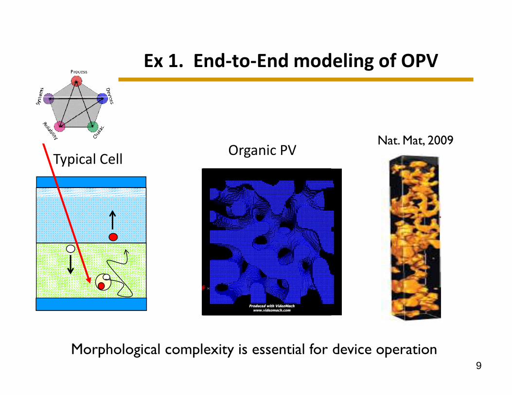
Ex 1. End-to-End modeling of OPV
Organic PVTypical Cell
Nat. Mat, 2009
9
Morphological complexity is essential for device operation

Process Model: Demixing & Self-Organization
Polymer-A(Donor)
Solvent Polymer-B(Acceptor)
Free Energy, fmix
-0.2
0
0.2
0.4
ØA ØD100100100100100100100100
10
Phase Separation occurs through Spinodal Decomposition
10-15 min @125-150C Cahn-Hilliard Equation
2 40 2
ϕ κ ϕϕ
∂ ∂= ∇ − ∇ ∂ ∂
fM
t
Composition, Ø
Free Energy,
0 0.5 1-0.4
-0.2
X (nm)
Y (
nm
)
0 50 100
50
0
X (nm)
Y (
nm
)
0 50 100
50
0
X (nm)
Y (
nm
)
0 50 100
50
0
X (nm)
Y (
nm
)
0 50 100
50
0
X (nm)
Y (
nm
)
0 50 100
50
0
X (nm)
Y (
nm
)
0 50 100
50
0
X (nm)
Y (
nm
)
0 50 100
50
0
X (nm)
Y (
nm
)
0 50 100
50
0

Device Simulation & Experiments
00 Experiment [9]
4 min
Simulation (a) (b)
Experiment Simulation
11
0 0.2 0.4 0.6-10
-5
Voltage(V)0 0.2 0.4 0.6
-10
-5
Voltage(V)
J (m
A/c
m2 )
4 min
40 min
90 min
120 min
4 min
40 min
90 min
120 min
The limits of Jsc, Voc, and FF can be easily understood
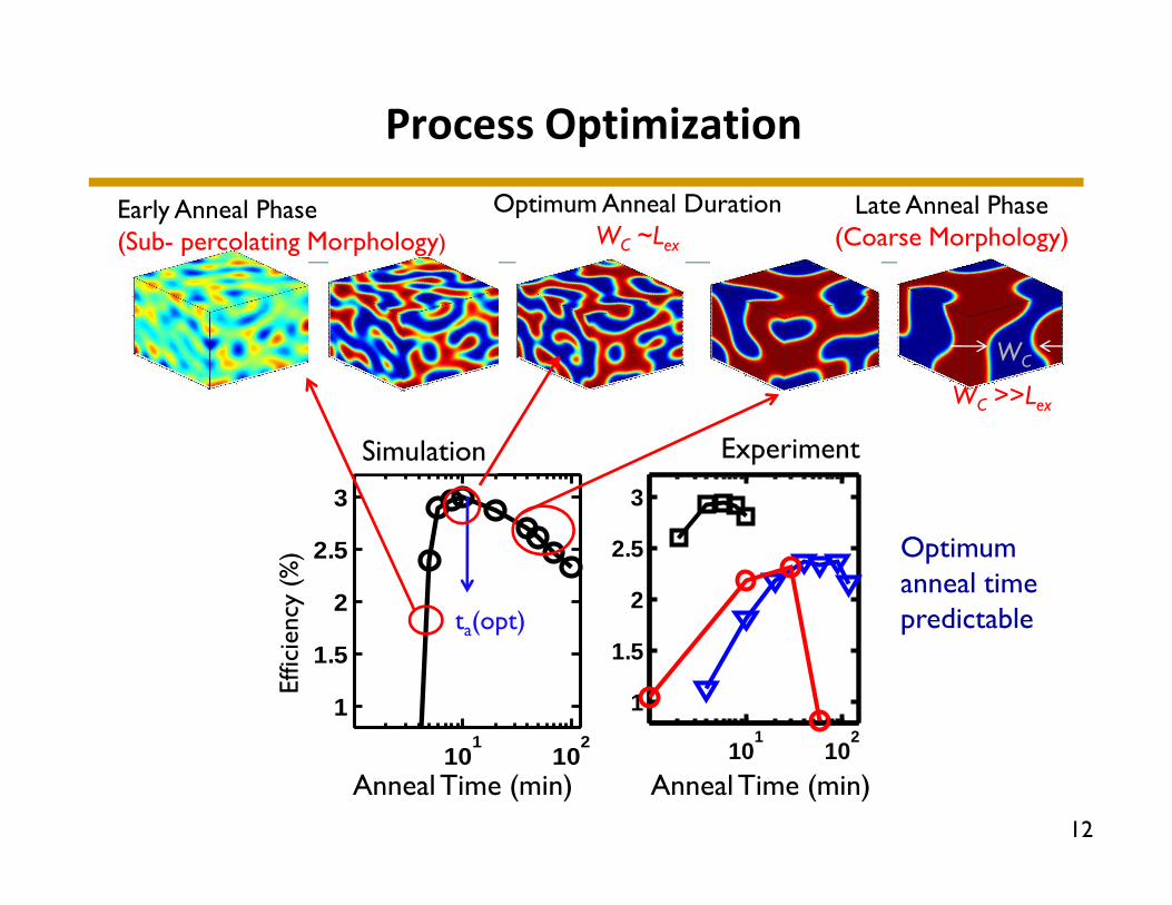
Process Optimization: Annealing
Experiment Simulation
Optimum Anneal DurationWC ~Lex
WC
Late Anneal Phase(Coarse Morphology)
Early Anneal Phase(Sub- percolating Morphology)
WC >>Lex
101
102
1
1.5
2
2.5
3
Anneal Time (min)
Experiment
Anneal Time (min)
Efficiency (%)
101
102
1
1.5
2
2.5
3
ta(opt)
Simulation
12
Optimum anneal time predictable

JSC: Morphology & ReliabilityP
roce
ssin
g
Anneal duration, ta
Ta
=120
0 C
C
Stress duration, ts
102
103
3
3.5
4
4.5
5
J SC(m
A/cm
2)
ta (opt)
Low T
High T
Ts
=120
0 CStr
ess
Ts
=100
0 C
WC
102
103
Anneal time (min)
100
101
102
0.2
0.4
0.6
0.8
1 Ta= 500
J SC(norm
)
Stress time (h)
Ta= 800
SCJ ∝∝∝∝ n
eff opD t−−−−
∝∝∝∝ ex
C
L
W
Analytical Model
exp( / )eff A opD E kT∝ −∝ −∝ −∝ −

~ tn
thj
Anneal time
(b)Ex 1: End-to-End modeling of OPV
1) Process Model2) Device Sim.
0.8
1
(no
rm)
Ts= 800, 700, 600, 500 C
Electron
2) Device Sim.
3) Characterization4) Optimization
0 0.2 0.4 0.6-10
-5
0
Voltage(V)
J SC
(mA
/cm
2 ) 4 min
10 min20 min100 min
20
40
60
101
102
2
4
6
8
10
Anneal Time (min)
J SC(m
A/cm
2)
ta(opt)
5) Reliability
100
101
102
0.2
0.4
0.6
0.8
StressTime (h)
J SC
(no
rm)
exp. data [5]
14

Ex 2: ‘Technology-Agnostic’ approach to PV devices
P
D
R
S
C
15

Ex 2: ‘End-to-end Model of Shunt Conduction
AZO
a-Si:Hi
n
Process Model
p
P
D
R
S
C
16
(i)
(ii)
Device Model
CharacterizationReliability Model

Gap between Cell vs. Module Efficiency
0
5
10Power Distribution (mW)
0.75
0.99
CD
F (
norm
al)
1Ω/sq.4Ω/sq.8Ω/sq.
10X10 cm2
P
D
R
S
C
17
-15
-10
-5
0
Shunt distribution and series Rs explain the efficiency gap
6 7 8 9 10
0.01
0.25
0.75
Submodule Efficiency (%)
CD
F (
norm
al)
Cell
10X10 cm2

ERI-NPT Summary of research results 2010-11
1) Process
Model10
20
30
40
50
60
0
20
40
60
80
100
h(i,t
)
a-Si poly-crystal Image analysis
2) Devices:
Pol
ymer
thic
knes
s (n
m)
sc(max)
200
250
Database5) HIT Cell
a-Si p+-emitter
a-Si i-layer
c-Si n type
Pol
ymer
thic
knes
s (n
m)
ITO thickness (nm)100 200 300 400
50
100
150
200
CIGS with GB Optics
4) Compact model
Shunt statistics Module efficiency
Compact model
Si n type-B
ase
a-Si i-layer
a-Si n+-BSF c-si HIT-cell
3) Characterization:
18

Outline
Historical role of Modeling and Simulation in PV industry
Opportunities to contribute to end-to-end modelingExample 1: Organic Solar CellsExample 2: Shunt Conduction Example 2: Shunt Conduction
How to connect industry and academia by nanohub--- Simulation tools --- Tutorials and educational material
Conclusions

Network for Computational Nanotechnology
Mission:
Research that helps move nanoscience to nanotechnology to nanomanufacturing.
Infrastructure to:
• connect experts in theory, modeling, and
Key strategy:
Cyber-infrastructure
• connect experts in theory, modeling, and simulation and engage experimentalists
• disseminate software, insights and understanding, and research methods
• promote cross-disciplinary and simulation-based research and education
Established by NSF in 2002. 10-year, ~$30M investment
20

nanoHUB.org
a major, international resource for nanotechnology
>180,000 / year
enabled by the HUBzero platform for simulation, learning, and collaboration
1994
• open source platform
30% US / 24% Eur. / 35% Asia / 10% other
21

PVhub
https://nanohub.org/groups/pv
Welcome to PVhub!PVhub is a resource for the photovoltaics community. Our mission is to provide access to live simulations and resources for education and research. PVhub is an initiative of the Network for Photovoltaic Technology and the Network for Computational Nanotechnology. Technology and the Network for Computational Nanotechnology.
“I’d put my money on the sun and solar energy. What a source of power! I hope we don’t have to wait until oil and coal run out before we tackle that.” – Thomas Edison, 1931
22

Web enabled Tools
ADEPT PV Analyzer
OPV tool
PV Panel Sim
OPV tool
23

Education
24
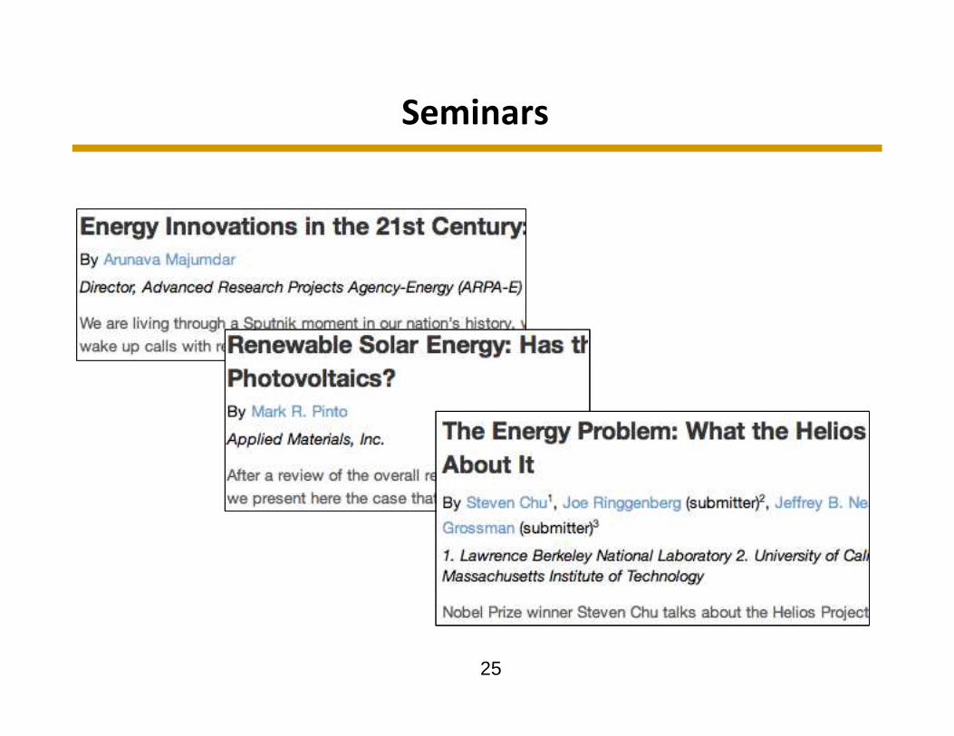
Seminars
25

The Opportunity
Lessons from electronics:-importance of end-to-end modeling-need for shared platforms-M and S can have great impact
Strategy:
26
Strategy:-seek “technology agnostic solutions”-develop tools to solve problems-share tools with collaborators and sponsors-connect industry needs to university research-demonstrate the value of shared, pre-competitive research
Questions/comments: [email protected]