The p-n Homojunction -...
29
February 2, 2012 The University of Toledo, Department of Physics and Astronomy SSARE, PVIC Principles and Varieties of Solar Energy (PHYS 4400) and Fundamentals of Solar Cells (PHYS 6980) The p-n Homojunction
-
Upload
nguyendiep -
Category
Documents
-
view
215 -
download
0
Transcript of The p-n Homojunction -...
February 2, 2012The University of Toledo, Department of Physics and Astronomy
SSARE, PVIC
Principles and Varieties of Solar Energy (PHYS 4400)and
Fundamentals of Solar Cells (PHYS 6980)
The p-n Homojunction

H. Föll: http://www.tf.uni-kiel.de/matwis/amat/semi_en/kap_2/backbone/r2_2_4.html
Consider the the band diagram for a homojunction, formed when two bits of the same type of semiconductor (e.g. Si) are doped p and n type and then brought into contact.
Electrons in the two bits have different electrochemical potentials (i.e. different Ef’s)
Charge transfer occurs at contact(electron go down from the vacuum level, holes go “up”)
At equilibrium, there is no net transport (Ef is constant throughout the device)
VBI
VBI
The p-n Homojunction

R. Wang: http://fourier.eng.hmc.edu/e84/lectures/ch4/node1.html
at/during contact
At equilibrium
Space charge region (SCR) or Depletion region
Charge of -1 relative to the other atoms (NA
-)
Charge of +1 relative to the other atoms (ND
+)

http://www-tcad.stanford.edu/tcad/education/anim.html
p-type n-typeEfermi
Band gap
Vbuilt In
Majority carriers diffuse across the Depletion Region (because the electric field is reduced), where they become minority carriers and recombine (a.k.a. minority carrier injection)
a.k.a. Reverse Saturation Current: minority carriers drift across the Depletion Region with the assistance of the larger electric field, where they become manority carriers and recombine
E
aka junction voltage or barrier voltage or contact potential
p-type n-type
In the dark (equilibrium)
http://pveducation.org
p-type n-type
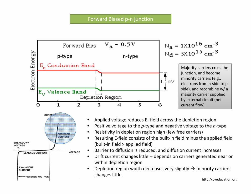
Forward Biased p-n junction
• Applied voltage reduces E- field across the depletion region• Positive voltage to the p-type and negative voltage to the n-type• Resistivity in depletion region high (few free carriers)• Resulting E-field consists of the built-in field minus the applied field
(built-in field > applied field)• Barrier to diffusion is reduced, and diffusion current increases• Drift current changes little -- depends on carriers generated near or
within depletion region• Depletion region width decreases very slightly minority carriers
changes little.
Majority carriers cross the junction, and become minority carriers (e.g., electrons from n-side to p-side), and recombine w/ a majority carrier supplied by external circuit (net current flow).
http://www-tcad.stanford.edu/tcad/education/anim.html
p-type
n-type
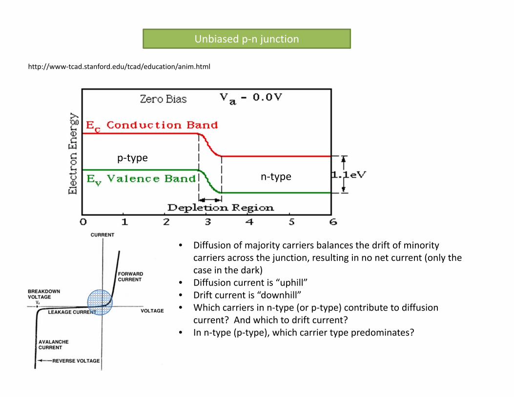
Unbiased p-n junction
• Diffusion of majority carriers balances the drift of minority carriers across the junction, resulting in no net current (only the case in the dark)
• Diffusion current is “uphill”• Drift current is “downhill”• Which carriers in n-type (or p-type) contribute to diffusion
current? And which to drift current?• In n-type (p-type), which carrier type predominates?
http://pveducation.org
p-type n-type
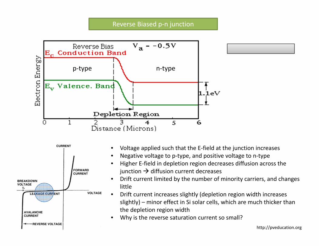
Reverse Biased p-n junction
• Voltage applied such that the E-field at the junction increases• Negative voltage to p-type, and positive voltage to n-type• Higher E-field in depletion region decreases diffusion across the
junction diffusion current decreases• Drift current limited by the number of minority carriers, and changes
little• Drift current increases slightly (depletion region width increases
slightly) – minor effect in Si solar cells, which are much thicker than the depletion region width
• Why is the reverse saturation current so small?

http://pveducation.org
Reverse Biased p-n junction (breakdown, avalanche current)
p-type n-type
Va < -1.0 V In breakdown, electrons can tunnel from the p-type material valence band through the depletion region material to contribute to large negative current flow (electrons to the right through n-type material)
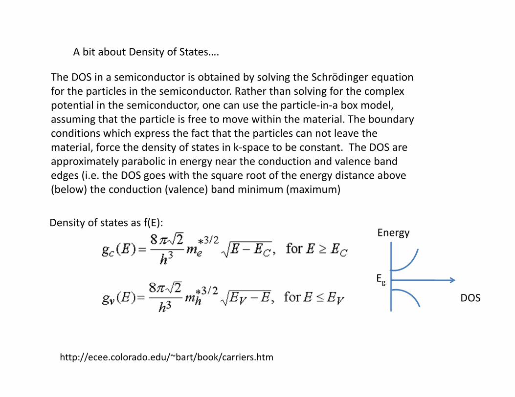
A bit about Density of States….
The DOS in a semiconductor is obtained by solving the Schrödinger equation for the particles in the semiconductor. Rather than solving for the complex potential in the semiconductor, one can use the particle-in-a box model,assuming that the particle is free to move within the material. The boundary conditions which express the fact that the particles can not leave the material, force the density of states in k-space to be constant. The DOS are approximately parabolic in energy near the conduction and valence band edges (i.e. the DOS goes with the square root of the energy distance above (below) the conduction (valence) band minimum (maximum)
http://ecee.colorado.edu/~bart/book/carriers.htm
DOS
Energy
Eg
Density of states as f(E):
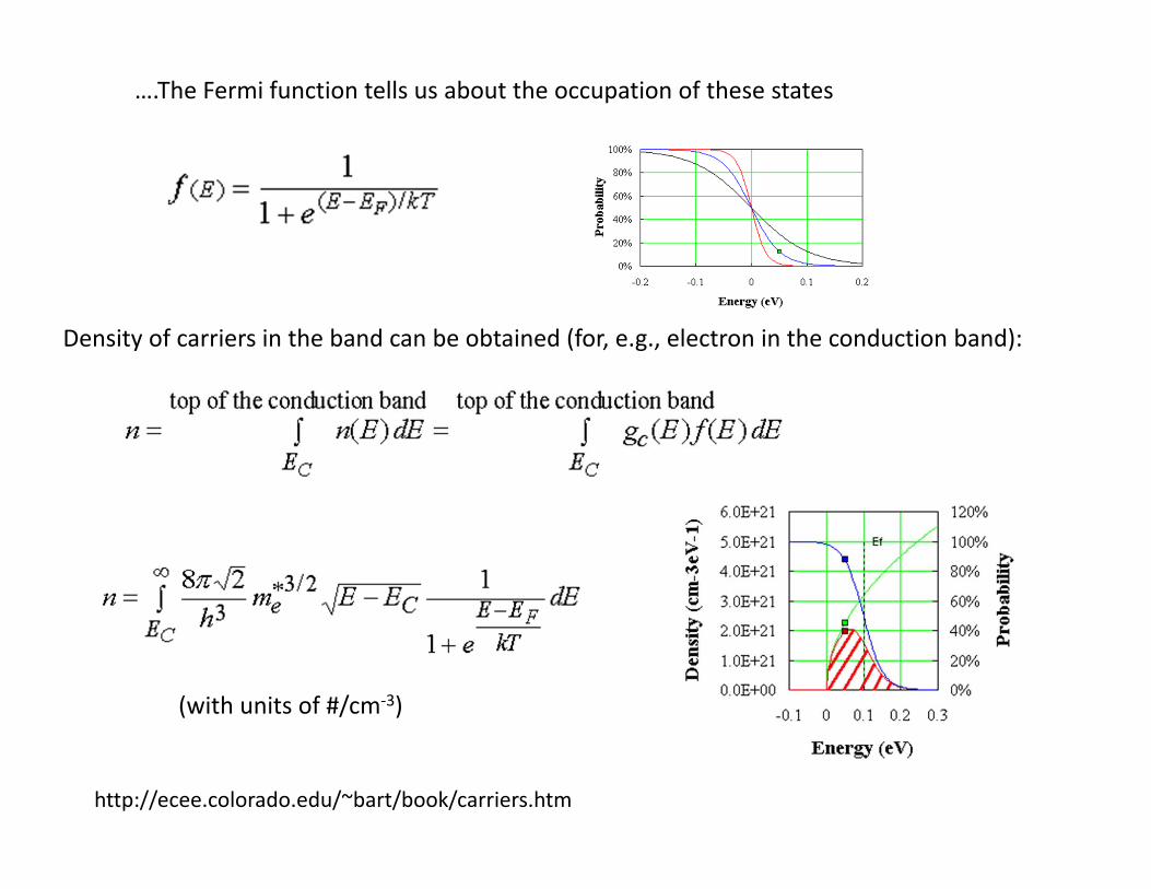
….The Fermi function tells us about the occupation of these states
Density of carriers in the band can be obtained (for, e.g., electron in the conduction band):
http://ecee.colorado.edu/~bart/book/carriers.htm
(with units of #/cm-3)
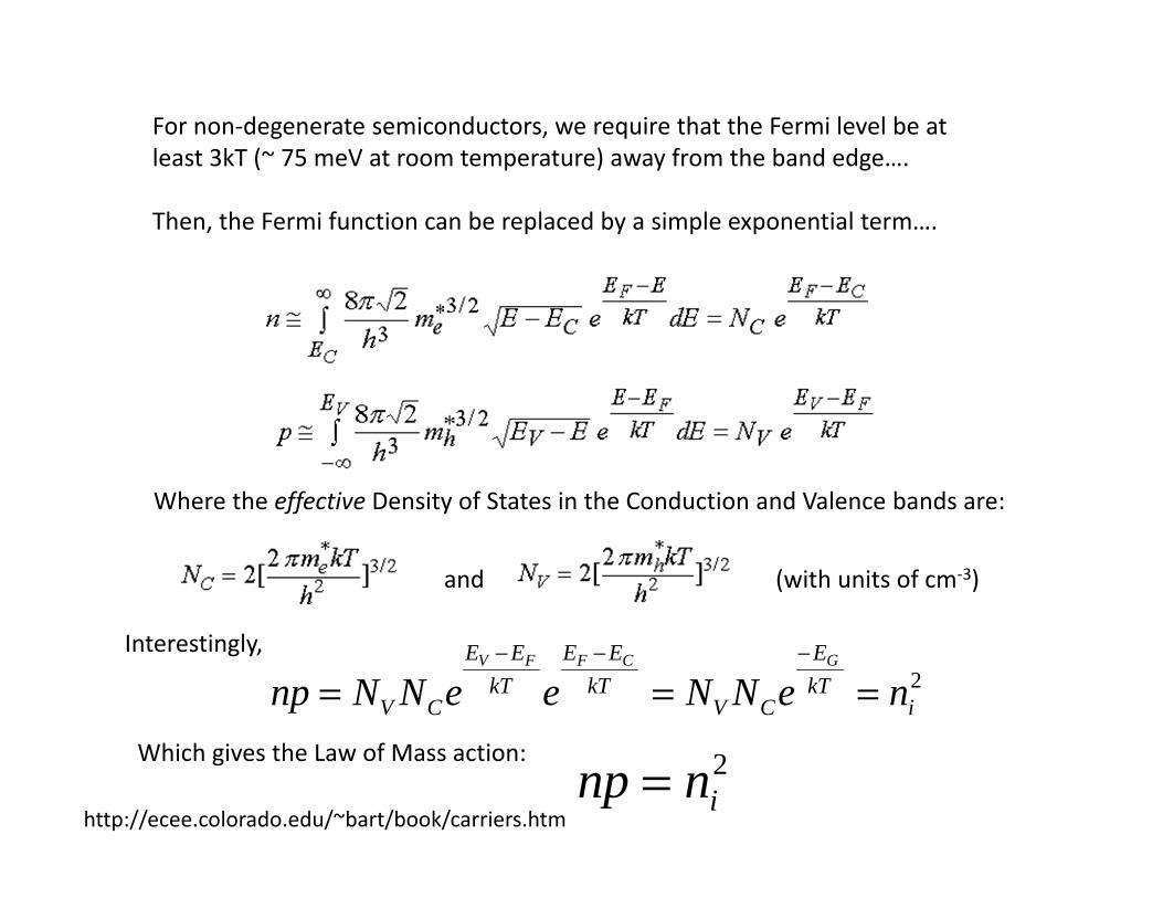
For non-degenerate semiconductors, we require that the Fermi level be at least 3kT (~ 75 meV at room temperature) away from the band edge….
Then, the Fermi function can be replaced by a simple exponential term….
Where the effective Density of States in the Conduction and Valence bands are:
and (with units of cm-3)
np = NV NCeEV − EF
kT eEF − EC
kT = NV NCe−EG
kT = ni2
Interestingly,
np = ni2Which gives the Law of Mass action:
http://ecee.colorado.edu/~bart/book/carriers.htm

np = NV NCeEV − EF
kT eEF − EC
kT = NV NCe−EG
kT = ni2
ni = NV NC e−EG
2kT
Ei
p-type n-typeintrinsic
Ei –EF Ei -EF
EF -Ec
ni ranges from 1013 #/cc for Ge (Eg = 0.66eV)to 106 #/cc for GaAs (Eg = 1.42 eV)
A positive number
for Si: ni ~ 1 x 1010 cm-3
NC = 3.2 x 1019 cm-3
NV = 1.8 x 1019 cm-3
A negative numberA negative number A positive number
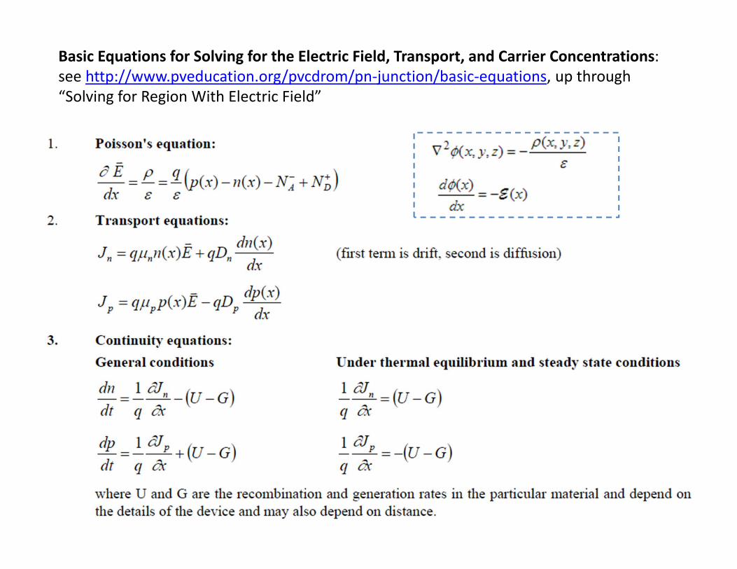
Basic Equations for Solving for the Electric Field, Transport, and Carrier Concentrations:see http://www.pveducation.org/pvcdrom/pn-junction/basic-equations, up through “Solving for Region With Electric Field”
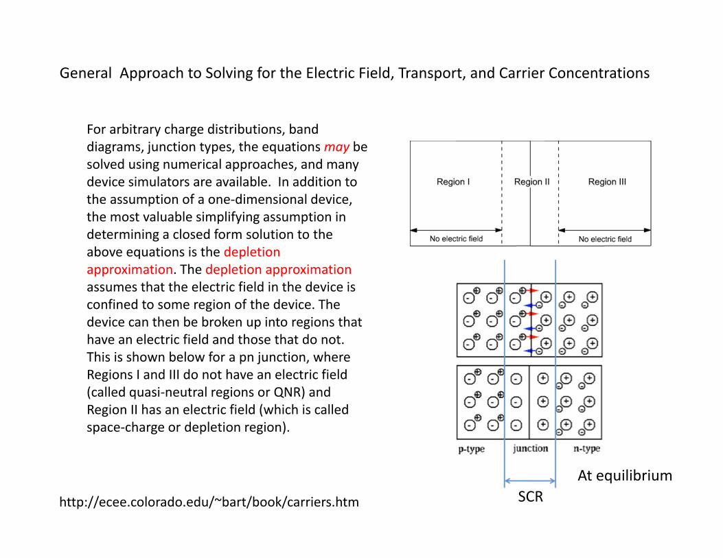
General Approach to Solving for the Electric Field, Transport, and Carrier Concentrations
For arbitrary charge distributions, band diagrams, junction types, the equations may be solved using numerical approaches, and many device simulators are available. In addition to the assumption of a one-dimensional device, the most valuable simplifying assumption in determining a closed form solution to the above equations is the depletion approximation. The depletion approximation assumes that the electric field in the device is confined to some region of the device. The device can then be broken up into regions that have an electric field and those that do not. This is shown below for a pn junction, where Regions I and III do not have an electric field (called quasi-neutral regions or QNR) and Region II has an electric field (which is called space-charge or depletion region).
At equilibriumSCRhttp://ecee.colorado.edu/~bart/book/carriers.htm
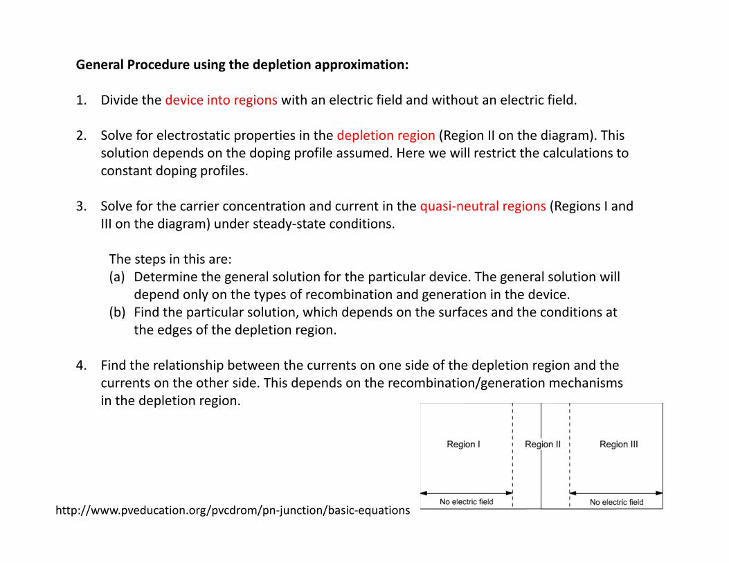
General Procedure using the depletion approximation:
1. Divide the device into regions with an electric field and without an electric field.
2. Solve for electrostatic properties in the depletion region (Region II on the diagram). This solution depends on the doping profile assumed. Here we will restrict the calculations to constant doping profiles.
3. Solve for the carrier concentration and current in the quasi-neutral regions (Regions I and III on the diagram) under steady-state conditions.
The steps in this are:(a) Determine the general solution for the particular device. The general solution will
depend only on the types of recombination and generation in the device.(b) Find the particular solution, which depends on the surfaces and the conditions at
the edges of the depletion region.
4. Find the relationship between the currents on one side of the depletion region and the currents on the other side. This depends on the recombination/generation mechanisms in the depletion region.
http://www.pveducation.org/pvcdrom/pn-junction/basic-equations

Basic Equations for Solving for the Electric Field, Transport, and Carrier Concentrations
http://www.pveducation.org/pvcdrom/pn-junction/basic-equations

1. Depletion approximation: the electric field is confined to a particular region.2. No free carriers (n(x), p(x) = 0 ) in depletion region.3. We can assume no free carriers since the electric field sweeps them out of the
depletion region quickly. No free carriers means (1) transport equations drop out and (2) no recombination or generation, so the continuity equation becomes:
This means that Jn is constant across the depletion region. Similarly, Jp is also constant across the depletion region.
4. Abrupt or step doping profile (NA-, ND+ are constant).
5. All dopants are ionized NA-= NA, ND
+ = ND).6. One-dimensional device.
Solving for Region With Electric Field
http://www.pveducation.org

Solution
The only equation left to solve is Poisson’s Equation, with n(x) and p(x) =0, abrupt doping profile and ionized dopant atoms. Poisson’s equation then becomes:
Where ε =ε0 εs , ε0 is the permittivity in free space, and εs is the permittivity in the semiconductor and xp and xn are the edges of the depletion region in the p- and n-type side respectively, measured from the physical junction between the two materials. The electric field then becomes
http://www.pveducation.org

The integration constants C1 and C2 can be determined by using the depletion approximation, which states that the electric field must go to zero at the boundary of the depletion regions. This gives:
Solution (continued…)
http://www.pveducation.org
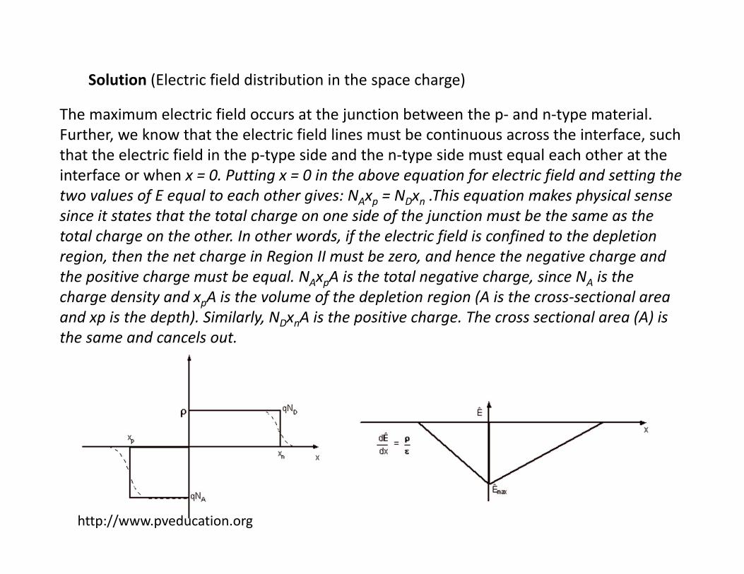
The maximum electric field occurs at the junction between the p- and n-type material. Further, we know that the electric field lines must be continuous across the interface, such that the electric field in the p-type side and the n-type side must equal each other at the interface or when x = 0. Putting x = 0 in the above equation for electric field and setting the two values of E equal to each other gives: NAxp = NDxn .This equation makes physical sense since it states that the total charge on one side of the junction must be the same as the total charge on the other. In other words, if the electric field is confined to the depletion region, then the net charge in Region II must be zero, and hence the negative charge and the positive charge must be equal. NAxpA is the total negative charge, since NA is the charge density and xpA is the volume of the depletion region (A is the cross-sectional area and xp is the depth). Similarly, NDxnA is the positive charge. The cross sectional area (A) is the same and cancels out.
Solution (Electric field distribution in the space charge)
http://www.pveducation.org
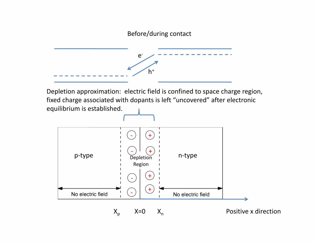
Depletion approximation: electric field is confined to space charge region, fixed charge associated with dopants is left “uncovered” after electronic equilibrium is established.
X=0
p-type n-typeDepletion Region
Xp Xn Positive x direction
+-
-
-
-
+
+
+
Before/during contact
e-
h+

R. Wang: http://fourier.eng.hmc.edu/e84/lectures/ch4/node1.html
at/during contact
At equilibrium
Space charge region (SCR) or Depletion region
Charge of -1 relative to the other atoms (NA
-)
Charge of +1 relative to the other atoms (ND
+)
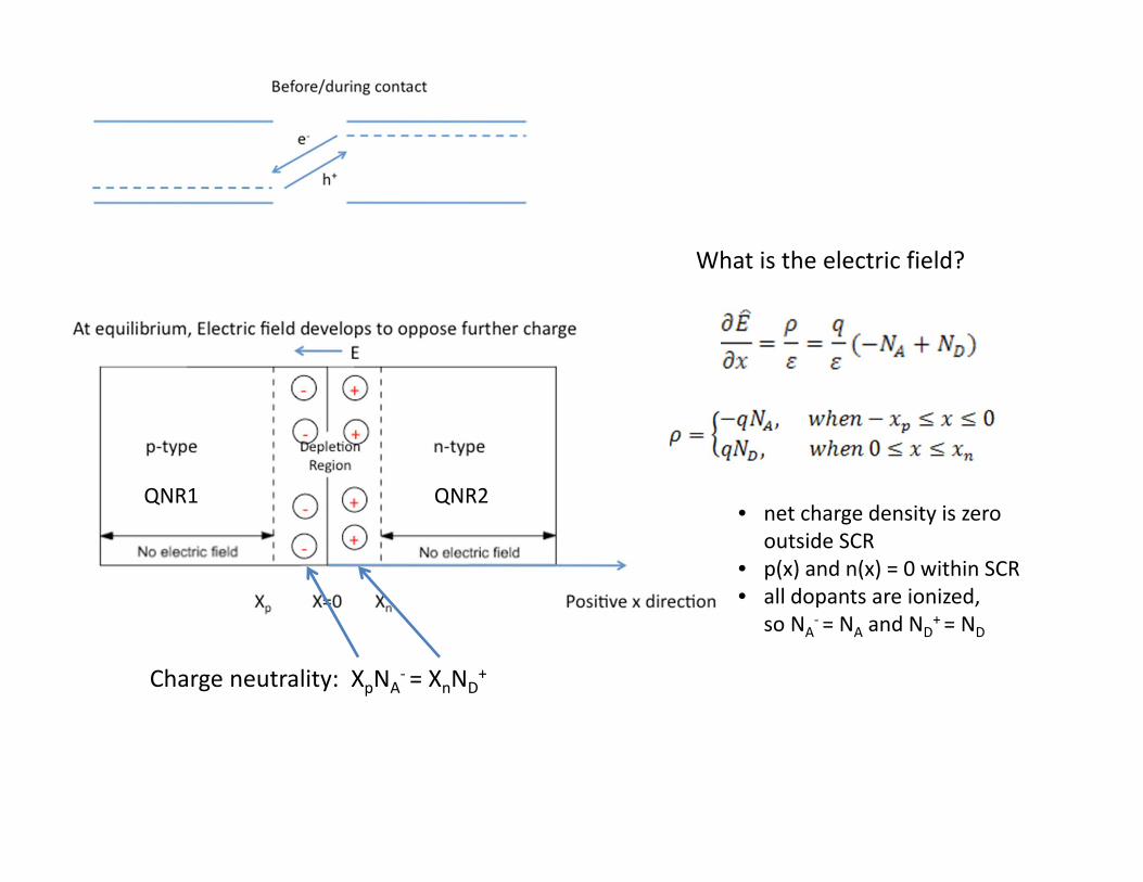
Charge neutrality: XpNA- = XnND
+
What is the electric field?
QNR1 QNR2• net charge density is zero
outside SCR• p(x) and n(x) = 0 within SCR• all dopants are ionized,
so NA- = NA and ND
+ = ND

Bringing back the Boundary Conditions(E goes to zero at boundaries of DR)

The two parts of the solution must give the same value for E when x = 0
so –NAxp = -NDxn, which is the charge neutrality relation written earlier
xnxp
Plots shown for NA ≠ ND|E|max at x = 0

What is the potential distribution? • Integrate the electric field over distance.
Since we are interested in the potential difference, we can set the voltage on the p-type side to be zero, such that at x= −xp, V=0.
Thus: and
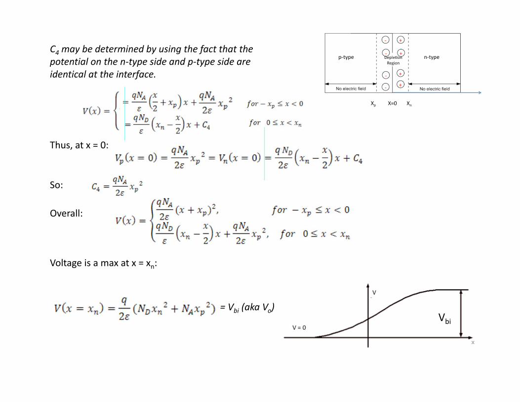
C4 may be determined by using the fact that the potential on the n-type side and p-type side are identical at the interface.
Thus, at x = 0:
So:
Overall:
Voltage is a max at x = xn:
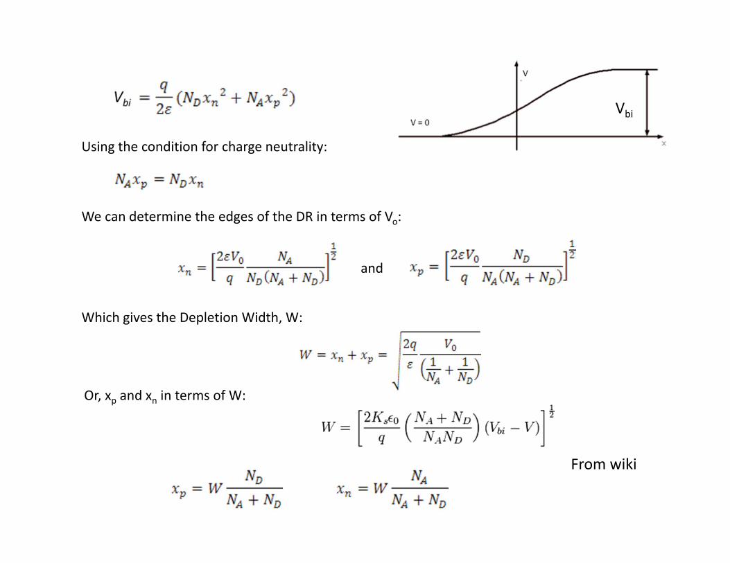
Vbi
= Vbi (aka Vo)

H. Föll: http://www.tf.uni-kiel.de/matwis/amat/semi_en/kap_2/backbone/r2_2_4.html
Vo (aka VBI) is the difference between the Fermi Levels in the two contacting “bits”
Electrons in the two bits have different electrochemical potentials (i.e. different Ef’s)
Charge transfer occurs at contact(electron go down from the vacuum level, holes go “up”)
At equilibrium, there is no net transport (Ef is constant throughout the device)
VBI
VBI
Vbi
Using the condition for charge neutrality:
We can determine the edges of the DR in terms of Vo:
and
Which gives the Depletion Width, W:
Or, xp and xn in terms of W:
From wiki