The Operational Amplifier - Electrical engineeringjbornema/ELEC300/300-02 - Op Amp-I.pdf1 The...
39
1 The Operational Amplifier The operational amplifier is a building block of modern electronic instrumentation. Therefore, mastery of operational amplifier fundamentals is paramount to any practical application of electronic circuits. Specialists in electronic instruments find employment in medical schools, hospitals, research laboratories, aircraft industries, and thousands of other industries where electronic instruments are routinely used. The operational amplifier is often called the op amp for short.
Transcript of The Operational Amplifier - Electrical engineeringjbornema/ELEC300/300-02 - Op Amp-I.pdf1 The...

1
The Operational Amplifier The operational amplifier is a building block of modern electronic
instrumentation.
Therefore, mastery of operational amplifier fundamentals is paramount to any practical application of electronic circuits.
Specialists in electronic instruments find employment in medical schools, hospitals, research laboratories, aircraft industries, and thousands of other industries where electronic instruments are routinely used.
The operational amplifier is often called the op amp for short.

2
Op Amp The op amp is an electronic device consisting of a complex
arrangement of resistors, transistors, capacitors, and diodes. A full discussion of what is inside the op amp is the subject of another course.
In this course, it will suffice to treat the op amp as a circuit building block and simply study what takes place at its terminals.
3
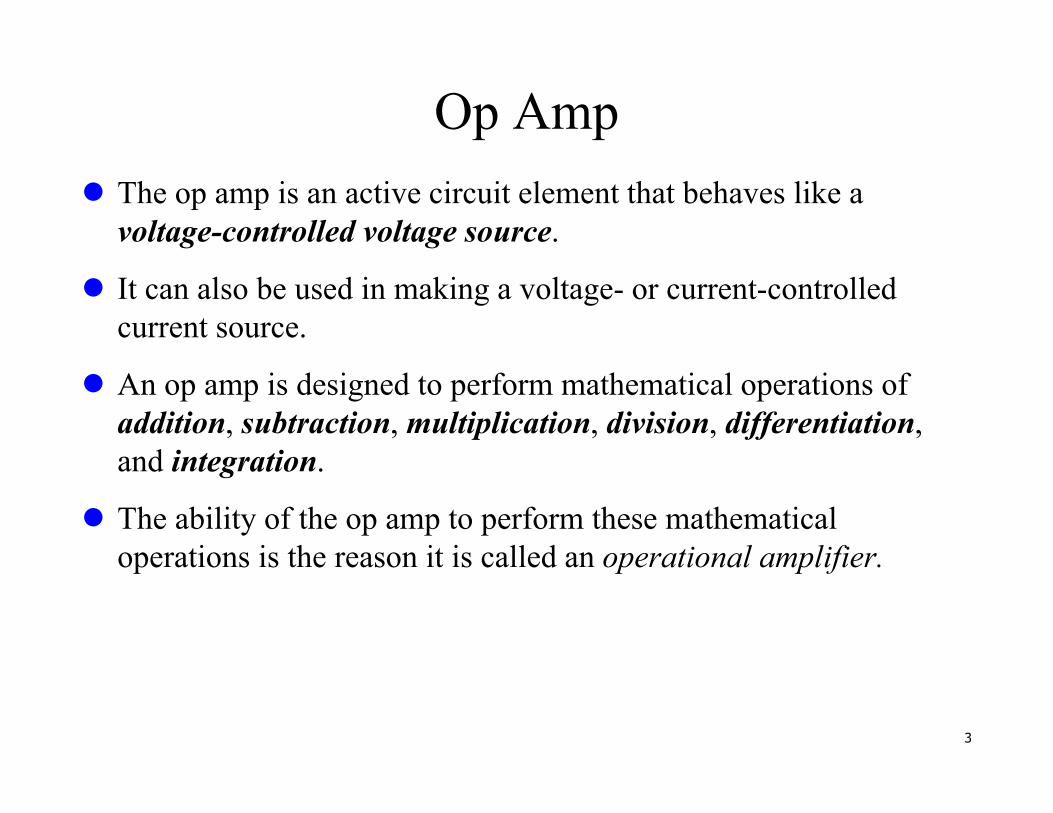
Op Amp The op amp is an active circuit element that behaves like a
voltage-controlled voltage source.
It can also be used in making a voltage- or current-controlled current source.
An op amp is designed to perform mathematical operations of addition, subtraction, multiplication, division, differentiation, and integration.
The ability of the op amp to perform these mathematical operations is the reason it is called an operational amplifier.

4
Op Amp Pin Configuration Op amps are commercially available in integrated circuit packages
in several forms. The figure shows a typical op amp package.
The eight-lead Dual Inline Package (DIP) of an op amp.

5A typical op amp: pin configuration and circuit symbol.
Op Amp Circuit Symbol

6
Powering the Op Amp As an active element, the op amp must be powered by a voltage
supply. Although the power supplies are often ignored in op amp circuit diagrams for the sake of simplicity, the power supply currents must not be overlooked.
Powering the op amp.
0 0p n c ci i i i i+ -+ + + + =
7
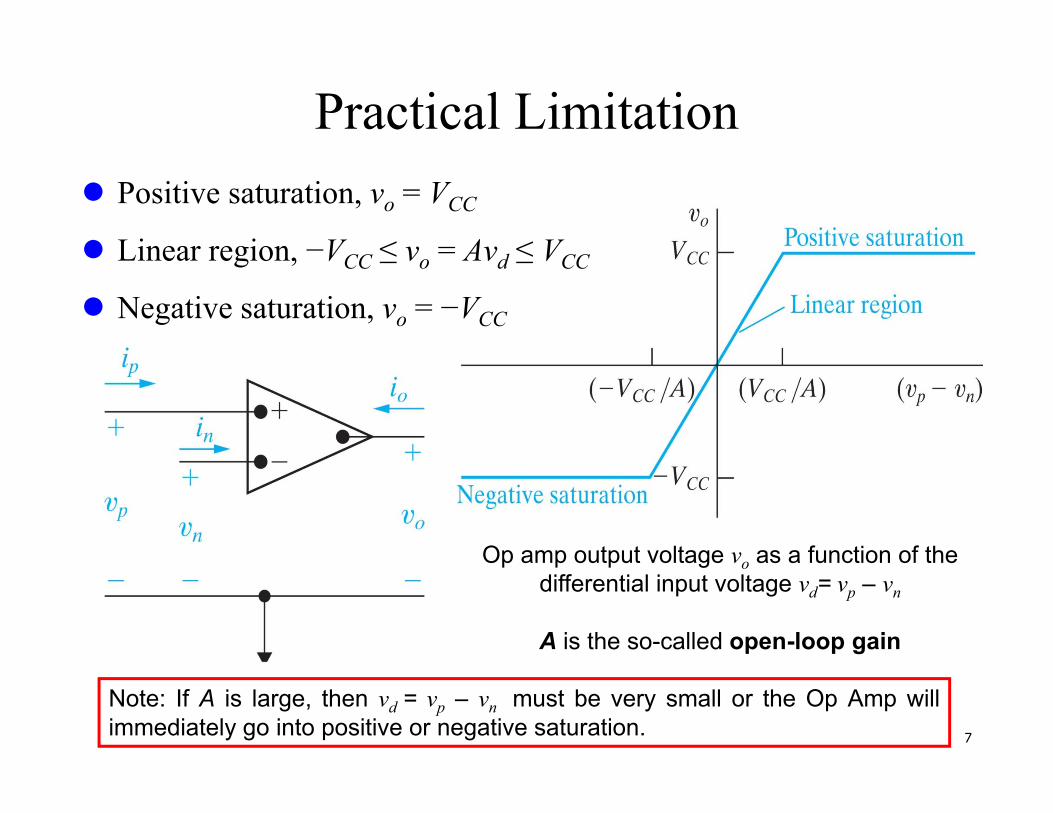
Practical Limitation Positive saturation, vo = VCC
Linear region, −VCC ≤ vo = Avd ≤ VCC
Negative saturation, vo = −VCC
Op amp output voltage vo as a function of the differential input voltage vd= vp – vn
A is the so-called open-loop gain
Note: If A is large, then vd = vp – vn must be very small or the Op Amp willimmediately go into positive or negative saturation.

8
Op Amp Equivalent Circuit The input resistance Ri is
the Thevenin equivalent resistance seen at the input terminals
The output resistance Ro is the Thevenin equivalent resistance seen at the output
Equivalent circuit of the non-ideal op amp.

9
Open Loop Gain The differential input voltage vd is given by vd= vp – vn
The op amp senses the difference between the two inputs, multiplies it by the gain A, and causes the resulting voltage to appear at the output. Thus, the output vo is given by
A is called the open-loop voltage gain because it is the gain of the op amp without any external feedback from output to input.
How to stabilize an amplifier with a very large gain ?
vo= Avd = A(vp – vn)

10
Closed Loop Gain The concept of feedback is crucial to our understanding of op amp
circuits.
A negative feedback is achieved when the output is fed back to the inverting terminal of the op amp.
When there is a feedback path from output to input, the ratio of the output voltage to the input voltage is called the closed-loop gain.
The closed-loop gain is almost insensitive to the open-loop gain A of the op amp.
For this reason, op amps are used in circuits with feedback paths.

11
Negative Feedback
1v+
+
++
+ FFv
iv ovFv
A
Feedback factor FF o
o
vF v F v
v= =
1
Open loop gain
Closed loop gain
o
i
o
vA
vv
Kv
=
=
1Closed loop gain
1 1o o o i
F i F i i i o i
v v v v A AKv v v v v v v Fv v FA
= = = = =+ + + +
1 11
K if A FF A F
= »+
5Assume a passive feedback network with 1, then 10 andF A F£ =
1 1KF
= ³

12
Ideal Op Amp An op amp is ideal if it has the following characteristics:
1. Infinite open-loop gain, A ≈ ∞2. Infinite input resistance, Ri ≈ ∞3. Zero output resistance, Ro ≈ 0
The currents into both input terminals are zero The voltage across the input terminals is negligibly small
Ideal op amp model
0ȴ
= - » i
d p n
Rv v v
0, 0p n
p n
i i
v v
= =
=

13
Inverting Amplifier
An inverting amplifier reverses the polarity of the input signal while amplifying it.
0
But 0 for an ideal op amp
n s f
s n o n
s f
n p
s o
s f
fo s
s
i i i
v v v vR R
v v
v vR R
Rv v
R
= =-
- -=-
= =
=-
=-
fo
s s
Rvv R
=-The voltage gain Av is

10V
-15V
80k
16k
14
Example 5.1Assume that the op amp is ideal. Calculate the output voltage vo for the following values of vs : 0.4V, 2.0V, 3.5V, -0.6V, -1.6V, -2.4V.

15
Example 1Find the output voltage of the op amp circuit. Calculate the current through the feedback resistor.
i

16
Example 2Determine vo.
0
0
0
6V40k 20k
12V 23 12V
- -=
- = -
= -
a a
a a
a
v v v
v v vv v
0
2V
6V 12V 6V
= =
= - =-
a bv v
v

17
Example 5.2a) Design an inverting amplifier with a voltage gain of -12. Use 15V power supplies.b) What range of input voltages allows the op amp to operate in its linear region?
15V
-15V
a) Since ,
choose 1k 12k
fo s
s
s f
Rv v
RR R
=-
= =
( )( )b) 15V 12
15V 12 1.25V
³ -
£ =s
s
v
v

18
Noninverting Amplifier
An noninverting amplifier provides a positive gain which is greater or equal unity.
Since 0
Use voltage divider to get :
1
p p g n
n
sn o g
f s
f s fo g g
s s
i v v v
vRv v v
R R
R R Rv v v
R R
= = =
= =+
æ ö+ ÷ç ÷ = = +ç ÷ç ÷çè ø
1 fo
g s
Rvv R
= +The voltage gain Av is
The series resistance for vg is often omitted. Why is it useful in practice?

19
Voltage Follower
The voltage follower.
Such a circuit has a very high input impedance and is therefore useful as anintermediate-stage (or buffer) amplifier to isolate one circuit from another. Thevoltage follower minimizes interaction between the two stages and eliminates interstage loading.
A voltage follower used to isolate two cascaded stages of a circuit.
1
0,
fo i
s
f s
Rv v
RR R
æ ö÷ç ÷= +ç ÷ç ÷çè ø
= ¥ o iv v=
20
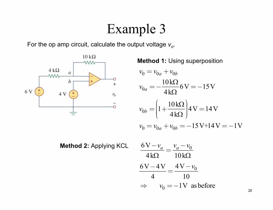
Example 3For the op amp circuit, calculate the output voltage vo.
Method 1: Using superposition
Method 2: Applying KCL
0 0 0
0
0
0 0 0
10k 6V 15V4k
10k1 4V 14V4k
15V+14V 1V
= +
=- =-
æ ö÷ç ÷= + =ç ÷ç ÷çè ø
= + =- =-
a b
a
b
a b
v v v
v
v
v v v
0
0
0
6V4k 10k
4V6V 4V4 10
1V as before
- -=
--=
=-
a av v v
v
v

21
Example 4
Calculate vo.
v1
By voltage division:
18k 3V 2V
8k 4k= =
+v
0 15k12k
3.5 2V 7V
æ ö÷ç ÷= +ç ÷ç ÷çè ø
= ⋅ =
v v
Noninverting amplifier:
22
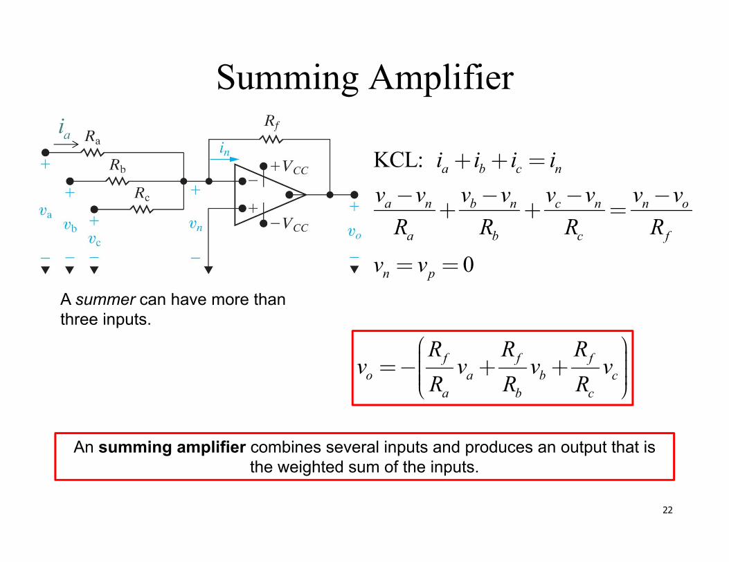
Summing Amplifier
A summer can have more than three inputs.
An summing amplifier combines several inputs and produces an output that is the weighted sum of the inputs.
KCL:
0
a b c n
a n b n c n n o
a b c f
n p
i i i iv v v v v v v v
R R R R
v v
+ + =
- - - -+ + =
= =
ai
f f fo a b c
a b c
R R Rv v v v
R R R
æ ö÷ç ÷=- + +ç ÷ç ÷çè ø

23
Example 5Find vo and io.
08 8 81.5V+ 2V 1.2V 3.8V20 10 6
æ ö÷ç=- =-÷ç ÷÷çè øv
0 00
3.8V 3.8V 1.425mA8k 4k 8k 4k
- -= + = + =-
v vi

24
Digital-to-Analog ConverterFour-bit DAC:(a) block diagram(b) binary weighted ladder type

25
Example 6In the op amp circuit, let Rf = 10 kΩ, R1 = 10 kΩ, R2 = 20 kΩ, R3 = 40 kΩ, and R4 = 80 kΩ. Obtain the analog output for binary inputs [0000], [0001], [0010], . . . , [1111].

26
Difference Amplifier
A difference amplifier amplifies the difference between two inputs but rejects any signals common to the two inputs.
0b a an
a b
R v R vv
R R+
=+
n pv v=
( )0
0
Note: If
If and
a c bb a
b d a
a b c d b a
R R Rv v v
R R RR R R R v v v
= = -
= = = -
0
0( )
a n n o
a b
b a b n a n a
a b n b a a
v v v vR R
R v R v R v R vR R v R v R v
- -=
- = -
+ = +
dp b
c d
Rv v
R R=
+
( )( )
d a b bo b a
a c d a
R R R Rv v v
R R R R+
= -+

27
Example 7Design an op amp circuit with inputs v1 and v2 such that vo = −5v1+3v2.
4 1 2 22 1
1 3 4 1
( )( )o
R R R Rv v v
R R R R+
= -+
2 1 2 22 1
1 3 4 1
(1 )(1 )o
R R R Rv v v
R R R R+
= -+
Design 1

28
Example 7 cont’dDesign a different op amp circuit with inputs v1 and v2 such that vo = −5v1+3v2.
Design 2

29
Example 8Design a difference amplifier with gain of 4.
Figure 5.24
( )31 20 2 1
2 4 1if = = -
RR Rv v v
R R R
2 1 2 22 1
1 3 4 1
(1 )(1 )o
R R R Rv v v
R R R R+
= -+
22 1
1
Since the gain is 4,
4 4= =R
R RR
314 3
2 4
But
4= =RR
R RR R

30
Show that:
An instrumentation amplifier is an amplifier of low-level signals used in process control or measurement applications and is commercially available in single-package units.
Instrumentation Amplifier
31
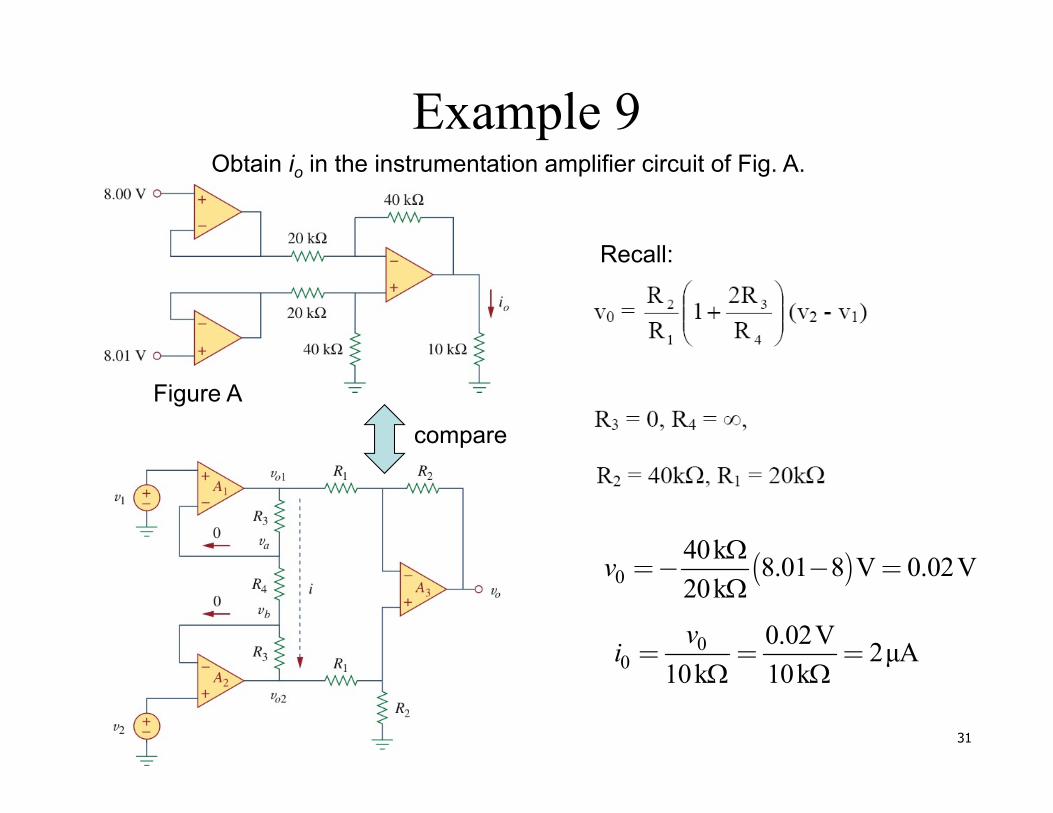
Example 9Obtain io in the instrumentation amplifier circuit of Fig. A.
Recall:
Figure A
compare
( )040k 8.01 8 V 0.02V20k
=- - =v
00
0.02V 2μA10k 10k
= = =v
i

32
Summary

33
Summary

34
Op Amp Circuit Analysis With PSPICE PSpice does not have a model for an ideal op amp.
PSpice has four nonideal, commercially available op amps in its eval.slblibrary.
Note that each of them requires dc supplies, without which the op amp will not work.
Nonideal op amp models available in PSpice.

35
Example 10Use PSpice to solve for vo / vs.
3.9983V 1.999152V
o
s
vv
-= =-
20kUsing the ideal op-amp model: 2.010k
=- =-o
s
vv

36
Controlled Sources Voltage Controlled Voltage Source (VCVS)
Non-inverting amplifier:
2
11 independent ofo
Li
v RR
v R= +

37
Controlled Sources Voltage Controlled Current Source (VCCS)
Redraw the circuit:
2
2 2
o
o
Rv v v vR R
v v
+ -= = =+
=
22KCL: 0 0
2
1 independent of
i o oi o o
i o o o io
o i L
v v v vi i i i
R Rv v v v v
iR R R R R
i v RR
- -+ - = + - =
= - + - =
=
38
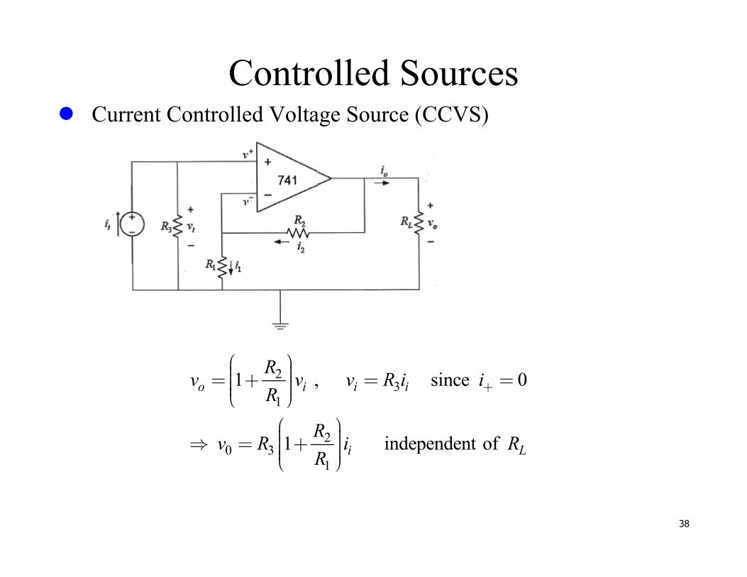
Controlled Sources Current Controlled Voltage Source (CCVS)
23
1
20 3
1
1 , since 0
1 independent of
o i i i
i L
Rv v v R i i
R
Rv R i R
R
+
æ ö÷ç ÷= + = =ç ÷ç ÷çè øæ ö÷ç ÷ = +ç ÷ç ÷çè ø

39
Controlled Sources Current Controlled Current Source (CCCS)
1 1 2 2
12 1 1 2
2
1
2
KVL: 0 , 0
, ,
independent of
D D
i o
o i L
R i v R i vR
i i i i i iRR
i i RR
- - = =
= = =
=
Redraw the circuit: