The Modular Multilevel Converter for High Step-Up Ratio...
12
IEEE TRANSACTIONS ON INDUSTRIAL ELECTRONICS, VOL. 62, NO. 8, AUGUST 2015 4925 The Modular Multilevel Converter for High Step-Up Ratio DC–DC Conversion Xiaotian Zhang, Member, IEEE , and Timothy C. Green, Senior Member, IEEE Abstract —High step-up ratio dc–dc converters with megawatt ratings are of interest in wind turbine inter- faces and high-voltage direct-current systems. This paper presents a modular multilevel dc–dc converter based on the standard boost converter topology but with the normal single switches replaced by a number of capacitor-clamped submodules. The converter is operated in resonant mode with resonance between submodule capacitors and the arm inductor. A phase-shifted switching arrangement is applied such that there is a constant number, i.e., N , of sub- modules supporting the high voltage at a time. In this oper- ation mode, the step-up ratio is dependent on the number of submodules and the inductor charging ratio. The converter exhibits scalability without using a transformer and is ca- pable of bidirectional power flow. An application example of a wind turbine interface with a 10 : 1 conversion ratio is demonstrated in simulation. The experimental verification of the concept using a lab-scale prototype is provided. Index Terms—DC transformer, high-voltage direct cur- rent (HVDC) converters, modular multilevel converters (MMCs), resonant conversion, step-up dc–dc conversion. I. I NTRODUCTION M ULTILEVEL converters used for medium-voltage and high-voltage applications significantly reduce the har- monic content of the output voltage as compared with the traditional two-level converters [1]–[4]. Multilevel converter schemes for dc–dc conversion are becoming popular [5] in renewable energy applications following the success of this approach in dc–ac conversion. There are many different types of multilevel converters developed [6], which can be directly or indirectly used as step-up dc–dc converters. The modular multilevel converter (MMC) is found to have more attractive features than the others. Diode-clamped converters have a large number of diodes required, and with the unbalancing issue, making the system impractical to implement. Conventional fly- ing capacitor converters [7] require many capacitors connected in series. The total series capacitance is much smaller than that of a single one. Therefore, the total volume of capaci- tors required is quite high. Generalized multilevel converters can be used for step-up dc–dc conversion [8], [9], but the Manuscript received May 27, 2014; revised September 22, 2014 and November 19, 2014; accepted December 27, 2014. Date of publication January 19, 2015; date of current version June 26, 2015. This work was supported by the Engineering and Physical Sciences Research Council, U.K., under Grant EP/K006312/1. The authors are with the Department of Electrical Engineering, Imperial College London, London, SW7 2AZ, U.K. (e-mail: xiaotian. [email protected]; [email protected]). Color versions of one or more of the figures in this paper are available online at http://ieeexplore.ieee.org. Digital Object Identifier 10.1109/TIE.2015.2393846 topology results in a large size when the step ratio is high. Other topologies such as input-parallel output-series (IPOS) converters [10] and switched capacitor converters have been proposed and developed for step-up dc–dc conversion [11]– [13]. The IPOS converters use resonant submodules to achieve high-power conversion and efficiency [14], but the main dis- advantage is the requirement of a large number of isolation transformers, which have high potential differences between the windings. Switched capacitor converters with series-parallel topologies are subject to incremental voltage stress either on the module switch or on the module capacitor. The highest voltage stress is close to the output (high-side) dc voltage. The switched capacitor converters are also subject to high charge losses and overshoot currents. This problem can be mitigated by driving metal–oxide–semiconductor field-effect transistors (MOSFETs) with very high switching frequency. Therefore, switched capacitor converters are only used under a low-voltage condition. A power-electronics-based Cockcroft–Walton multi- plier has been demonstrated in [15]. This is a light and cheap solution for high-voltage dc experiments when only unidirec- tional step-up conversion is required. A bidirectional medium- voltage “ladder”-shaped dc–dc converter is proposed in [16], which can achieve a high step ratio. The advantage is that the converter does not require synchronization of switching between submodules. However, the current ratings in different submodules are not the same, and the inductor currents close to the low-voltage side are high. In medium- and high-voltage applications, MMCs used for dc–dc conversion are emerging technologies [5], [17]. These converters are based on conventional MMCs [18]–[20]. MMCs usually require a complicated balancing control scheme to maintain the voltage levels. However, they provide more than two levels and good waveform quality. Cells with fault can also be bypassed while keeping the system operational. High modularity and redundancy are the main advantages of MMCs. Until now, there has been no direct and simple solution for large step-up ratio dc–dc conversion using the MMC approach. This paper presents a new topology and control scheme of a modular multilevel bidirectional dc–dc converter with high step-up ratio. It is based on the conventional boost converter with groups of submodules placed in both the diode and switch positions. The proposed converter can achieve a high step ratio. Phase-shifted pulsewidth modulation (PWM) is used to achieve a high effective operating frequency for a given submodule switching frequency. The proposed converter is bidirectional and suitable for low-power dc–dc applications as it has the feature of modularity, simplicity, and flexibility. The configura- tion of the circuit and its operation principle are presented and verified by experimental results from a downscaled prototype. 0278-0046 © 2015 IEEE. Personal use is permitted, but republication/redistribution requires IEEE permission. See http://www.ieee.org/publications_standards/publications/rights/index.html for more information.
Transcript of The Modular Multilevel Converter for High Step-Up Ratio...

IEEE TRANSACTIONS ON INDUSTRIAL ELECTRONICS, VOL. 62, NO. 8, AUGUST 2015 4925
The Modular Multilevel Converter for HighStep-Up Ratio DC–DC Conversion
Xiaotian Zhang, Member, IEEE , and Timothy C. Green, Senior Member, IEEE
Abstract—High step-up ratio dc–dc converters withmegawatt ratings are of interest in wind turbine inter-faces and high-voltage direct-current systems. This paperpresents a modular multilevel dc–dc converter based onthe standard boost converter topology but with the normalsingle switches replaced by a number of capacitor-clampedsubmodules. The converter is operated in resonant modewith resonance between submodule capacitors and the arminductor. A phase-shifted switching arrangement is appliedsuch that there is a constant number, i.e., N , of sub-modules supporting the high voltage at a time. In this oper-ation mode, the step-up ratio is dependent on the number ofsubmodules and the inductor charging ratio. The converterexhibits scalability without using a transformer and is ca-pable of bidirectional power flow. An application exampleof a wind turbine interface with a 10 : 1 conversion ratio isdemonstrated in simulation. The experimental verificationof the concept using a lab-scale prototype is provided.
Index Terms—DC transformer, high-voltage direct cur-rent (HVDC) converters, modular multilevel converters(MMCs), resonant conversion, step-up dc–dc conversion.
I. INTRODUCTION
MULTILEVEL converters used for medium-voltage andhigh-voltage applications significantly reduce the har-
monic content of the output voltage as compared with thetraditional two-level converters [1]–[4]. Multilevel converterschemes for dc–dc conversion are becoming popular [5] inrenewable energy applications following the success of thisapproach in dc–ac conversion. There are many different typesof multilevel converters developed [6], which can be directlyor indirectly used as step-up dc–dc converters. The modularmultilevel converter (MMC) is found to have more attractivefeatures than the others. Diode-clamped converters have a largenumber of diodes required, and with the unbalancing issue,making the system impractical to implement. Conventional fly-ing capacitor converters [7] require many capacitors connectedin series. The total series capacitance is much smaller thanthat of a single one. Therefore, the total volume of capaci-tors required is quite high. Generalized multilevel converterscan be used for step-up dc–dc conversion [8], [9], but the
Manuscript received May 27, 2014; revised September 22, 2014 andNovember 19, 2014; accepted December 27, 2014. Date of publicationJanuary 19, 2015; date of current version June 26, 2015. This work wassupported by the Engineering and Physical Sciences Research Council,U.K., under Grant EP/K006312/1.
The authors are with the Department of Electrical Engineering,Imperial College London, London, SW7 2AZ, U.K. (e-mail: [email protected]; [email protected]).
Color versions of one or more of the figures in this paper are availableonline at http://ieeexplore.ieee.org.
Digital Object Identifier 10.1109/TIE.2015.2393846
topology results in a large size when the step ratio is high.Other topologies such as input-parallel output-series (IPOS)converters [10] and switched capacitor converters have beenproposed and developed for step-up dc–dc conversion [11]–[13]. The IPOS converters use resonant submodules to achievehigh-power conversion and efficiency [14], but the main dis-advantage is the requirement of a large number of isolationtransformers, which have high potential differences betweenthe windings. Switched capacitor converters with series-paralleltopologies are subject to incremental voltage stress either onthe module switch or on the module capacitor. The highestvoltage stress is close to the output (high-side) dc voltage. Theswitched capacitor converters are also subject to high chargelosses and overshoot currents. This problem can be mitigatedby driving metal–oxide–semiconductor field-effect transistors(MOSFETs) with very high switching frequency. Therefore,switched capacitor converters are only used under a low-voltagecondition. A power-electronics-based Cockcroft–Walton multi-plier has been demonstrated in [15]. This is a light and cheapsolution for high-voltage dc experiments when only unidirec-tional step-up conversion is required. A bidirectional medium-voltage “ladder”-shaped dc–dc converter is proposed in [16],which can achieve a high step ratio. The advantage is thatthe converter does not require synchronization of switchingbetween submodules. However, the current ratings in differentsubmodules are not the same, and the inductor currents close tothe low-voltage side are high.
In medium- and high-voltage applications, MMCs used fordc–dc conversion are emerging technologies [5], [17]. Theseconverters are based on conventional MMCs [18]–[20]. MMCsusually require a complicated balancing control scheme tomaintain the voltage levels. However, they provide more thantwo levels and good waveform quality. Cells with fault canalso be bypassed while keeping the system operational. Highmodularity and redundancy are the main advantages of MMCs.
Until now, there has been no direct and simple solution forlarge step-up ratio dc–dc conversion using the MMC approach.This paper presents a new topology and control scheme ofa modular multilevel bidirectional dc–dc converter with highstep-up ratio. It is based on the conventional boost converterwith groups of submodules placed in both the diode and switchpositions. The proposed converter can achieve a high step ratio.Phase-shifted pulsewidth modulation (PWM) is used to achievea high effective operating frequency for a given submoduleswitching frequency. The proposed converter is bidirectionaland suitable for low-power dc–dc applications as it has thefeature of modularity, simplicity, and flexibility. The configura-tion of the circuit and its operation principle are presented andverified by experimental results from a downscaled prototype.
0278-0046 © 2015 IEEE. Personal use is permitted, but republication/redistribution requires IEEE permission.See http://www.ieee.org/publications_standards/publications/rights/index.html for more information.

4926 IEEE TRANSACTIONS ON INDUSTRIAL ELECTRONICS, VOL. 62, NO. 8, AUGUST 2015
Fig. 1. Single switches and submodules with active clamping.
Fig. 2. Bidirectional dc–dc converters. (a) Conventional two-leveldc–dc converter. (b) Novel modular multilevel dc–dc converter.
II. BIDIRECTIONAL MODULAR MULTILEVEL
DC–DC CONVERTERS
In converting a simple standard switched-mode circuit toa modular multilevel format, a variety of capacitor-clampedsubmodules are required. Fig. 1 shows clamped single switchesthat use the half-bridge configuration in which replacements fora single insulated-gate bipolar transistor (IGBT), a diode, andan IGBT with an antiparallel diode are illustrated. The abilityto clamp the off-state voltage across a switch when a stackof switches is connected in series is crucial in forming MMCtopologies. Using this idea, the modular multilevel invertertopology was generated by clamping the series-connectedIGBTs in the conventional two-level inverter. With activeclamping, each switch has a well-defined voltage and goodsharing between submodules.
The active-clamping idea can also be applied to dc–dcconverters. The upper IGBT in the half bridge is termed asclamping IGBT, whereas the lower IGBT is termed as clampedIGBT. The classic bidirectional two-level dc–dc converter isshown in Fig. 2(a). It consists of an inductor on the low-voltageside, two IGBTs with antiparallel diodes, and capacitors on bothinput and output sides. Replacing all the switches by series-connected submodules with active clamping, the bidirectionalbuck–boost converter becomes the modular multilevel dc–dcconverter shown in Fig. 2(b). The number of upper submodulesis not required to be the same as the number of the lower sub-modules; however, special operation techniques are required.
III. HIGH STEP-UP RATIO MODULAR MULTILEVEL
DC–DC CONVERTER
This section describes the operation method for the proposeddc–dc converter. The analysis focuses on step-up dc–dc conver-sion. To simplify the analysis, the theoretical developments arebased on the following assumptions.
1) The switches are ideal, and the submodules are identical.
Fig. 3. Unidirectional step-up dc–dc converters. (a) Conventional boostconverter. (b) Proposed modular multilevel step-up dc–dc converter.
2) The converter is lossless.3) In steady state, the capacitor dc voltages are balanced.
A. System Configuration
The configuration of the step-up conversion is provided todemonstrate the concept. The most commonly used boost con-verter topology with a single IGBT and a single diode is shownin Fig. 3(a). The IGBT in the lower position is used for chargingthe input inductor L. The diode in the upper position of thecircuit is automatically commutated on when the inductor isdischarging current to the high-voltage capacitor CH . Applyingactive clamping (see Fig. 1) to the two switches, the modularmultilevel unidirectional step-up converter with two stacks ofsubmodules is obtained as shown in Fig. 3(b). The numberof the half-bridge (clamped IGBT) submodules in the lowerposition is M . The number of the chopper (clamped diode)submodules in the upper position is N . The output (high-side)voltage is approximately equal to the sum of capacitor voltagesof the stack of submodules once duty cycles are accountedfor. There will be small differences between the instantaneousvoltage across the stack (as submodules switch) and the voltageacross CH , and this is accommodated by including the smallinductor LS . A large capacitor CL would normally be present atthe input (low voltage) side. The step-down conversion is con-figured using the similar concept. The circuit of the proposedconverter for step-down operation is shown in Fig. 4.
B. Phase-Shift Control
The proposed converter has various operating modes result-ing in different operating features and step-up ratios. Apartfrom the high step-up ratio operation mode, which is the focusof this paper, the converter can also be used for high step-down ratio dc–dc conversion providing power for an auxiliaryelectronic circuit in medium-voltage systems. Moreover, withsimilar numbers of submodules in the upper stack and thelower stack, the converter can also be used for low-step-ratiohigh-voltage dc–dc conversion. Phase-shifted PWM is usedto control the modular multilevel step-up dc–dc converter.

ZHANG AND GREEN: MODULAR MULTILEVEL CONVERTER FOR HIGH STEP-UP RATIO DC–DC CONVERSION 4927
Fig. 4. Unidirectional step-down dc–dc converters. (a) Conventionalbuck converter. (b) Proposed modular multilevel dc–dc converter.
Phase-shifted PWM is arranged with a high duty cycle suchthat only one submodule capacitor at a time is out of the seriesconnection, and thus, the step-up ratio of the circuit becomesdependent on the number of upper cells N . The effectivefrequency of this excitation is much higher than the frequencyof switching of an individual cell.
To demonstrate the principle of interleaved PWM, a step-up converter with four submodules in the diode position in thecircuit of Fig. 3(b) is considered (N = 4). To ensure that eitherfour or three submodules are injecting voltage at any time, eachmust be operated with a duty cycle above 75%. For illustration,90% is used. One module could be used in the lower positionoperating at four times the switching frequency of the uppermodules (to give the same effective frequency). Instead, thesystem will be illustrated with two submodules in the lower po-sition operating at twice the frequency of the upper submodulesand with interleaved pulses. Assuming the submodule capacitorvoltages to be constant, the key waveforms of the submodulevoltages are shown in Fig. 5.
It can be seen in Fig. 5 that the upper (clamped diode)cells are synchronously switched with the lower (clampedIGBT) cells so that the total voltage of the upper cells vNand lower cells vM are complementary. This guarantees analmost constant dc voltage with a small ripple on the high-voltage side. The equivalent operating frequency is four timesthe switching frequency of the upper cells (fe = 4fs) andis twice the switching frequency of the lower cells. As thefrequency of the ripple on the high-voltage side is high, thepassive components of the output filter do not need to be large.The current waveforms in Fig. 5 will be explained with the step-up operation.
The step-down operation has the same stack voltage wave-forms as that of the step-up conversion. The voltage waveformsof the submodules are not shown. The time-domain waveformsof the stacks are shown in Fig. 6. In the step-down operation, thecurrent directions and waveforms are different from that in thestep-down operation. The operation of step-down conversionwill be analyzed in detail in the following section.
Fig. 5. Time-domain key waveforms of the proposed step-up converter.
Fig. 6. Time-domain key waveforms of the proposed converter withstep-down operation.
C. High Conversion Ratio
The proposed converter is aimed at high step-up ratio dc–dcconversion. The analysis of operation and conversion ratio willproceed by examining one equivalent cycle Te in Fig. 5. Fig. 7shows the detailed circuit diagrams with current paths high-lighted for the two modes of the circuit. Mode 1 starts when theIGBT in Cell 4 is switched on and ends when the IGBT in Cell 1switches off [see Fig. 7(a)]. The IGBT in Cell 1 switches offwhen the lower IGBT in Cell 5 switches off, and this definesthe beginning of Mode 2 [see Fig. 7(b)]. Mode 2 ends whenthe IGBT of Cell 1 is switched on again. Modes 1 and 2 areanalogous to the on- and off-states of the simple boost converterbut with the difference that current can flow in both paths inboth modes. The current flowing through the input inductor,upper cells (clamped diodes), and lower cells (clamped IGBTs)are defined as iL, iN , and iM , respectively.

4928 IEEE TRANSACTIONS ON INDUSTRIAL ELECTRONICS, VOL. 62, NO. 8, AUGUST 2015
Fig. 7. Step-up operation modes in the first equivalent operating cycle. (a) Mode 1. (b) Mode 2.
In Mode 1, the current iL of inductor L is directly chargedby the low-side (input) voltage vL via the IGBTs in Cell 5 andCell 6. The capacitors C1, C2, C3, and C4 are in series withthe inductor Ls and the high-side (output) capacitor CH , andtogether, they form a resonant tank. Because CH is large and thecell capacitors are smaller and placed in series, the resonanceis dominated by the cell capacitors, and CH can be ignored.Therefore, the resonant frequency is
fr =1
2π√LsC/N
. (1)
In the case of N = 4, fr = 1/π√LsC. When the converter
enters Mode 2 from Mode 1, capacitor C5 is connected intothe circuit, whereas capacitor C1 is out of series connection.The capacitors C2, C3, C4, and C5 are in resonant tank withLs and CH . As the inductor L is relatively large, the current iLis considered as from a current source. Therefore, the resonantfrequency in Mode 2 is also dependent on four series-connectedcapacitors and the series inductor Ls. When the lower (clampedIGBT) cells and the upper (clamped diode) cells use the samecapacitors, the resonant frequency in Mode 2 is the same as thatin Mode 1.
In Fig. 7(b), it can be seen that the current iN cannot benegative in Mode 2 because one cell (Cell 1 in the figure) isacting as a diode. If the actual resonant frequency is slightly
higher than fe, by the end of Mode 2, the current iN reacheszero, and the circuit operates in discontinuous conductionmode (DCM).
When Mode 1 begins, the current iL is directly charged bythe low-side voltage source. Meanwhile, the current iN startsto resonate (starting from zero) with the frequency of fr. Thecurrent iM is iL minus iN . When the circuit enters Mode 2from Mode 1, since vC5 is higher than vL, the inductor currentiL reduces. As the circuit operates in DCM, before the endof the equivalent operating cycle, the current iN falls to zero,and the current iM is equal to iL until a new cycle begins. Thesimulation result later in this paper will illustrate this.
To obtain the voltage conversion ratio, the charging ratio d isdefined as the time duration of Mode 1 relative to the period,i.e., Te of the equivalent operating cycle. In steady state, theincrease and decrease of iL over a equivalent cycle Te shouldbe the same; hence,
vLTed
L=
(vCj − vL)Te(1− d)
L(2)
with j = 5 or j = 6. The capacitor voltages of the lowersubmodules can be written as
vCj =vL
1− d. (3)

ZHANG AND GREEN: MODULAR MULTILEVEL CONVERTER FOR HIGH STEP-UP RATIO DC–DC CONVERSION 4929
The sum of average stack voltages vN and vM should be equalto the high-side voltage, i.e., vH , which yields
vH =N − 1 + d
N
N∑
j=1
vCj +1− d
M
N+M∑
j=N+1
vCj . (4)
Under ideal conditions, the capacitor voltages are balanced andequal to vC . The voltage conversion ratio can be derived bysubstituting (3) into (4), i.e.,
vHvL
=N
1− d. (5)
It can be seen that without increasing d, the conversion ratio canbe increased by using higher numbers of upper submodules N .In the case of N = 4, the conversion ratio is vH/vL=4/(1−d).
The current stresses in the converter should be estimated be-cause it is important in determining the power losses and deviceratings. The low-side (input) inductor current iL comprises a dccomponent and a sawtooth-shaped ripple. The average currentof iL can be derived from the power consumed on the high-voltage side. Here, it is assumed that the load dc current is Io.Therefore,
IL =vHvL
Io. (6)
The peak-to-peak ripple ΔIL can be obtained from the chargingtime of inductor L, i.e.,
ΔIL =vLTed
L. (7)
The current stress on the clamped-diode (upper) stack de-pends on iN . The dc component of iN goes on to feed theload, and its ac component circulates within the resonant tank.It will be assumed that the ac component of iN is approximatelysinusoidal with a root mean square (RMS) value of IN1 at theresonant frequency. The power transferred out of the clamped-diode (upper) stack by the flow of the dc current is
P1 = (N − 1 + d)vCIo. (8)
On the other hand, the ac voltage of the upper stack is a squarewave with a peak-to-peak value of vC . Therefore, the RMSvalue of this square wave is vC/2. The power transferred intothe stack by the sinusoidal resonant current interacting with thesquare-wave component of the stack voltage is
P2 =vC2IN1λ (9)
with λ as the power factor for this voltage and current combina-tion. The value of λ can be obtained from numerical solutions.The maximum, i.e., λ = 1, is achieved when the charging ratiois d = 0.5. If the converter is lossless, the dc power and acpower of the upper stack should be equal. Therefore
IN1 =N − 1 + d
λIo. (10)
After iL and iN are estimated, the current stress on the lowerstack can be determined by iM = iL − iN . A rough estimationof |iM | < |iL|+ |iN | can also be used.
Although the converter is proposed for high step-up ratiodc–dc conversion, it also has the capability of step-down dc–dcconversion. Fig. 8 shows the detailed circuit diagrams with cur-rent paths highlighted for the two modes of the circuit. Mode 1starts when the clamped IGBT in Cell 1 is switched on andends when the clamped IGBT in Cell 1 is switched off [seeFig. 8(a)]. When the clamped IGBT in Cell 1 switches off andthe clamping IGBT in Cell 5 switches off, the converter beginsto enter Mode 2 [see Fig. 8(b)]. Mode 2 ends when the clampingIGBT of Cell 6 is switched off. For operation analysis, thecurrent directions are defined opposite to the current directionsin the step-up operation.
As the voltage on the inductor L in Mode 1 is higher than thatin Mode 2, the current iL of inductor L is charged in Mode 1and discharged in Mode 2. During Mode 1, the inductor Ls
and the capacitors C2, C3, and C4 are charged, and therefore,the clamped diodes in the lower cells are reverse-biased. Thereis no current flowing through the lower stack. If the capacitorvoltages are assumed to be constant, the currents iL and iNshould linearly increase in Mode 1 and iL equals iN . Theslight increase in the cell capacitor voltages does not affect thewave shapes obviously. When the converter enters Mode 2 fromMode 1, all the cell capacitors in the upper stack are in serieswith the inductor Ls. The inductor L starts to linearly discharge,and the clamped diode in Cell 6 is commutated. Meanwhile,the capacitors C1, C2, C3, and C4 in series with the inductorLs form a resonant tank to discharge the energy stored in thepassive components from Mode 1. The resonant frequency frin the step-down operation is the same as that in the step-upoperation. Therefore, the current iM flowing through the lowerstack can be written as
iM = iL − iN . (11)
This analysis for step-down operation explains the currentwaveforms in Fig. 6. The inductor current has a sawtooth waveshape, and the lower stack current is zero during Mode 1.In Mode 1, the upper stack current is equal to the inductorcurrent. In Mode 2, the upper stack current is discharging with aresonant wave shape, which, together with the inductor current,determines the lower stack current. To derive the step-downoutput voltage vL as a function of charging ratio d (defined instep-up operation) and high voltage vH , the inductor current iLis assumed to be the same after one equivalent charging cycle.Similar to the step-up operation, it can be approximated thatNvCj = vH . The conversion ratio can be derived as
vHvL
=N
1− d. (12)
The step-down operation has the same step ratio function as thatin the step-up operation. This means that the proposed modularmultilevel dc–dc converter is similar to the conventional bidi-rectional dc–dc converter in terms of step ratio. By changing thecurrent directions, the converter achieves bidirectional power

4930 IEEE TRANSACTIONS ON INDUSTRIAL ELECTRONICS, VOL. 62, NO. 8, AUGUST 2015
Fig. 8. Step-down operation modes in the first equivalent operating cycle. (a) Mode 1. (b) Mode 2.
conversion and the same step ratio without modifying theswitching arrangement.
D. Capacitor Voltage Clamping Mechanism
The converter has a cell capacitor voltage clamping mech-anism. This property can be explained by using the step-up operation for example. As is shown in Fig. 7(a), whenthe low-voltage-side inductor is charging (Mode 1), there arecapacitors of Cell 1, Cell 2, Cell 3, and Cell 4 supportingthe high-side dc voltage. Since the resonant tank formed bythe cell capacitors and inductor Ls has an impedance closeto zero at the resonant frequency, the ac voltage drop acrossthe resonant components is negligible. Therefore, the outputhigh voltage is almost equal to vo = vC1 + vC2 + vC3 + vC4.In the next operation mode [see Fig. 7(b)], the output voltagecan be expressed as vo = vC2 + vC3 + vC4 + vC5. Hence, bycomparing the two equations, it can be stated that vC1 = vC5.In the next operating cycle, using the same method, one canstate that vC2 = vC6. The following operation mode sequencein the remaining switching cycle gives vC1 = vC3 = vC5 andvC2 = vC4 = vC6. The capacitor voltages of the upper cells arealways clamped by the capacitor voltages of the lower cells.Therefore, by balancing the two lower cell capacitors, the dcvoltages of all the capacitors should be equal in steady state.For the converter with only one cell in the lower position, the
Fig. 9. Half-bridge cell voltage controller.
circuit will have inherent balancing ability and does not evenrequire additional balancing control. When needed, balancingcontrol for lower cells can be used as shown in Fig. 9.
The reference cell voltage is calculated by averaging thecapacitor voltages in half-bridge cells, i.e.,
v∗ref =1
M
N+M∑
j=N+1
v∗Cj (13)
with v∗Cj as the sampled capacitor voltage. As capacitor volt-ages contain considerable ac components, first-order lowpassfilters are used. By comparing the reference voltage with the dcvoltage of each cell, a proportional feedback control is used forregulation. A dead zone is created to allow a small toleranceof voltage imbalance. A saturation function is used to limit theadjustable range. As the current at the switching instant, andin average is positive while the cell capacitor is connected inseries to the others, this capacitor voltage can be charged byincreasing the cell duty cycle.

ZHANG AND GREEN: MODULAR MULTILEVEL CONVERTER FOR HIGH STEP-UP RATIO DC–DC CONVERSION 4931
Fig. 10. General control for output voltage.
TABLE IPARAMETERS OF THE APPLICATION EXAMPLE
The general output voltage feedback control for all submod-ules is shown in Fig. 10. The voltage regulator is represented byHv(z), usually an antiwindup proportional-integral controlleror a phase lead controller. The gain in this controller forsubmodules in the lower position is doubled compared with thatin the upper position because of the duty-cycle differences (seeFig. 5). The pulse generated by the lower submodules is almostcomplementary to that of upper submodules.
IV. STEP-UP CONVERTER APPLICATION EXAMPLE
The proposed converter can be used as a dc transformer withhigh step-up ratio. One interesting application of the proposedconverter is to convert a low-voltage 400-V source into distri-bution voltage level (a few kilovolts). The converter can furtherbe reconfigured with a transformer to provide isolation betweeninput and output. This can boost the dc voltage with a veryhigh step-up ratio and enables direct conversion from a windturbine dc-link to a high-voltage direct current (HVDC) link forexample. Due to the page limit, an isolated step-up converter isnot considered further here.
The application example discussed here is based on theproposed MMC dc–dc converter with two lower submodules(one redundant) and four upper submodules. It operates as astep-up converter from 3 to 30 kV. The application is a turbineconverter delivering 1-MW power to a 30-kV medium-voltagedc collection bus. Series-connected ABB HiPak IGBT modulesof type 5SNA 1200G450300 are used as the main switches. Theparameters of this example are listed in Table I.
The simulation results of the step-up converter in the appli-cation example are shown in Fig. 11. The typical voltage dropacross the IGBT is lower than 4 V, which is much smaller thanthe maximum switch voltage of 4.5 kV. In this example, theeffect of the voltage drop can be considered negligible. Theoutput voltage is a dc voltage with a ripple lower than 1%. Asthe converter is operating in resonant mode, the loss calculationis very complicated. According to IEC 61803, the losses mea-sured in the HVDC converter are not likely to be a sufficientaccurate indication of actual losses. Therefore, IEC 61803standardizes a method of calculating the power losses. Inadditional to IEC 61803, the draft IEC 62751 breaks downpower losses into individual components [21]. The power losses
Fig. 11. Simulated currents and output voltage of the converter.(X-axis: Time, 50 μs/div; Y-axis: magnitude of current, 500 A/div;magnitude of voltage, 10 kV/div).
of the proposed converter have been calculated based on thesimulation results.
The switching losses are comprised of the upper-stackIGBT switching losses P sw
N1, upper-stack diode reverse recoverylosses P sw
N2, lower-stack IGBT switching losses P swM1 and P sw
M2.The clamping IGBTs in the upper stack are soft switchedunder a zero-current condition. The total energy loss whenclamping IGBTs turn off is a function of the current iN at thatswitching instant and so is written as Eoff(iN ). Therefore, theupper-stack clamping IGBTs’ switching losses are calculated asP swN1 = 2NfsEoff(iN ). The clamped diodes in the upper stack
are soft switched off so that the reverse recovery losses arenegligible. The clamping IGBTs in the lower stack are softswitched on and off. However, their antiparallel diodes havereverse recovery losses as P sw
M1 = 4MfsErr(iM ). The clampedIGBTs in the lower stack are hard switched on and off withthe losses written as P sw
M2 = 4MfsEoff(iM ) + 4MfsEon(iM ).The total switching losses are
P swtot = 2NfsEoff(iN ) + 4MfsErr(iM )
+ 4MfsEoff(iM ) + 4MfsEon(iM ). (14)
The switching losses are obtained as P swtot = 35.2 kW. The
conduction losses comprise the upper-stack IGBT conductionlosses P con
N1 , upper-stack diode conduction losses P conN2 , lower-
stack IGBT conduction losses P conM1 , and lower-stack diode con-
duction losses P conM2 . The saturation voltage VCE and forward
voltage VF are functions of the current, which can be foundfrom the datasheet. The conduction losses of the upper-stackIGBTs and diodes are given by P con
N1 = 2NINVCE(IN )λN1
and P conN2 = 2NINVF(IN )λN2, respectively. The factor λ rep-
resents the ratio of the conduction time to the switching period.The conduction losses of the lower stack are written as P con
M1 =2MIMVCE(IM )λM1 and P con
M2 = 2MIMVF(IM )λM2. The to-tal conduction losses are
P contot = 2NINVCE(IN )λN1 + 2NINVF(IN )λN2
+2MIMVCE(IM )λM1 + 2MIMVF(IM )λM2. (15)
Summarizing the numerical result of the conduction losscalculation yields P con
tot = 7.7 kW. The resistive losses mainly

4932 IEEE TRANSACTIONS ON INDUSTRIAL ELECTRONICS, VOL. 62, NO. 8, AUGUST 2015
TABLE IIEFFICIENCY VERSUS INPUT VOLTAGE
come from the losses in the input inductor and the resonantinductor, represented by P res
L = I2LrL and P resLs
= I2NrLs, re-
spectively. The total resistive losses are
P restot = P res
L + P resLs
. (16)
The calculated resistive losses are P restot = 21.9 kW. The total
losses are calculated as
P losstot = P sw
tot + P contot + P res
tot . (17)
The total power losses are calculated as P losstot = 64.8 kW. By
comparing the ratio between power losses and output power,the efficiency in the application example is about 94%. Asthe switch voltages and currents are high, switching losses aremore than half the total losses. The calculated efficiencies with1-kHz switching frequency is shown in Table II. It can be seenthat with voltage level increase, the efficiency is improved.Further improvement of efficiency could be achieved withfewer redundant submodules and reduced switching frequency.However, the cost would increase due to larger volume capaci-tors required.
The main disadvantage of a nonisolated dc–dc converteris the high current peak in the high-voltage side. A similardrawback exists in a conventional boost converter where theswitch needs to withstand the high peak voltage and should beable to conduct the highest peak current. However, the proposedconverter has a modular structure that is scalable in terms ofvoltage levels and avoids the difficulty of voltage sharing in aseries connection of a large number of IGBTs. The equivalentswitching frequency of the proposed converter is much higherthan that of a standard boost converter while maintaining lowswitching frequency in each module. Moreover, it eliminatesthe use of bulky isolation transformers where entire high volt-age applies on the insulation between windings. This convertermay not suit all step-up applications, but where the voltage ratiois in the region of 10 : 1, the advantages of this converter mayprove useful. In practice, a specific tradeoff should be madefor the chosen application so that the converter can be properlyconfigured.
V. EXPERIMENTAL RESULTS
A downscaled experimental prototype with four upper cellsand two lower cells was constructed based on the proposedcircuit in Fig. 2(b) for verification. The submodules wereimplemented using capacitors with a nominal capacitance valueof 50 μF. As a result, the resonant frequency was expected tobe approximately 4.1 kHz. The switching frequencies for uppercells and lower cells were fixed as 1 and 2 kHz, respectively,giving an effective operational frequency of 4 kHz, which isslightly less than the resonant frequency. The complete circuitparameters are listed in Table III.
TABLE IIIPARAMETERS OF THE EXPERIMENTAL SYSTEM
A. Open-Loop Tests
The open-loop tests used a fixed charging ratio of d = 0.6.For the step-up operation, the input voltage was 30 V, andthe output voltage was expected to be 300 V. However, as theswitches are not ideal, the high voltage will be lower than theexpected value. For comparison purposes, the converter usingthe experimental parameters has been simulated. Fig. 12(a) and(b) shows the waveforms of simulated currents and voltageswith voltage drop in each switch set to 1 V. The experimentalcurrent and voltage waveforms shown in Fig. 12(c) and (d) arequite similar to the corresponding simulation results. However,when the current iN in Mode 1 cross zero from negative, thecurrent resonance is dramatically damped compared with thesimulation result in Fig. 11 (the application example) wherethis current is freely resonating. This is caused by the voltagedrop across the switches (which appears relatively large inthis downscaled prototype). When the current iN is negativein Mode 1, the voltage drop across the diodes is positivecompared with vN . When the current iN changes to positive,the voltage drop across the IGBTs becomes negative comparedwith vN . Because in this mode the inductor L is chargingand the capacitor CH is discharging, the rise of current iN issuppressed until the end of this mode. When Mode 2 begins,the inductor current iL is discharged to the high-voltage side,and the current iN keeps resonating until it reaches zero or theend of the equivalent operating cycle.
The simulated stack voltage waveforms in Fig. 12(b) areclose to the experimentally measured stack voltage waveformsin Fig. 12(d). However, the upper-stack voltage vN is lower thanthe expected amplitude. The sum of the lower-stack voltageand upper-stack voltage is far below 300 V. As a result, theconversion ratio is lower than 10:1. The output voltage shouldbe adjusted by closed-loop control to achieve the required level.
For step-down operation, the input high voltage was set to300 V. The output low voltage is expected to be 30 V. However,as there are voltage drops in the real switches, the output voltagemay be lower than expected. Fig. 13(a) and (b) shows thesimulated step-down current and voltage waveforms with 1-Vvoltage drop in each switch. In contrast, the experimental step-down current and voltage waveforms in Fig. 13(c) and (d) arequite similar to the relevant simulation results. The inductor Lis charging in Mode 1 and discharging in Mode 2. The lower-stack current is zero during this mode. The currents iL and iNshould linearly increase in Mode 1 and iL equals iN . In Mode 2,

ZHANG AND GREEN: MODULAR MULTILEVEL CONVERTER FOR HIGH STEP-UP RATIO DC–DC CONVERSION 4933
Fig. 12. Simulation and experimental waveforms of the proposed converter for step-up conversion (X-axis: time, 50 μs/div). (a) Simulated currents(Y-axis: magnitude of current, 2 A/div). (b) Simulated voltages (Y-axis: magnitude of voltage, 100 V/div). (c) Experimental currents (Y-axis: magnitudeof current, 2 A/div). (d) Experimental voltages (Y-axis: magnitude of voltage, 100 V/div).
Fig. 13. Simulation and experimental waveforms of the proposed converter for step-down conversion (X-axis: time, 50 μs/div). (a) Simulatedcurrents (Y-axis: magnitude of current, 2 A/div). (b) Simulated voltages (Y-axis: magnitude of voltage, 100 V/div). (c) Experimental currents (Y-axis:magnitude of current, 2 A/div). (d) Experimental voltages (Y-axis: magnitude of voltage, 100 V/div).
the current iL starts to linearly decrease. All the cell capacitorsin the upper stack are in series with the inductor Ls, forming aresonant tank for iN to discharge. The stack voltage waveformsare in accordance with the waveforms in Fig. 6. This verifiesthe operation analysis of the proposed converter. The outputhigh voltage is around 25 V with vH = 300 V under open-loopcontrol. The output voltage is lower than the expected value dueto the voltage drop across the IGBTs.
The current and voltage waveforms of submodules in step-up operation are shown in Fig. 14. As Cell 1 can represent allthe upper cells and Cell 6 can represent the lower cells, thewaveforms of Cell 1 and Cell 6 are shown. It can be seen inFig. 14(a) that the resonant current frequency is 4 kHz and theswitching frequency of upper cells is 1 kHz. As explained inthe previous sections, the interleaved PWM can quadruple theequivalent operating frequency. The switch-on and switch-off
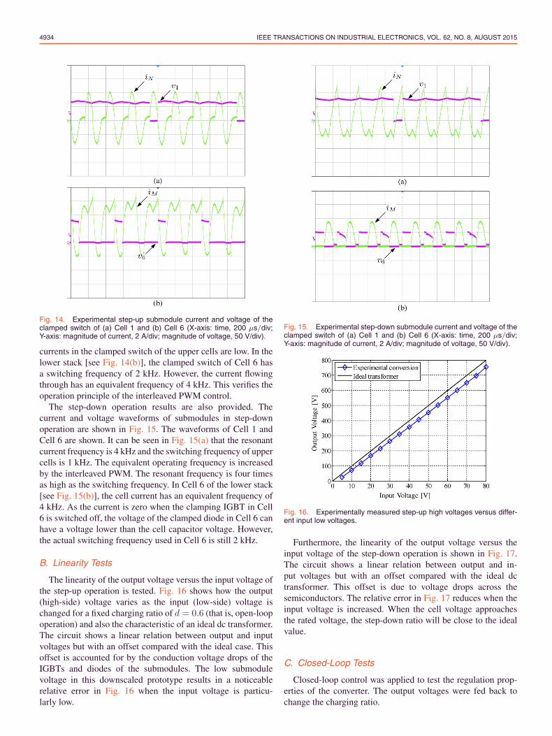
4934 IEEE TRANSACTIONS ON INDUSTRIAL ELECTRONICS, VOL. 62, NO. 8, AUGUST 2015
Fig. 14. Experimental step-up submodule current and voltage of theclamped switch of (a) Cell 1 and (b) Cell 6 (X-axis: time, 200 μs/div;Y-axis: magnitude of current, 2 A/div; magnitude of voltage, 50 V/div).
currents in the clamped switch of the upper cells are low. In thelower stack [see Fig. 14(b)], the clamped switch of Cell 6 hasa switching frequency of 2 kHz. However, the current flowingthrough has an equivalent frequency of 4 kHz. This verifies theoperation principle of the interleaved PWM control.
The step-down operation results are also provided. Thecurrent and voltage waveforms of submodules in step-downoperation are shown in Fig. 15. The waveforms of Cell 1 andCell 6 are shown. It can be seen in Fig. 15(a) that the resonantcurrent frequency is 4 kHz and the switching frequency of uppercells is 1 kHz. The equivalent operating frequency is increasedby the interleaved PWM. The resonant frequency is four timesas high as the switching frequency. In Cell 6 of the lower stack[see Fig. 15(b)], the cell current has an equivalent frequency of4 kHz. As the current is zero when the clamping IGBT in Cell6 is switched off, the voltage of the clamped diode in Cell 6 canhave a voltage lower than the cell capacitor voltage. However,the actual switching frequency used in Cell 6 is still 2 kHz.
B. Linearity Tests
The linearity of the output voltage versus the input voltage ofthe step-up operation is tested. Fig. 16 shows how the output(high-side) voltage varies as the input (low-side) voltage ischanged for a fixed charging ratio of d = 0.6 (that is, open-loopoperation) and also the characteristic of an ideal dc transformer.The circuit shows a linear relation between output and inputvoltages but with an offset compared with the ideal case. Thisoffset is accounted for by the conduction voltage drops of theIGBTs and diodes of the submodules. The low submodulevoltage in this downscaled prototype results in a noticeablerelative error in Fig. 16 when the input voltage is particu-larly low.
Fig. 15. Experimental step-down submodule current and voltage of theclamped switch of (a) Cell 1 and (b) Cell 6 (X-axis: time, 200 μs/div;Y-axis: magnitude of current, 2 A/div; magnitude of voltage, 50 V/div).
Fig. 16. Experimentally measured step-up high voltages versus differ-ent input low voltages.
Furthermore, the linearity of the output voltage versus theinput voltage of the step-down operation is shown in Fig. 17.The circuit shows a linear relation between output and in-put voltages but with an offset compared with the ideal dctransformer. This offset is due to voltage drops across thesemiconductors. The relative error in Fig. 17 reduces when theinput voltage is increased. When the cell voltage approachesthe rated voltage, the step-down ratio will be close to the idealvalue.
C. Closed-Loop Tests
Closed-loop control was applied to test the regulation prop-erties of the converter. The output voltages were fed back tochange the charging ratio.
ZHANG AND GREEN: MODULAR MULTILEVEL CONVERTER FOR HIGH STEP-UP RATIO DC–DC CONVERSION 4935
Fig. 17. Experimentally measured step-down low voltages versus dif-ferent input high voltages.
Fig. 18. Experimental waveforms of the closed-loop control step-up conversion (X-axis: Time, 50 μs/div). (a) Experimental currents(Y-axis: magnitude of current, 2 A/div). (b) Experimental voltages (Y-axis:magnitude of voltage, 100 V/div).
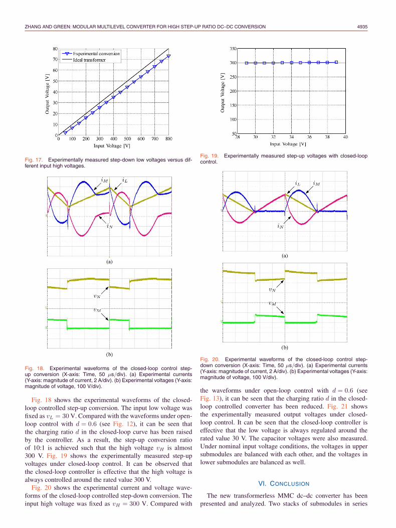
Fig. 18 shows the experimental waveforms of the closed-loop controlled step-up conversion. The input low voltage wasfixed as vL = 30 V. Compared with the waveforms under open-loop control with d = 0.6 (see Fig. 12), it can be seen thatthe charging ratio d in the closed-loop curve has been raisedby the controller. As a result, the step-up conversion ratioof 10:1 is achieved such that the high voltage vH is almost300 V. Fig. 19 shows the experimentally measured step-upvoltages under closed-loop control. It can be observed thatthe closed-loop controller is effective that the high voltage isalways controlled around the rated value 300 V.
Fig. 20 shows the experimental current and voltage wave-forms of the closed-loop controlled step-down conversion. Theinput high voltage was fixed as vH = 300 V. Compared with
Fig. 19. Experimentally measured step-up voltages with closed-loopcontrol.
Fig. 20. Experimental waveforms of the closed-loop control step-down conversion (X-axis: Time, 50 μs/div). (a) Experimental currents(Y-axis: magnitude of current, 2 A/div). (b) Experimental voltages (Y-axis:magnitude of voltage, 100 V/div).
the waveforms under open-loop control with d = 0.6 (seeFig. 13), it can be seen that the charging ratio d in the closed-loop controlled converter has been reduced. Fig. 21 showsthe experimentally measured output voltages under closed-loop control. It can be seen that the closed-loop controller iseffective that the low voltage is always regulated around therated value 30 V. The capacitor voltages were also measured.Under nominal input voltage conditions, the voltages in uppersubmodules are balanced with each other, and the voltages inlower submodules are balanced as well.
VI. CONCLUSION
The new transformerless MMC dc–dc converter has beenpresented and analyzed. Two stacks of submodules in series

4936 IEEE TRANSACTIONS ON INDUSTRIAL ELECTRONICS, VOL. 62, NO. 8, AUGUST 2015
Fig. 21. Experimentally measured step-down voltages with closed-loop control.
arrangement support the high voltage. The dc capacitors of thesubmodules are used also for resonant operation. The proposedconverter has a bidirectional conversion ability. The step-upoperation and the step-down operation are demonstrated. Thisconverter is capable of operating under open-loop control as adc transformer with good linearity. Alternatively, closed-loopcontrol can be applied for trimming of the output voltage. Theoperating principle was verified through a bench-scale exper-imental prototype. The proposed converter may exhibit rela-tively high losses because of the high ac current that resonatesin the submodules, but reasonably high efficiency was shownto be possible in high-voltage applications. Further efficiencyimprovement can be achieved with lower switching frequency,but cell capacitors with a higher volume will be required. Theconverter can achieve a large step-up conversion ratio withoutthe use of transformers. The proposed converter has the featuresof modularity, scalability, and simplicity, and these may makeit attractive in some special applications.
REFERENCES
[1] S. Kouro et al., “Recent advances and industrial applications of multilevelconverters,” IEEE Trans. Ind. Electron., vol. 57, no. 8, pp. 2553–2580,Aug. 2010.
[2] J. I. Leon et al., “Multidimensional modulation technique for cascadedmultilevel converters,” IEEE Trans. Ind. Electron., vol. 58, no. 2, pp. 412–420, Feb. 2011.
[3] M. A. Perez, J. Rodriguez, E. J. Fuentes, and F. Kammerer, “Predic-tive control of ac–ac modular multilevel converters,” IEEE Trans. Ind.Electron., vol. 59, no. 7, pp. 2832–2839, Jul. 2012.
[4] E. Solas et al., “Modular multilevel converter with different submoduleconcepts—Part II: Experimental validation and comparison for HVDCapplication,” IEEE Trans. Ind. Electron., vol. 60, no. 10, pp. 4536–4545,Oct. 2013.
[5] J. Ferreira, “The multilevel modular dc converter,” IEEE Trans. PowerElectron., vol. 28, no. 10, pp. 4460–4465, Oct. 2013.
[6] M. Perez, S. Bernet, J. Rodriguez, S. Kouro, and R. Lizana, “Circuittopologies, modelling, control schemes and applications of modular mul-tilevel converters,” IEEE Trans. Power Electron., vol. 30, no. 1, pp. 4–17,Jan. 2015.
[7] T. A. Meynard and H. Foch, “Multi-level conversion: High voltage chop-pers and voltage-source inverters,” in Proc. IEEE Power Electron. Spec.Conf., 1992, pp. 397–403.
[8] F. Z. Peng, “A generalized multilevel inverter topology with self volt-age balancing,” IEEE Trans. Ind. Appl., vol. 37, no. 2, pp. 611–618,Mar./Apr. 2001.
[9] S. Busquets-Monge, S. Alepuz, and J. Bordonau, “A bidirectional multi-level boost–buck dc–dc converter,” IEEE Trans. Power Electron., vol. 26,no. 8, pp. 2172–2183, Aug. 2011.
[10] T. Todorcevic, P. Bauer, J. A. Ferreira, and R. van Kessel, “Bidirectionalmodular multilevel dc–dc converter control and efficiency improvementsthrough separate module control method,” in Proc. IEEE Energy Convers.Congr. Expo., 2013, pp. 2038–2043.
[11] K. D. T. Ngo and R. Webster, “Steady-state analysis and design of aswitched-capacitor dc–dc converter,” IEEE Trans. Aerop. Electron. Syst.,vol. 30, no. 1, pp. 92–101, Jan. 1994.
[12] F. Khan and L. Tolbert, “A multilevel modular capacitor-clamped DC–DCconverter,” IEEE Trans. Ind. Appl., vol. 43, no. 6, pp. 1628–1638,Nov./Dec. 2007.
[13] D. Cao and F. Z. Peng, “Zero-current-switching multilevel modularswitched-capacitor DC–DC converter,” IEEE Trans. Ind. Appl., vol. 46,no. 6, pp. 2536–2544, Nov./Dec. 2010.
[14] G. Ortiz, H. Uemura, D. Bortis, J. W. Kolar, and O. Apeldoorn, “Modelingof soft-switching losses of IGBTs in high-power high-efficiency dual-active-bridge dc/dc converters,” IEEE Trans. Electron Devices, vol. 60,no. 2, pp. 587–597, Feb. 2013.
[15] C.-M. Young, M.-H. Chen, T.-A. Chang, C.-C. Ko, and K.-K. Jen, “Cas-cade Cockcroft–Walton voltage multiplier applied to transformerless highstep-up dc–dc converter,” IEEE Trans. Ind. Electron., vol. 60, no. 2,pp. 523–537, Feb. 2013.
[16] M. Kasper, D. Bortis, and J. W. Kolar, “Novel high voltage conversionratio rainstick dc/dc converters,” in Proc. IEEE Energy Convers. Congr.Expo., 2013, pp. 789–796.
[17] X. Zhang, T. C. Green, and A. Junyent-Ferre, “A new resonant modu-lar multilevel step-down dc–dc converter with inherent-balancing,” IEEETrans. Power Electron., vol. 30, no. 1, pp. 78–88, Jan. 2015.
[18] T. Luth, M. M. C. Merlin, T. C. Green, F. Hassan, and C. D. Barker, “High-frequency operation of a dc/ac/dc system for HVDC applications,” IEEETrans. Power Electron., vol. 29, no. 8, pp. 4107–4115, Aug. 2014.
[19] S. Allebrod, R. Hamerski, and R. Marquardt, “New transformerless, scal-able modular multilevel converters for HVDC-transmission,” in Proc.IEEE PESC, 2008, pp. 174–179.
[20] A. Antonopoulos, L. Angquist, L. Harnefors, K. Ilves, and H.-P. Nee,“Global asymptotic stability of modular multilevel converters,” IEEETrans. Ind. Electron., vol. 61, no. 2, pp. 603–612, Feb. 2014.
[21] P. S. Jones and C. C. Davidson, “Calculation of power losses for MMC-based VSC HVDC stations,” in Proc. EPE, 2013, pp. 1–10.
Xiaotian Zhang (S’11–M’12) was born in Xi’an,China, in 1983. He received the B.S. (with hon-ors) and M.S. degrees in electrical engineeringfrom Jiaotong University, Xi’an, in 2006 and2009, respectively, and the Ph.D. degree (withhonors) in electrical engineering and electronicsfrom the University of Liverpool, Liverpool, U.K.,in 2012.
Since 2013, he has been with the Depart-ment of Electrical Engineering, Imperial CollegeLondon, London, U.K. His research interests
include control modeling and circuit design of multilevel converters forhigh-voltage applications.
Timothy C. Green (M’89–SM’02) received theB.Sc. degree (first-class honors) in electri-cal engineering from Imperial College London,London, U.K., in 1986 and the Ph.D. degree inelectrical engineering from Heriot-Watt Univer-sity, Edinburgh, U.K., in 1990.
He was a Lecturer with Heriot-Watt Universityuntil 1994 and is currently a Professor of elec-trical power engineering with Imperial CollegeLondon, the Deputy Head of the Electrical andElectronic Engineering Department, and the Di-
rector of the Energy Futures Laboratory. His research interest is informulating the future from the electricity network to support low-carbonfutures. A particular theme is how the flexibility of power electronics andcontrol can be used to accommodate new-generation patterns and newforms of load, such as EV charging, as part of the emerging smart grid.He has particular interest in offshore dc networks and the managementof low-voltage networks. He leads the HubNet consortium of eight U.K.universities coordinating research in low-carbon energy networks and isthe Network Champion for the Research Councils U.K.
Dr. Green is a Chartered Engineer in the U.K.