The MINOS Light Injection Calibration System - arxiv.org · The MINOS Light Injection Calibration...
28
arXiv:hep-ex/0204021v1 17 Apr 2002 The MINOS Light Injection Calibration System P. Adamson a,1 J. Alner b B. Anderson c T. Chase d P.J. Dervan c,2 T. Durkin b E. Falk a P.G. Harris a,* D.G. Michael e R. Morse a R. Nichol c R. Saakyan c C. Smith c P.N. Smith a J. Thomas c R. Webb f R.F. White a a Department of Physics, University of Sussex, Falmer, Brighton BN1 9QJ, UK b Rutherford Appleton Laboratory, Chilton, Didcot OX11 0QX, UK c Department of Physics, University College London, Gower Street, London WC1E 6BT, UK d Mechanical Engineering Department, University of Minnesota, 111 Church St SE, Minneapolis MN 55455, USA e California Institute of Technology High Energy Physics, Charles C. Lauritsen Laboratory, Pasadena CA 91125, USA f Texas A & M University Physics Department, College Station, TX 77843-4242 Abstract A description is given of the light-injection calibration system that has been de- veloped for the MINOS long-baseline neutrino oscillation experiment. The system is based upon pulsed blue LEDs monitored by PIN photodiodes. It is designed to measure non-linearities in the PMT gain curves, as well as monitoring any drifts in PMT gain, at the 1% level. Key words: Light injection, calibration, LED, PMT, MINOS PACS: 29.40.Vj, 29.40.Mc * Corresponding author. Email address: [email protected] (P.G. Harris). 1 Present address: Department of Physics, University College London, Gower Street, London WC1E 6BT, UK 2 Present address: Department of Physics & Astronomy, Hicks Building, University of Sheffield, Hounsfield Road, Sheffield S3 7RH, UK Preprint submitted to Elsevier Science 5 February 2008
Transcript of The MINOS Light Injection Calibration System - arxiv.org · The MINOS Light Injection Calibration...
arX
iv:h
ep-e
x/02
0402
1v1
17
Apr
200
2
The MINOS Light Injection Calibration
System
P. Adamson a,1 J. Alner b B. Anderson c T. Chase d
P.J. Dervan c,2 T. Durkin b E. Falk a P.G. Harris a,∗
D.G. Michael e R. Morse a R. Nichol c R. Saakyan c C. Smith c
P.N. Smith a J. Thomas c R. Webb f R.F. White a
aDepartment of Physics, University of Sussex, Falmer, Brighton BN1 9QJ, UK
bRutherford Appleton Laboratory, Chilton, Didcot OX11 0QX, UK
cDepartment of Physics, University College London, Gower Street, London WC1E
6BT, UK
dMechanical Engineering Department, University of Minnesota, 111 Church St
SE, Minneapolis MN 55455, USA
eCalifornia Institute of Technology High Energy Physics, Charles C. Lauritsen
Laboratory, Pasadena CA 91125, USA
fTexas A & M University Physics Department, College Station, TX 77843-4242
Abstract
A description is given of the light-injection calibration system that has been de-veloped for the MINOS long-baseline neutrino oscillation experiment. The systemis based upon pulsed blue LEDs monitored by PIN photodiodes. It is designed tomeasure non-linearities in the PMT gain curves, as well as monitoring any drifts inPMT gain, at the 1% level.
Key words: Light injection, calibration, LED, PMT, MINOSPACS: 29.40.Vj, 29.40.Mc
∗ Corresponding author.Email address: [email protected] (P.G. Harris).
1 Present address: Department of Physics, University College London, GowerStreet, London WC1E 6BT, UK2 Present address: Department of Physics & Astronomy, Hicks Building, Universityof Sheffield, Hounsfield Road, Sheffield S3 7RH, UK
Preprint submitted to Elsevier Science 5 February 2008

1 MINOS overview
The MINOS experiment [1] will investigate the phenomenon of neutrino oscil-lations [2–4] by sending a beam of muon neutrinos 735 km through the Earthfrom the Fermi National Accelerator Laboratory (FNAL), near Chicago, to adetector in the Soudan Underground Mine State Park in northern Minnesota.The experiment uses three detectors:
(1) The Near Detector (ND) at FNAL. This will determine the character-istics of the neutrino beam before it begins its journey. Only neutrinoevents and cosmic ray muons are measured here; there is no “test beam”available.
(2) The Far Detector (FD), situated 713 m underground in the Soudan mine,where the neutrino beam emerges from the Earth. Like the near detector,this measures only neutrino events and cosmic ray muons.
(3) The Calibration Detector (CD) at CERN is a small detector, similar instructure to both near and far detectors, that is being exposed to particlebeams at CERN to study its response to electrons, muons and hadronsof known energies.
2 MINOS detectors
The MINOS far detector is an 8 m wide octagonal tracking calorimeter, con-sisting of 486 layers of one-inch-thick steel interleaved with scintillator, givinga total mass of 5.4 kilotons. It has a toroidal magnetic field of strength ap-proximately 1.3 T.
Each plane of scintillator consists of 192 strips, each 4 cm wide and 1 cmthick with a co-extruded TiO2 cladding to maximise internal reflection. Lightfrom these strips is wavelength-shifted from blue to green and carried withinacrylic fibres [5] to Hamamatsu [6] multi-anode photomultiplier tubes situatedaround the edge of the detector. Scintillator strips are in orthogonal direc-tions in alternate planes. This gives a 3D readout with an energy resolutionσ/E of approximately 23%/
√E for electromagnetic showers and 55%/
√E for
hadronic showers. The magnetic field allows measurement of the muon mo-mentum by curvature (14% resolution for a 10 GeV muon) as well as by rangefor stopping muons (giving approximately 6% resolution).
2

2.1 Calorimeter energy calibration
In order to measure the neutrino mixing parameters ∆m2 and sin2(2θ) pre-cisely, the energy response of the detectors has to be calibrated to within afew percent. The goal is a 5% absolute measurement of the energy in eachdetector, and consistency to within 2% between the near and far detectors.This is carried out in several stages [7]:
• A light-injection calibration system is required to monitor, and to compen-sate for, changes in amplification (and non-linearity) of the photomultipliertubes used in the detectors. The light-injection system is the principal sub-ject of this paper.
• Cosmic-ray muons are used to perform the strip-to-strip calibration withineach detector, and the relative calibration between the near and far detec-tors [8,9]. The strip-to-strip calibrations do not require a high statisticalprecision (∼ 10% per strip per month), as both muon tracks and hadronicshowers contain many strips. There are expected to be about 530 cosmic rayhits/strip/month in the far detector, giving an accuracy of 2.4% per stripper month, and about 25,000 hits/strip/month in the near detector, givingan accuracy there of 0.3%/strip/month.
Stopping muons can be used to provide the relative calibration of nearto far detectors. There are estimated to be 700 stopping muons per dayin the far detector, and two orders of magnitude more than this in thenear detector. This yields a 1% statistical precision for the near-far detectorcalibration each day.
• A study to compare the energy deposition by muons with that from hadronsand hadronic showers is being carried out with the calibration detector ina charged-particle test beam at CERN.
2.2 Optical readout
The MINOS readout chain is illustrated schematically in Fig. 1. A 1.2 mmKuraray Y11 wavelength-shifting fibre [5] lies in a groove along the length ofeach scintillator strip. Between 16 and 28 such strips are enclosed in a light-tight aluminium case, known as a module. There are eight modules in a fullplane.
The wavelength-shifting fibres run to a connector at the end of the aluminiumcase. Clear fibres [10] then carry the light to boxes containing Hamamatsumulti-anode photomultiplier tubes.
For the far detector, Hamamatsu M16 photomultipliers [11] are used (seeFig. 2), with fibres from eight separate scintillator strips feeding each PMT
3

Front EndElectronics
DAQ
chargedparticle
PMT
Fig. 1. Signal readout path from scintillator to electronics in MINOS. The greenacrylic wavelength-shifting fibre lies within a groove running down the centre of thescintillator strip. Light is carried within this fibre to the edge of the detector, andthen via clear acrylic fibre to the photomultiplier tube.
Fig. 2. The face of a Hamamatsu R5600-M16 multi-anode photomultiplier as usedin the far detector. Photograph courtesy K. Lang.
pixel. This “optical multiplexing”, which provides a substantial saving in thecost of readout electronics, is possible because the event rate at the far detectoris so low that there will never be more than one event in the detector at anyone time. The typical width of a shower event in MINOS is 50 cm, so the1 m spacing between strips illuminating a single pixel is appropriate. Themultiplexing pattern is slightly different on each side of the detector in orderto aid deconvolution.
The far-detector readout electronics uses a modified version of the Viking VA
4

chip [12] made by IDE AS of Norway [13]. This is an integrated circuit con-taining 32 channels of shaping amplifiers and track-and-hold circuitry. Whentriggered, each channel is digitised in turn. The data are then transferred toVME readout control crates, with single-board computers running the Vx-Works real-time operating system.
Instantaneous event rates in the near detector will be 5 × 10⁵ higher than inthe far detector. The near detector therefore uses QIE [14] electronics, a high-speed, multi-ranging ADC system with no dead time. Its principal differencefrom the far detector electronics is that it divides input signals into 19 nstime buckets, and digitises each separately. These separate digitisations arerecombined during the event-building process. The light-injection calibrationsystem incorporates an external trigger that can be used to produce opticalpulses at different starting positions within the 19 ns time bucket, in orderto investigate any possible systematic differences in response at the bucketboundaries.
The near detector is not optically multiplexed (although its muon spectrome-ter section is electronically multiplexed). It uses Hamamatsu M64 (64-anode)photomultiplier tubes, and has a total of 12,000 readout channels. Unlike thefar detector, only one end of each strip is read out: the other end is termi-nated with a reflector to maximise the detected light. The calibration detectorwill use both near and far detector readout systems, in order to carry out asystematic comparison of the responses of each.
3 Light-injection system overview
The light-injection system is based upon pulsed blue light-emitting diodes(LEDs). A rack-mounted box, known as a “pulser box”, contains a set of 20LEDs, each of which has an optical fan-out allowing it to illuminate multipleindividual fibres. These fibres carry light to a set of optical connectors on theback panel of the pulser box.
From the pulser box, optical fibres carry the light to the outer edges ofthe MINOS detector. A set of highly-reflective cavities situated there – the“light-injection modules” – allows the blue LED light to illuminate the greenwavelength-shifting fibres, thus producing pulses of light that mimic the sig-nals from the scintillator.
The intensity of injected light is monitored by PIN photodiodes that are readout simultaneously with the PMTs.
In the following sections, the requirements of and constraints upon the light-
5

injection system are discussed, after which each component of the system isexamined in detail.
4 Light-injection system requirements
4.1 Aims
The purpose of the light injection system is fourfold:
(1) Mapping the gain curve. The response of the photomultiplier tubes be-comes non-linear at light levels exceeding about 100 photoelectrons [11].The light injection system is designed to be able to characterise the re-sponse of every optical readout channel on a regular basis (up to onceper month in routine operation).
(2) Monitoring short-term gain drifts. The gain of a photomultiplier tube issensitive to small changes in temperature and in applied high voltage. Byinjecting light at a single point on the gain curve on an hourly basis, anyresulting changes in gain can be monitored closely and compensated for.
(3) Evaluating PMT gain. Pulsing at very low light levels allows the acqui-sition of single photoelectron spectra for each channel, from which thegain can easily be calculated.
(4) Confirming optical path integrity. The light injection system provides aquick and thorough check to ensure that no fibres are broken.
4.2 Design constraints
A number of constraints were imposed upon the design of the light injectionsystem:
(1) The amount of light applied to any pixels on a given PMT that areilluminated simultaneously should differ by no more than a factor of two.This helps to avoid excessive non-linearities and possible problems fromcrosstalk when injecting light towards the top end of the dynamic range.It is also useful in reducing the amount of data required in order to coverthe dynamic range for all pixels, as one does not then have dimly andbrightly illuminated pixels that require separate calibration operations atdifferent levels of LED brightness.
(2) The M16s used on the far detector are multiplexed, with eight fibrescarrying light to each pixel. No two fibres on any pixel may be illumi-nated simultaneously. Adjacent pixels should also be avoided if possible,
6

to minimise crosstalk problems.(3) The dynamic range of light injected must range from a fraction of a photo-
electron up to several hundred photoelectrons on all pixels. Furthermore,this dynamic range should be covered with a step size of the order of onephotoelectron.
(4) The relative levels of light injected must be measured by a separate devicehaving a response that is linear to 1%, in order to characterise the non-linear response of the PMTs. PIN photodiodes were selected for thispurpose.
(5) The response of the PIN photodiodes must be stable to within 1% overthe timescale of a month.
(6) The relative arrival times of the optical pulses at each PMT must bestable to within approximately a nanosecond.
5 Light-emitting diodes
5.1 LEDs vs. lasers
Previous experiments needing light-injection calibration of the type requiredfor MINOS have often used scintillator excited by pulsed lasers, with a varietyof neutral-density filters to provide the required dynamic range in light inten-sity. The development over recent years of the so-called “ultra-bright” blueLEDs enabled a simpler, solid-state system to be considered. Lasers retainthree advantages: they are several orders of magnitude brighter than even thebrightest LEDs; the pulses are extremely fast, which can better mimic thepulses produced by the passage of charged particles through scintillator; andthe spectrum of light produced by the scintillator is almost identical for dataand for calibration pulses. For MINOS, however, these possible benefits oflasers were outweighed by the many other advantages of LEDs. LEDs exhibitminimal pulse-to-pulse fluctuations in intensity, so the response of the PMTis dominated entirely by photoelectron statistics. In an LED-based system,there are no moving parts to wear out or break, so the system is appropriatelyrobust for long-term remote operation. In addition, there are no laser partsrequiring regular replacement, servicing or gas supplies; the light intensity canbe changed by software, instead of relying upon neutral-density filters whichmay become burned (and therefore non-linear) and which also can only beadjusted slowly; and high repetition rates are possible, so calibration can becarried out quickly. The temporal profile of the optical pulse can be changedto some extent, to explore any effects thereof. Finally, the LED system costsless than a comparable laser-based system. A major factor driving the costdifference is within the fibre plant: blue LED light can propagate down poly-mer fibre which has a very high absorption at the UV wavelengths generally
7

produced by lasers.
The LEDs used in the pulser system are wide-angle Hewlett-Packard HLMP-CB30 [15]. Initial development work had been done with the LEDs made byNichia Chemical Industries [16]; the change to the HP LED was forced asNichia altered the specification of their LED to one having a much slowerresponse, which made the pulses unacceptably long.
5.2 Maximum current
A nominal maximum current specified by the manufacturer of 100 mA isdetermined by heating effects, which can damage the plastic lens in which theLED is set; however, this is not a problem with the extremely low duty cyclein the MINOS pulser circuit (some tens of nanoseconds per millisecond), andtests showed no sign of damage with currents as high as 500 mA. The MINOSpulser circuit uses a maximum current of 200 mA; above this, the visible lightoutput begins to saturate, and the quality of the pulse shape deteriorates.
5.3 Lifetime
None of the LEDs tested have ever reached the limit of their lifetime. In oneinstance, the tests included pulses equivalent to 2,000 years of normal MINOSoperation, with no adverse effects observed.
5.4 Comparison of spectra
Fig. 3 shows a comparison of the spectra of light emitted from the blue LEDwith light from an excited piece of MINOS scintillator [17]. The spectra arequite different. When the light is absorbed and re-emitted by the wavelength-shifting fibre, however, the spectra are far better matched, as shown in Fig. 4.The measurement was made using a 300 mm piece of WLS fibre, half ofwhich was glued into a groove in a 150 mm length of MINOS scintillator inthe usual manner. The laser light was injected approximately halfway alongthe scintillator; the LED illuminated the WLS fibre at a point adjacent tothe end of the scintillator (and thus approximately halfway along the WLSfibre). Light from the end of the WLS fibre was transported through a quartzfibre to a monochromator and calibrated photomultiplier tube. In MINOS,the situation will be slightly different: most signal pulses will have a muchlonger path through the green fibre, where self-absorption reduces the short-wavelength component of the light [18], whereas the blue LED light will be
8

absorbed at the very end of the green fibre. Nonetheless, the similarity of thespectra eliminates any concerns about wavelength-dependent ageing of thephotocathode (which, in any case, should occur on a timescale much longerthan the one-month period over which the light-injection system is requiredto monitor gain stability).
Wavelength (nm)350 400 450 500 550 600 650
Lig
ht
Ou
tpu
t (n
orm
alis
ed)
0
0.01
0.02
0.03
0.04
0.05
0.06
0.07Blue LEDScintillator
Fig. 3. A comparison of the wavelengths of light emitted by the blue LED andstimulated MINOS scintillator.
5.5 Pulse shape
A short, intense pulse of light in a PMT does not necessarily yield the sameintegrated charge as an identical amount of light delivered over a longer time,and so it is important that the shape of the optical pulse arriving at thephotocathode from light injection should be similar to that from the detectionof charged particles.
The LEDs have a risetime of ∼ 3-10 ns, depending upon pulse height. Thefluorescence time of the WLS fibres is typically 7-8 ns, and is specified to beless than 10 ns [19]; the risetime of the signal pulses also increases by ∼ 0.7ns per metre of WLS fibre [18]. Fig. 5 shows the time-averaged shapes of aseries of optical pulses from the WLS fibres excited by a blue LED and by
9
Wavelength (nm)350 400 450 500 550 600 650
Lig
ht
Ou
tpu
t (n
orm
alis
ed)
0
0.005
0.01
0.015
0.02
0.025
0.03
0.035
0.04Blue LEDScintillator
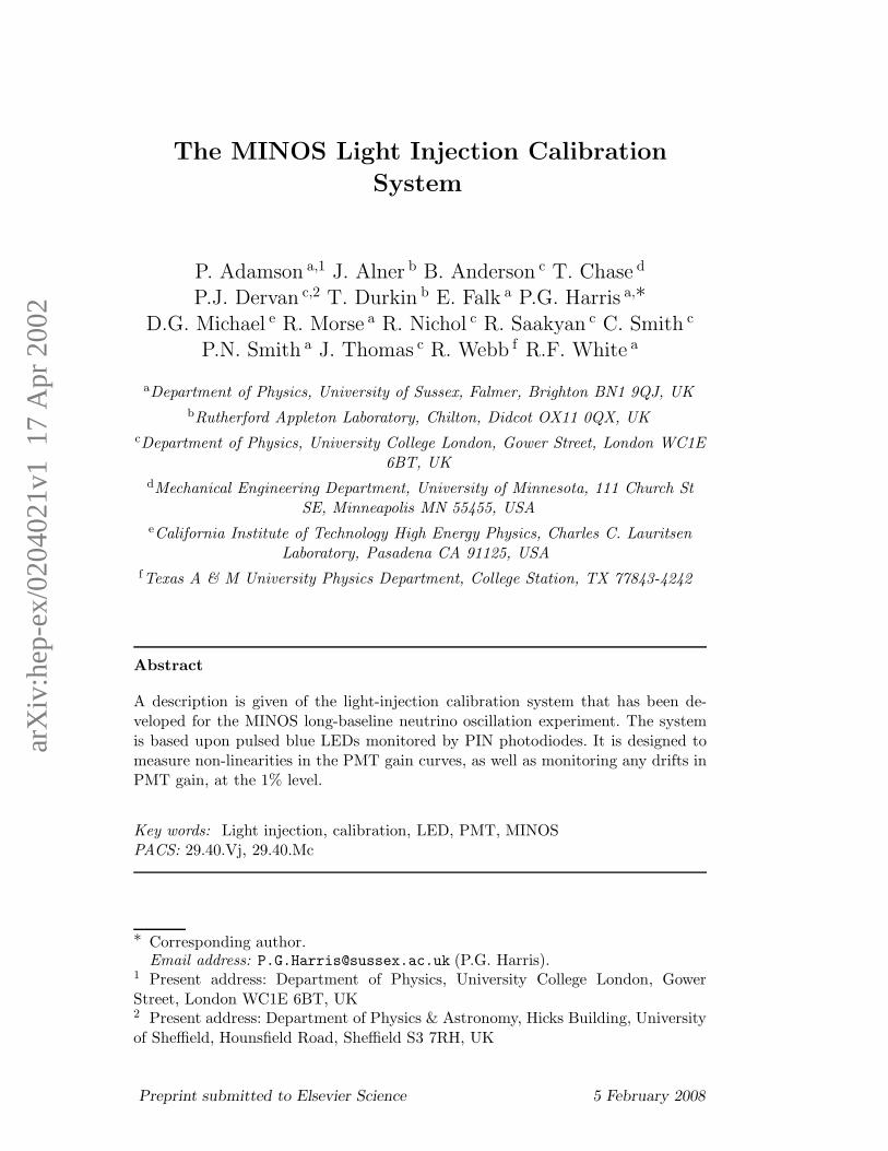
Fig. 4. Spectrum of light emitted from wavelength-shifting fibre when excited withthe light in Fig. 3.
scintillator that has itself been stimulated by a nitrogen laser [20]. In eachcase, the pulses liberated about four photoelectrons from the photocathode:this is approximately the signal size that we would expect from each end ofa MINOS far-detector scintillator strip following the passage of a minimum-ionising particle through its centre. The pulse shapes are almost identical inthe two cases, and they are dominated by the response of the WLS fibre. Ingeneral, the risetime of the LED has little effect upon the overall pulse shape.
5.6 Stability
The short-term pulse-to-pulse variation of an LED was measured by a PINphotodiode circuit with amplifier and a digital oscilloscope. The standard de-viation of the pulse height distribution, which is actually dominated by elec-tronics noise from the measurement circuit, was found to be 1.1% of the meanvalue. Therefore, when the response of the PMT to these optical pulses ismeasured, the spread in measured light levels is dominated entirely by pho-toelectron counting statistics; there is no need to account for LED variationson a pulse-by-pulse basis.
10

Fig. 5. Comparison of the average pulse shapes from WLS fibres excited by a blueLED and by laser-stimulated scintillator.
However, the LED light output does suffer occasional jumps (typically onceevery few weeks), and these can sometimes amount to changes of several per-cent. An independent measurement of light intensity is therefore needed tomonitor the output of the LED, and a PIN photodiode was chosen for thispurpose.
6 PIN photodiodes
The PIN photodiode used to monitor the relative light output from the LEDsis the Hamamatsu S5971 [6]. This was chosen primarily because it offers afast response while still having a large enough surface area to accommodatethe 1.0 mm diameter light-distribution fibres. Some characteristics are listedin Table 1.
6.1 Stability
The light injection system is required to be stable as it tracks PMT gainchanges over a period of about a month, during which time sufficient numbersof cosmic-ray muons will be detected to calibrate the detector. The stability
11

Active area size 1.2 mm diameter
Spectral response 320 nm to 1020 nm
Dark current 0.07 nA typ.
Temperature coefficient of dark current 15%/C
Photosensitivity @ 470 nm 0.24 A/W
Temperature coefficient of photosensitivity < 0.01%/C at laboratory temperatures
Table 1PIN photodiode specifications.
was tested by pulsing an LED continuously over a period of two months, andmonitoring its output several times per second with a pair of PIN photodiodes.After integration and shaping, these were read out by a digital oscilloscope(Fig. 6).
PIN Diode& amplifier
PIN Diode& amplifier
DigitalOscilloscope
Pulser PC
Fig. 6. Schematic diagram of the apparatus used to measure the PIN photodiodestability.
The results of the stability test are shown in Fig. 7. Each point in the figureis an average of a thousand consecutive readings: this is representative of theaveraging that will take place during the MINOS calibration. For clarity, onlyone data point in sixteen is plotted. Over the first ten days, the signal fromPIN 1 gradually decreased; this is thought to be caused by the fibre settlingslightly in its connector. The sudden jump in LED brightness at day 13 isunexplained, as is its instability in days 25-26; but the intensity changes wererecorded by both PIN photodiodes, and the ratio of PIN outputs remainedconstant. A weekend power cut left the system off for an extended period indays 36-38; when restarted, the LED output returned to its original value. Thefeature at 46 days occurred when the apparatus was accidently mechanicallydisturbed—a sharp deviation in one PIN’s signal is again apparent, followedby a slow return to roughly the previous level.
Although the light output of the LED changed by a few percent during thetest period (e.g. the step changes at days 13 and 37), the ratio between theindividual PIN readings remained constant to within about 0.5% over a periodof two months: this is well within the MINOS stability specification.
12

0.94
1
1.06
0 10 20 30 40 50 60Time (days)
No
rmal
ised
lig
ht
ou
tpu
tRatio of readingsPIN reading 1PIN reading 2
Fig. 7. Test of pin photodiode stability. The PINs are stable to better than 0.5%over two months.
6.2 Linearity
The PIN photodiode must provide a scale that varies linearly with appliedlight, in order to calibrate the non-linearities of the PMT. The linearity of thePIN photodiode/amplifier system was measured by comparing the signal froma pulsed LED with the signal from the same LED, but with a neutral-densityfilter blocking most of the light. The amplified and shaped output from thePIN photodiode was read out by a digital oscilloscope in peak-finding mode.Repeating this measurement for several different pulse heights spanning therange of operation of the system produced the linear response shown in Fig. 8.No evidence of non-linearity was observed.
The charge digitisation of the PIN photodiode pulse is also required to belinear. A charge-injection system calibrates the ADC readout channels to anaccuracy of 1%, thus ensuring that the PIN photodiode ADC scale is indeedproportional to the light input.
13

0
20
40
60
80
100
120
140
160
180
0 200 400 600 800 1000
High PIN reading
Att
enu
ated
PIN
rea
din
g
Fig. 8. PIN photodiode linearity. The plot shows the response in the PIN photodiodeto light from the LED pulser passing through an optical attenuator, plotted againstthe signal with no attenuation, for several different pulse heights. The uncertaintyon each point is dominated by the 8-bit readout of the digital oscilloscope, and isapproximately 0.5% of the full-scale reading on each axis.
6.3 Readout
In the far detector, two PIN photodiodes are mounted on each of the front-end readout cards. The current pulses produced by the PIN photodiodes areintegrated and amplified, producing peak voltages that are a.c. coupled tothe VA chips to achieve the required current injection. The VA chip, whoseprimary purpose is to read out PMT pulses, requires a PMT dynode signalto trigger its readout. The optical wiring ensures that the PMT that triggersthe readout of a given PIN photodiode will always be illuminated by the sameLED as the PIN photodiode in question. Each LED is in fact served by twoPIN photodiodes, mounted on separate front-end readout cards; this allowsone readout card to be replaced (to change a PMT or to replace an amplifier)whilst the LED calibration is held by the other PIN photodiode, which remainsundisturbed.
In the near detector, the phototubes are read out by QIE electronics, whichcannot be used to trigger the PIN readout. Instead, the readout of the PINphotodiodes is triggered by the presence of a signal on the dynode of a separatePMT (discussed in Section 7 below).
The optical fan-out from the LEDs is designed to deliver more light to the PIN
14

photodiode than to the PMT pixels, in order to accommodate the relativelylow sensitivity of the PIN. In this way the full dynamic range of the signalsis well matched between PIN and PMT. The signal-to-noise ratio of the PINphotodiode circuit is approximately 4000:1 at full scale.
7 Trigger PMT
At times, it will be necessary to take spectra of the PMT response at the single-photoelectron level. In a significant fraction of events no signal will then beseen in the PMT, and consequently the PIN photodiode will not be read out.In order to count these events properly, and in order to provide a distinctiveidentification to all light-injection events, each pulser box has an additionalLED that emits a consistently bright flash with each pulse, regardless of thebrightness of the primary LED pulse. Light from this additional LED is carriedto a dedicated M16 PMT – the trigger PMT – which is read out in the usualway, thus inserting a unique identifier in the data of each light-injection event.In the near detector the trigger PMT serves an additional function, in that itsdynode signal forces the readout of all PIN photodiodes.
8 Mechanical design
8.1 Pulser boxes
Each pulser box is 21 inches high, and fits in a standard 19-inch rack. It isdivided by a bulkhead wall into two compartments: one, at the front of thebox, is for electronics; the other is for fibre optics. The 20 LEDs are mountedon two circuit boards, supported on trays in the electronics compartment.A controller board, containing the microprocessor and an RS232 interface,connects the two LED driver boards.
The LEDs overhang the ends of their circuit boards and pass through holes inthe bulkhead into optical fan-outs known as cones. Each cone has a set of 71optical fibres (including spares and dedicated, centrally-located fibres to carrylight to PIN photodiodes). These fibres take the optical signals from the conesto four columns of 16 connectors on the back panel (Fig. 9) of the box; eachback-panel connector holds 20 fibres – one from each cone. There are threeadditional 20-wide connectors on the back panel — two provide light to thePIN photodiodes (and so are fed by the dedicated PIN photodiode fibres), andthe third is a spare. There is also a single-fibre connector carrying light to thetrigger PMT.
15

Fig. 9. The rear compartment of a pulser box, showing the back-panel connectors.The side panels have been removed, and the collars at the end of each of the tworows are visible. A fibre from each collar runs to each 20-wide connector. Photographcourtesy OMC ltd.
Bundles of 20 fibres mounted externally to the box transport the light fromeach of the back-panel connectors to the 20 light-injection points on each sideof each far-detector plane; this is illustrated in Figure 10. The optical routingin the near detector is identical, except that there are fewer light-injectionpoints on each plane (eleven for fully instrumented planes, seven for partiallyinstrumented planes, and on one side of the detector only). The calibrationdetector has just three light-injection points on each side of each of its 60planes, and is thus served by six LEDs in a single pulser box.
8.2 Cones and ponytails
The basic design for the optical fan-out is a conical hole bored longitudinallythrough an aluminium cylinder, with the LED seated at the apex and the71-fibre bundle attached at the base, as shown in Fig. 11. The walls of thecone are lined with aluminised polyester (with a reflectivity greater than 99%)to maximise the intensity of light delivered to the fibres and to assist with theuniformity of illumination of the fibre bundle. The fibre bundle, or “ponytail”,
16

Fig. 10. Schematic showing typical optical routing for the far detector light injectionsystem. On certain planes, multiplexing constraints require that the ordering offibres within a bundle is changed: but the basic pattern wherein each of the 6420-way connectors contains a fibre from each LED, and a fibre bundle from eachsuch connector feeds in turn one half of a single detector plane, always holds.
is glued into a plastic collar which is attached to the cone. During assembly,the ends of the fibres are positioned precisely within the collar by means of aplastic disc with holes drilled in it, known as a “tea-strainer”. The surface ofthis is fly-cut with a diamond-tipped tool.
Three fibres (including one spare) are designated to serve the PIN photodi-
17

Stripped 68−fibre bundle Collar
Potting
Unstripped 71−fibre bundle
O−ring
Internal panel of pulser box
Stripped set of 3 fibres for PIN
Surface of conical holeto be lined withaluminised polyester film
LED leadalignment disc
68−hole fibre plate
Tube for PIN fibres
LED
Cone
Fig. 11. Cone and collar assembly for pulser box.
odes. These are placed in the centre of the fibre bundle. To provide morelight, these fibres are extended towards the LED, and are encased in a rigidplastic tube for support (see Fig. 11). This also assists in reducing the non-uniformity of illumination of the light-injection fibres, as the PIN photodiodefibres occupy the area of brightest illumination. Fig. 12 shows the uniformityof illumination of a typical fibre tea-strainer. In this example, the RMS de-viation is approximately 15% of the mean value, and the ratio of maximumto minimum intensities is 2.28. On later production models the uniformityimproved somewhat, with the ratio of maximum to minimum intensities oftenlying below 2.0.
Fig. 12. Uniformity of illumination of a fibre tea-strainer with a wide-angle LED.The area of each circle is proportional to the intensity of illumination. The bundleincluded three spare fibres whose outputs were not measured.
18

The PIN photodiode fibres are significantly longer than all other fibres in theponytail (6 m vs. 0.8 m). This minimises the differences in relative arrivaltimes of the optical pulses at the PIN photodiodes and at the PMT photo-cathodes, by compensating for the different optical path lengths: this ensuresin turn that the amplified and shaped pulse from the PIN photodiode readoutcircuit is sampled and digitised at its peak.
A disassembled cone and collar are shown in Fig. 13.
Fig. 13. A collar and cone. The tea-strainer and the central tube holding the PINphotodiode fibres are seen at the front of the collar, and the fibre bundle (ponytail)is emerging from its rear.
8.3 Optical fibre
The optical fibre used has a 1 mm diameter core of polymethyl methacrylate,with a fluorinated polymer cladding, and was manufactured by MitsubishiCorp. [21]. The attenuation at 473 nm (the wavelength of the blue LEDs) isapproximately 0.08 dB/m. The fibre is jacketed with 2.2 mm diameter opaqueblack PVC that has a UL-VW1 [22] flame-resistance rating, a fire-safety re-quirement.
8.4 Optical connectors
The multi-fibre connectors, both at the rear of the pulser box and on themating ends of the external fibre bundles, are made of plastic. Once the fibreshave been glued into place, the connectors are fly-cut with a diamond-tipped
19

tool: this provides extremely good optical transmission, of up to 90% for eachconnector pair, without damaging the fibres and with a considerable saving inmanpower over a hand-polishing process. The design for these connectors wasadapted from that for the MINOS optical readout connectors.
Individual fibre ends in the light-injection system are all terminated with anH19 metal connector from OMC [23] (for those carrying light to the PINphotodiodes) or a custom-made, slightly larger variant thereof known as theCLRC01 (for those plugged into the light-injection points on the detector).After gluing and light crimping into the connector, these fibre ends are hand-polished to optimise transmission.
9 Light injection modules
Fig. 14. Manifold parts. The light-injection module, here shown detached, forms thecover to the end of the manifold. The exteriors of the two “ashtray” compartmentsare marked.
20
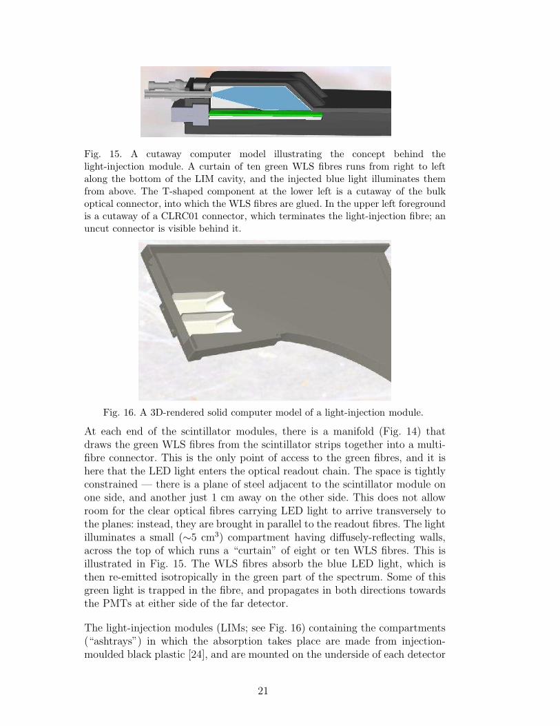
Fig. 15. A cutaway computer model illustrating the concept behind thelight-injection module. A curtain of ten green WLS fibres runs from right to leftalong the bottom of the LIM cavity, and the injected blue light illuminates themfrom above. The T-shaped component at the lower left is a cutaway of the bulkoptical connector, into which the WLS fibres are glued. In the upper left foregroundis a cutaway of a CLRC01 connector, which terminates the light-injection fibre; anuncut connector is visible behind it.
Fig. 16. A 3D-rendered solid computer model of a light-injection module.
At each end of the scintillator modules, there is a manifold (Fig. 14) thatdraws the green WLS fibres from the scintillator strips together into a multi-fibre connector. This is the only point of access to the green fibres, and it ishere that the LED light enters the optical readout chain. The space is tightlyconstrained — there is a plane of steel adjacent to the scintillator module onone side, and another just 1 cm away on the other side. This does not allowroom for the clear optical fibres carrying LED light to arrive transversely tothe planes: instead, they are brought in parallel to the readout fibres. The lightilluminates a small (∼5 cm3) compartment having diffusely-reflecting walls,across the top of which runs a “curtain” of eight or ten WLS fibres. This isillustrated in Fig. 15. The WLS fibres absorb the blue LED light, which isthen re-emitted isotropically in the green part of the spectrum. Some of thisgreen light is trapped in the fibre, and propagates in both directions towardsthe PMTs at either side of the far detector.
The light-injection modules (LIMs; see Fig. 16) containing the compartments(“ashtrays”) in which the absorption takes place are made from injection-moulded black plastic [24], and are mounted on the underside of each detector
21

module, thus forming part of the manifold cover (see Fig. 14). The 16- and20-wide scintillator modules have two ashtrays in each LIM, and the widermodules have three. A complete MINOS far-detector plane contains 192 scin-tillator strips, whose green fibres are divided amongst a total of 20 ashtrays.Each ashtray is supplied with the blue light from a single plastic fibre, de-rived ultimately from one of the 20 LEDs in a pulser box. Each of the LEDsilluminates the same ashtray in up to 64 planes.
0
20
40
60
80
100
120
140
1 2 3 4 5 6 7 8 9 10
Fibre number
Illu
min
atio
n (
arb
. un
its)
Fig. 17. Uniformity of illumination of the ten fibres in a light-injection module“ashtray”.
As discussed earlier, the total amount of light illuminating each of the wavelength-shifting fibres should be as uniform as possible. The central position of thelight-injection fibre in each ashtray results in a stronger illumination of thefibres at the centre than at the edges of the ashtray. This tendency is coun-tered to some extent by incorporating a curved reflecting back, as shown inFig. 16, which both shades a portion of the central fibres and reflects morelight towards the edges than would a flat back. The uniformity of responseacross the ashtray is shown in Fig. 17. The walls of each ashtray are coatedwith a highly reflective TiO2-based paint (Bicron BC625).
10 Optical routing constraints
The far detector is eight-fold optically multiplexed. It is essential that only onefibre is illuminated at any one time on any given pixel. As eight or ten adjacentfibres are illuminated simultaneously in an ashtray, this places a constraint on
22

the multiplexing pattern used — any scheme where adjacent strips are mappedto the same pixel is not permissible.
Fig. 18. Chessboard illumination pattern for M16s in the far detector. Pixels arenumbered from right to left and top to bottom when viewing the face of the PMT.The shaded pixels are illuminated by a single ashtray, and are therefore illuminatedsimultaneously by light from the same LED. Note that no two edge-adjacent pixelsare illuminated at the same time.
It is also desirable to avoid simultaneous pulsing of adjacent PMT pixels, inorder to mitigate the effects of crosstalk [11]. This is the reason for only il-luminating up to 10 WLS fibres (one ashtray) at any one time in any givenplane. Arranging the fibres from sequential scintillator strips on alternate M16pixels ensures that the pixels are illuminated in a chessboard pattern, as inFig. 18, with diagonal rather than edge-adjacent pixels being illuminated si-multaneously. The mapping is staggered on one side of the plane so that a hitcan be located in the plane by using both ends of the readout.
These considerations lead to a simple algorithm for the optical wiring of thepulser boxes. Each connector at the back of the pulser box contains one fibrefrom each of the 20 LEDs, and the 20 fibres from each such connector feedthe 20 ashtrays of one end of a single plane. Thus, any given LED illuminatesup to ten green fibres on each of 64 planes.
11 Electronics
The LED pulser offers the ability to change both the height and the widthof the pulse electronically, by varying the current pulse that is applied tothe LED. Each pulser box contains up to 20 LEDs, although in the neardetector only 11 LEDs are used. As discussed in Section 7, the controller cardincorporates an additional “trigger” LED that pulses at a fixed intensity andwhich is used to flag light-injection events in the data stream.
23

11.1 Pulser control
The pulser box is controlled by a PIC16F877 microprocessor [25]. It commu-nicates with a control PC via ASCII commands over a serial RS232 link. Toavoid a proliferation of different types of data-carrying cable running aroundthe detector, the signals are carried over the detector Ethernet, and convertedfor the pulser box by an Ethernet-RS232 converter. In the standard mode ofoperation, the PC instructs the system to pulse a given LED a certain numberof times (typically 1000) at a given height, width, and frequency (from 0.5 Hzto 1 kHz). The microprocessor then controls the actual pulsing. The pulserbox is also supplied with an external trigger input, which forces a pulse of itscurrent height/width setting in response to a TTL signal. This can be usedin the near detector to investigate the effects of the timing of a pulse withrespect to the 19 ns time buckets in the QIE electronics.
Fig. 19. LED pulser drive circuitry.
Fig. 19 shows the LED driver stage from the pulser box circuit. The appliedvoltage, which determines the pulse height, is controlled by a 10-bit DAC.When the signal at A goes high, the driver stage is turned on — voltage isapplied to the 22 Ω resistor, and the current is shunted to ground via theleft-hand FET. This occurs typically a microsecond before the actual pulse,
24

to give the current time to stabilise. (This “bypass” current is turned offbetween each pulse in order to avoid excessive heating.) When the signal at Bgoes low, current flows through the LED, which emits light. A short time later,signal C goes high, and the current is shunted to ground via the right-handFET; the LED is then turned off. The pulse width is determined by the delaybetween B turning off and C turning on; this is controlled by a programmabledelay line, giving a current pulse width of 15 to 36 ns in 3 ns steps. The lightpulses delivered to the phototube produce signals ranging from a fraction ofa photoelectron up to about 500 photoelectrons.
12 Performance
During the summer of 2001, the MINOS calibration detector was placed in acharged-particle test beam at CERN. One of its functions was to confirm thatthe light-injection system could compensate for changing PMT gains at the1% level. The calibration detector was fully equipped with MINOS readoutelectronics.
The gain curves of the PMTs were produced by injecting light at ten differentlevels, and plotting the response of the PMTs as a function of the PIN pho-todiode output. Figure 20 shows two such plots, labelled “Old Gain Curve”and “New Gain Curve”, measuring the same channel at different times. Eachpoint represents the mean µ of 2000 optical pulses. The gain in general wasobserved to drift only slowly (less than 2% over two months); but at one pointthe voltage supplied to the PMTs was increased, resulting in the dramaticdifference between the two gain curves shown here.
Drift in gain is monitored by looking at specific points on the gain curve ona regular (typically hourly) basis, as discussed in Section 4.1 above. Thesepoints are used to calculate a multiplicative factor for each channel that isapplied to the entire gain curve so as to mimic the time-evolution of the gain.The underlying assumption is that the actual shape of the gain curve does notchange on a short timescale. Figure 20 includes the recalculated gain-curvepoints.
The performance of the light-injection system can therefore be tested by se-lecting different points on the gain curves, and comparing the mean ADC fora given light input with that predicted from the drift-point calculation. Theresults of this procedure are shown in Figure 21. The upper histogram showsthe relative difference between the means of measured points on separate gaincurves, i.e. (ADC(0)-ADC(t))/ADC(0), and the lower histogram shows the rel-ative difference between the measured and corrected points, i.e. (ADC(0)corr-ADC(t))/ADC(0)corr. This technique is independent of any changes in light
25

Fig. 20. Photomultiplier gain curves. For several different intensities of injected light,the response of the PMT is shown as a function of the PIN photodiode output. “OldGain Curve” and “New Gain Curve” were taken at different values of the supplyvoltage; the light-injection system was used to provide a mapping from the old tothe new curve, and thus to measure the large change in gain.
output from the LEDs; any change in gain of the PIN photodiodes would ap-pear as an offset from zero of the lower histogram. The width of the lower his-togram is limited by photoelectron counting statistics at each data point: theultimate precision achievable by the system is not yet completely determined,but the figure demonstrates that the calibration procedure has corrected thegain changes to within the 1% specification required by MINOS.
13 Conclusion
A light-injection system has been developed to assist in the calibration of theMINOS detectors. Based upon blue LEDs, with PIN photodiodes to monitorrelative intensities, the system is able to measure non-linearities in PMT re-sponse as well as measuring changes in gain at the 1% level on an hourly basisover timescales of a month or more.
Acknowledgements
This work has been funded by the UK Particle Physics and Astronomy Re-search Council and the US Department of Energy. The authors would like tothank the other members of the MINOS collaboration for their support, and inparticular Jim Musser and Karol Lang, both of whom have provided valuable
26
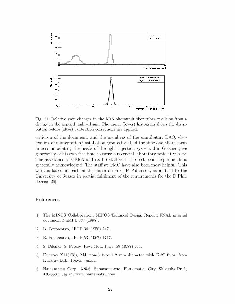
Fig. 21. Relative gain changes in the M16 photomultiplier tubes resulting from achange in the applied high voltage. The upper (lower) histogram shows the distri-bution before (after) calibration corrections are applied.
criticism of the document, and the members of the scintillator, DAQ, elec-tronics, and integration/installation groups for all of the time and effort spentin accommodating the needs of the light injection system. Jim Grozier gavegenerously of his own free time to carry out crucial laboratory tests at Sussex.The assistance of CERN and its PS staff with the test-beam experiments isgratefully acknowledged. The staff at OMC have also been most helpful. Thiswork is based in part on the dissertation of P. Adamson, submitted to theUniversity of Sussex in partial fulfilment of the requirements for the D.Phil.degree [26].
References
[1] The MINOS Collaboration, MINOS Technical Design Report; FNAL internaldocument NuMI-L-337 (1998).
[2] B. Pontecorvo, JETP 34 (1958) 247.
[3] B. Pontecorvo, JETP 53 (1967) 1717.
[4] S. Bilenky, S. Petcov, Rev. Mod. Phys. 59 (1987) 671.
[5] Kuraray Y11(175), MJ, non-S type 1.2 mm diameter with K-27 fluor, fromKuraray Ltd., Tokyo, Japan.
[6] Hamamatsu Corp., 325-6, Sunayama-cho, Hamamatsu City, Shizuoka Pref.,430-8587, Japan; www.hamamatsu.com.
27

[7] G. Feldman, report of the MINOS Calibration Working Group; unpublished.
[8] P. Litchfield, Presentation to minos calibration working group.
[9] R. Lee, S. Seun, FNAL internal document NuMI-L-694 .
[10] Kuraray 1.2 mm diameter clear fibre, from Kuraray Ltd., Tokyo, Japan.
[11] S. E. K. Lang, J. Day, et al., Nucl. Instr. Meth. A 461 (2001) 571–573.
[12] O. Toker, S. Masciocchi, E. Nygard, A. Rudge, P. Weilhammer, Nucl. Instr.Meth. A 340 (1994) 572–579.
[13] IDE AS, Veritasveien 9, Box 315, N-1323 Hvik, Norway; www.ideas.no.
[14] T. Zimmerman, M. Sarraj, IEEE Trans. on Nuclear Science 43 (1996) 1683–1688.
[15] Hewlett-Packard 3000 Hanover Street Palo Alto, CA 94304-1185, U.S.A.;www.hp.com.
[16] Nichia Corporation, 491 Oka, Kaminaka-Cho, Anan, Tokushima 774-8601,Japan; www.nichia.co.jp.
[17] J. Thomas, et al., Nucl. Instr. Meth. A 423 (1999) 320–327.
[18] P. Border, et al., Nucl. Instr. Meth. A 463 (2001) 194–204.
[19] B. Choudhary, L. Mualem, FNAL internal document NuMI-L-589 .
[20] R. Schwienhorst, private communication; data provisionally available athttp://www.hep.umn.edu/minos/fiber/timing.html.
[21] Mitsubishi Rayon Corp., 520 Madison Avenue, New York, NY 10022, U.S.A.;www.mitsubishi.com.
[22] Underwriters Laboratories; www.ul.com. The VW1 test is described in standardUL 1581, section 1080.
[23] Optoelectronic Manufacturing Corporation, Redruth, Cornwall, U.K.;www.optomanfcorp.com.
[24] Polyphenylene Oxide - Styrene (NorylTM grade N190X); www.geplastics.com.
[25] Microchip Technology Inc., Chandler, Arizona, U.S.A.; www.microchip.com.
[26] P. Adamson, An LED Calibration System for the MINOS Long-BaselineNeutrino Oscillation Experiment, D.Phil. Thesis, University of Sussex (2001).
28