THE LEFT HAND OF ELECTROMAGNETISM: METAMATERIALS · the left hand of electromagnetism:...
187
THE LEFT HAND OF ELECTROMAGNETISM: METAMATERIALS A THESIS SUBMITTED TO THE DEPARTMENT OF PHYSICS AND THE INSTITUTE OF ENGINEERING AND SCIENCES OF BILKENT UNIVERSITY IN PARTIAL FULLFILMENT OF THE REQUIREMENTS FOR THE DEGREE OF DOCTOR OF PHILOSOPHY By Kamil Boratay ALICI October, 2010
Transcript of THE LEFT HAND OF ELECTROMAGNETISM: METAMATERIALS · the left hand of electromagnetism:...

THE LEFT HAND OF
ELECTROMAGNETISM: METAMATERIALS
A THESIS
SUBMITTED TO THE DEPARTMENT OF PHYSICS
AND THE INSTITUTE OF ENGINEERING AND SCIENCES
OF BILKENT UNIVERSITY
IN PARTIAL FULLFILMENT OF THE REQUIREMENTS
FOR THE DEGREE OF
DOCTOR OF PHILOSOPHY
By
Kamil Boratay ALICI
October, 2010

ii
I certify that I have read this thesis and that in my opinion it is fully adequate, in
scope and in quality, as a thesis for the degree of Doctor of Philosophy.
Prof. Dr. Ekmel Özbay (Supervisor)
I certify that I have read this thesis and that in my opinion it is fully adequate, in
scope and in quality, as a thesis for the degree of Doctor of Philosophy.
Prof. Dr. Atilla Erçelebi
I certify that I have read this thesis and that in my opinion it is fully adequate, in
scope and in quality, as a thesis for the degree of Doctor of Philosophy.
Assoc. Prof. Dr. Vakur B. Ertürk
I certify that I have read this thesis and that in my opinion it is fully adequate, in
scope and in quality, as a thesis for the degree of Doctor of Philosophy.
Assoc. Prof. Dr. M. Özgür Oktel

iii
I certify that I have read this thesis and that in my opinion it is fully adequate, in
scope and in quality, as a thesis for the degree of Doctor of Philosophy.
Assoc. Prof. Dr. Hamza Kurt
Approved for the Institute of Engineering and Sciences:
Prof. Dr. Levent Onural
Director of Institute of Engineering and Sciences

iv
ABSTRACT
THE LEFT HAND OF ELECTROMAGNETISM:
METAMATERIALS
Kamil Boratay ALICI
PhD in Physics
Supervisor: Prof. Dr. Ekmel Özbay
October, 2010
Metamaterials are artificial periodic structures whose electromagnetic
response is solely dependent on the constituting unit cells. In the present thesis,
we studied unit cell characteristics of metamaterials that has negative
permeability and permittivity. We investigated negative permeability medium
elements, especially in terms of their electrical size and resonance strength.
Experimental and numerical study of µ-negative (MNG) materials: multi split
ring resonators (MSRRs), spiral resonators (SRs) and multi-spiral resonators are
presented. The resonance frequency of the structures is determined by the
transmission measurements and minimum electrical size of λ0/17 for the MSRRs
and of λ0/82 for the SRs observed. We explain a method for tuning the
resonance frequency of the multi-split structures. We investigated scalability of
MNG materials and designed a low loss double negative composite
metamaterial that operates at the millimeter wave regime. A negative pass-band
with a peak transmission value of -2.7 dB was obtained experimentally at 100
GHz. We performed transmission based qualitative effective medium theory
analysis numerically and experimentally, in order to prove the double negative
nature of the metamaterial. These results were supported by the standard
retrieval analysis method. We confirmed that the effective index of the
metamaterial was indeed negative by performing far field angular scanning
measurements for a metamaterial prism. Moreover, we illuminated the split-ring
resonator based metamaterial flat lens with oblique incidence and observed from
the scanning experiments, the shifting of the beam to the negative side. The first

v
device was a horn antenna and metamaterial lens composite whose behavior was
similar to Yagi-Uda antenna.
We numerically and experimentally investigated planar fishnet metamaterials
operating at around 20 GHz and 100 GHz and demonstrated that their effective
index is negative. The study is extended to include the response of the
metamaterial layer when the metamaterial plane normal and the propagation
vector are not parallel. We also experimentally studied the transmission
response of a one dimensional rectangle prism shaped metamaterial slab for
oblique incidence angles and confirmed the insensitivity of split-ring resonator
based metamaterials to the angle of incidence. After the demonstration of
complete transmission enhancement by using deep subwavelength resonators
into periodically arranged subwavelength apertures, we designed and
implemented a metamaterial with controllable bandwidth.
The metamaterial based devices can be listed under the categories of antennas
absorbers and transmission enhancement. We studied electrically small resonant
antennas composed of split ring resonators (SRR) and monopoles. The electrical
size, gain and efficiency of the antenna were λ0/10, 2.38 and 43.6%,
respectively. When we increased the number of SRRs in one dimension, we
observed beam steerability property. These achievements provide a way to
create rather small steerable resonant antennas. We also demonstrated an
electrically small antenna that operates at two modes for two perpendicular
polarizations. The antenna was single fed and composed of perpendicularly
placed metamaterial elements and a monopole. One of the metamaterial
elements was a multi split ring resonator and the other one was a split ring
resonator. When the antenna operates for the MSRR mode at 4.72 GHz for one
polarization, it simultaneously operates for the SRR mode at 5.76 GHz, but for
the perpendicular polarization. The efficiencies of the modes were 15% and 40%
with electrical sizes of λ/11.2 and λ/9.5. Finally, we experimentally verified a
miniaturization method of circular patch antennas. By loading the space between

vi
the patch and ground plane with metamaterial media composed of multi-split
ring resonators and spiral resonators, we manufactured two electrically small
patch antennas of electrical sizes λ/3.69 and λ/8.26. The antenna efficiency was
40% for the first mode of the multi-split ring resonator antenna with broad far
field radiation patterns similar to regular patch antennas.
We designed, implemented, and experimentally characterized electrically thin
microwave absorbers by using the metamaterial concept. The absorbers consist
of i) a metal back plate and an artificial magnetic material layer; ii) metamaterial
back plate and a resistive sheet layer. We investigated absorber performance in
terms of absorbance, fractional bandwidth and electrical thickness, all of which
depend on the dimensions of the metamaterial unit cell and the distance between
the back plate and metamaterial layer. As a proof of concept, we demonstrated a
λ/4.7 thick absorber of type i), with a 99.8% absorption peak along with a 8%
fractional bandwidth. We have also demonstrated experimentally a λ/4.7 and a
λ/4.2 thick absorbers of type ii), based on SRR and MSRR magnetic
metamaterial back plates, respectively. The absorption peak of the SRR layout is
97.4%, while for the MSRR one the absorption peak is 98.4%. We conveyed
these concepts to optical frequencies and demonstrated a metamaterial inspired
absorber for solar cell applications.
We finalized the study by a detailed study of split ring resonators at the
infrared and visible band. We studied i) frequency tuning, ii) effect of resonator
density, iii) shifting magnetic resonance frequency by changing the resonator
shape, iv) effect of metal loss and plasma frequency and designed a
configuration for transmission enhancement at the optical regime. By using
subwavelength optical split ring resonator antennas and couplers we achieved a
400-fold enhanced transmission from a subwavelength aperture area of the
electrical size λ2/25. The power was transmitted to the far field with 3.9 dBi
directivity at 300 THz.

vii
Keywords: Metamaterial, Antenna, Absorber, Solar Cell, Miniaturization,
Multiple Split Ring Resonator, Spiral Resonator, Multiple Spiral Resonator,
Negative Permittivity, Negative Permeability, Negative Refraction, Planar
Metamaterial, Oblique Response, Split Ring Resonator Antenna, Dual Band
Antenna, Electrically Thin Absorber, Photonic Metamaterial.

viii
ÖZET
ELEKTROMANYETĠĞĠN SOL ELĠ:
METAMALMEZELER
Kamil Boratay ALICI
Fizik Bölümü, Doktora
Tez Yöneticisi: Prof. Dr. Ekmel Özbay
Ekim 2010
Metamalzemeler elektromanyetik özellikleri onları oluşturan birim hücrelere
bağlı olan periyodik yapay yapılardır. Bu tezde, ilk olarak metamalzemelerin
negatif permeabilite ve negatif permitivite birim hücre özelliklerini inceledik.
Negatif permeabilite sağlayan birim hücreleri özellikle elektriksel boyut ve
rezonans gücü açılarından araştırdık. Çoklu yarıklı halka rezonatörlerinin
(MSRR) ve sarmal rezonatörlerin (SR) deneysel ve sayısal çalışmasını sunduk.
Ġletim ölçümlerinden bu yapıların rezonans frekansını belirledik ve SR‟lar için
λ0/82, MSRR‟lar için λ0/17 minimum elektriksel boyutları elde ettik. Bu
ölçümlerde λ0 serbest uzay dalga boyunu ifade etmektedir. Çok yarıklı yapılar
için rezonans frekansını ayarlama yöntemi keşfettik. Çifte negatif kompozit
metamalzemelerin ölçeklenebilirliğini kullanarak bu yapıları milimetre
dalgaboyunda düşük kayıpla çalışır halde tasarladık ve ölçtük. Geçirgen banttaki
zirve değeri -2,7 dB olan ve 100 GHz‟de çalışan yapıları deneysel olarak
gösterdik. Çifte negatif özelliği kanıtlamak için sayısal ve deneysel olarak iletim
tabanlı etkisel ortam kuramını uyguladık. Bu sonuçları standart alım analizi ile
destekledik. Prizma şeklindeki bir metamalzeme yapıp etkin kırınım indeksinin
açısal tarama ölçümleri ile negatif olduğu doğruladık. Dahası, yarıklı halka
rezonatör tabanlı düz bir metamalzemeyi eğik açıyla aydınlatıp iletilen gücü
tarama deneyleri ölçerek ışığın negatif tarafa kırıldığını gözlemledik. Son olarak
bu düz metamalzemeyi boynuz antenin önüne koyduğumuzda davranışının
Yagi-Uda antene benzer olduğunu gördük.

ix
Sayısal ve deneysel olarak düzlemsel balık ağı metamalzemelerini yaklaşık 20
GHz ve 100 GHz‟de çalıştığını gösterdik ve onların etkin kırınım indislerinin
negatif olduğunu kanıtladık. Çalışmamız metamalzeme tabakaları ile yayılma
vektörünün paralel olmadığı durumu da içermektedir. Eğik açılarla gelen
dalgalar için yarıklı halka rezonatörü temelli metamalzemelerin yanıtı
değişmemektedir. Ayrıca dalga boyu altı boyutlu periyodik deliklerden geçen
güç dalga boyu altı rezonatörler kullanılarak arttırıldı ve tam iletim
sağlanabileceği gösterildi.
Metamalzeme tabanlı cihazlar, antenler, soğurucular ve arttırılmış iletim yapıları
olarak sıralanabilir. Elektriksel olarak küçük, yarıklı halka rezonatörü ve tel
antenden oluşan antenler tasarladık. Bu antenlerin elektriksel boyutu, kazancı ve
verimliliği sırasıyla λ0/10, 2.38 ve % 43.6 idi. Bu antendeki yan yana dizilmiş
SRR sayısı arttığında yaydığı radyasyonun yönü de değişmektedir. Bu küçük
antenler fazlı dizi antenlerinin birim elemanı olarak kullanılabilir. Ayrıca, iki
çoklu halka rezonatörü birbirine dik konumda kullanarak iki değişik frekansta ve
polarizasyonda çalışan bir elektriksel olarak küçük anten gösterdik. Bu anten bir
polarizasyon için 4.72 GHz‟de diğer polarizasyon için 5.76 GHz‟de
çalışmaktadır. Verimliliği ise sırasıyla % 15 ve % 40, elektriksel boyutu ise
sırasıyla λ/11.2 ve λ/9.5‟tur. Son olarak, yuvarlak yama antenlerini
minyatürleştirmek için bir yöntem gösterdik. Bu antendeki yama ve toprak
düzlemi arasındaki boşluğa rezonatörleri dizerek λ/3.69 ve λ/8.26 elektriksel
boyuta sahip yama antenler gösterdik. Bu antenin radyasyon yayılımı, normal
yama anteninkine benzerken boyutu daha küçük ve verimi % 40‟tır.
Metamalzemelerin küçük elektriksel boyutlarından faydalanarak ince
mikrodalga radyasyon soğurucular tasarladık. Bu soğurucular i) metal bir arka
plaka ve yapay bir manyetik metamalzeme tabakasından, ii) metamalzeme arka
plaka ve dirençli sac tabakadan oluşur. Soğurucu performansını çalıştığı kesirli
bant genişliği ve elektriksel kalınlığı açılarından inceledik. Tip i) soğurucu için

x
% 8 kesirli bant genişliği ve % 99.8 tepe soğurma değeri olan λ/4.7 kalınlıkta bir
soğurucu gösterdik. Kullanılan rezonatörün elektriksel boyutuna bağlı olarak
soğurucu kalınlığı değişmektedir. Bu kavramlar optik frekanslar için de
geçerlidir ve güneş pili gibi birçok uygulama için ümit vericidir.
Periyodik yarıklı halka rezonatörleri kızılötesi ve görünür bantlarda da
çalışılabilir. Biz bu çalışmada i) rezonatör şeklini değiştirerek manyetik
rezonans frekansının değiştiğini, ii) periyodik dizilimde rezonatör yoğunluğunun
etkisini iii) metal kaynaklı kayıpları ve metal plazma frekansının etkisini
gösterdik. Optik rejimde arttırılmış iletim için dalga boyu altı yarıklı halka
rezonatör antenleri ve kuplörleri kullanarak elektriksel boyutu λ2/25 olan bir
delikten 400 kat arttırılmış iletim elde ettik. Bu güç uzak alana 300 THz
frekansta 3.9 dBi yönlülük ile aktarılmaktadır.
Anahtar Kelimeler: Metamalzeme, Anten, Soğurucu, Solar Hücre, Minyatür
çoklu yarıklı halka rezonatörü, Sarmal rezonatör, Çoklu Sarmal rezonatör,
Negatif kırınım indisi, Negatif Kırılma, Düzlemsel Metamalzeme, Eğik açıyla
gelen ışık durumu, yarıklı halka rezonatör Anteni, Dual Bant Anten, Elektriksel
olarak ince soğurucu , fotonik Metamalzeme.

xi
Acknowledgements
I would like to thank Prof. Dr. Ekmel Özbay for his great patience and excellent
guidance throughout my PhD study.
I would like to thank to The Scientific and Technological Research Council of
Turkey (TUBITAK) for awarding me with the graduate scholarship.
I would like to thank to the members of my thesis committee, Assoc. Prof. Dr.
Vakur B. Ertürk, Assoc. Prof. Dr. Mehmet Özgür Oktel, Assoc. Prof. Dr. Hamza
Kurt, and Prof. Dr. Atilla Erçelebi for reading the manuscript and commenting
on the thesis.
I would like to thank to Advanced Research Laboratory staff, Physics
Department Laboratory staff and Nanotechnology Research Center group
members who had a positive effect on my research.
I would like to thank my friends Serkan Bütün for fruitful scientific discussions
and Onur Atuğ for listening my complaints throughout the graduate study.
I would like to thank to my parents, my sister and especially my fiancée for her
great support without which I could not be successful.

1
Table of Contents
ACKNOWLEDGEMENTS ............................................................................. Xİ
INTRODUCTION ............................................................................................ 14
1.1 OUTLINE OF THE THESIS .......................................................................................................... 15
METAMATERIAL ELEMENTS FOR ARTIFICIAL MAGNETISM ...... 21
2.1. INTRODUCTION ...................................................................................................................... 21
2.1.1. EXPERIMENT SETUP ........................................................................................................... 23
2.1.2 NUMERICAL METHOD ......................................................................................................... 24
2.2. MULTIPLE SPLIT RING RESONATORS ..................................................................................... 24
2.3. SPIRAL RESONATORS ............................................................................................................. 26
2.4. MULTI-SPIRAL RESONATORS ................................................................................................. 28
2.5. EFFECT OF RESONATOR PARAMETERS ON THE ELELCTRICAL SIZE ...................................... 30
2.6. SUBSTRATE EFFECTS AND SIZE SCALING .............................................................................. 33
2.7. TUNABILITY OF MULTI SPLIT RESONATORS .......................................................................... 35
2.8. TEMPERATURE DEPENDENT RESONATOR RESPONSE ............................................................. 36
MILLIMETER-WAVE SCALE METAMATERIALS WITH NEGATIVE-
INDEX OF REFRACTION ............................................................................. 45
3.1. INTRODUCTION ...................................................................................................................... 45
3.2. DESIGN AND EXPERIMENT ..................................................................................................... 47
3.3. TRANSMISSION BASED QUALITATIVE EFFECTIVE MEDIUM THEORY ANALYSIS .................... 49
3.4. RETRIEVAL ANALYSIS ........................................................................................................... 51
3.5. LOSS AND BANDWIDTH ANALYSIS ........................................................................................ 53
3.6. DIRECT OBSERVATION OF NEGATIVE REFRACTION ............................................................... 54
3.7. STUDY OF A METAMATERIAL PRISM ...................................................................................... 59
3.8. FAR FIELD RADIATION BEHAVIOR OF HORN ANTENNA AND METAMATERIAL COMPOSITE ... 63
PLANAR METAMATERIALS ...................................................................... 66
4.1. INTRODUCTION ...................................................................................................................... 66
4.2. CURRENT DISTRIBUTION, TRANSMISSION AND RETRIEVAL ANALYSES FOR 20 GHZ ............. 68
4.3. 100 GHZ FISHNET METAMATERIAL DESIGN .......................................................................... 74
4.4. CURRENT DISTRIBUTION, TRANSMISSION AND RETRIEVAL ANALYSES FOR 100 GHZ ........... 75

2
OBLIQUE RESPONSE OF FLAT METAMATERIAL SLABS ................ 81
5.1. INTRODUCTION ...................................................................................................................... 81
5.2. TRANSMISSION BASED QUALITATIVE EFFECTIVE MEDIUM THEORY OF A SRR BASED
METAMATERIAL ........................................................................................................................... 82
5.3. INCIDENT ANGLE DEPENDENT TRANSMISSION RESPONSE OF SRR BASED METAMATERIALS 85
5.4. OBLIQUE RESPONSE OF FISHNET METAMATERIALS ............................................................... 87
METAMATERIAL INSPIRED ELECTRICALLY SMALL ANTENNAS 89
6.1. INTRODUCTION ...................................................................................................................... 89
6.1.1. ELECTRICALLY SMALL ANTENNA CHARACTERIZATION BASICS ........................................ 90
6.1.1.1. PARAMETERS DERIVED FROM THE INPUT REFLECTION (S11) ............................................. 90
6.1.1.2. PARAMETERS DERIVED FROM THE FORWARD TRANSMISSION (S21) .................................. 91
6.2. SINGLE SRR LOADED MONOPOLE ANTENNA ........................................................................ 92
6.3. FUNDAMENTAL LIMITS OF SRR LOADED MONOPOLE ANTENNAS ......................................... 96
6.4. 1D SRR LOADED MONOPOLE ANTENNA ............................................................................... 98
6.5. DUAL MODE MSRR LOADED MONOPOLE ANTENNA .......................................................... 104
6.6. 2D MSRR LOADED CIRCULAR PATCH ANTENNA ................................................................ 109
6.7. 2D SR LOADED CIRCULAR PATCH ANTENNA ...................................................................... 115
METAMATERIAL BASED ABSORBERS ................................................ 117
7.1. INTRODUCTION .................................................................................................................... 117
7.2. DESIGN AND GEOMETRY OF METAMATERIAL BASED ABSORBERS ...................................... 118
7.3. TRANSMISSION REFLECTION SETUP AT MICROWAVE FREQUENCIES .................................... 120
7.4. CHARACTERIZATION OF THE ABSORBERS ............................................................................ 123
7.4.1. TYPE I ABSORBER BASED ON SRR ................................................................................... 123
7.4.2. TYPE I ABSORBER BASED ON MSRR ................................................................................. 125
7.4.3. TYPE II ABSORBER BASED ON SRR AND MSRR ................................................................ 126
METAMATERIAL INCORPORATED PHOTONIC DEVICES ............. 128
8.1. INTRODUCTION .................................................................................................................... 128
8.1.1. DESIGN SIMULATIONS ...................................................................................................... 129
8.2. NANOFABRICATION OF OPTICAL METAMATERIALS ............................................................. 129
8.3. TRANSMISSION-REFLECTION SETUP FOR OPTICAL REGIME AND CHARACTERIZATION
MEASUREMENTS......................................................................................................................... 131
8.4. PROPERTIES OF PHOTONIC MAGNETIC METAMATERIALS .................................................... 132
8.4.1. POLARIZATION INDEPENDENT TRANSMISSION RESPONSE ................................................. 132
8.4.2. TUNABILITY VIA A BUFFER LAYER .................................................................................. 134
8.4.3. DENSITY OF SPLIT RING RESONATORS ............................................................................. 136
8.4.4. SHIFT OF MAGNETIC RESONANCE FREQUENCY ................................................................ 137
8.4.5. METAL PROPERTIES AND RESONANCE PROPERTIES ......................................................... 139

3
8.5. ENHANCED TRANSMISSION AT THE FAR FIELD .................................................................... 140
8.6. PHOTONIC METAMATERIAL BASED ABSORBERS FOR SOLAR, STEALTH, THERMAL ISOLATION,
INFRARED PHOTODETECTOR AND BIOSENSOR APPLICATIONS ................................................... 143
8.6.1. DESIGN AND GEOMETRY .................................................................................................. 144
8.6.2. METHODOLOGY ................................................................................................................ 145
8.6.2.1. NANO-FABRICATION ...................................................................................................... 145
8.6.2.2. EXPERIMENT .................................................................................................................. 146
8.6.2.3. NUMERICAL SIMULATIONS ............................................................................................ 147
8.6.3. RESULTS AND DISCUSSIONS ............................................................................................. 147
8.6.4. POLARIZATION INSENSISTIVE AND WIDE BANDWIDTH COMPOSITE STRUCTURE ............. 150
8.6.5. OBLIQUE RESPONSE .......................................................................................................... 152
CONCLUSION ............................................................................................... 154
BIBLIOGRAPHY .......................................................................................... 160
APPENDIX A: PUBLICATIONS IN SCI JOURNALS ............................. 173

4
List of Figures
Figure 2.1 Single element free space transmission setup ................................... 24
Figure 2.2 The multi-split ring resonator (MSRR) response (a) Geometry of the
multi-split ring resonator (MSRR), l = 8 mm, w = s = g = 100 µm, h
= 9 µm, t = 254 µm. (b) Experimental transmission data as a function
of the frequency. (c) Resonance frequency (d) Calculated electrical
size as a function of the simultaneously changing N and l. .............. 26
Figure 2.3 The spiral resonator (SR) response (a) Geometry of the spiral
resonator (SR), l = 8 mm, w = s = 100 µm, h = 9 µm, t = 254 µm. (b)
Experimental transmission data as a function of the frequency. (c)
Resonance frequency (d) Calculated electrical size as a function of
the simultaneously changing N and l................................................ 28
Figure 2.4 The multi-spiral resonator (MSR) response. Geometry of the particles
analyzed (top). Experimental transmission data of each resonator as a
function of frequency (bottom). ....................................................... 30
Figure 2.5 Experimental transmission data as a function of the frequency (a)
Multi split ring resonators with the side length l = 8 mm. (b) Multi
split ring resonators with the side length l = 5 mm. (c) Spiral
resonators with the side length l = 8 mm. ......................................... 31
Figure 2.6 Resonance frequency as a function of the number of rings and turns
(Experiment and simulation) ............................................................ 32
Figure 2.7 (a) Geometry of the multi-split ring resonator (MSRR) particle, N =
10, l = 4 mm, s = w = g = 100 µm. (b), (e) Resonance frequency in
reduced units (fred). For the MSRR fred = f0 / (4.17), for SR fred = f0 /
(1.307), where 4.17 and 1.307 are the resonance frequency for
RT5880 substrate in GHz units, respectively. (d) Geometry of the
spiral resonator (SR) particle, N = 10, l = 4 mm, s = w = 100 µm. (c),

5
(f) Calculated electrical size as a function of the substrate
permittivity. The permittivity of the substrates: RO5880: ε = 2.0,
RO3003: ε = 3.0, FR-4: ε = 4.9, RO3006: ε = 6.15, RO3010: ε =
10.2, Si: ε = 11.9. .............................................................................. 34
Figure 2.8 The shorted multi-split ring resonator (MSRR) response. Here the
resonators were fabricated as shorted and photoconductive switches
were not used. ................................................................................... 36
Figure 2.9 The spiral resonator (SR) geometry: side length, l = 8.0 mm, width of
the strips, v = 100 µm, separation between the strips, s = 100 µm, and
number of turns, N = 3, thickness of the substrate, t = 254 µm and
deposited copper thickness, h = 9 µm. ............................................. 38
Figure 2.10 Theoretically calculated real part of the effective permeability of
spiral resonator based closely packed metamaterial medium. Data is
shown for the selected temperature values. ...................................... 40
Figure 2.11 Theoretically calculated transmission amplitude data as a function
of frequency. The results are plotted with 23 K temperature steps. . 41
Figure 2.12 Experiment setup for temperature dependent resonator free space
transmission response. ...................................................................... 42
Figure 2.13 Calibrated experimental transmission amplitude data as a function
of frequency. The results are plotted with 23 K temperature steps. . 44
Figure 3.1 The parameters of the composite metamaterial medium (CMM). .... 48
Figure 3.2 The schematic view and surface current (a) SRR. (b) shorted SRR,
i.e. closed ring resonator (CRR). ...................................................... 50
Figure 3.3 Transmission spectrum for 3 layered metamaterials in the
propagation direction. Response of the SRR, CRR, CMM and
shorted CMM i.e. closed composite metamaterial (CCMM) are
shown. (a) simulation (b) experiment. .............................................. 51
Figure 3.4 Extracted parameters as a function of frequency for the SRR-based
metamaterial medium. (a) Refractive index (b) Impedance (c)
Permeability (d) Permittivity. ........................................................... 53

6
Figure 3.5 Transmission spectra in the linear scale for a several number of CMM
layers in the propagation direction. (a) Simulations (b) Experiments
.......................................................................................................... 54
Figure 3.6 (a) Beam shifting experiment geometry, (b) Retrieved effective
refractive index for the oblique incidence for α = 22°. .................... 56
Figure 3.7 Transmission spectra as a function of frequency and scanning
distance (a) Free-space (b) Negative-index metamaterial. ............... 57
Figure 3.8 Frequency cuts at 99 GHz. (a) Experiment: free-space (solid curve),
negative index metamaterial (NIM) (dashed curve) (b) Drude-
Lorentz simulations. ......................................................................... 58
Figure 3.9 Electric field magnitude in y- direction at 99 GHz. .......................... 59
Figure 3.10 Schematic of the setup used in the millimeter-wave metamaterial
prism experiment. The metamaterial sample, source and detector
antennas, and air-prism second interface normal are shown. The
prism angle α = 8.4° and scanning angle θ were changed from -60° to
60°. ................................................................................................... 60
Figure 3.11 The transmission spectra as a function of the frequency and
scanning angle θ. .............................................................................. 61
Figure 3.12 Frequency cuts of the transmission spectra at 100 GHz for the free-
space and meta-prism (a) experiments (b) simulations. ................... 62
Figure 3.13 Two dimensional map of the electric field amplitude at the y-
direction. Negative refraction and negative phase velocity can be
seen. .................................................................................................. 63
Figure 3.14 Simulated field map of (a) horn antenna, (c) horn antenna and
metamaterial lens (hybrid structure) at 99 GHz. Focusing and
redistribution of waves can be seen in part b. Far field patterns (b)
horn antenna (d) hybrid structures with 1 and 2 NIM slabs at the
propagation direction. ....................................................................... 65
Figure 4.1 The geometry of one unit cell of the fishnet metamaterial. The
electromagnetic wave propagates in the –z direction, in which E and

7
B are along the y and z directions. There are two layers in the
propagation direction; the parameters are given in the text. ............ 68
Figure 4.2 The geometry and surface current (a) the cut-wire pair (cwp). (b)
shorted cut-wire pair (c) Transmission spectrum magnitude of the
cwp and shorted cwp structures. ....................................................... 70
Figure 4.3 Schematic view (a) two layer CMM (c) two layer shorted CMM.
Surface current on the face of the first layer (b) CMM (d) shorted
CMM. (e) Magnitude of the transmission data for the CMM and
shorted CMM structures. .................................................................. 72
Figure 4.4 (a) The transmission spectrum of the fishnet metamaterial simulation
and experiment. In the simulation, the loss of the metal and dielectric
parts is taken into account. (b) Phase spectra of the metamaterial for
a different number of layers. ............................................................ 74
Figure 4.5 (a) A front view photograph of the fabricated fishnet metamaterial
layer. The electromagnetic wave propagates in the –z direction, in
which the E-field and B-field are along the y and z directions. (b)
The geometry of one unit cell of the fishnet metamaterial. .............. 75
Figure 4.6 The schematic view and surface current (a) the cut-wire pair (cwp).
(b) shorted cut-wire pair (sh-cwp) (c) fishnet (fn) (d) shorted-fishnet
(sh-fn). .............................................................................................. 77
Figure 4.7 Transmission spectrum magnitude for one layer of structures at the
propagation direction (a) the cut-wire pair (cwp) and its shorted
version. (b) fishnet (fn), shorted fishnet (sh-fn) and the wire mesh
medium. ............................................................................................ 78
Figure 4.8 Extracted parameters as a function of frequency for the fishnet
metamaterial medium. ...................................................................... 79
Figure 4.9 Transmission spectra in linear scale for several number of fishnet
layers in the propagation direction. (a) simulations (b) experiments.
.......................................................................................................... 80
Figure 5.1 (a) The negative permeability medium unit cell: split ring resonator
with parameters, w = 0.9 mm, s = 0.2 mm, g = 0.2 mm, r1 = 3.6 mm,

8
r2 = 2.5 mm, l = 8.8 mm. The substrate was FR-4 with ε = 3.75 (1 + i
0.002), with the thickness 1.6 mm and deposited copper thickness 30
µm. (b) Schematic of the experiment setup when the metamaterial
slab was rotated with respect to the y direction. ............................... 82
Figure 5.2 Results of the qualitative effective medium theory (QEMT).
Transmission response of split ring resonator (SRR) medium, its
shorted version (sh-SRR), composite metamaterial medium (CMM)
and its shorted version (sh-CMM) are shown. ................................. 84
Figure 5.3 (a) Experimental transmission spectra as a function of frequency and
angle of incidence θ for the three-layered composite metamaterial are
shown. The angle θ corresponds to rotation with respect to the y-axis.
(b) Experimental transmission phase data for selected incidence
angles: 0°, 15°, 30°, 45° and corresponding simulation for 0°
incidence angle. ................................................................................ 86
Figure 5.4 (a) Transmission spectra as a function of the frequency and angle of
incidence α for the three-layered composite metamaterial are shown.
The angle α corresponds to rotation with respect to the x-axis. (b)
Simulated transmission response of a semi-infinite continuous wire
array and CCMM for the incidence angle of 45°. ........................... 87
Figure 5.5 Transmission spectra for a number of incidence angles in a linear
scale. The metamaterial layer is tilted, and the insets show the
simulation configurations (a) H-field makes a 2α angle (b) E-field
makes a θ angle with the metamaterial plane normal. The probes
measure the E-field. .......................................................................... 88
Figure 6.1 The geometry of the SRR antenna is shown, but only a part of the
ground plane and the coaxial cable. ................................................. 93
Figure 6.2 Amplitude of S11 for the SRR antenna, experiment and simulation. 94
Figure 6.3 Far field radiation patterns of the SRR antenna, (a) E- Plane
measured (x-y plane), (b) H- Plane measured (y-z plane), (c) E-
Plane simulated, (d) H- Plane simulated. ......................................... 96

9
Figure 6.4 (a) Serrated SRR geometry, (b) Insertion loss for the SSRR antenna
and SRR antennas. . .......................................................................... 97
Figure 6.5 (a) E- Plane and (b) H- Plane simulated patterns of the SSRR
antenna. ............................................................................................ 97
Figure 6.6 (a) Schematics of an SRR, (b) Schematics of the SRR inserted
monopole antenna, (c) Schematics of the coaxial cable, (d) Measured
S11 amplitude for the monopole and monopole SRR composite. .. 100
Figure 6.7 Far field pattern of the SRR monopole composite: (a) 3D view, (c) E-
plane cut (x–y plane), (b) Far field pattern of the monopole (3D
view), (d) H-plane cut (y–z plane). ................................................ 102
Figure 6.8 Schematic of 4 SRR loaded monopole (left). Measured |S11| data for
several number of SRRs and monopole (right). ............................. 103
Figure 6.9 Multi SRR effects. (a) 2 SRRs (main lobe direction = 110°). (b) 4
SRRs (main lobe direction = 100°). ............................................... 104
Figure 6.10 Antenna photograph and geometry of the loading resonators. ..... 105
Figure 6.11 Return loss (|S11|) of the antenna in logarithmic scale. ................. 105
Figure 6.12 Frequency and angle dependent far field transmission data. SRR co-
polar patterns (a) x-z plane (c) y-z plane. MSRR co-polar patterns (a)
y-z plane (c) x-z plane. ................................................................... 107
Figure 6.13 Far field transmission pattern cuts for the MSRR mode at 4.74 GHz.
(a) E-field of the horn antenna was parallel to the y-z plane. (b) H-
field of the horn antenna was parallel to the y-z plane. (a) and (c)
were co-polar patterns, (b) and (d) were cross-polar patterns. ....... 108
Figure 6.14 Far field transmission pattern cuts for the SRR mode at 5.62 GHz.
(a) E-field of the horn antenna was parallel to the y-z plane. (b) H-
field of the horn antenna was parallel to the y-z plane. (a) and (c)
were cross-polar patterns, (b) and (d) were co-polar patterns. ...... 108
Figure 6.15 Manufactured antenna photograph and multi-split ring resonator
geometry. ........................................................................................ 110
Figure 6.16 Magnitude of the input reflection coefficient (|S11|) and co-polar far
field transmission at 90°. ................................................................ 111

10
Figure 6.17 Frequency dependent angular far field patterns (a) y-z plane (b) x-z
plane. .............................................................................................. 113
Figure 6.18 Far field pattern cuts at several operation modes (a) y-z plane (b) x-z
plane. .............................................................................................. 114
Figure 6.19 Top view of the spiral resonator loaded copper based patch antenna
photograph. ..................................................................................... 116
Figure 6.20 Magnitude of the input reflection coefficient (|S11|) for the spiral
resonator loaded patch antenna. ..................................................... 116
Figure 7.1 Geometry and schematic of the two absorber designs. Type I absorber
consists of an array of magnetic resonators placed in front of a thin
aluminum plate. Type II absorber consists of a carbon resistive sheet
backed by the same metamaterial layer as for Type I. The wavevector
(k) of the incident field is in the - z- direction and the electric field
(E) is in the y- direction. As metallic resonators we used SRR and
MSRR. ........................................................................................... 120
Figure 7.2 Experimental setup and simulated electric field magnitude
distribution at 5 GHz. The setup was placed as the steel bars touch
the ground and the propagation direction was parallel to the
gravitational acceleration. In the simulation the field was propagating
in the –z- direction. ........................................................................ 121
Figure 7.3 Measured scattering (S) parameters of the free-space after thru-
reflect-line (TRL) calibration. ........................................................ 122
Figure 7.4 Scattering parameter amplitude for the Type I absorber. ............... 123
Figure 7.5 Comparison of the reflection responses (amplitude of S11) of the two
absorbers made of SRR and CRR. ................................................. 124
Figure 7.6 Dependence of the reflection minima on the separation between the
metal plate and the metamaterial layer. .......................................... 125
Figure 7.7 Effect of the resonator electrical size on the absorber thickness. ... 126
Figure 7.8 Scattering parameter amplitudes (dB) for the Type II absorber based
on SRR and MSRR. . ...................................................................... 127

11
Figure 8.1 (a) Schematic and parameters of the unit cell. (b) Scanning electron
microscopy image of the fabricated array. ..................................... 130
Figure 8.2 Simulated and measured transmission response of the sample SRR
array. ............................................................................................... 132
Figure 8.3 Different orientations and transmission response of the SRR medium
(a) Only the electric resonance was excited, (b) Both electric and
magnetic resonances were excited. ................................................. 133
Figure 8.4 Other possible orientations and transmission response of the SRR
medium: (a) Both electric and magnetic resonances were excited by
the B-field of the incident wave, (b) None of the resonances were
excited. ........................................................................................... 134
Figure 8.5 Effect of changing buffer layer thickness on the magnetic resonance
frequency. ....................................................................................... 135
Figure 8.6 Effect of SRR period. ...................................................................... 137
Figure 8.7 Effect of changing the arm length L. .............................................. 138
Figure 8.8 Effect of the metal loss and plasma frequency of the SRR material.
........................................................................................................ 140
Figure 8.9 Configuration and results for the transmission enhancement design.
(a) Metal plate with 300nm thickness with a square hole with 200 nm
side length at the centre. (b) The three SRRs were placed at the input
and output apertures and inside the hole along the propagation
direction. Transmission is normalized by the incident wave
magnitude. The corresponding enhancement value was given in the
inset................................................................................................. 142
Figure 8.10 Field distribution at 300 THz. Near field power distributions around
the structure in the basis planes (a) x-z plane, (b) y-z plane. (c) Far
field patterns cuts at the two planes. ............................................... 143
Figure 8.11 Geometry and schematic of the thin absorber design. The absorber
consists of an array of magnetic resonators placed on the top of a thin
dielectric. The wavevector (k) of the incident field is in the - z-
direction and the electric field (E) is in the y- direction. ................ 144

12
Figure 8.12 Homemade experimental setup for transmission and reflection based
characterization. Fibers were connected to spectrometers. The mirror
was removed after placing the beam onto the area of interest. ..... 147
Figure 8.13 Numerical and experimental data of absorbance derived from
scattering parameters. The SEM image of a section of the printed
area and an example SRR are shown on the right. ......................... 149
Figure 8.14 Polarization independent response and corresponding unit cell. .. 151
Figure 8.15 Spatial field distributions in the vicinity of split ring resonators at
225 THz frequency. (a) Electric field amplitude (b) Electric field
distribution (c) Magnetic field distribution. Six unit cells were
shown. ............................................................................................. 152
Figure 8.16 Simulated absorption response of the SRR based metamaterial
absorber for several incidence angles. ............................................ 153

13
List of Tables
Table 2.1 Comparison of the MNG materials in the literature in terms of
electrical size (u), resonance frequency (f0), and radius of the
minimum sphere (a). The free space wavelength is denoted as λ0.
(Capacitance loaded is abbreviated as C. L.). .................................. 23
Table 2.2 Geometric parameters and resonance frequencies for the particles
(MSRRs and SRs) with a number of rings (turns) N = 20 scaled to
operate at higher frequencies. The side length (l), strip width (w),
separation between the strips (s), and resonance frequency (f0) are
shown. .............................................................................................. 35
Table 3.1 Calculated loss and FBW parameters for the increased number of
metamaterial layers in the propagation direction. ............................ 54
Table 6.1 Antenna figures of merit extracted from reflection amplitude. ......... 98
Table 6.2 Antenna figures of merit extracted from transmission amplitude. .... 98
Table 6.3 Figures of merit extracted from the return loss (|S11|) data. ............. 106
Table 6.4 Figures of merit extracted from the forward transmission (S21) data.
........................................................................................................ 109
Table 6.5 Figures of merit extracted from the input reflection (S11) data. ....... 115
Table 6.6 Figures of merit extracted from the forward transmission (S21) data.
........................................................................................................ 115

14
Chapter 1
Introduction
Electromagnetism plays a major role in today‟s technology from radio waves to
X-Rays. The basics of information and communication technology (ICT) depend
on the developments in the electromagnetism. It started with low frequency
radio waves, television broadcasts, radar and continued with cell phones and
wide bandwidth information transfer. The operation frequencies of ICT devices
cover almost all bands of the electromagnetic spectrum from KHz to THz
frequencies. On the other hand, at the infrared and optical regime the light
emitting and absorbing semiconductor devices play a critical role. The detector
and display technologies are improving quite fast. The field of photovoltaic
devices is one of the most promising green energy harvesting tools. However, it
was recently noted that all these electromagnetic devices are using half of the
possible electromagnetic medium i.e. the propagation in these media is right
handed. The electric field, magnetic field and wave vector constitute a right
handed coordinate system that limits the control of fundamental device
properties. Another possible medium is left handed that excited many
researchers and named it as metamaterial meaning a material that has properties
beyond the limits of the right handed material.

15
Metamaterials utilize the magnetic resonance frequency to obtain negative
permeability at any frequency band of the electromagnetic spectrum. The
common unit cell is the split ring resonator that was first proposed by Pendry et
al. in 1999. Since then negative permeability medium elements became a very
important part of the metamaterial study and supplied very important
characteristics for transmission, reflection, refraction and absorption based
devices. Later researchers developed the double negative medium in which the
propagation of the electromagnetic wave constitutes a left-handed system. The
exciting properties of this media are negative index of refraction, negative phase
velocity, reversed Cherenkov radiation and Doppler Effect.
Today metamaterial concepts started to be used to create new devices such as
electromagnetic cloaks and to increase the current performance of radiation
sources and absorbers. Utilization of metamaterial theory enables us to design
and implement devices for specific purposes with desired control of wave
propagation.
1.1. Outline of this thesis
In this thesis, we studied metamaterial elements and demonstrated unusual
phenomena such as negative refraction, negative phase velocity, miniaturization
of antennas, novel thin absorbers and enhanced transmission.
In chapter 2, we have studied limits of electrically small negative
permeability medium particles. We demonstrated how increasing the side length
of the particles and using higher permittivity substrates affects the electrical size.
On the other hand, we also studied the resonance strength of these particles. We
analyzed a novel particle: the multi-spiral resonator in terms of resonance
strength and electrical size. Our particles are low profile and can be easily
packed into three-dimensional arrays for antenna, superlens and absorber
applications. We explained a method for digitally tuning the resonance

16
frequency of the multi split structures. Finally, we have demonstrated that by
inserting deep subwavelength resonators into periodically arranged
subwavelength apertures complete transmission enhancement can be obtained at
around the magnetic resonance frequency. Even though periodically arranged
metallic resonators can produce a negative permeability medium, the resonant
response weakens at extreme regimes under certain conditions, which is the
major problem of obtaining a negative index at the visible regime. We report
that by decreasing the operation temperature, the metal conductivity can be
increased, enhanced negative permeability can be obtained and the operation
range of the negative permeability media, and thereby the negative index media,
can be extended.
In chapter 3, we characterized split ring resonator-based metamaterial
operating at 100 GHz by using transmission based qualitative effective medium
theory and standard retrieval analysis. We analyzed transmission response for
increasing the number of layers at the propagation direction. We observed a
stop-band for the SRR-only medium and pass-band for the CMM medium at
around 100 GHz. We studied radiation of horn antenna and metamaterial slab
composite at the far field both numerically and experimentally. By constructing
a metamaterial prism and performing angular scan experiments we confirmed
the retrieved negative index property of a split ring resonator based
metamaterial. We confirmed by direct field scan measurements, a one-
dimensional metamaterial lens that is designed to be double negative by using
the qualitative effective medium theory, in which it indeed refracts the obliquely
incident waves to the negative direction. The study was performed both
experimentally and numerically at around 100 GHz.
In chapter 4, characterization of a planar metamaterial operating at 100 GHz
is demonstrated in terms of the qualitative effective medium theory and the
standard retrieval analysis. When the linear polarization of the incident field
changes, the transmission data remains the same if the angle between the

17
structure plane and propagation vector is kept fixed. This is due to the x-y plane
symmetric design of the metamaterial. We also characterized a planar
metamaterial operating at 21 GHz by using a quantitative effective medium
theory. The planar metamaterial was the fishnet structure, which is symmetric
with respect to the yx plane. The operation frequency of the fishnet
metamaterial is higher than the corresponding cut-wire pair magnetic resonance
frequency. The left-handed nature of the transmission peak is identified
unambiguously by using the shorted CMM structure. The experimental phase
data strengthens the indication of the negative index of refraction. By
investigating the planar metamaterials at microwave frequencies several
contributions can be added to the study of metamaterials at optical frequencies.
In chapter 5, we demonstrated the fishnet metamaterial case for which the
incidence angle is nonzero. The response of the medium changes very quickly as
we increase the angle of incidence. We also systematically studied a three-
layered SRR-based metamaterial slab oblique response and showed that the
negative index characteristics remain nearly the same up to incidence angle of
45°. The negative transmission band remained almost the same for two different
bases of rotation. The insensitivity of SRR based metamaterials to the angle of
incidence makes them a good candidate for metamaterial applications especially
the superlens.
In chapter 6, we studied resonant antennas with efficiencies exceeding 40%
by electrically exciting the SRRs placed on a ground plane. The sizes of the
antenna were less than λ0/10. We studied the fundamental limits of metamaterial
loaded ESAs. We show that when excited properly, SRRs above a ground plane
radiate efficiently. These results can have applications in future wireless systems
and in the development of the steerable phased array antennas. Secondly, by
introducing multi-SRRs we can observe the antenna beam direction shifts. This
property might lead us to steerable antennas that are composed of SRRs. By
electrically exciting two perpendicularly placed SRRs with different electrical

18
sizes, we were able to obtain an electrically small, single fed, resonant antennas.
The dual polarization nature of this antenna enables operation for the two modes
at perpendicular polarization states. This antenna has applications as a single
receiver element or a unit cell element of a metamaterial based phased array
antenna. We also studied electrically small single layer metamaterial loaded
patch antennas. These results constitute proof for the usefulness of metamaterial
concepts in the antenna miniaturization problem. An MSRR medium loaded
antenna has been studied. We demonstrated that by loading the patch via an SR
medium, a further miniaturization is possible. This miniaturization technique is
potentially promising for antenna applications. However, rather sophisticated
fabrication and characterization facilities are needed in order to demonstrate the
limits of these antennas.
In chapter 7, we showed that the concept of metamaterials has proven to be
useful in yet another field of microwave engineering, i.e. microwave absorbers.
For a metal backed metamaterial absorber, we demonstrated the relation
between the electrical thickness and the absorbance peak. The origin of the
absorbance was proven to be the magnetic resonance of the constituting artificial
magnetic material inclusions. For approximately λ/5 of total electrical thickness,
we achieved an almost perfect absorption with a 8% fractional bandwidth by
using SRR of λ/10 electrical size. As we used metamaterial elements of a
smaller electrical size, such as MSRR, we were able to reduce the absorber
thickness accordingly. Moreover, we demonstrated another type of absorber: a
metamaterial backed resistive sheet. Almost perfect absorbance was also
achieved for this case, with λ/5 total electrical thickness and 8% fractional
bandwidth. These proofs of concepts may open the door to a) even more
miniaturized microwave absorbers, employing deeply sub-wavelength magnetic
inclusions and b) tunable devices employing either externally controlled
capacitors connected to the magnetic resonators or light-induced conductivity
changes of the material filling the splits of the SRR and MSRR.

19
In chapter 8, we clearly demonstrated the possible effects of split ring
resonator orientations on the transmission response at the optical regime.
Depending on the application, a different orientation and correspondingly
different modes can be utilized. For a densely packed split ring resonator array,
a stronger coupling yielded an increased the fractional bandwidth of the
magnetic stop band, as well as an increased the resonance strength. When the
split ring resonators were loosely packed, the response was very weak and very
similar to that in a single resonator case. The magnetic resonance frequency was
strongly dependent on the parameter: arm length (L) of the split ring resonators.
A slight change in the arm length leads to a significant shift of the magnetic
resonance frequency. The resonant behavior of metamaterials at the optical
regime strongly depends on the characteristics of the utilized metal.
We incorporated the split ring resonators in the numerical domain to provide
an alternative solution to the problem of enhanced transmission. Compared to
the previously demonstrated results, we obtained a 31 times larger enhancement
from a 2000 times smaller radiating aperture area. Furthermore, the fields were
radiated to the far field with 3.9 dBi directivity, which is suitable for real world
applications at the optical regime.
Finally, we demonstrated metamaterial incorporated absorber configurations
operating at the optical regime. For a metal backed metamaterial absorber, we
demonstrated the relation between the electrical thickness and the absorbance
peak. The origin of the absorbance was proven to be the magnetic resonance of
the constituting artificial magnetic material inclusions. For approximately λ/6 of
total electrical thickness, we achieved an almost full absorption with a 42%
fractional bandwidth by using subwavelength SRRs. As a proof of concept, we
demonstrated a composite absorber with 185 nm thickness and obtained
minimum 90% absorption between 1078 nm to 2183 nm free space wavelengths.
As the next step we demonstrated a design that is polarization independent and
wider bandwidth that composed of an electrical screen in addition to the present
magnetic metamaterial screen. We finalized the analysis by demonstrating the
oblique response of the superior absorber design. We observed up to 60°

20
incidence angle the absorption remains above 70%. Utilization of magnetic
resonance at the optical regime can have applications in various important areas
such as photovoltaic thin film solar cells, military stealth technologies, thermal
isolation, infrared photodetectors, and biosensors.

21
Chapter 2
Metamaterial Elements for Artificial
Magnetism
2.1. Introduction
The fundamental parameters: electric permittivity (ε) and magnetic
permeability (µ) of metamaterials can be controlled by specifying the shape and
content of their periodically arranged elements. Metamaterial media can thereby
have negative and near zero permeability (MNG, MNZ). Particles composed of
non-magnetic metal and dielectric substrates were used as the unit cell of the
metamaterials [1]. Shaped metallic resonators provided a negative permittivity
medium around the resonance frequency (f0) [2]. Metamaterials in the form of
rectangular slab were realized by utilizing planar substrate based fabrication
techniques such as printed circuit board technology [3], optical [4], deep x-ray
[5], and e-beam lithography [6] techniques. The performance of current devices
in the fields of radiation [7-12], reflection [13, 14], transmission [15-17],
absorption, and refraction [18, 19] have been improved and novel devices such
as electromagnetic cloak [20-23] have been invented as a consequence of the
metamaterial study. In these applications, the subwavelength resonators
provided the magnetic response and a rather small electrical size is of
importance for the performance of the metamaterial loaded devices.
The most common negative permeability medium element is a split ring
resonator (SRR): a metallic flat ring with a split etched on the substrate [1, 24].
The typical electrical size of the SRR is λ0/10, where λ0 is the free space
wavelength at the magnetic resonance frequency. Loading an SRR gap with

22
lumped elements, especially capacitors, is one way to reduce its electrical size
[25-27]. However, the synthesis of a negative permeability medium via
capacitor loaded particles is a tedious procedure. Another method is to wind
metal sheets as coils, by which an electrical size of λ0/68 can be achieved as in
the case of a „Swiss Roll‟ structure [28]. The drawback of the Swiss Roll type
and lumped element loaded resonators [29] is that it is rather difficult to realize
their multi-dimensional arrays to compose a slab with negative permeability.
Spiral resonators form a good example of the utilization of the available space
with proper metal geometry [30-34]. These particles are well known in
microwave engineering as lumped inductors [35].
In the present chapter, we studied electrically small negative permeability
medium particles that can be fabricated via the standard planar substrate based
fabrication techniques and can be packed into one-, two- and three- dimensional
arrays for the metamaterial applications. The particles are multiple split ring
resonators (MSRRs), spiral resonators (SRs), and multiple split spiral resonators
(MSRs). The MSR states a compromise between the electrical size and resonant
response strength. We investigated dependence of miniaturization factor on the
physical parameters of the resonators. Furthermore, we discuss the size
scalability of the particles to higher frequencies under the limitations of printed
circuit board technology. We finalize the study by demonstrating a method for
tuning the multi-split structures and, low temperature response of spiral
resonators.
At this point, it is necessary to identify a standard for the determination of the
size of the MNG materials. We follow a rather fundamental paper that discusses
the theoretical limits of the antennas [36]. While defining the electrical size of a
structure, we consider the minimum sphere that can enclose it. If the radius of
the sphere is a, then the larger linear dimension of the structure is 2a. The
electrical size (2a) is identified in terms of the free space wavelength (λ0) at
which the structure operates: 02a/ u . The calculated minimum radius (a) and

23
electrical size (u) of the miniaturized MNG materials in the literature are shown
in Table 2.1.
Swiss
Roll
Cylindrical
SRR
C. L.
Loop
C. L.
Ring
C. L.
Double
Sided
Spiral
C. L.
SRR
a (mm) 100.1 8.2 6.8 14.0 6.5 3.7
f0 (MHz) 22.1 1440.0 60.0 46.2 156.4 990.0
u (λ0) 1/68 1/13 1/367 1/232 1/148 1/41
Table 2.1. Comparison of the MNG materials in the literature in terms of electrical size (u),
resonance frequency (f0), and radius of the minimum sphere (a). The free space wavelength is
denoted as λ0. (Capacitance loaded is abbreviated as C. L.).
2.1.1. Experiment Setup
The resonant response of a single MNG material is measured by using two
coaxial probe antennae operating at the reactive near field region as transmitter
and receiver antennae. There are several reasons for preferring probe antennae
over the loop antennae. We found using probe antennae is rather easy in terms
of alignment and we obtained a better coupling to the resonators by using probe
antenna. The sample is inserted into the space between the antennae, wherein we
obtained the strongest response, as shown in Figure 2.1. First, we measure the
transmission spectra of the free space, i.e. without the MNG material. We use
this data for calibration and then repeat the experiment with the MNG material
inserted. The distance between the receiver and transmitter probes is kept fixed
during the measurements. There were absorbers placed under the sample and an
Agilent N5230A or HP8510C Vector Network Analyzer was used during the
experiments. At the magnetic resonance frequency of the particles, we observed
a stop-band at the transmission spectra.

24
Figure 2.1. Single element free space transmission setup
2.1.2. Numerical Method
Resonance frequencies of the MNG materials are calculated numerically by
using the commercial software CST MICROWAVE STUDIO. This tool is a
three dimensional full-wave solver employing the finite integration technique
[37]. We excite a layer of MNG materials with a plane wave and obtain the
transmission amplitudes. In our calculations, the B-field was at the x-direction,
the E-field was at the y-direction, and the propagation direction was at the –z-
direction. Dip of the transmission data gives an estimate of the resonance
frequency of the structure. The structure shows the µ-negative behavior at
around the resonance frequency.
2.2. Multiple Split Ring Resonators
The geometry and parameters of the MSRR particle are shown in Figure 2.2(a).
The substrate used in our particles was Rogers RT/Duroid 5880 with εr = 2.0
and tanδ = 0.0009. The thickness of the substrate, t = 254 µm and deposited
copper thickness, h = 9 µm. The MSRR parameters were as follows: width of
the strips, w = 100 µm, separation between the strips, s = 100 µm, the split
width, g = 100 µm, side length of the particles varies from l = 2.4 mm to l = 8.0
mm, and number of rings varies from N = 5 to N = 20. In Figure 2.2, we show
how the resonant response and electrical size change as we change the side
length and the number of rings of the MSRRs, simultaneously. We observed that

25
as we increase the side length via adding new rings to the particle, the operation
frequency decreases, as shown in Figure 2.2(c). This result was expected
because the increase of physical size decreases the operation frequency in
general. On the other hand, the results shown in Figure 2.2(d) demonstrated that
the electrical size also reduced. These results are in good agreement with the
numerical calculations and can be explained by using the quasi-static LC-circuit
models as developed in the theoretical paper of Bilotti et al. [33, 38]. In Figure
2.2(b), the resonant response of the MSRRs are shown, in which we obtained
quite strong responses and the average of the dip values was on the order of -35
dB. As to the MSRRs, multiple resonances can be seen. However, higher order
modes are not under interest for metamaterial related applications since the first
magnetic resonance mode provides us the smallest electrical size. In addition,
the more we go up in frequency, the electrically larger are the inclusions and,
thus, they are not useful anymore as building blocks of metamaterials. Since
these structures were composed of discrete elements such as splits, rings and
gaps, it was not possible to change their parameters such as side length, number
of rings, strip width and separation between the strips, independently. Thereby,
we studied several possible parameter changes that are linked to each other.

26
Figure 2.2. The multi-split ring resonator (MSRR) response (a) Geometry of the multi-split ring
resonator (MSRR), l = 8 mm, w = s = g = 100 µm, h = 9 µm, t = 254 µm. (b) Experimental
transmission data as a function of the frequency. (c) Resonance frequency (d) Calculated
electrical size as a function of the simultaneously changing N and l.
2.3. Spiral Resonators
We also studied the effect of changing the side length and number of turns for
the spiral resonators, whose schematic is shown in Figure 2.3(a). Similar to the
MSRR behavior: as we increased the number of turns the operation frequency
decreased and the electrical size also reduced. In Figures. 2.3(c) and 2.3(d), after
some point the miniaturization factor saturates i.e. adding more turns does not
lead to a much smaller electrical size. The miniaturization factor for SRs is
larger than MSRRs. The drawback of SRs is that we did not see a strong

27
resonant response. As shown in Figure 2.3(b), the minima of the stop-bands are
on the order of -2.5 dB on average, which is due to the long length of the metal
strips with respect to the operation wavelength. This drawback encouraged us to
investigate a novel resonator: multi-spiral resonator (MSR). According to the
theory developed in Ref [33], the magnetic inclusion can be represented as an
RLC series circuit. Therefore, the related quality factor is given by the equation:
Q= L C R . R accounts for the losses in the material. In the case of the SR,
the strip is much longer and the related ohmic losses are quite high. In addition,
the capacitance C is higher than in the case of any other resonator here
presented. Consequently, the resonance of the SR is expected to be less
pronounced if compared to the one of the MSRR. Another way around to see
this is to write the quality factor, by definition, as 0 stored diss 0Q=w P /P =w L/R .
Once we substitute 0 1 / LCw we get the previous expression. Anyhow, in this
form, it is clear that the lower is the resonance frequency, the less pronounced is
the resonance. The effect of losses, then, further lowers the resonance strength.

28
Figure 2.3. The spiral resonator (SR) response (a) Geometry of the spiral resonator (SR), l = 8
mm, w = s = 100 µm, h = 9 µm, t = 254 µm. (b) Experimental transmission data as a function of
the frequency. (c) Resonance frequency (d) Calculated electrical size as a function of the
simultaneously changing N and l.
2.4. Multi-Spiral Resonators
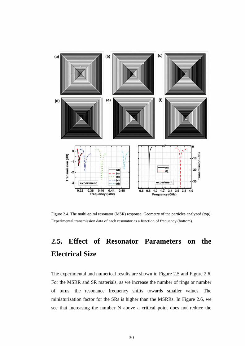
We introduced several splits to the SRs to increase the strength of the resonant
response. We fabricated six examples, which are shown in Figure 2.4. We
introduced one split to the SR particle with N = 20 and l = 8 mm, and changed
the position of the split as shown in Figures 2.4(a)-2.4(c). We increased the
number of the splits to 4, as shown in Figure 2.4(d). However, for these particles
the resonant strength was similar to the corresponding SR particle, and we did

29
not observe a significant increase in the resonance strength. We continued in this
fashion and obtained the particles as shown in Figures 2.4(e) and 2.4(f) for
which a much stronger resonance strength was obtained. The MSR shown in
Figure 2.4(f) is similar to MSRR shown in Figure 2.2(a) geometrically. In this
MSR structure, we had a split at every turn similar to the MSRR. As expected
the resonance frequency of this structure is almost the same as the MSRR with
the same l, N, s and w parameters. The shift at the resonance frequency of the
multi-spiral resonator that is shown in Figure 2.4(e) is acceptable and it
constitutes a good trade-off between the resonance strength and electrical size.
Its side length, l = 8 mm and resonance frequency, f0 = 0.81 GHz, electrical size,
u = λ0/30, and stop-band minimum is -27 dB. This particle is low profile and
easy to fabricate, and thereby it is a good candidate for metamaterial
applications.
30
Figure 2.4. The multi-spiral resonator (MSR) response. Geometry of the particles analyzed (top).
Experimental transmission data of each resonator as a function of frequency (bottom).
2.5. Effect of Resonator Parameters on the
Electrical Size
The experimental and numerical results are shown in Figure 2.5 and Figure 2.6.
For the MSRR and SR materials, as we increase the number of rings or number
of turns, the resonance frequency shifts towards smaller values. The
miniaturization factor for the SRs is higher than the MSRRs. In Figure 2.6, we
see that increasing the number N above a critical point does not reduce the

31
resonance frequency any more. The resonance frequency of the MSRR can be
significantly reduced up to 4-5 rings (N = 5). From Figure 2.6 we conclude that
it is not necessary to completely fill the inner part of the SR in order to obtain a
good reduction of the resonance frequency. Similar to the case of the MSRR, we
see that after some point, increasing the number N does not affect the resonance
frequency. The calculated electrical size (u), radius of the minimum sphere (a),
and resonance frequency (f0) for the optimum structures are shown in Table 2.1.
The reduction of the resonance frequency is comparable with the examples
found in the literature. The MNG materials are relatively easy to fabricate, low
profile and thereby can be packed into arrays in several dimensions. For the two
MSRR examples, we see that increasing the number of rings can reduce the
electrical size. This principle is also valid for the SRs. Moreover, using a higher
permittivity substrate will lead us to the further reduction of the resonance
frequency. These results can be explained by the aid of theoretical analysis and
modeling of the SRs in literature [39]. Moreover, a detailed analysis and circuit
model of our structures is given in Ref. [38].
Figure 2.5. Experimental transmission data as a function of the frequency (a) Multi split ring
resonators with the side length l = 8 mm. (b) Multi split ring resonators with the side length l = 5
mm. (c) Spiral resonators with the side length l = 8 mm.
The incident electromagnetic wave induces current on the resonators. At the
resonance frequency the electric and magnetic energy in the structure increases
dramatically. Since the structures are small compared to the wavelength, the
results can be explained by a quasi-static approach. We consider the change of

32
the total inductance (L) and capacitance (C) of the structures as the number of
rings or turns increases. The significant parameters to determine the L and C are
the average length of the strips and their filling ratio [38]. There are three
important results to be explained: the decrease of the resonance frequency,
miniaturization factor difference between the MSRR and SR structures, and the
saturation behavior.
Figure 2.6. Resonance frequency as a function of the number of rings and turns (Experiment and
simulation)
As N gets larger values the capacitance of the structures increases while the
inductance decreases. Since the proportion decrease of the inductance is smaller
than the proportion increase of the capacitance we observe a shift of the
resonance frequency to lower values. The proportion capacitance difference
between the MSRRs and SRs is due to the split capacitance of the MSRRs. The
total split capacitance of the MSRRs is significantly smaller than the distributed
one. Therefore, as we change the number of rings (turns), the proportion
capacitance change of the MSRRs and SRs shows a similar behavior. The

33
miniaturization factor difference of the MSRRs and SRs is related to inductance
[38]. For the MSRRs in addition to the average length of the strips, the filling
ratio has an additional decreasing effect on the inductance. Therefore, the
proportion decrease of the inductance is higher for the MSRRs that give a
smaller miniaturization factor. The saturation of the resonance frequency is due
to the saturation of both the inductance and the capacitance of the structures.
The average length and the filling ratio increase with a decreasing rate, which
yields a saturation behavior.
2.6. Substrate Effects and Size Scaling
We numerically studied the substrate effects on the design of electrically small
negative permeability medium particles. As shown in Figures. 2.7(a) and 2.7(d),
we selected the MSRR and SR resonators with l = 4 mm, and N = 10 for this
analysis. The resonance frequency and electrical size of the particles were
calculated for different substrates that are available in the standard printed
circuit board and optical lithography processes. In these calculations we ignored
the metallic and substrate losses, which do not have any significant effect on the
resonance frequency, but do on the simulation time. In Figures 2.7(b) and 2.7(c)
we plotted the resonance frequency in reduced units, i.e. we scaled the
frequency to the case in which Rogers RT/Duroid 5880 substrate was used. We
see that even though the substrate permittivity is a universal scale factor to first
order, the MSRR and SR cases do not overlap exactly in Figure 2.7. The root of
this difference is in the effect of the split capacitance of the MSRR. These
capacitances, in fact, sum up with the distributed capacitance between two
adjacent rings and do not have a counterpart in the SR case. In Figures 2.7(e)
and 2.7(f) we showed that increasing the substrate permittivity approx. 6 times
reduced the electrical size by approx. 2 times. Therefore, the miniaturization
factor can be improved by using higher permittivity substrates. In our
experiments, the substrate was RT/duroid 5880 with εr = 2.0 and we expect

34
higher miniaturization factors for different substrates, which are shown in Figure
2.7.
Figure 2.7. (a) Geometry of the multi-split ring resonator (MSRR) particle, N = 10, l = 4 mm, s =
w = g = 100 µm. (b), (e) Resonance frequency in reduced units (fred). For the MSRR fred = f0 /
(4.17), for SR fred = f0 / (1.307), where 4.17 and 1.307 are the resonance frequency for RT5880
substrate in GHz units, respectively. (d) Geometry of the spiral resonator (SR) particle, N = 10, l
= 4 mm, s = w = 100 µm. (c), (f) Calculated electrical size as a function of the substrate
permittivity. The permittivity of the substrates: RO5880: ε = 2.0, RO3003: ε = 3.0, FR-4: ε =
4.9, RO3006: ε = 6.15, RO3010: ε = 10.2, Si: ε = 11.9.
We finalize this section by searching the limits of the particles that can be
produced via the current printed circuit board technology. In Table 2.2, we
showed the measured resonance frequency of the MSRR and SR particles with
N = 20, l=20 s+w and the separation between the strips (s) and width of the
strips (w) were pushed simultaneously down to 50 µm. As the overall particle
size reduced the resonance frequency shifted to higher frequencies. By the size
scaling of composing individual particles many different combinations of media
with controllable permeability can be designed.

35
s = w (µm) 1
25
1
00
7
5
5
0 f0 (GHz) MSRR 1.26 1.55 2.03 3.09
SR - 0.31 0.41 0.60
Table 2.2. Geometric parameters and resonance frequencies for the particles (MSRRs and SRs)
with a number of rings (turns) N = 20 scaled to operate at higher frequencies. The side length (l),
strip width (w), separation between the strips (s), and resonance frequency (f0) are shown.
2.7. Tunability of Multi Split Resonators
One of the key advantages of the multi-split elements is that they can be tuned
by shorting the split-rings independently. We investigated the resonance of a
MSRR when one of the splits is closed at a time. Here we fabricated the
resonators as shorted. Figure 2.8 displays the results of digital tunability. As we
shorted the second outer most ring (Ring # 3) of the MSRR with N = 12, l = 8
mm, we saw that the resonance frequency shifts from 1.53 GHz to 2.17 GHz.
Measurements for the other cases shown in Figure 2.8 were also performed. It is
possible to short any arbitrary combination of splits, for the MSRR resonator
there are 211
combinations each of which will yield to a different resonance
frequency. One of the most suitable techniques for tuning multi-split elements is
to incorporate photo-switches at the split area of the rings. Photoconducting
switches for microwave applications were discussed by Vardaxoglou et al. [40].
In the presented technique a semiconductor substrate is placed or deposited to
cover the split area of the rings. When a light is focused on the split region the
photoconductor shorts the corresponding ring and the resonator starts to operate
at another frequency.

36
Figure 2.8. The shorted multi-split ring resonator (MSRR) response. Here the resonators were
fabricated as shorted and photoconductive switches were not used.
2.8. Temperature Dependent Resonator Response
In order to obtain metamaterials operating at higher frequencies, the physical
size of the metamaterial unit cells has to be smaller. In the process of unit cell
size scaling it was observed that due to the losses at the metallic components,
the magnetic resonance strength saturates [41]. In addition, the fabrication of
circularly shaped metallic resonators becomes more complicated as the
operation frequency increased [42, 43]. These obstacles led researchers to come
up with novel designs called planar metamaterials [6, 42-45]. Cut-wire pairs,
which provide magnetic resonance, had a smaller total capacitance compared to
the same size split ring resonator. Therefore, cut-wire based metamaterials can
operate at higher frequencies, which proposed a solution to the saturation and
fabrication problems [45]. The design and fabrication solutions provided in this
direction, especially to demonstrate negative index metamaterials at optical
frequencies, has attracted much attention [41, 46]. One critique should be
emphasized at this point: in order to be able to obtain an effective medium, the
electrical size of the composing elements should be at least an order of
magnitude smaller than the operation wavelength. The planar metamaterial

37
approach fails to provide this condition: the electrical size of the cut-wire pairs
were close to λ/2 and not much smaller than the operation wavelength. In the
present section, we would like to discuss another possible solution to the
weakening response of metamaterial elements. It is well known that the
properties of metallic features are strongly dependent on the environment
temperature [47]; surprisingly, there has been no direct observation of the low
temperature behavior of metamaterials that are composed of metallic elements.
We propose to decrease the operation temperature of the metamaterial elements,
which could be a candidate solution to the weak response of negative
permeability media.
We noticed very recently that: while trying to obtain deep subwavelength
magnetic metamaterial elements at microwave frequencies, due to the ohmic
losses of the constituting metallic elements with thin features, their magnetic
resonance saturates [32]. The saturation was directly related to the resistance and
electrical size of the resonators. Thereby, we expected that the reduction of
conductive losses would increase the resonance strength and thereby larger
negative permeability values could be obtained. In order to understand the
underlying physics, we selected a specific type of element, as shown in Figure
2.9, and investigated the theoretical formalism that is developed in the literature
[2, 7]. The effective permeability of a medium composed of periodically
arranged subwavelength resonators can be written as:
2
0
2
11
1eff
F
iQ
(2.1)
Here, F is the fractional volume constant, 0 is the resonance frequency,
is the frequency of the incident electromagnetic wave, and Q is the resonator
quality factor. The Q-factor related to the metal losses of the spiral resonators
(SR) as: 0c cQ L R . The Q-factor related to the dielectric losses ( dQ ) [48]
was found to be negligible and we used cQ Q . Whereas L is resonator

38
inductance, cR is the resistance associated with the metallic losses:
0c cR L vh . Here, c is the conductivity, h is the deposited metal thickness
and 2
c ne m . The free electron density is represented by n , e is the
magnitude of the electronic charge, is the mean free time, and m is the
electronic mass [47]. The temperature dependent quantity is the mean free time
. For copper, = 0.27 fs at 0°C and = 2.1 fs at the liquid nitrogen
temperature [48]. At lower temperatures the mean free path, conductivity, and
Q-factor increase in turn leading to larger negative effective permeability values.
In Figure 2.9, the electrically small element that was used as the unit cell of a
µ-negative medium is shown. Metallic features are obtained by etching the
deposited copper with a thickness of h = 9 µm coated on the RT/duroid substrate
with a thickness of t = 254 µm. The listed relative permittivity and dissipation
factor at 10 GHz are ε = 2.0 and tanδ = 0.0009. However, we used a slightly
different relative permittivity which was ε = 1.54. The parameters of the SR
elements are as follows: width of the strips, v = 100 µm; separation between the
strips, s = 100 µm; side length, l = 8.0 mm; and number of turns, N = 3.
Figure 2.9. The spiral resonator (SR) geometry: side length, l = 8.0 mm, width of the strips, v =
100 µm, separation between the strips, s = 100 µm, and number of turns, N = 3, thickness of the
substrate, t = 254 µm and deposited copper thickness, h = 9 µm.

39
The effective permittivity of the medium of densely packed resonators was
found to be [7]:
2
0
( 1 )(1 )
( )
y
eff
x z
p l K k
p p K k
(2.2)
Here, K denotes the complete elliptic integral of the first kind while
/ ( 2 )k s s v . The period in the x- y- and z- directions are denoted by xp , yp
and zp respectively. We assumed a closely packed medium with xp = 4.1 mm,
yp = zp = 8.2 mm. This formula is the low frequency permittivity of the
medium due to the inter-cell coupling of the resonators.
We observed that as we attempt to decrease the electrical size of the spiral
resonators by introducing more turns, the resonant strength obtained from the
transmission measurements reduced and saturated. When we changed the
resonator geometry by introducing splits on the rolled long metal thin strips, we
obtained higher resonance strengths. These studies led us to investigate the
effect of another parameter, temperature, which would increase the resonance
strength while keeping the element geometry and electrical size the same.
The temperature dependent resistivity of copper was given by the Mathissen
rule as [48] ( )tot res T . Here res denotes the residual resistivity that is
independent of temperature and ( )T is the resistivity for ideal lattice of the
material: ( ) (0) ( ) (0)T r T r . Here r is the reduced resistance:
( ) 1.056( / ) ( / )r T T F T , /T is the reduced temperature and is the
Debye temperature and = 347 K for copper. The values of ( / )F T between
the temperature range of interest were taken from resistivity tables given in Ref
[49]. By using the tabulated experimental data [48], we calculated res = 0.0151
µΩ.cm and (0)r = 0.7604. By using the specific formulas [38] we calculated the
capacitance, the inductance and Q-factor of our resonator and derived the

40
effective permeability and effective permittivity values for the temperature
range under interest. Note that instead of the formula given for the calculation of
effective substrate permittivity: 1 (2 )arctan( 2 ( ))( 1)sub
r t v s [38] we
used ε directly. In Figure 2.10, the enhancement of negative permeability for
lower temperatures can be clearly seen.
Figure 2.10. Theoretically calculated real part of the effective permeability of spiral resonator
based closely packed metamaterial medium. Data is shown for the selected temperature values.
As we obtained the permeability and permittivity values, the transmission and
reflection coefficients can be calculated by using the formalism developed for a
homogeneous slab. After the calculation of 21S amplitude, we commented on
the resonance strength. First, we found the effective index and impedance
values by using eff eff effn , eff eff effz . Then the transmission
amplitude was found by:
12
21
1cos( ) sin( )
2eff eff
i zS n kd n kd
z
(2.3)
Here, k is the wavevector, k c , and d is the slab thickness at the
propagation direction : zd p in our case. In Figure 2.11, we show the

41
temperature dependent 21S data. As we decreased the temperature, the
resonance strength increased in accordance with enhanced negative
permeability.
Figure 2.11. Theoretically calculated transmission amplitude data as a function of frequency.
The results are plotted with 23 K temperature steps.
To verify these theoretical results, we constructed an experiment setup and
investigated temperature dependence of resonance quality of the SR elements as
shown in Figure 2.12. The setup consists of two commonly grounded
microwave probe antennas, liquid nitrogen, a platinum resistance, and computer
controlled instruments: Agilent N5230A Vector Network Analyzer and an
Agilent AG34401 high performance digital multi-meter. The probe antennas
operate at the reactive near field regime. During the transmission measurement,
we placed a single element between the antennas wherein we obtained the

42
strongest response. The transmission spectra of free space i.e. before the element
was inserted, was used as calibration data. Instead of through calibration, we
used this method in order to clearly see the changes of the resonant response
during the experiment. When everything is placed, we pour the liquid nitrogen
into the can up to the antennas‟ level. The temperature of the sample was read
from the multi-meter by the aid of a platinum sensor, which was placed at the
same level as the sample. As the liquid nitrogen evaporates the temperature of
the sample increases and eventually reaches room temperature. The computer
aided automatic setup records the transmission response during the evaporation
process. The temperature dependent free space calibration data was obtained
similarly. We repeated the experiment for different samples and obtained their
temperature dependent calibrated transmission responses.
Figure 2.12. Experiment setup for temperature dependent resonator free space transmission
response.
In Figure 2.13 we show the transmission response of the SR at different
temperatures. Starting from the laboratory temperature, the transmission data
was shown down to 135 K in steps of 23 K. In this setup, since we kept the
antennas at a higher level than the liquid nitrogen as shown in Figure 2.12, the

43
lowest temperature value we obtained was around 125 K higher than the liquid
nitrogen temperature 77 K. We saw that the decreasing temperature did not have
any effect on the resonance frequency. On the other hand, due to the increased
conductivity, the resonance strength significantly increased. We also tested SRs
with N=4 and N=20. For the N=4 case the effect was minor and for the N=20
case we did not see any change. In order to be able to increase the resonance
strength of the samples with a longer metal length, we had to reduce the
temperature further, which was only possible with a cryogenic experimental
setup. In Figure 2.13, we showed the results of the obtained dip and peak values
at the resonance frequency as the temperature changed. For this particle, even its
electrical size kept the same, the resonant strength doubled by decreasing its
temperature 150 K. Doubling the resonance strength means larger negative
permeability values, or in other words the negative permeability values for
saturated elements at room temperature.

44
Figure. 2.13. Calibrated experimental transmission amplitude data as a function of frequency.
The results are plotted with 23 K temperature steps.
In principle, we can obtain a negative permeability medium by using
electrically small split-ring resonators under a low temperature environment at
optical frequencies. The mechanism works by decreasing the losses and not by
inhibiting the saturation of resonance frequency due to the kinetic energy of the
electrons in the metal. By using subwavelength elements together with wire
mesh at a low temperature, we can also obtain a negative index flat lens and
convey the current metrology to a higher level.

45
Chapter 3
Millimeter-Wave Scale Metamaterials
With Negative-Index of Refraction
3.1. Introduction
Most solid materials are in crystalline form, i.e. on the microscopic level the
ions are arranged in a periodic array [48]. In the presence of an applied
electromagnetic field, the materials‟ linear response is described by (electric)
permittivity (ε) and (magnetic) permeability (µ) parameters. By introducing an
artificial periodic array wherein repeated elements of the so-called metamaterial
are arranged, we can obtain a medium with a controllable linear response at any
desired narrow frequency band up to ultraviolet. The unit cells of metamaterials
are commonly composed of metallic-dielectric structures of several shapes [1, 2,
50]. Recently, ferroelectric and ferromagnetic materials were also utilized as
constituting elements leading to negative effective permeability media [51-54].
One can also obtain double negative medium by using all dielectric media at
microwave and optical regimes [55-58].
A medium of periodically arranged, subwavelength, high permittivity
ferroelectric rods was demonstrated to have effective negative permeability due
to the induced large displacement currents that create magnetic resonance in the
presence of the applied electromagnetic field at the GHz regime [51]. A
temperature tunable µ-negative medium, which operates at the first Mie
resonance mode of the constituting ferroelectric cubes, was observed between
13.65 - 19.65 GHz [52]. The properties of ferromagnetic materials have led to
novel opportunities for µ-negative medium designs. In the vicinity of
ferromagnetic resonance (FMR), the effective permeability of ferromagnetic

46
materials can be negative. This phenomenon was demonstrated experimentally
by using YIG slabs at 10 GHz [53] and (La:Sr)MnO3 layers at 90 GHz [54].
These are the few examples of metamaterials utilizing ferro-substances. A rather
widespread technique of realizing metamaterials involves nonmagnetic metal-
dielectric components.
Electrically small nonmagnetic metallic resonators are proposed as
constituting elements of a µ-negative medium [2] and metallic wire mesh
structures provide a low frequency plasma system with negative permittivity
[50]. An experimental demonstration of a double negative ( ε < 0, µ < 0 )
medium (DNG) as a superposition of split ring resonators (SRR) and wire mesh
medium was realized [1] and its unusual properties, such as negative index of
refraction, negative phase velocity, reversal of Cherenkov radiation, and
Doppler shift have attracted much attention. Applications of DNG and single
negative (SNG) media involve the electromagnetic phenomena of reflection,
absorption, radiation, cloaking, refraction, and subwavelength imaging. Planar
reflectors that operate like an artificial magnetic conductor (AMC) with high
surface impedance have been demonstrated at GHz frequencies [13, 14]. A
miniaturized rectangular patch antenna with a µ-negative medium substrate
operating at 250 MHz [7] as well as an electrically small circular patch antenna
loaded with a µ-negative medium are characterized experimentally and
theoretically [8]. A negative permeability medium element loaded monopole
antenna was demonstrated experimentally at around 4 GHz in terms of its
fundamental limitations [9] and multiple element effects [10]. A negative
permittivity shell loaded monopole antenna was developed analytically [11]. In
principle, one can enhance the transmission through a subwavelength aperture
by utilizing a µ-negative medium cover [12]. This topic was demonstrated
theoretically for the periodically arranged subwavelength holes by using deep
subwavelength resonators [59] in addition to the previous photonic crystal and
surface grating aided enhanced transmission studies [60-63]. By using a
metamaterial cover it is possible to nearly cloak a subwavelength object at a
particular frequency [20-22]. The negative refraction property of metamaterials

47
[1, 18] leads to a rather important application: the subwavelength imaging [64].
It is important to demonstrate a µ-negative medium at different regimes of
the electromagnetic spectrum. At the MHz region, µ-negative medium elements
lead to the improvement of magnetic resonance imaging by guiding the flux
from the object to the receiver [28]. Electrically small metallic elements on
planar substrates that operate at the MHz and GHz region and their potential
applications have been extensively studied theoretically and experimentally [24,
32, 65]. E-beam lithography techniques allow us to obtain single ring SRRs of a
110 nm side length [66]. By scaling the physical size of the SRRs, a magnetic
response at around 5 THz [5], 6 THz [67], 100 THz [46], and 370 THz [43]
were demonstrated experimentally. On the other hand, it has been extensively
studied that on the process of size scaling due to the ohmic losses of metallic
features, the magnetic resonance of SRRs saturate as the operation frequency
increases [41, 66, 68]. One way to overcome this problem was to introduce more
splits [69, 70] or by using cut-wire pairs [71] and thereby reducing the total
resonator capacitance. The resonant frequency increased via this method, but the
physical size remained the same. Therefore, the electrical size of the element
increased and became comparable to the operation wavelength. The realization
of an effective medium becomes a problematic issue as we increase the
electrical size of the constituting elements. Another method might be to decrease
the environment temperature to enhance the negative permeability [72]. In the
present work, we analyzed a split ring resonator based metamaterial medium
operating at the millimeter wave regime.
3.2. Design and Experiment
Our design was realized by utilizing the well developed printed circuit board
(PCB) technology. In Figure 3.1 we show the schematic view of the
manufactured metamaterial layers. On the front face, we have the split ring
resonators with parameters: width of the strips, w = 55 µm, separation between

48
the adjacent strips, s = 55 µm, split width, g = 55 µm, inner circle diameter, r =
110 µm. The period in the z- and y-direction are az = ay = 550 µm. In terms of
free space wavelength the period at the propagation direction (az) and one of the
lateral directions (ay) was approximately equal to λ0/6 at around the resonance
frequency. The substrate was Rogers RT/duroid 5880 with relative permittivity,
εr = 2.0 and loss tangent, tanδ = 0.0009. The thickness of the substrate was 250
µm and the deposited copper thickness was 9 µm. On the back face of the PCB,
we had continuous wires strips at a v = 275 µm width. The copper pattern
tolerance values (55 µm) were nearly at the edge of the current PCB technology.
For the slab characterization simulations we used a linearly polarized plane
wave propagating at the –z- direction is incident upon the metamaterial layers,
the E-field is at the y- direction and the H- field is at the x- direction. In these
simulations we used the CST Microwave Studio [37]. The unit cell of the
metamaterial medium under test is inserted into the simulation domain with
periodic boundary conditions at the lateral directions (y- and x- directions). We
simulated the reflected and transmitted time signals obtained the relevant
complex S-parameters.
Figure 3.1. The parameters of the composite metamaterial medium (CMM).
The experiments were performed by using a millimeter-wave network
analyzer with a 50 dB dynamic range from 75 GHz to 115 GHz. The
transmission data in air was obtained by the aid of two standard gain horn
antennae. The orientation of and distance between the antennae were kept fixed
during the experiments. The media have 30 × 45 number of unit cells along the
x- and y- directions, and the number of unit cells along the propagation direction

49
was varied as 3, 5, 7, and 9. The space between the metamaterial layers at the x-
direction was 254 µm. We inserted the metamaterial slab between the horn
antennae and measured its transmission response, and then removed the slab and
noted the calibration data. By measuring the transmission response of the four
different media, we characterized the composite metamaterial medium based on
the qualitative effective medium theory [73, 74].
3.3. Transmission Based Qualitative Effective
Medium Theory Analysis
In the effective medium theory analysis, we considered the transmission
response of four different unit cell structures and concluded whether the
composite metamaterial medium (CMM) was double negative. The SRR and
closed ring resonator (CRR) geometry and corresponding induced surface
current at the resonance frequency are all shown in Figure 3.2(a) and 3.2(b).
Mostly due to the distributed capacitance between the two rings of the SRR, we
observed induced circulating currents and a magnetic dipole-like response. By
shorting the gaps of the SRR, we introduced the CRR structure on which the
circulating currents disappear and at the operation frequency CRR acts like an
electric dipole. In Figure 3.3, we showed the transmission spectra of the SRR
and CRR media. There were 3 unit cells at the propagation direction. The media
were transparent up to 75 GHz (not shown) and a stop-band for the SRR-only
medium was observed. This gap was not present at the CRR transmission data,
indicating its magnetic origin. Next, we considered the ε-negative wire-mesh
medium. Its plasma frequency was designed to be at around 200 GHz. Even the
wire-only medium might have negative-ε below the plasma frequency, the
composite metamaterial acts as a different plasmonic system. The SRRs of the
composite metamaterial kick in the effective permittivity and cause a downward
shift of the wire-only medium plasma frequency. Therefore, instead of just
considering the wire-only medium transmission response, we should also take

50
into account the transmission response of the CRR and wire composite
(CCMM). We designed the medium parameters in such a way that the plasma
frequency of the CCMM was around 150 GHz. We can guarantee thereby that
the CMM medium is ε-negative below 150 GHz. Finally, we concluded that the
transmission peak at around 100 GHz, as shown in Figure 3.3, was due to the
double negative nature of the CMM medium. Our simulation and experimental
results are in good agreement and we would like to emphasize that the
experiment data is the average of many reproducible measurements. As
expected, the transmission peak value ~ -2.5 dB was lower than the ideal
simulation result. On the other hand, by using a low loss substrate and rather
thick metal coating, we improved the ~ -25 dB transmission peak value of our
group‟s previous 100 GHz metamaterial demonstration [4]. Moreover, instead of
photolithography techniques, we achieved the desired double negative properties
at the millimeter-wave regime by using a rather cheap technology. At the
production step we stacked 30 planar layers of the medium under test in order to
cover the entire incident beam. For the SRR-based metamaterial medium, the
transmission response was not very sensitive to the angle between the antenna
emission direction and metamaterial slab normal [75], or to the small
misalignment of the layers [76]. This was not the case for the planar
metamaterial media such as the fishnet structure [3].
Figure 3.2. The schematic view and surface current (a) SRR. (b) shorted SRR, i.e. closed ring
resonator (CRR).

51
Figure 3.3. Transmission spectrum for 3 layered metamaterials in the propagation direction.
Response of the SRR, CRR, CMM and shorted CMM i.e. closed composite metamaterial
(CCMM) are shown. (a) simulation (b) experiment.
3.4. Retrieval Analysis
Another well-developed characterization method of metamaterials is the
standard retrieval procedure [77-79]. The assigned effective refractive index (n)
and relative impedance (z) values of the metamaterial slab can be extracted by
using the complex scattering parameters with respect to 50 Ω. If the
metamaterial slab under test is symmetric with respect to the x-y plane, i.e. S11 =
S22 and S21 = S12, we can extract the effective medium parameters (n, z) of the
metamaterial by using the terminology that was developed for the homogenous

52
slab. By using ε = n z, and µ = n / z formula, we derive the effective permittivity
and permeability of the media. The complex scattering parameters for the case
of our metamaterial were obtained from the simulations and by using the
formalism of Refs. [77-79]. We extracted the n, z; ε, µ parameters of the CMM
medium and showed as Figure 3.4. It is clear that at around 100 GHz the CMM
medium is double negative.
At this point we would like to emphasize that just by itself the pass-band
region shown in the qualitative effective medium theory can‟t be claimed to be
double negative. Either the complete transmission analysis of the four structures
should be studied or the pass-band region should be supported by the retrieval
analysis. Here, we demonstrated the correlation between the two independent
well developed effective medium theory analyses: the retrieval and transmission
based effective medium theory.

53
Figure 3.4. Extracted parameters as a function of frequency for the SRR-based metamaterial
medium. (a) Refractive index (b) Impedance (c) Permeability (d) Permittivity
3.5. Loss and Bandwidth Analysis
The resonant nature leads the narrow bandwidth of metamaterials. We calculate
the fractional bandwidth of the negative region via FBW = Δf / f0, where Δf is
the half power bandwidth and f0 is the center frequency. We obtained for the 3
layer case Δf = 4.8 GHz, f0 = 99.9 GHz and FBW = 4.8 %.

54
Figure 3.5. Transmission spectra in the linear scale for a several number of CMM layers in the
propagation direction. (a) Simulations (b) Experiments.
In Figure 3.5 we show the effect of increasing the number of layers at the
propagation direction to the transmission response. As expected the total loss
(dB/mm) increases as the number of layers increase. We summarized the
resulting loss and bandwidth data at 100 GHz in Table 3.1. We can clearly state
that as we increase the number of metamaterial layers at the propagation
direction, the total loss increases and the FBW decreases.
Number of Layers 3 5 7 9
Loss ( dB / mm ) 2.1 2.8 2.9 2.2
FBW( % ) 7.5 5 3.9 3.3
Table 3.1. Calculated loss and FBW parameters for the increased number of metamaterial layers
in the propagation direction.
3.6. Direct Observation of Negative Refraction
The schematic of the refraction spectra measurement setup is shown in Figure
3.6(a). The setup consists of a millimeter-wave network analyzer, automated

55
linear translation system, and two horn antennas as the transmitter and receiver.
There were five metamaterial layers at the propagation direction. The transmitter
horn antenna was on the right-hand side of the metamaterial with respect to its
central axis. We scanned the spatial intensity distribution along the second
metamaterial-air interface from 75 to 115 GHz. In Figure 3.6(b) we made an
additional analysis related to anisotropy, in order to clarify that this anisotropic
metamaterial has a negative index that indeed leads to the negative beam shift.
In this analysis, we used the retrieval formalism developed in Ref. [79], which
takes into account the asymmetry of the medium at the propagation direction.
Even though the method of Ref. [79] was developed by considering a
homogeneous media, it can be used to retrieve the effective medium parameters
of anisotropic multi-dimensional metamaterials [79]. From the complex
scattering parameters we extracted the metamaterial‟s refractive index and as
shown in Figure. 3.6(b), we demonstrated that for oblique incidence with angle
used in the experiment (22°) the metamaterial have a negative index of
refraction at around 100 GHz. The refractive index, n was -1.0 at 99 GHz.
Recently an experimental proof on the insensitivity of SRR-based metamaterials
to the angle of incidence was provided. They are in parallel with the analyses‟
results given here [80].

56
Figure 3.6. (a) Beam shifting experiment geometry, (b) Retrieved effective refractive index for
the oblique incidence for α = 22°.
Figure 3.7 shows the transmission spectra as a function of frequency, in
which the lateral position for the angle of incidence was α = 22°. For control
purposes, we also measured the free space response. It is evident that for the
metamaterial case, the transmitted beam appeared on the right-hand side.
Thereby, the index of refraction of the metamaterial medium was negative. The
frequency cuts at 99 GHz are shown in Figure 3.8, in which the appearance of a
negatively refracted beam can be seen more clearly. By using the Snell‟s Law of
refraction, we determined the refractive index from the experiment. The
parameters shown in Figure 3.6(a) are as follows: thickness of the slab was d =
2.75 mm, distance of the horn antenna to the interface was d0 = 1 mm, measured
shift distance was x = 0.6 mm, and the incidence angle was α = 22°. By using
simple geometric equations and Snell‟s Law: sin sin( )air NIMn n ,
1 tanx d , 2 0 tanx d , 1 2x x x , we derived the other parameters:
refraction angle, 20 , shift distances, 1 1.0x mm, 2 0.4x mm and
refractive index, n = -1.0. The results are in good agreement with the theoretical

57
calculations. By just looking at the beam-shift we can‟t claim that the medium
has a negative index. Thereby, here we demonstrated that there is a correlation
between the negative band region determined by the qualitative effective
medium theory analysis, retrieval analysis and the beam shifting experiment. We
do not expect such a frequency dependent response from an arbitrary anisotropic
medium.
Figure 3.7. Transmission spectra as a function of frequency and scanning distance (a) Free-space
(b) Negative-index metamaterial.

58
Figure 3.8. Frequency cuts at 99 GHz. (a) Experiment: free-space (solid curve), negative index
metamaterial (NIM) (dashed curve) (b) Drude-Lorentz simulations.
We also confirmed the experimental results by using CST simulations. In
these simulations, we modeled our negative index medium with the isotropic
Drude-Lorentz model. The Drude model formula was:
2( ) p ci with the parameters: the plasma frequency,
2 130p GHz, the collision frequency, 0.01c Hz. For the magnetic
dispersion Lorentz model formula was:
2 2 2
0 0( ) s i (3.1)
with the parameters permeability infinity, µ∞ = 1, permeability static, µs = 1.07,
resonance frequency, 0 2 97.9 GHz and the damping frequency, γ = 1.3
GHz were used. The Drude-Lorentz model parameters were selected in such a
way that they were in good agreement with the retrieved effective parameters of
the metamaterial medium at around 99 GHz. We made a Drude-Lorentz model
fit to the retrieved effective medium parameters: permittivity (ε) and
permeability (µ) and selected the model parameters by specifically paying
attention to 99 GHz. We applied perfect electric conductor boundary conditions

59
at the vertical direction (y) and perfect absorbing boundary conditions in other
directions. The transmitter horn antenna model that was used in the simulations
has the same physical parameters as the one used in the experiments. It was fed
with a waveguide port. By this method, the field propagation and far field
profiles were simulated with efficient computation power. We demonstrated the
field profile of the experiment in Figure 3.9 as an animation. The appearance of
the beam on the right-hand side of the second interface, negative phase velocity
inside the metamaterial medium, negative refraction and the reflection properties
can all be seen in this animation. In Figure 3.9 instead of simulating the actual
slab composed of many metamaterial unit cells, we used a homogeneous
medium with assigned index and impedance. By this method, we could be able
to observe the field profile in and around the negative index metamaterial slab.
The main advantage of this method was the reduction of required computer
power and memory.
Figure 3.9. Electric field magnitude in y- direction at 99 GHz.
3.7. Study of a Metamaterial Prism
We synthesized a prism shaped metamaterial that was composed of stacked 7
layered blocks, in the lateral (x) direction. There were six different block types
with unit cells in the propagation direction ranging from 3 to 9, as shown in

60
Figure 3.10. The angle between the prism‟s second interface and propagation
vector was α = 8.4°. The setup consisted of a millimeter-wave network analyzer,
an automated rotary scanner system, and two horn antennas as the transmitter
and receiver. The transmitter horn antenna was parallel to the first meta-prism
interface. We scanned the angular transmission intensity at a distance of R = 38
mm, which corresponded to the far field of the antennas from 75 to 115 GHz.
Figure 3.11 shows the transmission spectra as a function of the frequency and
scanning angle. As the frequency increases, the beam refracts from the negative
to positive side. The transition can be seen from a negative index to positive
index in Figure 3.11. We would like to point out the frequency band at which
the beam was refracted to the negative side coincides with double-negative
region predicted by the effective medium analyses. The unit cells of the
metamaterial under study were adequately electrically small so that the
periodicity related effects were minor.
Figure 3.10. Schematic of the setup used in the millimeter-wave metamaterial prism experiment.
The metamaterial sample, source and detector antennas, and air-prism second interface normal
are shown. The prism angle α = 8.4° and scanning angle θ were changed from -60° to 60°.

61
Figure 3.11. The transmission spectra as a function of the frequency and scanning angle θ.
In Figure 3.12, we showed the frequency cuts that were taken from the
experimental data at 100 GHz. The normal of the second interface was
demonstrated with a blue dashed line and arrow. We can compare the results of
the free space and meta-prism cases in this figure. A negatively refracted beam
emerges on the left-hand side of the prism normal, whereas the beam emerged
on the right-hand side for the positive index medium. We also confirmed the
experimental results by using CST simulations, in which the negative index
prism was modeled with the Lorentz-Drude dispersion theory. The Drude-model
parameters were as follows: the plasma frequency was equal to, ωp = 2 π 130
GHz, the collision frequency was equal to, υc = 0.01 Hz. For the magnetic
dispersion, the following Lorentz-model parameters were used: permeability at
infinity was equal to, µ∞ = 1, permeability static was µs = 1.07, resonance
frequency was ωres = 2 π 97.9 GHz and the damping frequency was γ = 1.3 GHz.
The retrieved parameters of the metamaterial medium were taken into account
when determining the Drude-Lorentz model parameters. At around the
frequency of interest, the retrieved ε and µ values were as close as possible to
the Drude-Lorentz values. In this simulation, we applied the perfect electric
conductor boundary conditions at the vertical direction (y) and in the other
directions the perfect absorbing boundary conditions were applied. The physical

62
parameters of the transmitter horn antenna used in the simulations were the same
as the experimental configuration except a waveguide port was placed instead of
a coaxial probe feed. By this method, we obtained the field propagation and far
field profiles with affordable computation power in a reasonable amount of time.
Figure 3.13 shows the field profile. The negatively refracted beam emerging
from the second prism interface, the negative phase velocity inside the
metamaterial medium, as well as the reflection properties can be seen in this
figure and corresponding animation.
Figure 3.12. Frequency cuts of the transmission spectra at 100 GHz for the free-space and meta-
prism (a) experiments (b) simulations.

63
Figure 3.13. Two dimensional map of the electric field amplitude at the y-direction. Negative
refraction and negative phase velocity can be seen.
3.8. Far Field Radiation Behavior of Horn
Antenna and Metamaterial Composite
In this part, we investigated a novel composite antenna, which has two parts: i)
horn antenna, ii) double negative metamaterial lens. Figure 3.14 displays
measured and calculated far field pattern of the metamaterial lens/ horn antenna
composite structure. We have modeled the homogeneous metamaterial by using
Drude-Lorentz model in a way that at the frequency of interest the retrieved ε
and µ values almost coincide. Other parameters in the simulations are kept the
same as experiment. At the far field, R = 38 mm, by implementing an automated
experiment setup we scanned the field intensity for both the horn antenna and
for the hybrid structure. Being in good agreement the simulation, the
experimental results showed that the metamaterial lens decreases the angular
width of the hybrid structure‟s radiation pattern at the E-plane. Due to the
experimental limitations we couldn‟t be able to scan the less interesting H-plane
and couldn‟t comment on the directivity, gain and efficiency of the hybrid
structure. We observed that the maximum transmitted peak value was 2-3 dB
less than the horn-only case due to the lossy nature of the metamaterial lens. The
behavior of the hybrid structure composed of a horn antenna as driven element

64
and DNG material as director can be considered as a novel phenomenon, which
is similar to the behavior of Yagi-Uda antenna. The DNG part is passive and
thin. It forms a rough image of the source. Its rough image and source itself can
be used to explain the higher directivity of the composite system. In our
millimeter-wave setup, we could only use horn antennas as the source and sink.
Thereby we haven‟t tried to observe or optimize this effect with different
sources. Moreover, the number of DNG materials at the propagation direction
couldn‟t be increased due to our fabrication and measurement limitations. On
the other hand, in Figure 3.14 (d) we showed the numerical result for the case of
two DNG materials at the propagation direction. We showed that the directivity
further increased in this case. The separation between the DNG materials was
equal to their thicknesses and neither the thicknesses nor the separation between
them was optimized. Here, we prefer to qualitatively demonstrate and explain
the observed phenomenon.

65
Figure 3.14. Simulated field map of (a) horn antenna, (c) horn antenna and metamaterial lens
(hybrid structure) at 99 GHz. Focusing and redistribution of waves can be seen in part b. Far
field patterns (b) horn antenna (d) hybrid structures with 1 and 2 NIM slabs at the propagation
direction.

66
Chapter 4
Planar Metamaterials
4.1. Introduction
One of the major aims of the study of metamaterials is to achieve negative
refraction at the visible range of the electromagnetic spectrum. By scaling the
size of the SRR, a magnetic response at around 1 THz [81], 6 THz [67], 70 THz
[82], 100 THz [46], and 200 THz [43] is achieved experimentally. However,
metamaterials that are composed of layers of SRRs and wires have several
restrictions. Firstly, as the size of the SRR is decreased, the magnetic resonance
becomes weaker and approaches a limit [66]. A large number of SRR layers has
to be produced and stacked in order to obtain the negative index medium. The
fabrication of SRRs with resonance frequency at the visible range is rather
difficult. Moreover, the alignment of the produced layers is a major problem.
The restrictions of the conventional metamaterial construction are overcome by
way of the introduction of planar metamaterials [43, 45, 66, 83].
Metamaterials for which the propagation direction is normal to the plane of
the metamaterial layers are called planar metamaterials. A negative index
metamaterial is experimentally demonstrated at 150 THz by using a pair of
metal layers that are separated by a dielectric in order to provide resonant
interactions along with a periodic array of holes [83] and at 200 THz by using a
thin layer of pairs of parallel metal nanorods [84]. At this point, it is noteworthy
that the imaginary part of the effective index of refraction for these works at the
operation frequency was large, and thereby, the losses were significant. The
systematic study and characterization of cut-wire pairs (cwp) operating at 300

67
THz [45] and the fishnet design at 200 THz [6] were performed experimentally.
In the fishnet design, the cut-wire pairs are as wide as the lattice constant and are
physically connected with the continuous wires, see Figure 4.1. Recently, a
negative index metamaterial operating at 385 THz was experimentally
demonstrated by using the fishnet design [42].
The experimental characterization and parametric study of planar
metamaterials is rather easy for the operation frequencies at the GHz range. One
advantage of working at this frequency regime is that the metamaterial features
are sufficiently large to study several effects, such as the misalignment of metal
pairs and metamaterial layers. Such studies are rather difficult to perform at the
THz range. Recently, planar metamaterials at 14 GHz attained by using cut-wire
pairs [85, 86], and at 13 GHz by using the fishnet design [87], were
demonstrated experimentally. In the present work, we extend the experimental
and numerical study of the fishnet structure to the case in which the structure is
symmetric with respect to the x-y plane, which is shown in Figure 4.1. In this
case, the x- and y-polarized incident wave the structure gives the same response.

68
Figure 4.1. The geometry of one unit cell of the fishnet metamaterial. The electromagnetic wave
propagates in the –z direction, in which E and B are along the y and z directions. There are two
layers in the propagation direction; the parameters are given in the text.
4.2. Current Distribution, Transmission and
Retrieval Analyses for 20 GHz
Theoretical modeling of the metamaterials is performed by using effective
inductor-capacitor circuits (LC circuit). When the elements of the metamaterial
in the propagation direction are small compared to the free space wavelength at
the operation frequency, we can use the quasi-static process approach [30]. An
LC circuit model for the fishnet structure was given in Ref. [87]. The model
predicts the dependence of magnetic resonance frequency on the structure‟s
parameters by way of the formula:
x
mall
w
lf
21
2
2
1
1 (4.1)

69
where 2
1
2
lal
y , 1l is the cut-wire length, 2w is the wire width, xa and
ya are the periodicity in the x and y directions, see Figure 4.1.
There are two methods for the characterization of metamaterial slabs: the
retrieval procedure and the effective medium analysis. The retrieval of the
effective index of refraction (n), impedance (z), permittivity (ε), and
permeability (µ) of a metamaterial slab is extracted from the magnitude and
phase of the reflection and transmission data [77, 78]. On the other hand, the
effective medium analysis is performed by only using the magnitude of the
transmission data. However, four different structures are necessary: µ-negative
(MNG) material, shorted MNG material, composite medium of MNG materials,
and continuous wires (CMM), as well as the shorted CMM [74]. In the present
chapter, we followed the latter characterization method, in which our MNG
material is the cut-wire pairs, Figure 4.2(a), and the CMM is the fishnet
structure, Figure 4.3(a).

70
Figure 4.2. The geometry and surface current (a) the cut-wire pair (cwp). (b) shorted cut-wire
pair (c) Transmission spectrum magnitude of the cwp and shorted cwp structures.
We perform a qualitative effective medium theory characterization
numerically via the commercial software CST Microwave Studio. In the
simulations, we insert the unit cell of the structure in a waveguide and obtain the
scattering parameters by using waveguide ports. By way of this method, the
structure unit cell is assumed to extend to infinity in the lateral directions and the
incident, reflected and transmitted waves are in the form of a plane wave. The E
field is in the y-direction, the B field is in the x-direction, and the propagation
vector is in the negative z-direction: yE ˆˆ , xH ˆˆ , zk ˆˆ . The metallic

71
features are assumed to be a perfect electric conductor (PEC) and the relative
permittivity of the substrate is εr = 1.94. Other structure parameters are as
follows, see Figure 1: ax = ay = 10 mm, az = 3 mm, l1 = w2 = 5 mm, t1 = 1 mm, t2
= 0.05 mm. We have one layer of the metamaterial in the propagation direction,
in which the metal and substrate losses are ignored. The results of the first part
of the effective medium analysis are summarized in Figure 4.2.
For the case of metamaterials a stop band at the transmission spectra
indicates a resonance phenomenon, which could be electrically or magnetically
originated. The fishnet metamaterial is composed of metallic and dielectric parts
both of which are nonmagnetic. The only source of magnetic resonance is the
circulating currents driven by the capacitance between the cut wires. A simple
method to determine whether a stop band is due to the magnetic or electric
resonance is to shorten the cut wire capacitance as shown in Figure 4.2(b). By
this way the driven force of the circulating currents will be eliminated and the
magnetically originated stop band at the transmission spectra will disappear,
Figure 4.2(c) [74]. Moreover, as we kill the magnetic resonance by shorting the
cut-wire pairs the circulating surface current in Figure 4.2(a) disappears and the
current pattern becomes similar to an electric dipole, Figure 4.2(b). The second
part of the effective medium theory analysis is summarized in Figure 4.3. The
geometry of the CMM and shorted CMM are shown in Figure 4.3(a) and Figure
4.3(c), respectively. In this part, there are two layers in the propagation
direction. The transmission data implies the existence of a negative index of
refraction at around 21 GHz. However, the magnetic resonance frequency of the
cut-wire pairs was around 19.5 GHz. This difference is a characteristic of the
fishnet metamaterial and can be explained by considering the surface current at
the first face of the metamaterial, Figure 4.3(b). When we combine the cut-wire
pairs with the continuous wires, the effective cut-wire length decreases and the
magnetic resonance frequency increases. Finally, we would like to note that the
transmission properties remain the same when the incident wave polarization is

72
rotated 90°. Since the structure is symmetric with respect to the yx plane
this behavior was expected.
Figure 4.3. Schematic view (a) two layer CMM (c) two layer shorted CMM. Surface current on
the face of the first layer (b) CMM (d) shorted CMM. (e) Magnitude of the transmission data for
the CMM and shorted CMM structures.
The experiments were performed via an HP8510C Network Analyzer and two
standard gain horn antennae. After the full two port calibration we first measured
the scattering parameters for the free space i.e. without the metamaterial layers
being inserted. Subsequently, we repeat the experiment wherein the metamaterial

73
slab is in between the antennae. The distance between the transmitter and receiver
antennae is kept fixed at 79 mm during the experiments. The metamaterial
substrate is cardboard of 1 mm thickness and the metallic features are formed by
using an aluminum based tape. In Figure 4.4 the transmission magnitude and
phase data are shown. The transmission data is scaled to the free space data. The
experimental results are in good agreement with the simulation. At this point we
should clarify the difference between the design simulations shown in Figure
4.3(e) and the more realistic simulation shown in Figure 4.4(a). In the design
simulations, we assumed lossless metal and dielectric parts in order to clearly
demonstrate the effective medium theory concepts (see Figure 4.2(c) and Figure
4.3(e)). In Figure 4.4(a), when comparing the simulation and experimental results
we have taken the loss effects into account. The conductivity of the aluminum
type and dielectric were 20000 S/m and 0.001 S/m respectively. The possible
reasons of the discrepancies between the simulation and experiment are: the
misalignment of the continuous and cut-wire pairs in a layer, small deviations of
the fabricated material parameters from the intended values and misalignment of
the multiple layers. We expect the transmission band between the frequencies
20.2 and 21.2 is negative (see Figure 4.3(e) and Figure 4.4(a)). The fractional
bandwidth of the negative region is narrow and calculated as 2% by using the
formula: FBW = Δf/f0, where is Δf is the half power bandwidth and f0 is the
center frequency. The effective medium theory is a qualitative approach and in
order to determine the negative band exactly a robust retrieval analysis is
necessary [77, 78]. In Figure 4.4(b) we demonstrate that the phase shift of the
wave within the left handed band is negative. In this band, as the number of
layers increase, the phase decreases.

74
Figure 4.4. (a) The transmission spectrum of the fishnet metamaterial simulation and
experiment. In the simulation, the loss of the metal and dielectric parts is taken into account. (b)
Phase spectra of the metamaterial for a different number of layers.
4.3. 100 GHz Fishnet Metamaterial Design
The front view photograph of the fishnet metamaterial and unit cell are shown in
Figure 4.5. There are 14 unit cells at the lateral directions, the incident E-field is
in the y-direction, the B-field is in the x-direction and the propagation vector is
in the –z-direction. The period in the x- and y-direction are ax = ay = 2 mm, cut-
wire pair length is l = 1 mm and wire width is w = 1 mm. The relative
permittivity of the substrate is εr = 2.2 + i 0.0009 and the substrate thickness is
254 µm. The coated copper thickness and conductivity are 9 µm and 5.8 x 10⁷
S/m, respectively.

75
Figure 4.5. (a) A front view photograph of the fabricated fishnet metamaterial layer. The
electromagnetic wave propagates in the –z direction, in which the E-field and B-field are along
the y and z directions. (b) The geometry of one unit cell of the fishnet metamaterial.
4.4. Current Distribution, Transmission and
Retrieval Analyses for 100 GHz
The results of the qualitative effective medium theory are shown in Figures 4.6
and 4.7. The electrically small cut-wire pair resonator geometry and induced
surface current at the resonant frequency are shown in Figure 4.6(a). The
circulating currents that are driven by the capacitance between the cut wires
resemble a magnetic dipole response. When we short the capacitance, as shown
Figure. 4.6(b), the circulating currents disappear and the response becomes
similar to an electric dipole. The corresponding effect on the transmission
spectra is the disappearance of the stop band, as shown in Figure 4.7(a). We can
thereby infer merely by considering of the transmission spectra as to whether the
stop band was magnetically originated. In Figures 4.6(c) and 4.6(d) we exhibit
the fishnet metamaterial unit cell and its shorted version. The fishnet
metamaterial is composed of cut-wire pairs that are connected to long
continuous wires along the vertical (y) direction. The long continuous wires act
as a low frequency plasmon system with a plasma frequency that is larger than
the metamaterial operation frequency. The plasma response of the fishnet
structure is expected to be very similar to the shorted version. Therefore, from

76
the transmission data show in Figure 4.7(b) we infer that the medium is ε-
negative for f < 120 GHz and the transmission peak at ~100 GHz is the result of
the double negative nature of the fishnet metamaterial.

77
Figure 4.6. The schematic view and surface current (a) the cut-wire pair (cwp). (b) shorted cut-
wire pair (sh-cwp) (c) fishnet (fn) (d) shorted-fishnet (sh-fn).

78
Figure 4.7. Transmission spectrum magnitude for one layer of structures at the propagation
direction (a) the cut-wire pair (cwp) and its shorted version. (b) fishnet (fn), shorted fishnet (sh-
fn) and the wire mesh medium.
We also present the standard retrieval analysis results. By using the complex
scattering parameters we extract the index and impedance of the one layer
fishnet metamaterial. The real part of the refractive index, permeability and
permittivity are negative at around the transmission peak, Figure 4.8. The
resonant nature leads to the narrow bandwidth of metamaterials. The fractional
bandwidth of the negative region is calculated via FBW = Δf / f0 , where Δf is
the half power bandwidth and f0 is the center frequency. Here we obtain Δf =
1.57 GHz, f0 = 97.7 GHz and FBW is 1.6%, which is a typical value for a fishnet
medium [44]. We would like to emphasize that for any arbitrary polarization of
the plane perpendicular incident wave the response of the metamaterial is the
same because the unit cell of the fishnet metamaterial is symmetric with respect
to the x-z and y-z planes.

79
Figure 4.8. Extracted parameters as a function of frequency for the fishnet metamaterial
medium.
For the experimental demonstration we use a millimeter-wave network
analyzer that has a 50 dB dynamic range at the 75-115 GHz band. The
experiments are performed in free space and room temperature by using two
standard gain horn antennae. We kept the distance between (16 mm) and
orientation of the antennae fixed and used the free space transmission data as
calibration data. We stacked several layers at the propagation direction with a
layer to layer separation of 250 µm. Spacers are placed at the very edges of the
metamaterial layers so that the medium between the layers is air. In Figure 4.9
the experiment and corresponding simulation data are shown. We see a narrow
transmission band at around 100 GHz. The experiment and simulation results
are in good agreement in terms of the operation frequencies; however, the
transmission magnitude in the experiment is rather low. At this point we would
like to investigate the possible reasons for the discrepancies between the
experiment and simulations in two groups: the fabrication based and alignment

80
based discrepancies. At the fabrication step, there may be small deviations of the
material parameters from the intended values in terms of the size of the metallic
features and misalignment of the features at the front and back faces of the
substrate. However, our fabrication is a very well controlled process wherein the
accuracy of the feature size is less than a micron. Therefore, we do not expect
any significant fabrication based discrepancies. On the other hand, as the
operation frequency increases the alignment of the several stacked layers and
keeping the angle between the antenna emission normal and metamaterial plane
normal as zero becomes rather difficult.
Figure 4.9. Transmission spectra in linear scale for several number of fishnet layers in the
propagation direction. (a) simulations (b) experiments

81
Chapter 5
Oblique Response of Flat
Metamaterial Slabs
5.1. Introduction
Metal dielectric based metamaterials are demonstrated to operate for normal
incidence at several regimes of the electromagnetic spectrum. Some recent
designs increased the operation frequency but at the expense of effective
medium concepts. They used elements of electrical size that are comparable to
the operation wavelength [42]. In order to be able apply the effective medium
characterization methods to the designed metamaterials several points should be
kept in mind. Firstly, the electrical size of the resonators are to be at least an
order of smaller than the operation wavelength. Secondly, the number of
metamaterial layers at the propagation direction should be large enough that the
parameters permeability and permittivity are meaningful. Thirdly, the
metamaterial should have an invariant response for oblique incidence especially
for the exciting applications such as subwavelength imaging and the focusing of
light.
In the present chapter, we first focused on the response of a split-ring
resonator based composite metamaterials. The results are presented at the S-
band for the case when the incident beam has a nonzero incidence angle. First,
we introduced our design and structure parameters, and then showed the results
of the qualitative effective medium theory characterization method. The
frequency dependent response of a three-layered composite metamaterial, which

82
was illuminated with an oblique angle with respect to two bases, will be shown
experimentally. Then, the results will be compared with a five-layered case.
5.2. Transmission Based Qualitative Effective
Medium Theory of A SRR Based Metamaterial
The electrically small resonator part of the designed unit cell is shown in Figure
5.1. At the microwave frequencies, we prefer to utilize the printed circuit board
technology for the fabrication of the metamaterial samples. By etching the metal
coated substrates as desired, split ring resonator (SRR) shapes were obtained
with following parameters: the strip width, w = 0.9 mm, the separation between
the adjacent strips, s = 0.2 mm, the split width, g = 0.2 mm, outer ring radius, r1
= 3.6 mm, inner ring radius, r2 = 2.5 mm. The period of the resonators at the y
and z directions was l = 8.8 mm. The substrate was FR-4 with relative
permittivity, ε = 3.75, and the dissipation factor, tanδ = 0.002. The thickness of
the substrate was 1.6 mm and the deposited copper thickness was 30 µm. On the
back side of the substrate, centered continuous wires were fabricated with a
width of w = 0.9 mm.
Figure 5.1. (a) The negative permeability medium unit cell: split ring resonator with parameters,
w = 0.9 mm, s = 0.2 mm, g = 0.2 mm, r1 = 3.6 mm, r2 = 2.5 mm, l = 8.8 mm. The substrate was
FR-4 with ε = 3.75 (1 + i 0.002), with the thickness 1.6 mm and deposited copper thickness 30
µm. (b) Schematic of the experiment setup when the metamaterial slab was rotated with respect
to the y direction.

83
The qualitative medium theory analysis was performed numerically by using
the CST-Microwave studio. The unit cell of the medium was illuminated by a
normally incident plane wave and the transmitted signal was obtained via point
field probes. The SRR medium transmission spectra had a stop-band at around
the resonance frequency. When we measured the transmission response of its
shorted version (sh-SRR) the stop-band disappeared, demonstrating the fact that
the resonance was magnetically originated. For the sh-SRR, the split width is
zero (g = 0) and thereby the capacitance of the SRR is shorted. We conclude this
part of the QEMT by stating that at around the magnetic resonance frequency,
the medium has negative effective permeability (µ < 0). In the second part, we
incorporate continuous wires and simulate the transmission response of the
composite metamaterial (CMM). In this case, we see a transmission band at
around the resonance frequency and inspect its double-negative origin. If it was
so, the transmission band needed to disappear for the sh-CMM case, in which
we had sh-SRRs instead of SRRs and the permeability was not negative. As can
be seen in Figure 5.2, below the plasma frequency of the sh-CMM medium there
was no transmission band, which implies the double negativity of the designed
CMM metamaterial. In general, the QEMT method is preferred if the fabrication
the four different media can be processed easily.

84
Figure 5.2. Results of the qualitative effective medium theory (QEMT). Transmission response
of split ring resonator (SRR) medium, its shorted version (sh-SRR), composite metamaterial
medium (CMM) and its shorted version (sh-CMM) are shown.
As we have in fact confirmed that our metamaterial has a negative-index of
refraction (n < 0) at the double negative transmission band, we can start
demonstrating the results of the oblique illumination study. In Figure 5.1(b) a
schematic of the experiment setup for the rotation with respect to the y direction
is shown. Standard microwave horn antennas were used as the source and sink
of the radiation. We measured the transmission response for a spectrum of
incidence angles by using an N5230A Vector Network Analyzer and a computer
controlled rotary stage. We have shown the results of two different
measurements: i) A CMM slab of three layers at the propagation direction,
which was rotated with respect to the y-axis with an angle θ ranging from 0° to
45°. ii) The three-layered CMM was rotated with respect to the x-axis with an
angle α ranging from 0° to 45°.

85
5.3. Incident Angle Dependent Transmission
Response of SRR Based Metamaterials
Figure 5.3(a) shows that as the angle of incidence increased from 0° to 45°, the
negative transmission band only remained with a minor change: peak
transmission value had changed on the order of 1 or 2 dB. Moreover, as the
angle of incidence increased a narrower and slightly shifted double negative
band was observed. Its response remained nearly the same at a considerable
fraction of the frequency band. In Figure 5.3(b) we plotted the experimental
transmission phase advance for selected incidence angles: 0°, 15°, 30°, 45° and
related simulation for 0°. At the negative band, as the incidence angle increased
the behavior of the transmission phase remained almost the same, in good
agreement with the simulation. In Figure 5.4(a), we show the results for the
three-layered case when the incidence angle was varied with respect to the x-
axis. The change of the response at the frequency band and angular domain are
minor. In this case, the SRRs were excited both magnetically and electrically;
therefore, we saw a strengthened transmission response as the angle α increased.
At this point, we would like to clarify that the transmission peak for this oblique
incidence is indeed due to double negative nature. When the incidence angle
with respect to x-axis was 45°, we simulated the response of finite length
continuous wire array and the CCMM. There were 20 x-axis unit cells, infinitely
periodic y-axis unit cells and 3 unit cells at the propagation direction. In Figure
5.4(b) we show that the plasma frequency of the finite length CCMM medium is
around 6.5 GHz and the plasma frequency of the continuous wire medium was
higher. Thereby, our metamaterial has negative permittivity for the oblique
incidence with respect to x-axis below 6.5 GHz. As we have a transmission band
and negative permittivity at around the resonance frequency in Figure 5.4, the
medium‟s permeability has also to be negative as expected.

86
Figure 5.3. (Color online) (a) Experimental transmission spectra as a function of frequency and
angle of incidence θ for the three-layered composite metamaterial are shown. The angle θ
corresponds to rotation with respect to the y-axis. (b) Experimental transmission phase data for
selected incidence angles: 0°, 15°, 30°, 45° and corresponding simulation for 0° incidence angle.

87
Figure 5.4. (Color online) (a) Transmission spectra as a function of the frequency and angle of
incidence α for the three-layered composite metamaterial are shown. The angle α corresponds to
rotation with respect to the x-axis. (b) Simulated transmission response of a semi-infinite
continuous wire array and CCMM for the incidence angle of 45°.
5.4. Oblique Response of Fishnet Metamaterials
We numerically studied the response of the fishnet metamaterial medium to an
incident plane wave with a nonzero angle of incidence. In the simulations, we
first fixed the number of unit cells to 14 at the horizontal direction (x) and the

88
infinitely periodic state remains at the vertical direction (y), as shown in the
inset of the Figure 5.5. As we rotate the metamaterial layer with respect to the y-
direction with a rotation angle θ, we see a shift at the resonance frequency.
Therefore, the narrow-band metamaterial does not operate at the same frequency
anymore, as shown in Figure 5.5(a). Next, we fixed the number of unit cells at
the vertical direction while keeping the infinite periodic condition at the
horizontal direction. When the angle of incidence (α) increases, we observe that
the negative transmission peak dies out at the operation frequency, which is
shown in Figure 5.5(b). From these results we can also see the effect of a finite
number of unit cells at one of the lateral directions. The possible reason of the
low transmission peaks in the experiment was the nonzero angle of incidence.
At this point we would like to emphasize that planar metamaterials are not
suitable for superlens [88] applications since their response is very sensitive to
the angle of incidence.
Figure 5.5. Transmission spectra for a number of incidence angles in a linear scale. The
metamaterial layer is tilted, and the insets show the simulation configurations (a) H-field makes
a 2α angle (b) E-field makes a θ angle with the metamaterial plane normal. The probes measure
the E-field.

89
Chapter 6
Metamaterial Inspired Electrically
Small Antennas
6.1. Introduction
The electrical size of an antenna is found by considering a hypothetical sphere
that encloses it with a minimum radius (a). We divide the diameter of the sphere
to the free space wavelength at the operation frequency (λ) and obtain the
electrical size in terms of λ [36, 89, 90]. The electrical size of a regular thin
patch antenna is approximately equal to λ/2 [91]. Passive antennas utilizing
metals at frequencies much lower than the metal plasma frequency were
demonstrated to have some fundamental limitations [36, 90]. For example, an
antenna can be super-directive, if we optimize its directivity at the expense of
other desired properties, such as its electrical size and efficiency [90]. Chu
derived a relation between the antenna electrical size and its minimum quality
factor in the 1940s [36]. Recently, the research conducted on the fundamental
limitations of antennas was further clarified in terms of the electrical size and
quality factor [92-94].
Metamaterials provided opportunities to enhance the current performance of
microwave and optical devices [95, 96]. Their unusual properties and ability to
control light in turn inspired researchers to design metamaterial based antennas
[9, 10, 97-100]. These antennas‟ performances were experimentally verified:
Buell loaded the ground plane of a patch antenna with a layer of single negative
metamaterial and achieved miniaturization factors from 4 to 7 with efficiencies
between 20% and 35 %. [97]. Hrabar showed miniaturized waveguides loaded

90
with double split ring resonators that support backward waves below the regular
waveguide cutoff frequency [98]. Ermutlu achieved reduction of the patch
antenna size from 0.5λ to 0.38λ, without degrading its bandwidth by the use of a
high impedance surface. Ikonen studied the effect of artificial magneto-dielectric
substrates on the impedance bandwidth of microstrip antennas [99, 101].
Quereshi and Alici invented metamaterial based antennas of electrical size λ/10
with measured efficiencies of 54% and 43% [9, 10, 100]. In the present chapter,
we further add to the experimentally verified metamaterial based antenna
literature by adding the characterization of a negative permeability medium
loaded circular patch antenna.
6.1.1. Electrically Small Antenna Characterization Basics
In a two port network, the scattering parameters were measured with a device
imbedded between a 50 Ω load and source. For a complete characterization of
an antenna that, for example, is connected to port 1 of the network, two
scattering parameters are needed: i) input reflection coefficient with the output
port terminated by a matched load (S11), ii) forward transmission (insertion) gain
with the output port terminated in a matched load (S21). Firstly, we found the
radius of the minimum sphere that encloses the antenna. The experimental
characterization is performed by the aid of a vector network analyzer, standard
horn antennas, automated rotary stages, coaxial cables with 50 Ω characteristic
impedance and absorbers. Before the characterization measurements, we
performed a full two port calibration.
6.1.1.1. Parameters extracted from the input reflection (S11)
The operation frequency antenna under test can be determined from minima of
the amplitude of the reflection data. From the S11 data as well as the antenna
radius (a) and operation frequency, we can calculate the antenna electrical size,
radiation quality factor (Q), fractional bandwidth (FBW), and -10 dB bandwidth

91
(BW). The fractional bandwidth is FBW= Δf/f0, where Δf is the half power
bandwidth and f0 is the center frequency. The radiation quality factor is a quite
important parameter for the performance of electrically small antennas. It is the
ratio of the maximum energy stored to the total energy lost per angular period
[36, 93]. The minimum Q (Qmin) was estimated by the formula [93]: Q=(2k3a
3)-
1+(ka)
-1. Here, k was the wavenumber at the operation frequency. The radiation
quality factor is calculated from the measured reflection data. The Foster
reactance theorem is used in this calculation: Q=1/BW [94]. It is noteworthy to
check the antenna performance with respect to the Chu limit in terms of the
antenna quality factor.
6.1.1.2. Parameters derived from the forward transmission (S21)
In the case of the antenna characterization, the S21 should be measured either
directly at the far field regime or at the near field in order to be transformed to
the far field with a procedure. We preferred the latter method in our studies, and
characterized the antenna by direct far field measurements at the two
characteristic planes. The far field distance (R) was determined as the maximum
of 10λ at the operation frequency and 2D2/ λ where D is the maximum linear
dimension of the antenna. We selected a measurement distance that was larger
than both of these distances and we used a standard gain horn antenna as a
receiver. We show the frequency dependent co-polar angular scan measurement
results. From these data, we can see that at the minima of the S11 the transmitted
power is rather high. We also show cuts from the far field data at specific
frequencies that correspond to antenna operation frequencies. The peak gain of
the antennas are calculated by using the two antenna method of the absolute gain
measurement technique [91]. After the full two port calibration, we first measure
the forward transmission for two horn antennas and found gain of the receiver
antenna (G0r)dB in dB. Then, we replace one of the horns with the antenna under
test and find the gain of the transmitting antenna (G0t)dB. The separation between
the antennas is denoted by R in mm. We found the gain of the loaded patch at the

92
operation frequency (GHz) by using the following formula: (G0r)dB + (G0r)dB =
20 log10(4πR/ λ) + 10 log10(Pr/Pt) where Pr and Pt are the received and
transmitted power, respectively. The peak gain is denoted as Gain in dB.
From the far field pattern cuts, the half power beam widths at the two
characteristic planes are obtained and denoted as e.g. θxz and θyz in degrees. The
maximum directivity of the antenna can be calculated approximately from the
following formula: D0 = 41253/(θxz*θyz). The maximum directivity at the
operation frequency is denoted as D0. The efficiency of an antenna can be
calculated from: G0(dB) = 10 log10[etD0(dimensionless)].
As the minQ, the peak Gain also has a fundamental limit. The analysis was
developed by Fante in 1992. In that work, the maximum of G/Q was plotted
numerically with respect to ka. We determine our ka for the modes of interest
and, then, (G/Q)max is found. We calculate the maximum fundamentally
available gain by using: Gmax = Qmin*(G/Q)max. Gain, directivity and efficiency
of antennas are of fundamental interest and should be calculated for any
antenna.
6.2. Single SRR Loaded Monopole Antenna
The SRR is electrically excited with a monopole antenna. The configuration is
shown in Figure 6.1, in which the geometrical parameters of the structure are as
follows: outer ring radius r1 = 3.6 mm, inner ring radius r2 = 5 mm, width of the
strips w = 0.9 mm, separation between the two adjacent rings s = 0.2 mm, the
length of the splits g = 0.2 mm. Distance to the ground plane h = 0.8 mm, the
distance of the end of the radiating inner wire part to the top of the printed
circuit board (PCB) t1 = 0.2 mm, the distance between the PCB and radiating
inner wire part of the monopole t2 = 0.1 mm, thickness of the ground plane d1 =
0.5 mm, length of the coaxial cable above the ground plane (this part was

93
necessary for physically strengthening the monopole) d2 = 0.5 mm, pcb side
length h1 = 7.8 mm, and inner wire height h2 = 8.32 mm. The coaxial cable has
four major parts: the inner wire with a radius of 0.245 mm, Teflon part with a
thickness of 1.08 mm and a dielectric constant 2, conducting shield part with a
thickness of 0.48 mm and insulator coating with 0.48 mm thickness.
Figure 6.1. The geometry of the SRR antenna is shown, but only a part of the ground plane and
the coaxial cable.
The substrate PCB was standard FR-4 material with relative
permittivity 3.5r . The thickness of the PCB was 1.6 mm and the deposited
copper thickness on the PCB was 30 µm. SRR was obtained by properly etching
the metal deposit of the PCB. The ground plane is nearly square shaped at the x-
z plane with the square side length being equal to the free space wavelength (λ0)
at the operation frequency (f0). The operation frequency is selected to be the
frequency at which the SRR shows resonant behavior. This frequency is
determined as 3.62 GHz by considering the minimum of the input reflection
coefficient, S11. The antenna is simulated by using the commercial software:
Computer Simulation Technology, Microwave Studio (CST MWS). The

94
experiments are performed via an HP8510C Network Analyzer. The simulation
and experiment data of the S11 are presented in Figure 6.2. The minimum of the
S11 data of the reflection experiment was -32 dB.
Figure 6.2. Amplitude of S11 for the SRR antenna, experiment and simulation.
The overall size of the antenna part is 0.095 λ0 x 0.100 λ0. Since the antenna
part is above a conducting plane while defining the radius of the minimum
sphere that encloses the antenna, we should also, therefore, consider the
antenna‟s image [92]. Therefore, the minimum radius a for our antenna is 0.144
λ0 i.e. 11.95 mm. The radiation quality factor of an ESA is of fundamental
interest. We estimate the minimum radiation quality factor of the antenna as
minQ = 1.78. The Q of the antenna was calculated by using the Foster‟s
Reactance Theorem [94]. The fractional bandwidth (FBW) and -10 dB BW are
obtained from the experimental S11 data as 0.043 and 2.42%, respectively.
Therefore, the Q ~ 1/BW is 23.03 and is adequately large [102] and well above
the theoretical limit.
The far field radiation pattern measurements were performed by using a
standard gain horn antenna as a receiver. The distance between the antennas was
~ 1 meter, which corresponds to the far field region for our antenna. The

95
measured and simulated co-polarized E- and H-Plane far field radiation patterns
are presented in Figure 6.3. We see that the simulated and measured far field
patterns are similar, however, the simulation predicts symmetric side lobe levels
for the H-Plane pattern. We couldn‟t be able to see this symmetry due to
experimental limitations. The approximate value of the maximum directivity is
calculated by using the half-power beamwidths in degrees. The measured half
power beamwidth was 76° along the E-Plane and was 92° along the H-Plane.
The absolute gain measurements are followed by the two antenna method
calculations, in which we obtained the antenna gain as G = 2.38. The
corresponding radiation efficiency of the antenna was 43.6%. The figure of
merits of the antenna obtained from the measurements and simulation are
summarized in Tables 6.1 and 6.2 listed at the end of the next section. Finally,
we should compare the gain of our antenna with the fundamental limit given by
Fante [103]. The maximum possible gain for our antenna estimated from the
Fante‟s analysis is 4.51. We see that our gain is less than the theoretical limit.

96
Figure 6.3. Far field radiation patterns of the SRR antenna, (a) E- Plane measured (x-y plane),
(b) H- Plane measured (y-z plane), (c) E- Plane simulated, (d) H- Plane simulated.
6.3. Fundamental Limits of SRR Loaded
Monopole Antennas
If we can excite the SRR electrically at rather small frequencies, the antenna size
can be further miniaturized since the SRR resonance frequency can be tuned by
increasing the capacitance between the rings. Considering this fact we designed
serrated SRR, which has a resonance at 2.84 GHz. Just by changing the shape of
the rings as shown in Figure 6.4 we obtained a smaller SRR antenna. However,
though the size is smaller, the maximum theoretical gain is thereby reduced to
2.33. Correspondingly, the antenna efficiency was then 18.8%. The calculated

97
figure of merits are presented in Tables 6.1 and 6.2. The simulation results for
the insertion loss and the far field radiation patterns are shown in Figure 6.4 and
Figure 6.5, respectively.
Figure 6.4. (a) Serrated SRR geometry, (b) Insertion loss for the SSRR antenna and SRR
antennas.
Figure 6.5. (a) E- Plane and (b) H- Plane simulated patterns of the SSRR antenna.

98
Freq.
(GHz) Size
FBW
(%) Rad Q Min Q
-10 dB
BW
SRRA
Exp. 3.62 0.095 λ0 x 0.100 λ0 4.3 23.03 1.77 2.42 %
SRRA
Sim. 3.62 0.095 λ0 x 0.100 λ0 2.8 36.20 1.77 0.88 %
SSRRA
Sim. 2.84 0.074 λ0 x 0.079 λ0 2.9 34.63 2.79 0.35 %
Table 6.1. Antenna figures of merit extracted from reflection amplitude.
a Gmax Gain D0 Efficiency
SRRA Exp. 0.144 λ0 4.51 2.38 5.90 43.6 %
SRRA Sim. 0.144 λ0 4.51 3.11 4.95 62.8 %
SSRRA Sim. 0.113 λ0 2.33 1.06 5.63 18.8 %
Table 6.2. Antenna figures of merit extracted from transmission amplitude.
6.4. 1D SRR Loaded Monopole Antenna
Antennas composed of single negative materials that resonantly couple to
external radiation was invented by Isaacs [104]. Even if the radiation
wavelength is much larger than the antenna size, the antenna is sensitive to
radiation due to the resonant coupling. By feeding such a resonator one can
obtain an electrically small antenna when operating at microwave frequencies.
This was the basic idea of our study in the previous sections of this chapter. In
the present section we would like to demonstrate the one-dimensional array of
SRR loaded monopole antennas.
We start with the single SRR case. We used the SRR depicted in Figure 6.6.
Its geometrical parameters are R = 3.6 mm, r = 2.5 mm, g = w = 0.2 mm, t = 0.9
mm. The substrate is the standard FR-4 material with a thickness of 1.6 mm,
relative permittivity 3.85 at 4 GHz, and a loss tangent 0.008 at 3 GHz. The SRR
is fabricated by etching the deposited 30 μm thick copper. We excited the SRR
by using a monopole antenna Figure 6.6(b). A monopole antenna is composed of

99
a coaxial cable, ground plane, and radiating wire part. We used an SSI 0413
coaxial cable with an inner wire radius a = 0.49 mm, Teflon thickness b = 1.08
mm, shield thickness c = 0.48 mm, and insulator coating thickness d = 0.48 mm,
as shown in Figure 6.6(c). The Teflon dielectric constant was 2.2, in which the
cable can transmit the TEM mode waves up to 65 GHz safely. The ground plane
material is aluminum and is connected to the shield by a conducting paste. It is
0.5 mm thick and has a square shape with an edge length that is equal to the free
space wavelength. The operation frequency was 3.52 GHz, which was
determined by considering the SRR‟s geometrical parameters. The
corresponding free space wavelength (λ) was 85.17 mm. The length of the wire
above the ground plane was 8.32 mm and for the monopole antenna this length
corresponds to a quarter of the operation wavelength. Thus this monopole
antenna was working efficiently when feed wavelength was 33.28 mm and feed
frequency was 7.8 GHz. Therefore, the SRR resonance frequency is smaller than
the monopole operation frequency. The SRR is positioned rather close to the
radiating wire part of the monopole antenna. At the operation frequency, 3.52
GHz, the wire part and SRR behave as a composite radiating structure. The
characteristic impedance of the coaxial cable and wire SRR composite becomes
very close, in which the surface currents on the SRR increase an order of
magnitude and the structure starts to radiate efficiently.

100
Figure 6.6. (a) Schematics of an SRR, (b) Schematics of the SRR inserted monopole antenna, (c)
Schematics of the coaxial cable, (d) Measured S11 amplitude for the monopole and monopole
SRR composite.
For the theoretical calculations, we simulated the structure via the
commercial program: Computer Simulation Technology Microwave Studio
(CST MWS). There was a considerable change at the |S11| and at the surface
current at the operation frequency with respect to a non-resonant frequency. |S11|
reduced to –30 dB from –3 dB and the surface current increased from 90 A/m to
2460 A/m. For the experimental demonstration, we used an HP8510C Network
Analyzer. After a full two port calibration we measured the monopole antenna
|S11| in order to determine its efficient operation frequency, which is 7.8 GHz.
Subsequently, we measured the |S11| parameter between 3 GHz and 5 GHz, as

101
shown in Figure 6.6(d). We observed that the composite to be a –32 dB |S11|
value.
We also obtained the far field radiation patterns of the structure by using the
simulation results. The structure radiates similar to a single element patch
antenna. The 3D far field view and corresponding E-plane and H-plane patterns
are shown in Figure 6.7. Main lobe direction was 115°, and the directivity is
6.53 dBi. In order to show that the effect is purely due to the magnetic resonance
of the SRR, we also reveal the closed split ring resonator (CRR) results. CRR
has the same parameters as SRR but the splits are closed. We consider the same
planes as the SRR monopole composite. The CRR insertion does not have an
effect on the monopole, on the other hand, SRR insertion entirely changes the
antenna characteristics.

102
Figure 6.7. Far field pattern of the SRR monopole composite: (a) 3D view, (c) E-plane cut (x–y
plane), (b) Far field pattern of the monopole (3D view), (d) H-plane cut (y–z plane).
In order to estimate the radiation efficiency of the antennas we performed the
absolute-gain measurements [91]. The gain of the SRR monopole composite
antenna is found by comparing it with a standard horn antenna. Two-antenna
method is applied and the gain of the 1 SRR loaded monopole is found as Gain
= 2.35 at 3.62 GHz. At this frequency we had minimum return loss (|S11|). The
far field radiation pattern cuts are measured by the aid of the horn receiver
antenna. The half-power beamwidths of the E- and H- plane patterns implied the
directivity of the antenna as 5.48 dBi [91]. And finally we estimated the
efficiency as 42.88%. For the multi SRR cases measured gains were almost the
same as 1 SRR case. The simulations of the multi SRR cases show that
directivity of these antennas is almost the same as the 1 SRR case also.

103
Therefore we can safely conclude that efficiencies of the multi-SRR and 1 SRR
antennas have similar values. These results indicate that the composite antenna
has good coupling efficiency and enough radiation efficiency.
We also considered multi-SRR effects on the radiation pattern. By coupling
2, 3, and 4 SRRs side by side, we calculated the radiation patterns. The
dependence of coupling on the arrangement of the SRRs was studied in the
literature [105]. Here, SRRs are placed side by side with an 8.8 mm period
Figure 6.8. The measured and simulated |S11| parameters indicated that the
arrangement of multi-SRRs in this way does not change the operation frequency
considerably. There is a small shift with respect to the 1 SRR case. Metamaterial
transmission lines can implement steerable leaky wave antennas [106-108]. We
observed that by increasing the number of SRRs in the x- direction, the E-plane
beam maximum shifts considerably. The corresponding E-plane far field
patterns are shown in Figure 6.9. Therefore, by changing the resonator numbers
in the antenna, we can attain the steerability property.
Figure 6.8. Schematic of 4 SRR loaded monopole (left). Measured |S11| data for several number
of SRRs and monopole (right).

104
Figure 6.9. Multi SRR effects. (a) 2 SRRs (main lobe direction = 110°). (b) 4 SRRs (main lobe
direction = 100°).
6.5. Dual Mode MSRR Loaded Monopole
Antenna
An antenna under test (AUT) can be experimentally characterized by using a
network analyzer. The configuration of our AUT is shown in Figure 6.10. We
loaded the monopole antenna simultaneously with two electrically small
metamaterial elements. We placed the SRR composed of 1 split ring parallel to
the yz-plane. We had the MSRR with the same side length in the xz-plane, the
number of rings (N) of the MSRR was 5. The other parameters were as follows:
resonator side length, l = 4 mm, separation between the rings, s = 0.2 mm, width
of the strips, w = 0.2 mm, split width, g = 0.2 mm, thickness of the deposited
metal, h = 0.018 mm, substrate (FR-4) thickness, t = 1 mm. The listed relative
permittivity of FR-4 was εr = 4.9 with a dissipation factor tanδ = 0.02. The
coaxial SMA connector was soldered to the ground plane from the bottom and
the metamaterial particles were mechanically connected to the ground plane by
using comb shaped FR-4 holders. We connected the antenna to an antenna
holder from the corners of the ground plane for the characterization
measurements.

105
Figure 6.10. Antenna photograph and geometry of the loading resonators.
Figure 6.11. Return loss (|S11|) of the antenna in logarithmic scale.
The minima of the S11 magnitude show us at which frequencies the antenna is
matched to free space. These frequencies are the operation center frequencies of
the antenna and determined as 4.74 GHz (MSRR mode) and 5.62 GHz (SRR
mode). As the resonators were perpendicular to each other, their coupling was

106
minimal and these operation frequencies were close to the resonance frequencies
of SRR and MSRR media as determined by transmission measurements. The
half power bandwidths were 300 MHz and 520 MHz, and thereby the fractional
bandwidths were 0.063 and 0.093 at 4.74 GHz and 5.62 GHz, respectively. The
electrical size of the antenna for each mode was calculated as λ/11.2 and λ/9.5
for the MSRR and SRR modes. By using the Qmin formula, we estimated the
minimum antenna quality factors as Qmin-MSRR = 4.5 and Qmin-SRR = 3.2. Now let
us compare our antenna factor with the theoretical limit (Qmin). The Q-factors
were 15.9 and 10.8 for the MSRR and SRR modes, and they were within the
same order of magnitude with the theoretical limits. We tabulated these data in
Table 6.3. In order to determine the antenna efficiency, figures of merit need to
be extracted from the S21 parameter also.
Freq.
(GHz)
a
(mm) u ka FBW Rad Q Min Q
MSRR 4.74 5.66 λ /11.2 0.57 0.063 15.9 4.5
SRR 5.62 5.66 λ /9.5 0.67 0.093 10.8 3.2
Table 6.3. Figures of merit extracted from the return loss (|S11|) data.
We measured S21 directly at the far with a standard gain horn antenna of
rectangular aperture. In Figure 6.12, we showed the frequency dependent
angular co-polar and cross-polar far field patterns. The patterns were not scaled
to peak gain. Note that the co-polar pattern of MSRR mode is a cross-polar
pattern of the SRR mode and vice versa. In Figure 6.12, parts (a) and (c), we
have SRR co-polar patterns at the x-z and y-z planes, respectively. Similarly, in
Figure 6.12 parts (b) and (d), we had MSRR co-polar patterns at the y-z and x-z
planes, respectively. We can clearly conclude from these data that while one
mode was operating for a polarization, the other one was inactive and vice versa.
The difference between the co- and cross-polar patterns for the MSRR mode
was 14.6 dB and, for the SRR mode, it was 15.9 dB. We can identify the gain of
the antennas by using absolute gain measurements [91]. We estimated the gain

107
of the MSRR mode as -0.8 dB, and the SRR mode as -0.5 dB. Fante studied the
maximum gain of an antenna with respect to ka. We had kaMSRR= 0.57, and Qmin-
MSRR = 4.5 and thereby the maximum theoretical gain was Gmax-MSRR ~18. For
the SRR mode kaSRR = 0.67 and Qmin-SRR= 3.2 and the Gmax-SRR~16. Before
calculating the efficiency, we finally needed to investigate the directivity of the
antenna at the two dual modes.
Figure 6.12. Frequency and angle dependent far field transmission data. SRR co-polar patterns
(a) x-z plane (c) y-z plane. MSRR co-polar patterns (a) y-z plane (c) x-z plane.

108
Figure 6.13. Far field transmission pattern cuts for the MSRR mode at 4.74 GHz. (a) E-field of
the horn antenna was parallel to the y-z plane. (b) H-field of the horn antenna was parallel to the
y-z plane. (a) and (c) were co-polar patterns, (b) and (d) were cross-polar patterns.
In Figures 6.13 and 6.14, the far field pattern cuts are shown at the operation
frequencies of the two modes. In Figure 6.13 (a) and (c) the co-polar; (b) and (d)
cross-polar patterns are shown for the MSRR mode. In Figure 6.14 (b) and (d)
the co-polar; (a) and (c) cross-polar patterns are shown for the SRR mode. The
calculated the half power beam widths (θ) are listed in Table 6.4, in which the
directivities of the modes were D0-MSRR = 5.6 and D0-SRR = 2.2.
Figure 6.14. Far field transmission pattern cuts for the SRR mode at 5.62 GHz. (a) E-field of the
horn antenna was parallel to the y-z plane. (b) H-field of the horn antenna was parallel to the y-z
plane. (a) and (c) were cross-polar patterns, (b) and (d) were co-polar patterns.

109
Freq.
(GHz) Gmax Gain (dB) θxz θyz D0 Efficiency
MSRR 4.74 ~18 -0.8 78o 94
o 5.6 15%
SRR 5.62 ~16 -0.5 111o 166
o 2.2 40%
Table 6.4. Figures of merit extracted from the forward transmission (S21) data.
The total efficiency of the antenna was estimated as et-MSRR = 15% and et-SRR
= 40% by the formula: G0(dB) = 10 log10[etD0(dimensionless)].
6.6. 2D MSRR Loaded Circular Patch Antenna
In the present section, we further add to the experimentally verified
metamaterial based antenna literature by adding the characterization of a
negative permeability medium loaded circular patch antenna. The efficient
operation of a µ-negative medium loaded circular patch antenna at the
subwavelength regime was predicted by using the cavity model [109]. The
necessary conditions in terms of the filling ratio of the volume underneath the
patch and the permeability of the filler metamaterial medium were determined
by cavity analysis. By keeping in mind its unit cell properties, we identified the
possible radii of the cylinder shaped µ-negative media. Our metamaterial
elements that we used in this study were recently developed multi-split ring
resonators (MSRRs) and spiral resonators (SRs). Depending on the resonator
parameters, we can have a wide range of operation frequencies.
The antenna was composed of a ground plane, circular patch, and
perpendicularly oriented MSRR layers in between. As shown in Figure 6.15,
there were closely packed 8 MSRR layers with 1, 2, 3, and 4 unit cells in the x-
direction. We formed a circle-like shaped MSRR medium with the radius, r =
6.8mm. The ratio of the patch and MSRR medium radii was R/r =10/6.8 = 1.47.
The metamaterial cylinder was covered with air, in turn mimicking the proposed

110
interface of µ-negative - µ-positive media. The relative permeability of air µair =
1 and the relative permeability of the metamaterial medium shows a Lorentzian
behavior of obtaining positive and negative values at different frequency bands
[110]. For the demonstration of this antenna, we selected a specific MSRR with
the following parameters: side length, l = 3.2 mm, number of rings, N = 8,
separation between the rings, s = 0.1mm, width of the strips, w = 0.1 mm, split
width, g = 0.1 mm, thickness of the deposited metal, h = 0.018mm, substrate
thickness, t = 1mm. The listed relative permittivity of FR-4 was εr = 4.9 with the
dissipation factor tanδ = 0.02. The coaxial SMA connector was soldered to the
ground plane from the bottom and the feed wire was soldered to the patch from
the top. The metamaterial layers were mechanically connected to the ground
plane via FR-4 sticks and grids. The feed point was approximately 2.5 mm away
from the patch edge. We connected the antenna to an antenna holder from the
corners of the ground plane for the characterization measurements.
Figure 6.15. Manufactured antenna photograph and multi-split ring resonator geometry.

111
Figure 6.16. Magnitude of the input reflection coefficient (|S11|) and co-polar far field
transmission at 90°.
Firstly, we found the radius of the minimum sphere that encloses the antenna.
The minimum radius for this antenna was a= (102+3.4
2)0.5
= 10.56 mm. Around
the resonance frequency (4.5GHz) of the MSRRs, we investigated antenna
operation at 4 four different modes: 3.85 GHz, 4.49 GHz, 5.07 GHz, and 6.26
GHz, which are very close to the minima of the magnitude of the reflection data.
From the S11 data, as shown in Figure 6.16, as well as the antenna radius (a) and
operation frequency, we can calculate the antenna electrical size, radiation
quality factor (Q), fractional bandwidth (FBW), and -10 dB bandwidth (BW).
Here, due to the coupling of several modes, it was not trivial to calculate the
FBW. Therefore, for the determination of FBW, we also considered the
normalized far field forward transmission at 90°, as shown in Figure 6.16 as a
dashed curve. The radiation quality factor is a quite important parameter for the
performance of electrically small antennas. For the first mode (3.85 GHz) of the
antenna, the minimum quality factor was Qmin=1.98. We showed the calculated
figures of merit for the other modes in the Tables 6.5 and 6.6 of the next section.
Moreover, the radiation quality factor that was calculated from the measured
data of Figure 6.16 was Qrad = 5.42. The FBW and electrical size at the first
mode were 0.18 and λ/3.69, respectively. It is noteworthy that the antenna was
close to the Chu limit in terms of the antenna quality factor.

112
In Figure 6.17, we showed the frequency dependent co-polar angular scan
measurements that were not normalized to peak gain. From these data, we can
see that at the minima of the S11 the transmitted power is rather high. In Figure
6.18, part (a), we showed the x-y plane cut, and in Figure 6.18, part (b), the y-z
plane cut was shown. We plotted cuts from the 2D field patterns at the
mentioned operation frequencies. These patterns were scaled to the maximum
gain. The peak gain of the antennas were calculated by using the two antenna
method of the absolute gain measurement technique [91]. The separation
between the antennas was R = 800 mm. We found the gain of the loaded patch at
3.85 GHz as Gain = 4.42 dB.

113
Figure 6.17. Frequency dependent angular far field patterns (a) y-z plane (b) x-z plane.
From the far field pattern cuts, the half power beam widths at the two
characteristic planes were obtained as θxz = 73.5° and θyz = 82. The maximum
directivity at 3.85 GHz was D0 = 6.84. The efficiency of an antenna at 3.85 GHz
was 40%.

114
Figure 6.18. Far field pattern cuts at several operation modes (a) y-z plane (b) x-z plane.
As the minQ, the peak Gain also has a fundamental limit. Our ka was around
1 for the modes of interest and, therefore, (G/Q)max was around 10 [103]. The
maximum peak gain for our antenna was approximately Gmax = 17. Our
efficiency was 40% and the minimum quality factor was close to the Chu limit.
The performance of this antenna will be acceptable for applications. Loading
patch antennas with a metamaterial medium improves the current standards of
electrically small antennas.
We plotted the characterization parameters at the other frequency modes in
Tables 6.5 and 6.6 for reference. At 6.26 GHz, the gain and thereby the
efficiency of the antenna were rather high with respect to the first mode, but the
antenna‟s electrical size was 1.6 times larger. While studying the electrically
small metamaterial elements, we focused on achieving smaller electrical sizes of
resonators. Can we further reduce the electrical size of the patch antenna by
using the spiral resonators?

115
6.7. 2D SR Loaded Circular Patch Antenna
In this example, we used the same mechanism and constructed a circular patch
antenna loaded with spiral resonators. The spiral resonator parameters were as
follows: the side length, l = 5 mm, number of turns, N = 5, separation between
the strips, s = 0.1mm, width of the strips, w = 0.1 mm, thickness of the
deposited copper metal, h = 0.009mm, substrate thickness, t = 0.254mm. The
listed relative permittivity of Rogers RT/duriod substrate is εr = 2, with a loss
tangent of tanδ = 0.0009. The coaxial SMA connector was soldered to a 0.5mm
thick ground plane from the bottom and the feed wire was soldered to the patch
from the top. The metamaterial layers were placed, via types, between the patch
and ground plane. The feed point was approximately 5 mm away from the patch
edge. A photograph of this antenna is shown in Figure 6.19. This time, we were
only able to demonstrate the S11 related parameters due to the experimental
limitations at low frequencies.
Freq.
(GHz)
a
(mm) u ka FBW Rad Q Min Q
A1-Mode1 3.85 10.56 λ /3.69 0.85 0.18 5.42 1.98
A1-Mode2 4.49 10.56 λ /3.16 0.99 0.07 14.03 1.52
A1-Mode3 5.07 10.56 λ /2.80 1.12 0.05 20.28 1.25
A1-Mode4 6.26 10.56 λ /2.28 1.38 0.19 5.13 0.91
A2-Mode1 0.88 20.62 λ /8.26 0.38 0.04 28.38 11.72
Table 6.5. Figures of merit extracted from the input reflection (S11) data.
Freq.
(GHz) Gmax
Gain
(dB) D0 Efficiency
A1-Mode1 3.85 17.84 4.42 6.85 40%
A1-Mode2 4.49 15.16 0.76 5.15 23%
A1-Mode3 5.07 13.70 -1.92 12.79 5%
A1-Mode4 6.26 11.83 7.11 7.54 68%
A2-Mode1 0.88 - - - -
Table 6.6. Figures of merit extracted from the forward transmission (S21) data

116
The minimum radius of the antenna was a = 20.62 mm and the S11 data is
shown in Figure 6.20. The ratio of the patch and SR medium radii was R/r =
20/14 = 1.43. Similar to the MSRR loaded antenna, we also observed the modes
at the frequencies close to the resonance frequency of the SRs. However, this
time the antenna of the first mode was at 0.88 GHz and the electrical size was
λ/8.3. The figure of merits was as follows: the FBW = 0.035, minQ = 11.7, Qrad
= 28.4. The minimum quality factor was again close to the best performance as
determined by the Chu limit. This time we cannot include the S21 analysis that is
to be discussed in the next session.
Figure 6.19. Top view of the spiral resonator loaded copper based patch antenna photograph.
Figure 6.20. Magnitude of the input reflection coefficient (|S11|) for the spiral resonator loaded
patch antenna.

117
Chapter 7
Metamaterial Based Absorbers
7.1. Introduction
An electromagnetic absorber neither reflects nor transmits the incident radiation.
Therefore, the power of the impinging wave is mostly absorbed in the absorber
materials. The performance of an absorber depends on its thickness and
morphology, and also the materials used to fabricate it. The simples absorber
layout is referred to as the Salisbury screen [111]. It consists of a 377 Ohm
resistive sheet placed a quarter wavelength (λ0/4) apart from a metal plate at the
center operation frequency (f0). Salisbury proved that at integer multiples of
λ0/4, there is a reflection dip, implying resonant absorption. Though the
frequency bandwidth of the absorber is inherently limited by its resonant
electromagnetic behavior, resonant absorbers find several applications in
microwave technology, especially in the reduction of resonant peaks of the radar
signature of metallic objects and sharp shapes.
Recent advances in artificial electromagnetic materials have made it possible
to control the electromagnetic field by means of properly engineered
permittivity and permeability functions [1, 3, 7, 9, 10, 20, 21, 23, 24, 28, 32, 44,
59, 64, 67, 72-74, 96, 110, 112-117]. Metamaterial concepts, such as magnetic
resonance and negative refraction, have led researchers to come up with new
types of antennas [7, 9, 10, 98, 99, 101, 109, 118], lenses [44, 64, 113, 119], and
absorbers [120-123].

118
The first metamaterial based absorbers have been proposed by Bilotti et al.
and Mosallaei & Sarabandi and they are both characterized by an ultra-thin
absorber thickness and a narrow operation band [121, 122, 124]. Later, Padilla‟s
group demonstrated the perfect metamaterial absorber by utilizing the high
imaginary part of the metamaterial index of refraction [123]. In other words,
they utilized the lossy nature of metamaterials and achieved a thin absorber with
a λ/2.2 unit cell dimension. The maximum measured absorption peak was 88%
at 11.5 GHz with a 460 MHz bandwidth (Δf). The fractional bandwidth (Δf / f0)
was FBW = 4%, and the metamaterial unit cell was composed of two patterned
metallic surfaces separated by a dielectric board: an electric ring resonator on
the front and a line strip at the back. One advantage of metamaterial based
absorbers is that the operation frequency can be controlled by scaling the
constituting unit cells. These techniques that were developed mainly at the
microwave frequencies can be applied at higher frequencies until the unit cell
dimension and metal skin depth become comparable [41].
In the present chapter, we experimentally verify two metamaterial based
configurations made of a planar arrangement of sub-wavelength inclusions
combined with either a metal plate or a resistive sheet. The structure of the
chapter is as follows. In Section 7.2, we present the geometry of the proposed
designs. In Section 7.3, we describe the experiment setup. In Section 7.4, we
present the results of the experimental characterization of the two types of
absorbers in terms of resonance mechanism, electrical thickness and inclusion
type.
7.2. Design and Geometry of Metamaterial Based
Absorbers
The metamaterial based miniaturized absorbers, which we present in this
chapter, consist of a back plate made of either metal or a magnetic metamaterial

119
and a front layer made of either a magnetic metamaterial or a resistive sheet,
respectively. The sketches of the proposed absorbers are reported in Figure 7.1.
The metal plate and the resistive sheet thicknesses are d = 0.5 mm and d = 1.8
mm, respectively. The magnetic metamaterial layer consists of a two-
dimensional array of magnetic inclusions, namely split-ring resonators (SRR) or
multiple split-ring resonators (MSRR), having a side length of l = 3.2 mm. The
parameters of the SRR/MSRR are as follows: strip width w = 0.1 mm,
separation between the strips s = 0.1 mm, split (gap) width g = 0.1 mm, number
of rings N = 2 and N = 8 for the SRR and MSRR, respectively. The substrate on
which resonators are etched is FR-4 with thickness t = 1 mm and a listed relative
dielectric constant of εr = 4.9 (1+ i 0.02). The thickness of the copper strips in
the FR-4 board is h = 18 µm. In Figure 7.1, we show the right view of the
absorber configurations and the SRR/MSRR geometry in the inset. The periods
in the x- and y- directions are px = 1.8 mm and py = 3.2 mm, respectively. The
separation between the back plate and magnetic the metamaterial medium is
indicated as ds. In the experiments, we used 82 layers in the x- direction and 38
unit cells in the y- direction, leading to a total transverse dimension of 148 mm x
140 mm.

120
Figure 7.1. Geometry and schematic of the two absorber designs. Type I absorber consists of an
array of magnetic resonators placed in front of a thin aluminum plate. Type II absorber consists
of a carbon resistive sheet backed by the same metamaterial layer as for Type I. The wavevector
(k) of the incident field is in the - z- direction and the electric field (E) is in the y- direction. As
metallic resonators we used SRR and MSRR.
7.3. Transmission Reflection Setup at Microwave
Frequencies
We developed a homemade free space measurement system that is composed of
standard horn antennas, microwave lenses, and a network analyzer operating at
around the 3.5 – 7 GHz band. All of the elements of the setup were connected by
using specifically manufactured aluminum holders, which have been aligned by
means of mercury steel bars passing through the corners of the sample holders.
The setup configuration is reported in Figure 7.2. The direction of gravity is
from right to left, which made the placement of the samples under test easier.
We use two hemispherical Teflon (the dielectric constant is 2) lenses in front of
each of the two 10 dB gain standard horn antennas. The lenses have been

121
manufactured through the wide spread turning machines and their diameter is 20
cm. We verified the focus distance of the two lenses by direct scanning
measurements and compared these data with the simulations. The focus was f ~
8 cm away from the lens and the lateral full width at half maximum of the beam
was 6 cm at around 5 GHz. The simulated magnitude of the electric field at 5
GHz, when the reference plane for the sample is left empty is shown in Figure
7.2. The simulations have been performed through CST Microwave Studio.
Figure 7.2. Experimental setup and simulated electric field magnitude distribution at 5 GHz. The
setup was placed as the steel bars touch the ground and the propagation direction was parallel to
the gravitational acceleration. In the simulation the field was propagating in the –z- direction.
The two horn antennas were connected to a two-port HP8510C vector
network analyzer. In a two-port network, the scattering parameters have been
measured with a device imbedded between a 50 Ω load and the source. For a
complete characterization of a planar sample, we measured the four complex
scattering parameters of the two ports: i) input reflection coefficients with the
output port terminated by a matched load (S11 and S22) ii) forward transmission
(insertion) gain with the output port terminated in a matched load (S21, S12).
Before starting the characterization measurements, we performed a TRL
calibration.
For the calibration, we used the same method described by Varadan et al. in
1989 [125]. The internal through-reflect-line (TRL) calibration model of the HP

122
8510C was performed. Firstly, we moved the second antenna and its lenses to a
distance of 2f+λ/4 from the first one, where λ is the wavelength at the mid-band
(5 GHz) and f is the focal distance. We measured the line standard. Secondly,
we moved the second antenna and its two lenses to a position such that the
distance between the two lenses was two times the focal length (2f). Then we
measured the through standard. Finally, we placed an aluminum plate at the
reference plane that was a focal length away from both lenses, and measured the
reflect standard. Now that our free-space calibration was ready, we moved on to
the test measurements.
Figure 7.3. Measured scattering (S) parameters of the free-space after thru-reflect-line (TRL)
calibration.
In Figure 7.3 we show the free-space measurement results in terms of both
the transmission magnitude/phase and the reflection magnitude for the two ports
obtained without any sample at the reference plane. S11 and S22 magnitudes are
on the order of –30 dB, and the amplitude and phase of S21 and S12 are within ±
0.3 dB and ± 3o, respectively. We finalized the development of an
experimentally confirmed homemade complex transmission-reflection setup by
implementing a computer control code that measures and records the eight
parameters sequentially.

123
7.4. Characterization of the Absorbers
7.4.1. Type I absorber based on SRR
In this case, we have the 2D SRR array placed in front of an aluminum back
plate. In Figure 7.4 we show the magnitude of the measured S-parameters. The
separation between the back plate and the SRR layer was ds = 7.2 mm. At
around the magnetic resonance frequency of the SRR, we find the expected
reflection dip: –12.8 dB at 4.74 GHz. As expected, the structure behaves as a
resonant absorber. When the electromagnetic field impinges on the structure
from port 1, the absorbance of the structure is calculated by the formula: A = 1–
|S11|2 – |S21|
2. Our absorption peak at 4.74 GHz was 94.7% and the 3-dB
bandwidth is Δf = 370 MHz. The fractional bandwidth of the device is, thus Δf/f0
= 8%. The total thickness of the absorber is τ = d+ ds + p = 11.1 mm, which
corresponds to λ/5.7 at the central frequency of operation.
Figure 7.4. Scattering parameter amplitude for the Type I absorber.

124
In order to prove the magnetic origin of the resonant absorption, we applied a
typical test for the analysis of the magnetic resonance in metamaterial structures
[3, 44, 73, 74, 113]. According to this technique, we closed the split of the SRR,
considering the structure reported in the inset of Figure 7.5 and referred to as a
closed split ring resonator (CRR). The electrical resonance response of the SRR
does not change when we short the splits.
Figure 7.5. Comparison of the reflection responses (amplitude of S11) of the two absorbers made
of SRR and CRR.
However, the only source of magnetic resonance of the SRR is the circulating
currents that are driven by the split capacitance. As we short the split
capacitance, the driven force of the circulating currents is eliminated and as a
result, we expect to lose the absorbing peak at around the magnetic resonance
frequency. We constructed a layer of a two-dimensional CRR medium and
measured its response in the absorber configuration. The results are reported in
Figure 7.5. The absence of the reflection minimum proves that the origin of the
SRR based absorber was indeed the magnetic resonance of the SRR themselves.

125
Figure 7.6. Dependence of the reflection minima on the separation between the metal plate and
the metamaterial layer.
While investigating the absorber performance, we show that the reflection
minimum depends on the distance between the metamaterial layer and back
plate. In Figure 7.6, we compare the absorber performance for different ds
values, ranging from 2.4 mm to 9.6 mm. We observe that the electrical length of
the separation between the metamaterial layer and the metal plate should be on
the order of λ/8 for high resonance strength. The absorbance increases for ds =
9.6 mm and decreases when it is 4.8 mm or 2.4 mm. At ds = 9.6 mm, the
absorption peak is 99.8% at 4.69 GHz with τ = λ/4.7 and FBW = 8%. As ds
further decreases, the response dies out. It might be possible that we are able to
further reduce the absorber electrical thickness by using more miniaturized
resonators, according to the methods that were developed in our recent papers
[32, 33, 59].
7.4.2. Type I absorber based on MSRR
In this part of the study, we show that by reducing the electrical size of the
resonator, it is, indeed, possible to reduce the electrical thickness of the
absorber. For the concept demonstration, we replaced the SRR medium with an

126
MSRR one. The structural parameters of the MSRR are the same as the SRR,
but now the number of the rings is N = 8 instead of N = 2. This enabled us to
obtain a smaller electrical size for the same space occupancy. Figure 7.7 shows
that the reflection minimum shifts to lower frequencies in accordance with the
resonator electrical size. In this configuration, the separation between the
metamaterial layer and the metal plate is ds = 7.2 mm. The absorption peak is 82
% with FBW=6% and an electrical size of λ/6.2 at 4.33 GHz. A further reduction
of the absorber electrical dimensions can be easily obtained by using more
miniaturized inclusions, such as the spiral resonators [32, 33, 38, 59].
Figure 7.7. Effect of the resonator electrical size on the absorber thickness.
In all the measurements presented so far, we have characterized the absorber
for normal incidence only. Recently, we demonstrated that the response of SRR
based metamaterials remains nearly the same up to 45o incidence angle [80].
Moreover, the metamaterial particles studied here can be packed into a 2D
isotropic unit cell such that a polarization independent response can be obtained
[2, 32].
7.4.3. Type II absorber based on SRR and MSRR
In this part of the study, we replaced the metal plate with a carbon based
resistive sheet having a sheet resistance of 5 kOhm. In this configuration, the
metamaterial layer is the back plate and the resistive sheet is the front layer. It is
worth noticing that, in contrast to the Type I absorber design, in this case we do

127
not use any metal screen. This kind of absorber is very useful when we would
like to suppress a resonant peak of the radar signature of a non-metallic object,
made, for instance, of new ultra-light materials based on carbon fibers. The
absence of the metal backing, in this case, is crucial because if we used a metal
backed absorber, we would reduce the resonant peaks of the radar response at
other frequencies. As presented in Ref. [126], in fact, the metal backing makes
the non-metallic object a metallic one. The transmission and reflection data for
this case are shown in Figure 7.8. The configurations employing both the SRR
and MSRR based media were measured. There is a 97.4% absorption peak at
4.67 GHz for the MSRR case and a 98.4% absorption peak at 5.15 GHz for the
SRR case. The separation between the metamaterial layer and the resistive sheet
determines the frequency of the reflection dip: ds ≈ 7 mm and ds ≈ 10 mm have
been used for the SRR and MSRR cases, respectively. Thereby, the electrical
thicknesses and -10 dB bandwidths (BW-10dB) are λ/4.7, λ/4.2 and 9.9%, 9.6%,
for the SRR and MSRR cases, respectively.
Figure 7.8. Scattering parameter amplitudes (dB) for the Type II absorber based on SRR and
MSRR.

128
Chapter 8
Metamaterial Incorporated Photonic
Devices
8.1. Introduction
Artificial structures that act like materials can show extraordinary properties that
could result in a group of new devices and extensive control of electromagnetic
waves [112]. These metamaterials‟ unit cell size determines their narrow
operation frequency band, which could be in microwave, millimeter-wave, THz,
mid-IR, IR or visible [2, 3, 24, 28, 32, 43, 67, 73, 113, 127]. The constituting
elements‟ physical sizes were typically an order of magnitude smaller than the
operation wavelength. When the operation frequency is at the optical regime,
metamaterial properties such as negative refraction, the reversal of Cherenkov
radiation, Doppler shift, cloaking and an enhanced magnetic response could lead
to high performance and novel photonic devices in information and
communication technologies. These include negative index material based
superlenses, optical isolators, electro-optic modulators, and optical switches. In
the present chapter, we investigate a basic analysis of photonic metamaterials,
especially focusing on their magnetic response [44].
Bethe studied transmission through a subwavelength aperture and diffraction
of light passing through an aperture of size much smaller than the incident
wavelength in the 1940s. The transmission efficiency that is normalized to the
aperture area depends on the aperture size in terms of the wavelength of the
incident electromagnetic wave [128]. Ebbesen et al. invented the surface
plasmon aided enhanced transmission structure. They properly designed the

129
geometry of the metal around the subwavelength hole and thereby excited the
surface plasmon resonances boosting the enhanced transmission efficiency
[129]. The results are useful in the fields of scanning nano-lithography, optical
data storage, near-field optical microscopy, and bio-chemical sensing, as they
yield a light spot beyond the diffraction limit with an enhanced transmission
[129, 130]. In the present chapter, we exhibit an exciting design that
incorporates deep subwavelength optical split ring resonators to enhance
transmitted power radiated to the far field passing through a subwavelength
hole.
8.1.1. Design Simulations
We started our analysis with numerical simulations of the magnetic
metamaterial unit cells. The commercial software CST-Microwave Studio [37]
helped us to see the response of the photonic metamaterial designs. We used the
program‟s frequency domain solver with unit cell boundary conditions.
Metamaterials composed of shaped metallic resonators placed on a substrate.
Their actual parameters such as metal loss, coated metal thickness, resonator
side length, strip width, and arm length of these structures should be identified
by the help of experimental data. We used the data given in the literature for the
metal characteristics and performed the design simulations. As the next step, we
tried to fabricate the arrays of the resonators, and we paid specific attention to
achieve the structure parameters as designed.
8.2. Nanofabrication of Optical Metamaterials
Firstly, we prepared the sapphire substrate on which the metallic resonators
would be printed. It was diced to 7mm x 7mm dimensions, cleaned in acetone,
isopropanol, deionized water consecutively, and dried by using a nitrogen gas
gun. The sample was dehydrated on a hot-plate at 180 °C for 1 minute and coated

130
with polymethyl methacrylate (PMMA-950K-A2) high resolution positive resist
via a spinner machine to achieve a 150nm thickness. We baked it at 180 C° for 90
seconds, spincoated with aquasave, and rebaked at 90 C° for 30 seconds to
prevent charging during e-beam exposure. The e-beam exposure step starts with
the design of the exposure structures and dose tests. In the Raith e-beam
lithography computer aided controller program, we drew the U-shaped resonators
as a composition of single pixel lines. For the dose tests, a two-dimensional array
of split ring resonator (SRR) arrays with slightly varying parameters was
organized. A dose test exposure was performed at 15 kV acceleration voltage,
and the sample was inserted into a developer solution of 1:3 ratio MIBK: H2O
and kept there for 45 seconds. The next step was metallization, and the sample
was coated with silver (Ag) via an e-beam evaporator machine. The final steps
were the lift-off and scanning electron microscopy (SEM) inspection. We
determined the optimum dose for the designed dimensions. By using these
optimum dose test results, we fabricated the SRR array coated sample, as shown
in Figure 8.1(b).
Figure 8.1. (a) Schematic and parameters of the unit cell. (b) Scanning electron microscopy
image of the fabricated array.

131
8.3. Transmission-Reflection Setup for Optical
Regime and Characterization Measurements
Before concentrating on the obtained results, we would like to discuss a few
points. For the e-beam lithography fabrication technique, the resonator
parameters can be different from the designed ones on the order of 5 nm. In
addition to this, the measured structure parameters can be a few nm different
from the real ones due to the SEM image precision limit. We observed that for
each of the printed SRR we had a different set of parameters in our array. The
parameters varied at most 5 nm from one SRR to another at different regions of
the array. Therefore, in our simulations we had to find out a set of average SRR
parameters that gave the same response as the experimentally characterized one.
The unit cell of the average SRR whose transmission response is close to the
measured SRR array is shown in Figure 8.1(a). In Figure 8.2, we can compare
the simulation and experiment results for the configuration that is to be studied
in detail in the following section. The periods in the x and y directions were px =
py = 330nm, side length of the SRR at the x and y directions were ax = ay =
155nm, arm length was L = 104nm, width of the arms was w = 39nm, separation
between the arms was s = 77nm and the coated metal thickness was h = 39.5nm.
We took the substrate thickness in the simulations as t = 150nm while it was
1mm in the experiments. In the simulation domain, we observed that using a
substrate thickness larger than 150nm does not change the resonance frequency
of the SRR array. Thereby, in all of our simulations, we used 150nm thick
substrate instead of a 1mm one. At the optical regime, the dispersion
characteristics of metals play an important role. They were taken into account by
fitting the complex metal permittivity values given in Palik [131] by using the
Drude model. CST Drude model permittivity was given by the formula:
2( ) p ci where ωp was the plasma frequency and νc was the
collision frequency. Our fit to the Palik data implied ωp = 13250x1012
rad/s and
νc = 130 THz. We used this data set to model the dispersion properties of silver
in our simulations. However, we discovered from the experimental data that the

132
collision frequency of our metal was 4.3 times larger. Despite this, we used the
values of ωp and νc obtained from the fit of Palik data in the following
theoretical analysis.
Figure 8.2. Simulated and measured transmission response of the sample SRR array.
8.4. Properties of Photonic Magnetic
Metamaterials
8.4.1. Polarization dependent transmission response
The significance of SRR relies on its magnetic resonance. Depending on the
orientation of the SRR and polarization of the incident light we could excite the
magnetic resonance of the SRR by E-field, B-field, or both E and B-field of the
incident light. It is also possible that the SRR may not be excited at all. In
Figures. 9.3 and 9.4, we show the possible orientations and corresponding
transmission response of the SRRs. For the planar case, as shown in Figure 8.3
as the (blue) dotted curve, we observed two transmission stop bands. The first
one appeared due to the magnetic resonance, and the second one appeared due to
the electrical resonance of the SRR. At the magnetic resonance, we had
circulating currents at the SRRs, so that they acted like magnetic dipoles. This
stop band was at around 1550nm wavelength. The SRRs physical size was an

133
order of magnitude smaller than this operation wavelength. At the electrical
resonance mode, we observed an electric dipole like response and the stop band
was around 700 nm wavelength. For the other orientation shown in Figure
8.3(b), we could only obtain the electrical resonance since the magnetic
resonance of the structure was not excited. We saw a stop band at around 830nm
that was slightly different from case (a). We have not yet obtained a coupling
effect between the two modes (magnetic and electric) as in case (a). By this
analysis, we can characterize our SRRs and determine the operation frequency
that corresponds to the magnetic resonance frequency. In Figure 8.4, we show
the other possible orientations of the SRRs with respect to the incident field. The
magnetic resonance frequency for this case was around 1200nm and the
electrical resonance was at 770nm. In case (a), the magnetic resonance was
excited by the B-field of the incident wave and in case (b) none of the
resonances were excited.
Figure 8.3. Different orientations and transmission response of the SRR medium (a) Only the
electric resonance was excited, (b) Both electric and magnetic resonances were excited.

134
Figure 8.4. Other possible orientations and transmission response of the SRR medium: (a) Both
electric and magnetic resonances were excited by the B-field of the incident wave, (b) None of
the resonances were excited.
8.4.2. Tunability via a buffer layer
Based on the simulation results we developed a method for the fine tuning of the
magnetic and electric resonances of SRR arrays. When the substrate itself was
very thin, or coated with a very thin buffer layer, the magnetic resonance
frequency shifts, depending on the layer thickness. In Figure 8.5, we presented
the results for the glass layer of thicknesses varying from 10 to 30 nm. As this
buffer layer thickens, the resonance frequency shifts from 185.1 THz to 173.8
THz. As we continue to increase the buffer layer (tb) or substrate thickness (t),
the shift shows a saturating behavior and does not change at around 150nm
thickness. By using materials whose volume is dependent on the applied
temperature, pressure, or static field, we can slightly tune the metamaterial
resonance frequency.

135
Figure 8.5. Effect of changing buffer layer thickness on the magnetic resonance frequency.
We tried to explain some of the effects observed here by using the theory of
perturbations [132]. For small buffer layer thickness (tb), or small substrate
thickness (t) without buffer a layer, the shift of the resonance frequency can be
qualitatively explained by considering the effect of substrate as a perturbation of
the resonance field of the substrate-free SRR. Indeed, it is well known from the
theory of perturbations of the closed cavities with a perfect electric conductor
(PEC) wall that introducing a dielectric perturbation into such a cavity leads to a
downshift of the eigenfrequencies. In this case, the perturbation affects the
electric field. Indeed, in the general case only the frequency shift can be
estimated as /)(/)(/00 GFff , where 0 and 0
are free-
space permittivity and permeability, and are permittivity and permeability
of the perturbation, f is an eigenfrequency of the unperturbed cavity and is
the corresponding eigenmode energy; F and G are the variations of the energy of
the electric and magnetic fields arising due to the introduced perturbation. Thus
the second term is vanishing if 0. Analogously, placing a dielectric
substrate below a SRR in turn results in the enhancement of the resonance
electric field, which in turn increases the effective capacitance and, hence,
decreases the magnetic resonance frequency ( f m ). Furthermore, using this

136
analogy one could expect that placing a diamagnetic ( 0 ) or low-
permittivity ( 0 ) substrate instead of a dielectric one should result in the
upshifting of f m . Further increase of the substrate thickness leads to the
saturation of f m . In other words, it does not lead to any significant variation
in f m starting from a certain value of tb of t. This is quite predictable since only
the near-interface part of the substrate perturbatively affects the resonance field
of the substrate-free SRR. Our perturbation theory based interpretation is in
agreement with the results presented in a Wegener Group paper, see Figure 3 in
ref. [133]. Therein, the increase of the index of refraction of the dielectric
substrate material, n, results in the downshifting of f m . For larger n values, we
obtain a stronger perturbation of the resonance electric field.
8.4.3. Density of split ring resonators
In Figure 8.6, we demonstrated the effect of the SRR period on the resonant
behavior. We present the cases when the period was 1.4, 2, 4, and 6 times the
side length of the SRR. As the period was increased, we observed two
significant features. First, due to the weakened coupling of the SRRs, the
fractional bandwidth of the stop band decreased. Moreover, the resonance
strength reduced while the resonance frequency decreased. The second outcome
was that the response of the SRR array nearly became the same as the single
SRR as the period increased up to 6a. Therefore, in our future studies in order to
observe the single resonator effects, we could also use periodic SRRs with a
sufficiently large period.

137
Figure 8.6. Effect of SRR period.
8.4.4. Shift of magnetic resonance frequency
One of the most important parameters of photonic SRRs that determines the
magnetic resonance frequency was the arm length L. In Figure 8.7, we
decreased the arm length from 104nm to 0nm and observed a quite strong shift
of magnetic resonance frequency. The electrical resonance remained nearly the
same while the magnetic resonance shifts from 199.5 THz to 324.6 THz when
the arm length reduced from 104nm to 35nm. The limiting case, L = 0,
corresponds in fact to the square particles. In this case, the magnetic resonance
approached its limit and we only had the electrical resonance present. In this
part, we observed that the reduction of the arm length increases the operation
frequency, but the electrical size of the SRRs also reduced and they were not in
the deep subwavelength regime any more. Therefore, the array moved from the
metamaterial regime to the photonic crystal regime.

138
Figure 8.7. Effect of changing the arm length L.
The analogy with the perturbed PEC-wall cavities can again be adopted, since
p is still several times larger than f m2 . Accordingly, the variation of the
SRR shape from L = 104nm to L = 0nm can be qualitatively interpreted as a
perturbation due to the introduction of a PEC body into the cavity. In this case,
the frequency shift is ///00 GFff [132]. Hence, such a
perturbation should lead to the upshift of the resonance frequency, if the effect
of the magnetic field dominates over that of the electric field. According to
recent studies by the Soukoulis Group [41, 96], the magnetic resonance
frequency can be extracted from a quasi-static LC-circuit theory in the following
form: CLL
fme
m)(
1
2
1
, where Le is the electron self-inductance related
to the kinetic energy, Lm is the magnetic field inductance, and C is capacitance
of the split ring. In turn, both Le and Lm are proportional to the length of the
axis of the wire making the ring, 'l . The structures shown in Figure 8.7
'l decreased from left to right leading to larger f m . Hence, the results of the
qualitative analysis based on both perturbation and LC-circuit interpretations are
in agreement.

139
8.4.5. Metal properties and resonance properties
As the operation frequency of the metamaterials increase, the effect of plasma
frequency of the metal can‟t be neglected. A metal with either a larger or smaller
plasma frequency ( p ) than that of silver (Ag) enables one to obtain larger or
smaller values of f m compared to silver. In the above formula for f m [41], p
appears due to the term 2 peL . In the hypothetic limiting case, 0Lm ,
pmf and the contribution of Le vanishes if p tends to infinity. Silver
(Ag) is one of the low loss metals that has also been demonstrated to be less
lossy than gold (Au) and antimony (Pb) [134]. The high frequency response of
SRR can be achieved by modifying the SRR shape. We can obtain a magnetic
resonance at higher frequencies with the same SRR side length, but by varying
the arm length as shown in the previous part. However, we should keep in mind
that high frequency operation is then achieved at the expense of electrical size.
Another suggestion was to use metals at low temperatures to be able to push the
resonant behavior at higher frequencies while keeping the electrical size the
same [72]. In Figure 8.8, we show how our resonator would behave if we had
the opportunity to fabricate it from a perfect electrical conductor. The stop band
of the magnetic resonance moved from 199.5 THz to 338.1 THz, and the
resonance strength changed from -8 to -28 dB while replacing the PEC SRRs
with the silver ones. However, even with the PEC SRR, the metamaterial
operation cannot cover the entire visible spectrum due to the fundamental
limitations of the used SRR designs.

140
Figure 8.8. Effect of the metal loss and plasma frequency of the SRR material.
8.5. Enhanced Transmission at the Far Field
The light passing through subwavelength apertures exponentially decays and the
transmission values are typically very low. Our recent proposal to enhance the
transmission is shown in Figure 8.9. In case (a), we have a subwavelength hole
that is 200 nm wide and 300 nm deep. The transmission was very low, as shown
in the solid curve in Figure 8.9, until the wavelength of the incident light
reached a value comparable to the aperture width. Here, we introduced a novel
technique to enhance the transmission passing through a single hole in a rather
thick plate. As shown in Figure 8.9(b), we introduced three SRRs throughout the
hole for the orientation, in which the B-field of the incident wave excited the
magnetic resonance of the SRRs. In this case, we observed a 400-fold
enhancement of transmission at 300THz (λ ≈ 1000nm). In the suggested
configuration, the first SRR behaves like an electrically small receiver antenna
[9, 10], the second SRR enables the light propagation throughout the waveguide
[135], and the third SRR reemits the light as a transmitter antenna. This
enhancement is achieved in the subwavelength regime and appears at the far
field. To compare, we also simulated the Ebbesen structure, for which the single

141
hole was surrounded by periodic surface corrugations [129]. We saw that the
magnitude of the power transmission level was within the same range in terms
of order of magnitude. The enhancement for that case was approximately 13
fold, while the operation wavelength was around 700nm. Moreover, there were
5 grooves with electrical size almost equal to operation wavelength (λ), thereby
the effective radiating aperture area of the Ebbesen structure was 9λ x 9λ. There
are two major advantages of our structure: i) The beam can be transferred to far
field with an order of magnitude larger enhancement (~400-fold), ii) Our
radiating aperture area was subwavelength λ/5 x λ/5 and approximately 2000
times smaller than the Ebbesen case. Therefore, in terms of transmission
enhancement per radiating aperture area our structure is quite impressive. On the
other hand, the disadvantages of this design are the following i) It is very
difficult to operate at the visible or UV regimes due to the saturating response
[41], ii) The fabrication via current e-beam lithography, FIB milling, and
multistep coating is quite difficult and expensive. We are currently working on
much simpler designs that utilize the same mechanism for experimental
demonstration at the expense of lower enhancement.

142
Figure 8.9. Configuration and results for the transmission enhancement design. (a) Metal plate
with 300nm thickness with a square hole with 200 nm side length at the centre. (b) The three
SRRs were placed at the input and output apertures and inside the hole along the propagation
direction. Transmission is normalized by the incident wave magnitude. The corresponding
enhancement value was given in the inset.
In Figure 8.10, we demonstrate the far field response and near field beam
profiles at the operation frequency. In our numerical study, we excited the
structure under test via a waveguide and extracted the normal transmission
response from far field monitors. In Figure 8.10, we show the power patterns at
the x-z and y-z planes. The reflected power level is 20 dB higher than the
transmitted one at the far field at a 300 THz operation frequency. The angular
beam widths were 120° and 88° at the x-z and y-z planes, respectively. The
beam was quite broad with 3.9 dBi directivity.

143
Figure 8.10. Field distribution at 300 THz. Near field power distributions around the structure in
the basis planes (a) x-z plane, (b) y-z plane. (c) Far field patterns cuts at the two planes.
8.6. Photonic Metamaterial Based Absorbers
solar, stealth, thermal isolation, infrared photo-
detector and biosensor applications
In the present section, we studied a novel absorber that utilized metamaterial
concepts and resonant absorption theory. The absorber is metal backed and
involves a thin photonic magnetic metamaterial layer. The subwavelength unit
cells of the metamaterial layer were designed to operate at the infrared regime to
provide an experimental proof of concept. Then we improved the design and
incorporated a very thin resistive sheet layer between the dielectric and
metamaterial layers. This composite structure acts like a wideband antireflection
coating. The structure of the section is as follows. In subsection 8.6.1, we
present the geometry of the proposed design. In subsection 8.6.2, we describe
the fabrication, experimental characterization and simulation methods. In
subsection 8.6.3, we present the results of the experimental characterization and
simulations of the absorber in terms of spectral response. In subsection 8.6.4, we
extend the design to polarization independent case and present the field
distribution and power flow. Finally in subsection 8.6.5, we demonstrate the
oblique performance of the absorber.

144
8.6.1. Design and Geometry
The metamaterial based thin absorbers, which we present in this paper, consist
of a metal back plate, a front magnetic metamaterial layer and a dielectric layer
in between. The geometry and parameters of the proposed absorber are reported
in Figure 8.10. The substrate, metal layer, dielectric layer, and metamaterial
layer thicknesses are ts = 1 mm, tm = 300 nm, td = 115 nm, tTi = 20 nm and h =
50 nm, respectively. The magnetic metamaterial layer consists of a two-
dimensional array of magnetic inclusions, namely split-ring resonators (SRR) is
shown in the inset of Figure 8.11. The parameters of the SRR were as follows:
the side length of the SRR at the x and y directions were 140.7 nm < a = ax = ay
< 174 nm, the periods in the x and y directions were px = py = 330nm, width of
the arms was 37 nm < w < 59.3 nm, separation between the arms was s = a –
2w, and arm length was L = 104nm. The substrate was sapphire, back metal was
silver (Ag), the SRR‟s were composed of titanium (Ti) and gold (Au) and the
dielectric was Si3N4 with dielectric constant, ε = 4.51. The dimension of the area
on which the SRR‟s printed was 300 µm x 300 µm.
Figure 8.11. Geometry and schematic of the thin absorber design. The absorber consists of an
array of magnetic resonators placed on the top of a thin dielectric. The wavevector (k) of the
incident field is in the - z- direction and the electric field (E) is in the y- direction.

145
8.6.2. Methodology
In the following sub-sections, we explain our nano-fabrication techniques,
experimental characterization setups, and numerical simulations.
8.6.2.1. Nano-Fabrication
Firstly, we prepared the sapphire substrate on which the metallic resonators
would be printed. It was diced to 10 mm x 6 mm dimensions, cleaned in
acetone, isopropanol, deionized water consecutively, and dried by using a
nitrogen gas gun. Then, a patterned silver layer of 300 nm thickness was coated
with electron beam evaporation method. We have patterned the Silver layer with
photolithography: i) in order to overcome some deposition problems of silicon
nitride over large areas of silver, ii) to obtain a better coating quality, iii) to
obtain mirror regions for calibrating the reflection response. On top of Silver
back metal layer, we have coated silicon nitride dielectric layer with 130 nm
thickness by using a PECVD (Plasma Enhanced Chemical Vapor Deposition)
machine. We have used silane and ammonia and argon gases for this process,
their flow rates being 300 sccm, 10 sccm, and 50 sccm respectively. Applied RF
power was 50 W and process pressure was 80 pA. For patterning the samples to
obtain the metallic resonators, sample was coated with polymethyl methacrylate
(PMMA-950K-A2) high resolution positive resist via a spinner machine to
achieve a 120 nm thickness. We baked it at 180 C° for 90 seconds, spincoated
with aquaSAVE (sulfonated polyaniline vanish for e-beam lithography), and
rebaked at 90 C° for 30 seconds to prevent charging during e-beam exposure.
E-beam lithography was done by using Raith‟s eLiNE nanolithography system.
This process starts with the design of the structures that are to be exposed and
dose tests. In the Raith lithography software, we drew the U-shaped resonators
as a composition of single pixel lines. For the dose tests, two-dimensional arrays
of SRRs with slightly varying parameters were organized. A dose test exposure
was performed at 7.5 kV acceleration voltage, and the sample was inserted into

146
a developer solution of 1:3 ratio MIBK:Isopropanol and kept there for 40
seconds. The next step was metallization, and the sample was coated with gold
(Au) via an e-beam evaporator machine. To promote the adhesion to the silicon
nitride surface, a 20 nm layer of Ti was deposited in this evaporation process
before coating the Au layer. The final steps were the lift-off and scanning
electron microscopy (SEM) inspection. We determined the optimum dose for
the designed dimensions. By using these optimum dose test results, we
fabricated the SRR array coated sample, as shown in Fig. 1 background.
8.6.2.2. Experiment
The free space measurements of the samples were performed by using a
homemade transmission reflection setup. A schematic of the setup is given in
Figure 8.12. The light was incident from an Ocean Optics LS-1 tungsten halogen
light source and passes through a Glan Taylor cube polarizer, a beam splitter and
focused on the two-dimensional SRR area via a Melles-Griot 20x objective. The
beam diameter was around 100 µm. We collected the light with a 50x objective
and by the aid of a mirror we sent the beam to a ccd camera. We found the
position of the absorber area by the aid of alignment marks on the sapphire
sample and then centered the light beam on that area. After alignment we
allowed the light to go to the lens and multimode fiber (fiber2). The signal was
measured by using an Ocean Optics USB4000 spectrometer at the visible regime
(600 nm – 1000 nm) and by using a StellarNet Red Wave NIR spectrometer at
the infrared regime (900 nm – 1700 nm). We calibrated the sample‟s
transmission response with respect to bare substrate. For the reflection
measurements, we used the bare metal coated sample area for calibration. The
beam reflected from the absorber area again passes through the 20x objective
and transmitted to a multimode fiber (fiber1) by the way of the beam splitter.
The reflection amplitude was also measured by using the two spectrometers.

147
Figure 8.12. Homemade experimental setup for transmission and reflection based
characterization. Fibers were connected to spectrometers. The mirror was removed after placing
the beam onto the area of interest.
8.6.2.3. Numerical Simulations
We analyzed the magnetic metamaterial incorporated absorber unit cell by using
the CST-Microwave Studio. The unit cell was assumed to be infinitely periodic
at the lateral directions. Frequency domain solver of the program provides the
necessary unit cell boundary conditions. We also investigated the magnetic
metamaterial layer was composed of shaped metallic resonators placed on a bare
substrate. We used experimental data to estimate the magnetic metamaterial
layer‟s actual parameters such as metal loss, coated metal thickness, resonator
side length, strip width, and arm length of these structures. We also utilized the
literature data of silver, gold, titanium in order to model metal parameters.
Moreover, detailed SEM inspections gave us the parametric variations of the
realized samples.
8.6.3. Results and Discussions
For the e-beam lithography fabrication technique, the resonator parameters can
be different from the designed ones on the order of 10 nm. We had to find a
method that can take into account these fabrication imperfections in the
simulations. We observed in SEM inspections that each individual SRR actually
had different parameters from the others‟. The parameters varied at most 5-10
nm from one SRR to another at different regions of the 2D array. We decided to

148
create 6x6 array of SRR unit cells in simulations whose parameters were varied
in accordance with SEM data. We gave the dimension range of the SRRs. We
took the substrate thickness in the simulations as ts = 150 nm while it was 1 mm.
However, we confirmed numerically that using a substrate thickness larger than
150 nm does not change the resonance frequency of the SRR layer. Thereby, in
all of our simulations, we used ts = 150 nm instead of 1 mm. The dispersion
characteristics of metals are of critical importance at the optical regime. The
complex metal permittivity values given in the Palik‟s handbook [131]. We used
these data to calculate the Drude model parameters of the materials. The Drude
model permittivity was given by the formula: 2( ) p ci
where ωp was the plasma frequency and νc was the collision frequency. Our fit
to the data of Palik‟s handbook implied ωp = 13250x1012
rad/s and νc = 130
THz for silver, ωp = 12000x1012
rad/s and νc = 105 THz. We used this data set
to model the dispersion properties of silver in our simulations for gold, and ωp =
14500x1012
rad/s and νc = 5500 THz for titanium. However, we found out from
the experimental data that the collision frequency of our metals was not exactly
the same as the one obtained from Drude model fits. Despite this, we used in our
numerical analyses the values of ωp and νc obtained from the fit to the data of
Palik‟s handbook.
We show the simulated and measured absorption (A) derived from the
scattering parameters: the magnitude of transmission (|S21|), reflection (|S11|)
data in Figure 8.13. We observed a reflection dip at around the magnetic
resonance frequency of the SRRs and as expected, the structure behaves as a
resonant absorber. When the electromagnetic field impinges on the structure
from port 1, the absorbance of the structure is calculated by the formula: A = 1–
|S11|2 – |S21|
2. We obtained a 99.3% absorbance peak at 250 THz (1200 nm). The
full width at 90% absorption was around 121 THz (825 nm). The total thickness
of the absorber was τ = td + tTi + h = 185 nm, which corresponds to λ/6.5 at the
central frequency of operation.

149
Figure 8.13. Numerical and experimental data of absorbance derived from scattering parameters.
The SEM image of a section of the printed area and an example SRR are shown on the right.
The design here was to demonstrate the proof of concept, further optimization
for specific application in terms of SRR parameters and film thicknesses are
possible. For example as we increased the dielectric layer thickness we observed
the absorption magnitude shows an oscillatory behavior, the maxima and
minima depend on the surface impedance variation of the metamaterial layer.
The minimum separation necessary between the metamaterial layer and the back
metal for an absorption maximum was λ0/(4.9nd) at the center frequency of
operation (250 THz). Here, nd is the index of dielectric layer and λ0 is the
magnetic resonance wavelength. The absorbance decreases and increases
periodically as we vary the dielectric thickness. Higher order absorption maxima
do not show a linear dependence on the dielectric layer thickness. Another
example is the variation of the arm length L. It is an important parameter for
determining the magnetic resonance frequency. We decreased the arm length
from 104 nm to 0 nm and observed a quite strong shift of magnetic resonance
frequency and thereby the absorption peak frequency. In this parametric
variation the electrical resonance of the SRRs remained nearly the same while
the magnetic resonance shifts from 199.5 THz to 324.6 THz when the arm length
reduced from 104nm to 35nm. For the limiting case, L = 0, only the electrical

150
resonance was present. The only source of magnetic resonance of the SRR is the
circulating currents that are driven by the split capacitance. As we decrease arm
length to L = 0 nm the driven force of the circulating currents is eliminated and
as a result, we expect to lose the absorbing peak at originated due magnetic
resonance. The exciting conclusion is that by just changing L, we can change the
resonance frequency considerably. One of the reasons of obtaining wide
bandwidth in the experiments was the large parametric variations at the
fabricated samples.
Up to now, we showed that the design works for normal incidence and single
polarization. In the following sections, we improved the design to operate
independent of incident polarization and we studied oblique response.
8.6.4. Polarization insensitive and wide bandwidth composite structure
We added a resistive sheet layer between the metamaterial and dielectric layer
composed of very thin titanium (Ti). When studying the absorber configurations
we observed that when there is only the metamaterial or resistive sheet at
resonant frequency of the layer we find another reflection dip. Then we merged
the two structures and the composite structures thereby had a larger bandwidth
then the two cases and the absorption was based on the both mechanism. The
thickness of the titanium layer was tTi = 2 nm, SRR height was h = 40 nm and
the dielectric layer thickness was td = 110 nm in the new design.
In order to achieve polarization independence, we changed the unit cell so that it
is now composed of 4 SRRs: composed of elements parallel to the y-direction
and the other elements that are parallel to the x-direction as shown in Figure
8.14. We saw that the simulated absorption spectra for incident wave
polarization of 45° is the same as polarization angle 0° and 90° that clearly
proves the polarization independent response. We conclude from these results
that the absorber can be extended to operate as polarization independent.

151
Figure 8.14. Polarization independent response and corresponding unit cell.
In Figure 8.15, we plotted power distribution, E- field amplitude and power flow
at around the center frequency (225 THz) for the composite absorber. We saw
the localization of the incident power between the silver metal layer and split
ring resonator layer. The peak power enhancement at the dielectric region was
quite high. We placed the SRR layer at a distance for maximum absorption:
~λ/5.7nd apart in the dielectric layer. The index of the dielectric media was
higher than free space and the impedance of the SRR layer was high. These
conditions enable the reflected wave from the metal plate and the impinging
fields combine to cancel out the total reflection from the structure.

152
Figure 8.15. Spatial field distributions in the vicinity of split ring resonators at 225 THz
frequency. (a) Electric field amplitude (b) Electric field distribution (c) Magnetic field
distribution. Six unit cells were shown.
8.6.5. Oblique Response
In all the data presented so far, we have characterized the absorber for normal
incidence only. For the oblique illumination study, we have investigated
incidence angles of 20°, 40°, 60°, and 80° in the x-z and y-z planes. Figure 8.16
shows the spectral response for several angles of incidence, the peak absorption
frequency changes and remains more than 70% up to 60° incidence angle. The
excitation of SRRs is now partially electrically and partially magnetically
originated. The details of orientation dependent excitation have been
investigated in literature at the microwave and optical frequencies [136]. There
was a slight shift of the operation frequency that slightly decreased the operation
bandwidth. Even though the operation frequency of the absorber changed
slightly the absorption values remained large for up to 60° at the x-y and y-z
planes.

153
Figure 8.16. Simulated absorption response of the SRR based metamaterial absorber for several
incidence angles.

154
Chapter 9
Conclusion
We investigated metamaterial elements and demonstrated unusual
phenomena such as negative refraction, negative phase velocity, miniaturization
of antennas, novel thin absorbers and enhanced transmission.
In chapter 2, we have demonstrated the results of our parametric study on the
electrically small negative permeability medium particles that were fabricated
via the standard printed circuit board technology. Increasing the side length of
the particles and using higher permittivity substrates in turn decreases the
electrical size significantly. On the other hand, there is a trade-off between the
electrical size and the resonance strength of the particles. We analyzed a novel
particle: the multi-spiral resonator and obtained ~ - 30 dB resonant dip with
λ0/30 electrical size at 0.81 GHz. Our particles are low profile and can be easily
packed into three-dimensional arrays for antenna, superlens and absorber
applications. Moreover, we obtained particles with strip width and separation as
low as 50 µm and scaled them to operate at higher frequencies. We explained a
method for digitally tuning the resonance frequency of the multi split structures.
Finally, we have demonstrated that by inserting deep subwavelength resonators
into periodically arranged subwavelength apertures complete transmission
enhancement can be obtained at around the magnetic resonance frequency. The
proposed application of the enhanced transmission is certainly an example of
something extremely interesting for people working in optics and suggests a
possible way to obtain it even at near-infrared and visible regimes. The only
difference would be in the technology (for instance electron beam lithography
instead of regular microwave printed circuit technology). Even though
periodically arranged metallic resonators can produce a negative permeability

155
medium, the resonant response weakens at extreme regimes under certain
conditions, which is the major problem of obtaining a negative index at the
visible regime. We report that by decreasing the operation temperature, the
metal conductivity can be increased, enhanced negative permeability can be
obtained and the operation range of the negative permeability media, and
thereby the negative index media, can be extended. We doubled the resonant
strength of a typical resonator operating at microwave frequencies by decreasing
its temperature to 150 K. The results are promising for the demonstration of
negative-index media at the visible regime.
In chapter 3, characterization of split ring resonator-based metamaterial
operating at 100 GHz was demonstrated in terms of the transmission based
qualitative effective medium theory and the standard retrieval analysis. The
structure layers were produced via printed circuit board technology and the
transmission response for increasing the number of layers at the propagation
direction was analyzed. We observed a stop-band for the SRR-only medium and
pass-band for the CMM medium at around 100 GHz. The transmission peak
value was ~ -2.5 dB and the metamaterials‟ average loss was ~ 2.5 dB / mm.
The experimental results were not very sensitive to the layer disorders or the
angle of incidence, and they were in good agreement with the numerical
calculations. The far field radiation response of horn antenna and metamaterial
slab composite had a lower angular width, which was verified both numerically
and experimentally. By constructing a metamaterial prism and performing
angular scan experiments we confirmed the retrieved negative index property of
a split ring resonator based metamaterial. We confirmed by direct field scan
measurements, a one-dimensional metamaterial lens that is designed to be
double negative by using the qualitative effective medium theory, in which it
indeed refracts the obliquely incident waves to the negative direction. The study
was performed both experimentally and numerically at around 100 GHz.

156
In chapter 4, characterization of a planar metamaterial operating at 100 GHz
is demonstrated in terms of the qualitative effective medium theory and the
standard retrieval analysis. The structure layers are produced via printed circuit
board technology and then the transmission response for the increasing number
of layers is analyzed. When the linear polarization of the incident field changes,
the transmission data remains the same if the angle between the structure plane
and propagation vector is kept fixed. This is due to the x-y plane symmetric
design of the metamaterial. We also characterized a planar metamaterial
operating at 21 GHz by using a quantitative effective medium theory. The planar
metamaterial was the fishnet structure, which is symmetric with respect to
the yx plane. The operation frequency of the fishnet metamaterial is higher
than the corresponding cut-wire pair magnetic resonance frequency. The left-
handed nature of the transmission peak is identified unambiguously by using the
shorted CMM structure. The experimental phase data strengthens the indication
of the negative index of refraction. By investigating the planar metamaterials at
microwave frequencies several contributions can be added to the study of
metamaterials at optical frequencies.
In chapter 5, we demonstrated the fishnet metamaterial case for which the
incidence angle is nonzero. The response of the medium changes very quickly as
we increase the angle of incidence. We demonstrated that planar metamaterials
are sensitive to the angle of incidence and this is a major drawback for superlens
applications. Moreover, we systematically studied a three-layered SRR-based
metamaterial slab oblique response and showed that the negative index
characteristics remain nearly the same up to incidence angle of 45°. The
negative transmission band remained almost the same for two different bases of
rotation. The insensitivity of SRR based metamaterials to the angle of incidence
makes them a good candidate for metamaterial applications especially the
superlens.

157
In chapter 6, we were able to obtain resonant antennas with efficiencies
exceeding 40% by electrically exciting the SRRs placed on a ground plane. The
sizes of the antenna were less than λ0/10. We conclude that metamaterials can
play a role in the development of ESAs. We observed that as we continued
decreasing the resonant frequency of the SRRs, the maximum theoretical gain
and simultaneously the gain decreased. Therefore, we can estimate the limit of
our method, which is used to miniaturize antennas. Moreover, it is important to
note that when excited properly, SRRs above a ground plane radiate efficiently.
These results can have applications in future wireless systems and in the
development of the steerable phased array antennas. Secondly, by introducing
multi-SRRs we can observe the antenna beam direction shifts. This property
might lead us to steerable antennas that are composed of SRRs. By electrically
exciting two perpendicularly placed SRRs with different electrical sizes, we
were able to obtain an electrically small, single fed, resonant antenna with
efficiencies of 15% to 40%. The size of the antenna was less than λ/10 at the two
operation frequencies 4.72 GHz and 5.76 GHz. The dual polarization nature of
this antenna enables operation for the two modes at perpendicular polarization
states. This antenna has applications as a single receiver element or a unit cell
element of a metamaterial based phased array antenna. We also studied
electrically small single layer metamaterial loaded patch antennas. These results
constitute proof for the usefulness of metamaterial concepts in the antenna
miniaturization problem. An MSRR medium loaded antenna had an electrical
size of λ/3.69 and 40% efficiency. We demonstrated that by loading the patch
via an SR medium, a further miniaturization is possible. This miniaturization
technique is potentially promising for antenna applications. However, rather
sophisticated fabrication and characterization facilities are needed in order to
demonstrate the limits of these antennas.
In chapter 7, we showed that the concept of metamaterials has proven to be
useful in yet another field of microwave engineering, i.e. microwave absorbers.
For a metal backed metamaterial absorber, we demonstrated the relation

158
between the electrical thickness and the absorbance peak. The origin of the
absorbance was proven to be the magnetic resonance of the constituting artificial
magnetic material inclusions. For approximately λ/5 of total electrical thickness,
we achieved an almost perfect absorption with a 8% fractional bandwidth by
using SRR of λ/10 electrical size. As we used metamaterial elements of a
smaller electrical size, such as MSRR, we were able to reduce the absorber
thickness accordingly. Moreover, we demonstrated another type of absorber: a
metamaterial backed resistive sheet. Almost perfect absorbance was also
achieved for this case, with λ/5 total electrical thickness and 8% fractional
bandwidth. These proofs of concepts may open the door to a) even more
miniaturized microwave absorbers, employing deeply sub-wavelength magnetic
inclusions and b) tunable devices employing either externally controlled
capacitors connected to the magnetic resonators or light-induced conductivity
changes of the material filling the splits of the SRR and MSRR. These concepts
can be also extended to the THz and infrared regimes of the electromagnetic
spectrum48
, by scaling the physical size of the metamaterial elements and taking
into account the material properties of metals, which, due to the increased
losses, may, indeed, help to reduce the complexity of the designs.
In chapter 8, we clearly demonstrated the possible effects of split ring
resonator orientations on the transmission response at the optical regime.
Depending on the application, a different orientation and correspondingly
different modes can be utilized. When the thickness of the substrate on which
the split ring resonators were printed was very small, it may affect the magnetic
resonance frequency. We can mimic this behavior by coating a thick substrate
with a very thin buffer layer. The magnetic resonance frequency can be fine
tuned by changing the buffer layer thickness. For a densely packed split ring
resonator array, a stronger coupling yielded an increased the fractional
bandwidth of the magnetic stop band, as well as an increased the resonance
strength. When the split ring resonators were loosely packed, the response was
very weak and very similar to that in a single resonator case. The magnetic

159
resonance frequency was strongly dependent on the parameter: arm length (L) of
the split ring resonators. A slight change in the arm length leads to a significant
shift of the magnetic resonance frequency. The resonant behavior of
metamaterials at the optical regime strongly depends on the characteristics of the
utilized metal. There was a 139 THz difference between the magnetic resonance
frequencies of silver- and perfect electrical conductor- based split ring resonator
media.
We incorporated the split ring resonators in the numerical domain to provide
an alternative solution to the problem of enhanced transmission. Compared to
the Ebbesen results, we obtained a 31 times larger enhancement from a 2000
times smaller radiating aperture area. Furthermore, the fields were radiated to
the far field with 3.9 dBi directivity, which is suitable for real world applications
at the optical regime.
Finally, we demonstrated metamaterial incorporated absorber configurations
operating at the optical regime. For a metal backed metamaterial absorber, we
demonstrated the relation between the electrical thickness and the absorbance
peak. The origin of the absorbance was proven to be the magnetic resonance of
the constituting artificial magnetic material inclusions. For approximately λ/6 of
total electrical thickness, we achieved an almost full absorption with a 42%
fractional bandwidth by using subwavelength SRRs. As a proof of concept, we
demonstrated a composite absorber with 185 nm thickness and obtained
minimum 90% absorption between 1078 nm to 2183 nm free space wavelengths.
As the next step we demonstrated a design that is polarization independent and
wider bandwidth that composed of an electrical screen in addition to the present
magnetic metamaterial screen. We finalized the analysis by demonstrating the
oblique response of the superior absorber design. We observed up to 60°
incidence angle the absorption remains above 70%. Utilization of magnetic
resonance at the optical regime can have applications in various important areas
such as photovoltaic thin film solar cells, military stealth technologies, thermal
isolation, infrared photodetectors, and biosensors.

160
BIBLIOGRAPHY
1. R. A. Shelby, D. R. Smith, S. Schultz, Experimental verification of a
negative index of refraction. Science, 2001. 292: p. 77-79.
2. J. B. Pendry, A. J. Holden, D. J. Robbins, W. J. Stewart, Magnetism from
conductors and enhanced nonlinear phenomena. IEEE Trans.
Microwave Theory Tech., 1999. 47: p. 2075-2084.
3. K. B. Alici, E. Ozbay, Characterization and tilted response of a fishnet
metamaterial operating at 100 GHz. J. Phys. D: Appl. Phys., 2008. 41:
p. 135011.
4. M. Gokkavas, K. Guven, I. Bulu, K. Aydin, R. S. Penciu, M. Kafesaki,
C. M. Soukoulis, E. Ozbay, Experimental demonstration of a left-handed
metamaterial operating at 100 GHz. Phys. Rev. B, 2006. 73: p. 193103.
5. B. D. F. Casse, M. O. Moser, J. W. Lee, M. Bahou, S. Inglis, L. K. Jian,
Towards three-dimensional and multilayer rod-split-ring metamaterial
structures by means of deep x-ray lithography. Appl. Phys. Lett., 2007.
90: p. 254106.
6. S. Zhang, W. Fan, K. J. Malloy, S. R. J. Brueck N. C. Panoiu, R. M.
Osgood, Near-infrared double negative metamaterials. Opt. Express,
2005. 13: p. 4922-4930.
7. K. Buell, H. Mosallaei, K. Sarabandi, A substrate for small patch
antennas providing tunable miniaturization factors. IEEE Trans.
Microwave Theory Tech., 2006. 54: p. 135-146.
8. A. Alu, F. Bilotti, N. Engheta, L. Vegni, Subwavelength compact
resonant patch antennas loaded with metamaterials. IEEE Trans.
Antennas Propag., 2007. 55: p. 13-25.
9. K. B. Alici, E. Ozbay, Electrically small split ring resonator antennas. J.
Appl. Phys., 2007. 101: p. 083104.
10. K. B. Alici, E. Ozbay, Radiation properties of a split ring resonator and
monopole composite. Phys. Status Solidi B, 2007. 244: p. 1192-1196.

161
11. A. Erentok, R. Ziolkowski, A hybrid optimization method to analyze
metamaterial-based electrically small antennas. IEEE Trans. Antennas
Propag., 2007. 55: p. 731-741.
12. A. Alu, F. Bilotti, N. Engheta, L. Vegni, Metamaterial covers over a
small aperture. IEEE Trans. Antennas Propag., 2006. 54: p. 1632-1643.
13. D. Sievenpiper, L. Zhang, R. F. J. Broas, N. G. Alexopolous, E.
Yablonovitch, High-impedance electromagnetic surfaces with a
forbidden frequency band. IEEE Trans. Microwave Theory Tech., 1999.
47: p. 2059-2074.
14. A. Ourir, A. Lustrac, J. M. Lourtioz, All-metamaterial-based
subwavelength cavities (λ/60) for ultrathin directive antennas. Appl.
Phys. Lett., 2006. 88: p. 084103.
15. J. Garcia-Garcia, F. Martin, F. Falcone, J. Bonache, J. d. Baena, I. Gil, E.
Amat, T. Lopetegi, M. A. G. Laso, J. A. M. Iturmendi, M. Sorolla, R.
Marques, Microwave filters with improved stopband based on sub-
wavelentgh resonators. IEEE Trans. Microwave Theory Tech., 2005. 53:
p. 1997-2006.
16. J. Bonache, I. Gil, J. Garcia-Garcia, F. Martin, Novel microstrip
bandpass filters based on complementary split-ring resonators. IEEE
Trans. Microwave Theory Tech., 2006. 18: p. 265-271.
17. F. Falcone, F. Martin, J. Bonache, M. A. G. Laso, J. Garcia-Garcia, J. D.
Baena, R. Marques, M. Sorolla, Stop-band and band-pass characteristics
in coplanar waveguides coupled to spiral resonators. Microw. Opt.
Tech. Lett., 2004. 42: p. 386-388.
18. C. G. Parazzoli, R. B. Greegor, K. Li, B. E. C. Koltenbah, M. Tanielian,
Experimental Verification and simulation of negative index of refration
using Snell’s law. Phys. Rev. Lett., 2003. 90: p. 107401.
19. S. He, Y. Jin, Z. Ruan, J. Kuang, On subwavelength and open resonators
involving matematerials of negative refraction index. New J. Phys.,
2005. 7: p. 210.

162
20. S. Guenneau, S. A. Ramakrishna, S. Enoch, S. Chakrabarti, G. Tayeb, B.
Gralak, Cloaking and imaging effects in plasmonic checkerboards of
negative ε and µ and dielectric photonic crystal checkerboards.
Photonics Nanostruct., 2007. 5: p. 63-72.
21. J. B. Pendry, D. Schurig, D. R. Smith, Controlling electromagnetic
fields. Science, 2006. 312: p. 1780-1782.
22. A. Alu, N. Engheta, Plasmonic materials in transparency and cloaking
problems: mechanism, robustness, and physical insights. Opt. Express,
2007. 15: p. 3318-3332.
23. F. Bilotti, S. Tricarico, L. Vegni, Electromagnetic cloaking devices for
TE and TM polarizations. New J. Phys., 2008. 10: p. 115035.
24. L. Zhang, G. Tuttle, C. M. Soukoulis, GHz magnetic response of split
ring resonators. Photonics Nanostruct., 2004. 2: p. 155-159.
25. O. Sydoruk, A. Radkovskaya, O. Zhuromskyy, E. Shamonina, M.
Shamonin, C. J. Stevens, G. Faulkner, D. J. Edwards, L. Solymar,
Tailoring the near field guiding properties of magnetic metamaterials
with two resonant elements per unit cell. Phys. Rev. B, 2006. 73: p.
224406.
26. K. Aydin, E. Ozbay, Capacitor-loaded split ring resonators as tunable
metamaterial components. J. Appl. Phys., 2007. 101(024911).
27. I. Gil, J. Garcia-Garcia, J. Bonache, F. Martin, M. Sorolla, R. Marques,
Varactor-loaded split ring resonators for tunable notch filters at
microwave frequencies. Electron. Lett., 2004. 40: p. 1347-1348.
28. M. C. K. Wiltshire, J. B. Pendry, I. R. Young, D. J. Larkman, D. J.
Gilderdale, J. V. Hajnal, Microstructured Magnetic Materials for RF
Flux Guides in Magnetic Resonance Imaging. Science, 2001. 291: p.
849-851.
29. M. C. K. Wiltshire, E. Shamonina, I. R. Young, and L. Solymar,
Dispersion sharacteristics of magneto-inductive waves: Comparison
between theory and experiment. Electron. Lett., 2003. 39: p. 215-217.

163
30. J.D. Baena, R. Marques, F. Medina, and J. Martel, Artificial magnetic
metamaterial design by using spiral resonators. Phys. Rev. B, 2004. 69:
p. 014402.
31. R. R. A. Syms, I. R. Young, and L. Solymar, Low loss magneto-
inductive waves. J. Phys. D: Appl. Phys., 2006. 39: p. 3945-3951.
32. K. B. Alici, F. Bilotti, L. Vegni, E. Ozbay, Miniaturized negative
permeability materials. Appl. Phys. Lett., 2007. 91: p. 071121.
33. F. Bilotti, A. Toscano, L. Vegni, K. Aydin, K. B. Alici, E. Ozbay,
Equivalent-circuit models for the design of metamaterials based on
artificial magnetic inclusions. IEEE Trans. Microwave Theory Tech.,
2007. 55: p. 2865-2873.
34. F. Aznar, M. Gil, J. Bonache, J. Garcia-Garcia, F. Martin, Metamaterial
transmission lines based on broad-side coupled spiral resonators.
Electron. Lett., 2007. 43: p. 530-532.
35. I. Bahl, P. Bhartia, Microwave Solid State Circuit Design. 2003, New
York: Wiley.
36. L. J. Chu, Physical limitations of omni-directional antennas. J. Appl.
Phys., 1948. 19: p. 1163-1175.
37. CST, GmbH, CST-Microwave Studio. 2009: Darmstadt, Germany.
38. F. Bilotti, A. Toscano, L. Vegni, Design of Spiral and Multiple Split-
Ring Resonators for the Realization of Miniaturized Metamaterial
Samples IEEE Trans. Antennas Propag., 2007. 55: p. 2258-2267.
39. C.R. Simovski, A.A. Sochava, Progress Electromag. Research, 2003. 43:
p. 239.
40. C. J. Panagamuwa, A. Chauraya, J. C. Vardaxoglou, Frequency and
beam reconfigurable antenna using Photoconducting switches. IEEE
Trans. Antennas Propag., 2006. 54: p. 449-454.
41. J. Zhou, Th. Koschny, M. Kafesaki, E. N. Economou, J. B. Pendry, C.
M. Soukoulis, Saturation of the magnetic response of split-ring
resonators at optical frequencies. Phys. Rev. Lett., 2005. 95: p. 223902.

164
42. G.Dolling, M. Wegener, C. M. Soukoulis, S. Linden, Opt. Lett., 2007.
32: p. 53-55.
43. C. Enkrich, M. Wegener, S. Linden, S. Burger, L. Zschiedrich, F.
Schmidt, J. F. Zhou, Th. Koschny, C. M. Soukoulis, Magnetic
metamaterials at telecommunication and visible frequencies. Phys. Rev.
Lett., 2005. 95: p. 203901.
44. K. B. Alici, E. Ozbay, A planar metamaterial: Polarization independent
fishnet structure. Photonics Nanostruct., 2008. 6: p. 102-107.
45. G. Dolling, G. Enkrich, M. Wegener, j. F. Zhou, C. M. Soukoulis, S.
Linden, Opt. Lett., 2005. 30: p. 3198-3200.
46. S. Linden, C. Enkrich, M. Wegener, J. Zhou, Th. Koschny, C. M.
Soukoulis, Magnetic response of matematerials at 100 Terahertz.
Science, 2004. 306: p. 1351-1353.
47. N. F. Mott, Proc. R. Soc. London A, 1936. 153: p. 669.
48. N. W. Ashcroft, N. D. Mermin, ed. Solid State Physics. 1976, Saunders
College, Fort Worth. 66.
49. I. S. Grigoriev, E. Z. Meilikhov, Handbook of Physical Quantities. 1997:
CRC Press Inc.
50. J. B. Pendry, A. J. Holden, W. J. Stewart, I. Youngs, Extremely low
frequency plasmons in metallic mesostructures. Phys. Rev. Lett., 1996.
76: p. 4773-4776.
51. L. Peng, L. Ran, H. Chen, H. Zhang, J. A. Kong, T. M. Grzegorczyk,
Experimental observation of left-handed behavior in an array of
standard dielectric resonators. Phys. Rev. Lett., 2007. 98: p. 157403.
52. Q. Zhao, B. Du, L. Kang, H. Zhao, Q. Xie, B. Li, X. Zhang, J. Zhou, L.
Li, Y. Meng, Tunable negative permeability in an isotropic dielectric
composite. Appl. Phys. Lett., 2008. 92: p. 051106.
53. H. Zhao, J. Zhou, Q. Zhao, B. Li, L. Kang, Y. Bai, Magnetotunable left-
handed material consisting of yttrium iron garnet slab and metallic
wires. Appl. Phys. Lett., 2007. 91: p. 131107.

165
54. A. Pimenov, A. Loidl, P. Przyslupski, B. Dabrowski, Negative refraction
in ferromagnet-superconductor superlattices. Phys. Rev. Lett., 2005. 95:
p. 247009.
55. O. G. Vendik, M. S. Gashinova, Artificial Double Negative (DNG)
Media Composed by Two Different Sphere Lattices Embedded in a
Dielectric Matrix Proc. 34th European Microwave Conference -
Amsterdam, 2004: p. 1209-1212.
56. A. Ahmadi, H. Mosallaei, Physical configuration and performance
modeling of all-dielectric metamaterials. Phys. Rev. B, 2008. 77: p.
045104(1)-045104(11).
57. C. L. Holloway, E. F. Kuester, J. Baker-Jarvis, P. Kabos, A double
negative (DNG) composite medium composed of magnetodielectric
spherical particles embedded in a matrix. IEEE Trans. Antennas
Propag., 2003. 51: p. 2596-2603.
58. S. Ghadarghadr, H. Mosallaei, Dispersion diagram characteristics of
periodic array of dielectric and magnetic materials based spheres. IEEE
Trans. Antennas Propag., 2009. 57: p. 149-160.
59. K. B. Alici, F. Bilotti, L. Vegni, E. Ozbay, Optimization and tunability of
deep subwavelength resonators for metamaterial applications: complete
enhanced transmission through a subwavelength aperture. Opt. Express,
2009. 17: p. 5933-5943.
60. I. Bulu, H. Caglayan, E. Ozbay, Beaming of Light and Enhanced
Transmission via Surface Modes of Photonic Crystals. Opt. Lett., 2005.
30: p. 3078-3080.
61. S. S. Akarca-Biyikli, I. Bulu, E. Ozbay, Enhanced transmission of
microwave radiation in one-dimensional metallic gratings with sub-
wavelength aperture. Appl. Phys. Lett., 2004. 85: p. 1098-1100.
62. I. Bulu, H. Caglayan, E. Ozbay, Highly directive radiation from sources
embedded inside photonic crystals. Appl. Phys. Lett., 2003. 83: p. 3263-
3265.

166
63. H. Caglayan, I. Bulu, E. Ozbay, Extraordinary grating-coupled
microwave transmission through a subwavelength annular aperture.
Opt. Express 2005. 13: p. 1666-1668.
64. K. Aydin, I. Bulu, E. Ozbay, Subwavelength resolution with a negative-
index metamaterial superlens. Appl. Phys. Lett., 2007. 90: p. 254102.
65. F. Bilotti, A. Toscano, L. Vegni, Design of Spiral and Multiple Split-
Ring Resonators for the Realization of Miniaturized Metamaterial
Samples. IEEE Trans. Antennas Propag., 2007. 55: p. 2258-2267.
66. M. W. Klein, C. Enkrich, M. Wegener, Single-slit split-ring resonators
at optical frequencies: limits of size scaling. Opt. Lett., 2006. 31: p.
1259-1261.
67. N. Katsarakis, G. Konstantinidis, A. Kostopoulos, R. S. Penciu, T. F.
Gundogdu, M. Kafesaki, E. N. Econoumou, Th. Koschny, C. M.
Soukoulis, Magnetic response of split-ring resonators in the far-infrared
frequency regime. Opt. Lett., 2005. 30: p. 1348-1351.
68. A. Ishikawa, T. Tanaka, S. Kawata, Negative magnetic permeability in
the visible light region. Phys. Rev. Lett., 2005. 95: p. 237401.
69. S O‟Brien, D. McPeake, S. A. Ramakrishna, J. B. Pendry, Near-infrared
photonic band gaps and nonlinear effecs in negative magnetic
metamaterials. Phys. Rev. B, 2004. 69: p. 241101.
70. K. Aydin, K. Guven, M. Kafesaki, C. M. Soukoulis, E. Ozbay,
Investigation of magnetic resonances for different split-ring resonator
parameters and designs. New J. Phys., 2005. 7: p. 168(1)-168(15).
71. A. N. Grigorenko, A. K. Geim, H. F. Gleeson, Y. Zhang, A. A. Firsov, I.
Y. Khrushchev, J. Petrovic, Nanofabricated media with negative
permeability at visible frequencies. Nature, 2005. 438: p. 17-20.
72. K. B. Alici, E. Ozbay, Low-temperature behavior of magnetic
metamaterial elements. New J. Phys., 2009. 11: p. 043015.
73. E. Ozbay, K. Aydin, E. Cubukcu, M. Bayindir, Transmission and
Reflection Properties of Composite Double Negative Metamaterials in
Free Space. IEEE Trans. Antennas Propag., 2003. 51: p. 2592-2595.

167
74. Th. Koschny, M. Kafesaki, E. N. Economou, C. M. Soukoulis, Effective
medium theory of lefthanded materials. Phys. Rev. Lett., 2004. 93: p.
107402.
75. K. B. Alici, E. Ozbay, Oblique response of a split-ring resonator based
left-handed metamaterial slab. Opt. Lett., 2009. 34: p. 2294-2296.
76. K Aydin, K. Guven, N. Katsarakis, C. M. Soukoulis, E. Ozbay, Effect of
disorder on magnetic resonance band gap of split-ring resonator
structures. Opt. Express 2004. 12: p. 5896-5901.
77. D. R. Smith, S. Shultz, P. Markos, C. M. Soukoulis, Determination of
effective permittivity and permeability of metamaterials from reflection
and transmission coefficients. Phys. Rev. B, 2002. 65: p. 195104.
78. X. Chen, T. M. Grzegorczyk, B. I. Wu, J. Pacheco, J. A. Kong, Robust
method to retrieve the constitutive effective parameters of metamaterials.
Phys. Rev. E, 2004. 70: p. 016608.
79. D. R. Smith, D. C. Vier, Th. Koschny, C. M. Soukoulis, Electromagnetic
parameter retrieval from inhomogeneous metamaterials. Phys. Rev. E,
2005. 70: p. 036617.
80. K. B. Alici, E. Ozbay, Oblique response of a split-ring-resonator-based
left-handed metamaterial slab. Opt. Lett., 2009. 34: p. 2294-2296.
81. T. J. Yen, W. J. Padilla, N. Fang, D. C. Vier, D. R. Smith, J. B. Pendry,
D. N. Basov, X. Zhang, Science, 2004. 303: p. 1494.
82. S. Zhang, W. Fan, B. K. Minhas, A. Frauenglass, K. J. Malloy, S. R. J.
Brueck, Phys. Rev. Lett., 2005. 94: p. 037402.
83. S. Zhang, W. Fan, N. C. Panoiu, K. J. Malloy, R. M. Osgood, S. R. J.
Brueck, Phys. Rev. Lett., 2005. 95: p. 137404.
84. V. M. Shalaev, W. Cai, U. K. Chettiar, H. Yuan, A. K. Sarychev, V. P.
Drachev, A. V. Kildishev, Opt. Lett., 2005. 30: p. 3356.
85. K. Guven, M. D. Caliskan, E. Ozbay, Opt. Express, 2006. 14: p. 8685.
86. J. Zhou, L. Zhang, G. Tuttle, T. Koschny, C. M. Soukoulis, Phys. Rev.
B, 2006. 73: p. 041101.

168
87. M. Kafesaki, I. Tsiapa, N. Katsarakis, Th. Koschny, C. M. Soukoulis, E.
N. Economou, Phys. Rev. B, 2007. 75: p. 235114.
88. J. B. Pendry, Negative Refraction Makes a Perfect Lens. Phys. Rev.
Lett., 2000. 85: p. 3966.
89. H. A. Wheeler, Fundamental limitations of small antennas. Proc. IRE,
1947. 49: p. 1479-1484.
90. R. C. Hansen, Fundamental limitations in antennas. Proc. IEEE, 1981.
69: p. 170-182.
91. C. A. Balanis, Antenna Theory: Analysis and Design. 1997, New York:
Wiley.
92. J. C. E. Sten, A. Hujanen, P. K. Koivisto,, Quality factor of an
electrically small antenna radiating close to a conducting plane. IEEE
Trans. Antennas Propag., 2001. 49: p. 829-837.
93. J. S. McLean, A re-examination of the fundamental limits on the
radiation Q of electrically small antennas. IEEE Trans. Antennas
Propag., 1996. 44: p. 672-676.
94. W. Geyi, P. Jarmuszewski, Y. Qi,, The Foster reactance theorem for
antennas and radiation Q. IEEE Trans. Antennas Propag., 2000. 48: p.
401-408.
95. J. B. Pendry, Metamaterials in the sunshine. Nature Mater., 2006. 5: p.
599-600.
96. C. M. Soukoulis, M. Kafesaki, E. N. Economou, Negative-Index
Materials: New Frontiers in Optics. Adv. Mater., 2006. 18: p. 1941-
1952.
97. K. Buell, H. Mosallaei, K. Sarabandi,, A substrate fo small patch
antennas providing tunable miniaturization factors. IEEE Trans.
Microwave Theory Tech., 2006. 54: p. 135-146.
98. S. Hrabar, J. Bartolic, Z. Sipus, Waveguide miniaturization using
uniaxial negative permeability metamaterial. IEEE Trans. Antennas
Propag., 2005. 53: p. 110-119.

169
99. M. E. Ermutlu, C.R.S., M. K. Karkkainen, P. Ikonen, S. A. Tretyakov, A.
A. Sochava, Miniaturization of patch antennas with new artificial
magnetic layers, in Intenational Workshop on Antenna Technology:
Small Antennas and Novel Metamaterials. 2005, IEEE: New York. p. 87-
90.
100. F. Qureshi, M.A.A., G. V. Eleftheriades, A compact and low-profile
metamaterial ring antenna with vertical polarization. IEEE Antennas
Wireless Propag. Lett., 2005. 4: p. 333-336.
101. P. Ikonen, S. Maslovski, C. Simovski, S. Tretyakov, On artificial
megneto-dielectric loading for improving the impedance bandwidth
properties of microstrip antennas. IEEE Trans. Antennas Propag., 2006.
54: p. 1654-1662.
102. G. A. Thiele, P. L. Detweiler, R. P. Penno, IEEE Trans. Antennas
Propag., 2003. 51: p. 1263.
103. R. L. Fante, Maximum possible gain for an arbitrary ideal antenna with
specified quality factor. IEEE Trans. Antennas Propag., 1992. 40: p.
1586-1588.
104. E. D. Isaacs, P. M. Platzman, and J. T. Shen, Resonant Antennas. US
Patent 6,879,298, 2005.
105. P. G. Balmaz, O. J. F. Martin, J. Appl. Phys., 2002. 92: p. 2929.
106. D. F. Sievenpiper, Steerable leaky wave antenna capable of both
forward and backward direction. US Patent Application 20040227668,
2004.
107. A. Lai, C. Caloz, and T. Itoh, IEEE Microw. Mag., 2004. 5: p. 34.
108. A. Grbic, G.V. Eleftheriades, J. Appl. Phys., 2002. 95: p. 5930.
109. A. Alu, F. Bilotti, N. Engheta, L. Vegni, Subwavelength, compact,
resonant patch antennas loaded with metamaterials. IEEE Trans.
Antennas Propag., 2007. 55: p. 13-25.
110. K. B. Alici, E. Ozbay, Direct observation of negative refraction at the
millimeter-wave regime by using a flat composite metamaterial. J. Opt.
Soc. Am. B, 2009. 26: p. 1688-1692.

170
111. W. W. Salisbury, Absorber body for electromagnetic waves, U.S. Patent
2599944, Editor. 1952.
112. D. R. Smith, J. B. Pendry, M. C. K. Wiltshire, Metamaterials and
Negative Refractive Index. Science, 2004. 305: p. 788-790.
113. K. B. Alici, E. Ozbay, Theoretical study and experimental realization of
a low-loss metamaterial operating at the millimeter-wave regime:
Demonstrations of flat and prism shaped samples. IEEE Journal of
Selected Topics in Quantum Electronics, 2010. 16: p. 386-393.
114. A. Alu, F. Bilotti, N. Engheta, L. Vegni, Theory and Simulations of a
Conformal Omni- Directional Subwavelength Metamaterial Leaky-Wave
Antenna. IEEE Trans. Antennas Propag., 2007. 55: p. 1698-1708.
115. F. Bilotti, A. Alu, L. Vegni, Design of Miniaturized Metamaterial Patch
Antennas with µ-Negative Loading. IEEE Trans. Antennas Propag.,
2008. 56: p. 1640-1647.
116. F. Bilotti, L. Scorrano, E. Ozbay, L. Vegni, Enhanced Transmission
Through a Sub-Wavelength Aperture: Resonant Approaches Employing
Metamaterials. J. Opt. A: Pure Appl. Opt., 2009. 11: p. 114029.
117. F. Bilotti, A.A., N. Engheta, L. Vegni, Sub-Wavelength, Compact,
Resonant Patch Antennas Loaded with Metamaterials. IEEE Trans.
Antennas Propag., 2007. 55: p. 13-25.
118. F. Qureshi, M. A. Antoniades, G. V. Eleftheriades, A compact and low-
profile metamaterial ring antenna with vertical polarization. IEEE
Antennas Wireless Propag. Lett., 2005. 4: p. 333-336.
119. N. Fang, Xiang Zhang,, Imaging properties of a metamaterial superlens.
Appl. Phys. Lett., 2003. 82(2): p. 161-163.
120. D. J. Kern, D. H. Werner,, A genetic algorithm approach to the design of
ultra-thin electromagnetic bandgap absorbers. Microw. Opt. Tech. Lett.,
2003. 38: p. 61-64.
121. F. Bilotti, A. Alu, N. Engheta, L. Vegni, Metamaterial sub-wavelength
absorbers. Proceedings of the 2005 Nanoscience and Nanotechnology
Symposium - NN2005 (Frascati, Italy), 2005.

171
122. H. Mosallaei, K. Sarabandi,, A one-layer ultra-thin meta-surface
absorber. 2005 IEEE Antennas and Propagation Society International
Symposium, 2005. 1B: p. 615-618.
123. N. I. Landy, S. Sajuyigbe, J. J. Mock, D. R. Smith, W. J. Padilla, Perfect
metamaterial absorber. Phys. Rev. Lett., 2008. 100: p. 207402.
124. F. Bilotti, L. Nucci, L. Vegni, An SRR based microwave absorber.
Microw. Opt. Technol. Lett., 2006. 48: p. 2171-2175.
125. D. K. Ghodgaonkar, V. V. Varadan, V. K. Varadan,, A free-space
method for measurement of dielectric constants and loss tangents at
microwave frequencies. IEEE Trans. Instrum. Meas., 1989. 38: p. 789-
793.
126. F. Bilotti, L. Vegni, Design of metamaterial-based resonant microwave
absorbers with reduced thickness and absence of a metallic backing.
Metamaterials and plasmonics: fundamentals, modeling, applications,
2009.
127. Hou-Tong Chen, Willie J. Padilla, Joshua M. O. Zide, Arthur C.
Gossard, Antoinette J. Taylor, Richard D. Averitt, Active terahertz
metamaterial devices. Nature, 2006. 444: p. 597-600.
128. H. A. Bethe, Theory of diffraction by small holes. Phys. Rev., 1944. 66:
p. 163-182.
129. C. Genet, T. W. Ebbesen, Light in tiny holes. Nature, 2007. 445: p. 39-
46.
130. E. Ozbay, Plasmonics: Merging Photonics and Electronics at Nanoscale
Dimensions. Science, 2006. 311: p. 189-193.
131. E. D. Palik, Handbook of optical constants of solids. 1998, San Diego:
Academic Press.
132. V. V. Nikolskiy, Theory of electromagnetic field. 1964, Moscow:
Vysshaya Shkola Press.
133. M. Husnik, M. W. Klein, N. Feth, M. Konig, J. Niegemann, K. Busch, S.
Linden, M. Wegener, Absolute extinction cross-section of individual
magnetic split-ring resonators. Nature Photon., 2008. 2: p. 614-617.

172
134. A. K. Azad, Y. Zhao, W. Zhang, M. He, Effect of dielectric properties of
metals on terahertz transmission in subwavelength hole arrays. Opt.
Lett., 2006. 31: p. 2637-2639.
135. R. Marques, F. Mesa, J. Martel, F. Medina, Comparative Analysis of
Edge- and Broadside-Coupled Split Ring Resonators for Metamaterial
Design—Theory and Experiments. IEEE Trans. Antennas Propag., 2003.
51: p. 2572-2581.
136. K. B. Alici, A. Serebryannikov, E. Ozbay, Photonic magnetic
metamaterial basics. Photonics Nanostruct., 2010. accepted: p.
doi:10.1016/j.photonics.2010.07.005.

173
Appendix A
Publications in SCI Journals
23. Kamil Boratay Alici, Ekmel Ozbay, “Optical magnetic resonance enhanced
composite metamaterial absorber for solar, stealth, thermal isolation, photo-
detector, and biosensor applications” submitted (2010).
22. Kamil Boratay Alici, Filiberto Bilotti, Mehmet Deniz Caliskan, Lucio
Vegni, Ekmel Ozbay, “Experimental verification of metamaterial loaded, small,
circular patch antennas,” submitted (2010).
21. Kamil Boratay Alici, Filiberto Bilotti, Lucio Vegni, Ekmel Ozbay,
“Experimental verification of metamaterial based electrically thin microwave
absorbers,” Journal of Applied Physics, accepted (2010).
20. Kamil Boratay Alici, Andriy E. Serebryannikov, Ekmel Ozbay, “Photonic
Magnetic Metamaterial Basics,” Photonics and Nanostructures – Fundamentals
and Applications, accepted doi:10.1016/j.photonics.2010.07.005 (2010).
19. Zhaofeng Li, Rongkuo Zhao, Thomas Koschny, Maria Kafesaki, Kamil
Boratay Alici, Evrim Colak, Humeyra Caglayan, Ekmel Ozbay and Costas
Marcus Soukoulis, ―Chiral metamaterials with negative refractive index based
on Four-U-SRRs,‖ Applied Physics Letters, Vol. 97, 081901 (2010).
18. Kamil Boratay Alici, Ekmel Ozbay, “Metamaterial inspired enhanced far
field transmission through a subwavelength nano-hole,” Physica Solidi Status -
Rapid Research Letters, accepted doi: 10.1002/pssr.201004129 (2010).

174
17. Filiberto Bilotti, Alessandro Toscano, Kamil Boratay Alici, Ekmel Ozbay,
Lucio Vegni, “Design of miniaturized narrowband absorbers based on resonant
magnetic inclusions,” IEEE Transactions on Electromagnetic Compatibility,
accepted, (2010).
16. Kamil Boratay Alici, Andriy E. Serebryannikov, Ekmel Ozbay, ―Radiation
properties and coupling analysis of a metamaterial based, dual polarization,
dual band, multiple split ring resonator antenna,” Journal of Electromagnetic
Waves and Applications, Vol. 24, 1183-1193 (2010).
15. Kamil Boratay Alici, Ekmel Ozbay, “Theoretical study and experimental
realization of a low-loss metamaterial operating at the millimeter-wave regime:
Demonstrations of flat and prism shaped samples,” IEEE Journal of Selected
Topics in Quantum Electronics, Vol. 16, 386-393 (2010).
14. Kamil Boratay Alici, Ekmel Ozbay, “Direct observation of negative
refraction at the millimeter-wave regime by using a flat composite
metamaterial,” Journal of the Optical Society of America B, Vol. 26, 1688-1692
(2009).
13. Kamil Boratay Alici, Ekmel Ozbay, “Oblique response of a split-ring-
resonator-based
left-handed metamaterial slab,” Optics Letters, Vol. 34, 2294-2296 (2009).
12. Kamil Boratay Alici, Filiberto Bilotti, Lucio Vegni, Ekmel Ozbay,
“Optimization and tunability of deep subwavelength resonators for metamaterial
applications: complete enhanced transmission through a subwavelength
aperture,” Optics Express, Vol. 17, 5933 - 5943 (2009).

175
11. Kamil Boratay Alici, Ekmel Ozbay, ―Low-temperature behavior of magnetic
metamaterial elements,‖ New Journal of Physics, Vol. 11, pp. 043015(1-8)
(2009).
10. Zhaofeng Li, Kamil Boratay Alici, Humeyra Caglayan, Ekmel Ozbay,
“Generation of a non-diffractive Bessel beam from a metallic subwavelength
aperture,” Physical Review Letters, Vol. 102, pp. 143901(1)-143901(4) (2009).
09. Kamil Boratay Alici, Ekmel Ozbay, “Characterization and tilted response of
a fishnet metamaterial operating at 100 GHz,” Journal of Physics D: Applied
Physics, Vol. 41, 135011 (2008).
08. Kamil Boratay Alici, Ekmel Ozbay, “A Planar Metamaterial: Polarization
independent fishnet structure,” Photonics and Nanostructures – Fundamentals
and Applications, Vol. 6, pp. 102-107 (2008).
07. Filiberto Bilotti, Alessandro Toscano, Lucio Vegni, Koray Aydin, Kamil
Boratay Alici, and Ekmel Ozbay, “Equivalent-Circuit Models for the Design of
Metamaterials Based on Artificial Magnetic Inclusions,” IEEE Transactions on
Microwave Theory and Techniques, Vol 55, No. 12, pp. 2865-2873 (2007).
06. Kamil Boratay Alici, Filiberto Bilotti, Lucio Vegni, Ekmel Ozbay,
“Miniaturized negative permeability materials,‖ Applied Physics Letters, Vol.
91, 071121 (2007).
05. Kamil Boratay Alici, Ekmel Ozbay, “Electrically small split ring resonator
antennas,” Journal of Applied Physics, Vol. 101, 083104 (2007).
04. Kamil Boratay Alici, Ekmel Ozbay, “Radiation properties of a split ring
resonator and monopole composite,” Physica Status Solidi B, Vol. 244, No. 4,
pp. 1192-1196 (2007).

176
03. Ekmel Ozbay, Irfan Bulu, Koray Aydin, Humeyra Caglayan, Kamil Boratay
Alici, and Kaan Guven, “Highly Directive Radiation and Negative Refraction
Using Photonic Crystals,” Laser Physics Journal, Vol. 15, No. 2, pp. 217-224
(2005).
02. Ekmel Ozbay, Kaan Guven, Ertugrul Cubukcu, Koray Aydin and Kamil
Boratay Alici, “Negative refraction and subwavelength focusing using photonic
crystals,” Modern Physics Letters B, Vol. 18, No. 25, pp. 1275-1291 (2004).
01. Kaan Guven, Koray Aydin, Kamil Boratay Alici, Costas. M. Soukoulis, and
Ekmel Ozbay, “Spectral negative refraction and focusing analysis of a two-
dimensional left-handed photonic crystal lens,” Physical Review B, Vol. 70,
205125 (2004).