The Honeycomb Architecture: Prototype Analysis and Design
47
Purdue University Purdue e-Pubs Department of Electrical and Computer Engineering Technical Reports Department of Electrical and Computer Engineering 12-1-1987 e Honeycomb Architecture: Prototype Analysis and Design James E. Hoch Purdue University Follow this and additional works at: hps://docs.lib.purdue.edu/ecetr is document has been made available through Purdue e-Pubs, a service of the Purdue University Libraries. Please contact [email protected] for additional information. Hoch, James E., "e Honeycomb Architecture: Prototype Analysis and Design" (1987). Department of Electrical and Computer Engineering Technical Reports. Paper 572. hps://docs.lib.purdue.edu/ecetr/572
Transcript of The Honeycomb Architecture: Prototype Analysis and Design

Purdue UniversityPurdue e-PubsDepartment of Electrical and ComputerEngineering Technical Reports
Department of Electrical and ComputerEngineering
12-1-1987
The Honeycomb Architecture: Prototype Analysisand DesignJames E. HochPurdue University
Follow this and additional works at: https://docs.lib.purdue.edu/ecetr
This document has been made available through Purdue e-Pubs, a service of the Purdue University Libraries. Please contact [email protected] foradditional information.
Hoch, James E., "The Honeycomb Architecture: Prototype Analysis and Design" (1987). Department of Electrical and ComputerEngineering Technical Reports. Paper 572.https://docs.lib.purdue.edu/ecetr/572

The Honeycomb Architecture: Prototype Analysis and Design
James E. Hoch
TR-EE 87-28 December 1987
School of Electrical EngineeringPurdue UniversityWest Lafayette, Indiana 47907
Note: This project was supervised by Professor V. Milutinovic. His activities inrelation to this project were sponsored by the NCR Corporation, World Headquarters, Dayton, Ohio.

1.0 IntroductionDue to the inherent potential of parallel processing, a lot of attention has focused on massively parallel computer architecture. To a large extent, the performance of a massively parallel architecture is a function of the flexibility of its communication network. The ability to configure the topology of the machine determines the ease with which problems are mapped onto the architecture. If the machine is sufficiently flexible, the architecture can be configured to match the natural structure of a wide range of problems.There are essentially four unique types of massively parallel architectures:1. Cellular Arrays2. Lattice Architectures [21, 30]3. Connection Architectures [19]4. Honeycomb Architectures [24]All four architectures are classified as SIMD. Each, however, offers a slightly different solution to the mapping problem. The first three approaches are characterized by easily distinguishable processor, communication, and memory components. In contrast, the Honeycomb architecture contains multipurpose processing/communication/memory cells. Each cell can function as either a simple CPU, a memory cell, or an element of a communication bus.The conventional approach to massive parallelism is the cellular array. It typically consists of an array of processing elements arranged in a mesh pattern with hard wired connections between neighboring processors. Due to their fixed topology, cellular arrays impose severe limitations upon interprocessor communication.The lattice architecture is a somewhat more flexible approach to massive parallelism. It consists of a lattice of processing elements embedded in an array of simple switching elements. The switching elements form a programmable interconnection network. A lattice architecture can be configured in a number of different topologies, but it is still only a partial solution to the mapping problem.The connection architecture offers a comprehensive solution to the mapping problem. It consists of a cellular array integrated into a packet-switched communication network. The network provides transparent communication between all processing elements. Note that the communication network is physically abstracted from the processor array, allowing the processors to evolve independently of the network.The Honeycomb architecture offers a unique solution to the mapping problem. It consists of an array of identical processing/communication/memory cells. Each cell can function as either a processor cell, a communication cell, or a memory cell. Collections of Honeycomb cells can be grouped into multicell CPUs, multi-cell memories, or multi-cell CPU-memory systems. Multi-cell CPU-memory systems are hereafter referred to as processing clusters. The topology of the Honeycomb is determined at compilation time. During a preprocessing phase, the Honeycomb is adjusted to the desired topology.The Honeycomb cell is extremely simple, capable of only simple arithmetic and logic operations. The simplicity of the Honeycomb cell is the key to the Honeycomb concept.As indicated in [24], there are two main research avenues to pursue in furthering the Honeycomb concept:1. Analyzing the design of a uniform Honeycomb cell2. Mapping algorithms onto the Honeycomb architectureThis technical report concentrates on the first issue. While alluded to throughout the report, the second issue is not addressed in any detail.The rest of this report discusses the basic requirements of the Honeycomb architecture, the advantages of the Honeycomb approach, and a possible implementation of a Honeycomb in conventional technology. To adequately assess the requirements of the Honeycomb architecture, a survey of a number of massively parallel architectures was conducted prior to the design work.
2.0 SurveyA survey of a number of massively parallel architectures was conducted to better determine the necessary capabilities of a Honeycomb system. Each architectural analysis followed a common format:1. Introduction2. Interconnection Network3. Processing Element Architecture4. Processing Element Local Memory5. Controller6. ConclusionAppendix A contains a one page summary of each architecture surveyed.Using the results of the survey, a list of desirable capabilities was compiled. Some of capabilities are universal; others are not. Some architectures support most of these capabilities; others support only a few. Not all the capabilities are compatible, i.e. inclusion of one capability may preclude another. The list of capabilities merely represents a set of useful features supported by existing massively parallel architectures. A Honeycomb architecture should support all of the features which are compatible with the Honeycomb concept.The list of capabilities assumes a massively parallel, SIMD architecture consisting of a controller, an array of bit-serial processing elements, and an interconnection network. In some architectures, the interconnection network is an integral part of of the processor array; in other architectures, it is an independent entity. The capabilities are divided into three categories: interconnection network, processing element architecture, and controller.2.1 Interconnection Network
1. Every architecture has direct connections between adjacent processing elements to allow low overhead communication. Most architectures define the processor array in terms of a mesh; a few define the topology in terms of a binary tree or a pyramid.
2. Several architectures embed the processor array in an array of programmable switches [21, 30]. The switch lattice usually supports a restricted set of regular interconnection topologies.
3. One architecture, namely the Connection Machine [19], supports transparent communication between any and all processing elements. A hardware-based packet-switched communication network allows for dynamic message routing.
4. Most architectures allow processing to be overlapped with I/O. Usually, data is shifted in or out of the processor array through a dedicated interconnection network without interrupting processing.
2.2 Processing Element Architecture1. Most architectures support a complete set of logic and arithmetic functions. Memory-based
architectures usually have a two-address instruction format; register-based architectures usually have a three-address format.
2. Every architecture supports conditional operations. Usually an enable register determines if a particular processing element is masked on or off.
3. Every architecture allocates a reasonable amount of memory to each processing element. If local memory is implemented with external RAM, a small register file is also warranted.
23 Controller1. Most architectures allow each processing element to signal the controller in response to a query.
Usually the controller receives the logical OR of the assertions of the individual processing elements. ■'
2. Some architectures allow the controller to retrieve information from the local memory of a particular processing element [19].

-3 -
3. Some architectures support pseudo-MIMD control by allowing each processing element to modify instructions broadcast by the controller. ALU functions, data-routing directions, and data addresses are all subject to modification [21, 23].
- 4 -
3.0 AdvantagesAlthough the Honeycomb concept is a clean, structured approach to massive parallelism, the advantages of the approach are rather subtle. Most stem from die fact that a Honeycomb is an unbiased host, i.e. it can be configured to match any planar topology.3.1 Dynamic Resource Allocation3.1.0 MemoryIn a conventional architecture, resources are permanently assigned to the processing elements. Each processing element is outfitted with enough memory to support the most memory-intensive algorithm intended for the architecture. In contrast, resources are allocated as needed in a Honeycomb system. Each processing cluster is allocated memory according to the needs of the current algorithm.If an algorithm requires only half of the memory supported by each processing element, a conventional architecture can either ignore half of the memory or use each physical processing element as two virtual processing elements. The former option restricts the size of die problem; the latter option serializes the algorithm. In a Honeycomb system, we simply allocate the necessary memory to each processing cluster. There are no unused resources and there is no serialization.Naturally there is an overhead associated with the ability to dynamically configure a Honeycomb system. The extent of that overhead is one measure of the viability of the Honeycomb approach. The Honeycomb cell design presented later in this report estimates the cost of this overhead for a particular Honeycomb implementation.3.1.1 SwitchesIn a lattice architecture, the number of switches between adjacent processing elements influences both processing element utilization and the ease of embedding various interconnection patterns in the lattice [30]. In a conventional lattice architecture, the number of switches is fixed by the most complex algorithm intended for the architecture. In a Honeycomb system, the number of switch cells between processing clusters is algorithm dependent. Confronted with an algorithm which does not demand a full set of switches, a conventional lattice architecture simply bypasses the unneeded switches. A Honeycomb system, on the other hand, is free to allocate all its cells to processing clusters.Again, flexibility has a price. Determining an acceptable price is a difficult problem. The Honeycomb cell design presented later in this paper estimates the cost of this flexibility for a particular Honeycomb implementation.3.2 VLSIThe Honeycomb approach is further justified by recent trends in VLSI [22]. As the feature size of VLSI technology decreases, both circuit density and device switching speeds increase. While switching delays are proportional to device dimensions, however, propagation delays are inversely proportional to the dimensions of interconnect. To overcome this problem in submicron VLSI designs, active devices and interconnect often adhere to different minimal feature sizes. Hence, as device dimensions decrease, the area consumed by a series of programmable switches steadily approaches the area consumed a segment of interconnect. In other words, the penalty in speed and area associated with an indirect connection is inversely proportional to device dimensions.33 Mapping Algorithm to ArchitectureA primary justification for the Honeycomb approach is the ability to embed both regular and irregular planar interconnection patterns in a Honeycomb system. For our purposes, a regular interconnection pattern exhibits a consistent global structure as well as a significant level of locality. While Honeycomb systems are a natural target for regular patterns, Honeycomb systems encounter a couple of potential complications with irregular patterns. First, the number of Honeycomb cells devoted to the interconnection network may be unacceptable. The definition of unacceptable, however, is not clear. Second, individual paths within the interconnection network may pass through a long series of Honeycomb cells. Propagation delays may be quite significant. The compiler, however, could maintain the
integrity of the algorithm by incorporating knowledge of critical path delays into the code generation sequence. If the algorithm exploits the parallelism inherent in the Honeycomb system, the speedup due to parallelism should more than outweigh the slowdown due to long signal paths.Since a Honeycomb is by definition planar, patterns with a natural planar topology map without modification onto a Honeycomb. If a pattern lacks a planar representation, however, is it possible to generate a mapping from pattern to Honeycomb? In general, nonplanar topologies are probably not candidates for Honeycomb systems.Consider, however, a problem which demands an irregular, nonplanar interconnection pattern, but exhibits a moderate degree of locality. Generating an efficient mapping from pattern to architecture is analogous to generating a layout for a comparable VLSI circuit. The overall pattern of interconnections in a VLSI circuit is usually irregular, but it does exhibit a certain degree of locality. While the circuit is embedded in silicon, the pattern is embedded in a Honeycomb system. Li most cases, the search for an optimal circuit layout is NP-complete. As a consequence, most automatic placement and routing packages construct a layout in which rows of functional blocks are alternated with rows of interconnect. Restricting the solution space simplifies the search for an adequate solution. If the compiler mapping the pattern onto the Honeycomb adopts a similar strategy, it may be able of embed the pattern in a Honeycomb.Unfortunately, this mapping strategy suffers from the two problems associated with irregular planar topologies. In addition, this mapping strategy relies on a complex mapping algorithm. Does the potential for an increase in execution speed justify the effort required to generate a mapping from algorithm to architecture?In light of the questions raised so far, it is obvious that the mapping process is a complex issue. Fortunately, it is not the primary subject of this report. More research in the area is needed before we can characterize the capabilities and limitations of the Honeycomb approach.

-6-
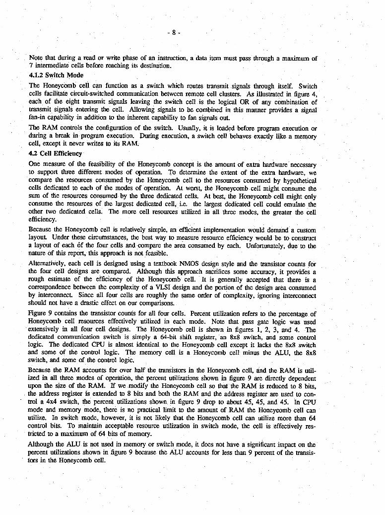
4.0 Honeycomb ArchitectureThe proposed Honeycomb system consists of a control unit and an array of Honeycomb cells. Each Honeycomb cell functions as a CPU, a memory extension, or a communication switch. Collections of cells can serve as multi-cell processing clusters. In a cluster, a single cell serves as the CPU; the other cells merely extend the memory available to the CPU. Processing clusters range in size from a single cell to 64 cells. The control unit manages the flow of data in and out of the cell array and controls the operation of all the processing clusters.An ideal Honeycomb cell is a simple yet multi-purpose building block. Unfortunately, extra hardware is necessary to support three different modes of operation. To maintain a balance between flexibility and simplicity, a lot of the hardware in the proposed cell is used in all three operational modes. To simplify the cell even further, the proposed architecture places some constraints on the way cells are clustered.The configuration of the cell array is determined at compile time. During a pre-processing phase, die cell array is adjusted to match the necessary topology. All cells are loaded with a function (CPU, memory, or switch); switch cells are properly configured; and data is loaded into CPU and memory cells.Connections between adjacent processing clusters need not pass through a communication switch. Connections established through a series of switches are static, circuit-switched connections.4.1 Honeycomb CellThe logical structure of the Honeycomb cell is shown in figures 1, 2, 3, and 4. Figure 5 contains a list of each signal name and its description. The cell consists of a simple ALU, a 64-bit RAM, a 6-bit address register, a 2-bit function register, a 1-bit enable register, a 1-bit I/O register, an 8x8 switch, and control logic. The control signals and clock signals are generated by the controller.The cell functions as a CPU, a memory extension for a CPU, or a communication switch. As shown in figure 6, the contents of the function register determine the mode of the cell. A processing cluster consists of a single CPU cell and up to 63 attached memory cells.Cell clusters are defined in terms of a cartesian coordinate system. Each cell within the cluster is assigned a twos-complement (x,y) address. Both the x-coordinate and the y-coordinate range from -4 to +3. The CPU cell must be located at cell address (0,0). There is also a restriction on the placement of memory cells. From each memory cell there must be a direct horizontal path, through other memory cells if necessary, to the line x=0, and then a direct vertical path, again through other memory cells if necessary, to the CPU.Each cell is directly connected to each of its 8 neighbors. A transmit line from each of the 8 neighbors as well as a data line from the north, south, east, and west neighbors enter the cell as inputs. A corresponding set of output lines leave the cell. A single internal data signal is connected to the north, south, east, ami west neighbors and 8 independent internally generated transmit signals are connected to the 8 neighbor cells. The data lines handle intra-cluster data transfers between memory and CPU cells. The transmit lines handle inter-cluster communication.The configuration of the I/O register allows overlapped VO and data processing. While the processing clusters are working, columns of input data are shifted left across the array through the VO registers until a complete plane of data is in place. The entire input plane is operated on in a single instruction cycle. In a similar vein, a plane of data is output by loading the VO registers and then shifting them out column by column through the right side of the array. To maximize VO bandwidth, input and output are overlapped. Only CPU cells have functional VO registers. All other I/O registers are bypassed as data is shifted through the array.CPU cells signal the controller by setting R0. The controller receives the logical OR of the assertions of the individual CPU cells. Memory cells and switch cells cannot signal the controller.Each cell contains mi enable register to support conditional operations. If its enable register is set, a CPU or memory cell can write data in its RAM. Each instruction can optionally override the enable
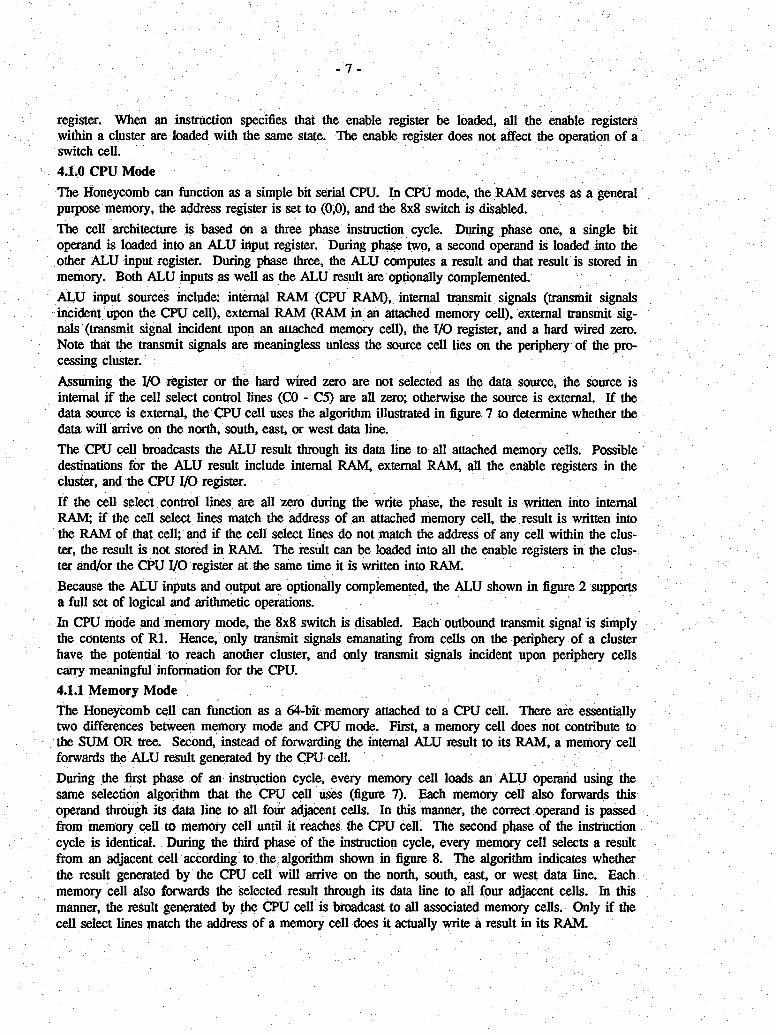
register. When an instruction specifies that the enable register be loaded, all the eatable registers within a cluster are loaded with the same state. The enable register does not affect the operation of a switch cell.4.1.0 CPU ModeThe Honeycomb can function as a simple bit serial CPU. In CPU mode, die RAM serves as a general purpose memory, the address register is set to (0,0), and the 8x8 switch is disabled.The cell architecture is based on a three phase instruction cycle. During phase one, a single bit operand is loaded into an ALU input register. During phase two, a second operand is loaded into the other ALU input register. During phase three, the ALU computes a result and that result is stored in memory. Both ALU inputs as well as the ALU result are optionally complemented.ALU input sources include: internal RAM (CPU RAM), internal transmit signals (transmit signals incident upon the CPU cell), external RAM (RAM in an attached memory cell), external transmit signals (transmit signal incident upon an attached memory cell), the I/O register, and a hard wired zero. Note that the transmit signals are meaningless unless the source cell lies on the periphery of the processing cluster.Assuming the I/O register or the hard wired zero are not selected as the data source, the source is internal if the cell select control lines (CO - C5) are all zero; otherwise the source is external. If the data source is external, the CPU cell uses the algorithm illustrated in figure 7 to determine whether the data will arrive on the north, south, east, or west data line.The CPU cell broadcasts the ALU result through its data line to all attached memory cells. Possible destinations for the ALU result include internal RAM, external RAM, all the enable registers in the cluster, and the CPU I/O register.If the cell select control lines are all zero during the write phase, the result is written into internal RAM; if the cell select lines match the address of an attached memory cell, the result is written into the RAM of that cell; and if the cell select lines do not match the address of any cell within the cluster, the result is not stored in RAM. The result can be loaded into all the enable registers in die cluster and/or the CPU I/O register at the same time it is written into RAM.Because the ALU inputs and output are optionally complemented, the ALU shown in figure 2 supports a full set of logical and arithmetic operations.In CPU mode and memory mode, the 8x8 switch is disabled. Each outbound transmit signal is simply the contents of Rl. Hence, only transmit signals emanating from cells on the periphery of a cluster have the potential to reach another cluster, and only transmit signals incident upon periphery cells cany meaningful information for the CPU.4.1.1 Memory ModeThe Honeycomb cell can function as a 64-bit memory attached to a CPU cell. There are essentially two differences between memory mode and CPU mode. First, a memory cell does not contribute to the SUM OR tree. Second, instead of forwarding the internal ALU result to its RAM, a memory cell forwards the ALU result generated by the CPU cell.During the first phase of an instruction cycle, every memory cell loads an ALU operand using the same selection algorithm that the CPU cell uses (figure 7). Each memory cell also forwards this operand through its data line to all four adjacent cells. In this manner, the correct operand is passed from memory cell to memory cell until it reaches the CPU cell. The second phase of the instruction cycle is identical. During die third phase of the instruction cycle, every memory cell selects a result from an adjacent cell according to the algorithm shown in figure 8. The algorithm indicates whether the result generated by the CPU cell will arrive on the north, south, east, or west data line. Each memory cell also forwards the selected result through its data line to all four adjacent cells. In this manner, the result generated by the CPU cell is broadcast to all associated memory cells. Only if the cell select lines match the address of a memory cell does it actually write a result in its RAM.
- 8 -
Note that during a read or write phase of an instruction, a data item must pass through a maximum of 7 intermediate cells before reaching its destination.4.1.2 Switch ModeThe Honeycomb cell can function as a switch which routes transmit signals through itself. Switch cells facilitate circuit-switched communication between remote cell clusters. As illustrated in figure 4, each of the eight transmit signals leaving the switch cell is the logical OR of any combination of transmit signals entering the cell. Allowing signals to be combined in this manner provides a signal fan-in capability in addition to the inherent capability to fan signals out.The RAM controls the configuration of the switch. Usually, it is loaded before program execution or during a break in program execution. During execution, a switch cell behaves exactly like a memory cell, except it never writes to its RAM.4.2 Cell EfficiencyOne measure of the feasibility of the Honeycomb concept is the amount of extra hardware necessary to support three different modes of operation. To determine the extent of the extra hardware, we compare the resources consumed by the Honeycomb cell to the resources consumed by hypothetical cells dedicated to each of the modes of operation. At worst, the Honeycomb cell might consume the sum of the resources consumed by the three dedicated cells. At best, the Honeycomb cell might only consume the resources of the largest dedicated cell, i.e. the largest dedicated cell could emulate the other two dedicated cells. The more cell resources utilized in all three modes, the greater the cell efficiency.Because the Honeycomb cell is relatively simple, an efficient implementation would demand a custom layout Under these circumstances, the best way to measure resource efficiency would be to construct a layout of each of the four cells and compare the area consumed by each. Unfortunately, due to the nature of this report, this approach is not feasible.Alternatively, each cell is designed using a textbook NMOS design style and the transistor counts for the four cell designs are compared. Although this approach sacrifices some accuracy, it provides a rough estimate of the efficiency of the Honeycomb cell. It is generally accepted that there is a correspondence between the complexity of a VLSI design and the portion of the design area consumed by interconnect Since all four cells are roughly the same order of complexity, ignoring interconnect should not have a drastic effect on our comparisons.Figure 9 contains the transistor counts for all four cells. Percent utilization refers to the percentage of Honeycomb cell resources effectively utilized in each mode. Note that pass gate logic was used extensively in all four cell designs. The Honeycomb cell is shown in figures 1, 2, 3, and 4. The dedicated communication switch is simply a 64-bit shift register, an 8x8 switch, and some control logic. The dedicated CPU is almost identical to the Honeycomb cell except it lacks the 8x8 switch and some of tiie control logic. The memory cell is a Honeycomb cell minus the ALU, the 8x8 switch, and some of the control logic.Because the RAM accounts for over half the transistors in the Honeycomb cell, and the RAM is utilized in all three modes of operation, the percent utilizations shown in figure 9 are directly dependent upon the size of the RAM. If we modify the Honeycomb cell so that the RAM is reduced to 8 bits, the address register is extended to 8 bits and both the RAM and the address register are used to control a 4x4 switch, the percent utilizations shown in figure 9 drop to about 45, 45, and 45. In CPU mode and memory mode, there is no practical limit to the amount of RAM the Honeycomb cell can utilize. In switch mode, however, it is not likely that the Honeycomb cell can utilize more than 64 control bits. To maintain acceptable resource utilization in switch mode, the cell is effectively restricted to a maximum of 64 bits of memory.Although the ALU is not used in memory or switch mode, it does not have a significant impact on the percent utilizations shown in figure 9 because the ALU accounts for less than 9 percent of the transistors in the Honeycomb cell.
- 9 -
The 8x8 switch accounts for about 15 percent of the transistors in the Honeycomb cell. Since it is not used in CPU or memory mode, the switch has a moderate impact on resource utilization in CPU and memory mode.Note that almost every bit within the Honeycomb cell RAM drives an internal bus as well as an external gate. Most bits drive the select lines of the 8x8 switch. A standard RAM probably could not drive the additional load. Without thorough simulation, however, it is not clear what type of design modifications would suffice. Again, due to the nature of this report, figure 9 ignores the possibility that a costlier design (in terms of transistors) would be necessary.While the cell comparisons shown in figure 9 are indicative of the efficiency of a single Honeycomb cell, they do not reflect the efficiency of a large processing cluster. To measure the efficiency of a large processing cluster, we compare the resources consumed by a 64-cell cluster to the resources consumed by a comparable dedicated processing element. This processing element is similar to the dedicated CPU cell mentioned above except it contains 4K-bits of memory and it does not need interface circuitry to allow it to coalesce with other processing elements. Figure 10 contains transistor counts for the two implementations. Processing clusters smaller than 64 cells have percent utilizations between that of the 64-cell cluster and that of a single Honeycomb cell.4.3 Embedding Interconnection PatternsMost planar interconnection patterns are easily embedded in the proposed Honeycomb architecture. As long as a pattern has a planar topology, the Honeycomb can be configured to match its structure. Figures 11, 12, and 13 show several common interconnection patterns embedded in the Honeycomb. The mesh pattern is used in image processing algorithms and matrix operations; the binary tree pattern is used in searching and sorting algorithms; and the FFT pattern is used to compute an FFT.The proposed architecture is also amenable to less structured planar interconnection patterns. As indicated earlier, however, additional research is necessary to identify algorithms which fall into this category.4.4 ExtensionsThere are several potential extensions to the Honeycomb cell design shown in figures 1, 2, 3, and 4.1. In the proposed implementation of the Honeycomb cell, 8 bits of RAM as well as the entire 6-
bit address register are unused in switch mode. Only 56 bits are necessary to control the switch. If the RAM contained only 50 bits, and both the RAM and the address register were used to control the switch, resource utilization would increase somewhat in switch mode. Resource utilization would also decrease in CPU and memory mode, but only slightly.
2. In an ideal Honeycomb architecture, collections of cells can serve as multi-bit CPUs. The proposed architecture does not support multi-bit CPUs. With a few modifications, however, the proposed architecture could support a restricted multi-cell CPU configuration. If the carry out of each ALU is connected to the carry in of its north neighbor, we could create vertically oriented multi-cell CPUs. In extended CPU mode, a cell would derive its carry from an adjacent cell; in normal CPU mode, a cell would derive its carry internally. The suggested north-south orientation of the multi-cell CPU is convenient because it guarantees an organized I/O scheme given the east-west orientation of the I/O network.The suggested multi-cell CPUs suffer two primary drawbacks. First, the cascaded ALUs will behave like extremely slow ripple carry adders and second, multi-cell CPUs will be restricted to 512 words of memory. Each bit of the CPU will only have a single column of attached memory cells and the maximum length of that column is 8. The limit on the length of that column could be relaxed, but propagation delays would correspondingly increase.
3. In the proposed implementation of the Honeycomb architecture, switch cells are merely static switches. Since every cell has an ALU and RAM, a slightly modified Honeycomb cell might be able to support some form of dynamic packet-switched data routing mechanism.
- 10-
5.0 ConclusionThe Honeycomb architecture is a novel fine grain parallel architecture which features an array of identical processing/memory/communication cells. It derives most of its potential from a uniform and unbiased structure. A Honeycomb can be configured to match nearly any planar topology. Cells are multi-purpose building blocks allocated to memory, processor, and communication functions as dictated by each algorithm.The Honeycomb cell presented in this report demonstrates the feasibility of the Honeycomb concept. It permits three distinct modes of operation with a minimum of support hardware. Demonstration of a functional Honeycomb cell paves the way for further research concerned with mapping algorithms onto the Honeycomb architecture.

-11 -
Appendix A AAP2 [23]
IntroductionAAP2 is a cellular array intended primarily for image processing and CAD applications. It features pseudo-MIMD operation and a flexible interconnection network. AAP2 consists of a control unit (data buffer memory, instruction memory, and a scalar processor) and a 256 x 256 array of 1-bit processing elements.
Interconnection NetworkWithin the array, each processing element is connected to its eight nearest neighbors. Two input lines from each of the four nearest neighbors and one input line from the other four neighbors enter the PE. An equal number of output lines leave the PE. The output signals are a programmable combination of input signals and internal signals. AAP2 supports a single cycle, long distance data transfer through these communication lines.
Processing Element ArchitectureEach 1-bit processing element contains an ALU, a versatile data transfer unit, a 9 x 16 bit register file, a 16-bit control register, and local memory. The register file, local memory, or the input signals from neighboring PEs serve as ALU inputs.AAP2 is based on a two-address instruction format. Three types of instructions are supported: data transfer between the controller and the processor array, memory to register operations, and input signal to register operations.AAP2 implements pseudo-MIMD control by modifying each instruction with the control register. Both ALU functions and data routing directions can be altered.
Processing Element Local MemoryEach processing element contains an 8K bit local memory.
ControllerThe controller directs the overall operation of the processor array. It broadcasts 40-bit instructions to all the PEs.
ConclusionThe most noteworthy feature of the AAP2 architecture is the flexible interconnection network. It permits a single cycle long distance data transfer. A similar mechanism may find a home in the Honeycomb architecture.
- 12 -
IntroductionThe Content Addressable Array Parallel Processor (CAAPP) is a cellular array intended primarily for image processing applications. CAAPP consists of a controller and a 512 x 512 array of 1-bit processing elements. Each PE contains a processor, local memory, and a small register file.
Interconnection NetworkEach PE within the processor array is directly connected to each of its four nearest neighbors.
Processing Element ArchitectureEach PE contains contains six general purpose 1-bit registers, a 1-bit memory buffer, a 128-bit local memory, and a 5-function ALU.Each instruction executes in a single two-phase cycle. During phase one, two source operands from the register file and/or memory buffer are applied as inputs to the ALU. The ALU also begins to perform the desired function. Each of the two ALU inputs is optionally complemented. Note that one of the ALU inputs is also the source for data transferred to neighbor PEs. During phase two, the result of the ALU operation or data transferred from a neighbor PE is written into either a register or the memory buffer. The ALU output is optionally complemented.The ALU supports five functions: XNOR, NOR, complemented add, or passing either of the two ALU inputs.CAAPP employs a read-modify-write operation to handle interactions with local memory. Each instruction contains a memory address field. During the first phase of instruction execution, the contents of that memory location are copied into the memory buffer. The PE may Or may not select the memory buffer as an ALU input. Late during the second phase of instruction execution, the contents of the memory buffer are copied back into the same memory location. If the instruction modified the memory buffer, the memory location is correctly updated; if not, the memory location is unchanged.PE masking is accomplished through a selective writeback facility. All PEs execute all instructions, but only those with an active activity register write results into the memory buffer or the register file. Note that each instruction may optionally override the masking facility.The X register of each PE is directly connected to a response counter. The response counter allows the controller to determine the exact number of PEs responding to a particular query.
Processing Element Local MemoryAs indicated in the previous section, each PE contains a 128-bit local memory.
ControllerThe controller broadcasts instructions to all PEs. The processor array provides feedback to the controller in three forms. The controller can detect whether any of the PEs have a particular status, count the PEs with a particular status, or select the first PE with a particular status.
ConclusionThe most noteworthy features of the CAAPP architecture are the read modify write operation and the selective writeback facility. They provide a simple mechanism to control PE masking. Note that these features could easily be incorporated into the Honeycomb architecture.
CAAPP [35]

- 13 -
IntroductionCAP (Cellular Array Processor) is an extended cellular array architecture intended primarily for image processing applications. CAP features overlapping of execution and I/O, pseudo-MIMD control, and a reconfigurable network.CAP contains a'master controller, an I/O controller, a large array of 1-bit processing elements, and a large two-dimensional access memory.
Interconnection NetworkThe processor array consists of a square array of processing elements embedded in a square array of switching elements. Each switching element is connected to four PEs, several I/O lines, and several broadcast lines. Each switching element handles data transfers between PEs, communication between a PE and the switching element itself, and data transfers to and from an VO buffer. Each switching element has two special shift registers that allow it to overlap interprocessor data transfers with VO transfers.It is not necessary that data in all switching elements move simultaneously in the same direction. The direction of data transfer is optionally specified by a flag in each switching element
Processing Element ArchitectureWithin the processor array, each 1-bit PE consists of a full adder, a register file, a partial-sum register, a control register, several status flags, and local memory.CAP implements MIMD-like control with both an instruction modification function and an address modification function. All PEs receive the same instruction word from the controller, but each PE modifies the instruction word with its own control register. The address modification function allows each PE to access a different bit in the partial-sum register.
Processing Element Local MemoryCAP is an SIMD architecture, i.e. all PEs execute instructions broadcast by a central controller. Hence, each PE must contain enough local memory to accommodate only a portion of the data associated with an image processing application.
ControllerThe master controller is responsible for overall control of CAP. It translates commands issued by a host computer into a sequence of microinstructions which it broadcasts to the processor array and the I/O controller. The I/O controller handles data transfers to and from the two-dimensional memory.
ConclusionThe most notable feature of the CAP architecture is the flexible data routing mechanism. Different PEs can transfer data in different directions in the same instruction cycle. The Honeycomb architecture may incorporate a similar mechanism.
CAP [21]
- 14 -
IntroductionThe Configurable, Highly Parallel (CHiP) computer is an MIMD multiprocessor architecture which integrates a programmable interconnection network with a fairly large set of processing elements. It offers the uniformity and locality characteristic of systolic arrays, but maintains the flexibility of a general purpose processor.The CHiP computer consists of a large set of identical processing elements, a switch lattice, and a controller.
Interconnection NetworkThe switch lattice is the heart of the CHiP computer. It is a regular structure composed of programmable switches connected by data busses. The PEs are not connected to each other; instead they are inserted at regular intervals within the switch lattice.The most important characteristics of the switch lattice are the corridor width (number of switches that separate two adjacent PEs) and the switch degree (number of incident data paths). Both influence PE utilization and the ease of embedding a particular interconnection pattern in a lattice. A corridor width of four and a switch degree of eight guarantee reasonable results for most applications. Note that a complete binary tree can be embedded in a square switch lattice with corridor width equal to one and switch degree equal to four with only a single unused PE.Each switch in the lattice can store several configuration settings. A particular setting establishes a direct, static connection between two or more of the incident data busses.
Processing Element ArchitectureCHiP is an MIMD architecture, i.e. PEs execute instructions stored in their local memories. Hence, each PE must be a full fledged processor. Each must also have an efficient interface to the switch lattice so that it can selectively exchange information with the PEs to which it is connected.
Processing Element Local MemorySince CHiP is an MIMD architecture, each local memory must be large enough to accommodate both code and data.
ControllerThe CHiP controller directs the operation of the CHiP processor array. It has two primary functions.1. The controller is responsible for loading both the appropriate configuration settings into switch
memory and programs into PE local memory. The switch memories are loaded through a separate interconnection "skeleton" prior to actual processing (in parallel with PE program memory loading).
2. Immediately prior to processing, the controller broadcasts a command to all switches to invoke a particular configuration setting. When the controller initiates processing, all PEs synchronously execute instructions stored in their local memories. If a new phase of processing is required, the controller broadcasts, a command to all switches to invoke another configuration setting, effect tively restructuring the entire lattice with a single instruction.
ConclusionThe most noteworthy feature of the CHiP architecture is the switch lattice. It is responsible for a dramatic increase in the flexibility of interprocessor connections. ,
CHiP [30]

-15 -
IntroductionThe Connection Machine is a massively parallel processor which integrates a cellular array into a packet-switched communication network. It consists of an array of processing elements, an array of routing units, and a controller. The routing units provide efficient and transparent communication between arbitrary pairs of processing elements.
Interconnection NetworkEach processing element is directly connected to its four nearest neighbors. The PEs are also interconnected through a packet-switched network modeled on a Boolean n-cube topology. The network uses an adaptive routing algorithm.There is a single routing unit for every 16 PEs. A router with address i is connected to a router with address j if i and j differ in a single bit position. Each router is responsible for injecting new messages from the PEs it serves into the network, forwarding messages between routing units, receiving and delivering messages to the PEs it serves, and buffering messages if the network becomes congested.A PE initiates a message by sending a message packet to its Router-Data flag. The packet consists of an address followed by data. The router accepts or rejects the message based on its current loading. Notification of acceptance or rejection is relayed to the PE through its Router-Acknowledge flag. If the message is rejected, the PE simply retransmits at a later time.
Processing Element ArchitectureEach processing element within the Connection Machine contains a serial arithmetic-logic unit, 4K bits of local memory, 8 general purpose flags, and 8 special purpose flags.The instruction cycle consists of three phases. During the first phase, an operand bit is read from local memory. During the second phase, a second operand bit is read from local memory, a third operand is read from one of the flags, and the three operands are combined according to a specified logic operation. The operation produces two result bits. During the third cycle, the flag result is written to an internal flag and the memory result is written to local memory.During each instruction cycle, the NEWS flag is updated with the flag result from either the north, south, east or west neighbor.All PEs receive the same instruction from the control unit, but, depending on the state of one of its flags, a PE may or may not execute the instruction.Each group of 16 PEs is connected in a daisy-chain. The Daisy-Chain flag reads the flag output of the PE ahead of it on the daisy-chain. This allows the 16 PEs to function as a single 16-bit PE.
Processing Element Local MemoryAs mentioned in the previous section, each processing element includes 4K bits of local memory.
ControllerThe microcontroller, under the direction of a conventional host, broadcasts nanoinstructions to the processing elements. The host specifies high-level macroinstructions and the microcontroller translates them into a sequence of nanoinstructions.There are two mechanisms for passing information from a PE to the microcontroller. First, local memory can be read over the nanoinstruction bus. Second, a PE can assert a global or error signal.
Conclusion
Connection Machine [19]

- 16 -
The most notable feature of the Connection Machine is its packet-switched communication network. The network allows efficient and transparent communication between arbitrary pairs of processing elements. Since the communication network is physically abstracted from the processor array, it may be possible to incorporate a similar network into the Honeycomb architecture.
- 17 -
IntroductionDADO is a fine-grain parallel, tree-structured architecture designed to efficiently execute production systems (rale-based expert systems). A full-scale version of DADO consists of a large set of PE s interconnected to form a complete binary tree. Each PE contains a processor, a small amount of local memory, and a specialized I/O switch. “
DADO [31]
Interconnection NetworkThe I/O switch connects a PE to its parent and its left and right children. Each PE can execute in SIMD or MIMD mode. In SIMD mode, the PE executes instructions broadcast by some ancestor PE within the tree. The I/O switch accepts instructions from the parent PE and also passes the instructions to the left and right child PEs. In MIMD mode, the PE executes instruction stored in its local memory. Die I/O switch broadcasts the instructions read from local memory to its children and ignores any instructions broadcast by its parent.When a PE enters MIMD mode, it and its descendents are effectively disconnected from its ancestors. The PE broadcasts instructions to be executed by its descendents, assuming they are in SIMD mode. Thus, the DADO machine can be logically divided into several partitions, each executing a distinct task (multiple SIMD execution). Die partitioning capability allows DADO to concurrently execute a large number of primitive pattern matching operations.
Processing Element ArchitectureDue to the nature of the DADO application environment (production systems), each PE must contain a full fledged processor. Although details of the production version are scarce, the DADO prototypes are designed with 8-bit general purpose microprocessors.
Processing Element Local MemorySince each PE is capable of executing in either SIMD or MIMD mode, the memory within each PE must be large enough to accommodate a portion of a production system interpreter (code) as well as productions and working memory elements (data). Die prototype PEs contain 16K bytes of local memory.
ControllerA single conventional microprocessor, adjacent to the root of the DADO tree, controls the operation of the entire ensemble of PEs. Among other things, the controller determines the configuration of the DADO tree, i.e. which PEs execute in SIMD mode and which PEs execute in MIMD mode.
ConclusionThe most noteworthy feature Of the DADO architecture is the reconfigurable multiple-SIMD tree structure. Unfortunately, a tree structure does not provide the level of connectivity required by the Honeycomb architecture.

- 18 -
IntroductionThe ICL DAP (Distributed Array Processor) is a 4096 element processor array. It consists Of a control unit, an interconnection network, and a 64 x 64 array of 1-bit processing elements.
Interconnection NetworkThe DAP has both a local interconnection network and a global interconnection network. Each processing element is directly connected to its four nearest neighbors. Edge processors are connected to each other in a cyclic fashion. Note that the edge connections may be disabled under program control. Each PE is also connected to a row highway and a column highway. DAP contains 64 row highways and 64 column highways which can send or receive data from a set of 64-bit registers within the control unit
Processing Element ArchitectureEach PE within the processor array contains a fairly simple 1-bit processor, 4K bits of local memory, and a programmable activity register. Certain instructions are ignored if the activity register is reset.
Processing Element Local MemoryAs mentioned in the previous section, each PE contains 4K bits of local memory. Note, however, that the local memories can be configured as one large 2M byte memory for I/O operations.
ControllerThe control unit broadcasts instructions to the processor array. One important instruction causes each PE to AND the contents of its activity register onto either a row or column highway. A designated register within the control unit is then loaded with the status of the set of 64 highways.
ConclusionThe most notable feature of the DAP architecture is the ability to configure the local memories as a large one-dimensional memory. Unfortunately, the scheme is infeasible in a cellular array containing a significantly larger number of processing elements.
DAP [27]
- 19 -
IntroductionThe Hughes 3-D Cellular Array is a massively parallel SIMD architecture intended for two- dimensional image and signal processing. The system consists of a controller and a N x N array of identical 1-bit processing elements contained on a stack of silicon wafers. The processing elements are arranged horizontally, with the components of each PE assembled vertically. Each wafer in the stack contains an N x N array of one particular resource (memory, accumulator, replicator, counter, or comparator). The wafers are connected by address, data, and control busses that pass vertically through the stack.
Interconnection NetworkMost interprocessor communication is handled by the memory wafer. Each cell in the memory wafer is directly connected to its four nearest neighbors. The replicator wafer, however, allows data to be broadcast across the entire array or N data values to be broadcast down the N columns of the array.
Processing Element ArchitectureEach 1-bit processing element is composed of several components: accumulator, memory, replicator, counter, and comparator. The components are connected via a 1-bit data bus.Most of the processing in the 3-D computer occurs in the memory and accumulator wafers. Each cell in these two wafers contains a 16-bit shift register and circuitry for assorted logical functions.The memory shift register is used to store data and to transfer data to and from adjacent PEs. The memory cell can store the logical OR of any subset of its data sources (N, S, E, W, data bus, shift register). It can also invert data output to the data bus to facilitate twos-complement subtraction.The accumulator cell is similar to the memory cell except a full adder is included and there is no nearest neighbor connection.Each cell in the counter wafer contains a 5-bit counter which can count the number of times a particular event occurs.Each cell in the comparator wafer contains a 16-bit shift register. A comparison value may be loaded into this register and compared to the contents of the memory or accumulator shift register. The comparator cell has three outputs: greater than, less than, and equal.The replicator plane can be used to perform certain binary operations such as determining whether a given region of the array contains any data.
Processing Element Local MemoryEach processing element contains several 16-bit shift registers. This is the full extent of local memory.
ControllerThe control unit is responsible for program storage and sequencing, as well as control of the processor array. The controller communicates with the array through address and control busses that pass through all the wafers.
ConclusionThe most noteworthy feature of the Hughes 3-D computer is its three-dimensional structure. Depending on the-application, different sets of wafers can be combined to form a functional system. Such a strategy increases flexibility and parallelism. In artificial intelligence applications, it may be beneficial to design a new wafer which houses a partial or complete interconnection network.
Hughes 3-D Cellular Array [13]

-20 -
IntroductionThe Linkoping Image Parallel Processor (LIPP) is a cellular array intended mainly for image processing. LIPP consists of a controller and a 16 x 16 array of 1-bit processing elements.
Interconnection NetworkEach PE is connected to its eight nearest neighbors. A PE can read data from a neighbor memory just as it can read data from its own local memory. A PE cannot, however, write data in a non-local memory.
Processing Element ArchitectureEach 1-bit processing element contains an ALU, two variable length shift registers, a shiftable index register, a shiftable up/down counter, a 1-bit counter enable register, a carry register, a 1-bit PE enable register to allow data dependent masking, a 1-bit status register to signal a condition to the controller, and a 64K-bit local memory.ALU inputs include the shift register outputs, the counter output, the counter enable register, local memory, and each of eight neighbor memories. Destinations for ALU results include the carry register, the shift register inputs, the counter input, the index register input, the status register, the counter enable register, the PE enable register, and local memory. Note that while a PE may read data from a neighbor memory, it may not write to that memory.
Processing Element Local Memory Each PE possesses a 64K-bit local memory.
ControllerThe controller directs the overall execution of the processor array. It is responsible for loading image data into the array and broadcasting instructions to the array
ConclusionThe most interesting feature of the LIPP processor is the ability to read from but not write to the eight memories adjacent to a particular PE. A similar policy may be incorporated in the Honeycomb processor.
LIPP [7]
- 21 -
IntroductionThe MlTKE processor is a massively parallel processor intended primarily for artificial intelligence applications. The processor features efficient communication between arbitrarily chosen processor pairs, hardware message routing support, and self-adjustment to processor absence or failure.The MITRE processor imposes a hierarchical grouping of processing elements. An array of 16 x 16 processing elements is constructed on a wafer and is interconnected with a system of relatively short communication busses. A 16 x 16 array of wafers is arranged on a rack and is interconnected with
. the same bus structure found on a wafer. Finally, 16 racks are stacked to form a network of one million processors. The racks are connected through a set of relatively short communication busses oriented orthogonal to each rack.
Interconnection NetworkInterprocessor communication relies on a regular bus structure and a message passing mechanism. Each processing element is connected to four busses: two oriented horizontally and two oriented vertically. Each bus is connected to either 8 or 16 PEs. All PEs are responsible for bus arbitration (to avoid loss of the bus due to loss of the arbiter); all processor to processor communication is buffered; and routing of messages is a local function performed by each PE.Message passing proceeds as follows. The PE message passing logic receives messages from within the PE and from each of its four ports. It selects a message and an initial port according to a well defined algorithm. The selected destination address is decoded to yield a 16-bit word. Each bit in the word corresponds to a PE connected to the port and is set if the PE lies in the direction of the final destination. Then the PE bus arbiter requests control of the bus. If the cell gains control of the bus, its reads a 16-bit word that has the same bit-to-cell correspondence as the decoded destination address; the set bits identify each cell that is free to accept a message. The arbiter compares the two 16-bit words and chooses one bit that matches. Then it forwards the message to the matching PE. If there is no match or control of. the bus is not granted, the destination address decoder tries the next port, If unsuccessful at each of the other three ports, the destination address decoder mOves on to die next message.
Processing Element ArchitectureEach PE within the MITRE processor is a full fledged processor. It contains a CPU, local memory, message passing logic, and four I/O ports. The prototype system uses MC68000 microprocessors to emulate the PEs.
Processing Element Local MemoryEach PE contains several K-bytes of local memory.
ControllerThe central controller has overall responsibility for the processor array.
ConclusionThe most noteworthy feature of the MITRE processor is the bus-structured message passing mechanism. Since dynamic message passing is quite important in many AI applications, a variation of the bus-structured message passing mechanism may find a home in the Honeycomb architecture.
MITRE Processor [16]

-22 -
IntroductionThe Massively Parallel Processor (MPP) is an SIMD processor array intended primarily for image processing applications. The system consists of a 128 x 128 array of 1-bit processing elements, an array control unit, and a staging memory which buffers and reformats data transferred to and from the processor array.
Interconnection NetworkEach processing element within the array is directly connected to its four nearest neighbors. The connections between edges of the array are under program control. The top and bottom edges can either be connected or left open. The left and right edges allow four topologies: open, cylindrical, open spiral, and closed spiral. All PEs simultaneously transfer data in die same direction.
Processing Element ArchitectureEach 1-bit processing element within the processor array contains 6 1-bit registers (A, B, C, G, P, S), a shift register with a programmable length, local memory, a full adder, and other logic.Logic operations combine the state of the P register with the state of the date bus to yield a new state for the P register.All routing operations transfer the contents of the P register to a neighboring P register. Recall that all PEs transfer data simultaneously in the same direction.The only arithmetic operation explicitly supported is addition. The adder adds the contents of the carry bit in C, the A register, and the P register. It stores the sum bit in the B register and updates the carry register. Successive sum bits are stored in local memory and/or in the shift register for later operations.The G register holds a mask bit which controls PE activity. Note that each instruction may override this masking facility.The S registers within each row of the processor array are connected together to allow input and/or output data to shift across the array. An entire plane of date can be shifted across the array while date processing is in progress. One cycle is required to transfer a plane of data between the S registers and local memory.
Processing Element Local MemoryThe initial configuration of the MPP includes lK-bits of local memory per PE. Storage is expandable to 64K-bits per PE.
MPP [2]
ControllerThe array control unit consists of three independently operating control units: the PE control unit, the I/O control unit, and the main control unitThe PE control unit broadcasts instructions to the processor array. Each instruction contains one or more operations as well as a memory address. Note that it is possible to combine an arithmetic operation and a logic or routing operation in a single instruction.The I/O control unit controls the S registers and the staging memories.The main control unit sends commands to the PE control unit and the I/O control unit These commands are subsequently translated into sequences of appropriate microinstructions.
Conclusion

-23 -
The most noteworthy characteristics of the MPP are its simplicity and regularity. Unfortunately, by definition, the Honeycomb architecture is significantly more complicated.
-24 -
NETL [8, 9]
IntroductionNETL is a marker-passing massively parallel architecture for representing knowledge in the form of semantic networks. In theory, NETL is composed of an extremely large set of simple processing elements (nodes) and a correspondingly large set of dedicated bidirectional connections (links) between those processing elements. An "element" in NETL is composed of a single node and a four-wire link. Nodes communicate by passing single-bit markers across links. The links are dedicated private lines, enabling a lot of marker traffic to proceed in parallel. A NETL system is wired up to form the nodes and links of a semantic network.If NETL is completely hard wired, it is extremely costly (if not impossible) to add new private links as new information is added to the network. In addition, with a hard wired implementation, it is impossible to use the same network with different knowledge bases.This summary describes a 960 element processor array and a flexible switching network which are timeshared to implement a NETL system of 960 or more elements.
Interconnection NetworkThe switching network that establishes links between nodes is called a hashnet. It a 960 x 960 seldom-blocking switching network. The heart of the hashnet is a 15-way selector cell. It connects its input to any of its 15 outputs according to the contents of a four-bit state register. A value of zero indicates the cell is unused, i.e. its input is not connected to any output. Fifteen of these cells are combined (the outputs of all cells are wired together) to form a 15 x 15 switching element. The switching elements are arranged in four consecutive 128 x 1 rows. The outputs (1920) of each row are wired to the inputs (1920) of the next row with a fixed but randomly chosen pattern of wires.Each of the 960 processing elements is randomly connected to two inputs in the first row of switching elements and two outputs in the last row of switching elements. (Note that these connections correspond to a single link. The network is timeshared to create the effect of multiple links.) To establish a connection from a given input to a given output, a marking signal is broadcast from the input to all selector cells and outputs that can be reached. Only non-busy cells participate in this process. If the signal reaches the desired output, one of the marked paths is traced back to the source, with the selector cells along the way being set up appropriately. Note that an occasional failure to find a connection is not disastrous. Since each node in NEIL contains four links, the hashnet is timeshared 4 ways for every set of 960 elements. If we fail to find a connection, we simply try a different link; i.e. a different time slice.
Processing Element ArchitectureThe NETL processing element contains a unique serial number, 16 write-once flag-bits which indicate the type of the element, and 16 read/write marker bits which indicate the current state of the elementThe processing elements execute commands broadcast by the controller. Commands typically specify that all elements with a particular bit-pattem send a 1-bit signal across either incoming or outgoing link-wires, and that any element receiving such a signal should set or clear certain marker bits.It is also possible to direct a command to a single element, or to get an element with a particular bit- pattem to report its serial number over the common bus.
Processing Element Local MemoryThe individual processing elements have no local memory above and beyond the 32 flag and marker bits.
Controller

-25 -
The marker-passing mechanism is under the overall control of an external controller. It broadcasts commands to the NETL elements.
ConclusionThe most noteworthy feature of the NETL system is the hashnet. Because of its random internal structure and redundancy (1920 inputs and 1920 outputs for 960 processors), the hashnet nearly always provides 960 unblocked bidirectional links between arbitrary pairs of processing elements. Since most artificial intelligence applications require communication between arbitrary pairs of processing elements, the Honeycomb architecture may employ a variation of the hashnet.
-26 -
IntroductionNON-VON 4 is a massively parallel MSIMD tree-structured architecture intended for commercial data processing. The system consists of a tree-structured SIMD processor array and a number of large processing elements (LPEs) capable of serving as a control processor for a portion of the tree structure.
Interconnection NetworkWithin die processor array, each PE is connected to its parent PE and its left and right child PEs. In addition, each PE above a certain level in the tree structure is connected to an LPE. The set of LPEs are interconnected through a high bandwidth multistage interconnection network.
Processing Element ArchitectureEach PE within the processor array is a simple custom 8-bit processor. Each LPE, however, is an off-the-shelf microprocessor such as a 68000.
Processing Element Local MemoryEach PE within the processor array contains 64 bytes of local memory. Each LPE, however, contains from 500K to 1M bytes of local memory.
ControllerEach LPE can serve as a controller for a portion of the processor array. It broadcasts instructions to the PEs under its control.
ConclusionThe most noteworthy feature of the NON-VON architecture is the inclusion of several control processors. Each controller can oversee the operation of a portion of the processor array. Unfortunately, a tree structure does not provide the level of connectivity required by the Honeycomb architecture.
NON-VON 4 [29]

-27 -
IntroductionThe PROPAL H Computer is a linear SIMD processor array containing 128 to 2048 1-bit processing elements.
Interconnection NetworkEach PE is connected to the PEs immediately before and after it in the linear array. In a single instruction cycle, a PE can transfer up to 16 bits of information to a neighbor PE.
Processing Element ArchitectureTyh l-bit processing element contains an ALU, local memory, a conditional flag, and a 16-bit "lift register”. ALU operations include all boolean functions, addition, multiplication step, and conditional shiftThe lift register serves two functions. It can function as a pair of memory address registers or it can function as a shift register to facilitate interprocessor communication. In a single instruction, the lift register can transfer up to 16 bits of information to a neighbor PE or the controller. The lift register can be recirculated, loaded with data from another PE, or loaded by the control unit.
Processing Element Local MemoryEach PE employs a two-level hierarchy of local memory. The low level of the hierarchy consists for 256 bits of fast memory. The high level consists of 4K or 16K bits of significantly slower memory.
ControllerThe control unit is responsible for overall control of the processor array. It broadcasts instructions to the processor array.
ConclusionThe most notable feature of the PROPAL II Computer is the lift register. It enables a single instruction to orchestrate the transfer of up to 16 bits of data. If the Honeycomb architecture could benefit from a multi-bit data transfer, a construct similar to the lift register could be incorporated.
PROPALH [33]

-28-
IntroductionThe Pyramid Computer is a massively parallel processor intended for image processing, graphics, and spatial problem solving. The architecture consists of a pyramidal array of 1-bit processing elements executing in SIMD mode. The system effectively combines features of both mesh-connected architectures and tree machines.
Interconnection NetworkEach processing element (except those on the periphery of the pyramidal structure) is directly connected to thirteen other PEs: eight neighbors on the same level, four children in the next lower level, and one parent on the next higher level. If the lowest level of the pyramid contains X PEs, the entire pyramid contains about (4/3)X PEs.
Processing Element ArchitectureEach 1-bit processing element contains an ALU, a 1-bit P register, thirteen inputs, a programmable enable register, and local memory. All interprocessor communication is routed through die P register.Each PE is capable of several types of instructions: pattern matching, loading and storing the P register, and register to memory bit-serial arithmetic. Pattern matching consists of comparing a 14-symbol pattern broadcast by the controller against the contents of all P registers accessible to the PE. Each symbol is 0, 1, or "don’t care".
Processing Element Local MemoryThe Pyramid Computer is an SIMD architecture, i.e. all PEs execute instructions broadcast by the controller. Each PE must contain enough local memory to accommodate the data required by a particular application.
ControllerThe controller broadcasts instructions to the processor array. An instruction word includes a function along with either a local memory address or a pattern.At one edge along the base of the pyramid is a special border register, one bit of which is directly connected to each of the edge PEs. Most data transfers between the controller and the processor array are routed through this border register.The controller can also perform a global OR of the contents of all P registers.
ConclusionThe most noteworthy feature of the Pyramid architecture is the pyramid structure itself. Unfortunately, a pyramid structure does not provide the level of connectivity required by the Honeycomb architecture.
Pyramid Computer [32]
- 29 -
IntroductionThe Reconfigurable Cellular Array Processor (RCAP) is a large-scale processor array intended for image processing applications.The system contains a square array of memory-augmented processing elements interconnected in either a mesh configuration or a tree configuration. The mesh configuration is suited to pixel-level image processing; the tree configuration is suited to region-level image processing. Because the processor array is easily reconfigured, pixel-level and region-level image processing can be completed without loading the processed image to and from the host computer after pixel-level operations have completed.
Interconnection NetworkRCAP is a square array of processing elements. Within each row of the array, each PE is directly connected to its left and right neighbors. The PEs at the ends of the rows are also connected together. Adjacent rows in the array are connected through a bidirectional omega network.
Processing Element ArchitectureThe RCAP architecture does not place many specific requirements on the PE architecture. All PEs must execute all arithmetic and logic functions necessary for typical image processing applications. In addition, each PE must efficiently exchange information with the PEs to which it is connected.
Processing Element Local MemoryRCAP is an SIMD architecture, i.e. the PEs execute instructions broadcast by a processor controller. PE local memory must only accommodate the image data operated on by the PE.
ControllerEach row in the processor array contains three controllers: a data controller, a processor controller, and a network controller.The data controller controls the transfer of data from the host computer to the PEs. The network controller controls the configuration of the bidirectional omega network. The processor controller broadcasts instructions to the PEs. It can also activate or deactivate any processor within the row.Before execution begins, the host loads three sets of data: data for the PEs, programs for the processor controllers, and a set of predefined configurations for the network controllers. When the host executes a command, it specifies an upper and a lower row address. Hence, the host may load a set of successive controllers with the same information (at the same time).
ConclusionThe most noteworthy feature of the RCAP architecture is the reconfigurable interconnection network. While dynamic reconfiguration is important to the Honeycomb architecture, the Honeycomb architecture demands a more robust interconnection network.
RCAP [5]

- 30 -
IntroductionThe Semantic Network Array Processor (SNAP) is a cellular array intended for AI applications that use semantic networks to represent knowledge. The architecture consists of an array of identical microprogrammed processing elements. Each processing element contains a processor, a content addressable memory, and a communication unit, hi typical applications, each PE is dedicated to one node in a semantic network.
Interconnection NetworkEach PE is connected to its four nearest neighbors. All interprocessor communication is based on a message-passing mechanism. To send a message, a PE must specify the actual message as well as the address of the destination PE. The routing mechanism is described in the next section.
Processing Element ArchitectureEach processing element contains a content addressable memory (CAM), a microprogrammed processing unit (PU), and a communication unit (CU). Recall that each PE is dedicated to a node within a semantic network.The CAM consists of cell memory and pointer memory. The cell memory defines the node which is assigned to the PE. The pointer memory stores both relation names and addresses of other nodes (PEs) that relate to this node. The pointer memory stores addresses of nodes (PEs) that point to this node and addresses of nodes that this node points at. The CAM also contains 16 general purpose flags.The PU processes the contents of CAM and controls the communication unit. It contains a small set of general purpose registers, a control store, and an ALU. PU functions have the following general format (<opcode> <argl> <arg2> <arg3>), where <opcode> defines the instruction, <argl> and <arg2> are conditions to be matched, and <arg3> is a flag to be set when those two conditions are matched. <argl> and <arg2> can be nodes, relations, flags, or "don’t care".The CU handles data transfers between PEs. A data transfer instruction consists of several two phase (process phase and send phase) cycles. During process phase, die PU pops the top packet off its FIFO input queue and places the packet in the packet register (if it is destined for another PE). In send phase, the CU checks the packet register, compares the address of the destination PE to the address of the current PE, and determines the next immediate destination according to some routing algorithm. The data packet is then sent to the input queue of the next PE. If that input queue is full, the CU holds the packet until there is space available in that queue.
Processing Element Local Memorythe local memory associated with each PE is the content addressable memory described in the previous section.
ControllerThe controller oversees the operation of the processor array. It broadcasts instructions to the PEs over a global bus. It can also retrieve information from a particular PE by either matching the contents of its CAM or specifying its address.
ConclusionThe most noteworthy feature of the SNAP architecture is the message passing mechanism. The architecture recognizes the power of message passing in artificial intelligence applications. While it is unlikely that the Honeycomb architecture will incorporate a message passing facility, it should be
SNAP [26]

- 31 -
capable of dynamically establishing a communication link between two widely separated PEs.
-32-
IntroductionVASTOR (Vector Associative Store, Toronto) is a word-parallel, bit-serial linear associative array processor intended to provide a cost effective means to enhance vector and associative processing capabilities in small computer systems.VASTOR contains a controller and a large set of 1-bit processing elements operating in SIMD mode. Each PE contains a processor and a small amount of local memory. PEs are logically combined into 8-PE groups called phrases for convenience during I/O operations.
Interconnection NetworkVASTOR uses simple daisy chained connections between PEs. Interprocessor communication is restricted to the PEs immediately before and after the PE in the linear array. Each PE can reference the result registers of the PEs directly before and after it as if they were part of its own register file.
VASTOR [36]
Processing Element ArchitectureEach PE contains an ALU, 8 general purpose 1-bit registers, a result register, a memory buffer, a sum reduction circuit, an output enable register, and a carry bit. All transfers between the PE and its local memory are routed through the memory buffer.All instructions are executed in a 4-phase cycle. During the first two phases, two source operands are transferred from the register file to the ALU input buffers. During the third phase, the ALU performs the desired function and during the fourth phase, the ALU Oulput is routed to a register or the memory buffer. VASTOR supports a fully orthogonal 3-address instruction formatThe ALU supports 4 functions: XOR, AND, OR, and ADD. OR and AND set and reset the carry bit, respectively, while XOR leaves the carry bit unchanged.VASTOR employs a read-modify-write operation to handle interactions with local memory. Each instruction specifies a destination memory address. During the third phase of instruction execution, the contents of the destination memory location are copied into the memory buffer. Late during the fourth phase of instruction execution, the contents of the memory buffer are copied back into the same memory location. If the instruction modified the memory buffer, the memory location is correctly updated; if not, the memory location is unchanged.PE masking is accomplished through a selective writeback facility. All PEs execute all instructions, but only those with an active activity register write results into the memory buffer or the register file. Note that each instruction may optionally override the masking facility.The result register of each PE is directly connected to a sum reduction circuit. The summation circuits are daisy chained from PE to PE. The final output of the sum reduction operation indicates whether the number of responders is 0, 1, or greater than 1.Each PE is also connected to a common 8-bit I/O bus. In bit-parallel I/O mode, the I/O bus is connected to the 8 general purpose registers of a single PE. In bit-serial I/O mode, the result register of each PE in a phrase (group of 8 PEs) is connected to one line on the I/O bus.
Processing Element Local MemoryPart* PE within the processor array is connected to several K-bits of local memory.
ControllerThe controller translates high-level commands from a host computer into sequences of microinstructions that control the processing array.

- 33 -
Most communication between the controller and the processor array occurs across the I/O bus. The controller may also use the sum reduction circuitry to determine the relative number of PEs responding to a particular query. Then the controller may select the responding PEs one at a time.
ConclusionThe most notable features of the VASTOR architecture are the read modify write operation and the selective writeback facility. They provide a simple mechanism to control PE masking. Note that these features could easily be incorporated into the Honeycomb architecture.

1. Bailey, J. and Hammerstrom, D., "How to Make a Billion Connections", Oregon Graduate Center Technical Report No. CSIE-86-007, August 1986.
2. Batcher, K. E., "Design of a Massively Parallel Processor", IEEE Transactions on Computers, Vol. C-29, No. 9, Sept 1980, pp. 343-350.
3. Blelloch, G. E., "CIS: A Massively Concurrent Rule-Based System", Proceedings of the National Conference on Artificial Intelligence, AAAI 1986, pp. 735-741.
4. Bond, A H., "Self-Broadcasting Arrays - A New Computer Architecture Suitable for Easy Fabrication", Parallel Computing 83, Feilmeier, M., Joubert, J., and Schendel, U., editors, Elsevier Science Publishers, North-Holland, 1984, pp. 489-494.
5. Chen, Z., Chang, C., and Chia T., "RCAP - A Reconfigurable Cellular Array Processor for Image Processing", IEEE Computer Society Workshop on Computer Architecture for Pattern Analysis and Image Processing, 1985, pp. 80-87.
6. Davis, R., "Systolic Array Chip”, Electronic Design, Vol. 32, No. 22, Oct. 1984, pp 207-218.7. Ericsson, T., "T.TPP - A SIMD Multiprocessor Architecture for Image Processing", Proceedings
of the 10th International Symposium on Computer Architecture, Stockholm, Sweden, June 1983, pp. 395-400.
8. Fahlman, S. E., NETL: A System for Representing and Using Real-World Knowledge, MIT Press, Cambridge, MA, 1979.
9. Fahlman, S. E., "Design Sketch of a Million Element NETL Machine", Proceedings of the National Conference on Artificial Intelligence, 1980.
10. Fahlman, S. E. and Hinton, G. E., "Connectionist Architectures for Artificial Intelligence", Computer, Vol. 20, No. 1, Jan. 1987.
11. Fahlman, S. E., Hinton, G. E., and Sejnowski, T. J. "Massively Parallel Architectures for AI: NETL, Thistle, and Boltzmann Machines", Proceedings of the National Conference on Artificial Intelligence, AAAI 1983, pp. 109-113.
12. Frenkel, K. A., "Evaluating Two Massively Parallel Machines", Comm ACM, Vol. 29, No. 8,Aug. 1986, pp. 752-759. •
13. Grinberg, J., Graham, R. N., and Etehells, R. D., "A Cellular VLSI Architecture", Computer, Jan. 1984.
14. Gupta, A., Forgy, C., Newell, A., and Wedig, R., "Parallel Algorithms and Architectures for Rule-Based Systems", Proceedings of the 13th International Symposium on Computer Architec- ture, Tokyo, Japan, June 1986, pp. 28-37.
15. Hammerstrom, D., "Connectionist VLSI Architectures", Oregon Graduate Center Internal Report, May 1986.
16. Harris, J. D., and Connell, H. E. T., "An Interconnection Scheme for a Tightly Coupled Massively Parallel Computer Network", Proceedings of the International Conference on Computer Design - VLSI in Computers, 1985, pp. 612-616.
17. Haynes, L. S., Lau, R. L., Siewiorek, D. P., and Mizell, D. W., "A Survey of Highly Parallel Computing", Computer, Jan. 1982, pp. 9-24.
18. Hewitt, C. and Lieberman, H., "Design Issues in Parallel Architectures for Artificial Intelligence", Proceedings of COMPCON Spring, IEEE, Feb. 1984, pp. 418-423.
19. Hillis, W. D., The Connection Machine, MIT Press, Cambridge, MA, 1985.20. Hwang, K., Ghosh, J., and Chowkwanyun, R., "Computer Architectures for Artificial Intelli
gence", Computer, Vol. 20, No. 1, Jan. 1987.
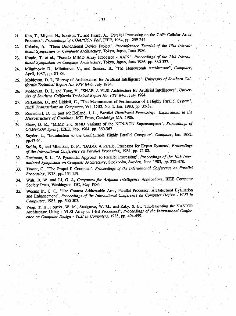
21. Kan, T., Miyata, H., Isonishi, T., and Iwase, A., "Parallel Processing on the CAP: Cellular Array Processor", Proceedings ofCOMPCON Fall, IEEE, 1984, pp. 239-244.
22. Kokubu, A., "Three Dimensional Device Project", Preconference Tutorial of the 13th International Symposium on Computer Architecture, Tokyo, Japan, June 1986.
23. Kondo, T. et al„ "Pseudo MIMD Array Processor - AAP2", Proceedings of the 13th International Symposium on Computer Architecture, Tokyo, Japan, June 1986, pp. 330-337.
24. Milutinovic D., Milutinovic V., and Soucek, B., "The Honeycomb Architecture", Computer, April, 1987, pp. 81-83.
25. Moldovan, D. I., "Survey of Architectures for Artificial Intelligence", University of Southern California Technical Report No. PPP 84-6, July 1984.
26. Moldovan, D. I., and Tung, Y., "SNAP: A VLSI Architecture for Artificial Intelligence", University of Southern California Technical Report No. PPP 84-3, July 1984.
27. Parkinson, D., and Liddell, H., "The Measurement of Performance of a Highly Parallel System", IEEE Transactions on Computers, Vol. C-32, No. 1, Jan. 1983, pp. 32-37.
28. Rumelhart, D. E. and McClelland, J. L., Parallel Distributed Processing: Explorations in the Microstructure of Cognition, MIT Press, Cambridge MA, 1986.
29. Shaw, D. E., "MIMD and SIMD Variants of the NON-VON Supercomputer", Proceedings of COMPCON Spring, IEEE, Feb. 1984, pp. 360-363.
30. Snyder, L., "Introduction to the Configurable Highly Parallel Computer", Computer, Jan. 1982, pp.47-64.
31. Stolfo, S., and Miranker, D. P., "DADO: A Parallel Processor for Expert Systems", Proceedings of the International Conference on Parallel Processing, 1984, pp. 74-82.
32. Tanimoto, S. L., "A Pyramidal Approach to Parallel Processing", Proceedings of the 10th International Symposium on Computer Architecture, Stockholm. Sweden, June 1983, pp. 372-378.
33. Timset, C., "The Propal II Computer", Proceedings of the International Conference on Parallel Processing, 1978, pp. 154-159.
34. Wah, B. W. and Li, G. J., Computers for Artificial Intelligence Applications, IEEE Computer Society Press, Washington, DC, May 1986.
35 Weems Jr., C. C„ "The Content Addressable Array Parallel Processor: Architectural Evaluation and Enhancement", Proceedings of the International Conference on Computer Design - VLSI in Computers, 1985, pp. 500-503.
36. Yeap, T. H., Loucks, W. M., Snelgrove, W. M., and Zaky, S. G„ "Implementing the VASTOR Architecture Using a VLSI Array of 1-Bit Processors", Proceedings of the International Conference on Computer Design - VLSI in Computers, 1985, pp. 494-499.

R0 R1R2D (TO NORTH, SOUTH, ERST, WEST)
2—1 MUX
C —DSGPU RESULT
ENRBLE
2-1 MUX
Yarc < 0
2-1 MUX C13
Xarc
R0-R2
C3-C5X»rc < 0 Y - Yarc
OP R
OP B
F0-F1
R0-RG3RRM
Figure l. Honeycomb ce11.

OP R OP B ~LXCR
sen
C16-C17l
NHND
Cl)I— RFQ I T
Figure 2. Honeycomb cell RLLI
MUX
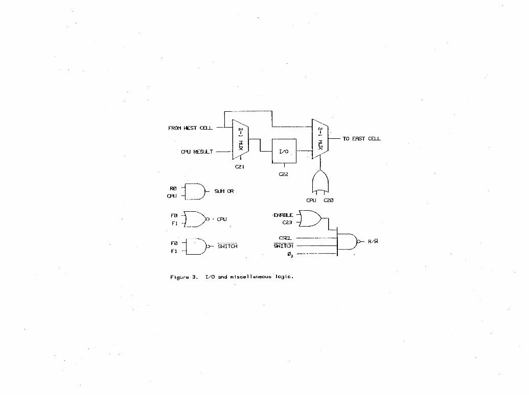
TO ERST CELLFROM WEST CELL
CPU RESULT
C22
R0 “ SUM ORCPU C20
F0FI C> CPU
F0 -| Fi
SWITCHR/W
Figure 3. I/O and miscellaneous logic.

TSW -
R14
Figure 4. Switch controllers (2 of 8).
TO NORTH CELL <TS)
SWITCH
TO NORTHERST CELL (TSW)
SWITCH

Signal Name DefinitionDN Data Signal from North CellDS Data Signal from South CellDE Data Signal from East CellDW Data Signal from West CellD Internal Data SignalTN Transmit Signal from North CellTNE Transmit Signal from Northeast CellTE Transmit Signal from East CellTSE Transmit Signal from Southeast CellTS Transmit Signal from South CellTSW Transmit Signal from Southwest CellTW Transmit Signal from West CellTNW Transmit Signal from Northwest CellA0-A2 Cell Address (x-coordinate)A3-A5 Cell Address (y-coordinate)F0-F1 Cell Function
(a)
Signal Name DefinitionC0-C2 Cell Select (x-coordinate)C3-C5 Cell Select (y-coordinate)C6-C11 RAM AddressC12 Operand SelectC13 Operand Select04 Operand Select05 Complement06-07 ALU Function08 Cany Select09 Invert CarryC20 Configuration ModeC21 I/O ModeC22 Load I/O RegisterC23 Override Enable Register
(b)
Figure 5. Signal definitions, (a) Internal signals, (b) Control signals.

Function RegistersF0 FI
Cell Mode
0 0 CPU0 1 ------1 0 Memory1 1 Switch
Figure 6. Modes of operation.
Cell Address Operand SourceY = Ysrc Xsrc < 0 West
Xsrc ^ O' EastY * Ysrc Ysrc < 0 South
Ysrc ^ 0 North
Xsrc = C0-C2 Ysrc = C3-C5
Figure 7. External operand source selection.
Cell Address Result SourceX * 0 X <0 East
X>0 West
X II o Y < 0 NorthY > 0 South
Figure 8. External result source selection.
Cell Transistor Count Percent UtilizationHoneycomb 1082CPU 832 77Memory 865 80Switch 488 45
Figure 9. Honeycomb cell efficiency.
Implementation Transistor Count Percent Utilization4K Processing Element 26,570 3864-Cell Cluster 69,248 .--
Figure 10. Processor cluster efficiency.

PI Processing Cluster
Figure 11. Extended mesh pattern embedded in honeycomb
0
• ’] SuJi tch Cell[~] Processing Cluster
(b)
Figure 12. Tree interconnection pattern, (a) Symbolic pattern, (b) Tree embedded in Honeycomb.

f~~] Processing Cluster rj Switch Cell
(b)
Figure 13. FFT interconnection pattern, (a) Symbolicpattern, (b) Pattern embedded in Honeycomb.


![Weka-STPM: a Software Architecture and Prototype for ...alvares/papers/weka_stpm_tgis2011.pdf · Weka-STPM: a Software Architecture and Prototype for ... [Bogorny et al. 2009] we](https://static.fdocuments.us/doc/165x107/5b4f3e357f8b9a2a6e8be3d1/weka-stpm-a-software-architecture-and-prototype-for-alvarespaperswekastpm.jpg)