The Graphene Handbook
95
The Graphene Handbook 1
Transcript of The Graphene Handbook
The Graphene Handbook
1

The Graphene Handbook
2
Introduction .................................................................. 3
About the author .......................................................... 4
Preface to the 2015 edition ........................................ 5
What is graphene? ....................................................... 6
Why is graphene so exciting? ........................................ 6
Graphene properties ..................................................... 6
Graphene-based materials ............................................ 7
Enabling a graphene bandgap ..................................... 15
Graphene analyzing and probing ................................ 16
On graphene’s environmental and health effects ....... 18
Graphene production .................................................. 19
Graphene applications ............................................. 24
Displays ....................................................................... 24
Conductive inks ........................................................... 25
Composite materials .................................................... 26
Coatings and paints ..................................................... 26
Electronics ................................................................... 27
Energy generation ....................................................... 28
Energy containers ........................................................ 30
Membranes .................................................................. 33
3D Printings ................................................................. 34
Sensors ......................................................................... 35
Photonics / Optics ....................................................... 36
Medicine and biology .................................................. 37
Lubricants ................................................................... 37
Spintronics ................................................................... 38
Graphene materials market .................................... 39
Graphene sheets (large area graphene) ...................... 39
Graphene flakes / GNPs .............................................. 42
Graphene oxide ............................................................ 44
Graphene ribbons ........................................................ 45
Graphene inks ............................................................. 45
Graphene composites .................................................. 46
Graphene FETs (GFETs) ............................................. 46
Market forecasts ......................................................... 48
Products with graphene on the market ................ 50
Investing in graphene ............................................... 52
Pure play graphene companies ................................... 52
Large public companies .............................................. 52
Manufacturing equipment makers ............................. 53
Graphite mining companies ........................................ 53
Indirectly investing ...................................................... 54
More options ................................................................ 54
Large graphene projects ........................................... 56
The Graphene Flagship ................................................ 56
The UK’s graphene investments .................................. 56
IBM next-gen chip material drive ............................... 56
Korea’s $40 million graphene support fund ............... 57
Main graphene challenges ....................................... 58
Mass production .......................................................... 58
Cost .............................................................................. 58
Handling ...................................................................... 58
Standardization ........................................................... 59
Bandgap enabling ........................................................ 59
Appendices ................................................................... 60
Appendix A: Glossary .................................................. 60
Appendix B: Other carbon allotropes ......................... 62
Appendix C: Other promising 2D materials ............... 66
Appendix D: Company list .......................................... 69
Table of Contents

The Graphene Handbook
3
IntroductionIn 2004, Andre Geim and Konstantin Novoselov of the University of Manchester managed to isolate graphene for the first
time ever, following their development of a simple method of isolating graphene sheets from graphite using exfoliation. The
two professors were awarded the 2010 Nobel Prize in Physics—and since then the new wonder material has sparked the
imagination of countless researchers, entrepreneurs and investors around the world.
Graphene is the world’s thinnest and strongest material, endowed with remarkable electrical, thermal and optical properties.
It’s only a single-atom thick and so is referred to as a 2D material. Graphene is also highly transparent, but is still 200 times
stronger than steel and can be flexed easily without breaking. It is said that it will take an elephant balanced on a needle point
to break through a single one-atom-thick graphene sheet!
Graphene’s myriad attributes make it a highly versatile building block, with amazing potential. The list of possible applications
is virtually endless: conductor materials (for touch displays, for example), single-molecule sensors and membranes, game-
changing battery electrodes, photodetectors, innovative composite materials, solar panels and more. Researchers have also
demonstrated graphene-based transistors, quantum dots, spintronics devices, integrated circuits and even DNA sequencers
and drug delivery agents.
Naturally, graphene also has some disadvantages. It is very difficult to produce a defect-free (pristine) graphene in volume.
Graphene also does not have an energy bandgap, which limits its usefulness for electronic devices, and some scientists are
concerned about potential health risks. Companies and researchers around the world, however, are busy developing solutions
to these problems.
Graphene is being studied by hundreds of researchers and commercial companies around the globe. This research is just at its
beginning, and every few days we hear of new developments and amazing new properties and features of graphene. Hopefully
one day we will be able to unlock for the full potential of this remarkable material!

The Graphene Handbook
4
About the authorRon Mertens is a software engineer, father and technology blogger. Ron first heard about graphene
back in 2008 while working on a new article for his
OLED-Info site, as graphene has several potential applications for the OLED industry. Ron
launched Graphene-Info in 2009 to offer resources, services and information to the graphene
industry and research community. Today Graphene-Info is considered one of the web’s top
graphene portals with tens of thousands of readers each month.
Ron lives in Herzelia, Israel and is a father to two beautiful girls. In his spare time he likes to hike,
surf, ski (which isn’t easy to do in sunny Israel), take photos, play the piano, read and evangelize
about graphene and OLED technologies.
You can find out more about Ron’s online ventures over at metalgrass.com.

The Graphene Handbook
5
Preface to the 2015 editionThe first edition of The Graphene Handbook was published toward the end of 2013. The year that passed since I wrote the
book the year that followed was a very exciting year for the graphene industry, with massive investments from the EU, UK
and private companies such as IBM, continued research into possible applications and production techniques and several new
graphene-enhanced products that entered the market.
Graphene has many challenges still ahead before it can start to fulfill its enormous potential. Mass production of high-quality
graphene sheets hasn’t been achieved yet, production capacity of graphene flakes is not even close to what may be required by
some applications and there is a clear need for more standardization.
Currently graphene is mostly used to develop new composites and enable stronger and lighter materials. We’re all waiting for
applications that use graphene’s amazing electrical, thermal and optical properties. We’ll probably have to wait a few more
years, but the future of graphene looks brighter than ever.
Here’s for a industrious 2015!
Ron MertensFebruary 2015
The Graphene Handbook
6
What is graphene?Graphene is a flat monolayer (a 2D material) that is made from carbon atoms, arranged in a hexagonal pattern (a honeycomb
crystal lattice).
Graphene is a natural material—it is the basic building block of graphite. Graphite (used in pencil tips and many industrial
applications) is simply made from stacked graphene sheets. While researchers discovered graphene back in the 1940s, it was
only in 2004 that a graphene sheet was isolated after a simple exfoliation method was discovered.
Why is graphene so exciting?Graphene has several remarkable properties. First of all, it is the thinnest material in the world (just one carbon atom thick),
and it’s also one of the strongest ones—it is much stronger than both diamond and steel of the same thickness. A graphene
sheet one square meter in size will be able to support a 4 kg cat. This graphene sheet will weigh only 0.77 milligrams (0.001%
of the weight of a 1 m2 paper sheet, or about the same weight as the cat’s whiskers).
But graphene is not just strong—it’s also flexible and transparent, it has the largest surface area of all materials, and it’s the
most stretchable crystal. The material is extremely impermeable, which means that even helium atoms cannot go through it.
Mechanically, graphene is remarkable, but that isn’t its most exciting feature. Graphene is the best electricity conductor known
to man and it is the perfect thermal conductor, too.
So it’s easy to understand why everyone is excited about this material. This simple carbon-based material is strong, light,
flexible, transparent—and it’s a great electronic and heat conductor. What more can you ask for?
Well, there is a catch, of course. Graphene is a super conductor, and it has a zero electric bandgap. This means that graphene
cannot be used to make electronic devices such as transistors. There are ways to overcome this limitation, and these will be
discussed later in the book.
Graphene propertiesGraphene has some remarkable properties—mechanical, thermal, electrical, optical and more. The following section will
list the material’s most exciting features. Note that most of these features are related to perfect graphene sheets. Defects in
graphene (some of them are made from several smaller flakes “stitched together,” for example) can make graphene weaker
and with quite different properties.
Physical / MechanicalGraphene is the world’s thinnest material—it is only one carbon atom thick (around 0.34 nm). It is also the world’s toughest
2D material—much harder than either steel or diamond of same dimensions. Graphene has a tensile strength (the maximum
stress that a material can withstand while being stretched or pulled before failing or breaking) of over 1 Tpa. There is only one
material that may be stronger than graphene—carbyne, which is a string of carbon atoms, basically a one-atom wide graphene
ribbon. (Carbyne is very difficult to synthesize, though.)

The Graphene Handbook
7
Graphene is light—it weighs just 0.77 milligrams per square meter. Because it is a single 2D sheet, it has the highest surface
area of all materials. When left to themselves graphene sheets will stack and form graphite, which is the most stable 3D form
of carbon under normal conditions.
Graphene sheets are flexible, and in fact graphene is the most stretchable crystal—you can stretch it up to 20% of its initial size
without breaking it. Finally, a perfect graphene is also highly impermeable, and even helium atoms cannot go through it.
Electronic propertiesGraphene is the material with the highest electrical current density (a million times that of copper) and the highest intrinsic
mobility (100 times that of silicon). Graphene has a lower resistivity than any other known materials at room temperature,
including silver. And there are some methods to turn it into a superconductor (it can carry electricity with 100% efficiency).
While all this makes graphene the fastest and most efficient conductor, it cannot be readily used to make transistors as it does
not have a bandgap. There are several methods to open a bandgap, however, and these will be detailed later in this book.
Thermal conductivityGraphene is the perfect thermal conductor - it features record thermal conductivity—much higher than carbon nanotubes,
graphite and diamond (over 5,000 W/m/K). Graphene conducts heat in all directions - it is an isotropic conductor.
Optical propertiesGraphene is extremely thin, but it is still a visible material, as it absorbs about 2.3% of white light (which is actually quite a lot
for a 2D material). Combine this with graphene’s amazing electronic properties, and it turns out that graphene can be used to
make very efficient solar cells.
Of course, absorbing 2.3% of visible light still makes graphene very much transparent to the human eye; it can be used to make
transparent conductors, for example.
Chemical propertiesDespite the fact that all of graphene’s atoms are exposed, it is an inert material and does not readily react with other atoms.
Graphene can, however, “absorb” different atoms and molecules. This can lead to changes in the electronic properties, and
may also be used to make sensors or other applications.
Graphene can also be functionalized by several chemical groups, which can result in different materials such as graphene oxide
(functionalized with oxygen and helium) or fluorinated graphene (functionalized with fluorine). These will be discussed later
in the book.
Graphene-based materialsWhen I discussed graphene above, I was referring to a graphene sheet—a single layer of carbon atoms in a perfect honeycomb
lattice. The term graphene, however, is used to describe a family of materials that are derived in all sorts of ways from the
basic graphene sheet.
The Graphene Handbook
8
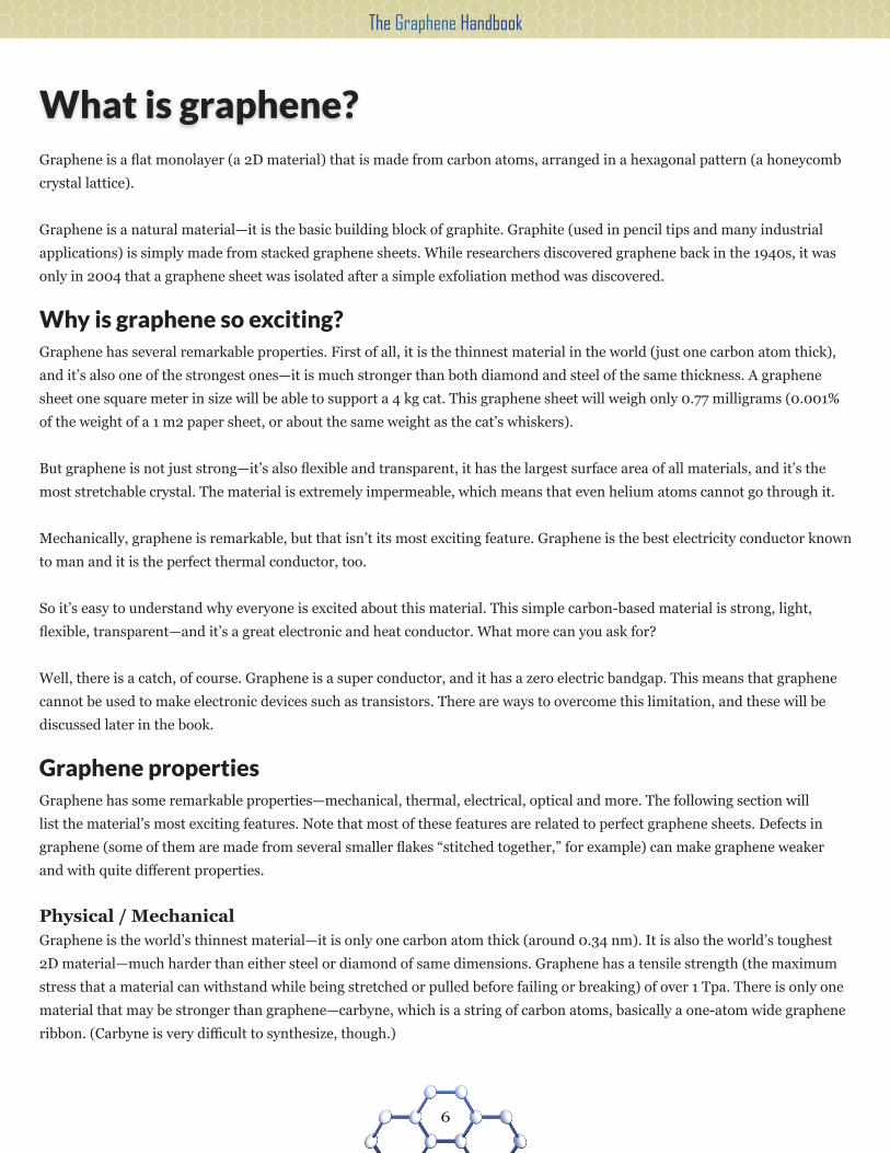
Monolayer to 3D graphene, and in betweenA single 2D sheet of carbons in a honeycomb lattice is called graphene. If you stack many such sheets on top of each other you
get graphite. Graphite is a natural mineral that has been mined and used for centuries. If you combine it with clay, you get
pencil “lead” for example. It is also used to make battery anodes and has many uses in industry.
Graphene, Graphite, CNTs and Buckyballs (credit: Andre Geim)
If you stack two sheets of graphene one on top of the other, you get bilayer graphene. It turns out that this material differs
from monolayer graphene in its electrical properties. Just like graphene, it has a zero bandgap, but a controllable bandgap can
be introduced by applying an electric displacement field to the two layers. A bandgap can also be introduced by stacking the
two layers in a unique arrangement. Bilayer graphene can also be used to make ultra-fast broad-range photodetectors.
Three (trilayer) or more sheets of graphene can be used to create materials These are referred to collectively as “few-layer
graphene.” When you reach about ten layers, the properties start to resemble graphite, so we’ll use few-layer graphene to
describe graphene stacks with up to ten sheet layers.
Graphene may also be regarded as the basic planar carbon lattice that can be the basis of 3D curved objects—such as fullerenes
(buckyballs) and carbon nanotubes. These materials will be discussed in the appendices.
Graphene Nanoribbons (GNRs)Graphene Nanoribbons (GNRs, sometimes referred to as graphene nanowires) are thin (under 50 nm) strips of graphene (and
so some refer to them as 1D graphene). These ribbons have interesting electronic properties, which depend on the width and
The Graphene Handbook
9
edge type of the material. In fact, GNRs can be metals, semiconductors, halfmetals, feromomagnets and antiferomagnets—
depending on the width, shape, edge structures and chemical termination. Basically GNRs are semiconductors with an energy
gap that scales (inversely) with the width of the ribbon.
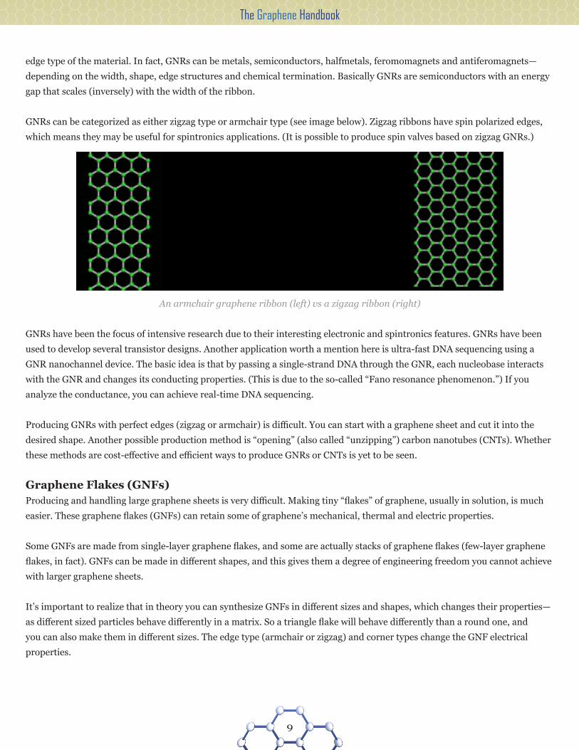
GNRs can be categorized as either zigzag type or armchair type (see image below). Zigzag ribbons have spin polarized edges,
which means they may be useful for spintronics applications. (It is possible to produce spin valves based on zigzag GNRs.)
An armchair graphene ribbon (left) vs a zigzag ribbon (right)
GNRs have been the focus of intensive research due to their interesting electronic and spintronics features. GNRs have been
used to develop several transistor designs. Another application worth a mention here is ultra-fast DNA sequencing using a
GNR nanochannel device. The basic idea is that by passing a single-strand DNA through the GNR, each nucleobase interacts
with the GNR and changes its conducting properties. (This is due to the so-called “Fano resonance phenomenon.”) If you
analyze the conductance, you can achieve real-time DNA sequencing.
Producing GNRs with perfect edges (zigzag or armchair) is difficult. You can start with a graphene sheet and cut it into the
desired shape. Another possible production method is “opening” (also called “unzipping”) carbon nanotubes (CNTs). Whether
these methods are cost-effective and efficient ways to produce GNRs or CNTs is yet to be seen.
Graphene Flakes (GNFs)Producing and handling large graphene sheets is very difficult. Making tiny “flakes” of graphene, usually in solution, is much
easier. These graphene flakes (GNFs) can retain some of graphene’s mechanical, thermal and electric properties.
Some GNFs are made from single-layer graphene flakes, and some are actually stacks of graphene flakes (few-layer graphene
flakes, in fact). GNFs can be made in different shapes, and this gives them a degree of engineering freedom you cannot achieve
with larger graphene sheets.
It’s important to realize that in theory you can synthesize GNFs in different sizes and shapes, which changes their properties—
as different sized particles behave differently in a matrix. So a triangle flake will behave differently than a round one, and
you can also make them in different sizes. The edge type (armchair or zigzag) and corner types change the GNF electrical
properties.
The Graphene Handbook
10
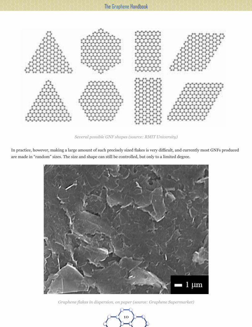
Several possible GNF shapes (source: RMIT University)
In practice, however, making a large amount of such precisely sized flakes is very difficult, and currently most GNFs produced
are made in “random” sizes. The size and shape can still be controlled, but only to a limited degree.
Graphene flakes in dispersion, on paper (source: Graphene Supermarket)

The Graphene Handbook
11
Graphene Nanoplatelets (GNPs)A nanoplatelet is a small round disk-shaped particle (hence with a shape like a plate). In theory, graphene nanoplatelets are
disk-shaped graphene sheets (or stacks of sheets). So a GNP is a type of graphene flake.
In practice, however, as was mentioned in the previous section, it is very difficult to create round-shaped graphene platelets—
even if they are artificially synthesized. Some GNFs are marketed as GNPs, even though they are not disk-shaped.
As some of these GNPs are made from stacks of few-layered graphene, they are also sometimes referred to as graphite
nanoplatelets.
xGNPs—graphene nanoplatelets (credit: XG Sciences)
One of the leading companies offering GNPs is XG Sciences, and their product line helps explain the previous point. XG
Sciences offers several types of GNPs (branded as xGNPs) and grades them by average thickness. They offer three grades, from
1 nanometer (about three layers on average) to about 14 nanometers (about 38 layers, so this should really be called graphite
nanoplatelets). The lateral dimensions of xGNPS range from 1 micron to 50 microns.
Graphene Quantum Dots (GQDs)A quantum dot (QD) is a tiny semiconductor that has electronic properties between those of bulk semiconductors and of
discrete molecules. QDs are being studied for several applications (including transistors, PV cells, LEDs and even quantum
computing) and are recently being adopted in some displays and LED devices.
The Graphene Handbook
12
The size and shape of the quantum dot control its electronic characteristic. So, for example, if you use a QD to emit light in a
LED-like application, the size may change the color (wavelength) of the emitter light. The dot’s size and bandgap are inversely
related.
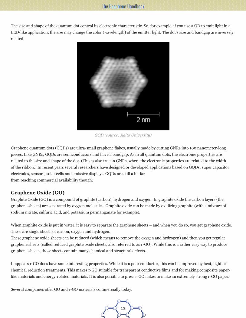
GQD (source: Aalto University)
Graphene quantum dots (GQDs) are ultra-small graphene flakes, usually made by cutting GNRs into 100 nanometer-long
pieces. Like GNRs, GQDs are semiconductors and have a bandgap. As in all quantum dots, the electronic properties are
related to the size and shape of the dot. (This is also true in GNRs, where the electronic properties are related to the width
of the ribbon.) In recent years several researchers have designed or developed applications based on GQDs: super capacitor
electrodes, sensors, solar cells and emissive displays. GQDs are still a bit far
from reaching commercial availability though.
Graphene Oxide (GO)Graphite Oxide (GO) is a compound of graphite (carbon), hydrogen and oxygen. In graphite oxide the carbon layers (the
graphene sheets) are separated by oxygen molecules. Graphite oxide can be made by oxidizing graphite (with a mixture of
sodium nitrate, sulfuric acid, and potassium permanganate for example).
When graphite oxide is put in water, it is easy to separate the graphene sheets – and when you do so, you get graphene oxide.
These are single sheets of carbon, oxygen and hydrogen.
These graphene oxide sheets can be reduced (which means to remove the oxygen and hydrogen) and then you get regular
graphene sheets (called reduced graphite oxide sheets, also referred to as r-GO). While this is a rather easy way to produce
graphene sheets, those sheets contain many chemical and structural defects.
It appears r-GO does have some interesting properties. While it is a poor conductor, this can be improved by heat, light or
chemical reduction treatments. This makes r-GO suitable for transparent conductive films and for making composite paper-
like materials and energy-related materials. It is also possible to press r-GO flakes to make an extremely strong r-GO paper.
Several companies offer GO and r-GO materials commercially today.

The Graphene Handbook
13
Graphene compositesGraphene (or graphene flakes, GNPs and GNRs) can be stacked or combined with other materials to create composite (hybrid)
materials. Composite materials offer a set of features or properties suitable for specific applications, and may be more cost-
effective than “pure” materials.
The most simple and common composites are made by adding small amounts of graphene to metals, polymers or ceramics.
Graphene can make these materials stronger, more conductive and more heat resistant. It was found that adding just 0.22%
of graphene to alumina makes it 50% more resistant to the propagation of cracks under strain, while electrical conductivity
increased by a factor of a hundred million.
Another example of a composite material is a silicon-graphene lithium-ion battery anode developed at Northwestern
University. It was reported that this anode increases energy density by three times and anode capacity by four times compared
to existing materials. This composite material is now being commercialized by CalBattery, which plans to bring it to market in
2015.
A more recent example is MIT’s research into next-gen solar cells, attempting to find the “ultimate power conversion device”.
The researchers developed a bilayer material made from a graphene sheet on top of a molybdenum disulfide sheet. For the
same weight, the new material will enable PVs that are 1,000 times more efficient than silicon-based panels. A single bilayer
material will only achieve 1% to 2% efficiency, but hopefully it will be possible to stack several layers, which will boost the
efficiency dramatically. The two layers together are just 1 nm thick—silicon PVs are hundreds of thousands times thicker.
Graphene dopingDoping is a process in which you introduce “impurities” into a pure material, usually to change its electrical properties.
Graphene doping involves replacing some of the carbon atoms with other atoms. One of the prime examples is the
introduction of an energy bandgap into graphene by doping.
The most common atoms used to dope graphene are silicon, nitrogen, boron and sulfur. Boron (B) and nitrogen (N) are
natural candidates for graphene doping, as their atomic size is similar to graphene’s carbon atoms. Replacing atoms is
sometimes referred to as hetero doping or substitutional doping.
There are other kinds of doping possible with graphene. Some researchers are working toward chemical modification of
graphene, by using NO2 or NH3 molecules, for example. Again, such doping enables the opening of a bandgap and altering
other properties.
Graphene substrates (handling graphene)A graphene sheet is thin (in fact, it’s the thinnest material in the world), and handling it isn’t easy, to say the least. Graphene
sheets are produced on different substrates, and sometimes they are transferred to other substrates following their production.

The Graphene Handbook
14
Graphene on copper foil (source: Graphene Supermarket)
Graphene sheets are usually made on silicon (or SiO2) substrates, and sometimes on copper, nickel, flexible polymers and
other substrates. Some companies offer graphene on any substrate (you send the substrate, they will return it with a graphene
sheet on top).
Handling graphene flakes (GNFs) is also somewhat of an issue. It’s possible to get the flakes in dry powder, but this can be
problematic and hazardous. It’s more common to buy GNFs in solution (water, resins, organic solutions, etc.).
Graphene functionalizationWhen you functionalize a material, you add functional groups on the surface of the material to achieve desired surface
properties (such as water repellent coating or changing the color by attaching chromophores). Functionalization of graphene
has several advantages. First of all, it may enable new materials (these are classified, sometimes, as “surface modified
graphenes”) that can be used in a wide range of applications (for example, drug delivery and transistors). Secondly, it enables
the dispersion of graphene (or GNFs) in solutions and enables solution-based production processes. Finally, it can alter
graphene’s electrical properties (and open a bandgap).
Functionalization can be achieved in two ways. The first (and more straightforward) one is covalent bonding of organic
functional groups. There are two main alternatives here. You can start with graphene and form covalent bonds to the C=C
bonds, or start with graphene oxide and form the bonds to the oxygen groups. As was mentioned above, this functionalization
method can be used to enable the dispersion of graphene in organic solvents, to change graphene’s properties or to open a
bandgap.
One useful covalent functionalization is the attachment of graphene oxide to polymers. In this case the polymers provide the
basic mechanical and morphological characteristics, while the graphene adds electrical conductivity and chemical reactivity
and may make the final material even stronger.
Covalent functionalization has resulted in several promising new materials. When you use covalent functionalization and add

The Graphene Handbook
15
hydrogen (H) atoms to graphene (basically “terminating” the edge C atoms with H atoms), you create a new material which
is called graphane. Graphane was first developed at the University of Manchester in 2009. Graphane was synthesized by the
exposure of graphene to cold hydrogen plasma. This material is similar to graphene, but it acts as an insulator. It is thought to
be the ideal insulator material that can combine with graphene to create integrated electronic devices or sensors. No one has
managed to actually connect these two materials together, though.
Another interesting material was developed by the fluorination of graphene. The resulting material, fluorographene (or
graphene fluoride) was synthesized by fluorination of graphene using XeF2 at room temperature. Similar to graphane,
fluorographene is an insulator. It also has some interesting optical properties.
The second functionalization method is the noncovalent type. This is a promising way to enable the dispersion of graphite in
solvents and create monolayer graphene sheets (avoiding stacking). It can also lead to interesting new graphene properties.
So-called graphene-ligand functionalization could lead to interesting applications such as hydrogen storage by hydrogen
physisorption on graphene sheets. Graphene and nucleobases have been used to design a fast 2D DNA sequencing device.
Graphene as a substrate for nanoparticlesIf we consider a large graphene sheet, then it is possible to place nanoparticles on top of graphene. This is a sort of
functionalization that can lead to interesting results. A perfect graphene sheet is considered the ideal substrate—it has the
largest possible surface area per volume, and it is highly conductive, light and strong.
Dispersion of metal nanoparticles on graphene has been studied by several researchers, with an aim to produce materials
useful for catalytic, magnetic and optoelectronic applications. One promising application, for example, is anode materials
for Li-Ion batteries. Another promising device is graphene with quantum dot (QD) particles on top. Graphene is an efficient
charge transfer for the QDs—useful in solar cells, displays, lighting and other applications.
In September 2014 IBM announced a new method to use graphene as a substrate for single-crystalline semiconductor film
growth. Graphene will be less expensive than current single-crystalline wafers used in such production methods, as it can be
reused indefinitely.
Enabling a graphene bandgapAs was discussed before, graphene has excellent electronic properties, but it does not have a bandgap. In fact, this zero
bandgap is what makes graphene such an excellent conductor. But sometimes a bandgap is useful, and there are several ways
to enable a bandgap in graphene.
But first of all, it’s important to understand just what a bandgap is and why it is important. The bandgap (also called the
energy gap) is an energy range in which no electron states can exist. This energy range also represents the amount of energy
it requires to free an electron—to become a mobile charge carrier. So a material with a low bandgap is a conductor, while a
material with a large bandgap is an insulator.
A semiconductor has a conductivity that’s between a conductor and an insulator. And correspondingly, its bandgap is not large
and not small. A semiconductor is the basic building block of modern electronics, so obviously the ability to turn graphene into
a semiconductor (by enabling a large enough bandgap, but not too large) is important.

The Graphene Handbook
16
Silicon (and other insulating materials such as germanium and, yes, carbon) is usually turned into a semiconductor by doping.
There are two types of doping, N-doping (which adds extra electrons) and P-doping (which introduces electron “holes”), which
turns it into a p-type or n-type material.
Doping is also possible in graphene, and indeed this is one of the ways to enable a bandgap. Doping was discussed before—
basically the idea is to introduce non-carbon atoms (usually silicon, nitrogen, boron and sulfur), and this opens up a bandgap.
It turns out that if you make small graphene flakes (GNFs) or nanoribbons (GNRs), these materials intrinsically have a
bandgap. This is because the carbon atoms at the edge of the material are not all connected to other carbon atoms like those in
the middle of the sheet. So another way to enable a bandgap is simply to use a graphene ribbon or small flake.
Another way to enable a non-zero bandgap is to stack two layers of graphene together in a unique arrangement. In addition, if
you take a normal bilayer graphene and apply an electric displacement field, you create a controllable bandgap.
Finally, in August 2013 it was demonstrated that it is also possible to build graphene-based transistors without introducing
a bandgap. In what may prove to be a groundbreaking work, researchers from the University of California Riverside used
graphene’s negative resistance to build logic gates from several regular graphene field-effect transistors (GFETs). Those gates
are smaller and faster than silicon-based gates—by orders of magnitude (for example, they can operate at over 400 Ghz).
Graphene analyzing and probingOne of the problems with graphene is that it is a difficult material to analyze and probe. There are several methods to view and
analyze a graphene sheet (or other graphene-related materials such as GNFs and GNRs).
Scientists sometimes adjust or alter an existing method to better suit their exact needs, and it is important to know and
understand these methods. Of course, these tools are also useful for graphene makers to monitor and improve production
quality.
Scanning Electron Microscopy (SEM)A scanning electron microscope sends a focused beam of electrons to interact with the sample. The interaction between
the electrons and the sample creates all sorts of signals that can be detected. SEM can achieve a resolution higher than 1
nanometer.
Graphene film on copper (SEM source: Graphene Supermarket)

The Graphene Handbook
17
SEM is useful in understanding the sample surface topography and composition in all sorts of conditions (dry, wet, vacuum,
etc.).
Transmission Electron Microscopy (TEM)Like SEM, TEM microscopy uses a beam of electrons. But here the electrons are transmitted through a sample (which has
to be ultra-thin, so obviously graphene fits). Some of the electrons pass through the sample—and these are the parts that are
illuminated in the image.
Graphene film TEM (source: University of Washington)
Atomic Force Microscopy (AFM)Atomic force microscopy, as its name suggests, uses a mechanical probe (or tip) to touch a sample and gather information. It
can also gather electrical information (such as the conductivity of the sample).
AFM images of graphene (left) and graphene oxide (right) (source: Agilent)

The Graphene Handbook
18
AFM is very accurate, and its resolution can be a fraction of a nanometer. It can measure contact force, chemical bonding,
electrostatic forces, magnetic forces, etc.
Incidentally, graphene has been proven to be an excellent coating for AFM tips. The graphene coating makes the microscope
tip conductive and more resistant to wear.
Raman spectroscopy Raman spectroscopy uses a laser light to interact with molecular vibration (or other excitations) in a sample to gather
vibrational modes. Raman spectroscopy takes advantage of Raman scattering (the inelastic scattering of a photon) to detect
low-frequency modes. The information gathered from such an analysis can be used to identify molecules or study changes in
chemical bonding.
Raman imaging of single layer and multilayer graphene (source: Nanophoton)
Raman spectroscopy is an important tool for graphene research. It can be used to ascertain the number of layers (thickness)
and the chemical and physical properties of graphene. It can also be used to study the edges of graphene materials and the
effects of graphene doping and functionalization.
On graphene’s environmental and health effectsGraphene is a wonder material, but some researchers are worried about health and environmental risks. This section
summarizes some of the latest findings regarding graphene risks.
Graphene was found to be harmful for bacteria, because of several mechanisms. Researchers from Singapore discovered
in 2012 that when graphene directly contacts bacteria it can kill them, because the graphene causes membrane stress and
irreversible damage. Newer research in 2013 demonstrated that graphene can kill bacteria by slicing through their membrane
and pulling out the phospholipids.
The fact that graphene can damage bacteria may actually be positive, as it can be used as a basis for antibacterial materials (for
example, a graphene-based band-aid). Graphene may also be used to build biosensors that can detect bacteria. Researchers
from China have discovered that magnetic reduced graphene oxide can rapidly kill bacteria, using several mechanisms
(oxidative stress, physical piercing and photothermal heating).

The Graphene Handbook
19
Graphene may also pose health risks for humans. Like many other nanoparticles, inhaled graphene flakes could damage your
lungs. This means that graphene production environments may be risky. We still do not know enough about graphene and its
effects.
Regarding graphene’s environmental effects: basically graphene is made from just carbon atoms, so it does not contain any
rare or harmful materials. On the other hand, graphene production may involve using chemicals or a lot of energy—but, of
course, as we haven’t reached mass production yet it is too early to understand the total cost of graphene production.
There has been a lot of research using graphene as a way to enable highly efficient energy harvesting, energy generation and
energy storage devices. Graphene is even a promising potential material for water desalination and purification devices. So
graphene may be one of the key enablers for clean energy and water technologies and may help to clean up and preserve our
planet.
Graphene productionBasically there are two ways to produce graphene or graphene-related materials (GNFs, GNRs, etc.). The first one is top-
down, which means you begin with graphite (or other carbon materials) and produce graphene—using exfoliation (peeling),
reduction (for example, turning graphene oxide into graphene), unzipping graphene nanotubes, intercalation or other
methods. The second way to produce graphene is bottom-up: start with carbon in some form and synthesize the graphene
sheets or flakes.
There are dozens of possible methods of producing graphene currently being researched in academia and used by different
companies. Some of these methods are used to produce large pristine graphene sheets (no one has achieved mass production
yet, though) while others are used to create graphene flakes of various morphologies and qualities.
GNFs and GNRs production is more advanced compared to graphene sheet production. Some companies are already
producing GNFs, and the production capacity of these companies is usually a few tons of material per year. For example,
XG Sciences, a leading GNF provider, currently has a facility that can produce 80 tons per year. This is still far from enough,
though. The market for Li-Ion anode material (just one out of many possible GNF applications) is currently estimated at
50,000 tons per year, and it is expected to grow quickly as electric vehicles start to enter the market.
The following sections will present several specific ways to produce graphene. Most of these methods cannot produce 100%
perfect graphene sheets, and the properties of the materials produced change from method to method (due to size, defect
nature, substrate, etc.).
Graphite exfoliationWhen Andre Geim and Konstantin Novoselov managed to isolate graphene sheets in 2004 for the first time, they used
micromechanical exfoliation. This only sounds complicated—what they did was to simply use scotch tape to peel a layer of
graphite from a large graphite block and then repeatedly use more scotch tape to make that layer thinner and thinner. If you
do this enough times you get graphene.
Micromechanical exfoliation can also be used in industrial-scale graphene production, using several techniques. There are

The Graphene Handbook
20
other possible exfoliation methods, including chemical exfoliation, sonficiation (applying sound energy) and more.
Graphene intercalationIntercalation means the insertion of molecules (or ions) into compounds with layered structures, which are then used to pull
out a single sheet. Intercalation can be considered to be an exfoliation method, and it can be used to produce graphene from
graphite.
Graphene intercalation was first attempted in 1841 (!) but only recently researchers managed to develop intercalation
methods that do not damage the resulting sheets. As far as we know, there is no commercial graphene production based on
intercalation.
Graphene synthesisSynthesizing graphene (or GNFs) means to build the materials atom-by-atom, bottom up. Synthesis can take many forms, and
one of the most common ways to produce graphene sheets today is CVD, which is a synthesis method. CVD will be discussed in
the next section, and the following section will discuss MBE, a similar method.
There are other synthesis methods besides CVD and MBE, though, that can be used to produce graphene. Graphene
Technologies, for example, developed (and patented) a unique process that synthesizes graphene atom-by-atom from CO2.
They start the process with feedstock (a renewable, biological material) and use it to oxidize magnesium at high temperatures.
This process creates bulk volumes of pristine, few-layer graphene flakes.
Chemical Vapor Deposition (CVD)CVD (Chemical Vapor Deposition) is a process which deposits a material in gas form on a substrate in a closed chamber.
Basically it’s a simple process: you combine your material with a carrier gas, release it in a chamber, and some of it lands on
the substrate to create a thin film. There are many types of CVD processes used in several industries to produce thin-film
materials on all sorts of substrates.
A compact CVD system (credit: Moorfield)

The Graphene Handbook
21
CVD processes are usually slow and so can be tuned to create the desired thickness. (On average CVD creates a micron-thick
film in about an hour.) CVD usually results in very high quality films (although this isn’t always true for graphene) and is
relatively cheap. One major disadvantage of CVD, though, is the highly toxic gaseous by-products. It is also q wafeul process.
CVD is being used in many universities and companies to produce graphene sheets; however, no one has yet managed to
mass produce graphene using CVD. One of the major issues is the separation (exfoliation) of the graphene from the substrate.
It turns out this isn’t as easy as with other CVD-grown materials (so this turns into a costly and slow procedure). CVD also
requires very high temperatures, and another issue is that it is difficult to achieve a uniform graphene sheet using CVD.
Despite these issues, several companies are already offering CVD-grown graphene sheets on a variety of substrates. These
graphene sheets are very expensive, though—a one-square-centimeter of high quality graphene may cost hundreds of dollars.
CVD graphene is usually grown on copper, but it’s possible to transfer it to any substrate.
Molecular Beam Epitaxy (MBE)MBE is quite similar to CVD. In MBE, you heat elements in a high vacuum chamber until they slowly begin to sublime. The
gaseous elements then condense on the substrate. The atoms do not interact with each other or other chamber gases until they
reach the substrate (due to the long mean free path).
Graphene MBE equipment (source: Argonne National Laboratory)

The Graphene Handbook
22
MBE does not require a very high temperature for graphene deposition—around 300 degrees Celsius. (CVD usually requires
600 to 1,000 degrees.) MBE systems are used to deposit all sorts of materials such as single-crystal gallium arsenide, organic
semiconductors and more.
Currently MBE systems are used to produce graphene sheets in research labs, but as far as we know there isn’t any commercial
graphene production performed using MBE.
GO reductionA reduction is a chemical process that results in a decrease in oxidation number. Basically it means losing oxygen atoms—
either by gaining electrons or hydrogen atoms. So one possible way to produce graphene is the reduction of oxidized graphene
/ graphite.
Basically the idea here is to oxidize graphite (which is simple, using a mixture of sodium nitrate, sulfuric acid and potassium
permanganate). This results in graphene oxide (GO). GO differs from graphene in most traits, but it has its own unique uses.
Single layers of GO can also be reduced to get graphene sheets.
The main problem with GO reduction is that the quality of the graphene is very poor, as it contains many chemical and
structural defects. The reduced graphene is referred to as reduced GO (or r-GO). While this is not high-quality graphene it is
still useful, and several companies are offering such materials.
In 2012 researchers from UCLA developed an interesting method to produce r-GO using consumer DVD burners. They
deposited GO on blank DVDs and then used the DVD laser (infrared 780 nm) to reduce the material. The researchers have also
developed an application for this so-called laser-scribed-graphene (LSG)— supercapacitor electrodes. This is not a gimmick
process—it can be scaled for volume production, and those electrodes have appealing features. We do not know whether this
technology is approaching commercialization.
Laser scribed graphene on DVD media (source: UCLA)

The Graphene Handbook
23
Unzipping carbon nanotubesOne interesting way to produce graphene nanoribbons (NGRs) is to open (or unzip) carbon nanotubes (CNTs). This process
can be done chemically—for example, potassium permanganate and sulfuric acid cut open CNTs in solution. Another
possibility is to use plasma etching to open CNTs embedded in a polymer film.
Of course, this method relies on having a cheap way to produce high-quality CNTs. You can read more about CNTs in the
appendices.
Proprietary production methodsThere are many other ways to produce graphene. Many companies and research institutes are trying out different ways, as
no one has achieved mass production of low-cost graphene yet. These companies promise low-cost, environmentally friendly
production, but sadly most of them keep the actual process details under wraps. Many of these processes are modified
exfoliation, CVD or MBE processes.
The Graphene Handbook
24
Graphene applicationsGraphene is a basic material with amazing mechanical and electric properties. As such, it is suitable for use in a wide range
of applications. This chapter will list the most popular graphene applications currently being researched, developed and
commercialized.
DisplaysSome people believe that the first application to adopt graphene in volume will be conductive wires for transparent touch
panels. Currently most touch panels (used mostly in mobile phones and tablets) use indium tin oxide (ITO). ITO is useful
because it is conductive and transparent, but the supply is limited (even though companies are now harvesting ITO from
recycled electronic devices) and it’s also brittle (so it’s not suitable for flexible panels), so companies are looking for
alternatives. Graphene is transparent, flexible and highly conductive, and so may be an excellent candidate to replace ITO,
especially for flexible displays.
Several companies are working toward graphene-based touch panels. Back in 2013, Shanghai’s Powerbooster claimed they
already produce millions of graphene-based films each month, supplying them to Chongqing Morsh Technology who will use
them to produce 15” transparent conductive films. The original plan was to begin volume production by March 2014, we’re not
sure what the current status of this project is.
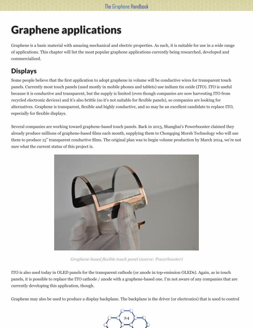
Graphene-based flexible touch panel (source: Powerbooster)
ITO is also used today in OLED panels for the transparent cathode (or anode in top-emission OLEDs). Again, as in touch
panels, it is possible to replace the ITO cathode / anode with a graphene-based one. I’m not aware of any companies that are
currently developing this application, though.
Graphene may also be used to produce a display backplane. The backplane is the driver (or electronics) that is used to control

The Graphene Handbook
25
which pixels are on and which are off in a display. Currently most displays (whether LCD, e-paper or OLED) use amorphous
silicon (a-Si), polysilicon (LTPS) or oxide-TFTs. Graphene will enable flexible, transparent and highly conductive backplanes.
Some companies are already developing such solutions. In July 2013 Plastic Logic entered into a partnership with the
University of Cambridge to co-develop graphene-based flexible plastic display backplanes, and in September 2014 Plastic
Logic demonstrated the world’s first display with a graphene backplane (a flexible E Ink panel).
Conductive inksMost conductive inks today are made from either silver or carbon-based materials. Conductive inks are used in a wide variety
of applications such as RFID tags, heating elements (in car windshields, for example), biosensors, computer keyboards and
touch screens.
Graphene, with its high conductivity, is a good choice for the conductive elements in the ink. Several companies are working
on graphene-based inks, and some already offer commercial products.
Rolls of printed graphene electronics (source: Vorbeck Materials)
The first company to commercialize graphene inks was Vorbeck Materials, with their Vor-ink family of conductive inks. In
2012 MWT Packaging announced the first product to use these inks: the Siren Technology security smart packaging (an
electronic article surveillance system), which is used to identify items in retail stores when they pass through a gate. Each
Siren tag includes a fully integrated conductive circuit made from graphene. Reportedly these tags, which can be flexed and
wrinkled without damage to the circuit, feature excellent conductivity at a competitive price—in fact, Vorbeck claims that their
inks offer ten times the conductivity of silver inks. MWV uses flexographic roll-to-roll printing to process Vorbeck’s Vor-Ink
Flexo at 60 m/min.
Another company that offers graphene-based inks is UK’s Haydale (a subsidiary of the ICL Group). In June 2013 the company
announced the availability of their HDPlas Graphene Ink Sc213. These inks have been optimized for ideal viscosity and
solid contents, ensuring excellent coverage and exceptional conductivity. UK-based Perpetuus Carbon Technologies is also

The Graphene Handbook
26
offering a graphene-based ink that features a resistance below one ohm per square centimeter. Perpetuus says this is the most
conductive graphene enabled ink in the world, and it is available in formulations for ink jet, flexographic printing and sensors
technologies.
Composite materialsGraphene can be used to enhance all sorts of materials and create so-called “composite materials.” Adding graphene (flakes, in
most cases) to materials may enhance the mechanical, thermal and electrical properties. Even tiny amounts of graphene can
make the matrix material lighter, stronger and more conductive for both heat and electricity.
Composite materials are one of the most promising applications for graphene, and there is a tremendous amount of
applications that can benefit from graphene composites. Many companies are developing such materials, and many others are
developing specific applications for those materials. Promising matrix materials include plastics, rubber, epoxy resins, metals
and carbon fibers.
Graphene composite materials are already available in the market. The sports equipment market was one of the first to
embrace graphene, and there are already tennis rackets, cycling helmets and shoes and cycling wheels – all using graphene
composites (usually graphene combined with carbon fibers).
Coatings and paintsGraphene is extremely impermeable—even helium atoms cannot go through it. Graphene is also hydrophobic, which means
it repels water. This makes graphene an interesting material for developing coating materials that can be used to protect from
oxygen, moisture, corrosion and other environmental hazards. Because graphene is transparent, it can be useful in many
coating applications.
Spanish Graphenano is offering a graphene based paint called Graphenstone. This paint is reportedly super strong and it
also acts as a protective layer against environmental damage. Graphenstone is made from a graphene powder and limestone
powder. Graphenano is producing this paint in industrial quantities.
Rice University researchers discovered that graphene coating on copper makes it almost 100 times more resistant to corrosion.

The Graphene Handbook
27
Graphene is an excellent anti-corrosion coating material and has been proven to be the world’s thinnest corrosion-protecting
metal coating. In another research conducted at Rice, it was discovered that adding graphene ribbons to a polymer material
(TPU) makes it more impermeable to pressurized gas—it is a thousand times harder for gas molecules to escape through the
polymer after adding GNRs. This could lead to much lighter gas tanks used in automobiles, soda bottles and even beer.
ElectronicsGraphene, as the world’s most conductive material, has an exciting potential in the electronics industry. Some people believe
that graphene will be the “next silicon” and that it will revolutionize our computers and chips. But it will take some time before
we’ll see major commercialization of graphene-based electronics.
Graphene FETs (source: Bluestone Global Tech)
As was discussed earlier in the book, graphene does not have a bandgap. This means that it cannot be used to make
transistors. However, there are many ways to open a bandgap in graphene—by using graphene ribbons, doping it, using bi-
layer graphene and more. It is also possible to build logic gates using graphene based on negative resistance, without opening
a bandgap.
Most of the activity in graphene-based electronics is currently done at universities and research institutes and in large
corporations (such as IBM, Intel and Samsung). In past years we’ve seen several graphene-based transistor designs and also
some applications in memory, displays drivers and RF integrated circuits. It seems that most designs use graphene ribbons
(GNRs), as those have a bandgap. In the following paragraphs we’ll detail some of the latest research.
In July 2014, IBM announced a new $3 billion five-year research initiative with an aim to find the next-generation chip
technology to replace silicon. IBM will look into graphene, carbon nanotubes, quantum computing, silicon photonics and more
technologies. Intel is also looking at graphene transistors, and in the best case scenario Intel sees graphene-based products
emerging in 2019.

The Graphene Handbook
28
In March 2013 researchers from Switzerland’s EPFL designed a new flash memory cell prototype that is made from graphene
and molybdenite (MoS2). The new design is efficient, flexible, small and fast. It combines the good electronic properties of
MoS2 with graphene’s excellent conductivity.
As was mentioned before, researchers from the University of California, Riverside developed a graphene-based transistor
based on negative resistance rather than trying to open up a bandgap. Negative resistance is the counterintuitive phenomenon
in which a current entering a material causes the voltage across it to drop. The researchers showed how an array of several
graphene FETs can be manipulated to produce conventional logic gates. These new circuits are smaller than silicon-based ones
and are much faster – the circuits developed as part of the research can operate at over 400 Ghz!
Another graphene transistor application that is getting a lot of research attention is graphene field-effect transistors (G-FET).
G-FETs aren’t limited to academic work - In October 2013 Bluestone Global Tech started shipping the world’s first such
G-FET. The company’s transistors are fabricated on a silicon wafer covered with a SiO2 layer. The high mobility (2000 cm2/
Vs or more) graphene is used as the transistor channel. BGT offers a GFET array chip (with 36 FETs), and they are ready to
mass produce those when required. These transistors may be used in gas or chemical sensors, photodetectors and graphene
electronic circuits.
In August 2014 Graphene Frontiers launched the “six sensors” brand for highly-sensitive chemical and biological GFET-
based sensors that can be used to diagnose diseases with multiple markers such as cancers and illnesses currently diagnosed
using ELISA technologies. In this platform, a GFET is functionalized with a molecule (e.g. antibody, antigen, or nucleic acid)
specific to the target, and the device electrical properties change dramatically when the binding events occur after analyte
introduction.
Graphene can also be used as a conductive material in electronic devices, not just transistors—for example, making backplanes
for displays or enabling fast electron-light interconnectors between electronic devices and light wave devices (such as fiber
optics and photonic chips).
There has been a lot of research into graphene analog electronics. Researchers have already demonstrated graphene-based
amplifiers, mixers and oscillators. Some believe graphene may revolutionize this industry as well. Graphene-based oscillators,
for example, are capable of operating at very high frequencies compared to silicon- or CNT-based ones. (A graphene 1.28 Ghz
ring oscillator was demonstrated, while the best CNT oscillator operates at just 50 Mhz.)
Graphene may find its way into more applications in the electronics industry. For example, it was demonstrated that graphene
can dissipate heat in silicon-based electronics. In fact, graphene sheets placed on electronic hotspots reduced the working
temperature by 25%.
Energy generationGraphene is highly efficient in converting light to energy, and it’s also a highly conductive material. This led many researchers
to experiment with graphene as a material for solar panels—in leading universities such as MIT, Manchester University and
Stanford. Some are trying to use graphene as the energy-absorbing layer, and some suggest using it as an electrode material
(transparent conductive layers).

The Graphene Handbook
29
Researchers from MIT, for example, are developing a new solar cell made from graphene and molybdenum disulfide. They
hope to achieve the “ultimate power conversion possible.” These panels will be thin, light and efficient—in fact, the researchers
claim that for the same weight, the new panels will be up to a 1,000 times more efficient than silicon-based panels. A solar
cell made from a single graphene sheet and a single molybdenum disulfide sheet will achieve about 1% to 2% efficiency.
Silicon-based cells achieve 15%–20%, but the researchers believe that stacking several layers together will boost the efficiency
dramatically. Two layers together are just 1 nm thick, while silicon cells are hundreds of thousands times thicker.
Researchers from Manchester University and the National University of Singapore developed a new, efficient and sensitive
solar cell made from sheets of graphene and transition metal dichalcogenides (TMDCs). The TMDC (also a 2D material) sheets
are very efficient light absorbers, while the graphene is used as a transparent conductive layer. The researchers envision the
development of a color-changing coating solar panel that can be used to cover entire buildings.
Flexible graphene-based solar cell (render source: MIT)
Researchers from Stanford University managed in 2012 to build a solar cell made entirely from carbon. They hope that
such panels will provide high performance at a low cost. The entire panel can be built using a coating process (the materials
are soluble) and can be made flexible. The two electrodes in the device are made from graphene and single-walled carbon
nanotubes. The active layer (sandwiched between the electrodes) is made from buckyballs.
An interesting research on artificial photosynthesis system from Korea in 2012 is worth a mention here. Artificial
photosynthesis converts sunlight into chemical energy (as opposed to a PV system, which produces electricity). Such a system
could be used to produce renewable fuels, but these systems are very challenging to develop. The researchers from Korea
have discovered that a graphene-based photocatalysis could improve the efficiency of such a system. The researchers coupled
graphene to a porphyrin enzyme, and the resulting material converts sunlight and carbon dioxide into formic acid. This
material is highly functional in the visible light spectrum, and its overall efficiency is significantly higher than the efficiency of
other photocatalysts.
The Graphene Handbook
30
Graphene may also be used in energy harvesting systems. These systems “collect” energy from external sources and store them
for small autonomous devices (for example, wireless sensor networks or wearable devices). In 2011 Rensselaer Polytechnic
Institute’s scientists developed a new way to harvest energy from flowing water using graphene. The team demonstrated the
harvesting of 85 nanowatts of power from a sheet of graphene measuring 0.03 millimeters by 0.015 millimeters.
Graphene, of course, may also be used to develop more materials useful in the energy generation industry. For example, it
turns out that graphene on silicon provides an excellent anti-reflection layer for solar cells. It can also be used to reinforce and
protect metals used in the windpower industry.
Energy containers
BatteriesGraphene is a very promising material to possibly be used in battery electrodes. Graphene-based electrodes will hopefully
enable the production of batteries that charge faster and contain more energy. Several companies already offer such materials,
and hopefully soon we will actually see high-end Li-Ion batteries that use graphene-based cathodes. Graphene can also enable
next-gen battery types such as Li-Sulfur and Li-Polymer.
In April 2013 XG Sciences launched new graphene nanoplatelets (xGnPs) anode materials for Li-Ion batteries that have four
times the capacity of conventional anodes. The new material is available today on a commercial scale with “attractive pricing.”
XGS has demonstrated capacity of 1,500 mAh/g with low irreversible capacity loss and stable cycling performance in life tests.
In November 2013 XGS was awarded $1 million by the DoE to continue this development, and in January 2014 Samsung
Ventures placed a strategic investment in the company. XGS revealed that they are working together with Samsung SDI (the
world’s largest Li-Ion battery maker).
In May 2014, Angstron Materials announced new graphene-enhanced anode materials for lithium-ion batteries. The “NANO
GCA” materials combine high capacity silicon materials with mechanically reinforcing, and electrically conductive graphene.
This results in a high capacity anode capable of supporting hundreds of charge/discharge cycles.
SiNode was established in 2013 to commercialize a novel anode Li-Ion battery technology developed at Northwestern
University. The company developed a composite material of silicon nanoparticles and graphene in a layered structure. The
company states that their material will enable 10 times higher battery capacity and a tenfold decrease in charging time
compared with current technology. In August 2014 SiNode signed a joint-development agreement with Merck’s AZ Electronic
Materials with an aim to commercialize graphene-based materials for lithium-ion batteries.
US-based Graphene 3D Lab is developing a 3D-printed graphene-enhanced battery. The company showed a prototype battery
which is composed of nanoplatelets of graphene that are added to polymers, and can already produce the same amount of
energy as a common AA battery. The company states that these batteries will be able to be integrated into a 3D-printed object
while that object is still being built, which grants the batteries enhanced performance potential (compared to non-integrated
batteries) due to precise customization.
In August 2014, Tesla’s CEO, Elon Musk, said that the company is developing “new battery technology” that will almost double

The Graphene Handbook
31
the capacity of their Li-Ion batteries, which will allow the cars to drive up to 800 km between charges. Some rumors suggest
that Tesla is aiming to use graphene in this new technology drive. This is not confirmed yet.
Graphene may also be used as an additive to the Li-Ion batteries. In February 2013 Cabot Corporation launched the LITX
G700—a graphene-based additive for high energy density lithium-ion batteries. This new additive is designed to deliver the
conductivity needed to achieve very high energy densities in lithium-ion batteries at ultra-low loadings in comparison to
conventional additives. Cabot uses XG Sciences’ technology and materials to produce this additive.
In June 2014, Vorbeck Materials announced the world’s first graphene-enhanced battery product – the $129.99 Vor-Power
straps, a light-weight flexible power source that can be attached to any existing bag strap to enable a mobile charging station
(via 2 USB and one micro USB ports). The Vor-Power strap weighs 450 grams and provides 7,200 mAh. You can order it now
for $129.99. Graphene is used to enable the battery’s flexibility but it is not used in the actual battery chemistry.
Vorbeck Materials’ Vor-Power straps
In November 2014, Nokia were granted a patent that describes a self-charging graphene-based photon transparent battery,
capable of being printed on flexible substrates. The patent describes a battery that can regenerate itself immediately after
discharge through continuous chemical reactions, without an external energy input - the result is an energy autonomous
device. The battery uses humid air for the purpose of recharging. It isn’t clear whether such a patent can be commercialized,
but it is quite fascinating.
Supercapacitors Supercapacitors (also called ultracapacitors) are devices that feature high power densities (much higher than batteries) but
low energy densities. Basically it means these devices can charge and discharge very rapidly, but do not contain much energy.
Supercapacitors are used today to make vehicle brake-recovery systems (in hybrid cars), low-supply current for SRAM
memory backup and more.
Graphene is a very useful material for making supercapacitor electrodes (similar to Li-Ion batteries). In fact, some researchers
claim that their graphene-based electrodes enable such a high energy density that these supercapacitors could compete with

The Graphene Handbook
32
Li-Ion batteries on energy density—while providing much faster charge and discharge rates.
It seems that commercialization of a graphene-based supercapacitor is lagging behind Li-Ion batteries, but some
companies are already working on these materials. Graphene Devices, for example, is developing powerful graphene-based
supercapacitors that have three times the energy density of current commercial devices at the same cost. XG Sciences is also
developing ultra-high-energy capacitors for use in space energy storage systems. (This project is being funded by the US Air
Force Research Laboratory.)
In November 2014, Canadian Lomiko Metals established a new company called Graphene Energy Storage Devices (Graphene
ESD Corp.) to commercialize supercapacitor energy storage technology. In 2011 Angstron Materials announced a spin-off
company called Angstron Supercapacitor, which was established to produce a new supercapacitor electrode material made
from graphene platelets (GNPs). Angstron claims they have developed curved graphene sheets that resist restacking, which
has dramatically improved specific surface area and energy density.
In November 2014, an Oxford-based startup called Zapgocharger (previously called London Graphene) launched a
crowdfunding campaign to finance the world’s first graphene supercapacitor which will be used as a mobile device charger.
The Zap&Go charger’s launching price will be $150 and will ship by October 2015.
Fuel cellsFuel cells generate electric power by combining hydrogen with oxygen. The hydrogen is the fuel, while the oxygen is supplied
from the air. Fuel cells need a catalyst, and the most common fuel cell, the proton exchange membrane (PEM) fuel cell, uses
platinum as a catalyst.
Platinum is a rare metal and is very expensive. A fuel cell large enough to power a car will need around 30 grams of platinum,
which costs around $1,500. Researchers are trying to find alternatives for platinum, and graphene is one of the top contenders.
In April 2013 researchers from the US DOE Brookhaven National Laboratory unveiled a new catalyst made from graphene,
molybdenum and soybeans. This new catalyst is the best non-noble-metal one ever developed, and it’s even better than a
catalyst made from bulk platinum.

The Graphene Handbook
33
In another interesting research from 2012, Brown University scientists created a cobalt-graphene composite material that
actually outperforms platinum as a fuel cell catalyst. (It reduced oxygen faster and also degraded more slowly.) This material
was produced using a self-assembly method. Using sound waves, they attached graphene and cobalt nanoparticles in a
solution.
Some other notable fuel cell-related research includes Grafoid’s collaboration with the University of Waterloo to develop a
graphene-composite material for fuel cells and Korea’s Ulsan Institute’s research toward catalysts based on edge-halogenated
graphene nanoplatelets (GNPs).
The fuel cell catalyst sits on a support, which is often black carbon. But black carbon is not perfect, as the platinum atoms
tend to clump on it, and it is also sensitive to water, which can degrade it. Other designs use metal oxides, which are more
stable, but these have low conductivity and aren’t easy to produce. In 2011 researchers from the US DOE PNNL laboratory and
Princeton University developed a new support made from graphene and indium tin oxide (ITO).
Another possible graphene application in fuel cells is a proton-conducting membrane – which is essential in fuel cell
technology. Graphene, while impermeable to gases and liquids, allows protons to pass. Current proton membranes have a
significant issue of fuel leaks and a graphene-based membrane may fix that problem and enable much more efficient fuel cells.
MembranesA membrane is a thin film, usually used as a separator or selective barrier between two materials (liquid or gas). Membranes
are used (in nature and in man-made devices) in a wide range of application areas such as audio (microphones, drums and
speakers), biology (cell membranes, protective membranes and more), industry (water purification, reverse osmosis, etc.) and
more.
A graphene membrane with nanopores (source: Nature)

The Graphene Handbook
34
Graphene is a great membrane material; it is strong, flexible and extremely impermeable (even single helium atoms cannot go
through it). So graphene is great as a separating membrane. If you “cut holes” in graphene, you can turn it into a very selective
barrier membrane—a sieve of sorts. So it’s no wonder there’s abundant research involving graphene-based membranes for
many applications.
In 2013 Lockheed Martin announced a new graphene-based material called Perforene that can be used to make water
desalination membranes. Perforene is graphene with nanometer-sized holes that allow water molecules to pass through, but
not salt molecules. As graphene is very thin (500 times thinner than current water desalination membranes), the energy that
is needed to push water through is also very low—which means that this filter may require 100 times less energy than current
systems. Lockheed did not disclose any updates since March 2013, when they aimed to have prototypes by the end of 2013 and
reach commercialization by 2014–2015.
Lockheed isn’t alone in this market, and other companies involved with Graphene membranes for water treatment include
Malaysian based Graphene Nanochem and U.S based Biogenic Reagents. In the past few years several universities have
released studies on graphene-based water desalination, treatment and contaminant removal membranes. In 2013 a group
of researchers from the University of Texas in El Paso (UTEP) established a new company called American Water Recycling
(AWR) to commercialize graphene-based membranes for fast water recycling (extracting grease and cleaning water).
Membranes of course are used for more applications besides water treatment. In 2011 Korean researchers produced a
transparent, lightweight graphene-based audio speaker. The speaker is made from a PVDF film sandwiched between two
graphene electrodes. When an electrical current is applied, the converse piezoelectric effect causes the PDVF film to distort—
and thus sound waves are created. In 2013 researchers from the University of California, Berkeley developed a new speaker
with a multi-layer graphene diaphragm sandwiched between two electrodes. They discovered that due to the graphene’s
thinness and strength the performance is excellent. In fact, they state that graphene is the perfect diaphragm material.
In 2014, researchers from ETH Zurich and LG Electronics developed a stable porous membrane made from only 2 layers of
graphene. This is the thinnest possible porous membrane that is technologically possible to make, and it can be interesting as
a basis for waterproof clothing – as it is a thousand fold more breathable than Goretex!
Another interesting graphene membrane application is fast DNA sequencing. It has been shown in several studies that
graphene is an excellent membrane material, for all the reasons mentioned above. In 2011 Oxford Nanopore reached an
agreement with Harvard University to commercialize their graphene DNA and RNA sequencing technology. In 2014, the
National Institute of Health (NIH) awarded funding to the University of Pennsylvania for a 2-year project to develop fast and
cost-effective genome sequencing using membranes made from graphene nanoribbons.
3D Printings3D Printing is one of the fastest growing markets of the last couple of years, and graphene-enhanced nanocomposite materials
may greatly improve traditional materials used in 3D printing, like plastics. Graphene nanoplatelets that are added to
polymers make materials that are mechanically stronger and with improved thermal and electrical conductivity.
Graphene 3D Lab also plans to produce 3D printable batteries, based on graphene. These batteries can potentially outperform
current commercial batteries, and will come in shapes and sizes that can be tailored to match the designs of specific devices.

The Graphene Handbook
35
The company already unveiled a prototype battery in October 2014.
SensorsGraphene is a promising material for building small-sized and low-cost sensors in a wide range of applications. Graphene and
sensors are a natural combination, as graphene’s large surface-to-volume ratio, unique optical properties, excellent electrical
conductivity, high carrier mobility and density, high thermal conductivity and many other attributes can be greatly beneficial
for sensor functions. The large surface area of graphene is able to enhance the surface loading of desired biomolecules, and
excellent conductivity and small band gap can be beneficial for conducting electrons between biomolecules and the electrode
surface.
Some of these sensors take advantage of the fact that graphene changes its electrical properties when it is bent or when it
comes in contact with specific molecules (for example, when it oxidizes).
Graphene-based sensors are slowly entering the market. In August 2014, US-based Graphene Frontiers announced its
graphene functionalized GFET sensors (branded Six Sensors). The company says these highly sensitive chemical and
biological sensors can be used to diagnose diseases with sensitivity and efficiency unparalleled by traditional sensors.
In October 2014, researchers from the University of Wisconsin (with support from DARPA) developed a new 4-atom thick
graphene-based sensors that are so thin that they are virtually transparent - which allows the sensors to perform both
electrical and optical brain measurements at the same time.
In November 2013, Nokia’s Cambridge research center developed a humidity sensor based on graphene oxide which is
incredibly fast, thin, transparent, flexible and has great response and recovery times. Nokia also filed for a patent in August
2012 for a graphene-based photodetector that is transparent, thin and should ultimately be cheaper than traditional
photodetectors.
In 2012 it was shown that graphene can be used to detect trace amounts of environmental contaminants. In this research,
a graphene-based film was created by taking a graphene sheet and depositing metal (silver) and semiconductor (titanium
dioxide) nanoparticles on either side. The researchers demonstrated how this film could be used to monitor water quality.
NASA is also working on graphene-based sensors, with two main research goals. The first is to develop small, low-mass and
low-power chemical detectors that can measure the amount of atomic oxygen in the upper atmosphere (for its role in creating
atmospheric drag, which can cause an orbiting spacecraft to lose altitude prematurely). These sensors take advantage of the
fact that as graphene oxidizes it changes its electrical resistance. NASA also wants to develop autonomous strain sensors that
can be deployed easily in aircraft or spacesuits.
In a research published in July 2013, researchers from Sweden’s KTH (Kungliga Tekniska Högskolan) Royal Institute
developed piezoresistive sensors based on graphene membranes It was reported that graphene enables sensors that are
thinner than conventional designs, and also up to 100 times more sensitive.
As we discussed before, graphene is sensitive to light and turns photons to electrons. This can be used to produce graphene-
based camera (photo) sensors. This will be discussed in the next section.
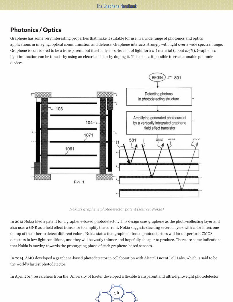
The Graphene Handbook
36
Photonics / OpticsGraphene has some very interesting properties that make it suitable for use in a wide range of photonics and optics
applications in imaging, optical communication and defense. Graphene interacts strongly with light over a wide spectral range.
Graphene is considered to be a transparent, but it actually absorbs a lot of light for a 2D material (about 2.3%). Graphene’s
light interaction can be tuned—by using an electric field or by doping it. This makes it possible to create tunable photonic
devices.
Nokia’s graphene photodetector patent (source: Nokia)
In 2012 Nokia filed a patent for a graphene-based photodetector. This design uses graphene as the photo-collecting layer and
also uses a GNR as a field effect transistor to amplify the current. Nokia suggests stacking several layers with color filters one
on top of the other to detect different colors. Nokia states that graphene-based photodetectors will far outperform CMOS
detectors in low light conditions, and they will be vastly thinner and hopefully cheaper to produce. There are some indications
that Nokia is moving towards the prototyping phase of such graphene-based sensors.
In 2014, AMO developed a graphene-based photodetector in collaboration with Alcatel Lucent Bell Labs, which is said to be
the world’s fastest photodetector.
In April 2013 researchers from the University of Exeter developed a flexible transparent and ultra-lightweight photodetector

The Graphene Handbook
37
made from graphene and graphExeter (a room-temperature transparent conductor discovered at the University of Exeter in
2012). This metal-free detector is only a few atoms thick and can be woven into textiles.
In China, researchers from Nanyang Technological University developed a new camera sensor made from graphene that can
detect a broad light spectrum, from visible to mid-infrared, at high sensitivity. The new sensor is 1,000 times more sensitive to
light than current imaging sensors, yet it uses 10 times less energy, as it operates at low voltages.
In 2010 UK and France-based researchers developed an ultra-fast mode-locked graphene-based laser. The teams continued
the research, and in 2013 they produced an enhanced laser device that produces a broad spectrum of infrared wavelengths.
They state that their results suggest it will be possible to create graphene-based lasers that emit light over the entire spectrum
of visible light.
In 2011 the first graphene-based optical switch (or modulator) was developed. Such devices form the basis of optical network
modulators (These use light to transmit data). The graphene modulator is the smallest and fastest modulator ever made.
The switching effect is enabled by the fact that graphene is transparent or opaque depending on the applied voltage, so you
can basically turn it off and on like a light switch. In 2013 UK researchers developed an enhanced few-layer graphene optical
switch that is nearly a hundred times faster than current switches. (The response rate is a few picoseconds.) This will hopefully
lead to faster telecommunication networks and may also have applications in security and medicine.
Medicine and biologyDue to graphene’s properties and unique mechanical features, some scientists are interested in how it can be used for
medicinal applications.
For example, graphene can be useful in fighting bacteria. Several studies in past years have demonstrated how graphene
can kill bacteria using several mechanisms—one of them being the simple fact that graphene can slice bacteria like a knife.
Graphene is also useful for photothermal antibacterial therapy and can be used to build a bacteria sensor.
Graphene may also be used for other applications in medicine and biology—artificial muscles, drug delivery, sensors, neural
stem cell research and production, dental prostheses, neural prostheses, cholesterol removal, MRI agents and more. Another
promising application for graphene is fast DNA sequencing, which was discussed in the membrane applications section above.
In September 2013 Grafoid and ProScan Rx Pharma announced a new joint-venture partnership to develop a graphene-based
nanotechnology platform for the precise targeting and thermal eradication of solid cancer tumors. This new platform aims
to overcome the side effects and strong limitations of common cancer therapies. The two companies have established a new
company called Calevia, to hopefully bring this new treatment to market.
LubricantsGraphene’s mechanical properties enable it to become a very good additive to lubricants. Recent research at the Argonne
National Laboratory demonstrated that graphene is an excellent steel lubricant—it dramatically reduces the amount of wear
and friction in sliding steel surfaces. The graphene lubricant also prevents oxidation of the steel surfaces when present at
sliding contact interfaces. The new lubricant also lasts longer than current lubricants.
In 2012 Angstron Materials developed a new graphene-modified lubricant, made by dispersing nanographene platelets (GNPs)
in a fluid containing a petroleum or synthetic oil. Angstron has demonstrated the ability of the new lubricant to provide
The Graphene Handbook
38
improved thermal conductivity and friction reduction.
Graphene NanoChem, a public company trading in the UK, is developing graphene-based lubricants for the oil and gas sectors.
The company’s PlatDrill fluid is in mass production, and NanoChem already signed an offtake agreement for 135,000 tonnes
over the next five years with Scomi Oiltools.
SpintronicsSpintronics technology uses electron spin in addition to its charge to build devices such as memory cells or computer chips.
Although spintronics is still in its early stages, some say it will replace electronics in the future, as spintronics chips will be
faster and much more energy efficient compared to electronics chips.
Graphene is a promising material for spintronics applications, and a lot of universities around the world are attempting to use
and modify the material to make is suitable for spintronics.
In 2014, researchers from MIT discovered that under a powerful magnetic field and at very low temperatures, graphene
can filter electrons according to the direction of their spin. By varying the magnetic field, you can switch the direction of the
electron movement - and perhaps create transistors and circuits.
In 2013 researchers from Spain succeeded in giving graphene magnetic properties—they basically managed to create a hybrid
graphene surface that behaves like a magnet (meaning that most electrons have the same spin).
A month after the Spanish research was published, researchers from the University of Manchester reported that they managed
to create elementary magnetic moments in graphene and then switch them on and off. This is the first time magnetism itself
has been toggled, rather than the magnetization direction being reversed—and it represents a major breakthrough on the way
toward graphene-based spintronics transistor-like devices.
In 2011 the National Science Foundation (NSF) granted a four-year $1.85 million research project to UC Riverside researchers
to develop a spin-based memory and logic chip. The researchers are working toward a graphene-based magneto-logic gate that
will serve as the engine for the new technology—similar to the role of the transistor in conventional electronics.
As was discussed before, graphene nanoribbons (GNRs) with zigzag type edges are spin polarized—which means they may be
useful for spintronics applications. For example, it is possible to produce spin valves based on zigzag GNRs.

The Graphene Handbook
39
Graphene materials marketWhile graphene technology is still in its infancy, several companies are already offering graphene and graphene-based
materials. Graphene sheets aren’t mass produced yet, but graphene flakes is a different story – several companies have
production plants that can produce tonnes of graphene flakes a year. And while a lot of the production is still used in research
and development products, some commercial production is already underhand.
The graphene market (at the material level) is still small – estimates range between $20 million and $40 million in 2014,
and forecasts range from about $100 to $250 million in 2020 and $150 to $400 million in 2024. Even though graphene is
exciting and the material may revolutionize entire industries, the market for materials will probably remain a small one in
the near future. Remember that production costs are estimated to drop sharply, so a tenfold growth in the next five years still
represents a huge increase in production capacity.
The current graphene (GNFs, mostly) production capacity is estimated at around 500 tons per year. The largest production
plants are probably Perpetuus Carbon’s 100-ton facility in the UK and XG Science’s xGnP 80-ton facility in Michigan. As
we said, production capacity is expected to increase sharply in the next few years, and many companies already announced
expansion plans. One of the largest planned fabs is Ningo Morsh’s 300-ton facility in China. It is yet to be seen whether this
plan will actually materialize.
The following sections will provide an overview of what’s available today and will also list products available from major
suppliers. Most of the companies mentioned have an online store, which makes sample purchases easy. All the sample
prices mentioned in this book were obtained via online store quotes at the time of writing. Please do not regard this as a
recommendation for the chosen companies or their products—because it isn’t. If you’re seeking help with finding the right
graphene partner, you may contact Graphene-Info as this is one of the services we offer.
It is important to note that material properties (such as uniformity, transparency, electron mobility and others) may differ
from company to company, as not all graphene materials are created equal. In fact one of the key problems with the graphene
market is the lack of standardization and accepted terminology, which is very confusing for anyone who wishes to adopt
graphene in their process, materials or products
Graphene sheets (large area graphene)Graphene sheets, made using CVD (usually) on several substrates, are currently very expensive. Even a small sized graphene
sheet (say 10x10 mm) may cost hundreds of dollars. Obviously this isn’t used for any products currently, but several
companies are offering such sheets for research and development purposes.
GrapheneaGraphenea is a private company based in Spain that is focused on the production of high quality graphene for industrial
applications. Graphenea currently offers monolayer, bilayer and trilayer graphene sheets on several substrates (Silicon, SiO2,
copper, quartz, PET and TEM grids).

The Graphene Handbook
40
Monolayer graphene on copper foil, 60x40 mm (source: Graphenea)
Graphenea also offers a “monolayer graphene on your substrate” service. You simply send your substrate to the company in
Spain and they will produce the graphene, transfer it to your substrate and ship it to you.
Sample products and prices:
À $59 for a pack of four 12mm circular monolayer graphene sheets on Copper
À $179 for a 10x10 mm graphene sheet deposited on your substrate
À $229 for a pack of four 10x10 mm monolayer graphene sheets on SiO2/Si
À $299 for a 60x40 mm monolayer graphene on Copper
À $399 for a 4” circular monolayer graphene on Copper
À $606 for a 10x10 mm bi-layer graphene sheet on SiO2/Si
À $849 for a 4” circular monolayer graphene wafer on SiO2/Si
À $857 fro a 10x10 mm tri-layer graphene sheet on SiO2/Si
Graphene LabsUS-based Graphene Laboratories develops and markets functional graphene materials and devices as well as other 2D
materials. Graphene Labs produces graphene sheets using a CVD process. The company operates two online stores—Graphene
Supermarket and Maximum Materials.
Graphene Labs offers graphene sheets on metals foils (nickel or copper) or on silicon (or SiO2). If you want graphene on your
own substrate, you can order graphene transfer tapes, or you can have the company transfer the graphene sheet to your own
substrate.
Sample products and prices:
À $100 for a pack of ten 10x10 mm multilayer graphene films on Nickel
À $195 for a pack of ten 10x10 mm single or double layer graphene sheets on 90 nm SiO2
À $200 for a 2x2” multilayer graphene sheet on Nickel

The Graphene Handbook
41
À $250 for a 2x2” monolayer graphene sheet on Copper
À $450 for a 4” circular monolayer graphene sheet on Copper
À $450 for a pack of ten 10x10 mm multi-layer graphene on 285 nm silicon (p-doped)
À $850 for a 4x4” monolayer graphene sheet on Copper
Graphene PlatformGraphene Platform was established in 2012 as a spin-off from Japan-based iTRIX to handle overseas sales. The company
offers large-scale graphene production and currently has two 4” thermal CVD systems and one 6” thermal CVD system.
Five pieces of 10x10 mm multi-layer graphene on SiO2
(source: Graphene Platform)
Graphene Platform offers CVD-grown graphene on copper foil (single layer) and on nickel foil (multilayer). The company also
offers single or multilayer graphene on PET, quartz glass and SiO2.
Sample products and prices:
À $150 for a 10x60 mm single-layer graphene sheet on Copper
À $150 for a 1x1” single-layer graphene sheet on quartz glass
À $175 for a 20x60 mm multi-layer graphene film on Nickel
À $250 for a pack of five 10x10 mm multi-layer graphene films on SiO2 (p-doped)
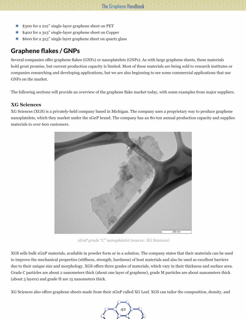
The Graphene Handbook
42
À $300 for a 2x2” single-layer graphene sheet on PET
À $400 for a 3x3” single-layer graphene sheet on Copper
À $600 for a 3x3” single layer graphene sheet on quartz glass
Graphene flakes / GNPsSeveral companies offer graphene flakes (GNFs) or nanoplatelets (GNPs). As with large graphene sheets, these materials
hold great promise, but current production capacity is limited. Most of these materials are being sold to research institutes or
companies researching and developing applications, but we are also beginning to see some commercial applications that use
GNFs on the market.
The following sections will provide an overview of the graphene flake market today, with some examples from major suppliers.
XG SciencesXG Sciences (XGS) is a privately-held company based in Michigan. The company uses a proprietary way to produce graphene
nanoplatelets, which they market under the xGnP brand. The company has an 80-ton annual production capacity and supplies
materials to over 600 customers.
xGnP grade “C” nanoplatelet (source: XG Sciences)
XGS sells bulk xGnP materials, available in powder form or in a solution. The company states that their materials can be used
to improve the mechanical properties (stiffness, strength, hardness) of host materials and also be used as excellent barriers
due to their unique size and morphology. XGS offers three grades of materials, which vary in their thickness and surface area.
Grade C particles are about 2 nanometers thick (about one layer of graphene), grade M particles are about nanometers thick
(about 3 layers) and grade H are 15 nanometers thick.
XG Sciences also offers graphene sheets made from their xGnP called XG Leaf. XGS can tailor the composition, density, and

The Graphene Handbook
43
manufacturing process to customize the sheet’s electrical, thermal and mechanical (thickness) properties.
Angstron MaterialsAngstron Materials is a privately held company based in Ohio. The company develops and manufactures GNPs and other
graphene-related products (such as single layer graphene sheets).
N008-N pristine graphene flakes powder (source: Angstron Materials)
Angstron Materials offers GNP powders in thicknesses ranging from 10 to 100 nm. The company has an online store with
prices available for small volume purchases.
Angstron’s 10–20 nm powder, for example, features approximate x-y dimensions of 14 um and a carbon content of about
97% (and an oxygen content of about 1.5%), and is being sold for $4 for one gram or $120 for 100 grams. Angstron states that
this powder is suitable for barriers, conductive and nanocomposites, heat radiation, conductive inks, conductive rubber and
conductive adhesive applications.
Another example is the company’s N008-N powder, which contains flakes that are 50–100 nm thick with x-y dimensions
of at most 5 um. The carbon content is 98% (and about 0.8% oxygen). This material costs $4 for one gram and $75 for 100
grams. It is said to be suitable for conductive and nanocomposites, heat radiation, conductive inks and conductive adhesive
applications.

The Graphene Handbook
44
Directa PlusDirecta Plus, established in 2005 in Italy, is a developer of innovative carbon nanomaterials, which include super-expanded
graphite, pristine GNPs, water-dispersed GNPs and fine nanographite powder (all of them marketed under the G+ brand).
Directa Plus has a 30-ton production facility in Como, Italy.
Directa Plus ZAPP G+ GNPs in polyolefin (70% wt)
Directa offers water-based dispersions of GNPs (up to 30%wt), pure nanopowders of GNPs (around 60 g/L), master batches of
GNP in polyolefin (70% wt) and highly concentrated (up to 35% wt) water-based pastes of GNPs without surfactant.
Graphene oxideGraphite oxide (GO) is a compound of graphite (carbon), hydrogen and oxygen. In GO the carbon layers (graphene sheets) are
separated by oxygen molecules. Graphite oxide can be reduced to graphene sheets (which are called reduced graphene oxide,
or r-GO). Most r-GO sheets contain many chemical and structural defects, but they have some interesting properties. For
example, by treating it with heat, light or chemicals, it can turn into a good conductor, which makes it suitable for transparent
conductive films. r-GO is also used to make composite paper-like materials and energy-related materials.
Many companies offer GO and r-GO materials. Bluestone Global Technology, for example, offers their Grat-GO products,
which are high-quality single-layer graphene oxide flakes dispersed in aqueous solutions. The flake size is between 1–20 um
and cost about $100 per 1000 mL (in concentration of 0.1mg/mL).
Graphene Labs offers graphene oxide as films, powders (flakes) or solutions. A round GO paper 4 cm in diameter that is not
conductive is on sale for $300. A 100-gram graphene graphene oxide powder costs $125. A highly-concentrated (6.2 g/L)
single-layer graphene oxide flakes solution costs $600 (for a 500 ml bottle that contains 3.1 GO grams).
Graphenea offers one gram of reduced graphene oxide powder for $169 (density of 1.91 g/cm3) and a 1000 mL water-
dispersed graphene oxide (4 mg/mL) for $395.

The Graphene Handbook
45
Graphene ribbonsGraphene nanoribbons (GNRs) are thin strips of graphene that can be metals, semiconductors, halfmetals, feromomagnets
and antiferomagnets—depending on the width, shape, edge structures and chemical termination. GNRs have an energy gap
and so have interesting applications in electronics.
As far as we know no one supplies these materials commercially today. At least two companies (Bluestone Global Tech and
Graphene Frontiers) are offering Graphene-FET (G-FET) products and these are based on GNRs. G-FET products will be
discussed below.
Graphene inksGraphene-based conductive inks are promising for many applications—such as RFID tags, heating elements (in car
windshields, for example), biosensors, computer keyboards and touch screens.
Graphene conductive ink (source: Vorbeck Materials)
There are several companies that already produce and sell graphene inks. The first company to commercialize graphene inks
was Vorbeck Materials, with their Vor-ink family of conductive inks that started shipping in 2012. Vorbeck offers inks suited
for gravure printing (VOR-INK Gravure), screen printing (VOR-INK Screen) and flexographic printing (VOR-INK Flexo). You
can buy samples online, and 500 grams of Vor-ink costs $100. (It’s the same price for the VOR Ink Gravure, Screen or Flexo.)
The second company to offer graphene inks was UK’s Haydale (a subsidiary of the ICL Group) that on June 2013 announced
the availability of their HDPlas Graphene Ink Sc213. Those inks have been optimized for ideal viscosity and solid contents,
ensuring excellent coverage and exceptional conductivity. The 100 gram research sample costs £200 ($310 USD) or £2,000/
kg, while the 5 kg sample costs £2,225 ($3,430) or £445/kg. The price for commercial quantities is considerably lower, to
under $200/kg. Haydale can produce over 20 tons of graphene ink per year.
In March 2014 UK’s Perpetuus Carbon Technologies launched a graphene-based ink developed in collaboration with the
Gwent Electronics Group. The ink features a resistance below one ohm per square centimeter (Perpetuus claims this is the
most conductive graphene-based ink in the world). Perpetuus’ inks are available in formulations for ink jet, flexographic
printing and sensors technologies.

The Graphene Handbook
46
Graphene compositesGraphene composite (or hybrid) materials represent a promising solution to many applications. It is possible to add graphene
to metals, polymers or ceramic—and make them stronger, more conductive and more heat resistant.
Recently, for example, Graphenea discovered that adding graphene to ceramic alumina can make it stronger—it is up to
50% less likely to break under strain. Other mechanical properties stayed on par with untouched alumina, while electrical
conductivity increased by a factor of a hundred million.
Composite materials are used in most graphene-enhanced products on the market today, and it seems that for the near future
this will be the most popular graphene application. Dozens of graphene-flake producers offer composite material development
services and material supply options.
One popular matrix for graphene composites is carbon-fibers. Several companies offer such materials, and several products
are on the market – for example in 2014 Vittoria launched the world’s “faster bicycle wheels” – made from carbon-fiber
graphene composites (supplied and developed by Directa Plus).
UK’s Haydale, for example, is developing graphene-enhanced composites. In November 2014, Haydale acquired EPL
Composite Solutions, to boost the company’s composite offerings. Haydale has shown that carbon-fiber and graphene
composites are stronger and resist damage better than carbon-fiber materials. In October 2014, the U.S based Angstron
Materials started to offer graphene-enhanced polymers with superior mechanical, electrical and thermal properties.
Graphene FETs (GFETs)In October 2013 Bluestone Global Tech started shipping the world’s first graphene field-effect transistor (GFET). BGT
produces Grat-FET graphene wafers, with nine different GFET arrays (or chips), each with 36 individual FETs.
Grat-FET channel scheme (source: Bluestone Global Tech)
BGT’s GFETs are fabricated (using CVD) on a silicon wafer covered with a SiO2 layer. The high mobility (2000 cm2/Vs
or more) graphene is used as the transistor channel. Each transistor consists of three terminals: source and drain metal
electrodes and a global back gate.

The Graphene Handbook
47
GFETs are basic building blocks for devices, and will hopefully find their way into applications such as gas or chemical sensors,
photodetectors and graphene electronic circuits. BGT’s GFETs are still very expensive, but BGT claims they are ready for
mass production. Obviously prices will need to drop drastically before we’ll see these devices in a commercial product. BGT
currently sells these chips to both academic and industrial customers. The readily accessible standard GFETs can save a lot of
time and effort.
Graphene Frontiers’ Six-Sensors G-FET sensors
In July 2014, US-based Graphene Frontiers launched the “six sensors” brand for highly-sensitive chemical and biological
GFET-based sensors that can be used to diagnose diseases with multiple markers such as cancer and illnesses currently
diagnosed using ELISA technologies. The sensor is based on a functionalized graphene field effect transistor (GFET). The
unique properties of graphene enable detection of molecules in femtomolar (fM) concentrations - this is vastly better than any
other sensor on the market. Graphene Frontiers will first enter the research-use-only (RUO) market with a basic, customizable
product. This is a limited volume market (orders may reach a few hundreds of chips), but later on they want to also enter the
diagnostic and consumer health markets - which may require tens of millions of chips.
Graphene Frontiers’ Six-Sensors G-FET sensor schema
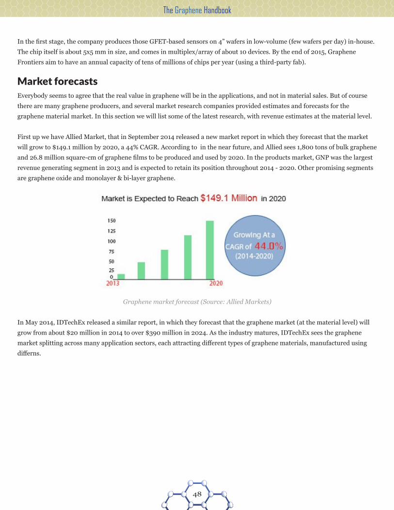
The Graphene Handbook
48
In the first stage, the company produces those GFET-based sensors on 4” wafers in low-volume (few wafers per day) in-house.
The chip itself is about 5x5 mm in size, and comes in multiplex/array of about 10 devices. By the end of 2015, Graphene
Frontiers aim to have an annual capacity of tens of millions of chips per year (using a third-party fab).
Market forecasts Everybody seems to agree that the real value in graphene will be in the applications, and not in material sales. But of course
there are many graphene producers, and several market research companies provided estimates and forecasts for the
graphene material market. In this section we will list some of the latest research, with revenue estimates at the material level.
First up we have Allied Market, that in September 2014 released a new market report in which they forecast that the market
will grow to $149.1 million by 2020, a 44% CAGR. According to in the near future, and Allied sees 1,800 tons of bulk graphene
and 26.8 million square-cm of graphene films to be produced and used by 2020. In the products market, GNP was the largest
revenue generating segment in 2013 and is expected to retain its position throughout 2014 - 2020. Other promising segments
are graphene oxide and monolayer & bi-layer graphene.
Graphene market forecast (Source: Allied Markets)
In May 2014, IDTechEx released a similar report, in which they forecast that the graphene market (at the material level) will
grow from about $20 million in 2014 to over $390 million in 2024. As the industry matures, IDTechEx sees the graphene
market splitting across many application sectors, each attracting different types of graphene materials, manufactured using
differns.

The Graphene Handbook
49
Graphene market forecast (Source: IDTechEx)
Earlier in 2014, Yole Development released their own forecast, in which they see a $141 million graphene material market in
2024, driven mainly by transparent conductive electrodes and energy storage applications. According to Yole, the market in
2013 was about $11 million, and it will grow slowly till 2017. In 2019 the market will experience faster growth (35.7% CAGR).
Graphene market forecast (Source: Yole Developpement)
In September 2013, BCC Research released the most optimistic report yet – they forecast that the global graphene product
market will reach $195 million in 2018, and will grow quickly to $1.3 billion by 2023 (an annual compound annual growth rate
of 47.1%).

The Graphene Handbook
50
Products with graphene on the marketWhile there are dozens of companies developing graphene applications or supplying graphene-based materials, very few devic-
es or products that use graphene-based materials are actually on the market.
As far as we know, MWV Packaging’s Siren Technology (introduced in early 2012) was the first product to use graphene. The
Siren is security tags (labels) that use Vorbeck Materials’ graphene-based inks. The labels are cheap (a few cents per label) and
are made using a flexographic roll-to-roll printing process. The labels are to be connected with a reusable electronic module
that can sound an alarm via an integrated speaker.
In the beginning of 2013, HEAD announced their new range of graphene tennis rackets (YouTek Graphene Speed series).
These rackets supposedly use graphene to make the shaft stronger and lighter, and HEAD states that the graphene helps dis-
tribute the weight better and creates a stronger and better controlled racket. HEAD offers five different rackets, ranging from
$170 to $286. It’s not clear what material HEAD uses exactly in this product and who the graphene supplier is, but it is likely
to be graphene flakes provided by Applied Graphene Materials.
HEAD YouTek Graphene Speed racket
In 2014, several more sport-equipment products that use graphene appeared on the market. HEAD launched a line of gra-
phene-enhanced skis for women, called Joy, which are meant to be lightweight and durable.
A Spanish company called Catlike launched a line of cycling helmets called Mixino 2014, enhanced with graphene. These hel-
mets are said to be light and strong, and offer major improvements in the field of safety and impact absorption. The company
also offers a line of graphene-enhanced cycling shoes to hit the market in early 2015. The line is called whisper and combines
different kinds of cycling shoes (for road, mountain and triathlon biking). The shoes are supposed to provide superior perfor-
mance by being light and durable.

The Graphene Handbook
51
Catlike Mixino 2014 graphene-enhanced helmet
In October 2014, Vittoria released a new range of bicycle race wheels that are built from graphene-enhanced composite mate-
rials. The new wheels (called Qurano) are the best wheels offered by Vittoria, and they say these are the fastest wheels in the
world - all thanks to graphene. Vittoria uses graphene materials produced by Italy’s Directa Plus, added to their carbon-fiber
matrix built wheel rim.
In June 2013 China’s Powerbooster Technology claimed that they had developed graphene-based flexible touch-panels for
mobile devices. The company states they are already producing those panels—in fact they are making around 2 million panels
per month. Those numbers aren’t confirmed yet, but we do know that those panels use graphene supplied by Bluestone Global
Tech and China’s Ningo Morsh.
The Graphene Handbook
52
Investing in grapheneGraphene may have a very bright future and might revolutionize entire industries—and so many investors are seeking possible
ways to benefit from this upcoming revolution.
Investing in graphene is not easy, though. Most pure-play graphene companies are still at an early stage, generating very little
(if any) revenues and represent a high risk investment. It is very difficult to estimate at this stage which companies will emerge
as leaders in this field. In the coming sections we’ll detail some possible ways to invest in graphene.
Pure play graphene companiesThere are several pure-play graphene public companies, most of them based in the UK, trading in the AIM stock exchange.
Haydale (AIM:HAYD) develops and markets carbon materials under the HDPlas brand. The company currently focuses on
graphene, CNTs and zinc nanomaterials, and also developed metal-free graphene-based inks. In October 2013 we posted an
article explaining Haydale’s business and technology.
Applied Graphene Materials (previously Durham Graphene Science) was established in 2010 as a spin-off from Durham
University to develop a new graphene synthesis method and produce graphene materials. AGM’s technology is a unique
patented scalable ‘bottom-up’ CVD approach to produce graphene. In 2013 the company announced plans to go public and list
on the UK’s AIM stock exchange.
Carbon Sciences is developing a graphene production process technology that was originally invented at the University of
California, Santa Barbara (UCSB). The process transforms natural gas into commercial size sheets of graphene that can be
fine-tuned with application-specific electrical and materials properties. Carbon Sciences is a public company trading on the
NASDAQ (OTC:CABN).
Cientifica (AIM:CTFA) started trading in October 2013 when they raised only £241,000 ($389,000) to invest and acquire
graphene application businesses. They have an option to acquire 49.9% in RainMaker and are also collaborating with London
Graphene. In 2014 the company wanted to raise more funds but failed. With so little funds, investment seems highly risky, and
trading in the company’s shares stopped towards the end of 2014.
Graphene 3D Lab (TSX:GGG) is focusing on development of high-performance graphene-enhanced materials for 3D
printing. The company was spun-off Graphene Labs with support from Lomiko Metals (who holds 15% of the company). In
August 2014 graphene 3D Lab went public after a reverse merger with Matnic Resources.
Large public companiesSeveral large and public companies, including Samsung, Intel, Nokia, IBM and Sony, are involved with graphene R&D. While
the research at those companies is very advanced (Samsung holds the largest number of graphene patents in the world, for
example), graphene represents a small portion of their business. Even if graphene fulfills its promise, it’s not likely to change
those companies’ business and revenues in a major way.
The Graphene Handbook
53
Manufacturing equipment makersInvesting in the companies that supply manufacturing equipment and related tools may be a good way to enjoy the future
graphene boom (if it happens). Remember, though, that graphene-producing equipment usually represents just one segment
of these companies’ business.
Aixtron AG is a provider of deposition equipment to the semiconductor industry, and the company offers the BM Pro
systems (previously called Black Magic systems). These systems are used to deposit graphene (and CNTs) using both chemical
vapor deposition (CVD) and plasma enhanced chemical vapor deposition (PECVD). Aixtron trades in the NASDAQ (ticker:
AIXG).
CVD Equipment Corporation (a US-based company) offers a variety of process and support equipment for both R&D and
production facilities. CVD offers graphene materials and other services for graphene production and processing. The company
is also co-developing graphene-based lithium battery electrodes with Norway’s Graphene Batteries. CVD Equipment trades in
the NASDAQ (ticker: CVV).
Graphite mining companiesGraphite (stacked graphene sheets) is used today in many applications and is already a big market. There are several graphite
miners that are trying to enter the graphene market via investments or cooperations, and some of these companies are public.
Note, however, that these companies usually simply want to help create a new market for graphite, and their financials will
mostly be tied to the mining operations and not graphene itself.
Focus Graphite (based in Canada) is a mid-tier junior graphite mine developer and technology developer company. Focus
Graphite owns the highest-grade (roughly 16%) technology graphite resource in the world (at Lac Knife in Quebec). The
company owns 40% of Graphene startup Grafoid (these two companies are also collaborating on R&D). Focus Graphite
trades in the Canadian market and in the OTC market (ticker: FCSMF).
Bora Bora Resources (based in Australia) is a graphite exploration company with a suite of high grade graphite projects in
Sri Lanka. In June 2014 Bora Bora Resources signed into a binding heads of agreement with Sri Lanka’s RS Mines (a graphite
miner that also produces graphite oxide (GO). BBR is also collaborating with Monash University on a graphene project. BBR is
a public company, trading in the Australian Securities Exchange (ASX: BBR).
Mason Graphite (based in Canada) is a Canadian mining company focused on the exploration and development of its 100%
owned Lac Gueret graphite project in northeastern Quebec. In January 2014, Mason Graphite acquired 40% of graphene R&D
company NanoXplore. Mason Graphite trades in the Toronto stock exchange (ticker: LLG).
Northern Graphite Corporation is a Canadian mine development company, and its main asset is the Bissett Creek
graphite project located 100km east of North Bay, Ontario. The company is also involved with Graphene research. NGC trades
in the Canadian stock exchange (ticker: NGC) and in the OTC (ticker: NGPHF).
National Graphene Corporation a US company that is focused on bringing the Chedic Graphite Mine back into
commercial production. In June 2013 they signed an agreement with American Graphene to jointly explore graphene

The Graphene Handbook
54
opportunities and employ a new sonication process to reduce graphite to graphene. The company is public and trades in the
OTC (OTCQB: NGRC).
Lomiko Metals an exploration-stage Canadian company that aims to acquire and develop mineral resources in Canada.
It primarily explores graphite, zinc and gold. Lomiko owns several resource properties containing high-grade graphite, and
the company has signed a strategic alliance with Graphene Labs to co-develop a vertically integrated graphene supply chain.
Lomiko holds 15% in public Graphene 3D Labs, has a stake in newly formed graphene supercapacitor developer Graphene
ESD, and has also an internal graphene R&D department. Lomiko Metals is a public company, trading in the TSX (ticker:
LMR.V).
GrafTech International is a global company with more than 120 years of experience in the carbon and graphite industry.
GrafTech makes an expanded natural graphite foil that keeps most of graphene’s properties (thermal, electrical, and possibly
acoustic). The company says that their graphite-foil is used in many devices, including the iPhone and Samsung’s new TVs.
The company is public and trades in the NYSE (ticker: GTI).
American Graphite Technologies (AGT) is a mineral exploration and technology development company. AGT has 100%
ownership of 100 mineral claims in Quebec, Canada (close by to Focus Graphite’s proven graphite resource). AGT is also
involved with graphene related technologies and is partnering with CTI Nanotechnologies LLC. AGT is trading in the
NASDAQ (OTCBB: AGIN).
Australia-based Talga Resources holds a high-grade graphite mine in Sweden (in addition to gold and iron mines in
Australia). The company is also producing graphene on a very small scale, but may become a full-scale graphene producer (in
a Sweden-based plant).
Our final graphite company is Carbon Graphite Group, based in Chengguan Town (Xinghe). CCG manufactures and sells
graphite-based products in China. CCG’s products include graphite electrodes, fine grain graphite blocks and high purity
graphite. CCG is also active with graphene technology research. CCG is trading in the NASDAQ’s OTC market (ticker: CHGI).
Indirectly investingAnother possibility to invest in graphene is to buy shares in a public company that owns or holds a stake in a private graphene
company. One such possibility is POSCO, a public company (NYSE: PKX) that holds 20% of XG Sciences.
As was mentioned before, Focus Graphite owns 40% of graphene developer Grafoid, and it trades in the OTC market
(ticker: FCSMF).
More optionsGraphene Nanochem is a UK based company that holds the exclusive license to a process known as Catalyx which
uses a catalyst to extract graphene from biogases (such as methane). This process can potentially mean low-cost graphene
production. They are also offering graphene-enhanced lubricants for use in the extraction of shale gas, and signed an off-take
agreement for their entire production capacity (135,000 ton) in the near future. Graphene Nanochem is trading in the UK’s
AIM (ticker:GRPH).
The Graphene Handbook
55
Valence Industries is an Australian industrial manufacturing company that produces high grade flake graphite products. In
March 2014 Valence launched the Graphene Research Centre in collaboration with the University of Adelaide, with hopes to
start initial graphene product sales in the first half of 2014. Valence is a public company that trades in Australia (ASX:VXL).
Strategic Energy Resources (SER) is an Australian based explorer with a diversified portfolio of mineral assets. In May
2014 the company announced it is resolved to focus on graphene related investments. The company holds a stake in Valence Industries, also involved with graphene (see above). SER is a public company, trading in the Australian Stock Exchange
(ASX:SER).
As of the time of writing, the author of this book does not hold shares in any of the above mentioned companies.

The Graphene Handbook
56
Large graphene projectsIn the past few years, several governments and large corporations announced some very exciting graphene research and devel-
opment projects. Here’s a list of some of the most prominent ones.
The Graphene FlagshipIn January 2013, Europe selected the Graphene Flagship project as its first $1billion 10-year research program. The project
was officially launched in October 2013. The project is led by theoretical physicist Jari Kinaret at Sweden’s Chalmers Univer-
sity.
The project’s charter is to focus on developing graphene applications in the computing, batteries and sensor markets. The
project started with 75 academic and industrial partners from 17 European countries, but during 2014 it grew to 141 partners
from 19 countries.
Graphene Flagship is currently in its ramp-up phase which will last till March 2016. This phase received funding of €54 mil-
lion. The steady-state phase (2016-2020) will receive funding of €50 million per year.
The UK’s graphene investmentsGraphene was first isolated and studied in The University of Manchester in the UK. This University is still one of the world’s
leaders in graphene research, and the UK is attempting to establish a graphene development hub (a Graphene Valley of sorts)
in the area. The UK government already committed £356 million (over $500 million) in the past few years towards that goal.
The first project was the £61 million National Graphene Institute (NGI), which was announced towards the end of 2011 and
its inauguration is scheduled for March 2015. Most of the money went into constructing the building itself and purchasing
research equipment. The UK government also allocated a large investment to support graphene engineering research and
graphene market development.
The second Manchester project, the Graphene Engineering Innovation Centre (GEIC), was announced in September 2014.
This center (which will receive a similar £60 million investment) will focus on development of graphene-based products with
an eye on commercialization. Half of the funding for the GEIC will come from Abu Dhabi investors Masdar.
In December 2014, the UK government announced the third initiative – a £235 million advanced materials research center,
called the Sir Henry Royce Institute for Advanced Materials Research and Innovation. The Center will be based in Manchester,
but will also have satellite branches in Leeds, Liverpool, London, Cambridge, Oxford and Sheffield. The charter of this center
will be to
investigate the rapidly growing field of materials (not just graphene) science across a range of disciplines including engineer-
ing, nanotechnology and chemistry.
IBM next-gen chip material driveIn July 2014, IBM announced an ambitious project to find the next-generation chip technology. It is getting more and more
difficult to shrink silicon chips and IBM says that Silicon is simply reaching its limit.

The Graphene Handbook
57
IBM will allocate $3 billion over the next five years ($600 million per year), allocated from its existing R&D budget, to look
into several alternatives - including graphene, carbon nanotubes, quantum computing and silicon photonics.
Korea’s $40 million graphene support fundIn May 2013, South Korea announced a plan to spend 47 billion Won (around $40 million) in the next six years to help local
companies commercialize graphene. More than half of the investments will be given to small businesses.
Korea ranks third in the world by number of graphene patents. Samsung is the company that holds the largest amount of
graphene patents in the world, while Korea’s Sungkyunkwan University is the world’s leading research institute ranked by the
number of graphene patents.

The Graphene Handbook
58
Main graphene challengesWhile graphene is exciting, there are many challenges ahead before this material can actually revolutionize industries and en-
able new applications. In the following sections, several major challenges are detailed, although many more exist.
Mass productionAs was discussed earlier in this book, mass production of graphene hasn’t really begun. Of course, when we talk about gra-
phene we actually discuss a class of materials, so let’s take a look at them all.
While some technologies and processes exist to create large-area single-layer graphene sheets, we’re still far away from actu-
ally producing such sheets in a commercial way, let alone true mass production. Currently this production is being done for
R&D only, and it is being done “by hand” using slow and expensive processes.
There are other graphene materials that are easier to make, such as graphene flakes (or nanoplatelets), graphene oxide or few-
layer graphene. While some companies are producing such materials already, usually these are just samples done in relatively
low volume. Just to show how low this volume really is, consider that XG Science, one of the market leaders in GNPs, can
produce 80 tons in a year. One of the applications for those materials is Li-Ion battery anodes. The global market for anode
materials alone is estimated at 50,000 tons per year!
So we’re still searching for the best way to mass produce graphene sheets and flakes—a process that may actually lead toward
real mass production. It may require a large investment to actually establish such a mass production fab and, of course, the
producer will have to find the right market for these materials to make the investment worthwhile.
CostSingle-layer, high quality graphene sheets are terribly expensive, and production volume is very limited. Bringing the cost
down is a major challenge and requires new production processes and probably large investments.
Graphene flakes and graphene oxide are a lot easier and cheaper to produce. Worldwide production capacity is estimated at
almost 1,000 tons per year and some companies claim that the cost issues have been resolved for these materials and they can
compete in the market.
HandlingActual handling of graphene sheets is a tricky business. Single layer graphene is very thin, and the material tends to re-stack
into graphite if it is left to itself (if there is more than one sheet nearby, of course). It is always difficult to handle and transfer
those sheets. Graphene is almost always produced on a substrate (such as silicon or copper), and then it can be transferred to
the final substrate—but doing so in a precise controlled way is still a challenge.
If we take a look at dry graphene powder (graphene flakes or sheets), these may pose a health hazard (like many other
nanoparticles) and should be handled with care. Most graphene flakes are sold in solvent.
The Graphene Handbook
59
StandardizationGraphene materials remain very confusing. There are still many naming conventions that need to be agreed upon—and this
keeps getting worse as more and more materials and processes are created and discovered.
For example, what is few-layer-graphene exactly, and how many layers will it take to turn it into 3D graphene, or graphite?
What exactly is a graphene flake or nanoplatelet? Will we have a standard for the shape, width, concentration, etc.?
Many companies say that their materials are of “high-quality.” But, of course, some processes result in better graphene, while
other processes will produce lower-quality graphene but at a lower cost, so it’s not clear how exactly to name these different
qualities’ attributes and how to enforce the naming conventions. In addition some graphene materials simply have different
properties – better at heat conduction, but less suited for electronic conduction, etc.
Bandgap enablingOne of the major challenges for graphene-based electronics is the fact that graphene does not have a bandgap, required to
make graphene a semiconductor. While there are many ways to introduce a bandgap (and even ways to enable logic circuits
without a bandgap), this is still a major challenge that many researchers are working on.
The Graphene Handbook
60
Appendices
Appendix A: Glossary
Atomic Force Microscopy (AFM): A microscope that uses a mechanical probe to touch a sample and gather information.
Bandgap: An energy range in which electrons cannot exist. Bandgap is required to enable electronic switching. Graphene in
its basic form doesn’t have a bandgap.
Buckyballs: Spherical fullerene molecules (C60). These cage-like structures (officially called Buckminsterfullerene) can bind
a large number of hydrogen atoms and may be useful in many applications in medicine, energy storage, energy generation and
more.
Carbon Nanotubes (CNT): Cylindrical-shaped carbon sheets (basically these are rolled-up graphene sheets) with great
thermal, mechanical and electrical properties.
Chemical Vapor Deposition (CVD): A production process that deposits a material in gas form on a substrate in a closed
chamber.
Fullerene: A spherical (or tube or ellipsoid) all-carbon molecule.
Graphane: A graphene sheet terminated with hydrogen atoms. Graphane is similar to graphene, but acts as an insulator.
Graphene Flakes (GNFs): Small pieces (flakes) of graphene. These are easier to make compared to large graphene sheets,
but they still retain many of graphene’s great attributes (these depend on the flake’s quality and shape).
Graphene Nanoplatelets (GNPs): A nanoplatelet is a small disk-shaped particle. In theory, graphene nanoplatelets are
disk-shaped graphene flakes. But in practice, most companies offering platelets are simply offering flakes, not necessarily in
disk shapes.
Graphene Nanoribbons (GNRs): Thin (under 50 nm usually) strips of graphene. Graphene nanoribbons have a bandgap,
and the width and edges of the ribbons change their electronic properties.
Graphene Oxide (GO): A compound of graphene, hydrogen and oxygen. GO is easy to make and is usually reduced to create
graphene sheets (called reduced-GO, those suffer from many chemical and structural defects).
ITO: Indium Tin Oxide, the current choice technology for transparent electrodes. ITO is expensive and brittle, and a suitable
replacement is continuously searched for.
Molecular Beam Epitaxy (MBE): A vacuum deposition technology that enables graphene synthesis at lower temperatures
compared to CVD.

The Graphene Handbook
61
Molybdenum Disulfide (MDS, MoS2): A material made from sheets of molybdenum atoms sandwiched between two
sulfur atoms. MDS may replace silicon to enable more efficient electronics and energy devices.
OLED: Organic Light Emitting Diode, an emerging emissive display and lighting technology.
Quantum Dot (QD): A tiny semiconductor with electronic properties somewhat between that of a bulk material and a dis-
crete molecule. It is possible to produce a quantum dot made from graphene.
r-GO: Reduced Graphene Oxide (see Graphene Oxide).
Raman Spectroscopy: A research tool that uses laser light to interact with molecular vibration or other excitations.
Scanning Electron Microscopy (SEM): A microscope that uses a focused beam of electrons, used to understand sample
topography and composition.
Spintronics: A technology that uses electron spin in addition to its charge to build memory or logic devices
Transmission Electron Microscopy (TEM): A microscope that uses an electron beam that passes through an ultra-thin
sample.

The Graphene Handbook
62
Appendix B: Other carbon allotropes
Allotropes are different structural modifications of an element, and carbon has several known allotropes beside graphene,
such as graphite, CNTs, diamond and fullerene. These materials share some properties with graphene, and here we present a
very short introduction to those common carbon allotropes. (There are dozens of possible carbon allotropes, but only a few are
discussed here.)
GraphiteGraphite is one of the most common carbon allotropes and has been in use for centuries (it was used in southeast Europe to
make ceramic paint as far back as the 4th millennium B.C.). First usages were indeed as a pigment, and even today most pencil
cores are made from graphite mixed with clay (the word graphite comes from the Greek word Graphein, which means to write
or to draw). Today about 1.1 million tons of graphite are mined around the world each year.
Graphite structure and a natural specimen
Graphite is a great electrical and thermal conductor, and under standard conditions it is the most stable form of carbon. (It is
stable even at very high temperatures in excess of 3,600 degrees Celsius.) It is a very strong and stiff natural material, and it
is highly resistant to chemicals and wear. It is also an excellent lubricant. Graphite applications today include battery anodes,
lubricants, brake lining, steelmaking, pencils and various specialized applications.
Graphite is made from stacked sheets of graphene. When graphene is “left to itself” it will quickly organize itself into graphite.
The first method to produce graphene sheets was to exfoliate them from graphite.
Carbon Nanotubes (CNTs)A carbon nanotube (usually referred to as CNT) is a cylindrical allotrope of carbon that looks like a rolled-up graphene sheet.
CNTs were first discovered about 50 years ago, but only in 1991 did the scientific community start to really research and
develop CNTs. Nanotubes are usually categorized as either single-walled (SWNTs) or multi-walled (MWNTs).

The Graphene Handbook
63
A Single-Walled Carbon Nanotube (SWCNT)
Like all carbon allotropes, CNTs have remarkable properties. CNTs are very strong and elastic and (depending on the
structure) can be either conducting or semiconducting. CNTs also offer interesting thermal and optical properties.
Like graphene, CNTs could theoretically be used for many applications due to their mechanical, thermal and electrical
properties. In practice, however, commercial usage is limited to “unorganized” mass CNT materials that aren’t as strong as
high quality CNT materials; as a result CNTs aren’t widely used today.
In May 2013 Bayer Material Science, one of the leaders in CNT production, decided to stop producing CNTs, saying that the
“potential areas of application that once seemed promising from a technical standpoint are currently either very fragmented or
have few overlaps with the company’s core products.” This led many to speculate that the CNT market will never take off (even
though Bayer itself says that CNTs have a “huge potential”).
One of the possible ways to create graphene nanoribbons (which are promising for electronics applications) is to open (or
unzip) a carbon nanotube.
DiamondsDiamonds are natural carbon allotropes in which the atoms are arranged in a special structure called a diamond lattice
(see image below). Diamonds in nature are impure and contain nitrogen and boron atoms—which create the clear colorless
appearance of a natural diamond.
Diamond structure and cut diamonds

The Graphene Handbook
64
Diamonds are very stable (although they are less stable than graphite). Due to the strong covalent bonding between the carbon
atoms, diamonds are very strong—and in fact they are the hardest and most thermal conductive 3D material known. Most
diamonds are excellent electrical insulators.
Diamonds are, of course, a valuable gemstone, but the material is also used in industry (due to the hardness and strength),
mostly for cutting (for example, cutting glass) and precision instruments. Diamonds contain a natural impurity (nitrogen-
vacancy center) that has a long-lived single-electron spin state, and so diamonds are promising for future Spintronics devices
and quantum computing.
Diamonds can also be synthesized using CVD or by applying a high pressure at high temperatures (i.e. simulate natural
diamond production). There are some materials such as cubic zirconia and silicon-carbide that resemble diamonds in
appearance and in some properties, and these are sometimes referred to as a diamond simulants.
Fullerene and buckyballsFullerene is a family of carbon allotropes shaped like a sphere, ellipsoid or tube. A carbon nanotube, for example, is a type of
fullerene. Spherical fullerenes are also called buckminsterfullerene or buckyballs, and these look like a graphene ball.
Fullerene structure (C60)
Buckyball was also the first synthesized fullerene molecule, back in 1985. Later on fullerenes were discovered in nature and
even in outer space. It turns out that fullerenes are very common in nature (for example, in candle-soot). In fact, fullerene is
the most common carbon allotrope after graphite and diamond.
Buckyballs (which look like soccer balls) can come in different sizes. The most common one (and the one first synthesized) is
the C60 (also called buckminsterfullerene). The smallest buckyball is C20.
Buckyballs are superconductors and are very strong. Fullerenes may be useful across many industries such as medicine,
energy storage, electronics, spintronics, optics and more.
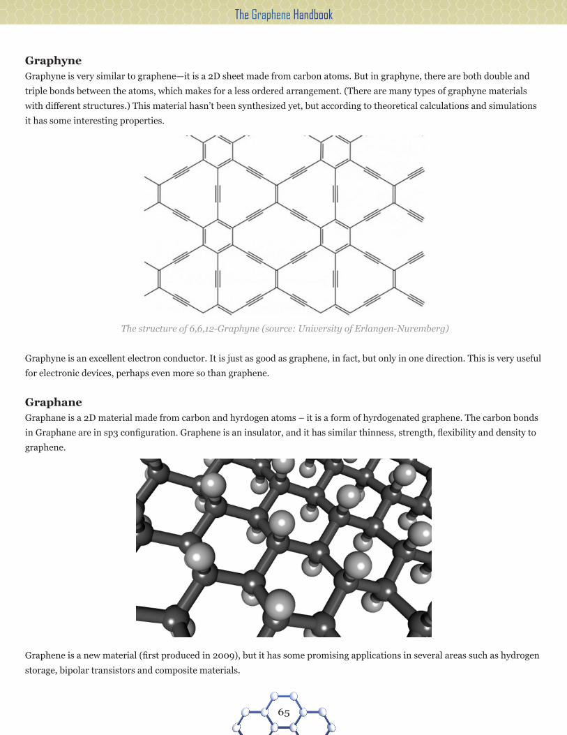
The Graphene Handbook
65
GraphyneGraphyne is very similar to graphene—it is a 2D sheet made from carbon atoms. But in graphyne, there are both double and
triple bonds between the atoms, which makes for a less ordered arrangement. (There are many types of graphyne materials
with different structures.) This material hasn’t been synthesized yet, but according to theoretical calculations and simulations
it has some interesting properties.
The structure of 6,6,12-Graphyne (source: University of Erlangen-Nuremberg)
Graphyne is an excellent electron conductor. It is just as good as graphene, in fact, but only in one direction. This is very useful
for electronic devices, perhaps even more so than graphene.
GraphaneGraphane is a 2D material made from carbon and hyrdogen atoms – it is a form of hyrdogenated graphene. The carbon bonds
in Graphane are in sp3 configuration. Graphene is an insulator, and it has similar thinness, strength, flexibility and density to
graphene.
Graphene is a new material (first produced in 2009), but it has some promising applications in several areas such as hydrogen
storage, bipolar transistors and composite materials.
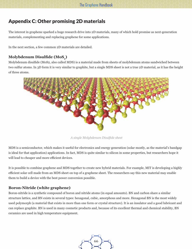
The Graphene Handbook
66
Appendix C: Other promising 2D materials
The interest in graphene sparked a huge research drive into 2D materials, many of which hold promise as next-generation
materials, complementing and replacing graphene for some applications.
In the next section, a few common 2D materials are detailed.
Molybdenum Disulfide (MoS2)Molybdenum disulfide (MoS2, also called MDS) is a material made from sheets of molybdenum atoms sandwiched between
two sulfur atoms. In 3D form it is very similar to graphite, but a single MDS sheet is not a true 2D material, as it has the height
of three atoms.
A single Molybdenum Disulfide sheet
MDS is a semiconductor, which makes it useful for electronics and energy generation (solar mostly, as the material’s bandgap
is ideal for that application) applications. In fact, MDS is quite similar to silicon in some properties, but researchers hope it
will lead to cheaper and more efficient devices.
It is possible to combine graphene and MDS together to create new hybrid materials. For example, MIT is developing a highly
efficient solar cell made from an MDS sheet on top of a graphene sheet. The researchers say this new material may enable
them to build a device with the best power conversion possible.
Boron-Nitride (white graphene)Boron-nitride is a synthetic compound of boron and nitride atoms (in equal amounts). BN and carbon share a similar
structure lattice, and BN exists in several types: hexagonal, cubic, amorphous and more. Hexagonal BN is the most widely
used polymorph (a material that exists in more than one form or crystal structure). It is an insulator and a good lubricant and
can replace graphite. BN is used in many cosmetic products and, because of its excellent thermal and chemical stability, BN
ceramics are used in high temperature equipment.
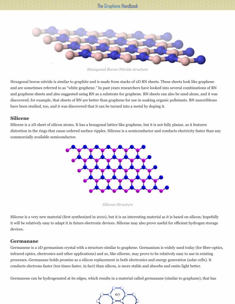
The Graphene Handbook
67
Hexagonal Boron-Nitride structure
Hexagonal boron-nitride is similar to graphite and is made from stacks of 2D BN sheets. These sheets look like graphene
and are sometimes referred to as “white graphene.” In past years researchers have looked into several combinations of BN
and graphene sheets and also suggested using BN as a substrate for graphene. BN sheets can also be used alone, and it was
discovered, for example, that sheets of BN are better than graphene for use in soaking organic pollutants. BN nanoribbons
have been studied, too, and it was discovered that it can be turned into a metal by doping it.
SiliceneSilicene is a 2D sheet of silicon atoms. It has a hexagonal lattice like graphene, but it is not fully planar, as it features
distortion in the rings that cause ordered surface ripples. Silicene is a semiconductor and conducts electricity faster than any
commercially available semiconductor.
Silicene Structure
Silicene is a very new material (first synthesized in 2010), but it is an interesting material as it is based on silicon; hopefully
it will be relatively easy to adapt it in future electronic devices. Silicene may also prove useful for efficient hydrogen storage
devices.
Germanane Germanene is a 2D germanium crystal with a structure similar to graphene. Germanium is widely used today (for fiber-optics,
infrared optics, electronics and other applications) and so, like silicene, may prove to be relatively easy to use in existing
processes. Germanane holds promise as a silicon replacement in both electronics and energy generation (solar cells). It
conducts electrons faster (ten times faster, in fact) than silicon, is more stable and absorbs and emits light better.
Germanene can be hydrogenated at its edges, which results in a material called germanane (similar to graphane), that has
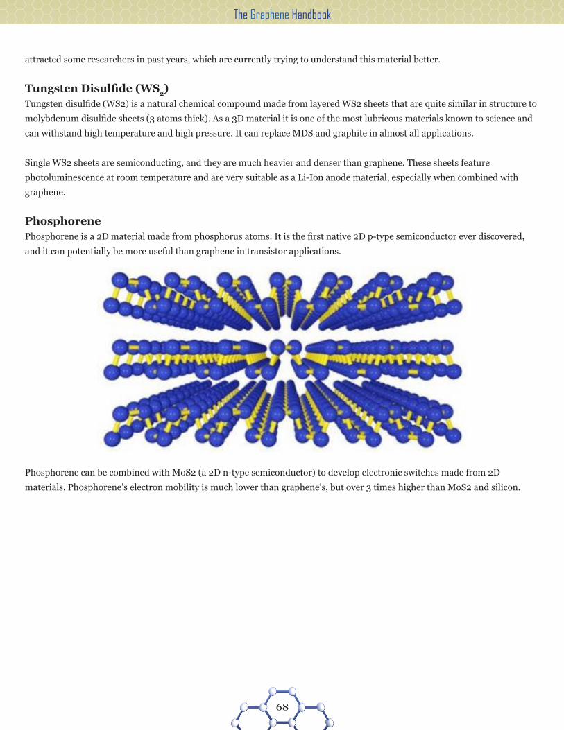
The Graphene Handbook
68
attracted some researchers in past years, which are currently trying to understand this material better.
Tungsten Disulfide (WS2)Tungsten disulfide (WS2) is a natural chemical compound made from layered WS2 sheets that are quite similar in structure to
molybdenum disulfide sheets (3 atoms thick). As a 3D material it is one of the most lubricous materials known to science and
can withstand high temperature and high pressure. It can replace MDS and graphite in almost all applications.
Single WS2 sheets are semiconducting, and they are much heavier and denser than graphene. These sheets feature
photoluminescence at room temperature and are very suitable as a Li-Ion anode material, especially when combined with
graphene.
PhosphorenePhosphorene is a 2D material made from phosphorus atoms. It is the first native 2D p-type semiconductor ever discovered,
and it can potentially be more useful than graphene in transistor applications.
Phosphorene can be combined with MoS2 (a 2D n-type semiconductor) to develop electronic switches made from 2D
materials. Phosphorene’s electron mobility is much lower than graphene’s, but over 3 times higher than MoS2 and silicon.

The Graphene Handbook
69
Appendix D: Company list
2-D Tech2-DTech makes and supplies 2D materials, including CVD-made graphene, graphene platelets, graphene oxide and other 2D
materials. The company also offers prototyping of graphene based devices.
2-DTech was spun-off by the University of Manchester and was acquired by advanced engineering materials maker Versarien
in April 2014 for £440,000. The company signed an agreement to become a project partner of the National Graphene Institute
(NGI) in November 2014.
http://2-dtech.com
3D Graphtech Industries3D Graphtech Industries was established in 2014 by Kibaran Resources and 3D Group to research and develop graphite and
graphene applications for 3D printing. 3D Graphtech will source its graphite exclusively from Kibaran’s Tanzanian graphite
mine.
AbalonyxAbalonyx, founded in 2005 in Norway develops functional nano materials (nano-composites, nano-laminates and coatings)
based on graphene derivatives. The company’s main focus is functional coatings for the renewal energy sector. Abalonyx aims
to build an IP portfolio for future licensing and production.
Abalonyx developed a new scalable process (modified version of the Hummers method) for the efficient production of high
purity Graphene Oxide. The company planned to launch its mass production (8 ton/year) facility in Q3 2014, in collaboration
with Kongsbert Innovasjon (we do not know if the facility is already online)
http://abalonyx.no
ACS MaterialACS Material is a US-based company focused on advanced nanomaterials development and production. The company offers
CVD grown graphene (single-layer graphene, graphene oxide, graphene nanoplates, carboxyl graphene and graphite oxide).
http://acsmaterial.com
AdNano TechnologyAdNano Technology, based in Karnataka, India, offers multi-wall carbon nanotubes (MWCNTs) and graphene sheets. The
company also offers related analytical services.
http://ad-nanotech.com
Advanced Graphene ProductsAdvanced Graphene Products (AGP) is a private company based in Poland that is focused on high quality graphene and
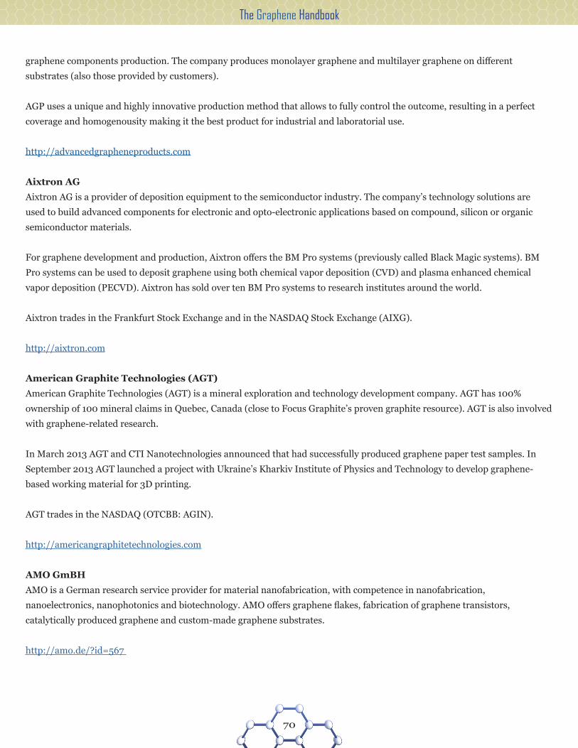
The Graphene Handbook
70
graphene components production. The company produces monolayer graphene and multilayer graphene on different
substrates (also those provided by customers).
AGP uses a unique and highly innovative production method that allows to fully control the outcome, resulting in a perfect
coverage and homogenousity making it the best product for industrial and laboratorial use.
http://advancedgrapheneproducts.com
Aixtron AGAixtron AG is a provider of deposition equipment to the semiconductor industry. The company’s technology solutions are
used to build advanced components for electronic and opto-electronic applications based on compound, silicon or organic
semiconductor materials.
For graphene development and production, Aixtron offers the BM Pro systems (previously called Black Magic systems). BM
Pro systems can be used to deposit graphene using both chemical vapor deposition (CVD) and plasma enhanced chemical
vapor deposition (PECVD). Aixtron has sold over ten BM Pro systems to research institutes around the world.
Aixtron trades in the Frankfurt Stock Exchange and in the NASDAQ Stock Exchange (AIXG).
http://aixtron.com
American Graphite Technologies (AGT)American Graphite Technologies (AGT) is a mineral exploration and technology development company. AGT has 100%
ownership of 100 mineral claims in Quebec, Canada (close to Focus Graphite’s proven graphite resource). AGT is also involved
with graphene-related research.
In March 2013 AGT and CTI Nanotechnologies announced that had successfully produced graphene paper test samples. In
September 2013 AGT launched a project with Ukraine’s Kharkiv Institute of Physics and Technology to develop graphene-
based working material for 3D printing.
AGT trades in the NASDAQ (OTCBB: AGIN).
http://americangraphitetechnologies.com
AMO GmBHAMO is a German research service provider for material nanofabrication, with competence in nanofabrication,
nanoelectronics, nanophotonics and biotechnology. AMO offers graphene flakes, fabrication of graphene transistors,
catalytically produced graphene and custom-made graphene substrates.
http://amo.de/?id=567

The Graphene Handbook
71
Anderlab TechnologiesAnderlab, based in Mumbai, India, is involved with carbon nanomaterial development and manufacturing.
The company developed a proprietary scalable graphene production technology, and they claim they can manufacture
graphene on a ton scale. They are also developing graphene inks and nanocomposites.
http://anderlab.co
Angstron MaterialsAngstron Materials (owned by Nanotek Instruments and based in Ohio, USA) is developing and producing nano graphene
platelets (NGPs), and also provide pristine graphite and single layer graphene.
In June 2013, the company installed new dry rooms and the company announced it aims to raise an additional $8 million
to $10 million to scale up production and bring its technology to the marketplace. In June 2011 the company announced a
spin-off called Angstron Supercapacitor that will produce a new supercapacitor electrode material made from Graphene. The
company is also developing a graphene-modified lubricant, Li-Ion battery materials and graphene-enhanced Polymers.
http://angstronmaterials.com
Applied Graphene MaterialsApplied Graphene Materials (previously Durham Graphene Science) was established in 2010 as a spin-off from Durham
University to develop a new graphene synthesis method and produce graphene materials. AGM’s technology is a unique
patented scalable ‘bottom-up’ CVD approach to produce graphene. The company was founded by Dr. Karl Coleman from
Durham University.
AGM is a public company that trades in the UK’s AIM stock exchange (ticker: AGM)
http://AppliedGrapheneMaterials.com/
Archimedes Polymer Technologies Archimedes Polymer Technologies (established in 2008 in Cyprus) is a specialist developer of nanocomposite materials. The
company develops nanomaterials-based solutions for polymers, metals and ceramics. APT also offers graphene nanoplatelets.
APT is involved with several European projects that use graphene-based materials, including TransCond, which aims to
replace high volatile organic content in electrically conductive coatings.
http://archimedesinternational.eu
Asbury CarbonsAsbury Carbons, established in 1895 in New Jersey, US, claims to be the world’s largest independent processor and
merchandiser of graphite. Asbury mines, refines and markets graphite and a broad array of carbon-based products.

The Graphene Handbook
72
Asbury produces graphene and also sells natural graphite to companies involved with graphene.
http://asbury.com
AVANSA Technology & ServicesAVANSA Technology & Services, based in India, offers analytical testing and consultancy services for industries with emerging
nano- and micro-technology-based products. The company also provides a wide range of nanotechnology-based research
services and products.
The company offers direct material sales and supplies few-layer graphene, functionalized graphene, reduced graphene oxide
and also graphene in solvents.
http://avansa.co.in
BASFBASF, based in Germany, is one of the world’s largest chemical companies—with over 350 production sites worldwide. BASF
has been involved with graphene research since 2008 in collaboration with the Max Planck Institute. The company was also
producing CNTs, but they quit the CNT market in May 2013.
In September 2012 BASF and the MPI launched a joint R&D operation, the Carbon Materials Innovation Center (CMIC), to
research graphene and other carbon-based materials.
http://basf.com
Biogenic ReagentsBiogenic Reagents produces low cost, high-performance carbon products made from renewable resources. The company
produces activated carbon for mercury and emissions control, metallurgical carbon for iron and metals production and
thermal carbon for energy generation.
In August 2013 the company announced it has begun commercial production of a graphene-based “ultra-adsorptive carbon”
compound made from renewable biomass.
http://biogenicreagents.com

The Graphene Handbook
73
Bluestone Global TechBluestone Global Tech (founded in 2011) is a New York, US-based graphene producer. BGT offers high-quality, fully
customizable graphene on several substrates (quartz, copper, silicon and others). The company also offers graphene FETs.
In February 2013 the company announced the availability of 24” by 300” graphene-on-copper foils. BGT supplies graphene
sheets to Shanghai Powerbooster for flexible touch panels. In September 2013 BGT announced plans to collaborate with
Manchester University on several graphene projects. BGT will also establish a European headquarters and production plant in
Manchester.
http://bluestonegt.com
Bluevine Graphene IndustriesBluevine Graphene Industries (BGI) was established in 2014 in Indiana, US, to commercialize graphene petal production
technology developed at Purdue University.
BGI’s graphene petal materials are branded as Folium materials. The company developed Folium-based applications which
include biosensors and supercapacitors.
http://www.bluevinegraphene.com
Bora Bora ResourcesBora Bora Resources is an Australian based graphite exploration company with a suite of high grade graphite projects in Sri
Lanka. Bora Bora has an option to buy up to 50% in Sri Lanka’s RS Mines, which owns several 99.99% natural high purity
crystalline vein graphite mines in Sri Lanka. RS Mines is also producing and marketing defect free graphene and graphene
oxide products.
In June 2014, BBR signed an agreement to exclusively supply Monash University with graphite from its Matale Graphite
project in Sri Lanka. The same agreement also gives Bora Bora the exclusive commercialization rights.
BBR is a public company, trading in the Australian Securities Exchange (ASX: BBR).
BT-CorpBottom Up Technologies Corporation (BT-Corp) was established in 2012 in India with an aim to manufacture graphene and
multiwall CNTs, develop carbon nanomaterials based applications and provide consulting on nanotechnology issues.
BT-Corp currently produces lab-scale graphene, graphene oxide and related products. The company also sells CVD
manufacturing equipment.
http://www.bt-corp.co

The Graphene Handbook
74
CalBattery CalBattery is a Los Angeles-based startup that develops silicon-graphene lithium-ion battery anode material. The company
develops materials and will also produce high-end batteries themselves in low quantities.
In September 2014, CalBattery introduced high-voltage, LCO cathode materials and high voltage electrolytes and also a new
generation carbon-nano material for advanced lithium battery applications.
http://clbattery.com
Calevia Calevia is a Canadian startup company established in August 2013 by Grafoid and ProScan Rx Pharma to co-develop
a graphene-based cancer thermal treatment platform. This new platform aims to overcome the side effects and strong
limitations of common cancer therapies.
http://calevia.com
Cambridge Graphene PlatformCambridge Graphene Platform (CGP) was established in March 2013 as a spin-off from Cambridge University to
commercialize graphene inks based on research work at Cambridge University. Graphene Platform is a major shareholder in
CGP.
CGP is developing a scalable and cost-effective method of graphene ink production based on a liquid phase exfoliation
technology that turns graphite into graphene in a water-based solution (without chemicals such as organic acids and without
thermal treatment). As CGP does not start with graphene oxide, this results in graphene inks with superior properties and
without chemical contamination.
Cambridge NanosystemsCambridge Nanosystems is a start-up company that was spun-off from the University of Cambridge with an aim to supply
graphene materials (and also Single‐Walled Carbon Nanotubes - SWCNT).
The company currently produces high quality (metal-free) graphene flakes (200-500 nm). The company’s capacity is several
kg/day, but they are now building a 5-ton factory in Cambridge.
In addition to the graphene flakes, the company developed graphene-based inks and is developing composite materials,
mainly for thermal management.
http://cambridgenanosystems.com

The Graphene Handbook
75
China Carbon Graphite GroupChina Carbon Graphite Group is a Chinese company based in Chengguan Town (Xinghe) that manufactures and sells graphite-
based products in China. CCG’s products include graphite electrodes, fine grain graphite blocks and high purity graphite. CCG
is also active in graphene technology research.
CCG trades in the NASDAQ’s OTC market (ticker: CHGI).
http://chinacarboninc.com
CientificaCientifica, established in October 2013 in the UK, focuses on graphene applications. The company plan is to acquire and build
businesses that make use of graphene materials.
Cientifica is a public company - they started trading on October 2013 in the UK’s AIM stock exchange (ticker: CTFA) after
taking over Avia Health Informatics shares and disposing of the old business. The company raised a net sum of £241,000
($389,000). We interviewed Cientifica’s CEO in December 2013. The company later to tried more money but failed, and
trading in their shares stopped in September 2014.
http://cientifica.com
CrayNano
CrayNano was spun off from the Norwegian University of Science and Technology (NTNU) to commercialize a new technology
to grow gallium arsenide (GaAs) nanowires on graphene using molecular beam epitaxy. The new hybrid electrode material
offers excellent optoelectronic properties.
http://crayonano.com
CTDATCTDAT was launched in 2014 in Mexico as a consultancy firm that specializes in graphene production technologies. CTDAT
developed a patent-pending process to exfoliate graphene from graphite.
The company is able to produce graphene oxide and reduced graphene oxide from ore mineral graphite. CTDAT is a private
company with close contact with Arizona University, UNAM and UNISON.
CTI NanotechnologiesCTI Nanotechnologies is developing graphene-related technologies. The company is collaborating with American Graphite
Technologies, and in March 2013 CTI and AGT announced they had successfully produced graphene paper test samples.
CVD Equipment CorporationCVD Equipment Corporation (based in Long Island, NY, US) offers a variety of process and support equipment for both R&D
and production facilities. CVD also offers graphene materials and other services for graphene production and processing.

The Graphene Handbook
76
In August 2013 CVD announced it will jointly develop graphene-based Li-Ion battery electrodes with Norway’s Graphene
Batteries. In 2014 CVD Equipment established in a new subsidiary (see below) called CVD Materials Corporation to offer
graphene and other nano materials.
CVD Equipment is a public company and trades in the NASDAQ (ticker: CVV).
http://cvdequipment.com/
http://products.cvdequipment.com/applications/cvdgraphene
CVD Materials CorporationCVD Materials Corporation, a subsidiary of CVD Equipment manufactures and sells nano materials. The company offers
monolayer graphene, multi layer graphene, 3D graphene, nanotubes and nanowires.
http://www.cvdmaterialscorporation.com
Directa PlusDirecta Plus was established in 2005 in Italy to develop innovative nanomaterial production processes. The company
developed thier own exfoliation process (which they call G+) that can be used to produce super-expanded graphite, pristine
GNPs, water-dispersed GNPs and fine nanographite powder (all of them marketed under the G+ brand).
In 2014, the company inaugurated its 30-ton graphene plant in Lomazzo, Como.
http://www.directa-plus.com
Focus GraphiteFocus Graphite (previously Focus Metals) is a mid-tier junior graphite company, mine developer and technology company
based in Ottawa, Canada. It is the owner of the highest grade (roughly 16%) technology graphite resource in the world (at Lac
Knife in Quebec). The company’s goal is to become an industry leader by becoming the lowest cost producer of technology-
grade graphite.
The company is collaborating on graphene research with Grafoid (of which it owns 40%). Focus Graphite is a public company
and trades in the OTC market (ticker: FCSMF).
http://focusgraphite.com
Future CarbonFuture Carbon, based in Germany, develops and manufactures carbon nanomaterials and carbon supercomposites. In April
2013, Future Carbon acquired several graphene and CNT related patents from Bayer.
http://www.future-carbon.de

The Graphene Handbook
77
Garmor Inc.Garmor Inc., based in Orlando, Florida, US, was spun off the University of Central Florida to develop a new cost-effective and
environmentally friendly graphene oxide flakes production process. Garmor aims to manufacture and sell graphene.
In April 2013 the company received $300,000 from the Institute for Commercialization of Public Research, and they plan to
open a production facility with a yearly capacity of 100 metric tons.
http://garmortech.com
GnanomatGnanomat, based in Madrid, Spain, developed a proprietary patented liquid-phase procedure to exfoliate graphite to
graphene. The single-step process produces high-quality graphene micro platelets. The process uses cheap, biodegradable
solvents.
The company seeks to find industrial partners to license the technology and scale it to an industrial scale.
http://www.gnanomat.com
Grafen Chemical IndustriesGrafen Chemical Industries, based in Turkey, was established in 2004 to develop and produce industrial materials including
nanomaterials, adhesives and engineering polymersin. Grafen claims to have developed a novel fabrication method allowing it
to synthesize graphene of excellent quality and with considerable yield.
In February 2013 Grafen signed an agreement with Angstron Materials for the supply of pristine and oxidized graphene for an
EMI application. In March 2014, Grafen raised 1.8 million from a Dubai-based investment company.
http://grafen.com.tr
Grafentek Grafentek, established in 2013 in Turkey, aims to mass produce graphene flakes to be used in Li-Ion battery anodes. The
company develops its own production technology. Grafentek also distributes Graphene Supermarket’s graphene products in
Turkey.
http://grafentek.com
GrafoidGrafoid is a private company based in Canada that produces graphene on a commercial scale using their proprietary extraction
process. The company is also active in high-growth, scalable graphene projects, graphene patents and material applications. In
May 2013 the company announced that they (together with Graphite Zero, of which it holds a majority stake) will start mass
production of affordable high-quality graphene materials under the MesoGraf brand.
Grafoid collaborates on graphene research with Focus Graphite (which owns 40% of the company). Focus Graphite also

The Graphene Handbook
78
provides Grafoid with its high-quality graphite. Grafoid is also co-developing graphene-based polymer and non-polymer
applications with Rutgers University. In July 2013 the company raised $3.5 million from private investors.
In August 2013 Grafoid established a new company called Calevia with Rx Pharma to develop a graphene-based cancer
treatment platform.
http://grafoid.com
GrafTech InternationalGrafTech International is a global company with more than 120 years of experience in the carbon and graphite industry.
GrafTech makes an expanded natural graphite foil that keeps most of the properties of the Graphene (thermal, electrical, and
possibly acoustic) and they manufacture them in flexible sheets from 20um to 1mm thick and in widths up to about 50 inches.
GrafTech say that their graphite-foil is used in Apple’s iPhone, Samsung’s TVs and many other devices. The company is public
and trades in the NYSE (ticker: GTI).
http://graftech.com
GRAnPH NanotechGRAnPH Nanotech (based in Spain) is a provider of single-layer graphene products and other carbon-based nanostructures
and nanocomposites. GRAnPH developed their own patented technology for producing graphene, based on research done at
the University of Alicante in Spain.
http://granphnanotech.com
GraphenanoGraphenano, based in Alicante, Spain and founded in 2011 is a graphene and carbon nanofiber producer that is collaborating
with the University of Castilla La Mancha in Ciudad Real. The company manufactures high quality graphene in industrial
quantity, with sheets sizes 50x50 cm.
In 2014 Graphenano launched a graphene-based paint called Graphenstone that is super-strong and can also help protect
buildings from environmental damage. According to reports Grapheneano is also gearing up to produce a graphene-polymer
battery in 2015.
http://graphenano.com
Graphene 3D LabGraphene 3D Lab, Inc was spun-off Graphene Labs in November 2013 to focus on development of high-performance
graphene-enhanced materials for 3D printing. The company aims to have a commercial graphene 3D printing filament
product in the market in 2015, and is also developing a 3D-printed graphene battery.
Graphene 3D Lab is a public company, trading in the Canadian stock exchange (TSX:GGG, OTC: GPHBF) following a reverse-

The Graphene Handbook
79
merger with Matnic Resources in August 2014. Lomiko Metals is a stakeholder in the company.
http://graphene3dlab.com
Graphene BatteriesGraphene Batteries, based in Norway, is developing safe and durable graphene-based high energy battery materials. The
company aims to build an IP portfolio and later license it for production.
In August 2013 Graphene Batteries announced it will jointly develop graphene-based Li-Ion battery electrodes with CVD
Equipment.
http://graphenebatteries.no
Graphene Corporationbecome a vertically integrated carbon company - from graphite mining to graphene production. The company has full
operational control and a 40% equity interest in Sakura graphite Mine in Sri Lanka.
Graphene Corporation is a public company that trades in the Toronto stock exchange (TSXV: ERA).
http://elcoraresources.com
Graphene DevicesGraphene Devices, founded in 2009 and based in Niagara Falls, NY, US, is a startup that explores novel uses for graphene and
ways to optimize its production. The company uses a process developed at the University of Buffalo.
Graphene Devices was awarded over $600,000 for several projects in 2010 by the US federal and state authorities. It is also
funded by Excell partners VC.
http://graphenedev.com
Graphene EnergyGraphene Energy is working toward next generation nano-technology-based supercapacitors that will have at least twice the
storage capacity of commercially available capacitors. Their technology utilizes graphene for the electrode material.
http://grapheneenergy.net
The Graphene Handbook
80
Graphene FrontiersGraphene Frontiers is a Pennsylvania-based startup established in 2011 based on new graphene-production technology
developed at the University of Pennsylvania. Graphene Frontiers uses an “Atmospheric Pressure Chemical Vapor Deposition”
(APCVD) roll-to-roll room-pressure process to synthetically grow graphene.
In September 2013 the company was granted $744,000 from the NSF to scale their production capacity.
http://graphenefrontiers.com
Graphene IndustriesGraphene Frontiers, based in Pennsylvania, US, was established in 2011 based on new graphene-production technology
developed at the University of Pennsylvania. Graphene Frontiers uses “Atmospheric Pressure Chemical Vapor Deposition”
(APCVD) roll-to-roll room-pressure process to synthetically grow graphene.
In September 2013 the company was granted $744,000 from the NSF to scale their production capacity. In July 2014, the
company raised $1.6 million and launched a new brand of highly-sensitive GFET-based biological and chemical sensors.
http://grapheneindustries.com
Graphene LaboratoriesGraphene Laboratories develops and markets functional graphene materials and devices. Graphene Labs operates two
online stores: Graphene Supermarket and Maximum Materials, which both offer online graphene-related products and other
advanced materials.
In February 2013 Graphene Labs signed a strategic alliance agreement with Lomiko Metals to co-develop a vertically
integrated supply chain and graphene-related products.
http://graphenelab.com
Graphene Leaders CanadaGraphene Leaders Canada (GLC) is a Canadian-based graphene supplier and application developer (mainly focused on the
energy sector at this time). The company developed their own graphite-exfoliation method to produce graphene and uses
Canadian mined graphite to produce GO and rGO materials.
GLC is currently selling to academia and research companies; however they plan to offer a web store for their graphene
products in 2014 and to engage industry for both materials and development services. Overall, their focus is to develop
application solutions to all industry sectors.
http://www.grapheneleaderscanada.com

The Graphene Handbook
81
Graphene NanochemGraphene Nanochem is a UK based company that manufactures performance specialty chemicals and advanced nanomaterials
from renewable sources including waste materials. The company offers several products for the oil and gas sectors.
Graphene Nanochem holds the exclusive license to a process known as Catalyx which uses a catalyst to extract graphene
from biogases (such as methane). This process can potentially mean low-cost graphene production. They are also developing
graphene-enhanced lubricants for used in the extraction of shale gas, graphene-based Li-Ion batteries and graphene water
treatment systems.
In September 2014, Graphene Nanochem signed a licensing and offtake agreement for the entire production of the graphene-
enhanced PlatDrill lubricant to Scomi-Oiltools, which is estimated at 135,000 tonnes over the next five years.
Graphene Nanochem started trading in the UK’s AIM stock exchange (ticker: GRPH) in March 2013 following a £32.5 ($50
million) fund raising.
http://graphenenanochem.com
Graphene Platform CorpGraphene Platform Corp (previously iTRIX), established in 2000 and based in Tokyo, Japan refocused its business to
graphene in 2011. The company maintains a fully equipped applications lab in Yokohama, Japan and produces CVD graphene
and epitaxial graphene on SiC for both commercial and R&D use.
GPC has a graphene subsidiary in the US called Graphene Platform Inc, and is also a major shareholder in Cambridge
Graphene Platform.
http://grapheneplatform.com
http://itrix.co.jp/graphene/index.html
Graphene SquareGraphene Square is based in Seoul, Korea, and was founded with the cooperation of Seoul National University. The company
provides CVD-grown graphene products and related products, accessories and services. Graphene Square also markets a
low-cost thermal CVD system enabling users to synthesize their own large-area, high-quality graphene samples in a lab
environment.
http://graphenesq.com
Graphene TechnologiesGraphene Technologies, founded in 2007 and based in Novato, California, US, developed a unique patented and eco-friendly
way to synthesize graphene (and other carbon-based materials) from carbon dioxide (CO2).
Graphene Technologies is planning to become a high-volume graphene producer, making both single-layer and few-layer
graphene sheets and other graphene-based materials. Their production process can produce graphene in all sizes: from large
The Graphene Handbook
82
sheets to small quantum-dots materials.
http://graphenetechnologies.com
Graphene-InfoGraphene-Info, based in Israel, is a web publication focused on graphene material technologies. Graphene-Info has been
providing services, information and resources for the graphene industry and researchers since 2009. The site is regularly read
by industry professionals, researchers, system designers and consumers interested in this promising new material and its
applications.
Graphene-Info is owned by Ron Mertens, the author of this book and the site’s editor-in-chief.
http://graphene-info.com
Graphenea
Graphenea is a privately-held company based in Spain that is focused on the production of high quality graphene for industrial
applications. The company produces single-layer graphene sheets, bi-layer graphene, multi-layer graphene, graphene oxide
and other materials—on any substrate the customer provides. The company is also involved with graphene application
research.
Graphenea is the main graphene supplier for Europe’s $1 billion Graphene Flagship project that was launched in October
2013.
http://graphenea.com
Graphenex
Graphenex is an R&D start up, established in 2014 and based in the UK that aims to develop prototype high energy
supercapacitors based on graphene materials. The company aims to develop the technology and then team up with
supercapacitor companies to commercialize it.
http://www.graphenex.co.uk/
Graphensic Graphensic was established in November 2011 in Sweden as a spin-off from the Linköping University. The company plans
to produce single-layer graphene on hexagonal silicon carbide for the electronic equipment market and related markets.
Graphensic’s technology uses a high temperature process to produce epitaxial graphene on SiC. The high temperature provides
better uniformity.
Graphensic is part of the LEAD business incubator, and in January 2013 the company raised $500,000 from LEAD.
http://graphensic.com

The Graphene Handbook
83
Graphite ZeroGraphite Zero was spun off the National University of Singapore (NUS) graphene center with an aim to develop and produce
MesoGraf graphene-based materials. The company uses Focus Graphite’s high quality graphite and transforms it into
economically scalable graphene products. Graphene Zero states it will soon start mass producing MesoGraf at a very low cost.
Grafoid holds a majority stake in Graphite Zero and handles the company’s business development and marketing.
Hangzhou GeLanFeng Nanotechnology
Hangzhou GeLanFeng Nanotechnology was established in 2011 to focus on graphene and related 2D materials.
GeLanFeng supplies monolayer and few-layer CVD graphene and MoS2 and also graphene flakes (GNP) powders, mostly to
University research teams and high-school students. The company also develops graphene applications and IP.
http://www.gelanfeng.net
Harbin MulanHarbin Mulan (the full company name is Harbin Mulan Foreign Economic And Trade Company) was established in 2000 in
China to supply carbon and graphite materials. The company provides monolayer flake graphene oxide, monolayer graphene
ultra-fine powder, graphene nanoplatelets, graphene oxide membrane (thin film), graphene solutions (dispersible in water,
DMF solvent) and more graphene-related materials.
http://sino-graphite.com
Haydale Haydale (a subsidiary of the ICL Group) supplies Split Plasma treated carbon materials - graphene flakes/GNPs, graphene-
based inks and CNTs. The company also offers customer R&D services and a lab for hire in the UK.
Haydale’s products are available online in their site in the UK, and their exclusive sales agent in the US is Cheap Tubes.
Haydale is a public company, trading in the UK’s AIM (ticker: HAYD).
http://haydale.com
IBMInternational Business Machines Corporation (IBM) is a multinational technology and consulting corporation based in the
US. IBM operates several research labs around the world and they are researching graphene related technologies - mostly
graphene based transistors and photo detectors.
In July 2014, IBM launched an ambitious 5-year $3 billion research initiative to find a silicon replacement for computer chips.
Graphene is one of the materials under consideration.
http://ibm.com

The Graphene Handbook
84
Incubation AllianceIncubation Alliance was established in 2007 in Kobe, Japan to manufacture and supply carbon materials. The company offers
so-called “graphene flower” materials: substrate-free and catalyst-free multi-layer graphene material made by direct synthesis.
It also offers graphene flowers dispersed in solvents, which are basically regular 2D graphene sheets.
http://incu-alliance.co.jp/en-index.html
IntelIntel Corporation, based in the US, is the world’s largest semiconductor chip maker (based on revenue). The company supplies
chips for PCs, mobile devices and more. Intel is researching graphene to be used in future electronic devices.
In September 2013 Intel’s CEO stated that the company was seeing “great progress” with graphene, but graphene-based
products were still “several generations away.”
http://intel.com
KNano KNano (the full name is Xiamen Knano Graphene Technology Co) is a start-up company based in China that mass produces
graphene nanoplatelets and is also involved with polymer-graphene composites. The company offers several types of graphene
platelets on their website.
http://knano.com.cn/En/index.aspx
LeaderNano (Jiling) LeaderNano, based in Jiling, China, develops and produces advanced nanomaterias - including graphene, graphene oxide,
nitrogen and boron doped graphene, GNPs and other materials (such as MoS2 and WS2).
http://eng.leadernano.com
LGLG Corporation, based in South Korea, is a multinational conglomerate corporation that is involved with electronics, displays
(LCD, plasma and OLEDs), telecom, chemicals and more.
LG has an active graphene research and holds many graphene patents.
http://lg.com

The Graphene Handbook
85
Lomiko MetalsLomiko Metals is an exploration stage Canadian company that aims to acquire and develop mineral resources in Canada. It
primarily explores graphite, zinc and gold. Lomiko owns several resource properties containing high-grade graphite, and the
company has signed a strategic alliance with Graphene Labs to co-develop a vertically integrated graphene supply chain.
Lomiko holds 15% in public Graphene 3D Labs Lab???, has a stake in newly formed graphene supercapacitor developer
Graphene ESD, and has also an internal graphene R&D department.
Lomiko Metals is a public company and trades in the TSX (ticker: LMR.V).
http://lomiko.com
Mason GraphiteMason Graphite is a Canadian mining company focused on the exploration and development of its 100% owned Lac Gueret
graphite project in northeastern Quebec.
In January 2014, Mason Graphite acquired 40% of graphene R&D company NanoXplore.
Mason Graphite is a public company, trading in the Toronto stock exchange (ticker: LLG).
http://www.masongraphite.com
Mega GraphiteMega Graphite was established in 2009 in Ontario, Canada with an aim to mine, process, purify and supply natural graphite.
The company holds four graphite mines in Canada as well as the Uley Graphite Mine in South Australia.
http://megagraphite.com
Moorfield Moorfield is a UK-based company, founded in 1989, that designs and manufactures a wide range of R&D-scale laboratory
systems. The company focuses on vacuum deposition products and CDV synthesis.
Moorfield’s nanoCVD systems offer compact, turn-key and scalable CVD systems for high-throughput graphene and CNT
production. Moorfield’s NanoCVD is exclusively distributed in the US by Graphene Laboratories.
http://moorfield.co.uk
http://nanocvd.co.uk
Morgan Advanced Materials Morgan Advanced Materials, based in the UK and founded in 1856, is an advanced materials technology company with a
global presence. The company is active in many markets, including medical instruments, aerospace, power generation and
trains. It is also active with carbon processing for over 150 years.
The Graphene Handbook
86
In August 2014, Morgan Advanced Materials signed a joint-development agreement with the University of Manchester to
scale-up a new graphene manufacturing process.
MAM is listed on the London Stock Exchange (LON:MGAM).
http://www.morganadvancedmaterials.com
mPhase TechnologiesmPhase develops battery technologies. Its flagship product (not yet released) is the AlwaysReady Smart NanoBattery—which
offers reliability, extended life and safe disposal. mPhase is exploring the printing of its “Smart NanoBattery” using graphene
(and possibly other advanced materials).
http://mphasetech.com
MTI CorporationMTI Corporation, based in California, US, was established in 1994 to manufacturer oxide crystals and substrates. The
company also offers lab equipment and furnaces—and they have a range of tube furnaces for graphene growth.
http://mtixtl.com/tubefurnaceforgraphene.aspx
Nanjing JCNanoNanjing JCNano, based in Nanjing, China, produces and supplies several carbon-based materials including graphene,
graphene oxide, graphite oxide and carboxyl graphene. The company started producing graphene in 2009 using a CVD
process.
http://jcno.net/index.php?langid=en
Nano Carbon (Poland)Nano Carbon was established in 2011 in Poland to engage in graphene research and production. The company uses technology
developed at the Institute of Electronic Materials Technology in Warsaw and is co-owned by mining giant KGHM and the
Polish Armaments Group (PGZ)
Towards the end of 2013 Nano Carbon started commercial production, and they offer their graphene materials via their on-
line store.
http://www.nano-carbon.pl
NanoCarbon Pty LimitedNanoCarbon Pty Limited was established in 2014 in Australia with an aim to commercialize graphene technologies developed
at the University of Wollongong. The technology is related to the manufacturing surfactant-free graphene, and the company
hopes to build the first pilot production line by July 2015.

The Graphene Handbook
87
The company will also be involved with graphene applications - such as high barrier films, lithium ion batteries, and water
purification.
NanoGrafenNanoGrafen was established in 2013 in Turkey as an nanotechnology R&D and consulting company. The company produces
high-quality graphene and develops graphene-based applications.
NanoGrafen also provides technical consultancy about the development of graphene based composites, the preparation of
masterbatches and formulation developments.
http://www.nanografen.com.tr
NanoInnova TechnologiesNanoInnova Technologies is based in Madrid and was spun off the Universidad Autónoma de Madrid. NanoInnova designs,
develops and commercializes instrumentation and nanostructured surfaces for research groups. The company offers
graphene-oxide, reduced graphene-oxide and other materials.
http://nanoinnova.com
NanoIntegris NanoIntegris (a subsidiary of Raymor Industries) produces, purifies and processes several grades of conductive carbon, carbon
nanotubes and few-layer graphene flakes. The company uses different exfoliation methods to produce the graphene.
Nanointegris service the industrial and academic R&D market with over 600 clients worldwide.
http://nanointegris.com
NanoXplore NanoXplore was established in 2011 in Canada with an aim to provide carbon nanomaterials (including graphene) services
and products.
NanoXplore is currently focused on their own graphene production method. NanoXplore says that their proprietary technique
to produce graphene from graphite is a low-energy, low-cost and scalable electrochemical conversion process.
Mason Graphite holds a 40% stake in the company.
http://nanoxplore.ca
National Graphite CorporationNational Graphite Corporation (NGC), based in the US, is focused on bringing the Chedic Graphite Mine back into commercial
production. In June 2013 NGC signed an agreement with American Graphene to jointly explore graphene opportunities and
The Graphene Handbook
88
employ a new sonication process to reduce graphite to graphene.
NGC is a public company (OTCQB: NGRC).
http://nationalgraphitecorp.com
National NanoMaterialsNational NanoMaterials was established in 2010 to commercialize technology developed at Texas State University and to
produce high quality nano materials. The company offers functionalized graphene materials under the Graphenol brand.
Graphenol can be supplied with amine, amide, ester, carboxylic or hydroxyl functional groups. The product is delivered as a
dispersion in surfactant-free water or organic solvent as mostly single or double sheets.
National NanoMaterials also offers research assistance services.
http://nationalnanomaterials.com
Ningbo Morsh TechnologyNingbo Morsh Technology was established by Shanghai Nanjiang in 2012 in Ningo, Zhejiang. It uses technology developed at
the Chongqing Institute, which was licensed to Shanghai Nanjiang.
Ningbo Morsh Technology has an ambitious plan to establish a new production line that was supposed to begin production
toward the end of 2013 (we have no information regarding the status of this line). The new fab’s annual capacity is 300 tons
(and if it is online, it is the world’s largest graphene fab by far). Reports say the investment in that line exceeded 100 million
yuan ($16 million). Ningbo Morsh Technology supplies graphene to Chongqing Morsh Technology, which is building a
production line in Chongqing that will be used to produce 15” single-layer graphene films.
Chongqing Morsh aimed to begin production in early 2014 and supply those films to Guangdong Zhengyang, used to produce
transparent conducting films (TCFs) to be used as touch panels for mobile phones. The company’s capacity is about 10 million
touch panels in a year. As we said before, we do not know the status of this project.
http://morsh.cn
NokiaNokia, based in Finland, is a multinational corporation that was once the world’s leading mobile phone maker. Nokia Research
Center, with its 10 laboratories worldwide, is exploring new technologies mostly for mobility applications.
Nokia is involved with graphene research, and the company takes part in the European €1 billion Graphene Flagship research
project.
http://nokia.com
https://research.nokia.com
The Graphene Handbook
89
Northern Graphite CorporationNorthern Graphite Corporation is a Canadian mine development company. Its main asset is the Bissett Creek graphite project
located 100 km east of North Bay, Ontario. The company is also involved with graphene research.
Northern Graphite trades in the Canadian stock exchange (ticker: NGC) and in the OTCBB (ticker: NGPHF).
http://www.northerngraphite.com
Oxford Advanced SurfacesOxford Advanced Surfaces Group, based in the UK, designs, develops and manufactures advanced materials for surface
modification, adhesion promotion and nano-material applications based on its highly reactive chemical core platform
technology called Onto.
In March 2014, OASG announced that it is investigating the use of its Onto technology platform to chemically functionalize
graphene. OASG is a public company that trades in the UK’s AIM (ticker: OXA).
http://www.oxfordsurfaces.com
Perpetuus CarbonPerpetuus Carbon is a graphene producer based in the UK. In early 2014, the company announced that it will soon begin
graphene production with an capacity of 100 tons (which will be extended to 500 tons by the end of 2014).
The company makes surface modified graphene materials, tailed to customer specifications. The price of their graphene
materials is about £50 per kilogram. Perpetuus also conducts R&D (via its Perpetuus Research and Development subsidiary)
mostly focused on graphene inks. The company also develops transparent conductive flexible films, stress strain actuators and
printable coatable electrodes for use in lithium Ion batteries.
http://perpetuuscarbon.com
PicosunPicosun, based in Espoo Finland, was established in 2004 to develop Atomic Layer Deposition (ALD) reactors for micro- and
nanotechnology applications.
The company is developing ALD-based graphene deposition using their advanced PEALD (plasma-enhanced ALD) system.
http://www.picosun.com
PlanarTech
lanarTECH is a US-based company (with manufacturing in Korea) that offers economical process equipment, analytical
equipment and training services for emerging 2D materials (graphene, boron nitride, molybdenum disulfide, etc.).
PlanarTech also provides a wide range of process equipment for other nanomaterials, as well as market entry and business

The Graphene Handbook
90
development consulting services for the Asian market with a particular focus on Korea.
http://planartech.com
Qingdao Huagao Energy Technology
Qingdao Huagao Energy Technology was established in China to produce graphene materials and develop graphene
applications.
QHET current offers several types of graphene and graphene-oxide materials, and is exploring graphene applications in Li-IOn
batteries, supercapacitors and semiconductors. The company expects to have an annual production capacity of hundreds of
kilograms of single-layer graphene.
http://www.hgky.net/en
QuantumWise QuantumWise is a provider of software solutions for nanotechnology developers. The company works in close collaboration
with the Nano-Science Center at the Niels Bohr Institute of Copenhagen University.
QuantumWise offers a system of integrated software modules (called Atomistix Toolkit, or ATK) that can accurately calculate
properties associated with electron distribution and transport. It can be used to compute the spin transport in graphene and
magnetic nanowires.
http://quantumwise.com
R-NanoR-Nano, based in Portugal and owned by RichAnswers-Nanomaterials, supplies laboratory supplies for the graphene industry.
The company currently offers single-layer graphene sheets on silicon and copper.
http://r-nano.com
Redex Nano LabRedex Nano Lab (RNL), based in Ghaziabad, UP, India, was established in early 2011 with the aim of becoming a
nanotechnology pioneer. The company commercialized several nanomaterials, including CNTs and graphene products.
RNL currently produces graphene sheets and nanoflakes using CVD, and also offers customized production.
http://redexnano.com
RS MinesRS Mines (previously GS International & the RS Group), based in Sri Lanka, owns several 99.99% natural high purity
crystalline vein graphite mines in Sri Lanka - including their flagship mine, the Queen’s Mine. The company is also producing
graphite oxide (GO) products, offering them via an online store.

The Graphene Handbook
91
In June 2014, Australian graphite miner Bora Bora signed into a heads of agreement with RS Mines.
http://graphite.com.co
Saivens MaterialsIndia’s Saivens Materials provides high purity nano materials including CNTs, graphene and inorganic materials. Saivens’
graphene product, branded RexSheet, is a high purity (over 90%) graphene sheet with a customized aspect ratio, grown using
CVD.
http://saivens.com
SamsungSamsung Group, based in South Korea, is a multinational conglomerate company involved with electronics, mobile phones,
displays (LCD, Plasma and OLEDs), materials, insurance, finance, advertising, heavy industry and more.
Samsung is researching graphene and is the company with the most graphene-related patents in the world.
http://samsung.com
Shanghai SIMBATT Energy TechnologyShanghai-based SIMBATT Energy Technology is developing, producing and marketing graphene powder materials. SIMBATT
currently offers intercalated graphite, graphene oxide, graphene powder, doped graphene powder, graphene quantum dot and
other materials.
Towards the end of 2012, SIMBATT inaugurated their graphene production center that can produce 1-5 layer graphene
powder in kilograms.
http://www.simbatt.com.cn/en/default.html
SiNode SystemsSiNode Systems was established in 2013 to commercial a novel anode Li-ion battery technology developed at Northwestern
University. SiNode’s anode uses a composite material of silicon nano-particles and graphene in a layered structure.
In April 2013 SiNode was chosen as the top startup company in the 2013 Rice Business Plan Competition, and their grand
prize was valued at $911,400. In August 2014, the company announced a joint-development agreement with Merck’s AZ
Electronic Materials.
http://sinodesystems.com

The Graphene Handbook
92
SonySony, based in Japan, is one of the leading consumer electronics companies in the world. Sony is developing graphene
technologies - including a roll to roll production process that can produce graphene sheets up to 100 meters in length.
http://www.sony.com
Strategic Energy ResourcesStrategic Energy Resources (SER) is an Australian based explorer with a diversified portfolio of mineral assets. The company
is exploring and developing land land with prospective large discoveries in Western Australia, South Australia and Victoria.
In May 2014 SER announced it is resolved to focus on graphene related investments to move the company forward. The
company holds a stake in Valence Industries, also involved with graphene. SER is a public company trading in the Australian
stock exchange (ASX:SER).
http://www.strategicenergy.com.au
Talga ResourcesTalga Resources is an Australia-based miner company with gold assets in Australia and high-grade graphite resource in
Sweden. The company already produces small-scale graphene products (and even supplied some to European customers).
Talga currently can make small lab-scale graphene production. The company aims to start a pilot plant in Sweden, and start
larger sample size from mid-2015 and afterwards perhaps full-scale production. Talga Resources is a public company trading
in the Australian Stock Exchange (ASE: TLG).
http://www.talgaresources.com
The Sixth Element MaterialsThe Sixth Element Materials Technology company, based in Chengzhou, China, is developing and producing graphene flakes,
graphene oxide and related materials.
The company says their current graphene-powder production capacity is 100 tons per year, and they plan to increase it to
1,000 tons by 2016.
http://www.thesixthelement.com.cn/en
Thomas SwanThomas Swan is a privately held global chemical manufacturing company. The company produces a broad range range of
additives, resins and active pharmaceutical ingredients, custom manufacture work and advanced materials. The company
claims to be the world leader in the manufacture of single-wall carbon nanotubes.
In March 2014 Thomas Swan launched graphene powder and water/surfactant dispersed graphene nanoplatelets. The
company is also developing several graphene applications with support from the UK government. Thomas Swan has a pilot

The Graphene Handbook
93
graphene line (capacity 1Kg/day).
http://www.thomas-swan.co.uk
TW Nano MaterialsTW Nano Materials is a supplier of single- and multi-layer graphene oxide (GO) and functionalized graphene oxide (FGO). The
company reportedly supplies these materials to several industrial partners.
The company is headquarters in the US (California) with production facilities in China and Sweden.
http://tw-nano.com
United Nanotech InnovationsUnited Nanotech Innovations (UNI), owned by Darwish Bin Ahmed Group, is an India-based nano technology company that
produces graphene materials, MWCNTs, nano composites and also offers nanotechnology R&D services.
The company can supply graphene materials in large quantities (several tons per year).
http://www.unitednanotech.com
Valence IndustriesValence Industries is an Australian industrial manufacturing company that produces high grade flake graphite products.
In March 2014 Valence launched the Graphene Research Centre in collaboration with the University of Adelaide. Valence is a
public company that trades in Australia (ASX:VXL).
http://www.valenceindustries.com
Veeco InstrumentsVeeco Instruments makes process equipment for several markets. The company’s main business segments are LEDs (and
OLEDs), PVs and data storage. It also provides molecular beam epitaxy (MBE) products that can be used for graphene
deposition.
http://veeco.com
VG ScientaVG Scienta offers vacuum components, surface science instruments and complete design and manufacture of standard
and special vacuum systems for scientific use. The company was established as a merger between Vacuum Generators and
Gammadata Scienta.
For graphene (and other 2D materials), the company offers CVD deposition systems and also PVD and sputtering systems
based on metal evaporation using thermal cells or E beam.
The Graphene Handbook
94
http://www.vgscienta.com/productlist.aspx?MID=404
Vorbeck MaterialsVorbeck Materials is a US company that develops graphene-based inks for the printed electronics market called Vor-X.
Vorbeck Materials states that Vor-X and plastic or rubber composites feature extreme levels of strength, dimensional stability,
conductivity, and environmental resistance, opening new application and design possibilities.
The company’s ink was used in the first ever graphene-based product, the Siren anti-theft packaging device.
http://vorbeck.com
Vulvox Nanobiotechnology CorporationVulvox Nanobiotechnology Corporation, based in Long Island, NY, researches and develops manufacturing processes for ultra-
high-strength graphene materials for ballistic armor and structural materials applications. The company is also researching
other R&D applications in the areas of power generation, electric motors and high temperature materials processing.
http://vulvox.tripod.com
XG SciencesXG Sciences is a private company based in Michigan, US. XG Sciences develops and markets graphene nanoplatelets under
the xGnP brand. XGnPs can be used to replace CNTs at a lower cost. xGnP can also replace nanoclay and provide electrical
conductivity and improved mechanical properties. The company’s technology was developed originally at Michigan State
University.
In August 2013 XGS launched a new graphene-based anode material for Li-Ion batteries. In August 2012 the company started
production in their new 80-ton facility in Lansing, Michigan. In 2014 Samsung Ventures placed a strategic investment in XGS
as the two companies aim to co-develop graphene-enhanced batteries.
http://xgsciences.com
Xolve Xolve (previously Graphene Solutions) is a manufacturer of purified and size selected carbon nanotubes, graphene and
nanographene. The company is working to commercialize simple room temperature processing of graphene and other
nanoparticle composites, solutions and coatings.
In December 2010 Xolve raised $2 million from both strategic and financial investors.
http://xolve.com

The Graphene Handbook
95
XP Nano MaterialXP Nano Material was established in 1998 in China to develop and produce nanomaterials. The company currently produces
graphene, CNTs, nano powders and other materials.
http://nanocnts.com


![Synthesis, Properties and Potential Applications of Porous ...graphene. Shown in Fig. 2 is the band structure for graphene and hydrogenated porous graphene (HPG) [56]. For pure graphene](https://static.fdocuments.us/doc/165x107/5e69b1218c0b164bfe524e90/synthesis-properties-and-potential-applications-of-porous-graphene-shown-in.jpg)