the-eye.euthe-eye.eu/public/Books/Electronic Archive/HalsallLister... · PITMANBOOKSLIMITED...
191
Microprocessor Fundamentals 3 B-. FHalsall/PFUster »tci %
Transcript of the-eye.euthe-eye.eu/public/Books/Electronic Archive/HalsallLister... · PITMANBOOKSLIMITED...

MicroprocessorFundamentals
3B-.
FHalsall/PFUster»tci
%

U.UAunr<iose>
Morccvn

MicroprocessorFundamentals

MicroprocessorFundamentals
Fred Halsall
MSc, DPhil, CEng, MIEELecturer in electronics and computer science
Paul Lister
MSc r PhD, CEng, MIEE, MIEEELecturer in electronics and control
University of Sussex UKSchool of Engineering and Applied Sciences
Pitman

PITMAN BOOKS LIMITED128 Long Acre, London WC2E 9AN
Associated Companies
1'iiniiiii Publishing New Zealand Ltd, Wellington
PitniBii Publishing Pty Ltd, Melbourne
© F Halsall & P F Lister 1980
First published in Great Britain 19S0
Reprinted 198L 1982
All rights reserved. No part of this publication may be reproduced,
stored in a retrieval system, or transmitted, in any form or by any
means, electronic, mechanical, photocopying, recording and'or
otherwise without the prior permission of the publishers,
This book may not be lent, resold, hired out or otherwise disposed of
by way of trade in any form of binding or cover other than that in
which it is published, without the prior consent of the publishers.
This book is sold subject to the Standard Conditions of Sale
of Net Books and may nol be resold in the UK below the net price.
Printed and bound in Great Britain
at The Pitman Press, Bath
ISBN 273 01522 2

Contents
1 Computer Principles
1.1 Technology 1
1.2 Historical Development 3
1.3 Mode of Operation 4
1.4 The Binary System 5
L5 Basic Structure and Operation
Microcomputer Architecture
2.1 Introduction 10
2.2 The Microprocessor 10
2.3 Memory 1
1
2.4 Highway Structure 13
2.5 Memory Map 15
2.6 Address Decoding 15
2.7 Bus Control 16
10
Exercises 17
3 Introduction to Programming and Data Transfer 18
3.1 Introduction 18
3.2 Microprocessor Registers 19
3.3 Assembly Language 20
3.4 Classification of Instructions 20
3.5 Operand Addressing Modes 21
3.6 Data Transfer Instructions 22
3.6.1 Register addressing 22
3.6.2 Immediate addressing 23
3.6.3 Direct addressing 25
3.6.4 Register indirect addressing 26
3.7 The Intel 8085 Instruction Set 28

vi CONTENTS
3.8 The Assembly Process 28
3.8.1 Hand coding 29
Exercises 31
4 Data Manipulation 324.1 Introduction 32
4.2 Data Representation 32
4.2.1 Unsigned binary 32
4.2.2 Signed binary 33
4.2.3 Binary coded decimal 35
4.3 Arithmetic Instructions 35
4.3.1 Add instructions 36
4.3.2 Subtract instructions 38
4.3.3 Increment instructions 39
4.3.4 Decrement instructions 40
4.4 Multiprecision Arithmetic Instructions 41
4.4.1 16-bit arithmetic 41
4.4.2 Multiprecision arithmetic; the carry flag 424.5 BCD Arithmetic 44
4.6 Logical Operations 464.6.1 Logical AND 464.6.2 Logical OR 484.6.3 Exclusive-OR 484.6.4 Rotate 494.6.5 Compare 50
Exercises 50
5 Transfer of Control 525.1 Introduction 525.2 Jump Instructions 52
5.2.1 Conditional jump 535.3 Flowcharts 545.4 Subroutines 55
5.5 Stack Operations 625.6 Parameter Passing 625.7 Nested Subroutines 64Exercises 66
6 Digital Input and Output 676.1 Introduction 67
6.2 Digital Input and Output 676.3 Memory Mapped Input/Output 696.4 Programmed Input/Output 69

CONTENTS vli
6.5 Programmable Input/Output Devices 70
6.5.1 Handshake control 70
6.5.2 Port initialisation 71
Exercises 78
7 Analogue Input/Output and Interrupts 79
7.1 Introduction 79
7.2 Digital-to-Analogue Conversion 79
7.3 Ana!ogue-to-Digital Conversion 81
7.3.1 The Shannon sampling theorem 81
7.3.2 A counter-based ADC 82
7.3.3 Successive approximation ADC S3
7.4 Interrupts 86
7.4.1 Programming with interrupts 88
7.5 Multiple Interrupts 91
7.5.1 Interrupt priority levels 93
Exercises 97
8 Application Examples 98
8.1 Introduction 98
8.2 Basic Sequencing 98
8.2.1 A traffic light sequencer 99
8.3 Conditional Sequencing 103
8.3.1 A washing machine controller 103
8.4 Digital Clock 106
8.5 Waveform Generation 1 14
8.5.1 Piecewise linear interpolation 116
8.6 Temperature Controller 121
9 Development Aids 126
9.1 Introduction 126
9.2 Single Board Systems 126
9.2.1 Monitor commands 128
9.3 Development Systems 129
9.3.1 Assemblers 131
9.3.2 Compilers and interpreters 132
9.3.3 High-level languages 134
9.3.4 Editors 137
9.3.5 In-circuit emulators 137
Appendix I The Intel 8085 Instruction Set 140
Appendix 2 Binary Multiplication and Division 145
Appendix 3 Microprocessor Characteristics 156
Solutions to Exercises 164Index 177

Preface
The wide range of application areas of microprocessors has resulted
in many potential users of these devices having no previous know-
ledge of computer hardware or software (programming). It is for this
reason that this book has been written as a basic introductory text on
microprocessors and their applications, intended primarily for readers
who have no previous knowledge in this field.
Generally, the many books currently available on microprocessors
assume that the reader has a significant background knowledge of
cither digital hardware or software. Our approach has been to
attempt to present the essential character of microprocessors and
some of their associated application principles without resort to
excessive electrical detail. Our experience of both teaching under-
graduates and retraining engineers from industry is thai an introduc-
tion to microprocessor applications can be taught effectively with
little reference to hardware detail. This means that a broad spectrum
of engineers, from many different backgrounds, can see the relevance
of microprocessors to their speciality without having to master a
wide range of electronics.
We have tried to present the material in this way with the sup-
plementary objective of producing a volume that was not of a
deterrent size or price.
There are now many students in technical colleges, polytechnics
and universities being introduced to microprocessors at a very early
stage in their studies and consequently the approach we have taken
makes this book particularly suitable for recommendation for such
courses.
The book has been written to be read on its own but many of the
examples have been developed with a "hands-on'' experience prog-
ramme in mind using a single-board prototyping system. We have
been involved in the preparation and presentation of a number of
VI!!

PREFACE ix
"hands-on1
' introductory courses on microprocessors and many of the
program examples have been developed as a result of this experience.
The microprocessor referred to throughout the book is the Intel
8085. This device is compatible in many respects with the earlier
Intel 8080 and the derivative Zilog Z80 microprocessors and has
become an industry standard 8-bit microprocessor.
Most of the programs presented can be run, with little or no
modification, on an Intel SDK85 single board computer or the
MAT385 Microprocessor Applications Trainer manufactured by
Feedback Instruments Ltd of Crowborough, UK.The basic principles of operation of a digital computer and the
associated terminology are presented in Chapter L The bus structure
and elements of a microprocessor-based computer are then intro-
duced in Chapter 2. Chapters 3, 4 and 5 introduce the range of
instructions and associated programming techniques typically avail-
able with microprocessors. The elements of digital input and output
using a programmable input/output device are covered in Chapter 6.
Analogue input and output techniques are introduced in Chapter 7.
In Chapter 8 a range of simple application examples are presented
that exploit many of the principles and techniques discussed in the
earlier chapters.
The book attempts to illustrate the fundamental characteristics
which are applicable to any microprocessor by continual reference to
a typical one, thus avoiding the potentially confusing necessity to
describe the many small differences between one microprocessor and
another. An appendix has, however, been included which gives a
brief summary of some of the main features of some of the other
popular microprocessors which are currently available and, where
appropriate, to indicate how they differ from the Intel 8085.
Or F Halsall
Dr P F Lister
University of Sussex

To Rhiannon, Lisa, Richard, Muriel, Jenny and Ben

1 Computer Principles
1.1 Technology The microprocessor is the culmination of the developments which
have been taking place in semiconductor technology since the first
production transistors produced in the early 1950s. Basically, a
transistor is produced by adding impurities to a semiconducting
material, usually silicon. It was soon realised that, by adding im-
purities to different areas of the same piece of silicon, it was possible
to produce a number of interconnected transistors on the same silicon
"chip". This became known as an integrated circuit.
Digital integrated circuits in the early 1960s involved small-scale
integration tSSI), a typical circuit being a few logic gates. Later came
medium-scale integration (MSI) with a complete integrated circuit
counter or register possible. Further refinements and changes in
technology have resulted in large-scale integration (LSI) devices
being commercially available at low cost which are comprised of
more than 10 000 individual transistors on a single silicon chip.
In order that such a circuit is widely applicable it must be very
flexible; hence manufacturers have made these devices into parts of a
digital computer. A microprocessor is one such device that forms the
central part of a computer. Others include memory devices and
programmable input/output circuits. All these devices are produced
using the same semiconductor technology. The process consists of
several stages of exposing intricate patterns on regions on the surface
of the integrated circuit chip to gaseous impurities at high tempera-
ture. These regions are defined by a photographic procedure. The
impurities form the various parts of a transistor that are finally
interconnected by a metallisation layer that is etched into the conduc-
tor paths by a further photographic process.
A photomicrograph of a typical microprocessor chip is shown in
Fig. 1.1. After fabrication, the integrated circuit chip is mounted onto
a flat base containing a number of connection pins, and the terminal

2 COMPUTER PRINCIPLES
nana DDDDFig, 1.1 Photomicrograph of a microprocessor {Courtesy Intel Corp.)
(Approx, size 5 mm square by 1 mm thick)

COMPUTER PRINCIPLES 3
Hi ~*r- ^^^frafr^r1^^* i ^«^^^-
.
EL'76
Fig. 1.2 A microprocessor, memory, and programmable input/output device
(Approx, V7 times actual size}
areas on the chip are connected to the corresponding pins on the base
by means of small gold wires. The entire assembly is then scaled to
form an integrated circuit package.
A photograph showing a fully-packaged microprocessor is seen in
Fig. 1.2 together with integrated circuit memory and programm-
able input/output devices. These three components can be used to
form a complete and powerful computing system.
1.2 Historical
DevelopmentThe basic structure and mode of operation of the first digital compu-
ter was proposed by the mathematician Charles Babbagc in the late
I 830s. However, it was not until transistors were used to build them
did computers become sufficiently reliable for their full potential to
begin to be explored.

4 COMPUTER PRINCIPLES
Since the first transistor-based machine was produced, computers
have been used in an increasing variety of applications. These range
from very large systems such as those used by banks to maintain
customer accounts to quite small systems that may, for example, be
used by an individual to solve a complex engineering problem. Theadvent of the microprocessor, however, means that it is now possible
to have the power of a computer in a single integrated circuit, and
consequently the range of applications is now virtually unlimited. It is
widely predicted that in the near future computers will be found in
almost every area of human endeavour. It is now possible to use a
microprocessor to control an automatic washing machine or a central
heating system or to control the exhaust emission from a car or the
operation of traffic lights -the list of possibilities is endless.
1.3 Mode of Basically, all digital computers operate in the same way which to a
Operation large extent is independent of the specific application to which they
are being put. This arises because a computer - large or small - is a
flexible general-purpose machine or device that can be arranged to
solve or implement a particular task after it has been produced by the
manufacturer.
A task is implemented by deciding the sequence of operations
needed to perform it. Consider a basic electronic calculator which
offers the user a variety of operations - add, subtract, multiply, etc. It
is then up to the user to select the particular sequence of these
operations necessary to solve a specific problem. Similarly a digital
computer can perform a number of basic operations called machine
instructions which the user selects and orders in a way which solves a
particular problem. This sequential list of operations is referred to as
a program.
An electronic calculator executes each of its basic operations in
typically a few milliseconds. Consequently the time taken to solve a
problem with a calculator is determined primarily by the rate at
which the user keys in the individual operations. The intrinsically
high speed of execution of each operation is therefore lost. A digital
computer, however, utilises the very high speed of execution of each
machine instruction - usually a few microseconds - by having the
required sequence of instructions, or program, stored within the
computer itself. This is known as the stored program concept and is
the fundamental difference between a basic calculator and a compu-ter system.
The information or data which is fed into a computer and the data
which is subsequently output by the computer varies considerably
with the wide variety of applications. In a mathematical application,

COMPUTER PRINCIPLES 5
the input and subsequent output information will perhaps be numeri-
cal, and the computer might simply perform some arithmetic opera-
tions on the input values. An application typical of those to which
microprocessor based computers are put is, for example, a
temperature-control system. Here the input data might be an indica-
tion of the controlled temperature and the output a signal to turn a
heating element either on or off.
Irrespective of the application, however, within the computer itself
the same means of storing and coding information is employed. In
order to achieve high levels of accuracy this coding is based on the
binary (two-symbol) system. Information stored using this system in
an electronic circuit is capable of being precise. This is because the
information is not dependent on the exact values of voltages and
current in the circuit provided these parameters can be unambigu-
ously interpreted as representing one or other of the two binary
symbols. All input data fed into a computer must first be translated
into a binary coded form, and similarly the subsequent binary coded
output must also be translated into the required form.
1.4 The Binary The binary system can perhaps be best explained by first considering
System a typical number in the decimal system. This system uses ten symbols,
0-9. The value of a symbol is weighted by its position in relation to
other symbols making up a number:
104
103 102 10 1 10° weighting
4 9 5 3 6 example
Thus 49536 = 4x 10⁴ + 9x 10³ + 5 xl02 + 3x10* + 6x10°. Each of the
five digits of this example is one of the ten symbols 0-9. Theweighting of each digit is a power of ten determined by the digit
position; hence decimal numbers have a base of ten.
Binary numbers are constructed in just the same way except that
they have a base of two. There are consequently only two symbols,
and 1, and digit weightings are powers of two:
24
23 22 21 2° weighting
10 111 example
Thus 10111 = 1x24 + 0x23 +1x22 + 1x2' + 1x2° which is equival-
ent to 23 in the decimal system.
All information within a digital computer is represented in a binary
form - both the input data to be manipulated and the coded instruc-
tions which control the various machine operations. The number of
binary digits or bits used to make up the basic unit of information in
a computer varies from one machine to another: for example 4, 8,
16, 24 and 32 bits have all been used in different machines.

6 COMPUTER PRINCIPLES
Microprocessor systems often use either 8 or 16 bits for the basic
unit of information or word. An 8-bit group is referred to as a byte.
So a 16-bit word is equivalent to two bytes.
When examining the operation of a microprocessor system, there-
fore, binary patterns are always being considered. This can be very
tedious for the programmer who is, when communicating this infor-
mation, prone to make errors. It is for these reasons that alternative
methods are often used to convey binary information between hu-
mans.
The method used is to group a number of bits together and then
represent that group with an equivalent coded number or character.
The most commonly used method is hexadecimal (base 16) coding
which is based on a 4-bit group. There are sixteen combinations of
four binary digits and hence sixteen symbols or characters are re-
quired. The sixteen symbols used are the ten numeric digits 0-9 plus
the six alphabetic characters A-F. The binary codes and correspond-
ing hexadecimal symbols are shown in Table 1.1.
Table 1.1 Hexadecimal numbers
4-bit binary pattern Hexadecimal symbol
0000
0001 1
0010 2
0011 3
0100 4
0101 5
0110 6
0111 7
1000 8
1001 9
1010 A1011 B
1100 C1101 D1110 E
1111 F
Some examples of binary patterns and their equivalent hexadeci-
mal (hex) representation are given below:
01101101 = 6D(hex) 11110010 = F2(hex)W '
i"
i
'
6 D F 2
1011010010001110 = B48E(hex)1
l"
l"
I"
i '
B 4 8 E

COMPUTER PRINCIPLES 7
1 .5 Basic
Structure andOperation
A digital computer executes a list of basic machine instructions (a
program) which have been selected and ordered by the user to solve
a particular task. In order to exploit the intrinsic high speed of
execution of each machine instruction, the program is stored within
the computer. In addition, all information stored within the
computer - both machine instructions and data -is represented in a
binary coded form. Thus a basic digital computer is comprised of a
memory which is primarily used to hold or store the program, a
microprocessor (often referred to as the central processor unit or
CPU) which executes the individual machine instructions which make
up the program, and some input and output (I/O) ports. These ports
form the interface between the computer and the source of the input
data and the subsequent output data. The complete combination of
microprocessor, memory and input and output ports is collectively
referred to as a microcomputer and is illustrated in Fig. 1.3.
MICROPROCESSOR(CPU)
Input/Output
Ports
cInputs
}Outputs
Computer Highway
Fig. 1.3 A microcomputer
Once the program has been evolved for the task, the complete
program is loaded into memory and is then executed. During prog-
ram execution, each machine instruction is accessed sequentially from
the memory and then executed by the microprocessor. The microp-
rocessor therefore operates in a two phase mode: during the first
phase, the fetch cycle, the next instruction is fetched from memory;
then, in the second phase or execution cycle, the microprocessor
executes (or performs) the action specified by the instruction.
In order to remember which program instruction is to be executed
next, the microprocessor contains a register (or temporary informa-
tion storage location) called the program counter (PC), the contents
of which points to the next sequential instruction to be fetched and
executed. Thus, during a typical instruction cycle, the next instruction
to be executed is read from the memory location indicated by the
contents of the program counter. While this instruction is being

8 COMPUTER PRINCIPLES
Program Counter
Stored Program
Instruction N
Instruction N+
1
Instruction N+2
Instruction N+3
a) The Program Counter Register
Fetch Execute Fetch Execute
Instruction N Instruction N+l
b) Fetch-Execute Mode of Operation
Fig. 1.4 Program execution
executed, the contents of the program counter are incremented to
point to the next instruction. This is summarised in Fig. 1.4.
Microprocessor instructions often require more than one byte of
information; usually 1, 2 or 3 bytes are required. Thus an instruction
fetch cycle may consist of up to 3 memory read operations performed
on successive memory locations. During the execution phase of this
instruction however, the program counter still points to the address
of the first byte of the instruction that would normally be fetched
next.
Exercises
1.1 Convert the following decimal numbers into their equivalent binary numbers:
35 67 224
1.2 Convert the following binary numbers into their equivalent decimal numbers:
10111 1010101 11011011

COMPUTER PRINCIPLES 9
1.3 Convert the following decimal numbers into their equivalent hexadecimal
number:
27 96 3334
1.4 Convert the following hexadecimal numbers into their equivalent decimal
numbers:
C3 2F 2C9E

2 Microcomputer Architecture
2.1 Introduction The basic functional units of a microcomputer were discussed in
Chapter 1. These comprise the microprocessor itself (the CPU), the
memory which is used primarily to hold the stored program, and
some input and output ports which are used to interface the mic-
rocomputer to the various input and output devices controlled by it.
2.2 TheMicroprocessor
The microprocessor can execute a number of basic machine instruc-
tions. Examples are individual data byte manipulation instructions
(add, subtract, etc.) and memory transfer instructions (read data byte
from memory, write data byte to memory, etc.). Information is
transferred between external devices and the computer system via the
input and output ports, and consequently the microprocessor has
machine instructions to both read (input) data from a specified port
and to write (output) data to a port.
Basically a microprocessor is comprised, as far as a user is con-
cerned, of the three sections shown in Fig. 2.1.
The register section contains a number of registers or temporary
storage elements which can each hold or store a single byte or word.
The arithmetic logic unit (ALU) performs the actual data manipula-
tion operations, and the timing and control section co-ordinates the
internal operation of the microprocessor and controls operation of
the ALU and registers so that the desired action specified by an
instruction is performed.
The microprocessor communicates with the memory, both to ob-
tain the individual instructions which make up the program and to
access and store data, and to transfer data to and from input and
output ports using a highway or bus.
More detail about the various microprocessor registers and their
use will be given in the next chapter.
10

MICROCOMPUTER ARCHITECTURE 11
MICROPROCESSOR
Registers
ALU
Timing &control
Highway
Fig. 2.1 A basic microprocessor
2.3 Memory The memory consists of a number of locations each individually
identified by an address. Each location contains a binary pattern with
a number of bits corresponding to the word length of the computer(typically 8 bits). The binary pattern stored at an address is referred
to as the contents of that address. In a microprocessor system the
memory is usually comprised of two types: random access memory(RAM) and read only memory (ROM). Basically RAM (more ap-
propriately called read/write memory but universally referred to as
RAM) has the capability of having information both written into and
read out of each location and is often used for storing intermediate
results (data) during a computation. ROM has information fixed into
it either during its manufacture or by the user and consequently can
only be operated in a read-only mode.
For many dedicated microprocessor applications ROM is used to
hold the (fixed) program. It has the advantage of being non-volatile
which means that when its power supplies are removed the stored
information is not lost. RAM is normally volatile unless the special
design features of certain types are exploited. The memory pattern
programmed into a factory programmed ROM during its manufac-
ture cannot be changed and hence it is essential that the program to
be stored in it is correct and free from errors. This type of ROM is
widely used in large-volume applications since the cost per bit is then
very low.
Erasable programmable ROMs or EPROMs have a memory pat-
tern which can be changed by the user in a controlled manner, and
hence this is a particularly useful device during program develop-
ment. The memory pattern in an EPROM is erased either by
exposure to intensive ultraviolet light through a "window" on the

12 MICROCOMPUTER ARCHITECTURE
Fig. 2.2 A UV EPROM and PROM programmer
(Courtesy Intel Corp.)

MICROCOMPUTER ARCHITECTURE 13
integrated circuit itself-UV EPROM-or by applying a voltage to
specific pins on the integrated circuit - EAROM or electrically altera-
ble ROM. The new memory pattern is then written into the device
using special hardware called a PROM programmer. An example of a
UV EPROM and a commercially available PROM programmer is
shown in Fig. 2.2.
2.4 HighwayStructure
The computer highway consists of three separate buses: the data
bus, the address bus, and the control bus. This is shown in Fig. 2.3.
The data bus is used to carry the data associated with a memory or
input/output transfer and is typically 8 bits wide. The address bus is
used to specify the memory location or input/output port involved in
a transfer. The control bus is made up of the various control lines
generated by the microprocessor and other system components to
synchronise transfers.
MICROPROCESSOR
^ ( Inputs
_) Outputs
Fig. 2.3 Highway structure
The data bus of many computers and particularly microprocessor-
based computers is bidirectional. That is, the processor can write data
on to the bus lines to be read by, for example, a memory device or it
can read data from the bus presented by such a device. Hence data
can be transferred from the processor to a device or from a device to
the processor over a single set of data lines. This is a particularly
desirable mechanism in a microprocessor system since it is not
necessary for the microprocessor to have both data input and output
pins. A practical limit to the number of available pins on a micro-
processor integrated circuit makes it important for the manufacturer to
use those available efficiently.
It becomes possible to make a single pin a logic input and output
by incorporating, within the microprocessor logic output gates, a
third output state in addition to the normal and 1 signals. This third
state is a high impedance condition where the output is effectively

14 MICROCOMPUTER ARCHITECTURE
Logic input
Select
Fig. 2.4 A three-state output
-Output <
or 1 whenselect 1.
High impedancewhen select 0.
MICROPROCESSOR
Select
direction
Bus line
Memory or I/O
Select
direction
Fig. 2.5 A bidirectional bus line
switched off. A select input to the gate is used to force the output to
this off state. This is illustrated in Fig. 2.4.
Devices of this type can be used to form a bidirectional bus by
connecting them in the arrangement shown in Fig. 2.5. This is for a
single line of a bus.
The microprocessor end of the bus can be either an input or an
output (but not both simultaneously) depending on the direction
selection control. The same applies to the memory or input/output
end of the bus. Control signals ensure that the direction of data flow
at each end of the bus is synchronised.
The address bus consists typically of 16 lines on which a binary
coded address can be presented to a memory or input/output port.
The range of possible addresses is therefore from 0000 (hex) to FFFF(hex), i.e. 65 536 (decimal) separate addresses. Thus a typical micro-
processor can address up to 65 536 (decimal) memory locations each
containing 8 bits (or one byte) of information. The size of a computer
memory is often measured in units of 1024 (decimal) locations. This
unit is designated IK. Hence most microprocessor systems can have a
maximum of 64K memory locations (64 x 1024 = 65 536).

MICROCOMPUTER ARCHITECTURE 15
MemoryAddress (hex)
FFFF
8 bits
210020FF
20001FFF
080007FF
0000
not used
RAM
not used
ROM
Fig. 2.6 A typical memory map
2.5 MemoryMap
For many microprocessor applications it is not necessary to use all
the possible memory addresses in the system. The range of addresses
that are used and the type of memory in each range is indicated by a
memory map. A memory map for a small but typical microcomputer
system is shown in Fig. 2.6. The figure shows that the system has 2K(0000 ^07FF) bytes of ROM and 256 (2000 -» 20FF) bytes of
RAM.In a small system of this type it is possible to allocate some of the
unused addresses to input/output ports. Data can then be transferred
between the microprocessor and an input/output port using the same
machine instructions as are used for transferring data between the
microprocessor and a memory location. This technique is discussed in
Chapter 6.
2.6 AddressDecoding
Since there are a number of devices connected to the computer
highway - ROM and RAM chips, input/output devices, etc. - it is
necessary to ensure that only the device intended for the data
transfer responds when a request is made by the microprocessor. This
is accomplished by each device connected to the highway having a
chip-select (CS) control input, and only when this input is activated

16 MICROCOMPUTER ARCHITECTURE
m.s. bitsAddress
Decoder
m l.s. bits
Chip
Select
Address
Data
Control
Memory or
Input/Output
Device
Computer Highway
Fig. 2.7 Address decoding
does a device respond to the various requests issued on the control
bus.
The memory map, as previously described, is used to define the
address range of each device connected to the bus. Each device,
therefore, has an additional logic circuit associated with it which
detects when an address intended for that device is present on the
bus. This is known as an address decoder and its output is used to
activate the chip-select input of the device.
In practice only the most significant address bits need be decoded
since the least significant address bits are used by the device itself to
determine, for example, the specific location within the selected
memory device. This is shown in Fig. 2.7.
2.7 Bus Control The control bus incorporates the timing signals which are generated
by the microprocessor to synchronise information transfers between
the microprocessor and a memory or input/output port. Consider the
timing diagram shown in Fig. 2.8.
The figure illustrates the two control signals - read (RD) and write
(WR) - generated by the microprocessor during two successive in-
struction cycles. The example assumes both are single byte instruc-
tions: the first is a memory (or input port) read and the second is a
memory (or output port) write. The type of transfer - memory or
input/output - will be determined by the memory map and the
specific address output by the microprocessor during each execute
cycle.

MICROCOMPUTER ARCHITECTURE 17
Address
Data
RD
WR
Address N
Instruction
Fetch
Memory or I/O
port address
Data
Execute
Address N+l
Instruction
Fetch
Memory or I/Ox
.port address /
Data
Execute
Instruction N Instruction N+l
Fig. 2.8 Timing diagram
Exercises
2.1 Determine the maximum memory space for an 8-bit microprocessor which has
a 14-bit address word. Express your answer in K bytes.
2.2 A microcomputer system requires 4K bytes of ROM and 256 bytes of RAM.Determine the start and end addresses of each memory block if the two
memories are to occupy contiguous blocks of memory starting at address 0000hex. Express your answer in hex notation.
2.3 If the microcomputer system in 2.2 requires four additional input/output ports,
define suitable addresses for the ports assuming memory-mapped input/output.
2.4 A microcomputer system has the following memory map:
0000 -> 0FFF ROM2000 ->2 IFF RAM4000 -» 400F I/O
Determine the amount of ROM and RAM memory and the number of I/O
ports in the system.

3 Introductionto Programmingand Data Transfer
3.1 Introduction A microcomputer can conveniently be considered as a device which
reads binary coded information from its input ports, manipulates this
information according to a program stored within its memory, and
subsequently produces output information at its output ports. This is
illustrated in Fig. 3.1.
Binary coded
input
information
MICROCOMPUTER
*-
Stored
Program
J
Binary codedy output
information
Fig. 3.1 A microcomputer
The instructions which make up the program are those selected by
the programmer from the instruction set of the microprocessor in
order to perform the required task. Before a programmer is able to
either write or interpret the meaning of a program, it is necessary to
become familiar with the different types of machine instructions
which a typical microprocessor executes and to investigate their effect
on the total system. The aim of this chapter therefore is to introduce
the different types of machine instructions which are typically availa-
ble and to show how some simple programs can be evolved using
some of these instructions.
The microprocessor selected for example purposes in this and
subsequent chapters is the Intel 8085. This is a widely used device
and its architecture and instruction set are typical of an 8-bit micro-
processor.
18

INTRODUCTION TO PROGRAMMING AND DATA TRANSFER 19
3.2 Microprocessor
Registers
The majority of machine instructions available with a microprocessor
operate on or affect the state of various internal registers which makeup the microprocessor. Before a program can be written for a
particular microprocessor, therefore, it is necessary to acquire a
knowledge of those processor registers which are accessible or are
affected by the machine instructions. The main registers for the Intel
8085, for example, are as shown in Fig. 3.2.
Further explanation and use of these registers will be given as the
various machine instructions are introduced in this and subsequent
chapters.
A
B C
D E
H L
F IM
Stack Pointer SP
Program Counter PC
A is an 8-bit arithmetic register (accumulator).
B, C, D, E are four 8-bit general purpose registers.
F is an 8-bit flags register (modified by ALUoperations).
IM is an 8-bit interrupt control register.
HL are two 8-bit registers which are normally used to
form a 16-bit memory pointer.
SP is the stack pointer register — this contains a
16-bit memory address which displays points to
the top of a system stack.
PC is the program counter register which contains a
16-bit memory address which points to the next
instruction to be executed.
Fig. 3.2 Main registers in the Intel 8085

20 INTRODUCTION TO PROGRAMMING AND DATA TRANSFER
3.3 AssemblyLanguage
It is extremely tedious and time consuming to represent each
machine instruction in its binary coded form. A far more convenient
representation of an instruction is what is known as its symbolic
assembly language equivalent. When each instruction is represented
in this form, programs are far more readable (and hence understand-
able) but, since there is a one-for-one correspondence between an
assembly language instruction and a machine code instruction, it is
also very straightforward to convert between one form and the other.
All the programs which are presented in this and subsequent chapters
will be written in assembly language. The method used to convert
these to basic machine language form is described later in this
chapter.
A typical assembly language instruction has the following format:
LABEL: OPERATION MNEMONIC, OPERANDS COMMENTS
The LABEL is an optional symbolic address for the instruction
which, as will be seen in Chapter 6, is particularly useful for branch-
type instructions.
Each machine instruction is assigned a corresponding OPERA-TION MNEMONIC which effectively tells the programmer the
specific operation to be performed. OPERANDS is either a value on
which this operation is to be carried out or the memory location(s)
where the value(s) can be found.
The COMMENTS field is for optional comments and is simply to
facilitate understanding and enhance the readability of the complete
program and does not influence the machine code resulting from the
assembly instruction.
3.4 Classification Although a microprocessor may execute perhaps a hundred or moreof Instructions different machine instructions, each instruction can in general be
classified as being a member of one of just five groups. These groups
are
Data Transfer
Data Manipulation
Transfer of Control
Input/Output
Machine Control
Instructions in the data transfer group move data between the
various processor registers or between a processor register and a
memory location. For example,
MOV A, B
INTRODUCTION TO PROGRAMMING AND DATA TRANSFER 21
results in the contents of the B-register being transferred to the
A-register.
Instructions in the data manipulation group perform arithmetic
and logical operations on data which is either in a specified processor
register or a memory location. For example,
ADD A, B
results in the A-register (accumulator) containing the sum of its
previous contents and the contents of the B-register. All instructions
in this group normally modify processor flags.
Instructions in the transfer of control group include unconditional
and conditional (flag dependent) jump instructions and subroutine
call and return instructions. All instructions in this group act on the
program counter and indeed it is this group of instructions which
gives the stored program machine its great flexibility. For example,
JMP LABEL1
results in the microprocessor breaking its normal mode of sequential
instruction execution and instead jumping unconditionally to sym-
bolic address LABEL1 for the next instruction to be executed.
Instructions in the input/output group move data between the
various input/output ports of the system and an internal processor
register - usually the A-register. For example,
OUT 05
results in the contents of the A-register being transferred to output
port 05 (hex).
Instructions in the machine control group affect the state or modeof operation of the processor itself. Some examples to be discussed
include interrupt enable and disable, processor halt (wait for an
interrupt), and no operation instructions.
3.5 OperandAddressing
Modes
A typical machine instruction implies three addresses: two to specify
the location of the values to be manipulated (the source addresses)
and the third to specify the location where the result is to be stored
(the destination address):
Source 1\^^Operation —» Destination
Source 2
In order to reduce the number of different addresses required for
an instruction, however, if two source addresses are required the

22 INTRODUCTION TO PROGRAMMING AND DATA TRANSFER
destination address is usually the same as one of the sources. Conse-
quently, most microprocessors - including the Intel 8085 -only re-
quire a maximum of two addresses to be specified.
The above examples show that the specific source and destination
addresses used vary for different types of instruction. Data movement
instructions, for example, utilise the various processor registers or
memory locations as source and destination addresses, whilst other
instructions may typically specify an actual data value in place of an
address.
The type of source and destination addresses utilised by an instruc-
tion is determined by the instruction addressing mode and all micro-
processors provide a variety of different addressing modes. The range
of addressing modes provided by a particular microprocessor is
important since it can often result in considerable flexibility whenwriting a program and also leads to programs which require fewer
instructions to implement a given task.
The four main types of addressing modes used in microprocessor
systems are:
1
These are used primarily for
data transfer and manipulation
instructions which involve only
the internal processor registers.
These are used primarily for
data transfer and manipulation
instructions which involve the
system memory.
In order to give examples of the use of each of these types of
addressing modes, in this chapter we will consider some examples of
instructions from the data transfer group. Subsequent chapters will
introduce instructions from the other groups.
3.6 Data Perhaps the most basic machine instructions are those from the data
Transfer transfer group. These are generally referred to as the move or load
Instructions instructions and some examples using each of the above addressing
modes are described below.
3.6.1 Register Addressing
This mode is used to move data between the internal processor
registers, and hence the instruction source and destination addresses
specify which of these registers are involved in the transfer.
Direct (Extended)
Addressing
Register Indirect
Addressing

INTRODUCTION TO PROGRAMMING AND DATA TRANSFER 23
For example:
MOV B, AI source address (A-register)
destination address (B-register)
operation (MOVe data)
This results in the contents of the A-register being transferred to the
B-register. The contents of the A-register remain unchanged. This is
often written as:
(B)^(A)
where the brackets mean "contents of".
Another example:
MOV C, B
means move or transfer the contents of the B-register to the C-
register:
(C)«-(B)
In addition, there are a limited number of data transfer instructions
which involve combined 16-bit register pairs -for example, DE and
HL. A typical instruction is
XCHG
This results in the contents of register pair DE being exchanged with
the contents of register pair HL. This can be represented as
(DE) <-> (HL)
3.6.2 Immediate Addressing
With this mode, the source address does not specify a register or
memory location but instead the actual source data is contained
within the instruction itself and is therefore immediately available.
For example:
MVI A, FE(hex)
I source data
destination address
operation
This results in the data value FE(hex) in this example being transfer-
red to the A-register:
(A) <- FE(hex)
or A<-11111110(binary)

24 INTRODUCTION TO PROGRAMMING AND DATA TRANSFER
Similarly, a 16-bit register pair (BC, DE or HL) may be specified
as the destination address and consequently these instructions require
two bytes of immediate data.
For example:
LXI H, 802D
This results in the 16-bit register pair HL being loaded with im-
mediate data 802D(hex):
(H)(L) «- 802D(hex)
Another example:
LXI D, E627
which means
(D)(E)^E627(hex)
i.e. registers D and E are loaded as a pair.
Program Example 3.1: Register Data Transfer
The program example of Fig. 3.3 uses a combination of the above
instructions. The program loads a value into the A-register using
immediate addressing and then loads this value into two further
registers, B and C, using register addressing. Finally, register pairs
HL and DE are loaded using immediate addressing and their con-
tents exchanged using register addressing.
Assembly Instructions
COMMENTS*MNEMONIC OP1 OP2
MVI
MOV
MOV
LXI
LXI
XCHG
A
B
C
H
D
FE
A
B
802D
E627
(A) — FE (hex)
(B) - (A)
(C) - (B)
(H) (L) — 802D (hex)
(D) (E) — E627 (hex)
(D) (E) *- (H) (L)
Fig. 3.3 Program Example 3.1
*The COMMENTS field is not used, in normal programming practice, toexplain the action of an instruction which is assumed understood.

INTRODUCTION TO PROGRAMMING AND DATA TRANSFER 25
3.6.3 Direct Addressing
Using direct addressing, an operand may be either read from or
written to a memory location, the address of which is specified in the
instruction itself. Since all memory addresses are 16-bits, the address
requires two bytes and it is for this reason that this mode is often
referred to as extended addressing.
For example: LDA 20EA
This results in the A-register being loaded with the contents of the
memory location with address 20EA(hex) and is expressed as
(A) <- (20EA)
Similarly, the contents of the A-register may be stored in a
specified memory location.
For example: STA 20F2
This results in the contents of the A-register being stored in memorylocation 20F2(hex) and is expressed as
(20F2) <- (A)
As the next section will show, the register pair H and L is
frequently used to hold a combined 16-bit memory address and
consequently two instructions are provided to enable the two regis-
ters (H and L) to be loaded using a single instruction and direct
addressing:
For example: LHLD 20A2
This results in register L being loaded with the contents of memorylocation 20A2 and register H being loaded with the contents of the
next consecutive memory location, i.e. 20A3 in this example. This is
therefore expressed as
(L) <- (20A2)
(H) <- (20A3)
Similarly SHLD 20AF
This results in the current contents of register L being stored in
memory location 20AF and the contents of register H being stored in
memory location 20B0. This is expressed as
(20AF)^(L)
(20B0)^(H)

26 INTRODUCTION TO PROGRAMMING AND DATA TRANSFER
Assembly Instructions Action
MVI A, FF (A)— FF (hex)
STA 20A2 (20A2) — (A)
MVI A, EE (A) — EE (hex)
STA 20A3 (20A3) — (A)
LHLD 20A2 (L) — (20A2) i.e. FF (hex)
(H)— (20A3) i.e. EE (hex)
SHLD 20A4 (20A4) *- (L)
(20A5) — (H)
Fig. 3.4 Program Example 3.2
Program Example 3.2: Direct Addressing
The program of Fig. 3.4 uses a combination of immediate and direct
addressing, first to store immediate data into two consecutive mem-ory locations, then to load register pair HL with this data, and finally
to store the same data into a pair of different memory locations.
3.6.4 Register Indirect Addressing
Using direct addressing, only the A-register may be used to store or
load a value to or from memory. Thus if a value were to be stored in
a memory location from, say, the B -register, using direct addressing, it
would first be necessary to transfer the contents from B to A before
the store operation could be performed. A more efficient method,
therefore, is to use register indirect addressing since, with this mode,data may be transferred between any of the processor registers and
the system memory.
Using register indirect addressing, the operand is either read from
or written to the memory location, the address of which is currently
stored in the register pair HL. The instruction does not contain the
actual memory address itself, therefore, but instead implies that the
address to be used is currently stored in the HL register pair. Theactual memory address is therefore obtained indirectly.
For example: MOV A, MThis results in the A-register being loaded with the contents of the

INTRODUCTION TO PROGRAMMING AND DATA TRANSFER 27
memory location whose address is specified in registers H and L. This
is represented as
(A)^((H)(L))
Similarly MOV M, B
This results in the contents of the B-register being transferred to the
memory location whose address is in registers H and L. This is
represented as
((H)(L))<-(B)
In addition to being able to load immediate data into a specified
processor register, there is also an instruction to enable immediate
data to be stored directly into a memory location. Again the memoryaddress is stored in the register pair H and L. Thus
MVI M, FF
results in the value FF(hex) being stored in the memory location
whose address is in registers H and L. This is represented as
((H)(L))<-FF(hex)
Program Example 3.3: Register Indirect Addressing
The program of Fig. 3.5 uses a combination of immediate and
register indirect addressing. A memory address is first loaded into
registers H and L using immediate addressing and then a value is
loaded into this memory location using register indirect addressing.
Finally, the value is loaded into two further registers again using
register indirect addressing.
Assembly Instructions Action
LXI H,20A0 (L) — AO (hex)
(H) — 20 (hex)
MVI M, AA ((H) (L)) - AA (hex) i.e. (20A0)— AA (hex)
MOV B, M (B) — (20A0) i.e. (B) — AA(hex)
MOV C, M (C) — (20A0) i.e. (C) — AA(hex)
Fig. 3.5 Program Example 3.3

28 INTRODUCTION TO PROGRAMMING AND DATA TRANSFER
3.7 The Intel
8085 Instruction
Set
The instructions which have so far been introduced are by no means
the only instructions available in the data transfer group. Indeed,
they are intended only as examples from the complete list of instruc-
tions which is available. For instance, in the data transfer group there
are instructions to enable data to be transferred (moved) between any
pair of processor registers selected from A, B, C, D, E, H and L.
Similarly, immediate data may be loaded into each of these registers.
The aim of this and subsequent chapters is simply to introduce
examples of instructions from a particular instruction group, together
with their meaning and application areas, so that the reader is able
firstly to understand the function of each particular instruction group
and secondly to select those instructions from the group which are
required to perform a specific task. The complete list of instructions
which comprise the Intel 8085 instruction set is given in Appendix 1.
3.8 TheAssembly Process
A microprocessor executes instructions which are stored as binary-
coded numbers in its program memory. Consequently, before any
programs can be executed, including the examples above, they must
first be converted from symbolic assembly to the equivalent binary
form.
General purpose computer systems, whether mainframe, minicom-
puter or microprocessor based systems, usually incorporate a suite of
programs (system programs) which have been designed to translate
programs written in higher-level languages (source code) into
machine (object) code.
If a line of source program in a high level language (e.g. Fortran)
usually yields more than one machine instruction, this translation
program is called a compiler. If the compiler program runs on one
machine and generates machine code for another computer, it is
referred to as a cross-compiler. The compilation process is illustrated
in Fig. 3.6.
If a line of source program usually yields just one machine instruc-
tion, the translation process is called assembly and a program that
performs this process is called an assembler. Cross-assemblers run on
host machines and produce machine code output intended for
another computer. Further aspects of systems programs are discussed
in Chapter 9.
In many small microcomputer prototyping systems the resident
operating program (monitor) cannot perform a complete translation
process on an assembly language program and instead each instruc-
tion must first be converted into an intermediate hexadecimal form.
The monitor then translates each pair of hexadecimal characters into

INTRODUCTION TO PROGRAMMING AND DATA TRANSFER 29
Assembly Language Program
Source
Program
Hand Conversion
Hexadecimal Form1
Compiler
Programt Monitor Program
MachineCode
' '
Binary Machine Code
Fig. 3.6 The compilation process Fig. 3.7 The hand assembly process
the corresponding 8-bit binary pattern. Since the conversion from
symbolic assembly form to hexadecimal has to be frequently per-
formed by the programmer, the manufacturers list of machine in-
structions usually contains the corresponding hexadecimal code for
each instruction. The hand assembly process is summarised in Fig. 3.7.
3.8.1 Hand Coding
The list of instructions for the Intel 8085 in Appendix 1 shows that
each symbolic assembly language instruction requires from one to
three bytes in hexadecimal form. For example, the instruction
MOV A, B
requires a single byte:
(A)«-(B)
7
The instruction
MVI A, FE
requires two bytes:
3E
FE
(A) «- FE(hex)
Operation
Immediate data, e.g. FE(hex)
Similarly, the instruction
STA 20F2
requires three bytes:
Operation32
F2
20
least significant byte of memory address
most significant byte of memory address

30 INTRODUCTION TO PROGRAMMING AND DATA TRANSFER
LINENo.
MEMORYLABEL
ASSEMBLYCOMMENTS
ADDRESS CONT MNEMONIC OP1 OP2
1
2000 3EMVI A FE (A)— FE (hex)
2001 FE
2
2002 47 MOV B A (B) - (A)
3
2003 4F MOV C B (C) - (B)
4
2004 21
LXI H 802D (H) (L) — 802D (hex)2005 2D
2006 80
5
2007 11
LXI D E627 (D) (E) — E627 (hex)2008 27
2009 E6
6
200A EB XCHG (D) (E) - (H) (L)
Fig. 3.8 Hand coding example
As an example of the hand coding process, Fig. 3.8 shows program
example 3.1 in both assembly language and hexadecimal form. Theprogram is assumed to be stored in memory starting at address
2000(hex).

INTRODUCTION TO PROGRAMMING AND DATA TRANSFER 31
Exercises
3.1 Write an assembly language program to
i) load the B-register with immediate data 87 (hex)
ii) transfer this value into registers A and Ciii) load the D-register with immediate data 2F(hex)
iv) transfer this value into register Ev) load the HL register pair with immediate data 8EF2(hex).
3.2 Write an assembly language program to:
i) load the A-register with immediate data FF(hex)
ii) store this in memory at location 20FF(hex) using direct addressing
iii) load register pair H and L with immediate data 20FF(hex)
iv) load the B-register with the previously stored data using register indirect
addressing
v) transfer the data in the B-register to registers C and D using register
addressing.
3.3 List the above programs on a table similar to that shown in figure 3.8 and
obtain the hexadecimal code for each instruction using the information in
Appendix 1.
3.4 Derive the contents of processor registers A, B and C and the contents of
memory locations 2020, 2021 and 2080 after the following program has run
and obtain the hexadecimal code for the program from Appendix 1.
LXI H, 2020
LXI D, 2080
ALnuMVI A, 2AMOV M, AMVI A, 20
MOV B, AXCHGMOV M, BXCHGMOV C, MMOV A, CSTA 2021
HALT

4 Data Manipulation
4.1 Introduction Since microprocessors may be used in a wide variety of applications,
it is necessary to be able to represent data within a microcomputer in
a number of different forms. For example, in some applications a
simple unsigned binary representation is adequate but in others it
may be advantageous to represent the data in a binary coded dec-
imal form. This chapter, therefore, first describes the different
methods available for representing data within a microcomputer, and
then introduces some typical arithmetic instructions from the data
manipulation group to illustrate their use with each form of numberrepresentation.
4.2 Data
RepresentationBefore considering specific arithmetic instructions, it is necessary to
examine the different ways numbers can be represented in a mic-
rocomputer. In general, numbers may be represented in unsigned
binary, signed binary, or binary coded decimal (BCD) form. These
are considered in turn.
4.2.1 Unsigned Binary
Unsigned binary is the most basic and, for microprocessors, the most
common form of number representation. In this representation all
numbers are assumed positive and a byte is simply the 8 -bit binary
equivalent of the number. Some examples follow:
27
26 2 5
24
23
22
21 2° == weighting
1 1 1 1 = 43 (decimal)
1 1 1 =70
1 1 1 =161
1 1 1 1 = 204
32

DATA MANIPULATION 33
Thus the range of numbers (in unsigned binary form) for an 8-bit
microprocessor using one byte per number is from to 255; numbers
in excess of 255 must therefore be represented by two or more bytes.
4.2.2 Signed Binary
For some applications it is necessary to be able to represent both
positive and negative numbers. Moreover, when performing arithme-
tic operations on the numbers it is necessary to produce the correct
signed result. Thus with a signed binary form of number representa-
tion, one bit, usually the most significant, is used to indicate the sign
of the number.
The simplest form of signed binary representation is sign and
magnitude since in this form the most significant bit indicates the sign
(0 positive, 1 negative) and the other seven bits the magnitude.
For example: 0011010 = +26
1 1100100 = -100
Unfortunately, however, with this form it is not possible to perform
simple arithmetic operations on numbers and automatically produce
the correct signed result. It is for this reason that the two's comple-
ment form of representation is often used because, as will be shown
later, performing arithmetic operations on two's complement signed
numbers automatically produces the correct two's complement signed
result.
As before, with two's complement the most significant bit, S, of
each number is used as a sign bit:
m.s. l.s.
6 5 4 3 2 1
S = for positive numbers and zero
S = 1 for negative numbers
For positive numbers, the simple binary codes is used to represent
the number. For negative numbers, however, the number is rep-
resented in its two's complement form. To obtain the two's comple-
ment of a number, the number is first inverted (complemented) and
the resulting number incremented by 1.

34 DATA MANIPULATION
For example:
+ 15 = 00001111
11110000
-15=11110001
invert
increment
Another example:
+ 89 = 01011001
10100110
-89=10100111
invert
increment
Note that, after the complement process, the most significant bit is
automatically a 1. For an 8-bit microprocessor, therefore, the range
of possible one byte numbers is summarised in the Table 4.1.
Table 4.1 Two's Complement Representation
Decimal Two's complementnumber representation
+127 01111111
+3 00000011
+2 00000010
+ 1 00000001
00000000-1 11111111-2 11111110-3 11111101
127
128
10000001
10000000
Note from the table that the maximum positive number that can be
represented is +127 and the maximum negative number is —128.
When performing arithmetic operations on 8-bit two's complement
signed numbers, therefore, it is important not to exceed this range,
otherwise incorrect answers will be obtained. For example, (+68) +
(+76) will produce an incorrect result since the result (+144) exceeds
the maximum possible positive number with 8-bits (+127). Similarly,
(—68) — (+76) will also produce an incorrect result since the result
(—144) is more than the maximum possible negative number (—128).

DATA MANIPULATION 35
4.2.3 Binary Coded Decimal (BCD)
It is sometimes preferable in some applications to use decimal
number representation and arithmetic within the microcomputer; for
example, if the input data is from a decimal keypad and the subse-
quent output data drives a decimal display. Most microcomputers,
therefore, provide instructions for performing arithmetic on binary
coded decimal (BCD) numbers. BCD representation is a subset of
the hexadecimal system introduced earlier and is summarised in the
Table 4.2 BCD Code
Decimal d 9't BCD code
00001 0001
2 0010
3 0011
4 0100
5 0101
6 0110
7 0111
8 1000
9 1001
Table 4.2. Thus an 8-bit binary number may be used to store twoBCD characters.
For example: 1000 0110 = 86 (decimal)
01010001 = 51 (decimal)
Summarising, the programmer may choose one of three different
forms of number representation. It should be stressed, however, that
the type of representation being used is in many ways transparent to
the microprocessor since this simply treats the data as an 8-bit binary
pattern and it is the responsibility of the programmer to process andinterpret this data in a form necessary to solve the particular task.
4.3 Arithmetic The basic arithmetic instructions provided by a microcomputer are
Instructions add, subtract, increment, and decrement. In general, with the 8085,
these instructions always involve the A-register and either another
processor register or a memory location. Since programmers mayrequire to interpret the data within the microcomputer in dissimiliar
ways, a microprocessor contains a number of different forms of these
instructions so that data can be manipulated in the selected manner.
In addition, the microprocessor contains a number of flags (status or
condition bits) which are either set or reset depending on the particu-
lar arithmetic instruction being carried out and the programmer is

36 DATA MANIPULATION
m.s. 1.3.
1X1 * 1X1 > 1X1 CY
S = Sign Flag
Z = Zero Flag
AC = Auxiliary Carry
^
P = Parity Flag
CY = Carry Flag
= Bit not defined
This flag is meaningful when signed numbersare being used. It is set when the result of an
arithmetic operation is negative, i.e. the m.s.
bit of the A-register is a 1
.
This flag is set if the result of an arithmetic
operation on the A-register is zero, otherwise
it is reset. This is used with transfer of control
instructions.
This flag is meaningful when BCD numberrepresentation is being used. It is set when the
result of an arithmetic operation produces a
carry out from the least significant half of the
A-register.
This is used with logical operations; the flag
is set if the result of a logical operation (AND,OR, XOR) produces an even number of l's.
This flag is the carry out from the m.s. bit of
the A-register. For example, CY is set after an
ADD instruction if a carry out was generated
from the A-register.
Fig. 4.1 8085 flags register
able to use and interpret these flags in order to manipulate data in
the selected way.
The individual flag bits are grouped together to form the flag
register, F, and as an example the F-register for the 8085 is shown in
Fig. 4.1.
Some examples of arithmetic instructions are now given together
with their effect on the individual flags in the flag register.
4.3.1 Add Instructions
The addition of two bits is summarised by the Table 4.3.
Table 4.3 shows that, because the sum can only be or 1, a carry
may be generated which must be added to the next higher order pair

DATA MANIPULATION 37
Table 4.3 Add it on of Two Bits
Bit 1 Bit 2 Sum Carry
1 1
1 1
1 1 1
Table 4.4 Addition of Two Bits and a Carry-in
Bit 1 Bit 2 Carry-in Sum Carry-out
1 1
1 1
1 1 1
1 1
1 1 1
1 1 1
1 1 1 1 1
of bits. Thus when adding two binary numbers it is necessary to
consider not only each pair of bits but also the carry digit from the
previous pair.
Table 4.4 is a truth table which summarises all the possible
combinations of two bits and a carry-in and the resulting sum and
carry-out.
For example
AB
10011010
01010111
manCarry = 00111100
154 (decimal)
87 (decimal)
A + B - 11110001 = 24 1 (decimal)
All Add instructions on the 8085 use either register, immediate or
register indirect addressing and affect all the flag bits. Examples of
each addressing mode are given below.
Register Addressing
Example: ADD B
This results in the contents of the B-register being added to the
current contents of the A-register. The result is placed in the A-register and the contents of the B-register are unchanged:
(A)*-(A) + (B)
After an ADD instruction the individual flag bits are affected as
follows:

38 DATA MANIPULATION
S set if result is negative (i.e. m.s. bit of A is 1)
Z set if result is zero (i.e. contents of A are all Os)
AC set if carry generated from bit 3 (used with BCD arithmetic)
CY set if carry from bit 7 (i.e. m.s. bit)
P reset
Immediate Addressing
Example: ADI OF
This results in the immediate data OF(hex) being added to the
current contents of the A-register:
(A)«-(A) + 0F
All flags are affected.
Register Indirect Addressing
Example: ADD MThis results in the contents of the memory location whose address is
contained in the H and L registers being added to the current
contents of the A-register. The result is placed in the A-register:
(A)<-(A) + ((H)(L))
All flags are affected.
4.3.2 Subtract Instructions
The subtraction of two binary numbers is similar to addition except
that the carry is now replaced by a borrow. The subtraction of two
bits is summarised in the truth table given in Table 4.5. Both bit 2
Table 4.5 Subtraction of Two Bits and a Borrow-in
Bit 1 Bit 2 Borrow-in Difference Borrow-out
1 1 1
1 1 1
1 1 1
1 1
1 1
1 1
1 1 1 1 1

DATA MANIPULATION 39
and borrow-in are subtracted from bit 1 to produce the difference
and, if necessary, a borrow-out. For example,
A= 10011011 = 155 (decimal)
B = 01010111= 87 (decimal)
///////Borrow = 10001000
A-B 01000100 = 68 (decimal)
The subtract instructions are identical to the above add instructions
except that a subtraction operation is performed in place of the addoperation. Again, all flags are affected. The corresponding subtrac-
tion instructions for each of the above addition examples are
SUB BSUI OFSUB M
4.3.3 Increment Instructions
The increment instructions use either register or register indirect
addressing to increment the contents of either a processor register or
a memory location by unity. All flags except the carry flag are
affected.
Register Addressing
Example: INR Aresults in the contents of the A-register being incremented by unity:
(A)<-(A) + 1
In addition to being able to increment the contents of a single
register, a number of instructions are provided to increment the
combined contents of a pair of registers.
For example: INX H
This results in the combined contents of register pair H and L being
incremented by unity:
(H)(L)^(H)(L) + 1
This is particularly useful when accessing a series of values from
memory.

40 DATA MANIPULATION
Register Indirect Addressing
Example: INR MThis results in the contents of the memory location whose address is
contained in the H and L registers being incremented by unity:
((H)(L))«-((H)(L))+1
4.3.4 Decrement Instructions
These instructions are identical to the increment instructions except
that the contents of either the processor register(s) or memorylocation is decremented by unity. The corresponding decrement
instructions are
DCR ADCX HDCR M
Program Example 4.1: Unsigned Arithmetic
The program example of Fig. 4.2 uses unsigned binary numberrepresentation. The two registers A and B are first loaded with
immediate data and their contents are added together. A third numberis then subtracted from the contents of A using immediate addressing
and finally the new contents of A are decremented by unity.
As has been mentioned, the microprocessor is not aware of the
type of number representation being used by the programmer; it
simply performs the indicated arithmetic operation and it is the
programmer who represents and interprets the binary patterns in the
required way. This can be seen from the following example.
Assembly Instructions Action
MVI A, 53
MVI B, 3A
ADD B
SBI 8C
DCR A
(A) — 53 (hex) i.e. 83 10
(B) — 3A(hex) i.e. 58 10
(A)- (A) + (B) i.e. (A) — 141 10
(A) — (A) - 8C (hex) i.e. (A)— 1 10
(A) — (A) - 1 i.e. (A) —
Fig. 4.2 Program Example 4.1

DATA MANIPULATION 41
Assembly Instructions Action
MVI A, 23
MVI B, B8
ADD B
SBI DB
DCR A
(A)*- 23 (hex) i.e. +35 10
(B) — B8(hex) i.e. -72 10
(A)- (A) + (B) i.e. (A)*- -37 10
(A) — (A) - DB (hex) i.e. (A) —
(A) - (A) - 1 i.e. (A) - -1
Fig. 4.3 Program Example 4.2
Program Example 4.2: Signed Arithmetic
The program example of Fig. 4.3 is the same as Example 4.1 except
that the initial numbers have been changed to represent a positive
and a negative value and the final result is negative. Two's comple-
ment signed number representation is therefore used and particular
care should be taken to interpret the signs of the numbers in the
correct way.
4.4 Multiprecision Although 8 bits are sufficient to represent a data value for manyArithmetic microprocessor applications, some necessitate the use of 16 or moreInstructions bits. Most 8-bit microprocessors, therefore, provide a number of
arithmetic instructions for manipulating numbers of more than 8 bits.
4.4.1 16-bit Arithmetic
In Chapter 3 it was mentioned that the 8085 provides some data
transfer instructions for loading 16-bit (2 byte) immediate data into a
register pair—BC, DE or HL. There are also instructions for incre-
menting and decrementing the combined 16-bit contents of a register
pair and also for performing double length (16-bit) addition.
For example: INX B
This results in the combined contents of registers B and C being
incremented by unity. No flags are affected:
(B)(C)<-(B)(C)+1
For example: DCX D

42 DATA MANIPULATION
This results in the combined contents of registers D and E being
decremented by unity. No flags are affected:
(D)(E)*-(D)(E)-1
For example: DAD B
This results in the 16-bit contents of the register pair BC being added
to the 16-bit contents of the register pair HL. The result is placed in
the register pair HL. Only the carry flag is affected: it is set if there is
a carry out from the most significant bit of H during the addition
operation, otherwise it is reset:
(H)(L)<-(H)(L) + (B)(C)
4.4.2 Multiprecision Arithmetic; The Carry Flag
If more than 16-bit accuracy is required, there are no single instruc-
tions available for performing arithmetic operations and instead a
number of instructions must be used. For example, consider the
addition of two 24-bit (3 byte) numbers. Each number would require
three memory locations and also the total addition operation would
require three separate 8-bit additions as illustrated in Fig. 4.4.
l.s.
Number 1 byte 3 byte 2 byte 1
Number 2 byte 3' byte 2'
CY
byte 1
'
r- CY -
i r 1Result byte 3+3' +CY byte 2+2' +CY byte 1+1'
Fig. 4.4 Multiprecision arithmetic
Fig. 4.4 shows that it is also necessary to add the carry bit (CY)
when adding together the second and third pair of bytes. The 8085,
therefore, provides additional add and subtract instructions which use
the carry (or borrow) bit.
For example: ADC MThis results in the contents of the memory location whose address is
contained in registers H and L and the contents of the CY flag being
added to the contents of the A-register. The result is placed in the

DATA MANIPULATION 43
A-register and all flags are affected:
(A)^(A) + ((H)(L)) + (CY)
Another example: SBB MThis is the same as the above except that a subtraction operation is
performed:
(A)^(A)-((H)(L))-(CY)
Program Example 4.3: Multiprecision Arithmetic
The program example of Fig. 4.5 adds together the 24-bit (3 byte)
number which is stored in the three consecutive memory locations
starting at address 2080 to the 24-bit number which is stored in the
three memory locations starting at address 2083. The 24-bit result
replaces the first number.
Assembly Instructions Comments
LXI H, 2083 Initialise HL to contain 2083.
LDA 2080 1
ADD M > Add 1st pair of bytes.
STA 2080 J
INX H Increment HL.
LDA 2081 1
ADC M > Add 2nd pair of bytes together with carry.
STA 2081 J
INX H Increment HL.
LDA 2082 ]
ADC M [> Add 3rd pair of bytes together with carry.
STA 2082 J
Fig. 4.5 Program Example 4.3
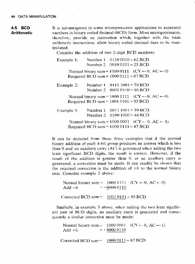
44 DATA MANIPULATION
4.5 BCD It is advantageous in some microprocessor applications to represent
Arithmetic numbers in binary coded decimal (BCD) form. Most microprocessors,
therefore, provide an instruction which, together with the basic
arithmetic instructions, allow binary coded decimal data to be man-
ipulated.
Consider the addition of two 2-digit BCD numbers:
Example 1: Number 1 0110 0010 = 62 BCDNumber 2 0010 0101 = 25 BCD
Normal binary sum= 1000 0111 (CY <- 0, AC <- 0)
Required BCD sum = 1000 0111 = 87 BCD
Example 2: Number 1 0111 1001 = 79 BCDNumber 2 0001 0110 = 16 BCD
Normal binary sum = 1000 1111 (CY<-0, AC «- 0)
Required BCD sum = 1001 0101 = 95 BCD
Example 3: Number 1 0011 1001 = 39 BCDNumber 2 0100 1000 = 48 BCD
Normal binary sum = 1000 0001 (CY <- 0, AC <- 1)
Required BCD sum= 1000 0111 = 87 BCD
It can be deduced from these three examples that if the normal
binary addition of each 4-bit group produces an answer which is less
than 9 and no auxiliary carry (AC) is generated when adding the two
least significant BCD digits, the result is correct. However, if the
result of the addition is greater than 9, or an auxiliary carry is
generated, a correction must be made. It can readily be shown that
the required correction is the addition of +6 to the normal binary
sum. Consider example 2 above:
Normal binary sum = 1000 1111 (CY <- 0, AC <- 0)
Add +6 = +0000 0110
Corrected BCD sum = 10010101 = 95 BCD
Similarly, in example 3 above, when adding the two least signific-
ant pair of BCD digits, an auxiliary carry is generated and conse-
quently a similar correction must be made:
Normal binary sum = 1000 0001 (CY <- 0, AC «- 1)
Add +6 = + 00000110
Corrected BCD sum= 1000 0111 = 87 BCD

DATA MANIPULATION 45
Thus the Intel 8085, for example, provides the following instruction
which may be used to automatically adjust the result produced by a
normal binary addition operation when BCD data is being manipu-
lated:
DAA (Decimal Adjust Accumulator)
This results in the 8-bit number in the A-register being adjusted to
form two 4-bit BCD digits by the following process:
1 If the value of the l.s. 4 bits of the A-register is greater than 9
or if the AC flag is set, 6 is added to the A-register.
2 If the value of the m.s. 4 bits of the A-register is now greater
than 9 or if the CY flag is set, 6 is added to the m.s. 4 bits of the
A-register.
Since both halves of the A-register are corrected and also both the carry
(CY) and auxiliary carry (AC) flags are affected, it is clearly possible
to perform multiprecision BCD arithmetic using the same instruction.
This is illustrated in the following example.
Program Example 4.4: BCD Arithmetic
The program example of Fig. 4.6 adds together two 4-digit (16-bit)
BCD numbers, and forms the corrected 4-digit BCD sum. The first
number is stored in the two consecutive memory locations starting at
address 2080 and the second is stored in the two locations starting at
address 2082. The result replaces the first number.
A correction must also be made when performing subtraction of
BCD numbers but it should be noted that this is different from the
correction required for addition. The correction can readily be de-
duced from examples and is summarised in Fig. 4.7. The table of Fig.
4.7 shows the state of the carry flags and the contents of the
A-register after the normal binary subtraction operation (SUB, SUI,
DCR) has been performed.
Two example subtractions are now given to illustrate the correc-
tions.
Example 1: Number 1 = 0100 0111 = 47 BCDNumber 2= 0011 0010 = 32 BCD
Normal binary difference = 0001 0101 (CY <- 0, AC <- 0)
Add 00 +0000 0000
Corrected BCD difference = 00010101 = 15 BCD

46 DATA MANIPULATION
Example 2: Number 1 = 1000 0001 = 81 BCDNumber 2= 0110 1001 = 69 BCD
Normal binary difference = 0001 1000 (CY «- 0, AC <- 1)
Add FA + 1111 1010
Corrected BCD difference = 00010010 = 12 BCD
The decimal adjust instruction of some microprocessors - the Zilog
Z80, for example - automatically performs the appropriate correction
after an addition and a subtraction operation by remembering the
type of arithmetic operation performed before the decimal adjust
instruction is executed. In other microprocessors - the Intel 8085, for
example - it is the responsibility of the programmer to determine and
perform the appropriate correction operation when performing sub-
traction with BCD numbers.
4.6 Logical So far in this and the previous chapter it has been assumed that the
Operations data within the microcomputer is always representing a numerical
value. In many applications, however, the data may simply be indi-
cating the state of, say, a controlled system. For example, a single
binary bit may indicate the state of a control valve: = valve open,
1= valve closed. Thus the 8-bit binary value 0110 0111 may mean
control valves 1, 2, 3, 6 and 7 are closed whilst control valves 4, 5
and 8 are open. In addition to the arithmetic instructions already
introduced, a microprocessor has available a number of data manipu-
lation instructions which are primarily included to manipulate non-
numeric data of this kind. These are the logical instructions and some
examples are now considered.
4.6.1 Logical AND
The logical AND instructions perform the bit-by-bit AND operation
between the contents of the A-register and either immediate data or
the contents of another processor register or a memory location.
The truth table for the AND function is shown in Table 4.6. Atypical application of this instruction is to test the state of a specific
bit in a group of, say, 8 bits.
For example: ANI 40
This results in the bit-by-bit logical AND operation between the
contents of the A-register and the immediate data 40(hex). The result
is placed in the A-register:
(A) <- (A) AND 40

DATA MANIPULATION 47
Assembly Instructions Comments
LXI H, 2082 Initialise HL to contain 2082.
LDA 2080
ADD M
DAA> Add 1st pair of bytes and form corrected sum.
STA 2080
INX H Increment HL.
LDA 208
1
ADC M
DAA> Add 2nd pair of bytes and form corrected sum.
STA 208
1
Fig. 4.6 Program Example 4.4
CarryCY
Upper hexdigit
(bits 7-4)
Auxiliary
carry
AC
Lower hexdigit
(bits 3-0)
Correction to
be added
1
1
0-9
0-8
7-F
6-F
1
1
0-9
6-F
0-9
6-F
00
FA
A0
9A
Fig. 4.7 BCD subtraction corrections
Table 4.6 AND Function Truth Table
Bit 1 Bit 2 Bit 1 AND Bit 2
1
1
1 1 1

48 DATA MANIPULATION
For example:
(A) = 0110 0100
40 = 0100 0000
(A) AND 40 = 0100 0000 P is reset (odd)
Thus if bit 7 of A was logical 1, the new contents of A are non-zero.
Conversely, if bit 7 of A was logical 0, the new contents of A will be
zero.
All logical instructions affect the parity flag P. If the number of Is
in the result (the new contents of the A-register) is odd, P is reset (0).
If the number of Is is even, P is set (1). Thus with the above example,
P is reset.
4.6.2 Logical OR
The logical OR instructions are similar to the AND instructions
except that the bit-by-bit OR operation is performed. The truth table
for the OR function is given in Table 4.7.
For example: ORA B
The contents of the A-register are OR-ed with the contents of the
B -register. The result is placed in the A-register:
(A)«-(A) OR (B)
For example:
(A) = 0110 0100
(B)= 1001 0101
(A) OR (B) = 11110101 P is set (even)
4.6.3 Exclusive-OR (XOR)
The exclusive-OR operation differs from the normal logical ORinsomuch that with the former, when both bits are logical Is, the
result is 0. The truth table for the exclusive-OR function is given in
Table 4.8. The range of exclusive-OR instructions provided are
similar to the OR instructions and are used extensively, for example,
in detecting and correcting errors that may occur when transmitting
binary information.
For example: XRA MThis results in the bit-by-bit exclusive-OR operation between the
contents of the A-register and the contents of the memory location

DATA MANIPULATION 49
Table 4.7 OR Function Truth Table Table 4.8 XOR Function Truth Table
Bit 1 Bit 2 Bit 1 OR Bit 2 Bit 1 Bit 2 Bit 1 XOR Bit 2
1 1 1 1
1 1 1 1
1 1 1 1 1
whose address is contained in the H and L registers. The result is
placed in the A-register:
(A)*- (A) XOR ((H)(L))
For example:
(A) =1001 1011
((H)(L)) = 1100 1101
(A) XOR ((H)(L)) = 0101 0110 P is set (even)
4.6.4 Rotate
The three previous instruction types - logical AND, OR and XOR -
performed the bit-by-bit logical operation between two 8-bit pat-
terns. In addition, the logical group contains instructions to rotate
(shift) a binary value left or right one place. This is useful, for
example, when performing binary multiplication and division: a left
shift is a times 2 operation and a right shift is a divide by 2 operation.
For example: RLC
The contents of the A-register are rotated left one place. The least
significant bit and the carry flag are both set to the value shifted out
of the most significant bit position. This is shown in Fig. 4.8.
CY UFor example (A) = 10010110
RLC (A) =/001 01 101*7 (CY) — 1
Fig. 4.8 Rotate left

50 DATA MANIPULATION
4.6.5 Compare
The compare instructions are often useful. They compare two
values - the contents of the A-register and either immediate data or
the contents of a processor register or memory location - without
modifying either value. The result of the comparison affects the flags
and, as the next chapter shows, these may be tested to determine the
next operation to be performed.
For example: CMP B
The contents of the B-register are compared with the contents of the
A-register. The Z flag is set to 1 if the contents are equal; the CY flag
is set to 1 if the contents of A are less than the contents of B.
Program Example 4.5: Logical Operations
The program example given in Fig. 4.9 first loads immediate data
into registers A and B and then performs a series of logical opera-
tions. First the contents of A and B are compared, the contents of Aare then rotated left, the new contents of A are then AND-ed with a
constant, and finally the resulting contents of A are OR-ed with the
contents of B.
Assembly Instructions Action
MVI A, F0 (A) — F0 (hex)
MVI B, OF (B) — OF (hex)
CMP B Z — 0, CY —
RLC (A) — El, CY — 1
ANI 81 (A) — 81, CY — 0, P — 1
ORA B (A) — 8F, CY — 0, P —
Fig. 4.9 Program Example 4.5
Exercises
4.1 Derive the equivalent decimal numbers from the following 8-bit binary patterns
interpreted in turn as unsigned binary, two's complement signed binary, and
binary coded decimal representations:
0110 1001
0010 1000
0111 0110
1000 1000
1001 0011
1000 0111

DATA MANIPULATION 51
4.2 Perform the following arithmetic operations using unsigned binary number
representation:
103 + 27
67+118105-9456-19
4.3 Perform the following arithmetic operations using two's complement signed
binary number representation:
-105 + 94
-56+19103-2767-118
4.4 Perform the following arithmetic operations using BCD number representation.
First perform the normal binary addition/subtraction operation and then add
the appropriate corrections derived in section 4.5:
34 + 52
19 + 27
75-4281-39
4.5 Determine the number which is in the A-register after execution of each
instruction in the following sequence:
MVI A, 13
ADI 41
DAA
4.6 Write an assembly language program to perform the following arithmetic
operation using two's complement signed binary number representation:
-56 + (-27)
4.7 Determine the result of performing the AND, OR and XOR logical operations
on the following pairs of bytes:
AE, 14
2B, 8F
37, 48A5. 5A
4.8 Determine the number which is in the A-register and the state of the
carry and parity flags after execution of each instruction in the following
sequence:
MVI A, 9EMVI B, A4RLCANI C2ORA B
5 Transfer of Control
5.1 Introduction The previous two chapters have been concerned with program in-
structions from the data transfer and data manipulation groups. Theflexibility and versatility of the stored program concept on which
computers are based, however, results primarily from the computer's
ability to transfer control, or branch, to an instruction that is not in
sequential order. This is achieved with instructions from the transfer
of control group. All these instructions act on the program counter
and, as will be shown, it is possible to execute a block of instructions
many times over with the number of times determined either by
program data or the state of, say, a processor flag.
5.2 JumpInstructions
A jump instruction is used to break normal sequential execution and
branch to a different part of the program. This is accomplished by
loading the address of the next out-of-sequence instruction into the
program counter, thus forcing the processor to fetch the contents of
this new location for its next instruction. This new address is usually
specified in the instruction. For example,
JMP 20B3
which in 8085 machine code looks like Fig. 5.1.
Execution of this instruction causes an unconditional jump to
memory location 20B3 for the next instruction. Thus if this instruc-
tion was stored in memory starting at address 2000, for example,
after execution of the instruction the program counter, instead of
containing 2003 (the start address of the next sequential instruction)
would contain 20B3.
When writing a program in symbolic assembly language, the abso-
lute address of the destination instruction is often not known until the
program has been fully developed. It is for this reason that the label
52

Memory address A
A+l
A+2
C3
B3
20
TRANSFER OF CONTROL 53
JMP operation
l.s. byte of address
m.s. byte of address
Fig. 5.1 Unconditional jump
Absolute Address
2000
20B3
Instruction
JMP LABI
LABI : Destination Instruction
-
Fig. 5.2 Symbolic addressing
field is provided with an assembly language instruction. A label is
used to indicate the destination address of a jump instruction and this
is only translated into its absolute hexadecimal form during the
assembly process. Thus the above instruction would take the form:
JMP LABI
where LABI is a label associated with the instruction stored at
memory location 20B3. This is illustrated in Fig. 5.2.
5.2.1 Conditional Jump
The above instruction is known as an unconditional jump instruction
since, when executed, a branch to the address contained within the
instruction will always occur. The real flexibility of jump instructions,
however, is derived from the conditional jump instructions since

54 TRANSFER OF CONTROL
Op-Code Condition Flag Status
JNZ not zero Z=0
JZ zero Z=l
JNC no carry c=o
JC carry C=l
JPO parity odd P=0
JPE parity even p=l
JP plus s=o
JM minus S=l
Fig. 5.3 Conditional jump instructions
these result in a branch for the next instruction only if a specified
condition is satisfied, otherwise the next sequential instruction is
executed.
The conditions which may be specified are determined by the state
of the various flags in the processor flag register. The conditions
which may be specified for the Intel 8085, for example, are shown in
Fig. 5.3.
Thus a typical conditional jump instruction is
JNZ LABI
This is read as: jump if zero-flag not set to LABI; and would result
in the next instruction being fetched from the address associated with
the label LABI only if the zero flag in the processor flag register was
not set (Z = 0), otherwise the next sequential instruction will be
fetched.
5.3 Flowcharts Before any program involving branching can be written, it is neces-
sary to plan the logical sequence of events to be carried out to
achieve the desired goal. A number of techniques may be used, but
the most useful for assembly language programs is the construction of
a flowchart. This is simply a diagram which indicates the sequence of,
and actions required in, a program and the points where branching is
required.
The symbols used in a flowchart are perhaps best illustrated by
means of examples.

TRANSFER OF CONTROL 55
Program Example 5.1: Flowcharts
Consider a simple program to add together the ten numbers 1-10. Aflowchart for this program is shown in Fig. 5.4.
Let the C-register contain the number to be added to the running
total and the B-register contain the running total.
The assembly language instructions given in Fig. 5.5 for the pro-
gram have been evolved using the flowchart of Fig. 5.4. The CPI
(compare immediate) and JNZ (jump not zero) instructions in Fig.
5.5 are used to determine when the count has reached 11. This
combination is frequently used to provide a conditional transfer of
control.
Program Example 5.2: Jump Instructions
A common requirement when a microcomputer is interfaced to other
equipment is to compute a time delay in the program. Amicrocomputer-based road traffic light controller, for example, would
need to compute a time delay to implement the sequencing of the
light changes.
Since each machine instruction takes a specific amount of time to
be executed (typically a few microseconds), it is possible to compute a
time delay by executing a group of instructions a preset number of
times. The delay obtained is then approximately proportional to the
number of times this group of instructions (or loop) is executed. Let
the desired delay and hence loop count be held in the C-register.
A flowchart for this program is given in Fig. 5.6. This flowchart can now
be readily translated into the assembly language program of Fig. 5.7.
The basic time delay is derived from the six no-operation instruc-
tions (NOP). These instructions do not affect any of the processor
registers or memory and the delay can be readily extended by
substituting them with different instructions. Note that the compare
and conditional jump instructions are again used to determine the
transfer of control.
5.4 Subroutines Frequently within a program it may be necessary to perform a
particular sub-task many times over. It is highly desirable not to have
to repeat the section of machine code each time the sub-task is
required. It is therefore necessary to be able to transfer control in a
program to a section of often-used code or subroutine designed to
perform the sub-task and then return control to the main instruction
sequence.

56 TRANSFER OF CONTROL
od
Ct3
< c
15^_
CQ<-J
CQ
"c3 c a O cOJj
OJ O 3O so c < ^
13.c CJ c 3 u 73c
c E 50 '£ C33J
X)
3 3 u c Oh>3
vs
c '5
c "£
5•ac
c 1—c u. P CJ O —
i
"c5 15 SO O so O i
£ ^ ^ C 0 ^ t- c c/3 c/3
o 'B0 OJ 'C « O a>
\JC
CQ < a: cq z >
to
.0 O „,
,
> O CQ < u CQ5 „ „ ~ „ , CQ <^ CQ U < U CO D < O -i>5
_ _ > Q > >O > > O Q O Z
NZs s S < S s
^to=0 CQ^ <
-1
Q.
ECO
XLU
ECO1—
OJo
E</>
CO
<in
in
6>
CO
O "*-•
SOn
c3
ac3*-i JO<u e
3C3 c^ •a
£ ccS
rt t-.
< JS
c QZ
§c ^ V^_yn^»*o
aECO
xUJ
tCO
JZo
o
in

TRANSFER OF CONTROL 57
ot/3 (/3
c «O X> a,
c u w x:oo
*2 >> o £ o csc 03 m v; T3 o^> r- •—ss
1>
T3
'3
a"1)
<03
Cocoo
*'i>
operation
ii
sed
to
prov
me
delay.
c
uOJ N 6 3 ~ -o
con u < z 'M
^^ A
^c•2
^ fN O w cu
35^
o o S oO
soSt u < U H u J<
1
^\ _ __ a. cu 0- Cu Cu cu cu Oi Cu-C5 > > ^ N O o o o O o U 55 S s z z z z z z Q^j<oto
X 0-
oo-J
uU
SH
CM
ir>
_a>
aECO
xUJ
ECOL.
3O
>
£CDCOCO
<
If)
t/5
co
u
(Oo
T3 C 2 «
z
oad
desire
elay
time
arameter
io IS
oc .S g>
*"
i
15 1 £
4J «h—l -a a < o
4) O
QZW
CN
LO
_Q)
aECO
XUJ
ECOl_
O)o
CO
.cu
I
(0
in
d)
ii

58 TRANSFER OF CONTROL
Subroutines not only save program memory because it is not
necessary to repeat a program section every time a sub-task is
required, but they also provide the opportunity to structure a pro-
gram into convenient sections that can be written and tested indepen-
dently and then collected together to perform the overall task.
The two basic instructions provided to call a subroutine and return
from it are
CALL nnnn
and
RET
where nnnn is the two-byte four hex character starting address of the
subroutine. The RETurn instruction is the last instruction to be
executed in the subroutine and it returns control to the calling
program at the instruction following the CALL instruction. This is
illustrated in the program memory diagram of Fig. 5.8. In assembly
language it is usual to indicate the start address of a subroutine by
Main
program
CALL SUB
SUB:
Subroutines
RLT
Fig. 5.8 Memory diagram illustrating a subroutine CALL

TRANSFER OF CONTROL 59
means of a label (symbolic name) and this is only translated into the
corresponding four hex character absolute address during the assem-
bly process.
When the microprocessor executes a subroutine CALL instruction,
in addition to transferring control to the start address of the sub-
routine, it must also remember the current address within the main
program so that it can return control to that point when the RETinstruction is executed. This is accomplished by saving the current
contents of the program counter register (PC) on a stack.
A stack is simply a last-in first-out queue which is implemented as
a set of successive locations either within the processor itself or, moreusually, in the system memory. The stack pointer register (SP) within
the processor always points to the address which currently holds the
entry at the top of the stack, and consequently its contents change as
each subroutine call and return instruction is executed. If the stack is
implemented in the system memory as on the Intel 8085, the initial
content of the stack pointer is arbitrary and it is usually initialised to
point to an unused area of memory.
The sequence of operations and the appropriate contents of the
stack pointer and program counter during a subroutine call are
illustrated in Fig. 5.9. It is assumed that the stack pointer (SP)
currently contains 20C2 and, as is shown, its contents are de-
cremented by two as the contents of the program counter (PC) - two
bytes - are saved when the subroutine call is executed.
Whenever a RETurn instruction is executed, the process illustrated
is reversed. The program counter is loaded (least significant byte first)
with the contents at the top of the stack, the stack pointer is
incremented twice, and control returns to the instruction following
the subroutine call. Subroutine call and return instructions are availa-
ble that are conditional in just the same way and for the same range
of conditions as conditional jump instructions.
Program Example 5.3: Subroutines
The previous program example was a short program to compute a
time delay. This can conveniently be made into a subroutine by
placing a RET instruction with the label TIME at the end of the
program. In order to make this subroutine useful for other parts of an
imaginary application program, it is desirable to set the delay time in
the main program and not in the subroutine itself. In this way the
same subroutine can implement a variety of delay times. To imple-
ment this, the C-register is used to pass the required time delay
parameter to the subroutine (TIMDLY). This is shown in Fig. 5.10.

60 TRANSFER OF CONTROL
Memory Address Contents Symbolic Instruction
MainProgram
2010
2011
2012
CD
48
20 !
> CALL SUB PC =
SP =
2013
1" 2048
Subroutine < 2049
XX
XX
SUB : Subroutine
Instructions
Stack <
20C0
20C1
20C2
XX
XX 20C2
(i) CALL instruction brought from memory — PC incremented
Memory Address Contents Symbolic Instructions
MainProgram
2010
2011
2012
CD
48
20
> CALL SUB PC =
SP =
2048
r 2048
Subroutine < 2049
XX
XX
SUB: -
Stack <
20C0
20C1
20C2
13
20
XX
20C0
(ii) PC contents saved and contents of SP decremented

TRANSFER OF CONTROL 61
Assembly Instructions Comments
I
LXI SP, 20C2 Initialise stack pointer.
Main J
Program ]MVI C, 02 Load TIMDLY parameter.
ICALL TIMDLY Call Subroutine.
"TIMDLY: MVI A, 00 Time delay subroutine.
LOOP: CMP C
JZ TIME
NOP
NOP
Subroutine <NOP
NOP
NOP
NOP
DCR
JMP
C
LOOP
> Delay routine.
TIME: RET Return from subroutine.
Fig. 5.10 Assembly for Program Example 5.3
Fig. 5.9 Subroutine CALL implementation (opposite)
62 TRANSFER OF CONTROL
5.5 Stack
OperationsThe stack may also be used as a temporary deposit for the contents of
processor registers.
For example:
PUSH PSW (Push processor status word)
This pushes (saves) the combined 16-bit contents of the A-register
and flags register on the top of the stack. There is a similar instruc-
tion for each of the pairs of registers BC, DE and HL. A register pair
may be loaded with the contents of the top of the stack by a POPinstruction.
For example:
POP BC
transfers the contents of the address given by SP to register C and the
contents of the address given by SP+ 1 to register B. The PUSH and
POP instructions are particularly useful when writing subroutines
since, if a subroutine uses, say, registers A, B and C to perform its
particular sub-task, the contents of these registers will be clearly
different after the subroutine has been executed. It is usual whenwriting a subroutine, therefore, to first save the current contents of
those processor registers which are used by the subroutine on the
stack and then to restore the saved contents before the return
instruction is given. The programmer can therefore continue using
the contents of all the processor registers after a subroutine has been
run in the knowledge that the previous contents will not have been
corrupted.
5.6 ParameterPassing
The loop count used in the delay subroutine in program example 5.3
is known as a parameter (or argument) of the subroutine. In general,
parameters may be required to pass data both to the subroutine for
processing and also for passing results back from the subroutine to
the calling program after processing. The mechanism used in the
example was by means of one of the processor registers (the (re-
register) but a more flexible solution for passing parameters to and
from a subroutine is by means of a pointer to the start address in the
system memory where the parameters are stored. With the Intel
8085, this is usually accomplished by means of the HL register pair.

TRANSFER OF CONTROL 63
Program Example 5.4: Parameter Passing
Program example 5.3 has been rewritten in Fig. 5.11 to illustrate the
use of the HL register pair for passing the delay parameter and the
use of the stack for saving the contents of those processor registers
which are used by the subroutine during execution. The memorylocation used to store the delay parameter is 2080.
Assembly Instruction Comments
MainProgram
TIMDLY:
LOOP:
Subroutine c
TIME:
LXI SP, 20C2
LXI H, 2080
MVI M, 02
CALL TIMDLY
PUSH PSW
PUSH B
MOV C, M
MVI A, 00
CMP C
JZ TIME
NOP
NOP
NOP
DCR C
JMP LOOP
POP B
POP PSW
RET
}
}
Initialise stack pointer.
Store delay parameter in
memory location 2080.
Call subroutine.
Save contents of registers
A and C on stack.
Read delay parameter from
memory.
Delay routine.
Restore contents of registers
A and C from stack.
Return from subroutine.
Fig. 5.11 Parameter passing program (Example 5.4)

64 TRANSFER OF CONTROL
5.7 NestedSubroutines
It is quite in order for a subroutine to call another subroutine within
itself and indeed for that to call another. The last-in first-out stack
mechanism always'ensures that the correct return address is at the
top of the stack when the RET instructions are encountered. Sub-
routines may be nested in this way to a depth determined only by the
available read/write memory provided for the stack. This is illustrated
in Fig. 5.12.
SUB
SUB 2:
Mainprogram
CALL SUB 1
Next instruction
Mainprogram
Start of
subroutine 1
CALL SUB 2
Next instruction
RETurn
Start of
subroutine 2
RETurn
Fig. 5.12 Nested subroutines

TRANSFER OF CONTROL 65
Assembly Instruction Comments
-
LXI SP, 20C2 Initialise stack pointer.
MainProgram
LXI
MVI
H, 2080 1
M, FF J
Store delay parameter in
memory location 2080.
CALL TIMDLY1 Call subroutine 1.
TIMDLY1: PUSH
PUSH
PSW "I
B J
Save contents of registers Aand C.
MOV C, M Read delay parameter from
MVI A, 00memory.
LOOP: CMP C
Subroutine 1< JZ TIME
LXI
MVI
H, 2081 1
M, FF J
Store delay parameter in
memory location 2081.
CALL TIMDLY2 Call subroutine 2.
DCR C
JMP LOOP
TIME: POP
POP
B
PSW
RET
|"TIMDLY2:
Subroutine 2<!
PUSH
RET
PSWAs for TIMDLY1 except NOP
instructions replace Subroutine
Call.
Fig. 5.13 Assembly for Program Example 5.5

66 TRANSFER OF CONTROL
Program Example 5.5: Nested Subroutines
The maximum time delay produced by the subroutine in the previous
example can be greatly extended by making the basic delay instruc-
tions require more time to be executed. A convenient way of doing
this is to replace the NOP instructions with a call to another similar
delay subroutine. This is illustrated in Fig. 5.13.
Exercises
5.1 Find the final contents of the A-register after the following assembly language
progam has been run:
MVI A, FF
LABI: DCR AJNZ LABIHALT
5.2 Determine the number of instructions executed in the following assembly
language program:
MVI A, 00
LAB2 : INR AJNZ LAB2HALT
5.3 Design a flowchart and write an assembly language program to sum together
the even numbers from to 20.
5.4 Modify the program in Example 5.1 to form a subroutine. Transfer the number
count to the subroutine as a parameter.
5.5 Design a flowchart and write an assembly language program for a subroutine to
compute a time delay by incrementing the contents of the A-register by unity
until a limit is reached which is passed to the subroutine as a parameter.
5.6 Modify the program in Example 5.5 to incorporate the above subroutine in
place of TIMDLY2.5.7 Assuming each program instruction is executed in 2 fxs, estimate the maximum
time delay that can be generated by program Example 5.5.

6 Digital Input and Output
6.1 Introduction A microcomputer is basically a digital component that can examine
digital input signals and perform functions as a consequence of these
inputs to yield digital output signals. Since the external devices
outside the microcomputer produce or accept signals which are not
necessarily digital in nature, special interface circuitry is often re-
quired to transform these external signals into a form suitable for the
microcomputer. This chapter is concerned with the basic mechanisms
used in a microprocessor system to read digital inputs and produce
digital outputs. The following two chapters describe some of the
additional circuitry and control mechanisms which are required to
interface the microcomputer to specific external input and output
signals.
6.2 Digital Input A simple digital input to a microcomputer can be produced by a
and Output single pole switch. Fig. 6.1 shows how a logical or 1 voltage level
can be presented to the microcomputer depending on the switch
position.
Logic 1 voltage level
Logic 1 or
to microcomputer
Logic voltage level
Fig. 6.1 Logical input
67

68 DIGITAL INPUT AND OUTPUT
Logic 1 or
from microcomputer
-
LED on for logical 1
LED off for logical
Fig. 6.2 A simple logical circuit
Similarly, a simple logical output from a microcomputer can be
displayed using a light-emitting diode (LED) as illustrated in Fig. 6.2.
An LED indicator or a switch cannot be connected directly to the
microcomputer bus, however, since the bus is used by the micro-
processor to communicate with all the devices in the system. Theinformation on the bus is therefore continuously changing as instruc-
tions are fetched from memory and executed. Information intended
for an output indicator must therefore be latched by a suitable circuit.
The processor can then send data to the output latching device which
captures the data at the appropriate time determined by bus control
signals and then provides a continuous output until new data is sent
to it. Similarly, an input from a switch must be isolated from the data
bus until the microprocessor is ready to read its logical value.
Considerable flexibility is available if a system incorporates a
programmable input/output (PI/O) device to provide the necessary
latching and isolation. These devices are usually organised into ports
or groups of inputs and outputs, often of 8 bits. Each port can usually
be programmed to be an input port or an output port or sometimes a
mixture of inputs and outputs. A schematic diagram of a basic
microcomputer incorporating a PI/O is shown in Fig. 6.3.
MICRO-PROCESSOR
ROM RAM
II ll II
Logical. Logical
Inputs Outputs
n nPI/O
-Address bus
Data bus
Control bus
Fig. 6.3 A basic microcomputer

DIGITAL INPUT AND OUTPUT 69
6.3 MemoryMappedInput/Output
A typical microcomputer system may contain a number of
input/output devices all connected to the same bus. It is therefore
necessary for each device to be separately addressed by the micro-
processor.
There are basically two approaches to organising the addressing
associated with the transfer of input/output data between a mic-
rocomputer bus and an input/output device: memory mappedinput/output and programmed input/output. With memory mappedinput/output, the available memory address space of the microcom-
puter is partitioned into two areas. One is a range of addresses
associated with actual system memory (ROM and RAM), the other
area is reserved for input/output devices. A typical memory mapillustrating this approach is shown in Fig. 6.4.
Address
64KI/O devices
Systemmemory
Fig. 6.4 Memory mapped input/output
Each input or output operation with this method is similar to a
normal memory access and indeed the same instructions are used for
both memory and input/output data transfers. The appropriate ad-
dress is output on the address bus and recognised either by a memorydevice (ROM and RAM) or an input/output device (PI/O) or port,
and the appropriate data is transferred on the data bus. This ap-
proach therefore has the advantage of having all the addressing
modes used for memory access available for input/output data trans-
fers. The major disadvantage is that the range of addresses available
for memory is restricted.
6.4 Programmed The alternative approach is programmed input/output (or
Input/Output input/output mapped input/output). With this method, input/output
data transfers are accomplished by means of special instructions
executed by the processor -IN and OUT for the Intel 8085. The

70 DIGITAL INPUT AND OUTPUT
Address
64K
System
memoryAddress
255
Input/Output
Fig. 6.5 Programmed input/output
microprocessor generates an input/output request signal to inform
input/output devices (and memory) that the address on the address
bus is for an input/output device. This provision means that no
system memory space has to be reserved for input/output devices.
A typical scheme is illustrated in Fig. 6.5.
Note that although the Intel 8085 has, in common with most types
of microprocessor, programmed input/output instructions, it is also
possible to design a memory mapped input/output scheme around the
microcomputer bus.
6.5 ProgrammableInput/Output
Devices
Digital input and output in most microprocessors is controlled by
programmable input/output devices and programmed input/output is
normally used. A PI/O device can control a number of individual
input and output lines. These are normally grouped into a number of
ports, each comprised of eight lines which may be programmed to
operate either as inputs or as outputs.
Before data may be read from or written to a port, it is necessary
first to program the device into the configuration intended for the
application. This is achieved by writing appropriate command infor-
mation into a specific addressable register(s) within the device whenthe system is being initialised. After receiving this information, the
device will then respond to further commands - either from the
external circuitry or from the microprocessor itself -in the specified
way. This is discussed further in section 6.5.2.
6.5.1 Handshake Control
For some applications it is necessary to synchronise the transfer of
data between the PI/O and an external device and consequently most

DIGITAL INPUT AND OUTPUT 71
Data Lines—
<
Valid data
Data Available (DAV)
Data Accepted (DACC)
Fig. 6.6 Handshake control
PI/Os provide control lines for this function. Synchronisation is
usually accomplished by means of a handshake procedure and a
typical transfer sequence is illustrated in Fig. 6.6.
The data is first placed on the data lines by the sending device and
the "data available" (DAV) line is set. The receiving device detects
the setting of the DAV line, accepts the data, and then responds by
setting the "data accepted" (DACC) line. The sending device inter-
prets the setting of the DACC line as an acknowledgement of receipt
of the data by the receiver and therefore resets the DAV line. Finally
the receiver detects that the DAV line has been reset and in turn
resets the DACC line to permit a further data transfer. These
features are shown in the schematic diagram of a PI/O in Fig. 6.7.
There is a chip enable input on all the devices which are connected
to the microprocessor bus - RAMs, ROMs, PI/Os - and they are used
(in conjunction with the system address map) to ensure that only one
device responds to each data transfer on the bus. Thus, whenever an
address is present on the address bus of the microprocessor which is
intended for the PI/O - usually determined by the presence of a logic
1 in a particular address bit position - this is detected and is used to
drive the chip enable input line. Two additional address bits -usually
the least significant pair - are then used to select the appropriate
register within the PI/O itself - command, port A or port B. Theappropriate input or output operation is then determined by the read
and write lines respectively.
6.5.2 Port Initialisation
In some microprocessor systems each programmable input/output
device is a separate integrated circuit but in others it is incorporated
into other system components - processor or memory. In a typical
Intel 8085 system, for example, three input/output ports are incorpo-
rated into each RAM memory circuit together with a timer device

72 DIGITAL INPUT AND OUTPUT
Chip Enable
Register
Select
Data Bus
Read (In)
Write (Out)
Reset
}HandshakeControl
Port AData
PortBData
I Handshake
JControl
Fig. 6.7 A programmable input/output (Pl/O)
(Intel 8155). Conceptually, however, the input/output ports and the
timer are quite separate from the RAM memory and can therefore
be considered independently.
The additional port of the Intel 8155 (port C) is only 6 bits andmay be used either as a third input/output port or to provide control
signals for ports A and B - for example, handshake control or inter-
rupt control. The latter is described in the next chapter.
The command information required to initialise the ports in the
Intel 8155 is a single 8-bit byte in which each bit is assigned somecommand significance as shown in Fig. 6.8. This command byte
indicates that the timer and the input/output ports are programmedtogether. The command byte is transferred to the Intel 8155 using a
specific address and the programmed output instruction, OUT. Thus,
the instruction
OUT address
transfers the contents of the processor A-register to the addressed
input/output device.
For example, if after deciding the system address map the PI/O is
to respond to addresses starting with 20 (hex) on the least significant

m.s.
7
l.s.
DIGITAL INPUT AND OUTPUT 73
Port A I = input
Port B I 1 = output
100= input
4U= output
fOt handshake/
$10 interrupt
control
Port Ainterrupt
PortBinterrupt
1 = enable
= disable
-Timer command, 00 = do not affect timer
11 = set for continuous operation
Fig. 6.8 The 8155 command byte
m.s. l.s.
1| |
1 L
= 02(hex)
Port A input
-Port B output
- Port C input
.Disable interrupt
on port A
Disable interrupt
on port B
Do not affect timer
Fig. 6.9 Example command data
eight lines of the address bus, the instruction sequence:
MVI A, 02
OUT 20
transfers command data 02(hex) to the command register in the

74 DIGITAL INPUT AND OUTPUT
Address (hex) Port/Register
20
21
22
23
Command /Status register
Port A
Port B
Port C
Fig. 6.10 Typical port/register addressing
selected 8155. The significance of this command data is shown in Fig.
6.9. This would therefore configure port A to be 8 inputs, port B to
be 8 outputs and port C to be a second input port. The timer would
not be affected.
Data is then transferred between the processor and these ports by
using an IN or OUT instruction with a specific address for each port.
Thus the instruction:
IN address
transfers data from the addressed port to the A-register. The specific
port or register is determined by the least significant 8-bits of the
address bus. Fig. 6.10 shows a typical range of addresses.
Program Example 6.1: Digital Input and Output
In the example of Fig. 6.11 the same address assignments as above
have been assumed. Port A is first configured as an input port and
port B as an output port. Data is then input from port A and the
same data is then output to port B. This process is repeated continu-
ously. Hence if, for example, a set of eight switches were connected
to port A and a set of 8 LEDs to port B, the LEDs would
continuously display the state of the corresponding eight switches.
Program Example 6.2: Digital Output
As an additional example the program given in Fig. 6.12 initialises
ports A, B and C as output ports and then outputs the decimal
number 24937 in BCD form. The three ports are used as follows:
Port A Port B Port C
0010
2
0100
4
1001 0011
3
xxxx 0111
7

DIGITAL INPUT AND OUTPUT 75
Assembly Instructions Commen ts
MVI A, 02
OUT 20
START: IN 21
OUT 22
JMP START
Load command byte in A.
Load command register.
Read data from port A.
Output data to port B.
Repeat.
Fig. 6.11 Program Example 6.1
Assembly Instructions Comments
MVI A, 07 Load command byte in A.
OUT 20 Load command register.
MVI A, 24 1
OUT 21 J
Output 24 to port A.
MVI A, 93 1
OUT 22J
Output 93 to port B.
MVI A, 07 |
OUT 23 J
Output 07 to port C.
Fig. 6.12 Program Example 6.2
Program Example 6.3: Handshake Control
This program example is intended to illustrate how digital output
(and input) can be controlled by a handshake procedure. This is
particularly useful, for example, when the receiving device cannot
accept data at the same rate at which the microcomputer can produce
it or, conversely, if new data is produced by a device at a rate lower
than the rate the microcomputer can absorb it.

76 DIGITAL INPUT AND OUTPUT
1
PortC2
To device (DAV)
From device (DACC)
u
1
Port A I
\A> Output data to device
Fig. 6.13 Handshake example
aBEGINj
Initialise port A as an output
port and port C for mode 3.
Initialise HL to start of table
address 2000 (hex).
Get next value from table
and output to port A.
Is bit l of status register
set (buffer full)?
Increment table address.
Is content of L= 10 (hex)?
yes
END
yes
Fig. 6.14 Handshake control flowchart

DIGITAL INPUT AND OUTPUT 77
The program uses the handshake control lines of port C to output
16 values from a table in memory - starting at address 2000(hex)-toan external device connected to port A. Fig. 6.13 is a schematic
diagram of the arrangement.
Assuming port C has been initialised to operate in mode 3 (hand-
shake mode), after data has been output to port A, bit 1 of port Cwill automatically go to logic 1 , indicating to the external device that
new data is available (DAV). The device will then respond by setting
bit 2 of port C to logic (DACC), indicating that it has read the data
which is currently output on port A. Note that for the Intel 8155 this
DACC signal is active low (i.e. logic indicates data accepted).
Since the microprocessor must not output a new value to port Auntil the previous value has been read, the program must perform a
loop waiting for the DACC signal to be received. The 8155, there-
fore, contains a separate status register which contains a number of
status bits associated with port A and B data transfers. For instance,
Assembly Instructions Comments
MVI A, 05 1 Initialise port A = output
OUT 20 J port B = mode 3
LXI H, 2000 Initialise table pointer address.
NEXT: MOV A, M 1 Get next value and output to
port A.OUT 21 J
LOOP: IN 20 1
ANI 02 >Loop if bit 1 of status register
is logic 1
.
JNZ LOOP J
INX H Increment table address
.
MOV A, L 1
All values output?
CPI .0 J
JNZ NEXT No: repeat.
HLT Yes: end.
Fig. 6.15 Handshake control program

78 DIGITAL INPUT AND OUTPUT
bit 1 of this register is set whenever data is output to port A - output
buffer full - and this is only reset when the DACC input strobe for
port A goes low.
Thus, after the microprocessor outputs a data value to port A, the
program must loop until bit 1 of the status register goes to logic
again before outputting a new value. The required status word for the
PI/O (address 20 (hex)) is
10 1
Port A = output
Port C = mode 3
It should be noted that the contents of the status register are also
examined using address 20(hex). A flowchart for the program is
shown in Fig. 6.14 and an associated program listing in Fig. 6.15.
Exercises
6.1 Write an assembly language program to initialise ports A, B and C as input
ports and read a data byte from each port.
6.2 Write an assembly language program to first initialise port A as an input port
and port B as an output port, and then to input data from port A, complement
the data and output the result to port B.
6.3 Write an assembly language program to initialise ports A and C as input ports
and port B as an output port. The program should then input the data on ports
A and C, sum the values together and output the result to port B.

7 Analogue Input/Outputand Interrupts
7.1 Introduction The previous chapter was concerned with the transfer of digital data
between the microprocessor and an input or output (peripheral)
device. In many microprocessor applications, however, the input data
to be processed is a continuously varying analogue signal - for exam-
ple the output voltage from a temperature transducer. Similarly, the
output data from the microprocessor is often required in analogue
form - for example a voltage to drive a motor. It is necessary there-
fore in these circumstances to have additional interface circuitry
between the input/output ports of the microprocessor and the con-
trolled peripheral devices, both to convert analogue signals into digital
form and vice versa. A circuit that converts a digital signal into an
equivalent analogue form is known as a digital-to-analogue converter
(DAC) and the circuit that converts an analogue signal into a digital
form is an analogue-to-digital converter (ADC). This chapter first
describes the theory and operation of typical DACs and ADCs and
then considers the interrupt facility provided by microprocessors for
controlling input/output data transfers.
7.2 Digital-to-
AnalogueConversion
A digital number can be converted to an analogue voltage by
selectively adding voltages which are proportional to the weighting of
each binary digit. This is done by means of a resistive ladder network
and, as an example, Fig. 7.1 shows a 3-bit converter.
The three inputs A, B and C are each connected to either volts
or V volts depending on the digital output from the microprocessor -
a logic 1 corresponds to V volts and a logic to volts. Theaccompanying truth table (Table 7.1) illustrates that the analogue
output voltage increases in steps - determined by the number of
binary digits - equivalent to the magnitude of the binary output.
79

80 ANALOGUE INPUT/OUTPUT AND INTERRUPTS
Table 7.1
A B C vA
1 V/8
1 VIA
1 1 3W81 W21 1 5W81 1 3W41 1 1 7W8
Analogue
output
Digital input
from microprocessor
Logic 1 = V volts
Logic = volts
Fig. 7.1 Digital-to-analogue converter: outline operation
DAC
,
' T '
'
Port A
PI/O
PortB
Analogueoutput
voltage
MICPROPROCESSOR BUS
Fig. 7.2 A DAC driven from a PI/O port
Converters for eight or more bits are available in integrated circuit
form. These are often based on a R-2R ladder network to produce
binary weighted voltage increments, and they may be connected
directly to the output port of a PI/O device. A schematic diagram of
such an arrangement is shown in Fig. 7.2.
Program Example 7.1: Digital-to-Analogue Conversion
The program of Fig. 7.3 illustrates the DAC process by generating a
sawtooth waveform. It is assumed that an 8-bit DAC is connected to
port B of a PI/O which is in turn addressed as 22 (hex) [see Fig. 6.10,

ANALOGUE INPUT/OUTPUT AND INTERRUPTS 81
Assembly Instructions Comments
MVI A, 02 "I
OUT 20 J
Initialise port B as an outputport.
MVI A, 00 Set contents of A to zero.
COUNT: OUT 22 Output current count.
INR A Increment count.
JMP COUNT Loop back.
Fig. 7.3 Program Example 7.1
Start count
(A = 0)
Contents return
to zero
Fig. 7.4 Sawtooth waveform
p. 74]. A sawtooth waveform is then readily generated by using the
A-register as a counter and outputting its contents after each incre-
ment. When the contents overflow and return to zero, the process
repeats itself, as shown in Fig. 7.4.
7.3 Analogue-to-
Digital
Conversion
The conversion of an analogue signal to a digital number implies a
process of signal sampling. A digital number can only accurately
represent a changing analogue signal for a short period of time.
However, the conversion process may take a relatively long time. Theresulting sampling process is illustrated in Fig. 7.5.
7.3.1 The Shannon Sampling Theorem
It is possible to severely distort the digital representation of an

82 ANALOGUE INPUT/OUTPUT AND INTERRUPTS
T3 i
3
&,
CSP yS^ Sampling ^ ^^
time-^ »-
' »-Time
Fig. 7.5 Signal sampling; binary value represents signal only at indicated
times
Analogue signal
Reconstruction 7
Fig. 7.6 Distortion due to under-sampling
analogue signal by sampling it too infrequently. The effect of under-
sampling is shown in Fig. 7.6.
The Shannon sampling theorem provides that an analogue signal
can be completely reconstructed if it is sampled at a uniform rate
greater than twice the highest frequency component of the original
signal. It is usual to sample a signal much more frequently than this
theoretical minimum.Fig. 7.6 shows a reconstructed signal which clearly has frequency
components not present in the original signal due to under-sampling;
this process is called aliasing. Care must be taken to ensure that
system performance will not be impaired by this type of distortion,
when performing analogue-to-digital conversion.
7.3.2 A Counter-based ADC
An analogue-to-digital converter employs a digital-to-analogue con-
verter in a feedback loop. One common and inexpensive scheme is
shown in Fig. 7.7.

ANALOGUE INPUT/OUTPUT AND INTERRUPTS 83
Digital output
Clock
r^=3
Analogueinput
Fig. 7.7 A counter-based ADC
The sequence of operation is as follows. The counter is initially
reset at the start of a conversion. Counter clock pulses are then
enabled until the DAC output just exceeds the analogue input,
causing the comparator to inhibit further counter clock pulses. Thedigital representation of the analogue input is then the binary numberoutput of the counter.
During conversion the DAC output follows a stepped ramp (simi-
lar to that of Fig. 7.4) until it reaches a value approximately equal to
the analogue input of the circuit. This type of conversion is slow since
the DAC has to be allowed to settle after each clock; typically
conversion times are around 1 millisecond. Even slower, but neces-
sarily so, are ADCs based on the dual-ramp technique often used in
digital voltmeters. This type of converter has useful "noise" rejection
properties if the slow conversion time (20-200 milliseconds) can betolerated.
7.3.3 Successive Approximation ADC
This type of converter is widely used when fast conversion is re-
quired. The basic technique is one of successively approximating a
value for the digital output, altering this value each time in such a
way as to approach the correct output.
Converters are widely available that employ hardware to imple-
ment this successive approximation algorithm (conversion times
range from submicroseconds to 200 microseconds). It is possible,
however, to use a microcomputer program to implement this al-
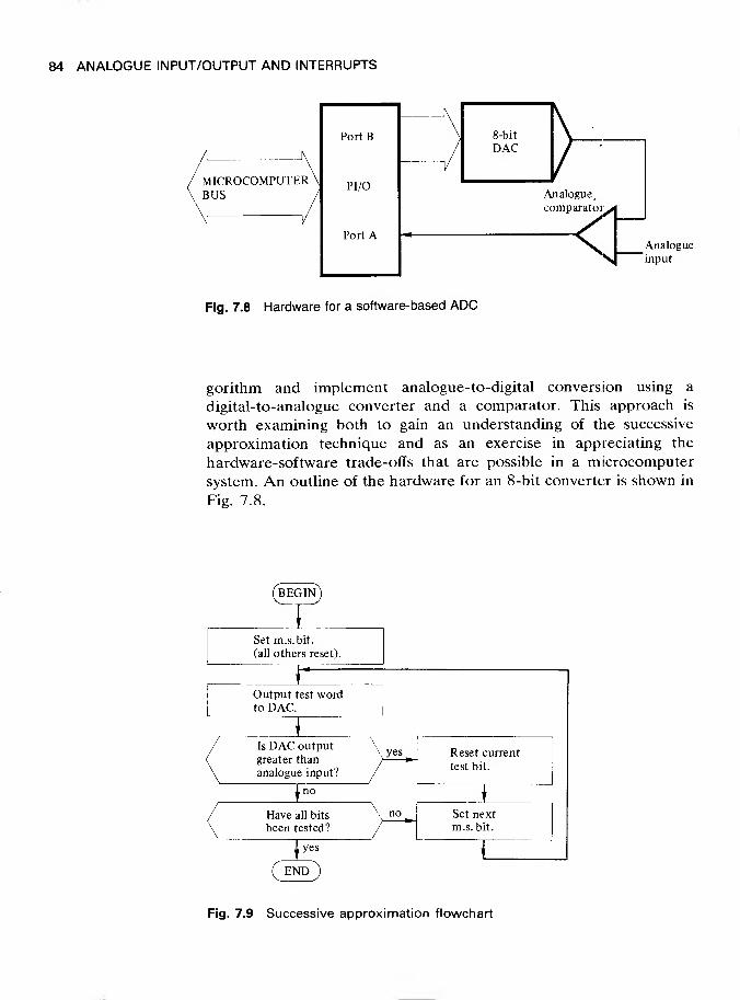
84 ANALOGUE INPUT/OUTPUT AND INTERRUPTS
MICROCOMPUTERBUS
Analogue
input
Fig. 7.8 Hardware for a software-based ADC
gorithm and implement analogue-to-digital conversion using a
digital-to-analogue converter and a comparator. This approach is
worth examining both to gain an understanding of the successive
approximation technique and as an exercise in appreciating the
hardware-software trade-offs that are possible in a microcomputer
system. An outline of the hardware for an 8-bit converter is shown in
Fig. 7.8.
(begin)
1
Set m.s.bit.
(all others reset).
1
Output test wordto DAC.
1'
yes_r Is DAC output
greater than
analogue input?
\Reset current
test bit.
\
no
'
no1
/ Have all bits
been tested? )Set next
m.s.bit.
1
yes*
END)
Fig. 7.9 Successive approximation flowchart

ANALOGUE INPUT/OUTPUT AND INTERRUPTS 85
Fig. 7.10 4-bit approximation sequence
Upward decision if DAC output not greater than input.
Downward decision if DAC output greater than input.
The algorithm consists essentially of setting first the most signific-
ant bit of the DAC input to 1 and then successive bits in order of
significance. At each step the comparator output is examined to see if
the resulting DAC output is greater than or less than the analogue
input. If it is greater, the current bit that is being tested is reset andthe next most significant bit tested. If it is less, the bit being tested is
held at 1 and the next bit is tested. The process repeats until all bits
have been tested. A flowchart for the algorithm is shown in Fig. 7.9
and the approximation sequence for a 4-bit converter is given in Fig.
7.10.
An alternative statement of the algorithm is given below simply to
illustrate a possible alternative representation of an algorithm.
Successive Approximation Algorithm
Start with m.s.b. of DAC set to 1, all other bits 0.
REPEATOutput DAC data.
Read comparator output.
IF DAC output is greater than analogue input
THEN reset current DAC test bit.
Set next most significant bit of DAC data.
UNTIL all DAC data bits have been tested.
Current DAC data is digital equivalent of analogue input voltage.

86 ANALOGUE INPUT/OUTPUT AND INTERRUPTS
Program Example 7.2: Analogue-to-Digital Conversion
The program of Fig. 7.11 implements the above successive approxi-
mation algorithm. It assumes that the 8-bit DAC is connected to port
B of a PI/O and the comparator output is connected to the m.s. bit
(bit 7) of port A. The comparator output is assumed high (logical 1) if
the DAC output is greater than the analogue input and low (logical
0) if it is less than the analogue input. The processor registers are
used as follows:
A is a working register
B contains the current DAC data
C contains the present test bit
D contains the bit count.
A number of additional devices are available which are frequently
used for interfacing analogue devices to a microcomputer. Three of
these devices are mentioned below.
1 Sample and hold circuits. These are used to sample a signal at a
precise time and hold the value constant during the conversion
process.
2 Analogue multiplexers. These devices permit one analogue
signal out of several to be selected by logical control signals.
3 Real-time clock. Signal sampling and construction is often
performed in conjunction with an interrupt driven real-time
clock. This device relieves the processor of the burden of
computing time delays.
7.4 Interrupts Typically the INput and OUTput instructions of a microprocessor
have an execution time of a few microseconds. In the majority of
applications, however, the controlled input and output devices
(peripherals) operate at a much slower rate: for example, a keypad
may be pressed once every few seconds, or a control valve maychange state, say, once every minute. It is potentially inappropriate
for the microprocessor to continuously monitor the state of the
control valve since the microprocessor might then spend most of the
time in a non-productive loop, waiting for a change of state to occur,
and hence no other processing could be carried out.
Whether or not this is a problem depends on the application; there
may be enough spare processor time to permit this inefficient use of
the microprocessor. If there is time available, repeatedly examining
an input looking for a change of status can be a simple procedure to
implement. If there is not adequate time available, a similar effect

ANALOGUE INPUT/OUTPUT AND INTERRUPTS 87
Assembly Instructions Comments
MVI A, 02 "I Initialise PI/0 — Port A input
OUT 20 J Port B output
MVI A, 80
MOV B, A Initialise DAC data.
MOV C, A Initialise DAC test bit.
MVI D, 08 Initialise bit count.
REPEAT: OUT 22 Output DAC data.
IN 21 Read comparator output.
ANA A Set flags.
JP COMZ Jump if comparator output zero.
XRA C Reset current DAC test bit.
COMZ: MOV B, A Save DAC data.
MOV A, C 1
RAR !> Update DAC test bit.
MOV C, A J
ORA B Set next m.s. bit of DAC data.
DCR D Decrement bit count.
JNZ REPEAT Jump if not zero.
Fig. 7.11 Program Example 7.2
can be obtained by causing the microprocessor to respond to the
status of a peripheral directly.
Most microprocessors provide a facility, called an interrupt, to
enable a peripheral device to inform the microprocessor when it
wishes to transfer data. Typically the microprocessor performs some
useful processing task until it receives an interrupt signal from the
peripheral device. On receipt of the interrupt, the microprocessor
temporarily suspends its current activity, performs the required input
or output operation, and then returns to its previous task. The

88 ANALOGUE INPUT/OUTPUT AND INTERRUPTS
Main Program Running
Interrupt
received
Time
Continue Main Program
t Return
from interrupt
Run Interrupt
Service Routine
Fig. 7.12 Interrupt service
program which performs this operation is known therefore as the
interrupt service routine and its activation is illustrated in Fig. 7.12.
In order to implement this scheme, on receipt of an interrupt the
microprocessor must perform a number of tasks:
1 Save the contents of the program counter - usually on the
system stack -so that it can return to the correct point in the
main program after the interrupt has been serviced.
2 Load the program counter with the start address (the memorylocation which holds the first instruction) of the interrupt ser-
vice routine.
3 Run the interrupt service routine.
Note: a) the first group of instructions in the routine usually
saves the current contents (again on the system stack) of those
processor registers which are used by the service routine itself.
This ensures that the action of the interrupted program is not
corrupted. Similarly at the end of the routine these contents are
restored.
b) after the appropriate processing the routine may, if this is
necessary, reset the interrupt, to indicate the interrupt has been
serviced.
4 Finally, return control to the interrupted program by restoring
the saved contents of the program counter from the system
stack.
7.4.1 Programming with Interrupts
An important consideration when writing a program which contains
an interrupt service routine is the frequency at which the interrupts
may be generated and the associated processing time required to
service each interrupt. The microprocessor is overloaded if the rate of

ANALOGUE INPUT/OUTPUT AND INTERRUPTS 89
generation of interrupts is such that there is insufficient time to
service them all. It is essential that the microprocessor has sufficient
time both to perform its main processing function and also to process
each interrupt.
Table Address +
+ 1
+ 99
Table Offset
'
Fig. 7.13 Circular buffer
To ensure that this is the case, it is necessary to estimate the actual
run time of each code segment - main program and interrupt service
routine(s) - by summing the individual instruction execution times in
each segment together. The manufacturer therefore provides the
execution time for each machine instruction. Typically, the number of
machine clock cycles required to execute each instruction is specified
by the manufacturer and hence, because the time for each cycle is
known - this is determined by the type of clock crystal being used - it
is an easy task to determine the execution time of each instruction.
As an example, consider an interrupt service routine which whenactivated reads a value from an input port and stores this in a table in
memory. Typically, the table may be organised as a circular buffer
which always contains the last, say, 100 values read from the port as
shown in Fig. 7.13. Assume that the main program continuously sumsthe values in the table together, computes the average (of the last 100
values), and outputs this value to an output port. A flowchart for the
complete program is therefore as shown in Fig. 7.14.

90 ANALOGUE INPUT/OUTPUT AND INTERRUPTS
Initialise
Segment
Main program<Segment
BEGIN
Initialise stack pointer.
Initialise Port A as an
input port and Port B as
an output port.
Clear Table contents to zero.
Reset vector interrupt mask.
Enable Interrupts.
Set table offset address to 0.
Set sum to zero.
Add next value in Table
to sum.
Increment offset by 1.
Does table offset - 100?
yes
Compute average value (sum/ 100)
and output to port B.
Interrupt
Service Routine^
Segment
BEGIN ISRJ
Save registers used in ISR on stack.
Read value from Port A and
store in Table.
Increment Table Pointer by 1.
Does Table Pointer - 100?
yes
Reset Table Pointer to
Restore registers from stack.
Return from interrupt.
Fig. 7.14 Interrupt service time example

ANALOGUE INPUT/OUTPUT AND INTERRUPTS 91
In this example, it is necessary to have sufficient time between
interrupts for both the main program to compute and update the
average value and also the interrupt service routine to enter each
value into the table. Thus if the maximum run time of the main
program is, say, 300 jjls and the interrupt service routine 200 jus, the
maximum rate which the above system could support is one interrupt
per 500 /xs. As the amount of processing time required in each
segment increases - especially if there is more than one interrupt
source - the corresponding rate at which interrupts can be serviced
will be reduced.
7.5 Multiple
Interrupts
The above scheme illustrates the actions which the microprocessor
must carry out on receipt of a single interrupt. In many applications,
however, the microprocessor may require to control a number of
input or output devices each with its own interrupt capability. The
Intel 8085, for example, is provided with five separate interrupt input
lines. When an interrupt is received, the microprocessor can automat-
ically determine from which device the interrupt has been sent since
it is caused to branch to a different fixed dedicated location in
memory for each of the five interrupt lines. These dedicated locations
are known as the vector addresses and for the Intel 8085 are as
shown in the table of Fig. 7.15.
Interrupt Input Vector Address
RST 4.5 (TRAP) 0024 (hex)
RST 5.5 002C
RST 6.5 0034
RST 7.5 003C
INTR The vector address for this input is
not fixed and is part of the instruction
placed on the data bus by the inter-
rupting device when the interrupt
request is acknowledged.
Fig. 7.15 8085 interrupt vector addresses

92 ANALOGUE INPUT/OUTPUT AND INTERRUPTS
Since each interrupt line may be connected to a different device, it
is clearly possible for these devices to generate interrupts simultane-
ously. In order to resolve simultaneous requests, the interrupt lines
have a priority associated with them:
RST 4.5
RST 7.5
RST 6.5
RST 5.5
(TRAP) Highest Priority
Lowest Priority
The TRAP interrupt has the highest priority and is always serviced
by the microprocessor immediately it is received. The three remain-
ing interrupts, however, are serviced only when the microprocessor is
ready to do so. There are two machine instructions:
EI (Enable Interrupts)
and
DI (Disable Interrupts)
which can be used by the programmer to determine when interrupts
should be recognised and therefore serviced. Even though interrupts
may be enabled, it is additionally possible for the programmer to
individually mask each of these interrupts and therefore prevent
them from interrupting the processor. This is used, for example, if it
is necessary to ensure that an interrupt is serviced completely before
allowing another interrupt to be recognised. The interrupt enable flag
is reset after the recognition by the processor of a valid interrupt.
m.s l.s.
I
EM7.5
M6.5
M5.5
Interrupt Masks
• Interrupt Enable Flag
Mask Bit = 1 Disable corresponding interrupt= Enable corresponding interrupt
Fig. 7.16 IM-register format
The status of the interrupt enable flag and the three mask bits is
held in the IM-register of the processor and its format is shown in
Fig. 7.16.
ANALOGUE INPUT/OUTPUT AND INTERRUPTS 93
The three mask bits may be set or reset by means of the SIMinstruction:
SIM (Set Interrupt Mask)
The A-register is first loaded with the required mask bits in the three
least significant bit positions together with a logical 1 in the fourth bit
(mask set enable) and the SIM instruction is then given. For example,
MVI A, 08
SIM
will result in all the mask bits being reset and therefore enabling the
three interrupt lines.
Similarly, the status of the mask bits may be examined by means of
the RIM instruction
RIM (Read Interrupt Mask)
After a RIM instruction, the least significant three bits of the A-register indicate the state of the corresponding mask bit.
7.5.1 Interrupt Priority Levels
Since the microprocessor can only service one interrupt at a time, it is
necessary for the programmer, when writing each interrupt, to decide
the relative priority of each interrupt and hence controlled device.
For instance, an interrupt indicating an alarm condition should have a
higher priority and hence precedence over the service of an interrupt
from a device operating normally.
To illustrate the use of priority assignment of different interrupt
inputs, assume the following assignment scheme:
Priority
TRAP power failure HIRST 7.5 over-temperature alarm
RST 6.5 real-time clock > '
RST 5.5 read new temperature set LOvalue
In the Intel 8085 the TRAP interrupt has the highest priority and is
non-maskable. This means that it will always be recognised im-
mediately it occurs and is therefore best reserved for catastrophic
alarm conditions such as power failure as indicated above. The three
other interrupts, RST 7.5, 6.5 and 5.5, may typically be assigned in
the order indicated above. This assignment will mean that, if the
three interrupts occur simultaneously, the first to be serviced will be
the over-temperature alarm, the second the real-time clock (this is
discussed in detail in Chaper 8), and finally the read new set value.
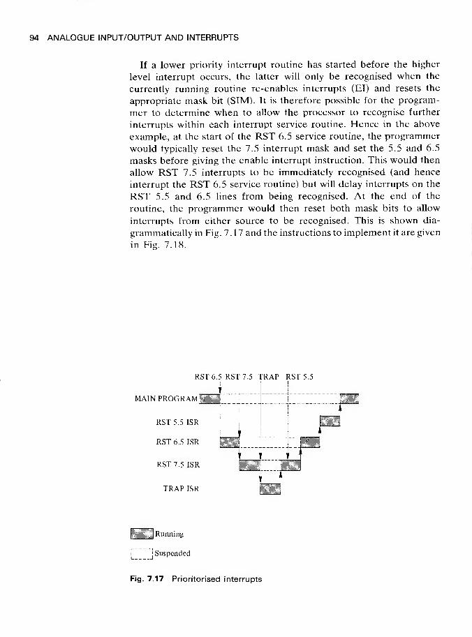
94 ANALOGUE INPUT/OUTPUT AND INTERRUPTS
If a lower priority interrupt routine has started before the higher
level interrupt occurs, the latter will only be recognised when the
currently running routine re-enables interrupts (EI) and resets the
appropriate mask bit (SIM). It is therefore possible for the program-
mer to determine when to allow the processor to recognise further
interrupts within each interrupt service routine. Hence in the above
example, at the start of the RST 6.5 service routine, the programmer
would typically reset the 7.5 interrupt mask and set the 5.5 and 6.5
masks before giving the enable interrupt instruction. This would then
allow RST 7.5 interrupts to be immediately recognised (and hence
interrupt the RST 6.5 service routine) but will delay interrupts on the
RST 5.5 and 6.5 lines from being recognised. At the end of the
routine, the programmer would then reset both mask bits to allow
interrupts from either source to be recognised. This is shown dia-
grammatically in Fig. 7.17 and the instructions to implement it are given
in Fie. 7.18.
RST 6.5 RST 7.5 TRAP RST 5.5
i.MAIN PROGRAM
TRAP ISR
Running
i ' Suspended
Fig. 7.17 Prioritorised interrupts

Assembly Instructions Comments
MainProgram /
BEGIN: MVI A, 08
SIM
EI
5.5 Interrupt
Service Routine^
ISR5.5: PUSH PSW
MVI A, 09
SIM
EI
6.5 Interrupt
Service Routine
RET
ISR6.5: PUSH PSW
MVI A, OB
SIM
EI
7.5 Interrupt
Service Routine <(
RET
ISR7.5: PUSH PSW
MVI A, OF
SIM
EI
RET
Reset all mask bits
and enable interrupts
Disable 5.5 interrupts
}>and enable 6.5 and 7.5
interrupts
Disable 5.5 and 6.5
^interrupts and
enable 7.5 interrupts
>;Disable 5.5, 6.5 and 7.5
interrupts
Fig. 7.18 Priority interrupts example
95
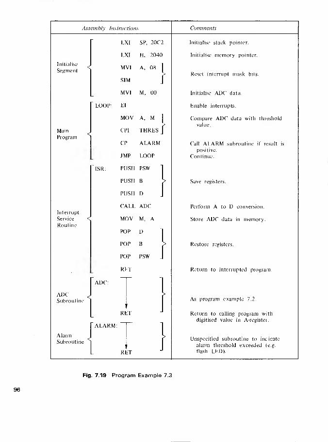
Assembly Instructions Comments
LXI SP, 20C2 Initialise stack pointer.
LXI H, 2040 Initialise memory pointer.
Initialise
SegmentMVI
SIM
A, 08 1
Reset interrupt mask bits.
MVI M, 00 Initialise ADC data.
" LOOP: EI Enable interrupts.
Main
Program
MOV
CPI
A, M 1
THRES J
Compare ADC data with threshold
value.
CP ALARM Call ALARM subroutine if result is
JMP LOOPpositive.
Continue.
~ISR: PUSH PSW
PUSH B > Save registers.
PUSH D
Interrupt
Service <
Routine
CALL
MOV
POP
ADC
M, A
D1
Perform A to D conversion.
Store ADC data in memory.
POP B Restore registers.
POP PSW J
RET Return to interrupted program.
ADC:1
ADC <Subroutine
' '
1
>As program example 7.2.
RET -Return to calling program with
digitised value in A-register.
ALARM:1
AlarmSubroutine
RII
Unspecified subroutine to indicate
alarm threshold exceeded (e.g.
flash LED).
Fig. 7.19 Program Example 7.3
96

ANALOGUE INPUT/OUTPUT AND INTERRUPTS 97
Program Example 7.3: Interrupts
The program example of Fig. 7.19 is intended to illustrate the use of
a microprocessor with an interrupt. The program first initialises anarea of memory as a stack and resets the interrupt mask bits. It then
continuously compares the data returned by subroutine ADC -forexample the successive approximate program of example 7.2 -with a
preset threshold value (THRES). If this value is equalled or ex-
ceeded, subroutine ALARM is called which is assumed, in someunspecified way, to indicate that this condition exists. Analogue-to-
digital conversion is performed on receipt of an interrupt on the RST7.5 interrupt line. The instruction JMP ISR must therefore be stored
in memory starting at the interrupt vector address 003C(hex).
Exercises
7.1 Modify the assembly language program of example 7.1 to produce a triangular
waveform, both positive and negative ramps.
7.2 Modify program example 7.1 to make the ramp rate selectable by a digital
value read from a set of eight switches connected to port A of the PI/O.
7.3 Assuming an average instruction execution time of 3.0 /as determine the
conversion time of the 8-bit ADC program listed in program example 7.2.
7.4 Modify program example 7.3 so that a LED indicator connected to a PI/O will
alternately turn on and then off when the threshold value has been exceeded.

8 Application Examples
8.1 Introduction This chapter is intended to demonstrate how a microprocessor, with
the aid of a number of additional peripheral devices, may be used in
a variety of different applications. These applications are dealt with in
a simplified way to present application programming techniques in as
direct a way as possible. The first two examples are concerned with
sequence controllers. The third example is a digital clock for which
the microprocessor performs the complete timing sequence and
drives a numeric display directly with simple digital outputs. The use
of a digital-to-analogue converter is demonstrated in the fourth
example which illustrates the use of a microprocessor to generate
waveforms typical of those used in many electronic systems. The final
example uses an analogue-to-digital converter to monitor the output
of a temperature transducer in a microprocessor-based temperature
controller.
8.2 Basic
SequencingChapter 6 introduced the instructions provided by a microprocessor
to input and output logical data to or from an external device and
also showed how a programmable input/output (PI/O) port may be
used to provide the necessary latching and isolation functions.
In many industrial applications a logical input may be derived from
a thermostat, for example, indicating whether or not a certain temp-
erature has been reached, or perhaps a function selection switch on
the equipment front panel indicating that a certain mode of operation
is required. Similarly, logical outputs may be used to activate a relay
which in turn controls the state - ON or OFF - of a pump or heater
for example.
To illustrate a simple application of this type, which uses only
logical outputs, consider a basic sequencer. Typically, a sequencer
98

APPLICATION EXAMPLES 99
activates a number of devices in a preset sequence with a preset time
delay between each new device state. For example, a traffic light
sequencer changes the state of each light in a set of traffic lights in a
preset sequence with a time delay between each state.
A microprocessor is used as a basic sequence controller by switch-
ing the appropriate logical output lines on or off - logical 1 or - in
the specified sequence with the required time delay between changes
computed by the microprocessor.
8.2.1 A Traffic Light Sequencer
As an example of a basic sequencer consider the sequencing of a set of
traffic lights. The U.K. sequence is: red; red and amber together;
green; amber; red again; etc. The controlled road junction is shownin Fig. 8.1. It comprises the four roads labelled North, South, East
and West and a set of traffic lights at each corner (RAG).
West-
North
South
East
R = RedA = AmberG = Green
Fig. 8.1 Controlled road junction
The two sets of lights seen by traffic approaching the junction from
North and South change in the same sequence. Similarly, the two sets
seen by traffic approaching from East and West also change in the
same sequence.
The sequence the controller must implement is shown in Fig. 8.2.
Note that two different delay times are used during the complete
cycle.

100 APPLICATION EXAMPLES
Program Example 8.1: Traffic Light Sequence
The sequence of Fig. 8.2 is presented in a computer-compatible form
by the state table given in Table 8.1. Note that two flag bits have
been used to indicate if the delay following the respective state is
delay 1 (Dl) or delay 2 (D2). (Only one flag is strictly necessary.) In
the table a 1 indicates the corresponding light should be ON and a
indicates the light should be OFF.
North/South East/West
Red Amber Green Red Amber Green
ON OFF OFF OFF OFF ONdelay 1 L
ON OFF OFF OFF ON OFFdelay 2 (
ON OFF OFF ON OFF OFFdelay 2 t
ON ON OFF ON OFF OFFdelay 2 [
OFF OFF ON ON OFF OFFdelay 1 L
OFF ON OFF ON OFF OFFdelay 2 L
ON OFF OFF ON OFF OFFdelay 2 i
ON OFF OFF ON ON OFF
Fig. 8.2 Traffic light sequence
Delay 1 = long delay between overall direction changes (~2 mins)
Delay 2 = short delay between transitional light settings (~3 sees)
Table 8.1 Traffic light state table
N/S E/W DelayState
R A G R' A G' D1 D2
1 1 1
1 1 1 1
2 1 1 1
3 1 1 1 1
4 1 1 1
5 1 1 1
6 1 1 1
7 1 1 1 1

APPLICATION EXAMPLES 101
The sequencer can be implemented by storing this state table in
memory and stepping through it. The appropriate states of the lights
are then output, writing the appropriate delay time between steps.
This is shown in the flowchart of Fig. 8.3. This flowchart assumesthat the most significant three bits of port A of an Intel 8155 PI/Odevice drive the North/South lights (RAG) and the next most signific-
ant three bits drive the East/West lights (R'A'G').
The delay times are implemented in two stages. With each newstate, a delay of D2 is executed and then, if required, a further delayof D1-D2 is executed. (A program implementing this is given in Fig.
8.4.)
(begin)
'
Initialise stack pointer.
Initialise port A as
output.
'
Initialise pointer
to start of state table.
_'
yesm
/ Output new state. /
\
Delay time 2
(short delay).
<
'
\Delay time 1
required?Delay time 1
.
no,« i
1
Increment memorypointer to next
state address.
no/'
>End of table?\
'yes
Fig. 8.3 Flowchart for traffic light sequence

Assembly Instructions
SEQ:
NEWSTATE:
NEXT:
DELAY 1:
DELAY2:
LXI SP, 20C2
MVI A, 01
OUT 20
LXI H, 2080
MOV A, M
OUT 21
CALL DELAY2
ANI 02
JZ NEXT
CALL DELAY 1
INX H
MOV A, L
CPI 88
JNZ NEWSTATE
JMP SEQ
RET
RET
}
Comments
\
2080: 86
2081: 89
2082: 91
2083: Dl
2084: 32
2085: 51
2086: 91
2087: 99
Initialise stack pointer.
Initialise port A as output.
Initialise memory pointer to start
of state table.
Update state.
Short delay subroutine.
Is Dl required?
No: skip Dl call.
Yes: call long delay subroutine.
Update memory pointer.
End of table?
No: loop for next state.
Yes: loop to start of table.
Delay subroutines similar to
those of Program Example 5.3
Table of light states.
Fig. 8.4 Program Example 8.1
102

APPLICATION EXAMPLES 103
8.3 Conditional
SequencingIn some sequencing applications, instead of a change of state occur-
ring after a preset delay, a change of state may be dependent on the
occurrence of an external event: for example, water in a vessel
reaching a certain level or temperature. This is often referred to as
conditional sequencing. The state of an external device can be readily
monitored by a microprocessor simply by looping within the program
on a particular logical input line waiting for the required change to
occur. It is thus possible to use a microprocessor to implement a
conditional sequence controller. As an example in the next section a
simplified washing machine controller is considered.
8.3.1 A Washing Machine Controller
A washing machine controller is a conditional sequencer which
involves both external condition inputs and internal preset time de-
lays. The principles encompassed by this example are applicable to
many industrial sequencer applications. The controlled devices inter-
faced to the logical outputs and the input condition signals for a
simplified controller are shown in Table 8.2. A typical sequence of
actions for the controller is therefore as given in Table 8.3. This
sequence can be directly translated into the state table of Table 8.4.
This table is arranged such that the next entry in the table after a
state with no time delay is the necessary input condition information.
Table 8.2 Controlled devices and logical inputs for
washing machine
Logical outputs
1
2
3
4
5
Logical inputs
1
2
Controlled device
Hot water control valve
Cold water control valve
Water heater
Tub motor -wash/rinse speedPump motor (for emptying tub)
Tub motor -spin speed.
Significance
Tub full
Water thermostat

104 APPLICATION EXAMPLES
Table 8.3 'Simplified washing machine sequence
State Controlled device
number 1 2 3 4 5 Action
"0 ON OFF OFF OFF OFF OFF Fill tub with hot water
until full.
1 OFF OFF ON OFF OFF OFF Heat water until
WASH thermostat closes.
2 OFF OFF OFF ON OFF OFF Rotate tub at wash/rinse
speed for a fixed time D1.
i-3 OFF OFF OFF OFF ON OFF Empty tub for a fixed
time D2.
-4 OFF ON OFF OFF OFF OFF Fill tub with cold v»ater
RINSE until full.
5 OFF OFF OFF ON OFF OFF Rotate tub at wash/rinse
speed for fixed time D1.
L6 OFF OFF OFF OFF ON OFF Empty tub for a fixed
time D2.
SPIN 7 OFF OFF OFF OFF OFF ON Spin for fixed time D1.
OFF OFF OFF OFF OFF OFF OFF Stop
Table 8.4 Washing machine controller state table
State Controlled device Delay/Input
number 12 3 4 5 D1/1 D2/2
101 tub full
1 101 1 thermostat
2 10 1
3 10 1
4 101 tub full
5 10 1
6 10 1
7 1 1
8 1

APPLICATION EXAMPLES 105
Program Example 8.2: Washing Machine Controller
The controller program must simply step through each state of Table8.4 and implement the appropriate delay or loop for the relevant
condition input. This table approach makes it easy to extend to larger
numbers of states and controlled devices.
A flowchart for the controller is given in Fig. 8.5. The logical
outputs are assumed to be six bits of port A and the two inputs are
connected to port B of a PI/O device as illustrated in Fig. 8.6.
(begin)
'
Initialise stack pointer.
Initialise PI/O ports.
Initialise pointer to
start of state table.
'
/ Output new /
/ state. /
'
/ Is time
\ requir
, delay \ yes
5dV'
no
no
' ( Dl? ~>
/ Read input // conditions. /
lyes'
WaitDl |
i
Wait D2
t
>
'
/ Has required condition \\ been satisfied? /
yes '
Increment memorypointer to next state
address.
t
r / PnH nf table ? \
'
yes
(end)
Fig. 8.5 Flowchart for Program Example 8.2

106 APPLICATION EXAMPLES
A program corresponding to the flowchart of Fig. 8.5 is presented
in Fig. 8.7. The program terminates with a HALT instruction;
restarting the program is achieved by a processor RESET with a JMPSTART instruction at the RESET vector memory address
(OOOO(hex)). RESET is a processor input that causes a response
rather like an enabled RST input, except that various processor
control functions are reset. It is primarily used to establish the
processor in a known condition after the application of power.
Microprocessor
bus
Port A
PI/O
PortB
m i
Hot water control valve
Cold water control valve
Water heater
Tub motor (wash/rinse speed)
Pump motor
Tub motor (Spin speed)
Water level
Thermostat
Fig. 8.6 PI/O signals for washing machine controller
8.4 Digital Clock Many microprocessor applications are concerned with performing
specific control functions or actions at preset times throughout the
day. For example, an irrigation control system may require a water
supply to be turned on at specific intervals, a domestic central heating
controller may require a boiler to be switched on at preset times, and
so on. A basic requirement for this type of application, therefore, is a
real-time digital clock often with a displayed output of the current
time.
The delay subroutine described earlier in Chapter 5 demonstrated
how a short time delay can be generated with software by executing a
number of instructions repetitively in a loop. Although this is a
convenient method for generating a single delay, an alternative and
better method for generating a continuous timing function is to use

Assembly Instructions Comments
START: LXI SP, 20C2 Initialise stack pointer.
MVI A, 01 1Initialise port A to be output and port B
OUT 20 Jto be input.
LXI H, 2080Initialise memory pointer to start of state
table.
NEWSTATE: MOV AM 1
Output newstate.
OUT 21 J
ANI 03 Is delay required?
JZ COND No: skip to conditional section.
ANI 02 1
Yes: is it D 1?
JZ D2J
CALL DELAY
1
Yes: compute Dl.
JMP INCM Skip conditional section.
D2: CALL DELAY2 No: then D2.
JMP INCM Skip conditional section.
COND: INX H Increment state table pointer.
CONDI: IN 22 Read conditions.
SUB M Test conditions.
JNZ CONDI Loop until conditions are met.
INCM: INX H Point to next state.
MOV A, L 1
End of sequence'.'
CPI 8CJ
JNZ NEWSTATE No: loop for next state.
DELAY1:
HALT
I
Yes: finish.
Subroutine implementing program delay|T
RET r time Dl.
DELAY2:! l Subroutine implementing delay time
RET fD2.
Fig. 8.7 Program Example 8.2
107

108 APPLICATION EXAMPLES
an additional hardware device called a programmable timer. These
are now available from most microprocessor manufacturers either as
separate devices or combined with other memory and input/output
circuits. The Intel 8155, for example, is a single integrated circuit
which incorporates a programmable timer with a 256x8 bit static
RAM and three programmable input/output ports.
The programmable timer within the Intel 8155 is typical of these
devices. It consists of a 14-bit counter which may be programmed to
generate either a square wave of a selectable period or a terminal
count pulse. The counter operates in the binary count down modeand counts the "timer input" pulses. The initial count length is
programmable and when the count becomes zero a pulse is generated
on the "timer output" line.
The timer input is normally driven from the microprocessor gener-
ated clock and hence, if this has a period of, say, 0.5 /xs, the time
interval may be varied up to a maximum of
(214 - 1) x 0.5 ills that is, Tmax^8.1915 ms
The timer may be programmed either to stop after the terminal count
pulse is generated or to continue counting and hence generate a newcount pulse every, say, 8.1915 ms.
Since the microprocessor clock is normally quite stable, a conve-
nient method of producing a digital clock is to use the programmable
timer to continuously generate a count pulse every, say, 5 ms and to
connect the timer output to one of the interrupt input lines (RST 7.5)
of the microprocessor. The interrupt service routine must then count
the interrupts and convert these first into seconds (after 200 inter-
rupts) and then into minutes and hours. A suitable flowchart for such
a routine is shown in Fig. 8.8.
The routine uses the following symbolic names which correspond
to successive locations in RAM:
COUNT contains the current number of interrupts since the last
change in SECS.
SECS contains the two BCD digits corresponding to seconds.
The contents are incremented by 1 each time COUNTreaches 200.
MINS contains the two BCD digits corresponding to minutes.
The contents are incremented by 1 each time SECSreaches 60.
HOURS contains the two BCD digits corresponding to hours.
The contents are incremented by 1 each time MINSreaches 60.

APPLICATION EXAMPLES 109
(™D
Add 1 to COUNT
Is COUNT 200?
IS SECS = 60?
yes
Reset SECS to
Add 1 to MINS and
adjust for decimal.
IS MINS = 60?
yes
Reset MINS to 0.
Add 1 to HOURS and
adjust for decimal.
'
yes
Reset COUNT to 0.
Add 1 to SECS and
adjust for decimal.
'
IS HOURS = 24?
yes
Reset HOURS to 0.
(^RET
Fig. 8.8 Interrupt service routine

110 APPLICATION EXAMPLES
To display the current time in hours and minutes it is possible to use
the two 8-bit ports of the 8155 to drive four BCD-to-seven-segment
decoder drivers directly. Again these circuits are readily available
from a number of manufacturers and can be used to drive a seven-
segment LED display. The latter uses an array of seven light emitting
diodes (LEDs) to display each decimal digit. The arrangement is
shown in Fig. 8.9.
-
—BCD to
^
BCD digit—*~
from8155 ~~**
seven-segment
decoder
driver
-
^* ""
Seven-segment
LED display
Fig. 8.9 Seven-segment display and driver
Program Example 8.3: Digital Clock
A program for the clock system can now be written. The program is
made up of three parts: an initialisation segment, the main program,
and an interrupt service routine.
The initialisation segment is run when the system is first switched
on. It initialises the stack pointer and clears the various memorylocations used for COUNT, SECS and MINS to zero. HOURS is
preset to 12; this gives a simple means of starting the clock after
switching on with the clock programmed to start at noon. (Any
current time could be preset into these locations by means of a
keypad and a short program.) Ports A and B are then initialised as
outputs (the timer mode is selected for continuous operation) and the
timer count length is loaded to produce 5 ms interrupts. Interrupts
are then enabled and the program is run.
The main program simply outputs the current time in hours and
minutes via ports A and B, but clearly additional control functions
could be included if the clock were only one component of a
controlled system.
Finally, the interrupt service routine implements the flowchart
shown in Fig. 8.8 and simply updates the current time on receipt of
each interrupt. The following addresses are used in the program:

APPLICATION EXAMPLES 111
Intel
8085
RST7.5
HOURS MINS
I
Address busJOT
D uPort A
rrrr mr tttt TinPortB
256x8RAM Timer
37
Data bus
Clock output
Interrupt input
Fig. 8.10 Digital clock schematic
RAM addresses:
2QC2 stack pointer
2080 COUNT2081 SECS2082 MINS2083 HOURS
8155 addresses:
Command Register 20 (hex)
Port A data 21
Port B data 22
Low order byte of count length 24
High order byte of count length 25
The program may be stored in any area of memory but an interrupt
vector instruction (JMP ISR) must be stored in the vector address
corresponding to the interrupt line used by the timer. After the
microprocessor is reset, it starts program execution at location 0000.
The instruction at this address should therefore be a jump to the start
of the initialisation segment. The complete program is given in Fig.
8.11. In any application using interrupts it is important to ensure that
interrupts can be serviced at least as quickly as they can be gener-
ated. For the clock this means that the interrupt service routine, ISR,
must take less than 5 ms to be executed.

112 APPLICATION EXAMPLES
Fig. 8.11 Digital clock program
Assembly Instructions Comments
LXI SP, 20C2 Initialise stack pointer.
LXI H, 2080
MVI M, 00
INX H
MVI M, 00
>Clear COUNT, SECS and MINS
to zero.
INX H
MVI M, 00
Initialise
Segment
INX H 1
MVI M, 12 J
MVI A, 10 "1
Preset HOURS to 12.
OUT 24 1Initialise count length for 5ms
interrupts (0.5 jus clock).
MVI A, 27
OUT 25 J
MVI A, C3 1
OUT 20 J
Initialise ports A and B as output
and timer for continuous operation.
MVI A, 08 1
SIM J
Reset interrupt mask bits.
"LOOP: EI Enable interrupts.
LXI H, 2082 1
MOV A, M >Load minutes digits into A and
output to port B
MainProgram
OUT 22 J
INX H 1
MOV A, M >Load hours digits into A and
output to port A
OUT 21 J
JMP LOOP
ISR: PUSH PSW 1
PUSH H J
Save register contents.
LXI H, 2080 1 Add 1 to COUNT
INR M J

MVI A, C8 1 Is COUNT = 200?
CMP M S
JNZ END J No: END
MVI M, 00 Yes: reset COUNT to zero.
INX H
MOV A, M
INR A >Add 1 to SECS and adjust,
for decimal.
DAA
MOV M, A
MVI A, 60 "I
Is SECS = 60?
CMP M J
JNZ END No: END
MVI M, 00 Yes: reset SECS to zero.
Interrupt INX HService <
Routine MOV A, M
INR A >Add 1 to MINS and adjust
for decimal.
DAA
MOV M, A
MVI A, 60 "I
Is MINS = 60?CMP M J
JNZ END No: END
MVI M, 00 Yes: reset MINS to zero.
INX H
MOV A, M
INR A >Add 1 to HOURS and adjust
for decimal.
DAA
MOV M, A
MVI A, 24 1Is HOURS = 24?
CMP MJ
JNZ END No: END
MVI M, 00 Yes: reset HOURS to zero.
END: POP"
1 Restore register contents.
POP PSW J
RET Return from interrupt.
113

114 APPLICATION EXAMPLES
8.5 Waveform The following example has been chosen to demonstrate, firstly, the
Generation use of a DAC to convert the digital outputs from a microprocessor
into an analogue form and, secondly, to illustrate the use of a look-up
table. The latter is used in many microprocessor applications and, in
conjunction with the piecewise linearisation algorithm also described,
is a particularly useful technique.
The generation of a repetitive sawtooth waveform using a simple
binary counter and a DAC was described in Program Example 7.1.
The A-register within the microprocessor was used as a counter and
its contents were incremented by unity within a program loop. The
contents were output to the DAC after each count increment.
Alternative waveforms may be readily produced by using the
contents of the counter, not to drive the DAC directly but instead to
provide addresses to successive memory locations, the contents of
which store the required digital value which is to be output to the
DAC. The contents of the block of successive memory locations used
in this way are often referred to as a table and this procedure as a
table loop-up process. This is illustrated in Fig. 8.12.
To illustrate the above process, consider the generation of a
sinewave. Since the A-register contains 8 bits there are 28or 256
count states. Similarly, assume that the DAC also has 8 bits, and
consequently the 8-bit digitised values corresponding to each of the
256 count states are first determined and stored in a table comprising
256 successive locations in memory as indicated in Fig. 8.13.
A repetitive sinewave can then be generated by simply increment-
ing the contents of the A-register by unity in a program loop, and
using the contents as an offset address to find the corresponding
digitised value in the table, which is then output to the DAC.
Program Example 8.4: Waveform Generation
The following program example generates a repetitive sinewave using
a table look-up process. The table is stored in memory starting at
address 2000 and register pair HL is initialised to this value. Register
L is then used as the 8-bit counter and the combined contents of
register pair HL therefore provides the complete 16-bit memoryaddress automatically. Moreover, on reaching FF, the contents of
register L will return to 00 and hence the combined contents of HLwill return to 2000 and the process will repeat. See Fig. 8.14 for
program.
It is clearly possible to extend the size of the table should greater
resolution be required and use, for example, a combined register pair
as a counter. For many applications, however, it is possible to reduce
the number of look-up values (and hence the size of the table) by
using piecewise linear interpolation.

APPLICATION EXAMPLES 115
Binary
CounterAddress
Table of
Digitised
Values
Contents DACAnalogue
Output
Fig. 8.12 Waveform generation
Count
127-
256 count states
255
Fig. 8.13 Sinewave table generation
Assembly Instructions Comments
MVI A, 01 1
OUT 20 J
Initialise port A as an output port.
LXI H, 2000
LOOP: MOV A, M
Initialise register pair HL to point to
start of table.
Look up value from table.
OUT 21 Output value to DAC.
INR L Increment table offset.
JMP LOOP
Fig. 8.14 Waveform generation by table look-up
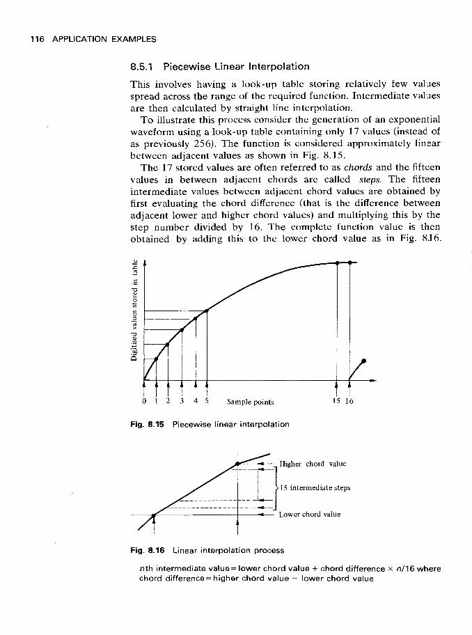
116 APPLICATION EXAMPLES
8.5.1 Piecewise Linear Interpolation
This involves having a look-up table storing relatively few values
spread across the range of the required function. Intermediate values
are then calculated by straight line interpolation.
To illustrate this process consider the generation of an exponential
waveform using a look-up table containing only 17 values (instead of
as previously 256). The function is considered approximately linear
between adjacent values as shown in Fig. 8.15.
The 17 stored values are often referred to as chords and the fifteen
values in between adjacent chords are called steps. The fifteen
intermediate values between adjacent chord values are obtained by
first evaluating the chord difference (that is the difference between
adjacent lower and higher chord values) and multiplying this by the
step number divided by 16. The complete function value is then
obtained by adding this to the lower chord value as in Fig. 816.
Sample points
Fig. 8.15 Piecewise linear interpolation
-f— Higher chord value
>15 intermediate steps
Lower chord value
Fig. 8.16 Linear interpolation process
nth intermediate value = lower chord value + chord difference x n/16 wherechord difference = higher chord value - lower chord value

APPLICATION EXAMPLES 117
Program Example 8.5: Piecewise Linear Interpolation
The following program generates an exponential waveform using a
table look-up process and piecewise linear interpolation as outlined
above. The program does not actually perform multiplication to formeach intermediate value, but instead maintains a current increment
value (chord difference x n) and simply adds the chord difference to
this following each iteration.
In order to maintain accuracy, the current increment value is held
as a 16-bit number in register pair BC and the combined contents are
divided by 16 to form each intermediate value. This is accomplished
in principle by shifting the current increment value four places to the
right but, since no shift instructions are available with register pairs,
this process is performed in a separate subroutine.
The current increment value is passed to the subroutine in register
pair BC and the 8-bit result of the division operation is returned in
register A.
Thus, if (B) = OX (hex) (m.s. 4 bits of B are always zero)
(C) = YZ (hex)
then (A) <- result = XYA flowchart for the subroutine is shown in Fig. 8.17 and the
corresponding program is given in Fig. 8.18.
A flowchart for the complete program using this subroutine is
shown in Fig. 8.19. The corresponding program for the flowchart of
Fig. 8.19 is given in Fig. 8.20. The register usage is:
HL = Table Address (initialised to 2080 hex)
SP = Stack Pointer (initialised to 20C2 hex)
BC = Current Increment Value
D = Chord Difference
E = Step Count
0>>
1
Shift (B) 4 places left i.e. (B) — X0
Mask off lower 4 bits of (C) i.e. (C) — Y0
Shift (C) 4 places right i.e. (C) — 0Y
Logical OR (B) and (C) together i.e. (A)— XY
I(^"reF)
Fig. 8.17 Flowchart for divide-by-16 subroutine

118 APPLICATION EXAMPLES
Assembly Instructions Comments
DIV: PUSH B Save Current Increment Value on stack.
MOV A, B (B) = OX
RLC
RLC
RLC > Rotate B 4 places left i.e. (B) = XO
RLC
MOV B, A
MOV A, C (C) = YZ
ANI FO
RRC >Mask off l.s. 4 bits of C and rotate
4 places right.
RRC
RRC (A) = OY
RRC (A) = (A) OR (B) = XY
ORA B Restore Current Increment Value from stack.
POP B
RET
Fig. 8.18 Program corresponding to Fig. 8.17

APPLICATION EXAMPLES 119
(begin)
Initialise Table Offset to zero
Set Current Increment Value to zero.
Read Lower and Higher Chord Values from table.
Compute Chord Difference.
Initialise Step Count to 15.
Add Chord Difference to TemporaryIncrement Value.
Divide result by 1 6 (subroutine DIV)and add to Lower Chord Value.
Output result to DAC.
Decrement Step Count.
Is Step Count = 0?
yes
Increment Table Offset
Is Offset = 16?
yes
Fig. 8.19 Flowchart for Program Example 8.5

Assembly Instructions Comments
LXI SP, 20C2 Initialise stack pointer.
MVI
OUT
A, 01 1
20 J
Initialise port A as an output port.
START: LXI H, 2080 Initialise HL to start of Table.
LXI B, 0000 Clear BC.
CONT: INR
MOV
1
}A, M J
Obtain Higher Chord Value from Table.
DCRl
SUB M \ Subtract Lower Chord Value to form
Chord Difference and save in D.
MOV DA J
MVI E, OF Set Step Count to 15.
STEP: MOV
ADD
A, C
D
MOV C, A >Add Chord Difference to 16-bit
Current Increment Value.
JNC NOC
INR B
NOC: CALL
ADD
DIV 1
M J
Divide Current Increment Value by16 and add to Lower Chord Value.
OUT 21 Output value to DAC.
DCR
JNZ1
STEP J
Test if Step Count :=
INR L 1
MOV A, LJ>
Increment Table Offset andtest if = 16.
CPI J
JNZ CONT No — continue
JMP START Yes — reinitialise Table Offset and
repeat.
120
Fig. 8.20 Program Example 8.5

APPLICATION EXAMPLES 121
8.6 TemperatureController
This application example is intended to demonstrate how a micro-
processor, with the addition of an analogue-to-digital converter
(ADC), can be used as a process controller. A temperature control
system has been selected but the principles are applicable to manydifferent processes. A simple ON/OFF control philosophy is used
although it is possible to extend this to a more sophisticated propor-
tional or proportional plus integral control algorithm.
The required temperature Tref is assumed to be variable and is
stored in a location in RAM. Similarly, the tolerance limits on the
required temperature, ±AT, are also assumed variable and stored in a
second RAM location. A schematic diagram of the control system is
shown in Fig. 8.21.
The controlled temperature is monitored by first deriving an
analogue voltage proportional to the temperature - from a thermistor
and associated amplifier, for example - and then converting this vol-
tage into an 8-bit digital value by means of an ADC.The supply to the heater is controlled by a single digital output
from the microprocessor via a suitable driver and relay: a logical 1
switches the heater on, a logical switches the heater off. Thus, if the
input temperature Tin is greater than (Tre/+AT) the heater is turned
off, whilst if the input temperature is less than (Tref-AT) the heater is
turned on. This control action is summarised in the flowchart of Fig.
8.22.
\//M/M/////M>/m
<s:Temperaturesensor
Heater 'jA Controlled
^\/\/\l\p—. ^ environment
Power supply
I
Amplifier
Tin
ADC
Start
conversion
Driver
andRelay
7
PORTA
Microprocessor
PORTB
Controller
Fig. 8.21 Temperature control system

122 APPLICATION EXAMPLES
(begin)
Start conversion and
wait convert time.
Read digitised input
temperature from ADC.
Tin <(Tref + *D?
yes
Switch heater ON. Tin >(Tref + AT)l
yes
Switch heater OFF.
Fig. 8.22 Temperature controller flowchart
Program Example 8.5: Temperature Controller
The program given in Fig. 8.23 implements the flowchart of Fig.
8.22. The required temperature Tref is assumed to be stored in
memory location 2080 and the digitised tolerance limit, AT, in
location 2081. Registers B and C are used to hold the upper
(Tref+AT) and lower (Tre/—AT) temperature limits respectively and
register D is used to hold the current state of port B.
Port A is programmed as an input port and port B as an output
port. Bit of port B is pulsed by software to start the ADCconversion cycle and bit 1 is used to drive the supply relay to the
heater.

APPLICATION EXAMPLES 123
8.7 Summary The purpose of this chapter has been to illustrate some basic micro-
processor application examples and their associated programming
techniques. The examples have been presented in a skeletal form
without a plethora of refinements which, although necessary in a
practical system, mask the essential features of the specific applica-
tions.
Sequencers, of which a traffic light controller and a washing machine
controller are examples, are widely used in many industrial systems.
When implemented with a microprocessor, a sequencer consists essen-
tially of a program which simply steps through the relevant sequence
of output states with either a computed time delay between each
state -basic sequencing - or a delay whilst the relevant input condi-
tion occurs - conditional sequencing.
The digital clock application is in many ways similar. In this case
the delay between each new output state is constant and is required
to be an exact real-time period. The new output state is thus
computed at each step.
A further development of this concept involves converting the
digital output states into an analogue quantity. The resulting
analogue waveform may be generated from either a fully tabulated
set of output states - table look-up - or by using intermediate compu-
tation to reduce the table size -linear interpolation - or indeed by
fully computing each required output state - Program Example 7.1.
The temperature controller provides an example of an application
where the output state is dependent on an analogue input condition.

124 APPLICATION EXAMPLES
Assembly Instructions Comments
START:
Read Tref into A and save in F.
Form (Tre f - AT) and store in B.
Form (Tre r + AT) and store in C.
Initialise Port A as input
Port B as output.
Switch heater OFF.
Recall state of Port B.
Switch bit on
Start ADC
Switch bit off
Wait conversion time.
Read Tin from ADC.
If Tjn < (Tre r - AT), jump to
switch heater on (HTON).

APPLICATION EXAMPLES 125
HTON:
DELAY:
CMP C
JC START
JZ START
MVI A, 00
MOV D, A
OUT 22
J MP START
MVI A, 02
MOV D, A
OUT 22
J MP START
RET
If Tin < (Tref+ AT), jump to start.
Switch heater OFF.
Switch heater ON.
Time delay subroutine (see
Program Example 5.3), delay equal
to or greater than conversion time
of ADC.
Fig. 8.23 Program Example 8.5

9 Development Aids
9.1 Introduction Although many microprocessor applications require only a minimal
amount of hardware and software for the actual working system, it is
necessary during the development phase of a product to have availa-
ble both hardware and software development aids. Consequently,
microprocessor manufacturers, and indeed many other suppliers,
offer a selection of development facilities for microprocessor pro-
ducts. For example, for those applications and evaluation exercises
which require only a small amount of software (typically <4K bytes)
and input/output facilities, manufacturers usually offer a ready made-
up printed circuit board which is a complete microcomputer system.
In addition to the basic microcomputer the board incorporates
facilities for loading, running and modifying small programs to aid
their development.
For those applications which require a significant amount of soft-
ware, however, it is advantageous to have more sophisticated soft-
ware and hardware development aids. Consequently, manufacturers
also offer complete development systems which contain large
amounts of memory for the development of user programs (often
>8K bytes), together with system programs and hardware facilities to
aid the writing and testing of user software. This chapter firstly
describes the facilities which are normally available with single board
systems and secondly outlines some of the facilities which are availa-
ble with a typical microprocessor development system.
9.2 Single BoardSystems
The use of a single board system for development purposes has the
advantage that the designer is freed from the design tasks required to
build the actual microcomputer system and instead can concentrate
on the application problems of the overall system.
126

DEVELOPMENT AIDS 127
Fig. 9.1 A single board system {Courtesy Intet Corp.)
An example of a single board system is shown in Fig. 9.1. This
board is based on the Intel 8085 microprocessor and is typical of such
systems. It contains, in addition to the microprocessor, the system
clock source, a quantity of read-only memory for holding a system
monitor program, a quantity of random access memory for holding
user programs, a number of input/output ports, a keypad and as-
sociated numeric display, and all the necessary bus control logic.
Although in the final system the application program will normally
be stored in ROM, it is advantageous during the development phase
for the program to be stored in RAM since it may then be readily
changed if any errors are found when the program is executed. In
addition, since a typical program (machine) instruction takes only a
few microseconds to execute, it is also helpful if, during program
development, the rate of execution of the program can be controlled.
The monitor program in a typical single board system therefore

128 DEVELOPMENT AIDS
provides, via the keypad and numeric display, a number of com-
mands to enable the operator to write and store a program into RAMand readily follow and monitor the state of the complete system - the
contents of the various microprocessor registers, memory locations
and input/output ports -during program execution.
9.2.1 Monitor Commands
Commands to the monitor of the system of Fig. 9.1 are selected by
pressing keys on the push button keypad and the response of the
monitor is displayed on the numerical display. This response is either
an echo of the particular key pressed or a prompt character to
indicate that further inputs are required from the user. All the
displayed digits are in hexadecimal code and are split into two fields;
the left-most four digits are the address field and the right-most two
digits the data or contents field. Thus a memory address, for example,
is specified by four hexadecimal digits (16-bits) and the correspond-
ing contents by two digits (8-bits).
Typical monitor commands which are available with a single board
system are listed below:
Reset
Substitute MemoryRunExamine Register
Single Step
The Reset command enables the user to force the monitor to restart
from the beginning of the program. It is used when power is first
applied and, after giving the command, the monitor is ready to accept
further commands.The Substitute Memory command allows the user to examine the
contents of successive memory locations and, if required, to modify
their contents. This command is therefore particularly useful for
entering a user's program into RAM. The user first writes a program
in assembly language form, converts this into hexadecimal form with
the aid of a coding sheet (as was described in Chapter 3), and then
uses the substitute memory command to load the program into
RAM. The substitute memory command also allows the user to
modify specific RAM locations - and hence program instructions - if
any errors are found in the program during execution.
After a program has been written, coded and loaded into memory,the program can be executed or run using the Run (or GO) com-
mand. To execute a program which is already stored in RAM, the

DEVELOPMENT AIDS 129
run key is first pressed, followed by the 4-digit start address in
memory of the program. Once a user program is running, the
monitor only regains control of the system either if the reset key is
pressed or if certain instructions are executed -for example the
restart or halt instructions.
The Examine Register command allows the user to display and, if
required, modify the contents of each of the microprocessor registers.
This is a particularly useful facility when used with the single step
command since it enables the user to monitor the status of the
microprocessor during user program execution and hence can be used
to identify possible program errors.
When a program has been loaded into RAM it is usually executed
using the run command outlined above. If the program contains
errors, however, and does not perform the required task, it is
necessary to find the erroneous instructions so that they may becorrected. This can often be a particularly time consuming and,
without any software aids, a very difficult task.
The Single Step command is such a software aid since it enables a
user to examine the state of the complete system as each program
instruction is executed. Thus any program instructions which do not
produce the required effect may be readily identified. To step
through a program which is already stored in memory, the single step
key is first pressed followed by the start address of the program. This
causes the processor to execute the first instruction but, instead of
continuing execution, the program is suspended and control returned
to the monitor.
Since control is now with the monitor, before proceeding the user
may, if required, examine the contents of the various processor
registers and/or memory locations to verify correct operation of the
previous instruction. The user may then return to the single step
mode by pressing the single step key as before.
9.3 Development The process of handcoding a program into its hexadecimal form is
Systems extremely tedious and time consuming. Moreover, once a program is
in hexadecimal form, any errors found in the program during execu-
tion often result in a significant amount of modification to the original
code. To overcome these problems, manufacturers also provide de-
velopment systems which contain additional software and hardware
to facilitate the development of systems which require in excess of,
say, IK bytes of program.

130 DEVELOPMENT AIDS
Fig. 9.2 A microprocessor development system (Courtesy Intel Corp.)
An example of a microprocessor development system (MDS) is
shown in Fig. 9.2. A typical development system contains, in addition
to the microprocessor, a large quantity of RAM (usually >16K), a
quantity of permanent storage (normally on dual floppy discs; one for
system software and one for user software), a visual display unit for
communicating with the user, a printer for hardcopy output, and
possibly a PROM programmer for writing developed code directly
into PROMSSystem software is the term used to collectively describe the
programs which are provided by the manufacturer to aid the develop-
ment of user (application) programs. Typical system software includes
programs to perform the complete translation process from either
assembly language to machine code (an assembler), or from a high-
level language into machine code (an interpreter or compiler), and
also a program to facilitate the modification of programs (an editor).

DEVELOPMENT AIDS 131
9.3.1 Assemblers
An assembler program performs the complete translation process of
a user program written in symbolic assembly language into its equiv-
alent machine language form. When using an assembler, however, a
number of additional facilities are often available to the programmer.
For example, it is not necessary to define memory addresses wheredata is to be stored in absolute hexadecimal form but instead sym-
bolic names may be used (e.g. HOURS, MINS, SECS). Thus to
increment the contents of a memory location which has the symbolic
name SECS, the following code could be used:
LDA SECS Increment contents of memoryINR A location with symbolic name SECSSTA SECS by unity.
SECS: DS 1 Define one storage location
for SECS.
The DS 1 (define storage) statement is used to reserve a single
location in memory to be associated with the symbolic name SECS.Alternatively, the same operation can be achieved by using register
indirect addressing and the EQUate statement:
LXI H, SECS This loads the absolute value
2800(Hex) into register pair HL.INR M Contents of memory location
SECS (2800(Hex)) are incremented
by 1.
SECS: EQU 2800H Define SECS to be the absolute
value 2800(Hex).
Another useful feature is the use of macros. If the same list of
instructions is required many times in a program, a macro may be
defined to specify that block of instructions. Then, each time the
same list of instructions is required in the program, only the macroname need be written. For example, a macro, SHIFT, may be defined
to shift the contents of the A-register four places right:

132 DEVELOPMENT AIDS
SHIFT : MACRO start of macro SHIFTRRCRRCRRCRRCMEND end of macro
Once the macro has been defined, it is then only necessary to give the
name SHIFT whenever, say, the contents of the A-register are to be
shifted 4 places right.
Since no absolute addresses need be specified in an assembly
language program, it is necessary for the user to define the required
start address in memory where the translated machine language code
is to be stored. This is done by means of the OR.G statement since it
defines the origin address of the program. For example:
ORG 2000HList of program
instructions
END
would result in the assembled machine language code being stored in
memory starting at address 2000(hex).
The ORG, EQU, DS and MACRO statements are referred to as
assembler directives or pseudo-ops since these are commands to the
assembler and do not translate into executable machine code. It
should be emphasised, however, that the features outlined here are
by no means complete and MDS assemblers offer many additional
programming aids. An example of a program listing produced by an
MDS assembler is shown in Fig. 9.3.
9.3.2 Compilers and Interpreters
With assembly language, each program instruction has a one-for-one
correspondence with the executed machine code and hence the
instructions available when using assembly language are determined
by those provided by the specific microprocessor being used. Thus,
although the instructions of different microprocessors are in manyways very similar, they differ in detail, and consequently a program
written in assembly language can only run on those microprocessors
which have fully compatible instruction sets.
In addition to assembly language, an MDS usually supports a
number of higher-level programming languages. One advantage of
using such a language is that the resulting program can be run
unmodified on a range of microprocessor systems. Moreover, it is

DEVELOPMENT AIDS 133
1:
2:
3: THU1
IS AN EXAMPLE OF A PROGRAM USING AN ASSEMBLER . THE
4: PROGRAM DETERMINES THE I.ARGEST VALUE IN A TABLE CONTAINING
5: 100 VALUES
6: THE PROCESSOR REGISTERS USED ARE :
7: B HOLDS NUMBER OF VALUES IN TABLE
8: C HOLDS MAXIMUM VALUE
9: THE MAXIMUM VALUE IS STORED IN THE MEMORY LOCATION UITH THE
10: SYMBOLIC NAME MAX
11: 2800 ORG 2800H JSTART ADDRESS OF PROGRAM
12: 2800 0664 MVI B,100 J NUMBER OF VALUES IN TABLE
13: 2802 0E00 MVI C,0 JINITIALISE (C) TO ZERO
14: 2804 212028 LXI H, TABLE ,'LOAD TABLE START ADDRESS IN HL
15: 2807 7E LOOP: MOV A,M J GET NEXT VALUE
16: 2808 B9 CMP C ;larger than <o ?
17: 2809 DA0D28 JC NEXT ;N0 : JUMP TO NEXT
18: 280C 4F MOV C,A JUPDATE (C)
19: 280D 23 1<EXT: INX H ; INCREMENT TABLE ADDRESS
20: 280E 05 DCR B ;MORE TO COMPARE ?
21:
22
23.
24
25
280F C20728 JNZ LOOP ;YES : LOOP FOR NEXT VALUE
: END OF SCAN,STORE MAXIMUM VALUE IN MAX
2812 79
1
MOV A.C JGET LARGEST VALUE26 2813 321728 STA MAX JSTORE IN LOCATION MAX
27 2816 76 HLT
28
29 ; THE CONTENTS/USE OF THE SYMBOLIC NAMES USED IN THE PROGRAM
30
31
32
; ARE NOU DEFINED
: 2820 X rABLE : EQU 2820H MAGNITUDE OF ADDRESS TABLE IS
33 IDEFINED USIN6 EQU DIRECTIVE
34 : 2817 HAX: DS 1 JDEFINES 1 MEMORY LOCATION TO
35 JHOLD MAXIMUM VALUE ON EXIT36 : 2818 END
-Fig.-9-.3- An assembler listing
generally easier for a user to write a program in a high-level language
since each program "statement" usually translates into several
machine language instructions. Examples of high-level languages are
PL/M, Basic, Fortran, Cobol and, more recently, Pascal.
The translation of high-level language program statements into
executable machine code is often performed by a system program
called a compiler. In general, compilers are complex programs which
require large amounts of memory (>16K bytes) and indeed it is the
size of the compilers which determines the quantity of RAM required
by an MDS.

134 DEVELOPMENT AIDS
A compiler, like an assembler, translates the entire source program
into its equivalent executable machine (object) code form. The com-
plete binary coded program is then loaded into memory and run.
Compilation, however, is only one of two ways in which the transla-
tion process from a high-level language into machine code may be
performed. The alternative approach is to use a system program
called an interpreter.
Unlike a compiler, an interpreter does not perform a complete
translation process on the source code before execution but instead
executes the resulting machine code as each program statement is
translated. The translator program normally used with Basic, for
example, is an interpreter rather than a compiler. Interpreters are
usually less sophisticated than compilers and can require as little as
2K bytes of memory and, although interpreters of this size do rot
offer all the facilities offered by a compiler, they are nevertheless very
useful software aids. Their major disadvantage is that a program run
interpretively executes more slowly than the object code produced by
a compiler.
9.3.3 High-level Languages
In general, a high-level language will provide the following develop-
ment aids:
1 The ability to write single complex arithmetic statements.
2 Powerful control structures.
3 Simple transfer of parameters to subroutines.
4 The ability to define a symbolic name to a data structure
composed of a number of variables, e.g. arrays.
5 The ability to assign a variable name to a complex arithmetic
expression.
With assembly language it is usually only possible to use arithmetic
statements which require only a single machine operation. With a
high-level language, however, it is not necessary to break a computa-
tion down into its individual components parts and instead it can be
written as a single statement. For example,
P=(Q + R)-(S + T)
is a valid single statement using Fortran where P, Q, R, S and T are
all symbolic variable names.
To illustrate the advantage of using more powerful control struc-
tures, consider the code required to implement the flowchart seg-
ment, shown in Fig. 9.4, used in the temperature controller described
in section 8.6. This may be implemented in the high-level language
Pascal as follows:
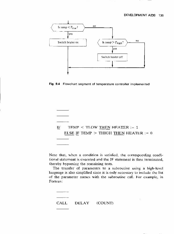
DEVELOPMENT AIDS 135
/ Istemp<rtoM; ? \- no
'
yes'
noSwitch heater on / Is temp > 7^?
^yes
Switch heater off
'1
1
'
'
Fig. 9.4 Flowchart segment of temperature controller implemented
IF TEMP < TLOW THEN HEATER := 1
ELSE IF TEMP > THIGH THEN HEATER :=
Note that, when a condition is satisfied, the corresponding condi-
tional statement is executed and the IF statement is then terminated,
thereby bypassing the remaining tests.
The transfer of parameters to a subroutine using a high-level
language is also simplified since it is only necessary to include the list
of the parameter names with the subroutine call. For example, in
Fortran:
CALL DELAY (COUNT)

136 DEVELOPMENT AIDS
could be used to transfer a value - stored in memory with symbolic
name COUNT -to a subroutine which, say, computes a variable
delay. Similarly results can also be returned from a subroutine in the
same way:
CALL COMPUTE (VALUE 1, VALUE 2, RESULT)
The ability to assign a single symbolic name to a list of values is
illustrated in the following example. The code is in Basic and simply
reads 100 values from an input device and stores them in a table
which has a single name TABLE:
20 FOR 1=1 TO 100
21 INPUT TABLE (I)
22 NEXT I
The FOR statement is used to repeat the input operation 100 times
for 1=1 to 100.
Many microprocessors provide only the two arithmetic operations
for addition and subtraction and consequently it is necessary to write
small programs to compute additional arithmetic functions. High-level languages, therefore, often provide previously written sections
of code which compute frequently required complex arithmetic ex-
pressions. These are known as library functions and it is possible for a
user to simply use the function names in normal arithmetic state-
ments. For example, assuming two library functions to compute the
sine and cosine of an angle are available, the following type of
arithmetic statement may be used:
SUM = SIN (A) + COS (B)
where SUM, A and B are all symbolic variable names. In addition,
users may write their own arithmetic functions and use these in
the program as required. Again, these features are only intended as
examples of those available with a high-level language.

DEVELOPMENT AIDS 137
9.3.4 Editors
When a program has been written either in assembly language or a
high-level language, it is entered into the MDS via a keyboard and,
for example, a visual display. The latter is used simply to show the
user what has been typed and hence what has been input into the
system memory. The source program, therefore, appears simply as a
string of characters corresponding to each program statement.
The compiler program is then run and this reads and translates
each program statement into its equivalent machine language form. If
the resulting machine language program does not perform the re-
quired task, however, there are clearly errors in the source programwhich must be corrected.
All translator programs have diagnostic facilities which help the
user to identify programming errors. In addition, there is a system
program called the editor which enables the user to readily modifythe source program code. This therefore avoids the user having to
revise and type out the entire program again. An editor program is
given commands via the keyboard and is therefore said to run
interactively. Typical editor commands available are:
list a specified number of lines of source code on the
visual display screen
move to a specified line in the source programdelete a specified line(s) of code
insert one or more lines of code
9.3.5 In-circuit Emulators
All the facilities mentioned so far have been programming aids which
are intended to help the user to develop and write application
software. An MDS also optionally provides a hardware development
facility called an in-circuit emulator (ICE).
An ICE is designed to emulate the microprocessor being used in
the system under development, but since it is itself part of the MDSand therefore under the control of the MDS processor, it is possible
to monitor the behaviour of the system under development while it is
operating. This is illustrated in Fig. 9.5.
The system under test is often referred to as the target system andthe ICE behaves exactly as the target processor. It reads the correct
sequence of program instructions from the target memory and gener-
ates the correct bus signals during their execution. It is hence possible
to keep a record, in an area of the MDS memory, of the sequence of
actions of the target processor. This record is known as a real-time

138 DEVELOPMENT AIDS
System under development
r____I___
n
CPUremoved
i i
Memory and I/O
((\\
MDS processor, memory and I/Ol
ICE
II
|
MDS system
Fig. 9.5 In-circuit emulation
trace and it can be examined later by the MDS system software to
locate possible errors. The real-time trace can include some logic
signals obtained from anywhere in the target system. This is a useful
facility for determining hardware faults. The complete sequence
usually required to develop a piece of application software using an
MDS can be summarised as follows:
1 Design a flowchart which performs the required task.
2 Code the program using either assembly language or a high-
level language.
3 Enter this source program into the MDS memory.
4 Assemble or compile the source code to produce the corres-
ponding machine language (object) code.
5 Run the object program.
6 If necessary, debug (i.e. locate errors in) the program using
ICE.
7 Edit the source program and return to 4. until the target system
correctly works.

DEVELOPMENT AIDS 139
Summary
For those applications which require only a small amount (<1Kbytes) of software it is feasible to use a single board system for its
development. For larger applications, however, it is advantageous to
use a development system (MDS).
When using a single board system it is necessary to write all
software in assembly language and perform a partial translation
process by hand.
When using an MDS, in addition to assembly language it is
possible to use a high-level language. This can result in a considera-
ble reduction in program development time.
An MDS also contains an editor program which facilitates the
modification of a source program and possibly an in-circuit emulator
(ICE) to aid the development of the application hardware.

Appendix 1 The Intel 8085Instruction Set
The information in the tables in this appendix are reproduced by
courtesy of Intel Corporation. The following symbols and abbrevia-
tions are used.
A, B, C, D, E, H, L represent one of the internal processor registers
M represents the memory address currently held in
register pair HLbyte represents an 8-bit (2 hex character) data quan-
tity
dble represents a 16-bit (2 byte) data quantity
addr represents a 16-bit (2 byte) memory address
port represents an 8-bit I/O port address
Register pairs are denoted as follows:
PSW represents register pair AFB represents register pair BCD represents register pair DEH represents register pair HLSP represents the 16-bit stack pointer
PC represents the 16-bit program counter
The processor flag bits are
CY carry flag
Z zero flag
S sign flag
P parity flag
AC auxilliary carry
140

APPENDIX 1 THE INTEL 8085 INSTRUCTION SET 141
Data Transfer
GroupThis group of instructions transfers data to and from registers and
memory. No condition flags are affected by any instructions in this
group.
Move
MOV-
MOV-
MOV-
MOV
Move (contd.)
"A, A 7F "E,A 5FA,B 78 E,B 58
A,C 79 E,C 59
A,DA, E
7A7B
MOV- E,DE, E
5A5B
A,H 7C E,H 5CA,L 7D E,L 5D_A,M 7E _E,M 5E
"B,A 47 "H,A 67
B,B 40 H, B 60
B,C 41 H, C 61
B,DB,E
42
43MOV- H,D
H,E62
63
B,H 44 H,H 64
B,L 45 H,L 65
_B,M 46 _H,M 66
"C,A 4F "L,A 6FC,B 48 L,B 68
C,C 49 L,C 69
C,D 4A MOV- L,D 6AC,E 4B L,E 6BC, H 4C L,H 6CC,L 4D L, L 6D_C,M 4E _L,M 6E
~D,A 57 "M,A 77
D,B 50 M,B 70
D, C 51 M,C 71
D,D 52 MOV- M,D 72~ D,E 53 M,E 73
D,H 54 M,H 74
D,L 55 _M,L 75
J),M 56
Move Immediate
"A, byte 3EB, byte 06
C, byte 0ED, byte 16
E, byte IEH, byte 26
L, byte 2E_M, byte 36
MVI-
Load Immediate(Reg. Pair)
"B, dble 01
LXI- D, dble 1
1
_H, dble 21
SP, dble 31
Load/Store A direct
LDA addr 3ASTA addr 32
Load/Store A indirect
LDAX B 0ALDAX D 1ASTAX B 02
STAX D 12
Load/Store HL direct
LHLD addr 2ASHLD addr 22
Exchange HL/DEXCHG EB

142 APPENDIX 1 THE INTEL 8085 INSTRUCTION SET
Data This group of instructions performs arithmetic operations on data in
Manipulation registers and memory.
Group - Arithmetic
Add/Subtract Immediate* Double AddfAdd"
ADD-
ABCDEHLM
ADC-
SUB-
Subtract*
'A
BCDEHLMABCDEHLM
SBB-
87
80
81
82
83
84
85
86
B 88
C 89
D 8AE 88
H 8CL 8DM 8E
97
90
91
92
93
94
95
96
9F98
99
9A9B9C9D9E
ADI byte
ACI byte
SUI byte
SBI byte
C6CED6DE
DAD-
Increment/Decrement 51
INR-
ABCDEHLM
3C04
0C14
1C24
2C34
DCR-
Increment/Decrement Register Pairft
INX-
BDHSP
03
13
23
33
"B 09
D 19
H 29_SP 39
A 3DB 05
C 0DD 15
E IDH 25
L 2DM 35
-t
B 0BD IBH 2BSP 3B
DCX-
Complement/Set CYf
CMC 3FSTC 37
Decimal Adjust A*
DAA 27
Complement Att
CMA 2F
Note
* All flags (CY, Z, S, P, AC) affected** All flags except carry affected
t Only carry affected
tt No flags affected

APPENDIX 1 THE INTEL 8085 INSTRUCTION SET 143
DataManipulation
Group -Logical
This group of instructions perform logical operations on data in
registers and memory.
Note
AND* OR* Exclusive-OR*
[A A7 "A B7 "A AFB A0 B BO B A8C Al C Bl C A9
ANA- DE
A2A3
ORA- DE B3
XRA" D AAE AB
H A4 H B4 H ACL A5 L B5 L AD_M A6 _M B6 _M AE
ANI byte E6 ORI byte F6 XRI byte EE
Compare*
BFB8B9
Rotate f
RLC 07"ABC
CY <
—
- 7<
CMP- DEHL
BABBBCBD
RRC OF 7 >0 -—
>
CY
_M BE
CPI Dyte FERAL
RAR
17
IF
CY «
—
- 7< J
7 >0 —
i
> CY —
All flags affected
t Only carry affected
Transfer of
Control GroupThis group of instructions alter normal sequential program flow. The
following condition codes are used:
NZ not zero (Z = 0)
Z zero (Z=l)
NC no carry (CY = 0)
C carry (CY=1)
PO parity odd (P = 0)
PE parity even (P = 1)
P plus (S = 0)
M minus (S = 1)

144 APPENDIX 1 THE INTEL 8085 INSTRUCTION SET
Jump Call Return
Input/Output
Group
JMP addr C3JNZ addr C2JZ addr CA
JNC addr D2JC addr DA
JPO addr E2JPE addr EAJP addr F2JM addr FA
Jump Indirect
PHCL E9
CALL addr CDCNZ addr C4CZ addr CC
CNC addr D4CC addr DC
CPO addr E4CPE addr ECCP addr F4CM addr FC
RET C9RNZ CORZ C8
RNC DORC D8
RPO EORPE E8RP FORM F8
This group of instructions perform I/O operations between the A-
register and a specified port.
IN port DBOUT port D3
Machine Control
GroupThis group of instructions manipulate the contents of the stack and
alters/controls the state of the processor.
Stack Operations (Register Pairs)
PUSH-
XTHL
SPHL
BDHLPSW
E3
F9
C5 "B CID5E5
POP- DH
DlEl
F5 _PSW Fl
(L)«->((SP))
(H)**((SP) + 1)
(SP)«-(H) (L)
Interrupt Control
EI FB (Enable Interrupts)
DI F3 (Disable Interrupts)
RIM 20 (Read Interrupt Mask)SIM 30 (Set Interrupt Mask)
Processor Control Operations
Restart Control
NOP 00
HLT 76
(No Operation)
(Halt)
RST-
C7CFD7DFE7EFF7FF

Appendix 2 BinaryMultiplication and Division
Since many 8-bit microprocessor applications require only the basic
arithmetic operations of addition and subtraction, most 8-bit micro-
processors do not have multiplication or division instructions. If mul-
tiplication or division is required it is necessary therefore to write
subroutines to perform these functions. This appendix presents,
firstly, an algorithm for the binary multiplication of two 8-bit num-bers to produce a 16-bit product and an algorithm for the binary
division of a 16-bit number by an 8-bit number to produce an 8-bit
quotient. Unsigned binary number representation is assumed for each
algorithm. Secondly, signed binary multiplication is presented.
A2.1 Unsigned The following example given in Fig. A2.1 shows that the multipli-
MuImplication cation of two 8-bit binary numbers produces a 16-bit product. Eachbit of the multiplier is tested in turn, starting with the least significant
bit. The operation to be performed as each bit is tested is to simply
add the multiplicand - suitably shifted -to the partial (running) pro-
duct if the multiplier bit is a 1 or to add zero if the multiplier bit is a
0. This is shown in Fig. A2.1.
To implement this process in an 8-bit microprocessor efficiently, it
is advantageous to modify the sequence in which the partial products
are produced in order to make maximum use of the instructions
available. For example, since the final product requires 16 bits, it is
convenient to use a combined register pair to hold the accumulatedproduct. Thus, if this is register pair HL and the multiplicand is held
in another register pair, the double add instruction can be used to
sum each partial product. To obtain the appropriate weighting of
each partial product, it is necessary to shift the combined contents of
HL as each multiplier bit is tested. This can best be accomplished by
145

146 APPENDIX 2 BINARY MULTIPLICATION AND DIVISION
Multiplicand
Multiplier
Partial product
Partial product
Partial product
Partial product
Partial product
Partial product
Partial product
Partial product
Final product
1101101100110101
000000000000000011011011
000000001101101100000000
000000001101101111011011
000001000100011100000000
000001000100011111011011
000100011111011111011011
001011010101011100000000
0010110101010111000000000010110101010111
i.e. 219i.e. 53
Multiplier bit = 1
Multiplier bit =
Multiplier bit = 1
Multiplier bit =
Multiplier bit = 1
Multiplier bit = 1
Multiplier bit =
Multiplier bit =
i.e. 11607
Fig. A2.1 Binary multiplication
Assembly Instructions Comments
MVI B, 08 (B) - 8
LXI H, 0000 (H) (L)-
LABI: DAD H (H)(L)*-(H)(L) + (H)(L)
RLC Rotate multiplier bit to CY.
JNC LAB2 CY=1?
DAD D Yes: (H) (L)-(H) (L) + (D) (E)
LAB2: DCR B (B)~- (B)-l
JNZ LABI Count zero?
HLT Yes: halt.
Fig. A2.2 Unsigned multiplication program

APPENDIX 2 BINARY MULTIPLICATION AND DIVISION 147
BEGIN
Initialise partial product count,
Initialise HL to zero.
Shift (H) (L) left 1 place.
Shift (A) left 1 place.
Is carry flag = 1 ?
yes
Add multiplicand to
running product.
Decrement count.
Is count = 0?
yes
Fig. A2.3 Unsigned multiplication flowchart
testing the multiplier bits starting with the most significant and
shifting the contents of HL left by again using the double addinstruction to add the contents to itself (x 2). If the multiplier is held
in the A-register, each bit may be tested by shifting the contents left
one place and testing the carry flag. The complete algorithm is as
follows.
Let A hold the multiplier
B hold a count of the number of partial products
DE hold the multiplicand - m.s. byte is zero
HL hold accumulated product
A flowchart can now be developed, as shown in Fig. A2.3. Thecorresponding program is given in Fig. A2.2.

148 APPENDIX 2 BINARY MULTIPLICATION AND DIVISION
A2.2 Division The division process is analogous to the multiplication process just
considered except that, with division, repeated subtractions are per-
formed in place of additions. The process is illustrated by means of
an example. The example considered is shown in Fig. A2.4 and
illustrates the division of a 16-bit number (the dividend) by an 8-bit
number (the divisor) to produce an 8-bit result (the quotient). The
first subtraction operation does in fact produce a ninth quotient bit
but this is normally zero unless the most significant byte of the
dividend is greater than the divisor. To allow for this eventuality,
however, the additional (ninth) quotient bit is stored in the carry bit
in the program which follows.
Divisor (i.e. 148) = 10010100
Q =CY = 1
Restore P.R.
CY = 1 :. QRestore P.R.
CY = 1 /. QRestore P.R.
CY =
CY = 1
Restore P.R
CY = :.
CY = 1 :.
Restore P.R
CY = 1 .. QRestore P.R.
CY
= 1
=
=
=
:. Q = 1
000101001 = Quotient i.e. 41
) 000101 11 101 10100 = Dividend i.e. 6068- 100 lOlOO l
1000001 If
00101111- 1001010010011011"01011110
- 10010100nooioiof10111101
- 10010100?001010011-10010100lOllllllf10100110
-10010100?000100101-1001010010010001?01001010
- 1001010010110110?10010100
- 1001010000000000 = Remainder (i.e. zero)
Fig. A2.4 Binary division
Fig. A2.4 shows that the individual quotient bits are determined by
subtracting the appropriately shifted divisor from the partial remain-
der (P.R.). If the result of the subtraction is positive (CY = 0), the
divisor is less than the partial remainder, hence the division is correct
and the quotient bit is a 1. If the result of the subtraction is negative
(CY= 1), the division is incorrect and hence the quotient bit is a
and the previous partial remainder is restored. This operation is
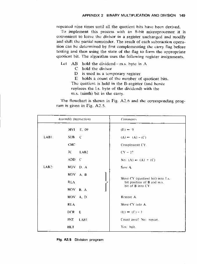
APPENDIX 2 BINARY MULTIPLICATION AND DIVISION 149
repeated nine times until all the quotient bits have been derived.
To implement this process with an 8-bit microprocessor it is
convenient to leave the divisor in a register unchanged and modifyand shift the partial remainder. The result of each subtraction opera-
tion can be determined by first complementing the carry flag before
testing and then using the state of the flag to form the appropriate
quotient bit. The algorithm uses the following register assignments.
Let AB hold the dividend - m.s. byte in AC hold the divisor
D is used as a temporary register
E holds a count of the number of quotient bits.
The quotient is held in the B -register (and hence
replaces the l.s. byte of the dividend) with the
m.s. (ninth) bit in the carry.
The flowchart is shown in Fig. A2.6 and the corresponding prog-
ram is given in Fig. A2.5.
Assembly Instructions Comments
MVI E, 09 (E)— 9
LABI: SUB C (A)*- (A) -(C)
CMC Complement CY.
JC LAB2 CY = 1?
ADD C No: (A) - (A) + (C)
LAB 2: MOV D, A Save A.
MOV A, B 1
RLA >
MOV B, A J
Move CY (quotient bit) into
bit position of B and m.s.
bit of B into CY.
.s.
MOV A, D Restore A.
RLA Move CY into A.
DCR E (E) - (E) - 1
JNZ LABI Count zero? No: repeat.
HLT Yes: halt.
Fig. A2.5 Division program

150 APPENDIX 2 BINARY MULTIPLICATION AND DIVISION
(begin)
Initialise quotient count.
Subtract divisor from
partial remainder.
Is carry flag = 0?
yes
Restore partial remainder.
Rotate combined carry
and 16-bit partial remainder
1 place left.
Is count = 0?
yes
(END
Fig. A2.6 Division flowchart
A2.3 Signed
Binary
Multiplication
This section describes a program for the multiplication of two 8 -bit
two's complement signed binary numbers to produce a 16-bit two's
complement signed product.
A2.3.1 The Algorithm
The basic multiplication process for two 8-bit positive numbers is
illustrated by the example of Fig. A2.7.
Since each multiplier bit can only be or 1, the multiplication
process is simply to add the multiplicand (suitably shifted) to the
partial product if the multiplier bit is a 1 or to add zero if the
multiplier bit is a 0. This process is repeated eight times until all the

APPENDIX 2 BINARY MULTIPLICATION AND DIVISION 151
Multiplicand 01001001 = +73Multiplier 00001111 = + 15
Partial product 00000000 00000000Add multiplicand 01001001 Multiplier bit =
1
Partial product 00000000 01001001Add multiplicand 1001001 Multiplier bit =
1
Partial product 00000000 11011011Add multiplicand
Partial product
01 001001 Multiplier bit =1
- 00000001 11111111
Add multiplicand
Partial product
010 01001 Multiplier bit =1
= 00000100 01000111Add zero
Partial product
0000 0000 Multiplier bit =
= 00000100 01000111Add zero
Partial product
00000 000 Multiplier bit =
00000100 01000111Add zero 000000 00 Multiplier bit =
Partial product = 00000100 01000111Add zero 0000000 Multiplier bit =
Final product = 00000100 01000111 = +1095
Fig. A2.7 Signed multiplication (Example 1)
multiplier bits have been considered. The correct signed 16-bit
product is produced.
Unfortunately, the above process does not hold for the multiplica-
tion of mixed two's complement signed numbers and certain correc-
tions have to be made to produce the correct signed product. Aconvenient method for automatically obtaining these corrections is
1 Extend the multiplicand by copies of its most significant bit - 0s
if the multiplicand is positive, Is if it is negative.
2 Subtract the final partial product.
This is illustrated, in Fig. A2.8, by an example involving a negative
multiplier and multiplicand.
A2.3.2 The Subroutine
Since the multiplicand and the accumulated product both require 16
bits, it is convenient to use two pairs of registers to hold them during
the multiplication process. The processor register assignments are
DE holds the multiplicand
HL holds the accumulated product
A holds the multiplier
B holds the bit count

152 APPENDIX 2 BINARY MULTIPLICATION AND DIVISION
Multiplicand 11111111 10110111 = -73 (extended by copies
Multiplier 11110001 = -15 of itsm.s. bit)
Partial product = 00000000 00000000
Add multiplicand 11111111 10110111 Multiplier bit = 1
Partial product 11111111 10110111
Add zero 00000000 0000000 Multiplier bit =
Partial product = 11111111 10110111
Add zero 00000000 0000000 Multiplier bit =
Partial product = 11111111 10110111
Add zero
Partial product
00000000 00000 Multiplier bit =
11111111 10110111
Add multiplicand 11111011 0111 Multiplier bit = 1
Partial product 11111011 00100111
Add multiplicand 11110110 111 Multiplier bit = 1
Partial product = 11110010 00000111
Add multiplicand 11101101 11 Multiplier bit = 1
Partial product = 11011111 11000111
Subtract multiplicand
Final product =
11011011 1 Multiplier bit = 1
= +109500000100 01000111
Fig. A2.8 Signed multiplication (Example 2)
The multiplication process used in the program is slightly different
from that described above in that the partial products are produced
in the reverse order and start with the most significant. This has been
done because, in the Intel 8085, the contents of a register pair can
only be shifted left. This is accomplished by using the double add
instruction to add the contents of the register pair to itself.
The HL register pair is also used as a parameter passing mechan-
ism when the subroutine is entered. The contents of HL point to the
area of memory where the multiplicand and the multiplier are stored
and, on leaving the subroutine, the product is stored immediately
following these values as illustrated in Fig. A2.9.
A flowchart for the algorithm is given in Fig. A2.10 and the
corresponding assembly language subroutine shown in Fig. A2.ll.
(H)(L) on entering -
(H) (L) on leaving
multiplicand
multiplier
m.s. byte of product
l.s. byte of product
Fig. A2.9 Memory pointer use

APPENDIX 2 BINARY MULTIPLICATION AND DIVISION 153
Initialise
register <
contents
Subtract final
partial product
Extend multiplicand
by copies of its m.s.
bit
Set bit count }
Test remaining <
7 bits
(begin)
Load multiplicand into E.
Load multiplier into A.
Clear (D).
Clear (H) (L)
is m.s. on ui nuiu piici i :
Jyes
(H)(L)«-(H)(L)-- (D) (E)
_
' '
/ Is m.s. bit of multiplicand = 1?
yes
Load FF(hex) into D.
Set bit count = 7.
Shift (H) (L) left 1 place.
Shift (A) left 1 place.
Count = 0?
yes
(end^)
/ m c hit of A - 1 ? \ no
'
yes
(H)(L)*-(H)(L) + (D)(E)
'
Decrement bit count.
'
Fig. A2.10 Signed multiplication flowchart

154 APPENDIX 2 BINARY MULTIPLICATION AND DIVISION
Assembly Instructions
MULT: PUSH PSW
PUSH B
PUSH D
MOV E, M
MOV B, E
INX H
MOV A, M
MOV C, A
PUSH H
LXI H, 0000
MVI D, 00
RPOS:
DPOS:
ANA A
JP RPOS
MOV A, E
CMA
INR A
MOV E, A
DAD D
MOV A, B
ANA A
JP DPOS
MVI D, FF
MOV E, C
MOV A, B
MVI B, 07
}
Comments
}
Save register contents.
Load multiplicand into E and save in B.
Load multiplier into A and save in C.
Save and clear (H) (L).
Clear (D).
m.s. bit of multiplier - 1?
Yes - subtract final partial product.
m.s. bit of multiplicand - 1?
Yes - load FF (hex) into D (extend sign).
Restore multiplicand into E and multiplier
into A.
Set bit count = 7

APPENDIX 2 BINARY MULTIPLICATION AND DIVISION 155
NEXT: DAD H Shift (H) (L) left 1 place.
RLC Shift (A) left 1 place.
ANA A
JP ZERO m.s. bit A= 1?
DAD D Yes — add multiplicand.
ZERO: DCR B Decrement count.
JNZ NEXT Branch back if count not zero.
XCHG Save product in DE.
POP H Restore memory pointer.
INX H Increment.
MOV M, D 1
INX > Store product in memory.
MOV M, EJ
POP D "I
POP B S Restore register contents.
POP PSW J
RET Return.
Fig. A2.11 Signed multiplication subroutine

Appendix 3 MicroprocessorCharacteristics
In order to avoid describing the many small differences between one
type of microprocessor and another, the main body of the text has
concentrated on a single popular microprocessor system - the Intel
8085. It is thus possible to illustrate simply the fundamental charac-
teristics which are applicable to any microprocessor: the techniques
for programming one device apply, in general, to any other type. This
appendix has been included, however, to give a brief summary of the
main features of some of the other popular microprocessors which
are currently available and, where appropriate, to indicate how they
differ from the Intel 8085.
It is convenient to break other microprocessors into three
categories:
1 Other 8-bit microprocessors - this includes devices like the
Rockwell R6500, Zilog Z80 and Motorola MC6800/9 which
require multiple chips - microprocessor, memory, Pl/O-to
create a microcomputer system.
2 Single-chip microcomputers - this includes devices like the
Texas Instruments TMS1000, Intel 8048 and Motorola
MC6801 which incorporates the microprocessor, a limited
amount of memory (ROM and RAM), I/O facilities, and a
counter timer on a single integrated circuit chip.
3 \6-bit microprocessors - this includes devices like the Texas
Instruments TMS9900, Intel 8086, Zilog Z8000 and Motorola
MC68000 which are large, high-performance chips intended
primarily for those minicomputer-type application areas which
require either substantial amounts of random access memory(>64K bytes) or more sophisticated computational facilities (16
or more bits, hardware multiply and divide, etc.).
Some of the characteristics of the devices in these categories are
discussed in the following sections.
156

APPENDIX 3 MICROPROCESSOR CHARACTERISTICS 157
A3.1 Other 8-bit
Microprocessors
A3.1.1 Zilog Z80
Although the instruction mnemonics used by Zilog are different from
the 8085, the instruction set of the Z80 microprocessor embodies all
the instructions of the 8085 (except RIM and SIM) plus someadditional instructions. These include bit manipulation instructions
which allow individual bits within a byte to be set, reset or tested with
a single instruction, and also some block transfer instructions which
allow multiple bytes of data to be moved from one area of memory to
another. In addition, the Z80 contains over twice the number of
internal processor registers as the 8085, mainly organised as an
alternative register set. These are shown in Fig. A3.1.
Although the complete instruction set operates with the main block
of registers, it is possible to exchange the contents of the two sets
with just two instructions. Hence an interrupt service routine, for
example, can use one set of registers for data manipulation whilst the
main program uses the other set.
Main Register Set Alternate Register Set
A F
B C
D E
H L
A' F'
B' C
D' E'
H' V
Stack Pointer SP
Program Counter PC
Index Register IX
Index Register IY
> 1 6-bit registers
Fig. A3.1 Z80 processor registers
The two index registers can be used to provide additional register
indirect addressing features. For example, the instruction
LD(IX+6),C
results in the contents of register C being stored in the memorylocation whose address is the current contents of the 16-bit index
register IX plus 6.

158 APPENDIX 3 MICROPROCESSOR CHARACTERISTICS
The Z80 also has available additional relative jump instructions.
These are particularly useful since they allow the programmer to define
a destination branch address relative (±128) to the jump instruction
itself and hence a program segment employing only relative jumps
can be relocated without affecting its operation.
A3.1.2 Motorola MC6800/9
The MC6809 is a development of the earlier MC6800. Like the Z80it has two 16-bit index registers and two separate 16-bit stack pointer
registers. The latter are used in the conventional manner but are
useful when the system contains two types of program - a system
program and a user program. Each program may then use a sepa-
rately defined area of memory as a stack.
Like the earlier 6800, the 6809 employs only two 8-bit working
registers but the instruction set includes some 16-bit instructions and
also an unsigned 8x8 bit multiply instruction which produces a
16-bit product. It also has available extensive relative addressing
instructions to allow the programmer to write position-independent
code.
A summary of the MC6809 register set is shown in Fig. A3. 2.
A B
Program Counter PC
System Sack Pointer SP
User Stack Pointer SP'
Index Register IX
Index Register IY
Data Manipulation
Registers
Address Registers
Fig. A3.2 MC6809 processor registers
A3.2 Single-chip
MicrocomputersA3.2.1 Intel 8048 Family
The 8048 family encompasses a number of devices with from IK to
4K bytes of program ROM or EPROM and 64 to 256 bytes of RAMon the chip. In addition, the chip provides three 8-bit I/O ports and a
separate timer/event counter.

APPENDIX 3 MICROPROCESSOR CHARACTERISTICS 159
32<
16<^
General
RAMArea
Bank
Stack —
8 levels
BankO
Single working register
RAM areas are software
selected to be active
one at a time; first
two registers in each bankare memory pointers.
IK - 4 KROM/EPROM
PortO
Port l
Port 2
•Interrupt
Timer/Event Counter
Fig. A3.3 The Intel 8048
The 8048 implements many of the instruction types provided by
the 8085 and includes individual bit set and reset instructions. The
stack area is obviously limited but can support up to 8 levels of
subroutine calls. Similarly, there is just a single interrupt input line. Aschematic diagram of the 8048 is shown in Fig. A3. 3. Other members
of the 8048 family include versions with EPROM in place of ROMfor program development and also a device - the 8022 - which has an
additional ADC on the chip.
A3.2.2 Motorola MC6801/5
The 6801 is a single chip version of the earlier 6800 with some
additional instructions. It contains 2K bytes of on-chip ROM, 128
bytes of RAM, four parallel I/O ports, three serial I/O lines, and
three 16-bit timer/event counters. The processor architecture itself is
similar to the 6800, consisting of a 16-bit program counter, stack
pointer and index register, and also an 8-bit working register. The
instruction set is in general similar in character to the 8085 but in
addition contains an 8x8 bit multiply instruction.
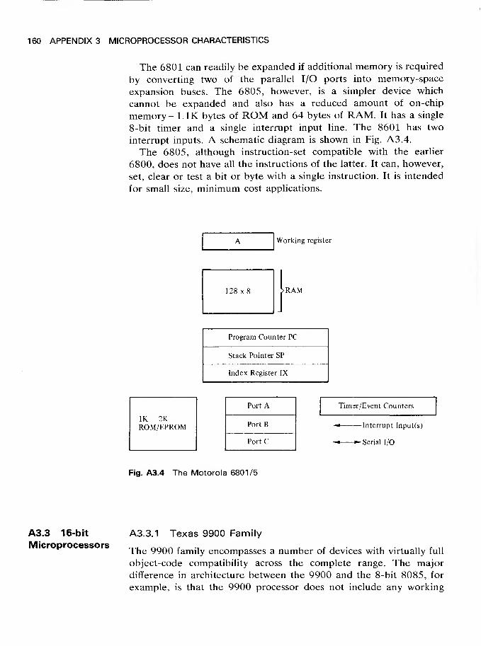
160 APPENDIX 3 MICROPROCESSOR CHARACTERISTICS
The 6801 can readily be expanded if additional memory is required
by converting two of the parallel I/O ports into memory-space
expansion buses. The 6805, however, is a simpler device which
cannot be expanded and also has a reduced amount of on-chip
memory- 1.1K bytes of ROM and 64 bytes of ELAM. It has a single
8-bit timer and a single interrupt input line. The 8601 has two
interrupt inputs. A schematic diagram is shown in Fig. A3.4.
The 6805, although instruction-set compatible with the earlier
6800, does not have all the instructions of the latter. It can, however,
set, clear or test a bit or byte with a single instruction. It is intended
for small size, minimum cost applications.
Working register
128x8 >RAM
Program Counter PC
Stack Pointer SP
Index Register IX
1K-2KROM/EPROM
Port A
PortB
PortC
Timer/Event Counters
-Interrupt Input(s)
-Serial I/O
Fig. A3.4 The Motorola 6801/5
A3.3 16-bit
MicroprocessorsA3.3.1 Texas 9900 Family
The 9900 family encompasses a number of devices with virtually full
object-code compatibility across the complete range. The major
difference in architecture between the 9900 and the 8-bit 8085, for
example, is that the 9900 processor does not include any working

APPENDIX 3 MICROPROCESSOR CHARACTERISTICS 161
registers (A, B, C, D, etc.) but instead contains a pointer -theworkspace pointer - to a 32-byte area of RAM which is then used to
provide sixteen 16-bit processor registers. This has the disadvantage
that different segments of a program must first choose the workspace
in memory that contains the appropriate set of working registers used
by the instructions in that segment. The major attraction, however, is
that it allows rapid switching between a large number of alternative
register groups. This is particularly helpful if a large number of
different interrupts are to be serviced - the 9900 provides for sixteen
levels of priority vectored interrupt. Each interrupt service routine
simply switches to its own workspace area thus leaving other work-
space areas intact.
The 9900 like other 16-bit microprocessors contains a muchricher -more sophisticated - instruction set than the 8-bit micro-
processors. For example, the data manipulation group includes multi-
ply and divide instructions, logical and multiple bit shifts, and also
instructions to operate on words, bytes or bits.
The 9900 itself is just the processor chip and thus requires external
ROM, RAM and I/O circuitry. The 9940, however, is the single-chip
version and contains 2K bytes of EPROM/ROM and 128 bytes of
RAM on the same chip. The RAM is divided into four 32-byte
workspace areas to support the four levels of priority vectored
interrupt that can be serviced. The 9940 also provides up to 32
parallel I/O lines and two additional serial-in, serial-out lines. Aschematic diagram of this device is shown in Fig. A3. 5.
Program Counter PC
Workspace Pointer WP
32 x8
32 x8
32 x8
32 x8
>RAM
Four workspace areas
each containing 1
6
general purpose
1 6-bit registers
2Kx8ROM/EPROM
•32 I/O lines
Serial I/O
Fig. A3.5 The Texas 9940

162 APPENDIX 3 MICROPROCESSOR CHARACTERISTICS
A3.3.2 Intel 8086
The 8086 has a directly addressable memory space of 1 megabyte
and a rich instruction set. It employs a 6-byte look-ahead (pre-fetch)
instruction queue which ensures fast instruction execution times and
it is therefore ideal for applications which require either a high
system throughput or large memory space (ROM and RAM). Theprocessor is divided into two sections: the execution unit (EU) which
contains four 16-bit data (working) registers, two index registers, and
two pointer registers; and a bus interface unit (BIU) which contains
the 6-byte pre-fetch instruction queue and the relocation register file
containing the program counter and four segment registers. Thelatter can be used by the programmer to set up four areas of
memory: a program area, a stack area, and two data areas. Each area
or segment can be up to 64K bytes.
While the 8086 is internally decoding and executing the current
instruction, the BIU fetches the next sequential instruction - up to 6
bytes - from memory and stores this in the pre-fetch queue. Thus,
assuming that the current instruction is not a jump instruction, it is
immediately available to the EU upon completion of the current
instruction. If the current instruction is a jump instruction, however,
the next instruction is fetched from memory in the conventional way.
The instruction set includes 8 and 16-bit signed and unsigned
arithmetic in binary or decimal, including multiply and divide. In
addition, it contains extensive bit, byte, word and block instructions.
A schematic diagram of the processor is shown in Fig. A3. 6.
A3.3.3 The Zilog Z8000
The Z8000 is one of the most powerful 16-bit microprocessors (as in
the MC68000) with a very advanced architecture comparable with
many minicomputers. The processor can address up to 8M words of
memory in 64K word segments. A schematic diagram of the proces-
sor registers is shown in Fig. A3. 7.
The processor maintains two separate types of stack: one for use in
special mode by the system's programmer - this is useful, for exam-ple, when implementing the system software for sophisticated multi-
programming applications - and the other for use as normal user
stack pointers.
The sixteen 16-bit general purpose registers can be used either as
data registers or as address registers - for example, as index registers.
The data manipulation instructions include signed multiply anddivide and can operate on single bits, BCD nibbles (half-bytes), 8-bit

APPENDIX 3 MICROPROCESSOR CHARACTERISTICS 163
Program Counter PC
4 Segment Address
pointers
Instruction
Pre-fetch
queue
BIU
Fig. A3.6 The Intel 8086
Stack Pointer SP
Data Pointer BP
Index Register SI
Index Register DI
AH I AL
BH jBL
CH |CL
DH ! DL
EU
Segment Address
Program Counter
Normal Stack pointer
Normal Stack pointer
System Stack pointer
System Stack pointer
16
General purpose register
General purpose register 1
General purpose register 1
5
Fig. A3.7 Z8000 register set
bytes, 16-bit words, or 32-bit double words. Similarly, the data
movement instructions are very extensive and include a comprehen-
sive set of block and string (group of characters) transfer instructions.

Solutions to Exercises
CHAPTER 1
1.1 35 = 00100011
67 = 01000011
224=11100000
1.2 00010111 = 23
01010101 = 85
11011011 = 219
1.3 27= 00011011= IB (hex)
96= 01100000= 60 (hex)
3334= 110100000110 = D06 (hex)
1.4 D3= 11010011= 211
2F= 00101111= 47
2D9E=0010110110011110=11678
CHAPTER 2
2.1 10 bits have 1024 (IK) binary combinations.
4 bits have 16 binary combinations (0000—» 1111).
14 bits can address 16K bytes of memory.
Memory Address
(hex)
FFFF
1100
10FF
10000FFF
8 bits
0000
2.2 1024 (IK) locations require 10 bits.
4096 (4K) locations require 12 bits.
256 locations require 8 bits.
164

SOLUTIONS TO EXERCISES 165
2.3 Since the m.s. bits of the address space are not used for memory (ROM or
RAM), suitable I/O port addresses are:
1100210041008100
2.4 0000 -> 0FFF = ROM - 12 bits - 4K bytes
2000-^21FF = RAM= 9 bits = 5 12 bytes
4000 -> 400F = I/O = 4 bits = 16 ports
CHAPTER 3
3.1Assembly Instructions
MVI B, 87
MOV A, B
MOV C, B
MVI D, 2F
MOV E, D
LXI H, 8EF2
Comments
(B) — 87 (hex)
(A) - (B)
(C) - (B)
(D) — 2F (hex)
(E) *- (D)
(H)(L)^8EF2(hex)
3.2Assembly Instructions Comments
MVI A, FF (A) — FF (hex)
STA 20FF (20FF) — (A)
LXI H, 20FF (H) (L) — 20FF (hex)
MOV B, M (B) — (20FF)
MOV C, B (C) - (B)
MOV D, B (D) *- (B)

166 SOLUTIONS TO EXERCISES
3.3MEMORY ASSEMBLY
ADDRESS CONT MNEMONIC OP1 OP2
2000 06
MVI B 872001 87
2002 78
MOV A B
2003 48
MOV C B
2004 16
MVI D 2F2005 2F
2006 5A
MOV E D
2007 21
LXI H 8EF22008 F2
2009 8E
3.4 (2080) = 2A (A) = 2A(2020) = 20 (B) = 20
(2021) = 2A (C) = 2A
2 1 20 20, 1 1 80 20, EB, 3E 2A,
77, 3E 20, 47, EB, 70, EB, 4E, 79,
32 21 20, 76.
CHAPTER 4
4.1 Binary Unsigned Binary 2's complement BCI
+ 105 69
+ 40 28
+ 118 76
-120 88
-109 93
-121 87
0110 1001 105
0010 1000 40
01110110 118
1000 1000 136
10010011 147
1000 0111 135

SOLUTIONS TO EXERCISES 167
4.2 103= 01100111+ 27 = +0001 1011
130 1000 0010
67= 01000011118 = +01110U0
185= 10111001
105= 0110 1001
94 = -0101 1110
11 0000 1011
56= 0011100019= -0001 0011
37 0010 0101
4.3 +105= 0110 1001 1
-105= 10010111
94= 0101 1110 J
-105= 10010111
+ 94= +0101 1110
- 11= 1111 0101
+ 56= 0011 1000
- 56= 1100 1000
19 00010011 J
56= 1100 1000
19 = +()001 0011
37' 1101 1011
103= 0110 0111- 27 = -0001 1011
+ 76^ 0100 1100
67= 0100 0011
118= -0111 0110
- 51 1100 1101
4.4 34= 00110100+ 52 = +0101 0010
Normal Binary Sum.•. Correction
1000 0110
+0000 0000
Corrected BCD Sum = 1000 0110
CY = 0, AC =
86
19= 00011001+27 = +0010 0111
Normal Binary Sum = 0100 0000 CY=0, AC=1.-. Correction = +0000 0110
Corrected BCD Sum = 0100 0110 =46

168 SOLUTIONS TO EXERCISES
75= 01110101-42 = -0100 0010
Normal Binary Diff. = 00110011 CY = 0, AC =.-. Correction = +0000 0000
Corrected BCD Diff. = 00110011 =33
81= 1000 0001
-39 = -0011 1001
Normal Binary Diff. = 0100 1000
.-.Correction =+11111010CY = 0, AC=1
Corrected BCD Diff. 0100 0010 42
4.5 Assembly Instructions A etion
MVI A, 13 (A) — 0001 0011
AD1 41 (A) — 0101 0100
DAA (A) - 0101 0100
4.6 Assembly Instructions Action
MVI A, C8
ADI E5
(A) — 1 100 1000 = -56,
(A) — 1010 1 101 = -83
,
4.7
A,B AANDB A ORB AXORB
A= 1010 1110
B = 0001 0100
0000 0100 1011 1110 10111010
A = 0010 1011
B= 1000 1111000 1011 1010 1111 1010 0100
A = 00110111B = 0100 1000
0000 0000 0111 1111 0111 1111
A= 1010 0101
B = 0101 10100000 0000 11111111 1111 1111

SOLUTIONS TO EXERCISES 169
4.8
Assembly Instructions Action
MVI A, 9E (A) - 1001 1110 CY, P not affected
MVI B, A4 (B) - 1010 0100 CY, P not affected
RLC (A) - 0011 1101 CY — 1 , P not affected
ANI C2 (A) - 0000 0000 CY — 0, P— 1
ORA B (A) - 1010 0100 CY— 0,P—
CHAPTER 5
5.1 The program will loop on the instructions
LABI: DCRJNZ
ALABI
until the contents of A become zero. The program will then halt.
5.2 The program will loop on the instructions
LAB2:
5.3
INRJNZ
ALAB2
until the contents of A increments up to FF and then overflows to 00. The zero
flag becomes set and the program will therefore loop 256 times.
Let B hold SUM.C hold INCVAL.
(begin)
Initialise SUM and
INCVAL to zero
Add INCVAL to SUM.
Add 2 to INCVAL.
Is INCVAL = 22?
yes
(end ^
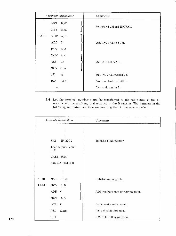
Assembly Instructions Comments
MVI B, 00 1
> Initialise SUM and INCVAL.MVI C, 00 J
LABI: MOV A, B
ADD C K Add INCVAL to SUM.
MOV B, A
MOV A, C ]
ADI 02J>
Add 2 to INCVAL.
MOV C, AJ
CPI 16 Has INCVAL reached 22?
JNZ LABI No: loop back to LABI.
Yes: end; sum in B.
5.4 Let the terminal number count be transferred to the subroutine in the C-register and the resulting total returned in the B-register. The numbers in the
following subroutine are then summed together in the reverse order:
170
Assembly Instructions Comments
LXI SP, 20C2 Initialise stack pointer.
Load terminal count
inC
CALL SUM
Sum returned in B
SUM: MVI B, 00 Initialise running total.
LAB 1 : MOV A, B 1
ADD C ? Add number count to running total.
MOV B, A J
DCR C Decrement number count.
JNZ LABI Loop if count not zero.
RET Return to calling program.

SOLUTIONS TO EXERCISES 171
5.5 Let A hold COUNTB hold LIMIT (passed to subroutine as a parameter)
(BEGIN
Clear COUNT to zero
Increment COUNT by
Is COUNT = LIMIT?
yes
RETURN
Assembly Instructions Comments
LXI SP, 20C2 Initialise stack pointer.
Load LIMIT in B
CALL DLAY
DLAY: PUSH PSW Save (A) and (F) on stack.
MVI A, 00 Clear COUNT.
LABI: INR A 1> Increment COUNT and compare with LIMIT.
CMP B J
JNZ LABI Loop if not equal.
POP PSW Restore (A) and (F) from stack.
RET

172 SOLUTIONS TO EXERCISES
5.6
Assembly Instructions Comments
Main I
Program j
"TIMDLY1:PUSH PSW
LXI H, 2081 1
Store LIMIT value in memory location 2081.Subroutine 1< MVI M, Limit J
CALL DLAY
RET
"DLAY: PUSH PSW
MVI A, 00
LABI: INR A
Subroutine 2< CMP M I
JNZ LABI
POP PSW
RET
As above except COUNT compared with
contents of location 2081.
5.7 The maximum run time of TIMDLY2 is approximately 256 times (00^FF) the
7 instructions in the loop. Therefore
TDLY2 = 256 x 14 = 3584 fxs
Similarly, the maximum run time of TIMDLY1 is approximately 256 times
(00^FF) the maximum run time of TDLY2. Therefore
Tdlyi- 256x3584 /ms
-917.5 ms
Thus the maximum time delay is approximately 920 ms.
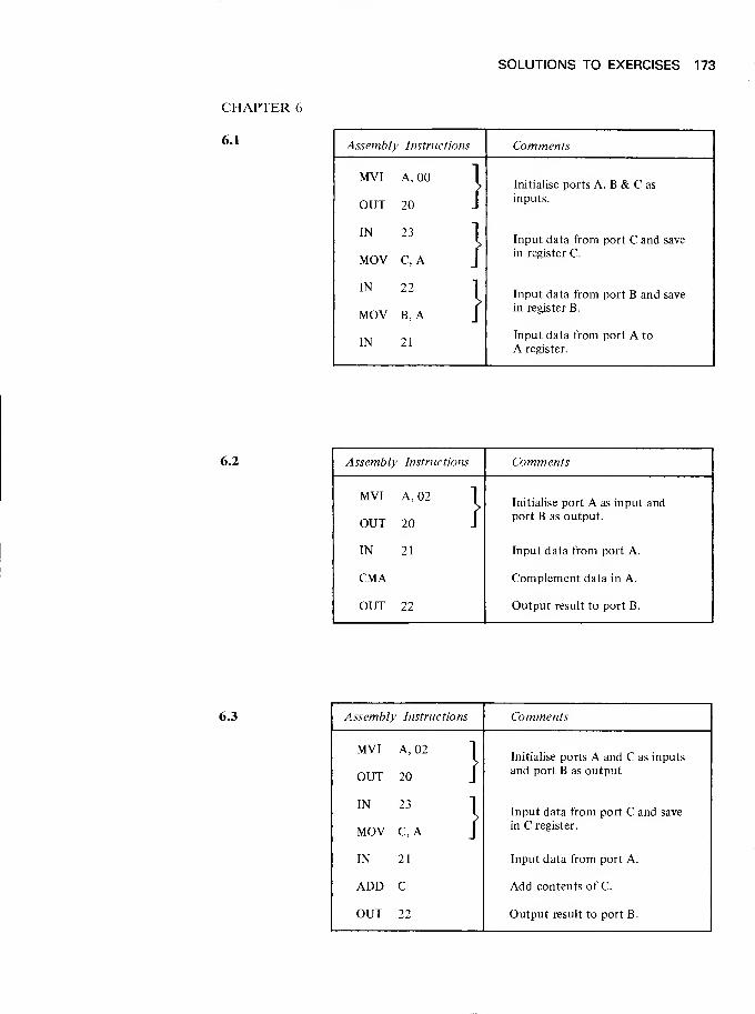
SOLUTIONS TO EXERCISES 173
CHAPTER 6
6.1 Assembly Instructions Comments
MVI A, 00 1Initialise ports A, B & C as
OUT 20 Jinputs.
IN
MOV
23"1
C, A J
Input data from port C and save
in register C.
IN
MOV
22 1
B, A J
Input data from port B and save
in register B
.
IN 21Input data from port A to
A register.
6.2 Assembly Instructions Comments
MVI A, 02 1
OUT 20 J
Initialise port A as input and
port B as output.
IN 21 Input data from port A.
CMA Complement data in A.
OUT 22 Output result to port B.
6.3 Assembly Instructions Comments
MVI A, 02 |
OUT 20 J
Initialise ports A and C as inputs
and port B as output
IN 23 1
MOV C, A J
Input data from port C and save
in C register.
IN 21 Input data from port A.
ADD C Add contents of C.
OUT 22 Output result to port B.

174 SOLUTIONS TO EXERCISES
CHAPTER 7
7.1
Triangular waveform:
FF-_-»
00
Assembly Instructions Comments
MVI
OUT
A, 02 1
20J
Initialise port B as an output port.
REPEAT: MVI A, 00 Initialise (A) to 00.
LABI: OUT 22 Output (A) to port B.
INR A Increment (A).
CPI
JNZ
00 1
LABI J
Loop if (A) have not overflowed to 00.
MVI A, FF Initialise (A) to FF.
LAB2: OUT 22 Output (A) to port B.
DCR A Decrement (A).
CPI
JNZ
FF 1
LAB2J
Loop if (A) have not underflowed to FF.
JMP REPEAT Repeat.
7.2 The following program reads a value from port A and uses this as a parameter
for a delay subroutine (see exercise 5.5). The computed delay is then used to
define the basic step duration for the DAC output and hence the rate of the
ramp waveform.
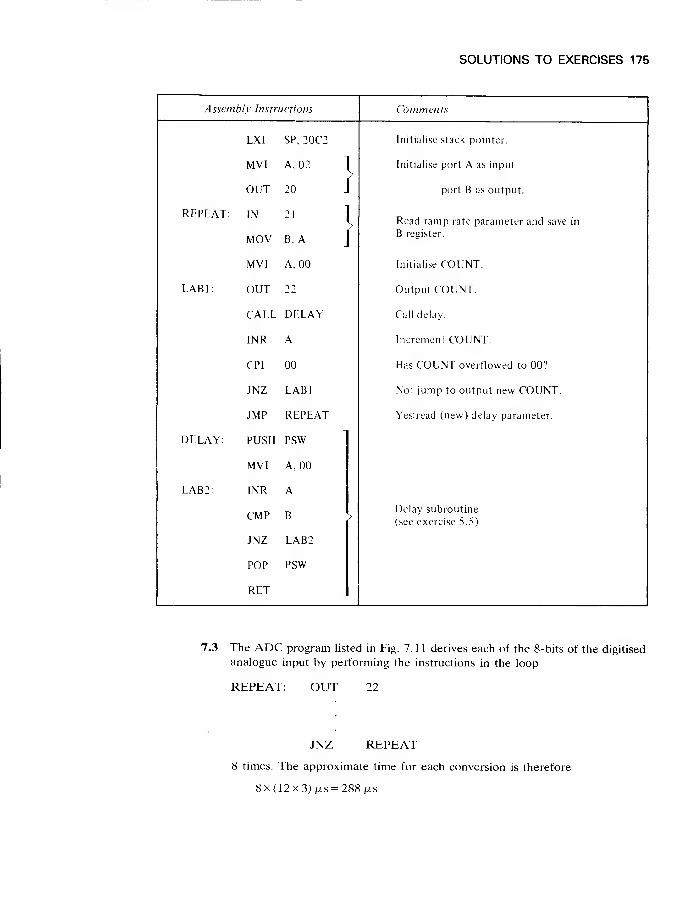
SOLUTIONS TO EXERCISES 175
Assembly Instructions Comments
LXI SP, 20C2 Initialise stack pointer.
MVI A, 02 1 Initialise port A as input
OUT 20 J port B as output.
REPEAT: IN 21
\Read ramp rate parameter and save in
MOV B, A JB register.
MVI A, 00 Initialise COUNT.
LABI: OUT 22 Output COUNT.
CALL DELAY Call delay.
INR A Increment COUNT.
CPI 00 Has COUNT overflowed to 00?
JNZ LABI No: jump to output new COUNT.
JMP REPEAT Yes: read (new) delay parameter.
DELAY: PUSH
MVI
PSW
A, 00
LAB2: INR A
CMP B >
Delay subroutine
(see exercise 5.5)
JNZ LAB2
POP PSW
RET
7.3 The ADC program listed in Fig. 7.11 derives each of the 8-bits of the digitised
analogue input by performing the instructions in the loop
REPEAT: OUT 22
JNZ REPEAT
8 times. The approximate time for each conversion is therefore
8x(12x3),u,s = 288/xs

7.4
176
Assembly Instructions Comments
LXI SP, 20C2 Initialise stack pointer.
LXI H, 2040 Initialise memory pointer.
MVI A, 02 1Initialise Port B as output.
OUT 20 J
Initialise
SegmentMVI
SIM
A, 08 1Reset interrupt mask bits.
MVI M, 00 Initialise ADC data.
MVI A, 01 "1
Initialise LED on.
STA 2041 J
" LOOP: El
MOV A, M 1
Enable interrupts.
MainProgram
> Compare ADC data with threshold value.
CPI THRES J
CP ALARM Conditional CALL to subrt ALARM.
JMP LOOP Continue
"ISR: PUSH PSW 1
PUSH B Save registers.
PUSH D J
Interrupt
Service <
CALL
MOV
ADC 1
M, A J
Perform A to D conversion store digitised
value in memory.
Routine
POP D1
POP B Restore registers.
POP PSW J
RET
ADC: iADCSubroutine
RET
1
>ADC subroutine.
" ALARM : LDA
OUT
2041:
22
LED indicator on L.S. bit of port B.
ALARM CALL DELAY Delay subroutine must provide a suitable
SubroutineCMP
STA
RET
A
2041
> on-off rate.

INDEXaccumulator 19
ADC - see Analogue to digital converter
ADD instruction 36
address
bus 13
decoder 16
memory 11
modes 21
aliasing 82
ALU -see Arithmetic logic unit
analogue multiplexers 86
analogue signal 79
analogue-to-digital converter 79-86,
121-22
AND instruction 46
arithmetic instructions 35
arithmetic logic unit 10
assembler 28, 130-31, 133
directives 132
assembly language 20, 28-30, 130
auxiliary carry flag 36, 44-46
Babbage, Charles 3
base 5
BCD -see Binary coded decimal
BCD arithmetic 44-46
bidirectional bus 14
binary system 5, 32-33
division 148
multiplication 145
binary coded decimal 32, 35
bits 5
BlU-see Bus interface unit
borrow in 38
borrow out 38
bus 10
interface unit 162
byte 6
call (instruction) 58
carry flag 36, 42
carry in 37
carry out 37
central processor unit 7
chip-select 15
chords 116
circular buffer 89
command byte 72
comparator 83
compare (instruction) 50
compiler 28, 132-33
condition bits 35
conditional jump instructions 53-54
conditional sequencing 103-106
control bus 13
conversion time 83
CPU - see Central processor unit
cross assembler 28
cross compiler 28
DAC - see Digital to analogue converter
data bus 13
data manipulation 21
data transfer 20
decrement 40, 42
instruction 40
define storage (assembler directive) 131
development system 129-30
digit 5
digital clock 106-13
digital input/output 72-74, 98-106
digital-to-analogue converter 79-80, 114
direct addressing 22-25
DI (instruction) 92
division (binary) 148-50
dual-ramp technique 83
EAROM 13
editor 130, 137
electrically alterable ROM 13
EI (instruction) 92
EPROM 11
EQUate (assembler directive) 131
erasable PROM 11
EU (execution unit) 162
event counter 158-59
examine register (monitor command)129
exclusive-OR (instruction) 48
execution cycle 7
execution unit 162
exponential waveform 117
extended addressing 22, 25
fetch cycle 7
flags register 19
177

178 INDEX
flowchart 54
hand coding 29
handshake control 70-78
hexadecimal code 6
high-level language 28
highway 10, 13
ICE 137
immediate addressing 22-24, 27, 38-40
IN (instruction) 69
in-circuit emulator 137
increment 39, 41
(instruction) 39, 41
index register 157
input port 7
instruction addressing mode 22
instruction set 28, 140
integrated circuit 1, 3
Intel 8085 18, 140-44
interface 7, 67
interpreters 130, 132, 134
interrupt 86-97
control registers 19
mask 92
priority level 93-95
service routine 88, 108
jump (instruction) 52-55
K 14
keypad 127
label 20, 59
large-scale integration 1
latched output 68
LED 68
light-emitting diode 68
locations (memory) 11
logical input 67
logical operations 46-50
machine control (instructions) 21
machine instructions 4-7, 18-21, 28
macros (assembler) 131
MDS 129-30
medium-scale integration 1
memory 7, 11
memory map 15, 16
memory mapped input/output 69
memory transfer (instructions) 10
microcomputer 7
microprocessor 1-7
8-bit 156-58
16-bit 156, 158-60
monitor (program) 28, 127
commands 128
Motorola 6800/9 158, 159
multiple interrupts 91
multiplication (binary) 145-55
multiprecision arithmetic 41-43
multiprecision instructions 41
nested subroutines 64-66
nibbles 162
non-volatile 11
numeric display 127
object code 28
operation mnemonic 20
OR (instruction) 48
origin address (assembler directive) 132
OUT (instruction) 69-72
parameter 62
parameter passing 62
parity flag 48
partial product 145
peripheral 79
piecewise linearisation 114
piecewise linear interpolation 116-20
PI/O 68-78
POP (instruction) 62
ports 7, 68, 71
process controller 121
program 4
program counter 7
programmable input/output device 68-
78
programmable timer 108
programmed input/output 69
PROM programmer 13, 130
pseudo-ops 132
PUSH (instruction) 62
RAM 11, 15
random access memory 11, 15
RIM (instruction) 93
read only memory 11, 15
real-time clock 86, 106
trace 137
register 10
addressing 22-24, 37-39
indirect addressing 22, 26-27, 38-40

INDEX 179
relative jump (instruction) 158
reset (monitor command) 128
resident operating program 28RETurn (instruction) 58
ROM 11, 15
rotate (instruction) 49
run (monitor command) 128
sample and hold (circuits) 86sampling time 82
sequencing 98-106
SIM (instruction) 93
seven-segment (LED) display 110
Shannon sampling theorem 81
sign and magnitude 33
flag 36
single board system 126
single chip (microcomputer) 158-60
single step (monitor command) 129
small-scale integration 1
source code 28
stack 59, 62
operations 62
pointer register 19
status bits 35
stored program (concept) 4
string 163
subroutine 55-59
substitute memory (monitor command)128
SUBtract (instruction) 38
successive approximation (ADC) 83-85
symbolic assembly language 28-30, 130
symbolic name, 59, 131
system programs 28, 129
table look-up 114
target system 137
temperature control system 5, 121-25
Texas 9900 160
three-state output 14
timer (programmable) 108
timing and control (section) 10
signals 16
traffic light sequences 99-102
transfer of control 21, 52-54
transistor 13
TRAP (interrupt) 92-93
truth table 37-38
two's complement 33-34
unconditional jump (instruction) 52
UV EPROM 13
vector address 91
volatile 11
washing machine controller 103-106
waveform generation 114
word (computer) 6
XOR (instruction) 8
zero flag 36
Zilog Z80 46, 157
Z8000 162

oThis is a basic introductory text on microprocessors and their ^applications which assumes little previous knowledge of them. The qessential characteristics of microprocessors and their operating and ^application principles are given with the minimum of fl)
electrical /electronic detail. This means that a broad spectrum of CAengineers and professional people, from many different JCbackgrounds, can see the relevance of microprocessors to their Sspeciality and confidently begin the process of selecting a system __and applying it, without becoming entangled in the technology. 2?
3Students in technical colleges, polytechnics and universities will find 3the approach particularly suitable. Although the book stands on its ijown , the many program and application examples can be run
directly on a microprocessor prototyping system, and the book is 3therefore eminently suited to any hands-on introductory course. <D
3The chapter on Applications covers all baste types of application with fff"
relatively simple examples, and the chapter on Development Aids is a £1guide to setting up a system. *"
ISBN 273 01522 2
X
s
Pitman ^net in U.K. «"M
£7-5P g