The Evolution of Multi-Chip Packaging: from MCMs …meptec.org/Resources/9 - McCann.pdfOutline •...
33
The Evolution of Multi-Chip Packaging: from MCMs to 2.5/3D to Photonics David McCann November 14, 2016
-
Upload
truongnguyet -
Category
Documents
-
view
225 -
download
1
Transcript of The Evolution of Multi-Chip Packaging: from MCMs …meptec.org/Resources/9 - McCann.pdfOutline •...
The Evolution of Multi-Chip Packaging: from MCMs to 2.5/3D to Photonics
David McCann
November 14, 2016
Outline
• Multi-Chip Module Evolution
• We had MCM’s. What Happened? What Have we Learned?
• Trends and Drivers of Packaging
• Memory’s Role
• Enabling Technologies for MCM Applications
• How to Meet Business Requirements?
• “The Future”
• Summary
2
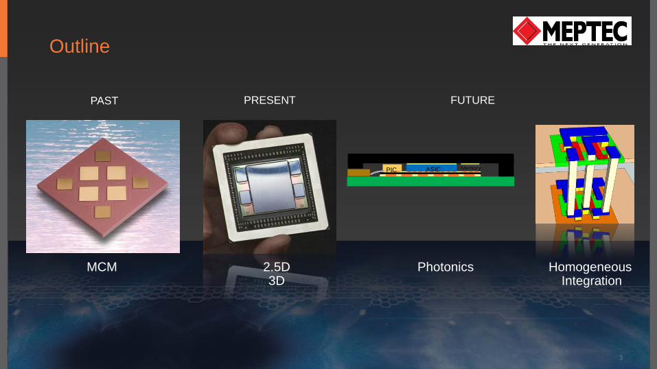
Outline
3
PAST PRESENT FUTURE
ASIC Memory
Lid
PIC
2.5D 3D
MCM Photonics Homogeneous Integration
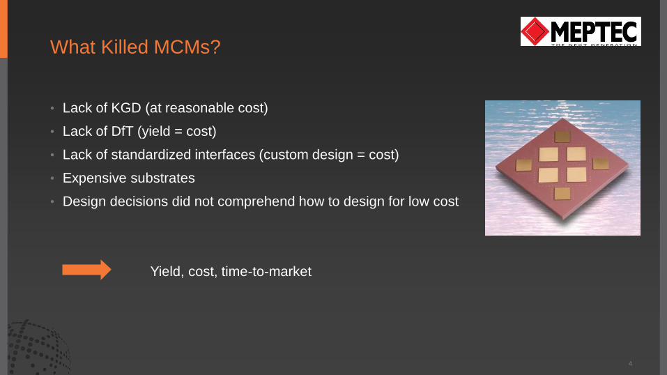
What Killed MCMs?
• Lack of KGD (at reasonable cost)
• Lack of DfT (yield = cost)
• Lack of standardized interfaces (custom design = cost)
• Expensive substrates
• Design decisions did not comprehend how to design for low cost
Yield, cost, time-to-market
4
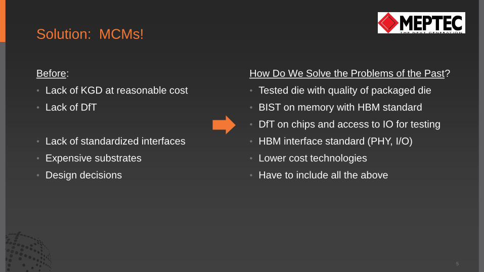
Solution: MCMs!
Before:
• Lack of KGD at reasonable cost
• Lack of DfT
• Lack of standardized interfaces
• Expensive substrates
• Design decisions
How Do We Solve the Problems of the Past?
• Tested die with quality of packaged die
• BIST on memory with HBM standard
• DfT on chips and access to IO for testing
• HBM interface standard (PHY, I/O)
• Lower cost technologies
• Have to include all the above
5

Mega Trends Drivers of MCMs
6
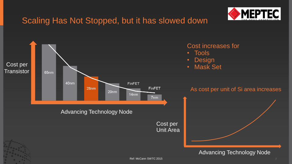
Scaling Has Not Stopped, but it has slowed down
7 Ref: McCann SWTC 2015
Cost increases for • Tools • Design • Mask Set
Advancing Technology Node
Cost per Unit Area
Advancing Technology Node
Cost per
Transistor
As cost per unit of Si area increases
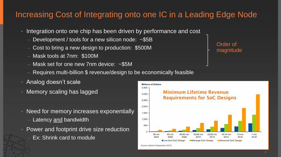
Increasing Cost of Integrating onto one IC in a Leading Edge Node
• Integration onto one chip has been driven by performance and cost
– Development / tools for a new silicon node: ~$5B
– Cost to bring a new design to production: $500M
– Mask tools at 7nm: $100M
– Mask set for one new 7nm device: ~$5M
– Requires multi-billion $ revenue/design to be economically feasible
• Analog doesn’t scale
• Memory scaling has lagged
• Need for memory increases exponentially
– Latency and bandwidth
• Power and footprint drive size reduction
– Ex: Shrink card to module
8
Order of magnitude
Minimum Lifetime Revenue
Requirements for SoC Designs
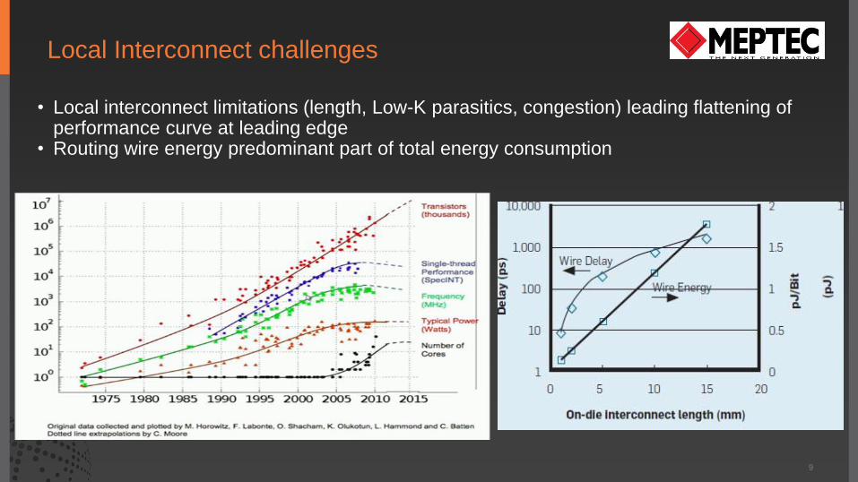
Local Interconnect challenges
• Local interconnect limitations (length, Low-K parasitics, congestion) leading flattening of performance curve at leading edge
• Routing wire energy predominant part of total energy consumption
9
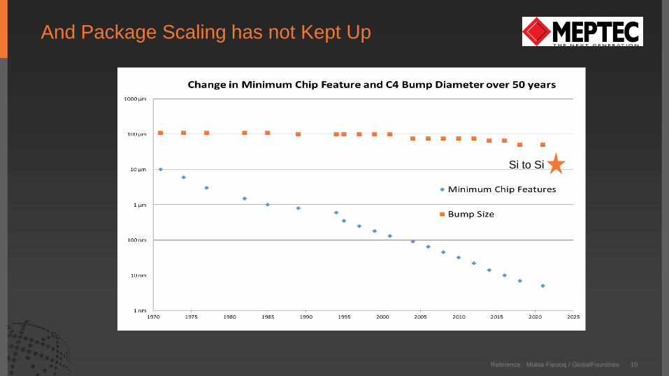
And Package Scaling has not Kept Up
Reference: Mukta Farooq / GlobalFoundries 10
Si to Si
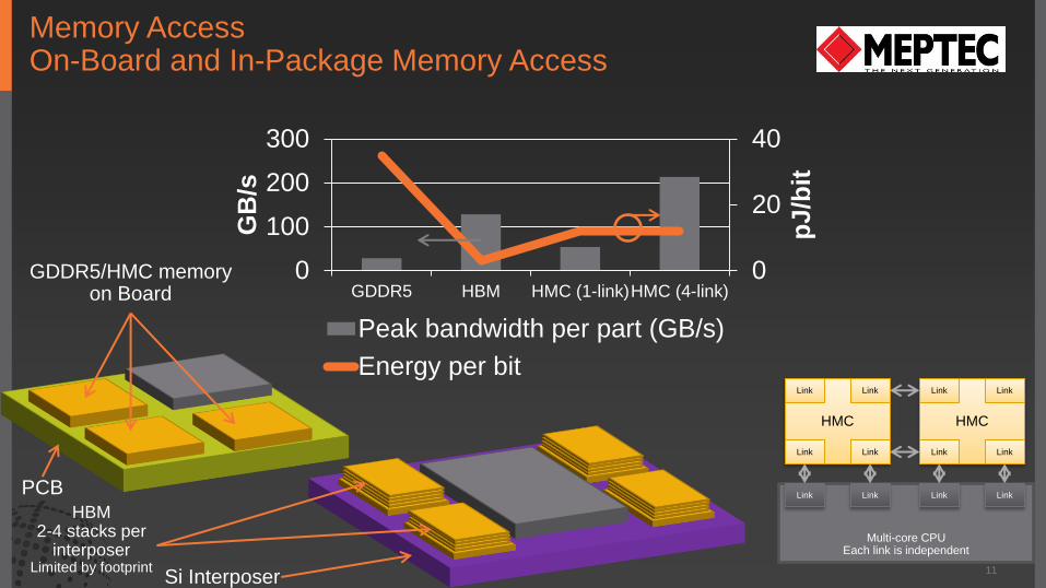
Memory Access On-Board and In-Package Memory Access
HMC
Link Link
Link Link
HMC
Link Link
Link Link
Multi-core CPU Each link is independent
Link Link Link Link
0
20
40
0
100
200
300
GDDR5 HBM HMC (1-link)HMC (4-link)
pJ/b
it
GB
/s
Peak bandwidth per part (GB/s)
Energy per bit
GDDR5/HMC memory on Board
PCB
Si Interposer
HBM 2-4 stacks per
interposer Limited by footprint 11
Memory Trends
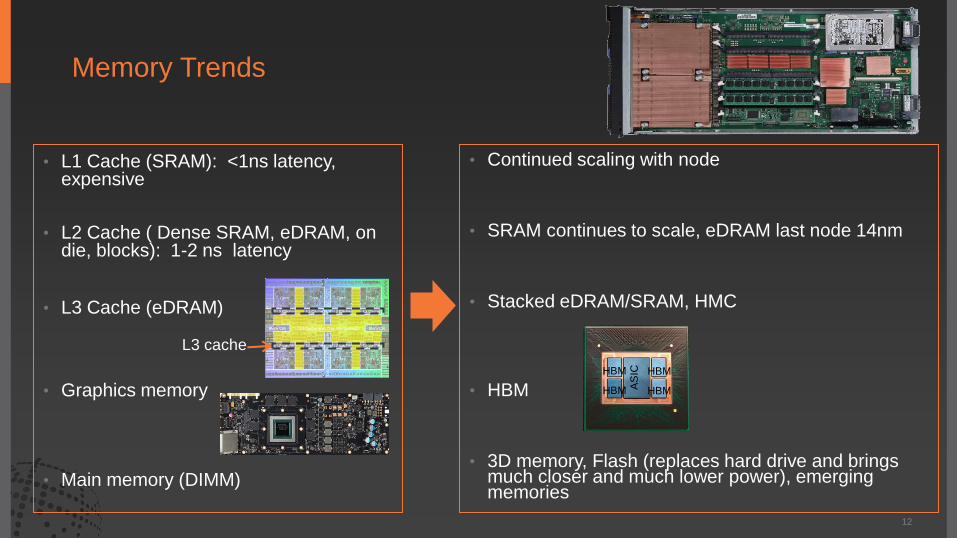
• L1 Cache (SRAM): <1ns latency, expensive
• L2 Cache ( Dense SRAM, eDRAM, on die, blocks): 1-2 ns latency
• L3 Cache (eDRAM)
• Graphics memory
• Main memory (DIMM)
12
• Continued scaling with node
• SRAM continues to scale, eDRAM last node 14nm
• Stacked eDRAM/SRAM, HMC
• HBM
• 3D memory, Flash (replaces hard drive and brings
much closer and much lower power), emerging memories
L3 cache
AS
IC
HBM
HBM
HBM
HBM
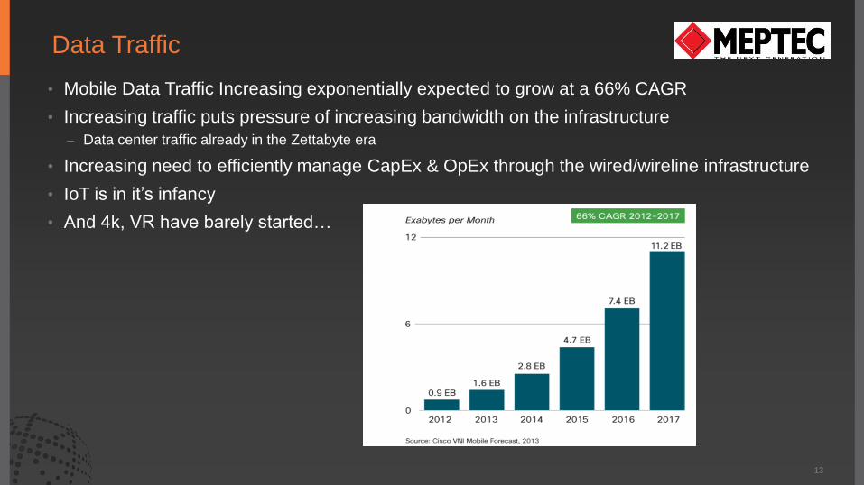
Data Traffic
• Mobile Data Traffic Increasing exponentially expected to grow at a 66% CAGR
• Increasing traffic puts pressure of increasing bandwidth on the infrastructure
– Data center traffic already in the Zettabyte era
• Increasing need to efficiently manage CapEx & OpEx through the wired/wireline infrastructure
• IoT is in it’s infancy
• And 4k, VR have barely started…
13
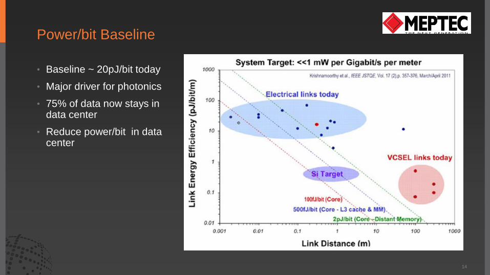
Power/bit Baseline
• Baseline ~ 20pJ/bit today
• Major driver for photonics
• 75% of data now stays in data center
• Reduce power/bit in data center
14
Enabling Technologies for MCM Applications
15
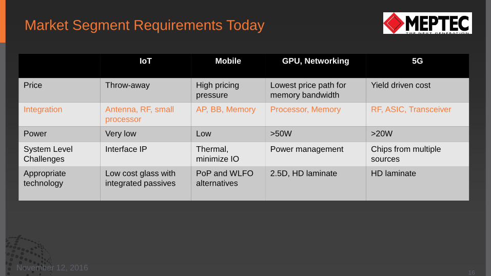
Market Segment Requirements Today
16
November 12, 2016
IoT Mobile GPU, Networking 5G
Price Throw-away High pricing
pressure
Lowest price path for
memory bandwidth
Yield driven cost
Integration Antenna, RF, small
processor
AP, BB, Memory Processor, Memory RF, ASIC, Transceiver
Power Very low Low >50W >20W
System Level
Challenges
Interface IP Thermal,
minimize IO
Power management Chips from multiple
sources
Appropriate
technology
Low cost glass with
integrated passives
PoP and WLFO
alternatives
2.5D, HD laminate HD laminate
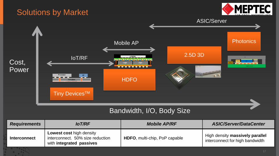
Solutions by Market
17
GLOBALFOUNDRIES Confidential 17
Cost, Power
Tiny DevicesTM
HDFO
2.5D 3D
Mobile AP
ASIC/Server
IoT/RF
Bandwidth, I/O, Body Size
Requirements IoT/RF Mobile AP/RF ASIC/Server/DataCenter
Interconnect
Lowest cost high density
interconnect. 50% size reduction
with integrated passives
HDFO, multi-chip, PoP capable High density massively parallel
interconnect for high bandwidth
Photonics
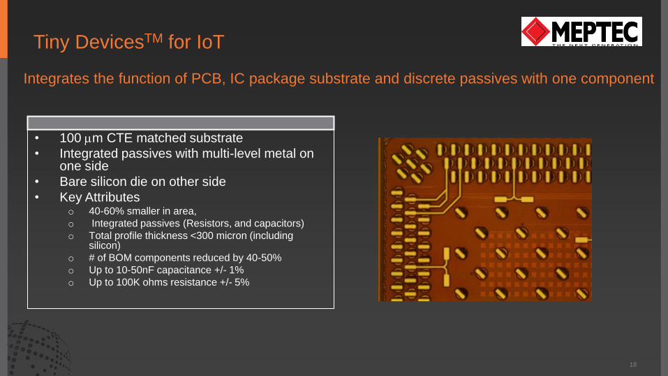
18
• 100 mm CTE matched substrate
• Integrated passives with multi-level metal on one side
• Bare silicon die on other side
• Key Attributes o 40-60% smaller in area,
o Integrated passives (Resistors, and capacitors)
o Total profile thickness <300 micron (including silicon)
o # of BOM components reduced by 40-50%
o Up to 10-50nF capacitance +/- 1%
o Up to 100K ohms resistance +/- 5%
Tiny DevicesTM for IoT
Integrates the function of PCB, IC package substrate and discrete passives with one component
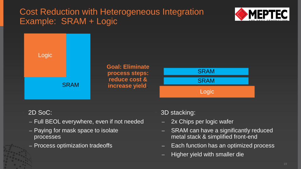
Cost Reduction with Heterogeneous Integration Example: SRAM + Logic
• 2D SoC:
– Full BEOL everywhere, even if not needed
– Paying for mask space to isolate processes
– Process optimization tradeoffs
• 3D stacking:
– 2x Chips per logic wafer
– SRAM can have a significantly reduced metal stack & simplified front-end
– Each function has an optimized process
– Higher yield with smaller die
19
SRAM
Logic
Logic
SRAM
SRAM Goal: Eliminate process steps: reduce cost & increase yield.
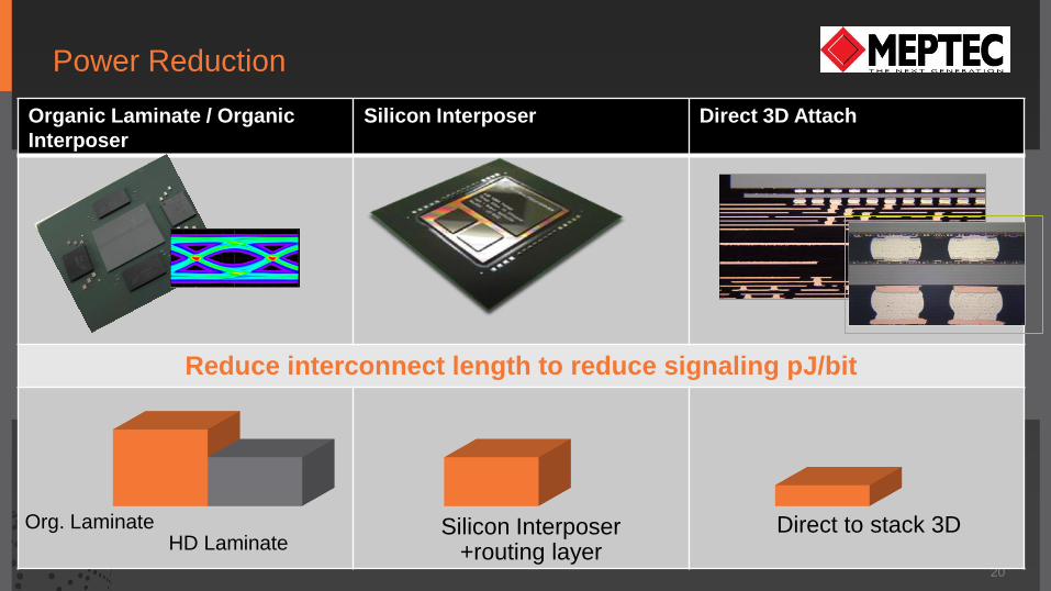
Power Reduction
20
Organic Laminate / Organic
Interposer
Silicon Interposer Direct 3D Attach
Reduce interconnect length to reduce signaling pJ/bit
Direct to stack 3D Silicon Interposer +routing layer
Org. Laminate HD Laminate
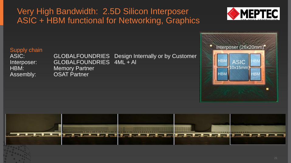
Very High Bandwidth: 2.5D Silicon Interposer ASIC + HBM functional for Networking, Graphics
21
Supply chain ASIC: GLOBALFOUNDRIES Design Internally or by Customer Interposer: GLOBALFOUNDRIES 4ML + Al HBM: Memory Partner Assembly: OSAT Partner
Interposer (26x20mm)
ASIC (10x15mm)
HBM
HBM
HBM
HBM
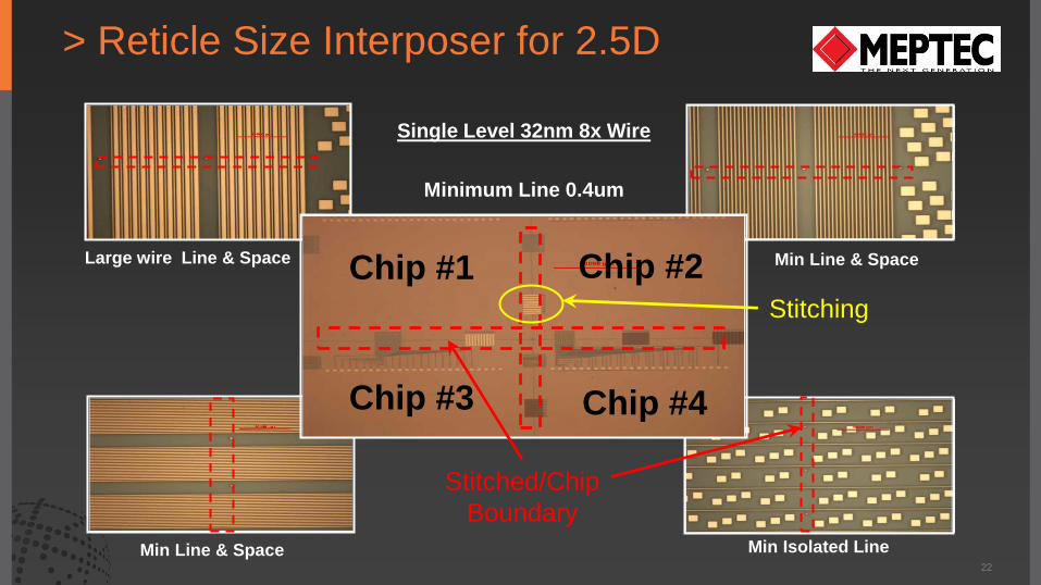
Chip #4
Chip #2
Chip #3
Chip #1
Single Level 32nm 8x Wire
Minimum Line 0.4um
Stitched/Chip
Boundary
Min Line & Space Min Isolated Line
Large wire Line & Space Min Line & Space
Stitching
Chip #4
22
> Reticle Size Interposer for 2.5D
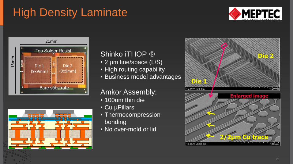
High Density Laminate
Shinko iTHOP ® • 2 µm line/space (L/S)
• High routing capability
• Business model advantages
Amkor Assembly: • 100um thin die
• Cu µPillars
• Thermocompression
bonding
• No over-mold or lid
Die 1
Die 2
Enlarged image
2/2µm Cu trace
23
24
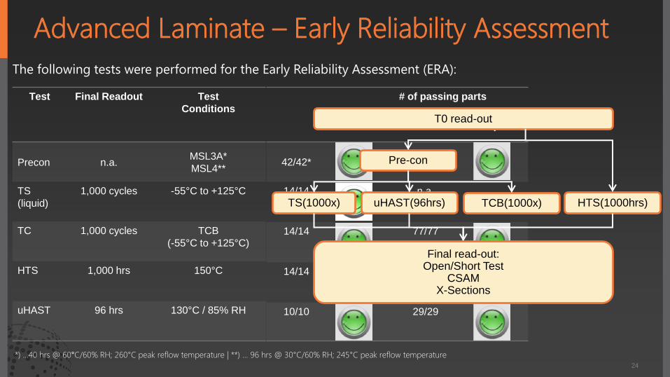
Advanced Laminate – Early Reliability Assessment
The following tests were performed for the Early Reliability Assessment (ERA):
Test Final Readout
Test
Conditions
Precon n.a. MSL3A*
MSL4**
TS
(liquid)
1,000 cycles -55°C to +125°C
TC 1,000 cycles TCB
(-55°C to +125°C)
HTS 1,000 hrs 150°C
uHAST 96 hrs 130°C / 85% RH
# of passing parts
SHINKO Assy/ AMKOR Assy/
SHINKO test dies GF top dies
42/42* 143/143**
14/14 n.a.
14/14 77/77
14/14 29/29
10/10 29/29
*) …40 hrs @ 60°C/60% RH; 260°C peak reflow temperature | **) … 96 hrs @ 30°C/60% RH; 245°C peak reflow temperature
T0 read-out
Pre-con
TCB(1000x) uHAST(96hrs) HTS(1000hrs) TS(1000x)
Final read-out: Open/Short Test
CSAM X-Sections
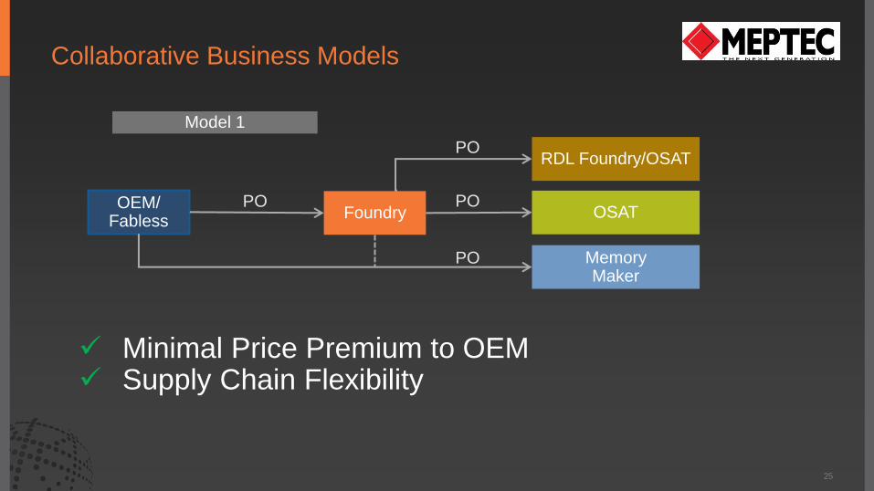
Collaborative Business Models
OEM/ Fabless
Foundry
Memory Maker
OSAT PO
PO
RDL Foundry/OSAT
PO
PO
Minimal Price Premium to OEM Supply Chain Flexibility
Model 1
25
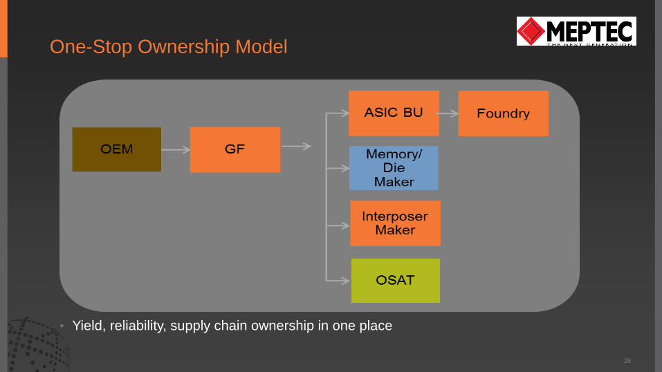
One-Stop Ownership Model
• Yield, reliability, supply chain ownership in one place
26
Test
• The Industry must agree on Known-Good Die definition – and then deliver – KGD = “deliver the same quality level as package die” (get this accepted as standard)
• The problem is often not “Test” – but “Yield management” – We know how to thoroughly test all circuits/components. The testing must be done at wafer
level or the yield loss (cost) will be unaffordable
• There are not industry-wide standards for Design-for-Test for multi-chip products
and processes for supplying test details from components suppliers to multi-chip
integrators – There are not standards for what needs to be tested at module test
– JEDEC standards for HBM are a major advancement
– Some test methods may be proprietary – will all suppliers share them ?
• Additional DFT is needed for multi-chip Testing – that is not always supplied today (KGD) – All chips must have boundary scan for interconnect testing
– It must be possible to apply all required tests at final package level. All IOs may not be accessible
– IC suppliers must ensure their part is still testable
27

The Future (Coming to you Soon…)
28
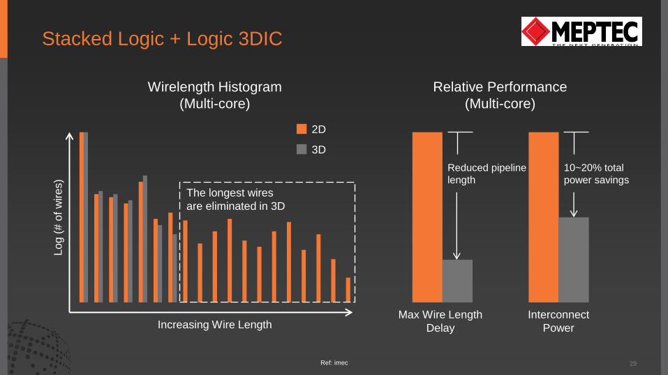
Stacked Logic + Logic 3DIC
29
Relative Performance
(Multi-core)
Reduced pipeline
length
10~20% total
power savings
Max Wire Length
Delay
Interconnect
Power
Wirelength Histogram
(Multi-core)
The longest wires
are eliminated in 3D
Lo
g (
# o
f w
ire
s)
Increasing Wire Length
2D
3D
Ref: imec
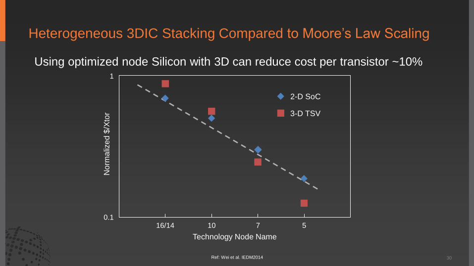
Heterogeneous 3DIC Stacking Compared to Moore’s Law Scaling
30
16/14
Technology Node Name
Norm
aliz
ed
$/X
tor
10 7 5 0.1
1
2-D SoC
3-D TSV
Using optimized node Silicon with 3D can reduce cost per transistor ~10%
Ref: Wei et al. IEDM2014
Die Partitioning Benefits
• Study of partitioning 8mm x 9mm single logic die into 2ea 6mm x 6mm logic die
• Smaller die results in better yield, $ savings
• Stacking enables lower power with shorter interconnect, system level $ savings
– Power savings higher with stacks with memory (more repeaters)
• Balance against memory architecture complexity increase and added $ cost of TSV and assembly
31
TSV 3D based
• UltraSparc uP
• 2-layer stack, 28nm
• Logic/Logic
• Footprint -47% and Power -17%
• 1800TSVs/mm2
Ref: Georgia Tech
Cost of package using 3D TSV
Standard wafer processing
TSV processing
Area lost to TSV
Extra packaging cost
Summary
• MCM’s were driven by performance in the 1990’s, but struggled due to yield and cost
• Megatrends are again driving MCM’s in every market
• These Megatrends include the cost of continued scaling, rapidly increasing data, the need for much higher memory bandwidth and reduced latency, pervasive IoT, and power / bit reduction
• Yield, Cost, and TTM are required for success of future MCMs
• Yield and TTM will be addressed by DfT and test standards at wafer level and what to test at module level
• Cost will be addressed by yield, by utilizing devices from best-cost-for-application nodes, and by development of new lower cost technologies like Tiny DevicesTM and 2.1D for MCMs
• 3D stacking will be required for maximum interconnect density
32
Trademark Attribution
GLOBALFOUNDRIES®, the GLOBALFOUNDRIES logo and combinations thereof, and GLOBALFOUNDRIES’ other trademarks and service marks are owned by GLOBALFOUNDRIES Inc. in the United States and/or other jurisdictions. All other brand names, product names, or trademarks belong to their respective owners and are used herein solely to identify the products and/or services offered by those trademark owners.
© 2015 GLOBALFOUNDRIES Inc. All rights reserved.
Thank You
33
Appreciation for support on this presentation to: Phil Nigh Rama Alapati Dan Berger Jean Trewhella Mukta Farooq
Subramanian Iyer Adam Beece Saket Chadda Jeannette Koernert