THE EMERGENCE OF PLASMA PROCESSING
23
University of California, Berkeley PLASMA THE EMERGENCE OF PLASMA PROCESSING M.A. Lieberman Department of Electrical Engineering and Computer Sciences University of California Berkeley, CA 94720 References: H. Abe, M. Yoneda and N. Fujiwara, Jpn. J. Appl. Phys. 47, 1435 (2008) V.M. Donnelly and A. Kornblit, J. Vac. Sci. Technol. A31, 050825 (2013) Special thanks to: John W. Coburn Download this talk: http://www.eecs.berkeley.edu/∼lieber LiebermanGEC10 1
Transcript of THE EMERGENCE OF PLASMA PROCESSING

University of California, Berkeley PLASMA
THE EMERGENCE OF PLASMA PROCESSING
M.A. Lieberman
Department of Electrical Engineering and Computer SciencesUniversity of California
Berkeley, CA 94720
References:H. Abe, M. Yoneda and N. Fujiwara, Jpn. J. Appl. Phys. 47, 1435 (2008)
V.M. Donnelly and A. Kornblit, J. Vac. Sci. Technol. A31, 050825 (2013)
Special thanks to: John W. Coburn
Download this talk:
http://www.eecs.berkeley.edu/∼lieber
LiebermanGEC10 1

University of California, Berkeley PLASMA
OUTLINE
• The nanoelectronics revolution
• The emergence of plasma processing
• The evolution of etching discharges
• Future etch challenges
LiebermanGEC10 2

University of California, Berkeley PLASMA
THE NANOELECTRONICS REVOLUTION
• Transistors/chip doubling every 11
2–2 years since 1959
• Billion-fold increase in performance for the same costover the last 40 years
EQUIVALENT AUTOMOTIVE ADVANCE
• 60 billion miles/hr (90 × speed of light!)
• 20 billion miles/gal
• 1 cm long × 3 mm wide
LiebermanGEC10 3

University of California, Berkeley PLASMA
EMERGENCE OF PLASMA PROCESSING
LiebermanGEC10 4

University of California, Berkeley PLASMA
HUMBLE BEGINNINGS — SILVERING MIRRORS
• Sputtering discovered bySir William Grove in 1852
• Relative sputtering ratesof various metals measuredin 1890–1910
• Crude apparatus used tosputter-coat silver, plat-inum, etc on glass sur-faces
• The mechanism of phys-ical sputtering was notunderstood
• Discharge state-of-the-artin the 1920’s was rudi-mentary
10. " NOTE ON THE PRODUCTION OF MIRRORS BY CATHODIC
BOMBARDMENT"
By F. SIMEON, B.SC., F.lnst.P.
(Messrs. Adam Hilger, Ltd.)
The production of mirrors by cathodic bombardment is not a new process.Workers with vacuum tubes since Grove, 1852, have noticed the bright deposit inthe neighbourhood of platinum electrodes, which is more or less marked according tothe current passed through the tube and nature of the residual gas. This deposit
is generally objectionable, and was especially so in the case of the older form of X-raybulb with platinum anti-cathode. This disintegration is not peculiar to platinum, norindeed is platinum the most easily deposited metal. Sir William Crookes in 1891investigated the relative rates of sputtering of a number of different metals undersimilar conditions of discharge. The relative rates are given in the following table,in which the rate for gold is taken as 100*
Palladium 108·80 Platinum 44·0 Iridium 10·49Gold 100·00 Copper 40·24 Iron 5·50Silver ... 82·68 Cadmium 31·99 Aluminium 0·0
Lead ... 75·04 Nickel 10·99 Magnesium 0·0Tin... 56·96
Many other observers both before and since have investigated various pointshaving some bearing upon this method. A bibliography of their papers will be foundin the reference given.
A convenient apparatus consists of a vacuum tube of special form which permitsof readily altering the cathode and of introducing and removing the various objects(glass plates, &c.) which it is desired to coat with a reflecting surface. The vesselemployed in the apparatus exhibited is a vacuum dessicator, through the upper partof which is introduced, in addition to the exhaust tube for connection to the vacuumpump, two aluminium wires covered with glass tubing for insulation. To one ofthese, which is introduced centrally, can be attached a disc of the fine metal of whichit is desired to form a mirror. The other, after emerging from the glass tube, is bentinto a portion of a circle, in about the same horizontal plane as the surface to be coated,and so as to be as far removed from the surface as the vessel allows. These wires areconnected externally to an induction coil, a Lodge valve also being included in thecircuit. The article to be coated, after being scrupulously cleaned and dried,is
placed upon a clean glass support in the lower part of the vessel. Connectionbetween the two parts of the vessel is made with some form of vacuum grease, greatcare being exercised that neither the surface to be coated nor the cathode itself is inany way contaminated, as this will lead to some blemish in the final result. Thevessel is exhausted until the cathode dark space
(From “The Making of Reflecting Surfaces”, Phys. Soc., London, 26 Nov 1920)
LiebermanGEC10 5

University of California, Berkeley PLASMA
INVENTION OF THE TRANSISTOR — 1948
W.B. Shockley,J. Bardeen,W.H. Brattain
Nobel Prize in Physics(1956)
LiebermanGEC10 6

University of California, Berkeley PLASMA
FIRST INTEGRATED CIRCUIT AND MICROPROCESSOR
Jack Kilby (1958)
Nobel Prize in Physics (2000)
Texas Instruments TMS 1000
USP 3,757,306 (1973)
LiebermanGEC10 7

University of California, Berkeley PLASMA
SPUTTER DISCHARGE STATE-OF-THE-ART — 1960’s
• Parallel plate capacitively coupled rf discharges that generatedenergetic ions were widely used for sputter-etching andsputter-deposition
• Formation of the ion energy distribution on substrate surface
• Role of blocking capacitor and formation of self-bias voltage
• Influence of electrode area ratio on dc plasma potential
• Optical emission spectroscopy for etch end-point detection
• Reactive sputter deposition
• Basic theory of physical sputtering
LiebermanGEC10 8

University of California, Berkeley PLASMA
EXAMPLES
• Earliest measurement of ion energy distribution (J. Ero, 1958)
• Blocking capacitor and self-bias voltage (Butler andKino, 1963)
LiebermanGEC10 9

University of California, Berkeley PLASMA
PLASMA ETCH STATE-OF-THE-ART — 1970’s
• Etch was isotropic
• Capacitively-powered “barrel” etchers were mainly used
• High pressures (∼ 1 Torr)
• An important application was photoresist strip
• Isotropic etching of Si, W, Ta, Ti, Si3N4 was demonstrated
• Need for volatile etch products was recognized
• No mention of energetic ion bombardment
LiebermanGEC10 10

University of California, Berkeley PLASMA
ION-ENHANCED PLASMA ETCHING
• Sputtering — involatile products and high ion energies
• Plasma etching — volatile products and low ion energies
Who first combined volatile products with high ion energies?
N. Hosokawa, R. Matsuzake and T. Asamaki
“RF Sputter-Etching by Fluoro-Chloro-Hydrocarbon Gases”
Jpn. J. Appl. Phys. Suppl. 2, Pt. 1, 435 (1974)
LiebermanGEC10 11
University of California, Berkeley PLASMA
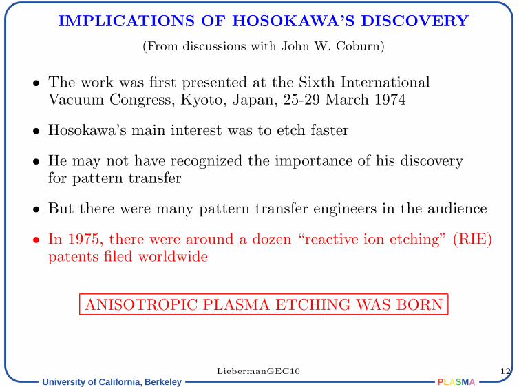
IMPLICATIONS OF HOSOKAWA’S DISCOVERY
(From discussions with John W. Coburn)
• The work was first presented at the Sixth InternationalVacuum Congress, Kyoto, Japan, 25-29 March 1974
• Hosokawa’s main interest was to etch faster
• He may not have recognized the importance of his discoveryfor pattern transfer
• But there were many pattern transfer engineers in the audience
• In 1975, there were around a dozen “reactive ion etching” (RIE)patents filed worldwide
ANISOTROPIC PLASMA ETCHING WAS BORN
LiebermanGEC10 12
University of California, Berkeley PLASMA
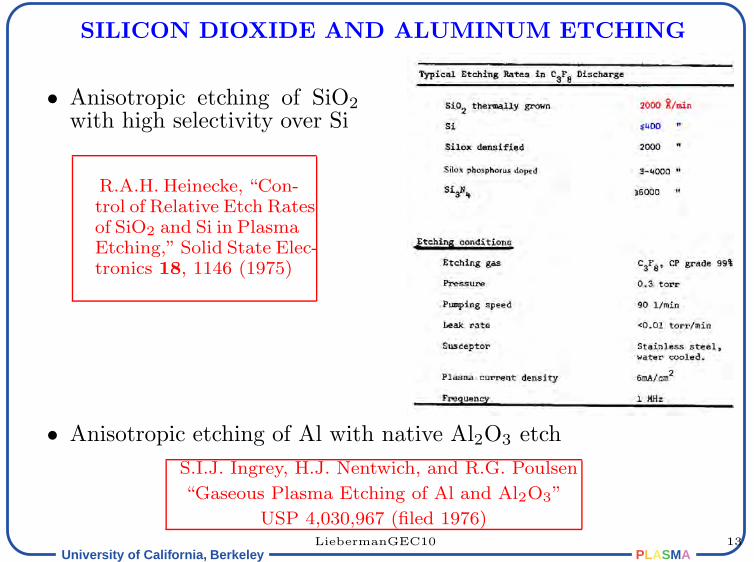
SILICON DIOXIDE AND ALUMINUM ETCHING
• Anisotropic etching of SiO2
with high selectivity over Si
R.A.H. Heinecke, “Con-trol of Relative Etch Ratesof SiO2 and Si in PlasmaEtching,” Solid State Elec-tronics 18, 1146 (1975)
• Anisotropic etching of Al with native Al2O3 etch
S.I.J. Ingrey, H.J. Nentwich, and R.G. Poulsen
“Gaseous Plasma Etching of Al and Al2O3”
USP 4,030,967 (filed 1976)LiebermanGEC10 13

University of California, Berkeley PLASMA
EVOLUTION OF ETCHING DISCHARGES
LiebermanGEC10 14

University of California, Berkeley PLASMA
THREE GENERATIONS OF ETCHING DISCHARGES
FIRST GEN-ERATION(1 source,multi-wafer,low density)
SECONDGENER-ATION(2 sources,single wafer,high density)
THIRD GEN-ERATION(multi-source,single wafer,moderate density)
LiebermanGEC10 15

University of California, Berkeley PLASMA
HIGH DENSITY INDUCTIVE DISCHARGES
LiebermanGEC10 16

University of California, Berkeley PLASMA
MOTIVATION
• High density (compared to capacitive discharge)
• Independent control of plasma density and ion energy
• Simplicity of concept
• RF rather than microwave powered
• No source magnetic fields
LiebermanGEC10 17

University of California, Berkeley PLASMA
EARLY HISTORY
• First inductive discharge by Hittorf (1884)
• Arrangement to test discharge mechanism by Lehmann (1892)
LiebermanGEC10 18

University of California, Berkeley PLASMA
CYLINDRICAL AND PLANAR CONFIGURATIONS
• Cylindrical coil
• Planar coil
LiebermanGEC10 19

University of California, Berkeley PLASMA
MICROWAVE DISCHARGES, PULSING,
AND ELECTRONEGATIVE GASES
LiebermanGEC10 20

University of California, Berkeley PLASMA
HIGH DENSITY PULSED MICROWAVE DISCHARGE
LiebermanGEC10 21

University of California, Berkeley PLASMA
ELECTRONEGATIVE DISCHARGES (Ar/H2S, O2)
• Attaching gases soak up electrons fast
LiebermanGEC10 22

University of California, Berkeley PLASMA
FUTURE ETCH CHALLENGES
• New materials and structures
• For 10 nm CD, must control accuracy to ±1 nm(1.8 lattice constants!) across 450 mm wafer
⇒ Gentle and precise etches
RESPONSES
• Evolutionary: more “knobs” on “existing” tools— Multiple driving frequencies/dc/magnetic fields etc— Segmented electrodes/driving coils/chucks etc— Many pulsing duty cycles, frequencies etc
⇒ Tight control of electron, ion and photonenergy distributions and fluxes
• Revolutionary: atomic layer etching and neutral beam etching
Download this talk:
http://www.eecs.berkeley.edu/∼lieber
LiebermanGEC10 23