THE DESIGN OF A HIGH FREQUENCY PULSE WIDTH MODULATION...
117
THE DESIGN OF A HIGH FREQUENCY PULSE WIDTH MODULATION INTEGRATED CIRCUIT WITH EXTERNAL SYNCHRONIZATION CAPABILITY A THESIS SUBMITTED TO THE GRADUATE SCHOOL OF NATURAL AND APPLIED SCIENCES OF MIDDLE EAST TECHNICAL UNIVERSITY BY OSMAN ULAŞ ŞAHİN IN PARTIAL FULFILLMENT OF THE REQUIREMENTS FOR THE DEGREE OF MASTER OF SCIENCE IN ELECTRICAL AND ELECTRONICS ENGINEERING FEBRUARY 2017
Transcript of THE DESIGN OF A HIGH FREQUENCY PULSE WIDTH MODULATION...

THE DESIGN OF A HIGH FREQUENCY PULSE WIDTH MODULATION
INTEGRATED CIRCUIT WITH EXTERNAL SYNCHRONIZATION
CAPABILITY
A THESIS SUBMITTED TO
THE GRADUATE SCHOOL OF NATURAL AND APPLIED SCIENCES
OF
MIDDLE EAST TECHNICAL UNIVERSITY
BY
OSMAN ULAŞ ŞAHİN
IN PARTIAL FULFILLMENT OF THE REQUIREMENTS
FOR
THE DEGREE OF MASTER OF SCIENCE
IN
ELECTRICAL AND ELECTRONICS ENGINEERING
FEBRUARY 2017


iii
Approval of the thesis:
THE DESIGN OF A HIGH FREQUENCY PULSE WIDTH MODULATION
INTEGRATED CIRCUIT WITH EXTERNAL SYNCHRONIZATION
CAPABILITY
submitted by OSMAN ULAŞ ŞAHİN in partial fulfillment of the requirements for
the degree of Master of Science in Electrical and Electronics Engineering
Department, Middle East Technical University by,
Prof. Dr. Gülbin Dural Ünver
Dean, Graduate School of Natural and Applied Sciences ___________
Prof. Dr. Tolga Çiloğlu
Head of Department, Electrical and Electronics Engineering ___________
Assist. Prof. Dr. Fatih Koçer
Supervisor, Electrical and Electronics Engineering Dept., METU ___________
Examining Committee Members:
Prof. Dr. Tolga Çiloğlu
Electrical and Electronics Engineering Dept., METU ________________
Assist. Prof. Dr. Fatih Koçer
Electrical and Electronics Engineering Dept., METU ________________
Prof. Dr. Haluk Külah
Electrical and Electronics Engineering Dept., METU ________________
Asst. Prof. Dr. Serdar Kocaman
Electrical and Electronics Engineering Dept., METU ________________
Asst. Prof. Dr. Tufan Coşkun Karalar
Electronics and Communications Engineering Dept., ITU ________________
Date: 28.02.2017

iv
I hereby declare that all information in this document has been obtained and
presented in accordance with academic rules and ethical conduct. I also declare
that, as required by these rules and conduct, I have fully cited and referenced all
material and results that are not original to this work.
Name, Last Name : Osman Ulaş Şahin
Signature :

v
ABSTRACT
THE DESIGN OF A HIGH FREQUENCY PULSE WIDTH MODULATION
INTEGRATED CIRCUIT WITH EXTERNAL SYNCHRONIZATION
CAPABILITY
Şahin, Osman Ulaş
M.S., Department of Electrical and Electronics Engineering
Supervisor: Assist. Prof. Dr. Fatih Koçer
February 2017, 99 pages
The Pulse Width Modulation (PWM) has been playing an active role in circuits and
systems for many years. The PWM is an irreplaceable part of the switch-mode power
supplies (SMPS) and the class D power amplifiers (PA). The high frequency PWM
operation is the key for having more compact SMPSs and class D PAs since it provides
size reduction of the passive components, which dominates the size and the cost of
these circuits. The digital implementation of the high frequency PWM inherently
suffers from the lack of resolution, which leads to a performance degradation. On the
other hand, the implementation of the PWM in the analog domain offers infinite
resolution by its nature.

vi
This thesis presents the design and implementation of an analog high frequency PWM
integrated circuit (IC), which is fabricated in a commercial 0.35 µm CMOS process.
The implemented PWM IC employs the natural sampling based PWM generation
instead of the uniform sampling method for better spectral response. Taking a coding
signal and a digital clock as inputs, the PWM IC creates the PWM signal and its
complement, which may be required for some systems (e.g. SMPSs and class D PAs).
The external clock-controlled architecture of the PWM IC brings many features and
capabilities. Using this external clock, the PWM IC generates an analog triangle wave
so that it provides higher resolution and less quantization error compared to the digital
implementations, where step-wise approximation of a triangle wave is used. The
selection of the triangle wave as the carrier signal offers lower harmonic distortion
compared to the saw-tooth wave. The PWM IC eliminates the frequency error since
the frequency of the PWM is directly set by the external clock signal. Besides, the
external clock-controlled architecture allows the modulation frequency to be user
adjustable, where it can be increased up to 5 MHz, for this implementation. The
external clock-controlled architecture of the PWM IC allows multiple chips to be
synchronized. This feature enables the use of the presented PWM IC in phased-array
systems. The experimental results show that the timing error of the generated triangle
wave is 800 ps in a synchronized operation. In addition, the time delay between the
modulated AC signals at the output of the synchronized PWM ICs is limited to 4.8 ns
when identical AC input signals with the frequency of up to 500 kHz are applied to
the multiple PWM ICs. The PWM IC works with a single supply voltage of 5 V while
consuming 20 mW of DC power. The full-chip area is 1.8 mm x 1.4 mm including the
pad frame. The fabricated IC is protected against electro-static discharge (ESD) with
an expected level of Class 2A.
Keywords: PWM, IC, power converter, class D power amplifier

vii
ÖZ
HARİCİ SENKRONLANABİLEN YÜKSEK FREKANSLI DARBE
GENİŞLİK MODÜLASYONU TÜMLEŞİK DEVRESİ TASARIMI
Şahin, Osman Ulaş
Yüksek Lisans. Elektrik ve Elektronik Mühendisliği Bölümü
Tez Yöneticisi: Yrd. Doç. Dr. Fatih Koçer
Şubat 2017, 99 sayfa
Darbe Genişlik Modülasyonu (PWM), uzun yıllardır birçok devrede ve sistemde aktif
olarak rol almaktadır. PWM, anahtarlamalı güç kaynakları ve D sınıfı güç
kuvvetlendiricilerinin değişilmez bir parçasıdır. Yüksek frekanslı PWM, anahtarlamalı
güç kaynakları ve D sınıfı güç kuvvetlendiricileri yapısındaki pasif elemanların
boyutlarının küçülmesini sağlamasından dolayı daha kompakt anahtarlamalı güç
kaynakları ve D sınıfı güç kuvvetlendiricileri elde edilmesinin çözümüdür. Yüksek
frekanslı PWM’in sayısal uygulamasında, sayısal yöntemin doğası gereği çözünürlük
sorunu yaşanır ve bu sorun performans kaybına yol açar. Bunun yanısıra, analog
yöntem ile yüksek frekanslı PWM uygulaması, analog yöntemin yapısı gereği olarak
sonsuz çözünürlüğe sahiptir.

viii
Bu tezde, 0.35 µm CMOS üretim tekniği ile üretimi gerçekleştirilen analog yüksek
frekanslı PWM tümleşik devresinin (IC) tasarımı ve uygulaması anlatılmaktadır.
PWM IC, daha iyi bir spectrum tepkisi için PWM oluşum tekniği olarak tekdüze
örnekleme yöntemi yerine doğal örnekleme metodunu kullanmaktadır. PWM IC,
kodlanacak işareti ve sayısal saat işaretini giriş olarak alarak, bazı uygulamalarda (örn:
anahtarlamalı güç kaynakları ve D Sınıfı güç kuvvtlendiricileri) kullanımı gerekli
olabilecek PWM işaretini ve PWM işaretinin tümleyenini üretir. PWM IC’nin harici
bir saat ile kontrol edilebilme mimarisi, ona birçok özellik ve yetenek kazandırmıştır.
PWM IC, bu harici saat işaretini kullanarak analog bir üçgen dalga üretir ve PWM
IC’nin analog üçgen dalga ile çalışması, ona üçgen dalganın adımsal yaklaşım ile
üretildiği sayısal uygulamalara göre daha yüksek çözünürlük ve daha az nicemleme
hatası özelliklerini sağlar. PWM IC’nin frekansı, doğrudan harici bir saat işareti ile
belirlenir ve bu sayede frekans hatası ortadan kaldırılır. Harici saat ile kontrol
edilebilme mimarisi sayesinde modülasyon frekansı kullanıcı tarafından ayarlanabilir
ve bu frekans değeri 5 MHz’e kadar yükseltilebilir. Birden fazla çipin senkronlanması
PWM IC’nin harici bir saat ile kontrol edilebilme mimarisiyle gerçekleştirilir. Bu
özellik, sunulan PWM IC’nin faz dizili sistemlerde kullanımını sağlar. Ölçüm
sonuçlarında, senkron çalışma sırasında elde edilen üçgen dalgalar arasındaki zaman
hatasının 800 ps olduğu görülmüştür. Birden fazla PWM IC’ye 500 kHz frekansına
kadar eş AC sinyaller uygulandığında, PWM IC’lerin çıkışlarında oluşan modüle
edilmiş AC sinyaller arasındaki zaman kayması 4.8 ns olarak ölçülmüştür. PWM IC,
5 V değerindeki tek besleme voltajı ile çalışmakta olup bu voltajda 20 mW güç
tüketmektedir. Tüm çip alanı 1.8 mm x 1.4 mm’dir. Üretimi gerçekleştirilen tümleşik
devre, Sınıf 2A değerinde olması beklenen elektrostatik deşarj (ESD) korumasına
sahiptir.
Anahtar Kelimeler: PWM, IC, güç çeviricisi, D sınıfı güç kuvvetlendiricisi

ix
To Fatma and My Family

x
ACKNOWLEDGEMENTS
I want to express my sincere gratitude to my supervisor Assist. Prof. Dr. Fatih Koçer
for giving me the honor of working with him. Without his constant support and
guidance, it was impossible to perform this work.
In addition to my advisor, I am gratefully indebted to the rest of my thesis committee:
Prof. Dr. Tolga Çiloğlu, Prof. Dr. Haluk Külah, Asst. Prof. Dr. Serdar Kocaman, and
Asst. Prof. Dr. Tufan Çoşkun Karalar for their insightful comments and contributions
to my thesis.
I would like to thank Can Tunca, one of my closest friends, for his endless help during
my thesis.
I am also thankful to Cahit Uğur Ungan, my senior at Aselsan, for giving me the idea
of my thesis topic.
Besides, I would like to emphasize my gratitude Kenan Kürekli, my manager at
Aselsan, for his support during my thesis.
My sincere thanks also go to Dr. Oğuz Altun and the other members of VLSI design
team, Reha Kepenek and Fatih Akyürek at Aselsan, for their support and help.
Last but not the least, I want to thank my future wife, Fatma Kaya, for being in my
life, and of course my parents for their spiritual supports.

xi
TABLE OF CONTENTS
ABSTRACT ................................................................................................................. v
ÖZ .............................................................................................................................. vii
ACKNOWLEDGEMENTS ......................................................................................... x
TABLE OF CONTENTS ............................................................................................ xi
LIST OF TABLES .................................................................................................... xiv
LIST OF FIGURES ................................................................................................... xv
CHAPTERS
1. INTRODUCTION ................................................................................................... 1
1.1. Challenges and Motivation ............................................................................... 2
1.2. Design Overview .............................................................................................. 3
1.3. Thesis Organization .......................................................................................... 4
2. PULSE WIDTH MODULATION ........................................................................... 5
2.1 Brief Description of Pulse Width Modulation ................................................. 5
2.2 Major Applications of Pulse Width Modulation .............................................. 6
2.2.1. Motor Control ........................................................................................ 6
2.2.2. Switch-Mode Power Supplies ................................................................ 7
2.2.3. Class D Power Amplifier ..................................................................... 11
2.3 Types of Pulse Width Modulation ................................................................. 13
2.3.1. Single-Edge PWM ............................................................................... 13
2.3.2. Double-Edge PWM .............................................................................. 15
2.3.3. Naturally-Sampled PWM ..................................................................... 15
2.3.4. Uniformly-Sampled PWM ................................................................... 17

xii
2.4 Spectral Analysis of Pulse Width Modulation ............................................... 17
2.4.1. Unipolar Trailing-Edge Naturally-Sampled PWM .............................. 21
2.4.2. Bipolar Trailing-Edge Naturally-Sampled PWM ................................ 22
2.4.3. Unipolar Leading-Edge Naturally-Sampled PWM .............................. 23
2.4.4. Bipolar Leading-Edge Naturally-Sampled PWM ................................ 24
2.4.5. Unipolar Double-Edge Naturally-Sampled PWM ............................... 25
2.4.6. Bipolar Double-Edge Naturally-Sampled PWM .................................. 26
2.5 Selection of Pulse Width Modulation Method ............................................... 28
3.LITERATURE REVIEW ON PULSE WIDTH MODULATION
IMPLEMENTATION ................................................................................................ 31
3.1 Digital Implementation ................................................................................... 31
3.1.1 Counter-based Digital Pulse Width Modulation .................................. 33
3.1.2 Delay-line based Digital Pulse Width Modulation .............................. 35
3.1.3 Hybrid Digital Pulse Width Modulation .............................................. 36
3.2 Analog Implementation .................................................................................. 37
3.3 Evaluation ....................................................................................................... 41
4. IMPLEMENTATION ............................................................................................ 43
4.1 Design Specifications of the PWM IC ........................................................... 43
4.1.1 High Frequency PWM Operation ........................................................ 43
4.1.2 Two Output Generation ........................................................................ 44
4.1.3 Adjustable PWM Frequency ................................................................ 44
4.1.4 Synchronized Operation ....................................................................... 44
4.2 Design and Analysis of the PWM IC ............................................................. 46
4.2.1 Triangle Wave Generator ..................................................................... 46
4.2.2 Comparator ........................................................................................... 67
4.3 Layout ............................................................................................................. 69
4.4 Top-level Simulations .................................................................................... 70

xiii
5. PERFORMANCE EVALUATION BASED ON EXPERIMENTAL RESULTS 73
5.1 Triangle Wave Generation ............................................................................. 77
5.2 PWM Generation ............................................................................................ 79
5.3 Integration with the Class D Power Amplifier ............................................... 85
5.4 Power Consumption ....................................................................................... 87
6. CONCLUSION AND FUTURE WORK ............................................................. 89
6.1 Conclusion ...................................................................................................... 89
6.2 Future Work ................................................................................................... 91
REFERENCES ........................................................................................................... 93

xiv
LIST OF TABLES
Table 1 Harmonic Components of the DNPWM ....................................................... 19
Table 2 Harmonics Components of the DUPWM ..................................................... 19
Table 3 Peak values of the signals for unipolar and bipolar modulation ................... 20
Table 4 Summary of several works based on the digital PWM implementation ....... 37
Table 5 Method for adjustment of the PWM (or triangle wave) frequency ............... 47
Table 6 Power dissipation comparison for 5 MHz operation..................................... 87
Table 7 The comparison of analog-based pulse width modulators ............................ 91

xv
LIST OF FIGURES
Figure 1 Pulse Width Modulation ................................................................................ 5
Figure 2 A PWM signal with a duty cycle of D ........................................................... 6
Figure 3 Controlling HS-322HD servomotor with PWM ............................................ 7
Figure 4 The circuit topology of the buck converter.................................................... 8
Figure 5 Voltage/current waveforms for the continuous mode buck converter........... 9
Figure 6 The circuit topology of the boost converter ................................................. 10
Figure 7 Voltage/current waveforms for the continuous mode boost converter ........ 11
Figure 8 The circuit topology of a half-bridge Class D power amplifier .................. 12
Figure 9 The leading-edge pulse width modulation (LEPWM) ................................ 14
Figure 10 The trailing-edge pulse width modulation (TEPWM) ............................... 14
Figure 11 The double-edge pulse width modulation.................................................. 15
Figure 12 The single-edge naturally-sampled PWM and uniformly-sampled PWW (a)
leading-edge (b) trailing-edge .................................................................................... 16
Figure 13 The double-edge naturally-sampled PWM and uniformly-sampled PWM
(symmetrical and asymmetrical) ................................................................................ 16
Figure 14 The unipolar trailing-edge naturally-sampled pulse width modulation ..... 21
Figure 15 The bipolar trailing-edge naturally-sampled pulse width modulation ....... 22
Figure 16 The unipolar leading-edge naturally-sampled pulse width modulation .... 23
Figure 17 The bipolar leading-edge naturally-sampled pulse width modulatio ........ 24
Figure 18 The unipolar double-edge naturally-sampled pulse width modulation ..... 25
Figure 19 The bipolar double-edge naturally-sampled pulse width modulation ....... 26
Figure 20 The amplitude spectrum comparison of the bipolar trailing-edge and
leading-edge NPWM .................................................................................................. 27
Figure 21 The amplitude spectrum comparison between the bipolar single-edge
NPWM and the bipolar double-edge NPWM ............................................................ 28
Figure 22 The digitally controlled DC-DC converter ................................................ 32
Figure 23 Limit cycling phenomenon in digitally controlled DC-DC converters .... 33
Figure 24 Counter-based trailing-edge digital pulse width modulation .................... 34

xvi
Figure 25 The delay-line based digital pulse width modulation ................................ 35
Figure 26 Hybrid digital pulse width modulation ...................................................... 36
Figure 27 Discrete level analog PWM implementation example ............................. 38
Figure 28 A Class D power amplifier with PLL-based PWM driver ........................ 39
Figure 29 Analog uniform sampling PWM implementation .................................... 40
Figure 30 Ideal OPAMP integrator circuit ................................................................. 40
Figure 31 Two AC signal with a time delay of ∆t ..................................................... 45
Figure 32 The block diagram of the presented PWM IC ........................................... 46
Figure 33 The circuit realization of the method for triangle wave generation with
adjustable frequency ................................................................................................... 48
Figure 34 The circuit schematic of the charge/discharge control circuit ................... 48
Figure 35 Current mirror circuit for generation of the source and sink currents ....... 50
Figure 36 The improved constant sink/source currents generator circuit .................. 52
Figure 37 Two-stage OPAMP with Miller compensation capacitor .......................... 53
Figure 38 AC response of the OPAMP used in the feedback circuits ....................... 54
Figure 39 Monte Carlo analysis for the phase margin of OP1 at 125°C ..................... 54
Figure 40 Monte Carlo analysis for the phase margin of OP2 at 125°C ..................... 55
Figure 41 Monte Carlo analysis for the phase margin of OP3 at 125°C ..................... 55
Figure 42 The triangle wave generator circuit without current reference .................. 56
Figure 43 The current reference circuit ...................................................................... 57
Figure 44 The triangle wave generator with the current reference ............................ 58
Figure 45 The basic principle of a band-gap reference ............................................. 59
Figure 46 The conventional voltage-mode band-gap reference circuit ...................... 59
Figure 47 The implemented current-mode band-gap reference ................................. 60
Figure 48 Monte Carlo simulation results for the OPAMP used in the band-gap core
.................................................................................................................................... 62
Figure 49 Monte Carlo simulation results of the band-gap reference ........................ 62
Figure 50 Variation of the reference current over different PVT conditions ............. 63
Figure 51 Monte Carlo analysis for the OPAMP employed in the current reference 64
Figure 52 The final version of the triangle wave generator ...................................... 64
Figure 53 Equalization of the voltages of nodes B, C, and D by the feedback circuit
.................................................................................................................................... 65

xvii
Figure 54 Equalization of the voltages of nodes E and F by the feedback circuit ..... 65
Figure 55 External-clock controlled triangle wave generation with 1 MHz frequency
.................................................................................................................................... 66
Figure 56 External-clock controlled triangle wave generation with 5 MHz frequency
.................................................................................................................................... 66
Figure 57 N-stage tapered buffer ............................................................................... 68
Figure 58 The circuit schematic of the comparator ................................................... 68
Figure 59 Propagation delay of the comparator ......................................................... 69
Figure 60 The microphotograph of the PWM IC ....................................................... 69
Figure 61 5 MHz operation of the PWM IC with 500 kHz sinusoidal input signal .. 70
Figure 62 5 MHz operation of the PWM IC with 50 %, 95 %, and 5 % duty cycles 71
Figure 63 The microphotograph of the PWM IC ....................................................... 73
Figure 64 The fabricated PWM IC in the QFN package ........................................... 74
Figure 65 The test PCB for the PWM IC ................................................................... 75
Figure 66 The schematic of the test PCB ................................................................... 75
Figure 67 The test setup with required hardware ....................................................... 76
Figure 68 The test setup with the required equipment ............................................... 77
Figure 69 Triangle generation for 1 MHz operation .................................................. 78
Figure 70 Triangle wave generation for 5 MHz frequency........................................ 78
Figure 71 Synchronized triangle wave generation of two chips for 5 MHz .............. 79
Figure 72 The duty cycle variation range for 1 MHz PWM operation ...................... 80
Figure 73 The duty cycle variation range for 5 MHz PWM operation ...................... 80
Figure 74 5 MHz PWM operation with a 1 MHz sinusoidal input signal ................. 81
Figure 75 Spectral analysis of the PWM operation in Figure 74 ............................... 82
Figure 76 The filtered PWM signals of two PWM ICs in synchronized operation ... 83
Figure 77 Propagation delay measurement of the PWM IC for 5 MHz operation .... 84
Figure 78 PWM signal and its inverse for 5 MHz frequency .................................... 84
Figure 79 PWM signal and its inverse for 1 MHz frequency .................................... 85
Figure 80 The output of the Class D power amplifier for an input signal with different
amplitudes .................................................................................................................. 86
Figure 81 The outputs of the two synchronized Class D power amplifiers ............... 87


1
CHAPTER 1
INTRODUCTION
Pulse width modulation (PWM) has been actively used in circuits and systems for
many years. Its unique features help it participate in various applications, including
motor control, telecommunications, switch-mode power supplies (SMPS), and class D
power amplifiers (PA). The PWM is an inevitable part of the SMPSs and the class D
PAs among the other major applications. Being a part of these circuits and systems
makes the PWM be a part of a huge family of products addressing various markets
such as consumer electronics, wearable electronics, automotive, healthcare, industrial,
military/defense, and aerospace.
The evolution of a simple PWM chip was first started by Silicon General’s cofounder
and power electronics engineer, Bob Mammano, in 1975 [1]. Constant advances in the
electronics technology have triggered the evolution of the first PWM integrated circuit
(IC) so that the transition from a simple chip to a complete power management IC
(PMIC) was achieved.
The significant role of the PWM in wide range of circuits and systems has been
motivating many researchers and engineers to develop its theoretical and practical
background for many years. Today, the PWM can be implemented in various platforms
with different methods. The PWM can be implemented by an analog or a digital
application specific integrated circuit (ASIC) or general purpose digital ICs such as a
field-programmable gate array (FPGA) or a digital signal processor (DSP). Besides,
the PWM can be implemented in discrete circuit level with active and passive
electronic components.

2
1.1. Challenges and Motivation
The trend for a more connected world leads the way for electronic equipment, such as,
cell phones, laptops, portable audio devices, and home appliances, getting smarter.
Building these complex yet small electronic devices requires high speed and high
performance processors working in a relatively compact area. This brings the
requirement for more compact and integrated power supply designs. Same situation is
also valid for the class D PAs, used for audio applications. They are required to provide
high power and quality audio performance in a limited area.
The major area consumption for the SMPSs and the class D PAs is dominated by the
discrete passive components such as capacitors, inductors, and transformers employed
in the system [2]. Sizes of these components scale inversely proportional to the
frequency of operation (PWM). The advances in semiconductor technology introduce
new power transistors with higher switching speed and voltage/current capabilities.
The increase in switching speed of these transistors is particularly important because
it leads to a reduction of the area consumed by the discrete passive components used
in the SMPSs and the class D PAs. Besides, as the PWM frequency increases, the
required values of the passive components decrease so that their on-chip integration
can be satisfied. By this way, higher power densities can be achieved for a smaller area
[3], [4].
Many efforts have been put into the implementation of the high frequency PWM in
both digital and analog domains. For the digital PWM generation, generic digital ICs
such as a FPGA or a DSP, and digital ASICs can be used. The major drawback of the
digital implementation is resulted from its discrete nature. It suffers from the limited
resolution, which results in reduced accuracy. Besides, the required clock frequency
to generate a high frequency/high resolution PWM signal becomes impractical for
some applications [5], [6].
In the analog PWM generation, an input signal is compared with a high frequency
analog carrier signal (a triangle wave or a saw-tooth wave) by the help of a comparator.
In contrast to the digital PWM generation, the analog implementation of the PWM is
free of the resolution limitation. The major challenge of the implementing a high
frequency PWM in an analog platform is the generation of the carrier signal, which

3
can be a saw-tooth wave or a triangle wave. The carrier signal should be generated
with high linearity, which minimizes the distortion so that more precise PWM
operation can be obtained. The analog generation of a high-linearity carrier signal
requires complex circuits. Another design challenge is the design of the comparator.
The comparator makes the decision by comparing the input signal with the carrier
signal, where comparison is required to be performed in the range of mV. Thus, the
comparator should be designed in such a way that it is immune to noisy environment
[7].
1.2. Design Overview
In this work, the design of a high frequency pulse width modulation integrated circuit
with external synchronization capability is presented. The PWM IC is fabricated in a
commercial 0.35 µm CMOS process.
Since the PWM is a non-linear process, its frequency content is very important,
especially for the class D power amplifiers. As will be analyzed later in this
dissertation, the sampling method used in the PWM generation has direct correlation
to the output frequency content. The PWM IC presented in this work employs the
natural sampling based modulation to provide better spectral response.
As mentioned earlier, the high frequency PWM operation is undoubtedly important
for the switched-mode power supplies and the class D power amplifiers. For this
purpose, the presented PWM IC can generate PWM signals user adjustable up to 5
MHz. The presented IC also generates the complement of the PWM signal enabling
its integration into the switch-mode power supplies and the class D power amplifiers,
where differential signaling is required.
Moreover, to overcome the resolution limitation of digital implementations, the
presented PWM IC performs the PWM generation in an analog manner. As will be
detailed later in this report, the presented IC uses a triangle wave as the carrier signal,
since it offers lesser harmonic distortion compared to a saw-tooth wave carrier. Thus,
the PWM is required to generate a triangle wave with a user adjustable frequency of
up to 5 MHz.

4
The synchronized PWM operation is important for both the SMPSs and the class D
PAs used in phased-array applications. Thus, the PWM IC allows multiple chips to be
synchronized thanks to its external-clock controlled architecture.
As the ready-to-use analog ready-to-use pulse width modulators in the world market,
two products come forward, one is a discrete level solution, and the other one is
integrated level solution. The product [8] of Texas Instruments, USA is a discrete pulse
width modulation circuit with a maximum PWM frequency of 500 kHz. Besides, this
circuit does not have an external synchronization capability. The product [9] of Linear
Technology, USA is an integrated pulse width modulator with a maximum PWM
frequency of 1 MHz, and without an external synchronization feature.
1.3. Thesis Organization
This thesis includes 6 main chapters and the organization is as follows: Chapter 2
presents the pulse width modulation in terms of its brief description, major
applications, types, and spectral analysis. Finally, the selection of the method
employed in the PWM IC will be covered.
In Chapter 3, the literature review on the PWM implementations are given. The
literature is examined based on the implementation domain as analog and digital. After
the brief information for different analog and digital implementation types are covered,
this chapter is finalized by their comparison and evaluation.
Chapter 4 provides the design and the implementation steps of the presented PWM IC
by analyzing it from the block-diagram level to the circuit level. The design of each
sub-block is expressed and the required simulation results are given.
In Chapter 5, experimental results of the fabricated PWM IC is given to validate its
functionality.
Chapter 6 includes the conclusion of this thesis and the discussion of the future work.

5
CHAPTER II
PULSE WIDTH MODULATION
This chapter is dedicated to the overview of the pulse width modulation. Section 2.1
mentions the brief description of the pulse width modulation. In Section 2.2, the major
applications of the pulse width modulation are covered. Section 2.3 provides the
different types of the pulse width modulation. In Section 2.4, the spectral analysis of
different pulse width modulation types is evaluated. Section 2.5 includes the selection
of the pulse width modulation type, which is employed in the presented PWM IC.
2.1 Brief Description of Pulse Width Modulation
The Pulse Width Modulation (PWM) is a technique in which a reference signal is
coded into a pulse train whose widths correspond to the interpretation of the signal
itself [6], [10]. The PWM requires two signals; the original signal, also called the
“modulating signal”, which will be coded into a pulse train, and the “carrier signal”,
which can be either a triangle wave or a saw-tooth wave. The resulted pulse train is
called “modulated signal” which is the PWM signal itself. The PWM signal is
generated by comparing the modulating signal with the high frequency carrier signal
as depicted in Figure 1.
modulation
signal
carrier
signal
PWM
signal
Figure 1 Pulse Width Modulation

6
As can be seen in Figure 1, the PWM signal is made of rectangular pulses, which
switch between high and low levels. Figure 2 shows a close-up view of a sample PWM
signal with a defining function y(t), period T, low level value ymin, high level value
ymax, and a duty cycle D.
ymax
ymin
DT T T+DT 2T 2T+DT 3T
am
pli
tud
e
time
Figure 2 A PWM signal with a duty cycle of D
The average value of the PWM signal shown in Figure 2 can be expressed as
𝑦 = 𝐷 × 𝑦𝑚𝑎𝑥 + (1 − 𝐷) × 𝑦𝑚𝑖𝑛. (1)
By taking 𝑦𝑚𝑖𝑛 = 0, the expression for the average value of the PWM signal becomes
𝑦 = 𝐷 × 𝑦𝑚𝑎𝑥. This relation reveals the direct dependence between the average value
of the PWM signal and its duty cycle. The ability of controlling the average value of
the PWM signal with its duty cycle creates many application areas for the PWM. The
following sub-section summarizes some of the major application areas of the PWM.
2.2 Major Applications of Pulse Width Modulation
The pulse width modulation has been playing a critical role in many circuits and
systems for a long time. Its unique structure makes the PWM participate in various
applications. The major applications of the PWM can be listed as follows:
2.2.1. Motor Control
Motor control is one of the major applications of the PWM for many years [11], [12],
[5]. Controlling the speed of an electric motor is achieved by controlling the power
delivered to it, which is directly proportional to the voltage applied. This control

7
mechanism is perfectly matched with the idea of the PWM in such a way that the duty
cycle of the PWM signal should be decreased to slow down the motor or increased to
speed it up. By changing the duty cycle of the PWM signal, its average value is
adjusted to control the power delivered to a motor as it is expressed in (1). In PWM-
controlled servomotors on the other hand, the servo position is determined by the width
of the pulse instead of the duty cycle of the pulse. Controlling a servomotor with
respect to the widths of the PWM signal is shown in Figure 3 with an example, where
the servomotor used is HS-322HD of Hitec RCD, USA [13]. As can be seen in Figure
3, the specific values of the pulse widths of the PWM signal correspond to the specific
rotation angles.
Figure 3 Controlling HS-322HD servomotor with PWM
2.2.2. Switch-Mode Power Supplies
All electronic circuits and systems need power supplies to function. Power supplies
can be categorized into two; linear power supplies and switch-mode power supplies
(SMPS). Linear power supplies contain transistors working in the active operation
region, causing high voltage drops at high currents. Thus, these types of supplies have
large power dissipation resulting in low efficiency [10], [14].
SMPSs use transistors as switches in such a way that they allow current passing
through them when they are “ON” and they do not conduct any current when they are
“OFF”. For both cases, the power dissipation over the transistors are ideally zero.
Therefore, the switch-type operation of the transistors dramatically reduces the power

8
dissipation of the system resulting in a large improvement in the efficiency. High
efficiency, small size and light-weight are the dominant characteristics of SMPSs over
linear power supplies helping SMPSs employed in a variety of electronic systems such
as personal computers, laptops, and televisions [15].
The PWM is an essential part of most of the SMPS circuits. Kazimierczuk in [10]
defines a family of PWM-based circuits consisting of the buck, boost, buck-boost, fly-
back, forward, SEPIC (single-ended primary input converter), and dual SEPIC, which
are all single-ended types. Moreover, there are three multiple-switch PWM-based
SMPS circuits such as the half-bridge, full-bridge, and push-pull converters. All of
these circuits utilize the PWM in their control loop to adjust the output voltage. The
detailed analysis of all PWM-based SMPS circuits are beyond the scope of this work,
however for the sake of completeness, the PWM operation will briefly be covered for
the buck and boost converter circuits.
The circuit topology for the buck converter is shown in Figure 4.
LO
AD
PWM signal D CVIN VOUT
M L
VL+ -
VD
+
-
IL
Figure 4 The circuit topology of the buck converter
The circuit operates under the control of the pulse width modulation as follows: when
the PWM signal is high, the transistor M will be “ON” making the diode D reverse-
biased. Thus, there will be a current flowing through the inductor L charging the
capacitor C. When the PWM signal is low, the transistor will be “OFF” and the diode
will be forward-biased. Also, the input voltage will be separated from the output since
the transistor is “OFF”. Within this time interval, the inductor will behave like a
voltage source. In other words, the input voltage will supply the current when the
PWM signal is high and the inductor will supply the current when the PWM signal is
low. If the value of the current never falls to zero, the operation is called continuous
mode and the voltage/current waveforms for this operation is shown in Figure 5.

9
VIN
VOUT
-VOUT
0
0
Imax
Iav
Imin
D.T T0
t
t
t
tON
VD
VL
VOUT
IL
PW
M s
ign
al
Vo
ltag
eC
urr
en
ttOFF tON
VIN-VOUT
Figure 5 Voltage/current waveforms for the continuous mode buck converter
The relation between the input and the output voltages for the buck converter can be
expressed as
𝑉𝑂𝑈𝑇 = 𝐷 × 𝑉𝐼𝑁. (2)
Since the duty cycle of the PWM signal is not more than 1, the output voltage will
always be less than the input voltage causing the buck converter is also called as the
step-down converter. As it can be seen from (2), the PWM signal directly controls the
operation of the buck converter by adjusting its duty cycle.
Another PWM-based DC-DC converter type is the boost converter and its circuit
topology is shown in Figure 6. The circuit has the same components with the buck
converter however, its design and working principle are different than the buck
converter.

10
L
LO
ADVOUTVIN
M
PWM signal
D
-VL+
C
IL
VM
+
-
Figure 6 The circuit topology of the boost converter
When the PWM signal is high, the transistor M will be “ON”, the diode D will be
reverse biased, and the current will flow through the inductor L returning back to the
input power supply. Meanwhile, the current will be increased resulting in stored energy
on the inductor. This stored energy will create a magnetic field in which the positive
polarity is at the left side of the inductor. Within this time interval, the current, which
will be supplied to the load, is obtained by the discharge of the capacitor C. When the
PWM signal is low, the transistor will be “OFF” forcing the current drawn from the
input supply flow through the inductor and the diode. Within this time interval, the
current will be reduced and the magnetic field will be reversed. Thus, the induced
voltage on the inductor will act as a voltage source in series with the input voltage
charging the capacitor to the output voltage. In other words, when the PWM signal is
high, the capacitor will be the source of the current for the load while the current will
be drawn from the input voltage supply and it will flow through the inductor and the
diode. Similar to the buck converter, the operation is called continuous mode if the
value of the current never falls to zero and the voltage/current waveforms for this
operation is shown in Figure 7.
The direct dependence of the output voltage on the duty cycle of the PWM signal is
expressed as
𝑉𝑂𝑈𝑇 =𝑉𝐼𝑁
1−D. (3)
The output voltage generated in the boost converter is always greater than the input
voltage as can be seen in (3).

11
VIN
VOUT
0
0
Imax
Iav
Imin
D.T T0
t
t
t
tON
VM
VL
VOUT
IL
PW
M s
ignal
Volt
age
Curr
ent
tOFF tON
VIN-VOUT
Figure 7 Voltage/current waveforms for the continuous mode boost converter
2.2.3. Class D Power Amplifier
Class D power amplifiers (PA) have been employed by many electronic devices in
which an audio signal amplification is required. There are different types of power
amplifiers such as class A, B, and AB classified with respect to the transistor’s
quiescent point. The theoretical efficiency values for class A, B, and AB are 25%,
78.5%, and slightly more than 78.5%, respectively [16]. However, battery-powered
devices such as cell-phones, portable audio devices, and laptops necessitate low-power
circuits in their electronics. For such applications, to achieve higher power efficiency
numbers switching mode power amplifiers (i.e. class D) with their theoretical
efficiencies of 100% are usually employed. Although this value will be limited due to
the switching and the conduction losses in the switching power transistors, class D
PAs are still much more efficient than the other classes. The circuit topology for a half-
bridge class D power amplifier is shown in Figure 8.

12
comparator+
-
input signal
PWM signal
carrier wave
gate driver
(MOSFET driver)
V+
V- low-pass filter
load
amplified PWM signal output signalswitching power
transistors
Figure 8 The circuit topology of a half-bridge class D power amplifier
The input signal to be amplified is compared with a high frequency carrier wave so
that the PWM signal is generated. The PWM signal is fed to a gate driver, which can
be an integrated circuit or a discrete circuit design. The gate driver boosts the current
rating of the PWM signal and adjusts its voltage level to be able drive the switching
power transistors. After the switching is done, the PWM signal is obtained in such a
way that its rails are between the positive and the negative supply voltages. To re-
obtain the amplified input signal without harmonics, the amplified PWM signal is
filtered with a low-pass filter. With filtering, high frequency components generated
due to the carrier wave are removed and we end up with the amplified input signal,
which drives the load. The higher efficiency of the class D power arises from the
switching architecture of the circuit, for which the PWM operation is perfectly suited.
As mentioned earlier, class D power amplifiers are generally used in cell-phones,
laptops and portable audio devices to generate high power audio signal, which drives
a speaker. Another usage of class D power amplifies is in SONAR (SOund Navigation
And Ranging) systems. SONAR systems use acoustic waves to detect and classify a
target underwater. They are also used for communication and navigation underwater.
There are two types of SONAR systems; passive and active [17]. A passive SONAR
works based on evaluating the echo coming from the underwater targets. On the other
hand, an active SONAR emits acoustic waves using its transmitter and it processes the
reflected acoustic signals from the targets. A transmitter of an active SONAR consists
of power amplifiers and acoustic transducers. An acoustic transducer is a sensor, which
converts an electrical signal into an acoustic signal and it is driven by power amplifiers
to generate high acoustic powers [18]. To be able to detect a target from a longer range,
the power transmitted by the power amplifiers should be as high as possible [17]. It is

13
required to satisfy high power values with high efficiency, which makes class D power
amplifiers be a good solution for SONAR transmitters.
Until this point, the major applications of the pulse width modulation have been
covered. The next part includes the types and the general characteristics of the PWM
signal.
2.3 Types of Pulse Width Modulation
Pulse width modulation topologies can be categorized into two main classes; Single-
Edge Pulse Width Modulation (SEPWM) and Double-Edge Pulse Width Modulation
(DEPWM). For the SEPWM pulses, one of the transition edge, either leading (rising)
or trailing edge (falling), is fixed while the modulation occurs at the other edge as the
input (reference) signal varies. Depending on the modulation edge, the SEPWM is sub-
categorized into the Trailing Edge Pulse Width Modulation (TEPWM) and the
Leading-Edge Pulse Width Modulation (LEPWM). On the other hand, the modulation
occurs at the both edges of pulses in the DEPWM. The main difference between the
SEPWM and the DEPWM arises from the type of the carrier wave used in the
modulation. The SEPWM uses a saw-tooth carrier while the DEPWM uses a triangle
wave carrier.
PWM can further be categorized with respect to the sampling method used in the
modulation process. There are two major types in terms of sampling method; Naturally
Sampled PWM (NPWM) and Uniformly Sampled PWM (UPWM) [6].
The following subsections provide a short discussion on various PWM classes, along
with the associated waveforms.
2.3.1. Single-Edge PWM
As illustrated in Figure 9, for the LEPWM, the trailing edge of the PWM signal is
fixed, while the modulation is performed at the leading edge of the PWM pulse. A
saw-tooth waveform is used as a carrier to perform the LEPWM.

14
peak
valley
high
low
fixed trailing edge leading edge modulated
saw-tooth input
+
-Input SignalComparator
PWM Output
Saw-tooth
Figure 9 The leading-edge pulse width modulation (LEPWM)
As shown in Figure 10, for the TEPWM, the leading edge of the PWM signal is fixed,
while the modulation is performed at the trailing edge of the PWM pulse. Similar to
the LEPWM, the TEPWM employs a saw-tooth waveform as the carrier.
peak
valley
high
low
fixed leading edge trailing edge modulated
saw-tooth input
+
-
Input Signal
ComparatorPWM Output
Saw-tooth
Figure 10 The trailing-edge pulse width modulation (TEPWM)

15
2.3.2. Double-Edge PWM
In the Double-Edge Pulse Width Modulation (DEPWM), both the leading and trailing
edge of a PWM signal is modulated with respect to the input signal variation. The
DEPWM differs from the SEPWM types in terms of the carrier type. It uses a triangle
wave as a carrier as shown in Figure 11.
triangle input
trailing edge modulatedleading edge modulated
+
-
Input Signal
ComparatorPWM Output
Triangle
Figure 11 The double-edge pulse width modulation
2.3.3. Naturally-Sampled PWM
The Naturally Sampled (or Natural Sapling) Pulse Width Modulation (NPWM) is
generally considered as the traditional analog implementation of the PWM in the
literature [19]. In the NPWM, the switching edges of the PWM pulses occur at the
same time with the sampling of the input signal by the carrier signal. The NPWM can
use a saw-tooth wave or a triangle wave as a carrier to execute the modulation. This
means the NPWM can be used both in the double-edge and in the single-edge
modulation forms [20]. An illustration of the NPWM for the single-edge (both leading
and trailing edges) version is shown in Figure 12 and for double-edge version can be
seen in Figure 13.

16
saw-tooth
input
trailing-edge
NPWM
trailing-edge
UPWM
(a) (b)
saw-tooth
input
leading-edge
NPWM
leading-edge
UPWM
Figure 12 The single-edge naturally-sampled PWM and uniformly-sampled PWW
(a) leading-edge (b) trailing-edge
triangle input
double-edge
NPWM
double-edge
symmetrical
UPWM
double-edge
asymmetrical
UPWM
Figure 13 The double-edge naturally-sampled PWM and uniformly-sampled PWM
(symmetrical and asymmetrical)

17
2.3.4. Uniformly-Sampled PWM
Unlike the NPWM, in the Uniformly Sampled PWM (UPWM), the sampling of the
input signal occurs at the top or at the bottom of the carrier instead of at the intersection
of the input signal and the carrier signal [21]. The UPWM is also applicable for both
double-edge and single-edge types. For the single-edge UPWM, a saw-tooth wave is
used as the carrier and the input signal is usually sampled at the beginning of the
period. In the case of the double-edge UPWM, one sample or two samples can be used
to locate the switching edges of the PWM pulses. If one sample of the input signal at
the peak or valley of a triangle wave is taken, the method is called the Symmetrical
Uniform Sampling. If the sampling occurs twice at both the peak and the valley of the
triangle wave, the method is referred as the Asymmetrical Uniform Sampling [20].
The Double-Edge Symmetrical and Asymmetrical Uniform Sampling modulation
types can be seen in Figure 13 and an illustration of the UPWM for the single-edge
(both leading and trailing edges) version is shown in Figure 12.
2.4 Spectral Analysis of Pulse Width Modulation
The spectral analysis of the pulse width modulation is important in terms of the
selection of the method, which will be employed in the presented PWM IC. The
circuits used PWM are generally switched-type such as switch-mode power supplies
and Class D power amplifiers. These circuits have many nonlinearity sources such as
the passive components and the power transistors in addition to the PWM signal. By
its nature, the PWM operation is a nonlinear operation having many harmonic
components. Especially, for Class D power amplifiers, reducing the harmonic
distortion is very critical since they are mostly used in sound systems in which sound
quality means lower harmonic distortion. This chapter will be a guide to select the
pulse width modulation type for the presented PWM IC by comparing the spectral
response of the different PWM method mentioned in Chapter 2.3.
The spectral analysis of the PWM signals for different types has been studied for many
years. Two-dimensional (double) Fourier series (DFS) is the most common technique
used in the analysis and there have been many works to analyze the frequency
spectrum of different PWM schemes [21], [12], [22], [23]. The analytical complexity
of modulated multi-tone signals is much higher than the one of single tone signals.
18
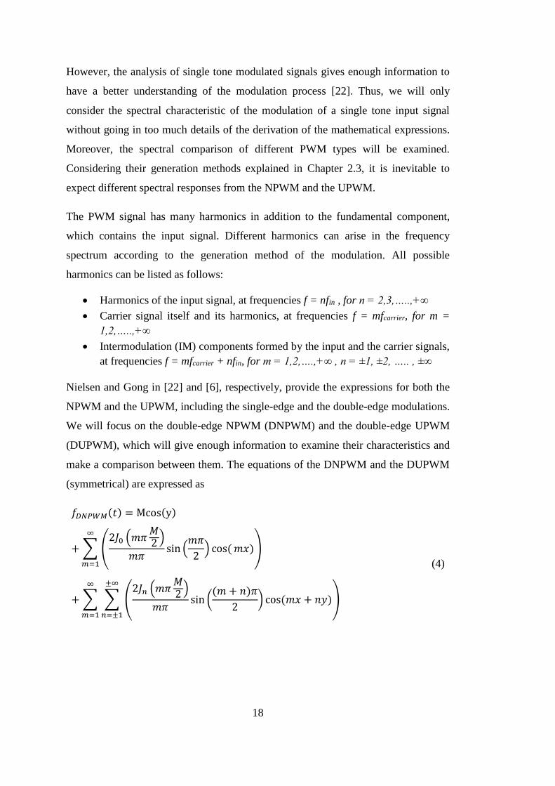
However, the analysis of single tone modulated signals gives enough information to
have a better understanding of the modulation process [22]. Thus, we will only
consider the spectral characteristic of the modulation of a single tone input signal
without going in too much details of the derivation of the mathematical expressions.
Moreover, the spectral comparison of different PWM types will be examined.
Considering their generation methods explained in Chapter 2.3, it is inevitable to
expect different spectral responses from the NPWM and the UPWM.
The PWM signal has many harmonics in addition to the fundamental component,
which contains the input signal. Different harmonics can arise in the frequency
spectrum according to the generation method of the modulation. All possible
harmonics can be listed as follows:
Harmonics of the input signal, at frequencies f = nfin , for n = 2,3,…..,+∞
Carrier signal itself and its harmonics, at frequencies f = mfcarrier, for m =
1,2,…..,+∞
Intermodulation (IM) components formed by the input and the carrier signals,
at frequencies f = mfcarrier + nfin, for m = 1,2,….,+∞ , n = ±1, ±2, ….. , ±∞
Nielsen and Gong in [22] and [6], respectively, provide the expressions for both the
NPWM and the UPWM, including the single-edge and the double-edge modulations.
We will focus on the double-edge NPWM (DNPWM) and the double-edge UPWM
(DUPWM), which will give enough information to examine their characteristics and
make a comparison between them. The equations of the DNPWM and the DUPWM
(symmetrical) are expressed as
𝑓𝐷𝑁𝑃𝑊𝑀(𝑡) = Mcos(y)
+∑ (2𝐽0 (𝑚𝜋
𝑀2)
𝑚𝜋sin (
𝑚𝜋
2) cos(𝑚𝑥))
∞
𝑚=1
+∑ ∑ (2𝐽𝑛 (𝑚𝜋
𝑀2)
𝑚𝜋sin (
(𝑚 + 𝑛)𝜋
2) cos(𝑚𝑥 + 𝑛𝑦))
±∞
𝑛=±1
∞
𝑚=1
(4)

19
𝑓𝐷𝑈𝑃𝑊𝑀 =∑(2𝐽𝑛 (𝑛𝜋
𝑀2 𝑞)
𝑛𝜋𝑞sin ((𝑞 + 1)
𝑛𝜋
2) cos(𝑛𝑦))
∞
𝑛=1
+∑ (2𝐽0(𝑚𝜋
𝑀2 )
𝑚𝜋sin (
𝑚𝜋
2) cos(𝑚𝑥))
∞
𝑚=1
+∑ ∑ (2𝐽𝑛 ((𝑛𝑞 + 𝑚)
𝜋𝑀2 )
(𝑛𝑞 + 𝑚)𝜋sin ((𝑚 + 𝑛(1 + 𝑞))
𝑛𝜋
2) cos(mx + ny)) ,
±∞
𝑛=±1
∞
𝑚=1
(5)
where, M is the “modulation index”, which is the ratio between the peak-to-peak
amplitudes of the input signal and the carrier signal. win and wcarrier are the angular
frequency of the input and carrier signal, respectively. q defines the ratio between win
and wcarrier . Jn is the nth-order Bessel function of the first kind. n and m are the indices
of the harmonics of the input and carrier signal, respectively. The carrier signal is
denoted as x = wcarriert while the input signal as y = wint. The harmonic components
and their amplitudes for DNPWM and DUPWM are tabulated in Table 1 and 2,
respectively.
Table 1 Harmonic Components of the DNPWM
Harmonic Component Amplitude
m’th harmonic of carrier 2𝐽0 (𝑚𝜋
𝑀2)
𝑚𝜋sin (
𝑚𝜋
2)
IM-component of carrier
and input
2𝐽𝑛 (𝑚𝜋𝑀2)
𝑚𝜋sin (
(𝑚 + 𝑛)𝜋
2)
Table 2 Harmonics Components of the DUPWM
Harmonic Component Amplitude
n’th harmonic of input 2𝐽𝑛 (𝑛𝜋
𝑀2 𝑞)
𝑛𝜋𝑞sin ((𝑞 + 1)
𝑛𝜋
2)
m’th harmonic of carrier 2𝐽0(𝑚𝜋
𝑀2 )
𝑚𝜋sin (
𝑚𝜋
2)
IM-component of carrier
and input
2𝐽𝑛 ((𝑛𝑞 +𝑚)𝜋𝑀2 )
(𝑛𝑞 +𝑚)𝜋sin((𝑚 + 𝑛(1 + 𝑞))
𝑛𝜋
2)

20
One of the most critical and major outcome of the comparison between the NPWM
and the UPWM is that there is no direct harmonics of the input signal in the NPWM
contrary to the UPWM [21]. In other words, the UPWM introduces distortions at both
the frequency of the input signal itself and its harmonics. This is very important,
especially for Class D power amplifiers, because the direct harmonics of the input
signal will be involved in the frequency band of interest, which lies between the
frequencies of the input signal and the carrier signal. For the NPWM, being free of
direct harmonics of the input signal has a serious advantage over the UPWM since the
input signal can be re-constructed from the PWM signal by appropriate filtering, while
the reconstruction filter will be impractical in the UPWM due to the direct harmonics
of the input signal [22], [24].
Vasca and Iannelli in [20] have given a detailed analysis for different NPWM methods.
The analyses are performed based on an input signal consisting of a DC component R0
and a single tone sinusoidal component with an amplitude of R1 and a frequency of win
shown as
𝑖𝑛(𝑡) = 𝑅0 + 𝑅1 cos(𝑤𝑖𝑛𝑡). (6)
The NPWM can further be sub-categorized with respect to the voltage rails of the
signals forming the modulation procedure; unipolar-modulation and bipolar-
modulation [20]. The voltage rails for both modulation types are listed in Table 3. The
rest of this part will focus on the analysis of the NPWM for both bipolar and unipolar
versions.
Table 3 Peak values of the signals for unipolar and bipolar modulation
Unipolar Modulation Bipolar Modulation
Input Carrier PWM Input Carrier PWM
Peak 0 to R0+R1 0 to Cm 0 to A - R1 to R1 - Cm/2 to Cm/2 - A/2 to A/2

21
2.4.1. Unipolar Trailing-Edge Naturally-Sampled PWM
For demonstration purpose, the input signal is chosen as a sine wave with R0 = 0.5 V,
R1 = 0.2 V, fin = 100 kHz, and the carrier signal is a saw-tooth wave with fcarrier = 1
MHz, which rails between 0 and 1 V (Cm = 1 V). Similarly, the generated PWM signal
switches from 0 V to 1 V (A = 1 V). The modulation can be seen in Figure 14 and its
mathematical expression is given as
𝑓𝑁𝑃𝑊𝑀(𝑡) =𝑅0𝐶𝑚
+𝑀
2cos(y)
+ ∑1
𝑚𝜋(sin(𝑚𝑥) − 𝐽0(𝑚𝜋𝑀) 𝑠𝑖𝑛 (𝑚𝑥 − 2𝑚𝜋
𝑅0𝐶𝑚
))
+∞
𝑚=1
+ ∑ ∑𝐽𝑛(𝑚𝜋𝑀)
𝑚𝜋sin (
𝑛𝜋
2− 𝑚𝑥 − 𝑛𝑦 + 2𝑚𝜋
𝑅0𝐶𝑚
)
±∞
𝑛=±1
+∞
𝑚=1
.
(7)
Figure 14 The unipolar trailing-edge naturally-sampled pulse width modulation

22
2.4.2. Bipolar Trailing-Edge Naturally-Sampled PWM
For demonstration, the input signal is chosen as a sine wave with R0 = 0 V, R1 = 0.2
V, fin = 100 kHz and the carrier signal is a saw-tooth wave with fcarrier = 1 MHz, which
swings between -0.5 V and 0.5 V (Cm = 1 V). Similarly, the generated PWM signal
rails from -0.5 V to 0.5 V (A = 1 V). The modulation can be seen in Figure 15 and its
mathematical expression is given as
𝑓𝐷𝑁𝑃𝑊𝑀(𝑡) =
𝑀
2cos(y)
+ ∑1
𝑚𝜋(cos(𝑚𝜋) − 𝐽0(𝑚𝜋𝑀)) sin(𝑚𝑥)
+∞
𝑚=1
+ ∑ ∑𝐽𝑛(𝑚𝜋𝑀)
𝑚𝜋sin (
𝑛𝜋
2−𝑚𝑥 − 𝑛𝑦) .
±∞
𝑛=±1
+∞
𝑚=1
(8)
Figure 15 The bipolar trailing-edge naturally-sampled pulse width modulation

23
2.4.3. Unipolar Leading-Edge Naturally-Sampled PWM
For demonstration purposes, the input signal is chosen as a sine wave with R0 = 0.5 V,
R1 = 0.2 V, fin = 100 kHz and the carrier signal is a saw-tooth wave with fcarrier = 1
MHz, which rails between 0 and 1 V (Cm = 1 V). Similarly, the generated PWM signal
switches from 0 V to 1 V (A = 1 V). The modulation can be seen in Figure 16 and its
mathematical expression is given as
𝑓𝑁𝑃𝑊𝑀(𝑡) =
𝑅0𝐶𝑚
+𝑀
2cos(y)
− ∑1
𝑚𝜋(sin(𝑚𝑥) − 𝐽0(𝑚𝜋𝑀) 𝑠𝑖𝑛 (𝑚𝑥 + 2𝑚𝜋
𝑅0𝐶𝑚
))
+∞
𝑚=1
− ∑ ∑𝐽𝑛(𝑚𝜋𝑀)
𝑚𝜋sin (
𝑛𝜋
2−𝑚𝑥 − 𝑛𝑦 − 2𝑚𝜋
𝑅0𝐶𝑚
) .
±∞
𝑛=±1
+∞
𝑚=1
(9)
Figure 16 The unipolar leading-edge naturally-sampled pulse width modulation

24
2.4.4. Bipolar Leading-Edge Naturally-Sampled PWM
For demonstration, the input signal is chosen as a sine wave with R0 = 0 V, R1 = 0.2
V, fin = 100 kHz and the carrier signal is a saw-tooth wave with fcarrier = 1 MHz, which
swings between -0.5 V and 0.5 V (Cm = 1 V). Similarly, the generated PWM signal
rails from -0.5 V to 0.5 V (A = 1 V). The modulation can be seen in Figure 17 and its
mathematical expression is given as
𝑓𝐷𝑁𝑃𝑊𝑀(𝑡) =
𝑀
2cos(y)
− ∑1
𝑚𝜋(cos(𝑚𝜋) − 𝐽0(𝑚𝜋𝑀)) sin(𝑚𝑥)
+∞
𝑚=1
− ∑ ∑𝐽𝑛(𝑚𝜋𝑀)
𝑚𝜋sin (
𝑛𝜋
2−𝑚𝑥 − 𝑛(𝑦 + 𝜋))
±∞
𝑛=±1
+∞
𝑚=1
.
(10)
Figure 17 The bipolar leading-edge naturally-sampled pulse width modulatio

25
2.4.5. Unipolar Double-Edge Naturally-Sampled PWM
For demonstration purposes, the input signal is chosen as a sine wave with R0 = 0.5 V,
R1 = 0.2 V, fin = 100 kHz and the carrier signal is a triangle wave with fcarrier = 1 MHz,
which rails between 0 V and 1 V (Cm = 1 V). Similarly, the generated PWM signal
switches from 0 V to 1 V (A = 1 V). The modulation can be seen in Figure 18 and its
mathematical expression is given as
𝑓𝑁𝑃𝑊𝑀(𝑡) =
𝑅0𝐶𝑚
+𝑀
2cos(y)
+ ∑2
𝑚𝜋𝐽0 (
𝑚𝜋𝑀
2) sin (𝑚𝜋
𝑅0𝐶𝑚
) cos(𝑚𝑥)
+∞
𝑚=1
+ ∑ ∑2
𝑚𝜋𝐽𝑛 (
𝑚𝜋𝑀
2) sin ((2𝑚
𝑅0𝐶𝑚
+ 𝑛)𝜋
2) cos(𝑚𝑥 + 𝑛𝑦).
±∞
𝑛=±1
+∞
𝑚=1
(11)
Figure 18 The unipolar double-edge naturally-sampled pulse width modulation

26
2.4.6. Bipolar Double-Edge Naturally-Sampled PWM
For demonstration, the input signal is chosen as a sine wave with R0 = 0 V, R1 = 0.2 V,
fin = 100 kHz and the carrier signal is a triangle wave with fcarrier = 1 MHz, which
swings between -0.5 V and 0.5 V (Cm = 1 V). Similarly, the generated PWM signal
rails from -0.5 V to 0.5 V (A = 1 V). The modulation can be seen in Figure 19 and its
mathematical expression is given as
𝑓𝑁𝑃𝑊𝑀(𝑡) =
𝑀
2cos(y)
+ ∑2
𝑚𝜋𝐽0 (
𝑚𝜋𝑀
2) sin (
𝑚𝜋
2) cos(𝑚𝑥)
+∞
𝑚=1
+ ∑ ∑2
𝑚𝜋𝐽𝑛 (
𝑚𝜋𝑀
2) sin ((𝑚 + 𝑛)
𝜋
2) cos(𝑚𝑥 + 𝑛𝑦).
±∞
𝑛=±1
+∞
𝑚=1
(12)
Figure 19 The bipolar double-edge naturally-sampled pulse width modulation

27
Considering types of the NPWM, as Vasca and Iannelli stated in [20] that the spectral
response of the trailing-edge and the leading-edge NPWM are the same for both
bipolar and unipolar modulation versions. Figure 20 shows the comparison between
the amplitude spectrum of the bipolar trailing-edge and leading-edge NPWM, which
correspond to cases in Chapter 2.4.2 and 2.4.4, respectively.
Figure 20 The amplitude spectrum comparison of the bipolar trailing-edge and
leading-edge NPWM
Another critical observation is that the double-edge modulation has far fewer
harmonics compared to the single edge modulation (trailing or leading edge),
regardless of whether uniform sampling or natural sampling is used [20]. In other
words, choosing a triangle wave as a carrier results in a modulation with reduced
harmonic distortion compared to a saw-tooth carrier wave [21], [22]. As an example,
the amplitude spectrum of the bipolar single-edge NPWM corresponding to the case
in Chapter 2.4.2 (trailing-edge) or 2.4.4 (leading-edge) is compared with the amplitude
spectrum of the bipolar double-edge NPWM corresponding to the case in Chapter

28
2.4.6. As it is shown in Figure 21, the double-edge modulation performs better
harmonic performance over the single-edge modulation.
Figure 21 The amplitude spectrum comparison between the bipolar single-edge
NPWM and the bipolar double-edge NPWM
2.5 Selection of Pulse Width Modulation Method
The types and spectral analysis of the different PWM types are covered in Chapter 2.3
and Chapter 2.4, which will be a guide to determine the type of PWM employed in the
PWM IC that is presented in this work.
Firstly, it is required to select the sampling type, which will be used in the modulation.
As it is covered in Chapter 2.4, the uniform sampling brings distortion at the frequency
of the input signal itself and its harmonics besides the other harmonics related to the
carrier wave. On the contrary, the natural sampling does not introduce harmonics at
the input signal frequency. Because of this reason, the natural sampling is chosen as
the sampling method of the presented PWM IC.

29
Secondly, the double-edge modulation is selected over the single-edge modulation
since it performs better harmonics performance compared to the single-edge
modulation. This means that a triangle wave will be used as a carrier instead of a saw-
tooth wave.
Another selection should be made in terms of the voltage polarity of the signals
participated in the modulation process. The mathematical expressions for the unipolar
double-edge NPWM and the bipolar double-edge NPWM will lead us to make a
comparison between them. As it can be seen in (12), the IM harmonics of the input
and the carrier signals occurring at the frequency of mfcarrier+nfin are eliminated if m+n
is even due to sin[(m+n)π/2] being equal to zero for the bipolar modulation. In other
words, the IM harmonics related to even-order harmonics (where m and n are even)
and odd-order harmonics (where m and n are odd) are diminished in the case of the
bipolar modulation as it is shown in Figure 21. To obtain the same results from the
unipolar modulation, the term
𝑠𝑖𝑛 ((2𝑚𝑅0𝐶𝑚
+ 𝑛)𝜋
2) , (13)
should be equal to zero when m+n is even. The term (13) can only be equal to zero by
making the term
2𝑚𝑅0𝐶𝑚
+ 𝑛, (14)
be an even number. To be able to satisfy this constraint for m+n is even, the term
2R0/Cm should be an odd number.
The bipolar modulation is not preferred since it requires a negative supply voltage as
well as a positive supply voltage while the unipolar operation uses a single positive
supply voltage. However, the PWM IC should satisfy the term 2R0/Cm be an odd
number in its circuit design.
To sum up, the presented PWM IC uses the unipolar naturally sampled double-edge
modulation type as the pulse width modulation method.


31
CHAPTER III
LITERATURE REVIEW ON PULSE WIDTH
MODULATION IMPLEMENTATION
This chapter covers the literature background on the implementation of pulse width
modulation. The review of the literature is sub-categorized with respect to the
implementation domain as digital and analog, which are provided in Section 3.1 ad
3.2, respectively. Section 3.3 provides the evaluation of different implementation
types.
3.1 Digital Implementation
The PWM can be digitally implemented using an application specific integrated circuit
(ASIC) or generic digital integrated circuits such as a field-programmable gate array
(FPGA) or a digital signal processor (DSP). FPGAs and DSPs are capable of many
digital functions and they are very common in the world-market. Since there are low
cost/high performance FPGAs or DSPs available, they are very popular in digital
implementation of the PWM. Besides, there are many ASICs for PWM in the
literature, where more customized operation is required.
The digital PWM is generally used in the digital control loops of DC-DC switching
power converters [25]. The block diagram of a digitally controlled DC-DC switching
power converter is shown Figure 22. The digital controller consists of an A/D
converter, a compensator and a digital pulse width modulator. Basically, the output
voltage of the DC-DC converter is compared with a reference voltage so that an error
voltage is generated. The error voltage is converted into a digital signal using an A/D
converter. The output of the A/D converter is fed to the compensator generating a

32
control signal for the digital pulse width modulator. The digital pulse width modulator
creates the PWM pulses, which will be fed to DC-DC converter [26].
DC-DC
converter
A/Dcompensatordigital PWM
VinVout
VrefVerror
digital control
Figure 22 The digitally controlled DC-DC converter
The major problem of the digitally controlled DC-DC switching power converters is
the limit-cycling (or limit-cycle oscillation), which is caused by the lack of resolution
[25], [27], [28]. The limit cycling is a quantization error based problem and it is a
critical phenomenon, which should be taken into account, especially for the DC-DC
converters requiring strict output voltages. It is inherently obvious that the quantization
effects occur both in the digital pulse width modulator and in the A/D converter
considering the signal chain in the digital control loop of the DC-DC converter [27].
Theoretically, the control loop should work as follows: when the output voltage gets
below its regulation, the control loop should increase the duty cycle of the PWM so
that the output voltage will be compensated and vise-versa. On the other hand, both
digital pulse width modulator and A/D converter suffer from the quantization error.
Let us consider a DC-DC converter with an A/D converter resolution of nA/D-bits and
a digital pulse width modulator resolution of nPWM-bits. The outputs of the A/D
converter and the digital pulse width modulator will have voltage quantization steps
of ∆𝑉𝐴/𝐷 = 𝑉𝑖𝑛/2𝑛𝐴/𝐷 and ∆𝑉𝑃𝑊𝑀 = 𝑉𝑖𝑛/2
𝑛𝑃𝑊𝑀, respectively. If ΔVPWM is larger than
ΔVA/D, the digital pulse width modulator outputs a voltage level, which does not fall
into the A/D converter reading of the reference voltage (zero-error bin) as it is shown
in Figure 23. In other words, it is not possible to represent the needed duty cycle of the
PWM due to the quantization with low resolution. The digital pulse width modulator
will try to generate an output voltage of Vref but it will alternate outside the zero-error

33
bin. This behavior results in an unstable output voltage with oscillations due to the
limit-cycling. To overcome the limit-cycle oscillation, the bit resolution of the digital
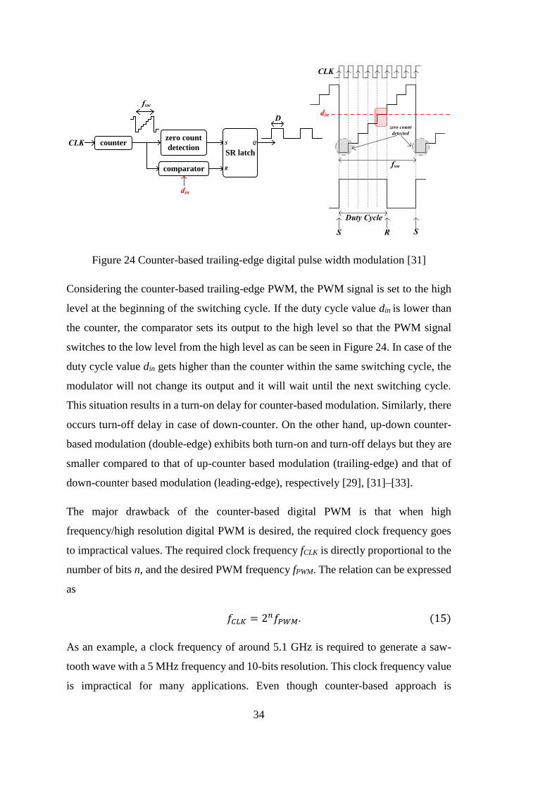
pulse width modulator should be increased [27]–[29]
Figure 23 Limit cycling phenomenon in digitally controlled DC-DC converters [27]
In the literature, there are many works and researches for obtaining digital PWM. The
detailed reviews of their implementations are beyond the scope of this work. However,
the results obtained from different PWM implementations will be discussed by
considering the maximum achievable PWM frequency with highest resolution.
3.1.1 Counter-based Digital Pulse Width Modulation
The most common way of the digital PWM implementation is the counter-based digital
PWM, which can be employed in both general purpose digital ICs and ASICs. This
method can be considered as the digital implementation of conventional PWM [30].
In counter-based method, the carrier signal is generated by using a counter. Thus, the
switching edge of the PWM is determined by the counter type. In case of an up-down
counter, the modulation is specified as the double-edge modulation. The use of an up-
counter depicts the trailing-edge modulation, while the use of a down-counter depicts
the leading-edge modulation [31]. As an example, the trailing-edge digital PWM based
on counter topology is shown in Figure 24.
34
din
Duty Cycle
S R S
fsw
zero count
detected
CLK
counterzero count
detection
comparator
SR latch
D
R
S QCLK
din
fsw
Figure 24 Counter-based trailing-edge digital pulse width modulation [31]
Considering the counter-based trailing-edge PWM, the PWM signal is set to the high
level at the beginning of the switching cycle. If the duty cycle value din is lower than
the counter, the comparator sets its output to the high level so that the PWM signal
switches to the low level from the high level as can be seen in Figure 24. In case of the
duty cycle value din gets higher than the counter within the same switching cycle, the
modulator will not change its output and it will wait until the next switching cycle.
This situation results in a turn-on delay for counter-based modulation. Similarly, there
occurs turn-off delay in case of down-counter. On the other hand, up-down counter-
based modulation (double-edge) exhibits both turn-on and turn-off delays but they are
smaller compared to that of up-counter based modulation (trailing-edge) and that of
down-counter based modulation (leading-edge), respectively [29], [31]–[33].
The major drawback of the counter-based digital PWM is that when high
frequency/high resolution digital PWM is desired, the required clock frequency goes
to impractical values. The required clock frequency fCLK is directly proportional to the
number of bits n, and the desired PWM frequency fPWM. The relation can be expressed
as
𝑓𝐶𝐿𝐾 = 2𝑛𝑓𝑃𝑊𝑀. (15)
As an example, a clock frequency of around 5.1 GHz is required to generate a saw-
tooth wave with a 5 MHz frequency and 10-bits resolution. This clock frequency value
is impractical for many applications. Even though counter-based approach is

35
advantageous in terms of its ease in implementation and linearity, it is not suitable for
high frequency/high resolution digital PWM applications due to the high clock
frequency need [34]. Besides, it exhibits modulation delays.
3.1.2 Delay-line based Digital Pulse Width Modulation
One other method is the delay-line based digital PWM as can be seen in Figure 25. It
consists of 2n delay cells and 2n x 1 multiplexer for an n-bit digital PWM. The delay of
each cell determines the time step and the total time delay selected by the multiplexer
generates the PWM signal. The selection of the multiplexer is controlled by the n-bit
duty cycle signal d[n]. The PWM signal is set to the high level by the clock signal and
it is reset when the multiplexer makes its selection.
d[n]
Figure 25 The delay-line based digital pulse width modulation
Delay-line based approach uses the clock frequency as the PWM frequency so that it
eliminates the high clock frequency requirement of the counter-based modulation and
also minimize the power consumption. The one of the major drawback is the large chip
area consumption when high resolution is desired. The case of higher resolution
requires more delay cells and larger multiplexer, which results in a larger chip area. In
the design, the total delay resulted from the delay cells should be designed in such a
way that the maximum delay obtained should be equal to the clock frequency for
proper operation. However, the delay of a cell is a function of supply voltage and is
vulnerable to process and temperature variations. This can create a degradation in the
performance of the operation. Another critical issue is the matching of the high number

36
of delay cells, where high resolution is required. Device mismatch can create a
linearity problem [34]–[37].
The work in [31] presents a digital pulse width modulator integrated circuit, which
employs delay-line based architecture. The measurement results reveal that the chip
operates at a maximum PWM frequency of 1 MHz with 6-bits resolution. Another
delay-line based digital PWM IC is presented in [38]. For this IC, the simulation results
offer a digital PWM with a frequency of 1 MHz with 11-bits resolution.
3.1.3 Hybrid Digital Pulse Width Modulation
Hybrid digital PWM is combination of delay-line based and counter-based methods as
can be seen in Figure 26. The resolution of the hybrid modulation is arranged in such
a way that n-bit PWM resolution is obtained using an nc-bit counter and nd-bit delay
line, where n=nc+nd. In PWM generation, the most significant bit (MSB) of the duty
cycle is determined by the counter-based part and the least significant bit (LSB) is
controlled by the delay-line based part. Moreover, the reverse operation can be applied
to determine LSB and MSB of the duty cycle [5], [39].
Figure 26 Hybrid digital pulse width modulation
Hybrid digital PWM offers higher resolution/high frequency PWM with lower clock
frequency as opposed to the counter-based modulation and consumes smaller chip area
as opposed to the delay-line based modulation. However, it still falls short in terms of
obtaining high frequency/high resolution PWM signal due to its discrete nature, which
requires very sharp filters to reduce harmonics and switching glitches [5], [39], [40].

37
The simulation work in [41] proposes a digital PWM operation with 2 MHz frequency
and 4-bits resolution requiring 32 MHz clock frequency. Another simulation work in
[42] offers a PWM generation with a frequency of 500 kHz with 11-bits resolution
operating at 16 MHz clock frequency. The measurement results of the digital PWM
controller IC presented in [39] reveals a digital PWM with 8-bits and 1 MHz frequency
running with a clock frequency of 8 MHz. The work in [34] is a FPGA implementation
of the hybrid digital PWM and experimental results show a PWM signal with 10-bits
resolution and 780 kHz frequency.
Table 4 summarizes the results obtained from several works based on the digital
implementations of the PWM.
Table 4 Summary of several works based on the digital PWM implementation
[43] [38] [41] [42] [39] [34]
Method delay-line delay-line Hybrid Hybrid Hybrid Hybrid
PWM
frequency
1 MHz 1 MHz 2 MHz 500 kHz 1 MHz 780 kHz
Resolution 6 bits 11-bits 4 bits 11bits 8 bits 10 bits
Clock
frequency
1 MHz 1 MHz 32 MHz 16 MHz 8 MHz 25 MHz
3.2 Analog Implementation
The implementation of the PWM in analog domain can occur by using an integrated
circuit or discrete circuit specified for PWM. The major advantage of the analog
implementation compared to the digital one is improved resolution, theoretically
infinite, while one of its major design challenge is to generate the carrier signal (either
saw-tooth or triangle wave) with good linearity and high frequency [44].
Implementing PWM on discrete level requires many active and passive components.
The use of many circuit components results in reduced accuracy due to their tolerances
and serious area consumption compared to IC level design. One way of discrete level
analog implementation of PWM is based on the circuit realization of the naturally-
sampled double-edge PWM. The circuit in [8] is an example of this implementation

38
and its schematic is shown in Figure 27. It basically involves an error amplifier, a
triangle wave generator, and a comparator. The critical issue is to determine the
frequency of the triangle wave, which gives the frequency of the PWM. In [8], the
frequency of the triangle wave ftri is calculated as
𝑓𝑡𝑟𝑖 =𝑅6
4𝑅7𝑅5𝐶3. (16)
The tolerance of capacitor C3 and resistors R5, R6 and R7 are directly responsible for
the frequency error of the triangle wave and PWM. The measurement results of the
circuit in [8] shows that the circuit generated a triangle wave with a frequency of 477
kHz, where the frequency value is set to 500 kHz in the design. Thus, the circuit
dramatically suffers from the frequency error.
Error amplifier
Triangle Wave
Generator
Comparator
Figure 27 Discrete level analog PWM implementation example [8]
Another approach for analog implementation is the phase-locked loop (PLL) based
PWM generation. This type of PWM is widely used in power-line and wireless
applications, where the PWM is used to drive the power stage of a class-D power

39
amplifier [7]. The work in [44] is an integrated class-D PA with PLL-based PWM
driver and it is presented in Figure 28.
loop
filterVCO
clock
generator
phase
detector
power
stageVin Vout
Figure 28 A Class D power amplifier with PLL-based PWM driver [44]
In PLL-based PWM generation, the phase of a VCO (voltage-controlled oscillator) is
obtained by converting the difference between the output signal and the input signal.
Then, a phase detector generates the PWM signal as an output by comparing the phase
of VCO with that of a reference clock. The major advantage of the PLL-based PWM
generation over the triangle or saw-tooth based PWM generation is the replacement of
a high-linearity carrier signal with a reference clock, which does not have any
requirement on its linearity. This situation gives a way to high frequency PWM
operation [7]. On the other hand, the major problem of the PLL-based PWM
generation is its harmonic characteristics due to the non-linearity of VCO. As we have
discussed in Chapter 2.4, there are many harmonic components in the frequency
spectrum of the PWM, which is generated by an input signal with the frequency of fin
and a carrier signal with the frequency of fc. The non-linearity of VCO results in further
intermodulation harmonics of the spurs related to input and carrier signals. As an
example, there are spurs at fc+nfin and fc+(n+2)fin in the spectrum of the PWM by its
nature. However, the second harmonic distortion of VCO results in down-converting
of these spurs into the baseband and appearing as a distortion at 2fin. Similarly, the
third harmonic distortion of VCO can cause that spurs at fc+2nfin and 2fc+nfin generate
third-order intermodulation distortion [44]. In other words, PLL-based approach
introduces extra harmonics caused by the non-linear behavior of the VCO in addition
to the harmonics related to the input and the carrier signals. These unwanted spurs will
be located at baseband. Thus, in order to reduce the harmonic distortion at the
baseband, PLL-based PWM ICs are forced to work at higher frequencies, around 100
MHz range even if the input signal frequency is around 10 kHz range. However, the
switching loss of a power MOSFET is directly proportional to the switching frequency

40
(PWM frequency). As the PWM frequency rises to several 10 MHz range, the
switching losses of the power MOSFETs increase reducing the efficiency of the system
to impractical values.
The work in [45] is an analog implementation of the double-edge uniformly-sampled
PWM in IC level. The block diagram of the circuit is shown in Figure 29. The circuit
involves a sample/hold circuit to perform uniform sampling, a triangle wave generator
and a comparator.
Comparator
-
+
Sample/Hold
Circuit
Triangle Wave
Generator
Figure 29 Analog uniform sampling PWM implementation [45]
For triangle wave generation, the idea of taking integral of a square wave is used,
which is implemented with an OPAMP circuit as it is shown in Figure 30. Moreover,
the integration is based on charging and discharging of a capacitor with a time constant
of RC.
OPAMP
-
+
C
RVin
Vout
Figure 30 Ideal OPAMP integrator circuit
The major problem of the integration-based triangle wave generation is the linearity.
Also, the slew rate of the OPAMP will limit the operation for high frequency PWM
operation.

41
3.3 Evaluation
The works in the literature about PWM implementation have been covered based on
the implementation domain as analog and digital. The design challenge of the digital
implementation of PWM is to satisfy high resolution/high frequency PWM operation.
However, the digital PWM always suffers from the lack of resolution since it is
inherently a discrete solution. Moreover, limited resolution results in reduced accuracy
and there occurs additional delays related to sampling and processing times [31], [46].
Considering the analog domain, the discrete level solutions require many active and
passive components, which dramatically affect the PWM operation due to their
tolerances. Moreover, they consume too much circuit area. PLL-based PWM
generation has many unwanted harmonics in their baseband due to the VCO in its
circuit topology and they are not preferred especially for audio and SONAR
applications. Integration-based PWM implementation is insufficient in terms of
generating the linear triangle wave otherwise higher harmonic distortion is obtained.
The next chapter is dedicated to the design, analysis and implementation of the
presented high frequency pulse width modulation integrated circuit. The presented
PWM IC offers an architecture, that generates the triangle wave with constant current
charging/discharging based method so that triangle wave can be obtained with high
linearity. It performs naturally-sampled PWM in analog manner eliminating the
resolution problem as will be detailed in the following section.


43
CHAPTER IV
IMPLEMENTATION
In this section, the implementation of the PWM IC is presented. In Chapter 4.1, the
design specifications of the PWM IC are determined. Chapter 4.2 covers the design
and the circuit analysis of the PWM IC. Its circuit architecture is provided starting with
the major blocks down to the sub-blocks. The simulation results of the key sub-blocks
are summarized. Chapter 4.3 provides the full-chip layout and the methods that have
been followed in the physical design of the PWM IC. In Chapter 4.4, the top-level
simulation of the PWM IC is given.
4.1 Design Specifications of the PWM IC
As expressed in Chapter 2.5, the presented PWM IC employs the unipolar double-edge
naturally-sampled pulse width modulation. The selection of the modulation type
determines some of the specification by itself. The unipolar modulation type requires
a single supply operation whereas, the double-edge modulation type requires the
generation of a triangular wave as the carrier. The natural sampling indicates that the
modulation is required to occur at the same time instant with the sampling of the input
signal by the carrier signal. Extra features are considered to make the PWM IC be a
candidate for many applications, as will be listed later in this section. The fundamental
specifications and features determined for the PWM IC are listed as follows:
4.1.1 High Frequency PWM Operation
The maximum operating frequency of the PWM IC is specified as 5 MHz considering
the trend of high frequency operation in the SMPSs and the class D PAs. Another
driving point is the SONAR applications, where the high frequency operation (up to 1
MHz) is required [17]. It is obvious that the requirement of generating a PWM signal

44
up to 5 MHz frequency inherently implies the generation of a triangle wave with 5
MHz frequency. This should also be accomplished by the PWM IC.
4.1.2 Two Output Generation
In the SMPSs and the class D PAs, the PWM signal is fed to a gate driver chip, which
drives the switching MOSFETs. Gate drivers being capable of operating at several
MHz are available in the market. These products are designed in such a way that they
need both a PWM signal and its complement as the inputs to operate [47], [48].
Considering this situation, the PWM IC is required to generate a PWM signal and its
complement up to 5 MHz frequency as the outputs.
4.1.3 Adjustable PWM Frequency
The PWM IC is required to generate the PWM signal with adjustable frequency up to
5 MHz. This feature gives an opportunity to the PWM IC for being applicable in
various areas having different PWM frequency requirement.
4.1.4 Synchronized Operation
The PWM IC in design should have external synchronization capability. This is
required in building phased-array SONAR systems. As it is covered in Chapter 2.2.3,
the PWM is used as the driving method in the class D PAs. Many phased-array active
SONAR systems use class D PAs in their transmitters. Very similar to the phased-
array systems used in the wireless communication and RADAR systems, the acoustic
waves generated by the phased array can be electronically steered without moving the
transducers. By this way, the beams are targeted to different directions by adjusting
the relative phases of transducer elements, without the need of a mechanical
movement. In such applications, the accurate controlling of the phases is very
important. For example, when the inputs of the PAs are in phase, the time delay
between outputs of the PAs should theoretically be zero. If there is a time delay
between the outputs of the PAs, there will be a phase shift between them even if no
intentional phase shift is given. This situation will degrade the accuracy of the
controlling of the phased array. In order to have phase matched outputs from multiples
of class D PAs in a phased-array system, the PWM signal driving them should also be
in phase. Although it is obvious that there will be some phase-error contribution due

45
to the fabrication tolerances, generation of PWM signals with the best possible phase
matching is important.
Considering two AC sinusoidal signals as in Figure 31, the expression for the phase
shift ∆ɸ between them is calculated as
∆ɸ = 360° × 𝑓 × ∆𝑡 , (17)
where f is the frequency of the signals, and ∆t is the time delay between signals.
∆t
Figure 31 Two AC signal with a time delay of ∆t
There is no magic number for the maximum tolerable phase error, since it is a system-
dependent parameter, which will change with respect to a number of elements, such as
the order of the phased array system. For this application, it was decided to have a
maximum of 10 of a phase shift error at a frequency of 500 kHz. In other words, when
in-phase AC input signals are applied to several PWM ICs, the coded PWM outputs
should have a maximum time-delay skew of at most 5.5 ns.

46
4.2 Design and Analysis of the PWM IC
By definition, a PWM signal is generated by comparing an input signal with a high
frequency carrier signal. The proposed PWM IC follows this basic idea. The block
diagram of the presented PWM IC is shown in Figure 32. The PWM IC consists of
two main blocks; the comparator, and the triangle wave generator. The triangle wave
generator has three sub-blocks; current-reference circuit, the constant source/sink
currents generator circuit, and the charge/discharge control circuit. The PWM IC
requires an external clock signal and the input coding signal to output the coded PWM
signal and its complement. It also requires one off-chip resistor and one off-chip
capacitor to operate. The reason for the usage of these two external components will
later be discussed.
Charge/Discharge
Control Circuit
Current
Reference
Constant
Source/Sink
Currents
Generator
PWM
INPUT
Comparator
PWM IC
C
-
+
CLOCK
R
Triangle Wave Generator
PWM
Figure 32 The block diagram of the presented PWM IC
4.2.1 Triangle Wave Generator
The triangle wave generator is required to generate a high frequency analog triangle
wave with adjustable frequency so that a PWM signal can be obtained with adjustable
frequency. For this purpose, the PWM IC employs a method based on the periodic
charging/discharging of a capacitor with a constant current. In this method, an external
clock signal at the desired operation frequency is used to control the steering
mechanism of the constant sink/source currents. This approach can be understood
better in the light of the basic equation of the current-voltage relation of a capacitor
which is shown as

47
𝐼 = 𝐶Δ𝑉
Δ𝑡∙ (18)
The parameters participated in (18) have individual meanings for the developed
methodology. In (18), I refers to the constant sink/source current, which will
discharge/charge an off-chip capacitor with a capacitance of C. ∆V is the peak-to-peak
amplitude of the triangle wave, which is denoted as Cm in Chapter 2.4. ∆t corresponds
to the half of the PWM (or triangle wave) period which is adjusted by the external
clock signal. Equation (18) is obtained as
𝐶𝑓𝑃𝑊𝑀 =𝐼
2𝛥𝑉 , (19)
if it is written in terms of the frequency of the PWM signal which is denoted as fPWM.
To generate the triangle wave with user-adjustable frequency, it is required to obtain a
relation between the parameters in (19). In case of the values of I and ∆V are held
constant, the multiplication of C and fPWM is equal to a fixed value. Thus, a simple
relation between the external clock frequency and the off-chip capacitance provide the
method of generating a triangle wave (or PWM) with adjustable frequency. The values
of I and ∆V are chosen to be 1 mA and 1 V, respectively. Thus, the multiplication of
C and fPWM is set to 0.0005 meaning that if the frequency of the PWM is selected as 5
MHz, the off-chip capacitor should have a capacitance of 100 pF. Some examples of
this developed method are tabulated in Table 5. It is obvious that this method requires
the employment of an external capacitor. In order to have accurate triangle wave
generation, capacitors with low tolerances are used.
Table 5 The method for adjustment of the PWM (or triangle wave) frequency
Desired PWM(or triangle
wave) Frequency
Required External
Clock Frequency
Required Off-chip
Capacitance
5 MHz 5 MHz 100 pF
1 MHz 1 MHz 500 pF
100 kHz 100 kHz 5 nF
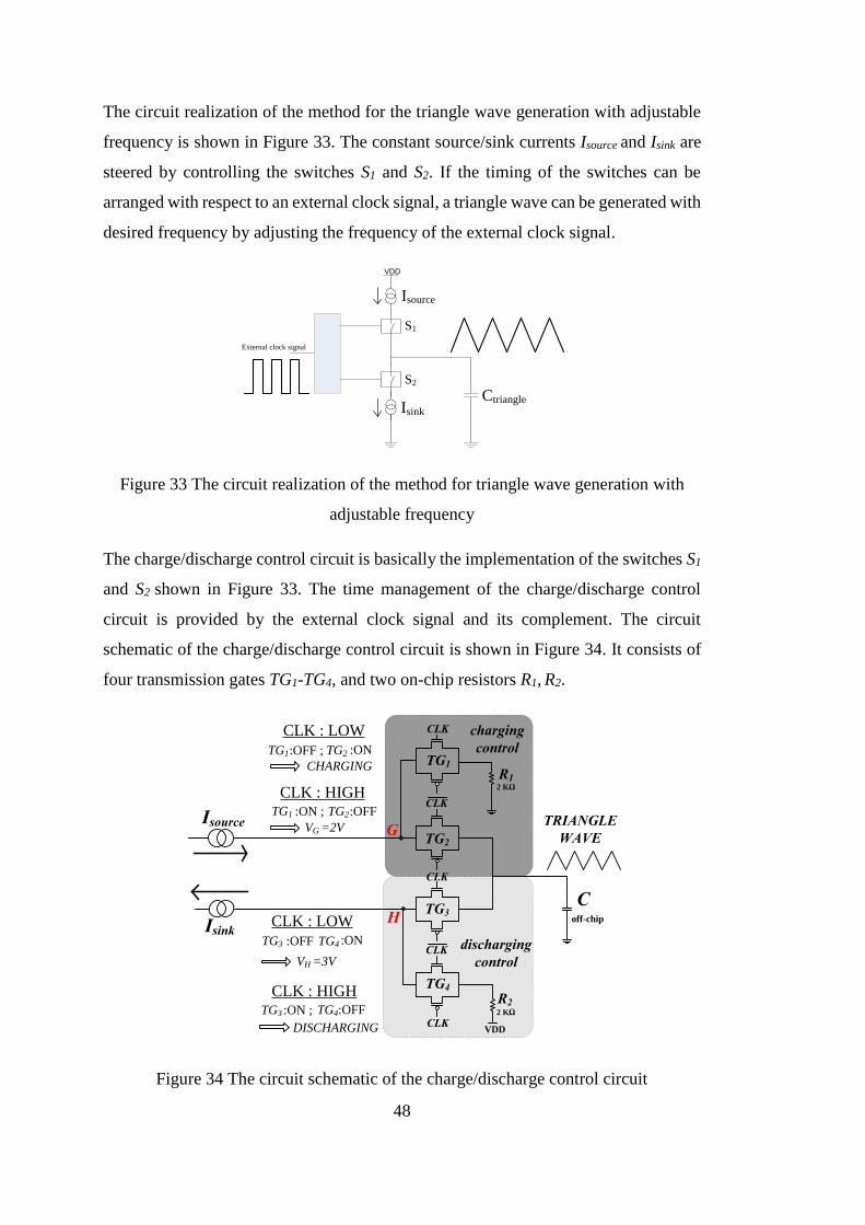
48
The circuit realization of the method for the triangle wave generation with adjustable
frequency is shown in Figure 33. The constant source/sink currents Isource and Isink are
steered by controlling the switches S1 and S2. If the timing of the switches can be
arranged with respect to an external clock signal, a triangle wave can be generated with
desired frequency by adjusting the frequency of the external clock signal.
Isource
S1
Isink
VDD
Ctriangle
S2
External clock signal
Figure 33 The circuit realization of the method for triangle wave generation with
adjustable frequency
The charge/discharge control circuit is basically the implementation of the switches S1
and S2 shown in Figure 33. The time management of the charge/discharge control
circuit is provided by the external clock signal and its complement. The circuit
schematic of the charge/discharge control circuit is shown in Figure 34. It consists of
four transmission gates TG1-TG4, and two on-chip resistors R1, R2.
off-chip
C
2 KΩ
VDD
CLK
2 KΩ
TRIANGLE
WAVEG
H
R1
R2
CLK
CLK
CLK
CLK
TG1
TG2
TG3
TG4
charging
control
discharging
control
Isink
Isource
:OFF TG4 :ON ;TG3
CLK : HIGH
VH =3V
:ON ;TG1 :OFFTG2
CLK : HIGH
VG =2V
DISCHARGING
:OFF
CLK : LOW
TG3 :ONTG4
:ON
CLK : LOW
TG2 :OFF ;TG1
CHARGING
Figure 34 The circuit schematic of the charge/discharge control circuit

49
The clock-controlled charging/discharging mechanism works as follows: when the
external clock is low, TG2 will be “ON” resulting in charging of the off-chip capacitor,
and TG3 will be “OFF” disabling the discharge. When the external clock is high, TG2
will be “OFF” preventing the charging, and TG3 will be “ON” enabling the discharging
path of the off-chip capacitor. Besides, his control circuit ensures the peak-to-peak
value of the triangle wave to be equal to 1 V as follows: When the external clock is
low, TG4 will be “ON” and it will allow the sink current to flow through R2, which will
set the voltage of node H to 3 V. This determines the top-peak value of the triangle
wave. Similarly, when the external clock is high, TG1 will be “ON”, and the source
current will flow through R1 setting the voltage of node G to 2 V. By doing this, a
triangle wave with a peak-to-peak amplitude of 1 V is obtained, which is required with
respect to the method developed for triangle wave generation with adjustable
frequency.
The charge/discharge control circuit will bring another important result. It generates
the triangle wave with a peak-to-peak amplitude of 1 V, and a DC offset of 2.5 V. In
case of an input signal composed of AC and DC components as in (6), its DC value R0
should be set to 2.5 V for full-range operation. Thus, the value of R0 and Cm shown in
(13) are set to 2.5 and 1, respectively, making the term 2D (=R0/Cm) be equal to 5,
which is an odd number. Since 2D is an odd number, the term sin[(2Dm+n)π/2] will
be equal to zero when m and n are both even or odd numbers. As discussed in Chapter
2.4, the PWM IC should satisfy to achieve lower harmonic distortion as in bipolar
modulation.
It is critical to design the transistors employed in the transmission gates by considering
their switching performance. In case of a MOSFET used as a switch, it will be in the
triode (linear) region when the switch is “ON”, and it will be in the cut-off region when
the switch is “OFF”. In the triode region, a MOSFET behaves like a resistor, which is
called as on-resistance [49]. It can be expressed as
𝑅𝑜𝑛 =1
𝜇𝑛𝐶𝑜𝑥(𝑊/𝐿)(𝑉𝐺𝑆−𝑉𝑡ℎ) , (19)
where µn is the mobility of electrons, Cox is the gate oxide capacitance, W is the width
of a MOSFET, L is the effective length of a MOSFET, VGS is the gate-to-source voltage

50
of a MOSFET, and Vth is the threshold voltage of a MOSFET. Besides, W/L is called
as the aspect ratio of a MOSFET.
When current passes through a MOSFET in the triode region, a voltage drop across its
drain-source terminals occurs, which is equal to the multiplication of the on-resistance
and the drain current. This voltage drop can be reduced by lowering the on-resistance
value, which can be achieved by increasing the W/L ratio.
The switching performance of a MOSFET is related to its input capacitance. Larger
input capacitance limits the switching performance of a MOSFET, and the input
capacitance is proportional to W/L ratio. Thus, there is a trade-off between the on-
resistance and the switching performance of a MOSFET. The circuit design and
optimisation is performed considering this trade-off.
Another sub-block of the triangle wave generator is the constant source/sink currents
generator. This circuit is required to generate 1 mA of constant source/sink currents,
which will charge/discharge the off-chip capacitor. The circuit uses the basic idea of
mirroring a current reference to generate the constant source/sink currents. For copying
the current reference, a basic current mirror circuit is designed as is shown in Figure
35.
VDD
M1M2 M3
M4 M5
IrefIref
Isource
Isink
Figure 35 Current mirror circuit for generation of the source and sink currents

51
The source current is generated by the current mirror established by the transistors M2,
M3, and the sink current is mirrored from the reference current with the help of the
transistors M4, M5. Ignoring the channel length modulation, the ratio between the
source/sink currents and the reference current are expressed as
𝐼𝑠𝑖𝑛𝑘
𝐼𝑟𝑒𝑓𝑒𝑟𝑒𝑛𝑐𝑒=
(𝑊/𝐿)5
(𝑊/𝐿)4 (20)
𝐼𝑠𝑜𝑢𝑟𝑐𝑒
𝐼𝑟𝑒𝑓𝑒𝑟𝑒𝑛𝑐𝑒=
(𝑊/𝐿)3
(𝑊/𝐿)2∙ (21)
It is obvious that this circuitry will suffer from the channel length modulation in
practice. This effect will cause an error in the mirroring process [49]. Considering the
current mirror formed by M4 and M5, the ratio between the sink current and reference
current can be written as
𝐼𝑠𝑖𝑛𝑘
𝐼𝑠𝑜𝑢𝑟𝑐𝑒=
(𝑊/𝐿)5
(𝑊/𝐿)4
1+𝜆𝑉𝐷𝑆5
1+𝜆𝑉𝐷𝑆4 , (22)
where λ is the channel length modulation parameter, VDS4 and VDS5 are the drain-to-
source voltages of M4 and M5, respectively. To minimize the copying error between
the reference current and the sink/source currents, it is obvious that the drain-to-source
(or source-to-drain) voltages of the transistors participated in the current mirrors
should be equal. By this way, the effect of the channel length modulation can be
eliminated. For this purpose, the current mirror circuit in Figure 35 is improved to the
circuit as shown in Figure 36. The improvement is achieved by three feedback circuits;
two of them are for the upper current mirrors, and the other one is for the lower current
mirror. The main idea is the equalization the source-to-drain voltages of M2, M3, and
the drain-to-source voltage of M4, M5 with the help of the feedback circuits. The
feedback circuit for the upper current mirrors includes an OPAMP and a PMOS
transistor, while the lower feedback circuit consists of an OPAMP and an NMOS
transistor. The feedback circuits create a negative feedback, and the OPAMP will force
the non-inverting input voltage to be equal to the inverting input voltage. Thus, the
voltages of nodes B, C, and D will be equal, and similarly the voltages of node E and
F. By the help of this feedback mechanism, the channel length modulation effect is
minimized and the copying error in the current mirrors is reduced.

52
VDD
B C D
E
M1M2 M3
M4 M5
F
Iref
Iref
Isource
Isink
B C D
E
M1M2
M6
M4
OP1 OP2
OP3
F
M7
M6
M3
Iref
M5
+
- +
-
VDD
+ -
Isource
Isink
Iref
Figure 36 The improved constant sink/source currents generator circuit
The design of the OPAMP used in all of these the feedbacks requires some points
needed to be considered. An OPAMP in a negative feedback configuration forces the
non-inverting input voltage to be equal to the inverting input voltage. The equalization
of the inputs is exactly satisfied when an OPAMP has infinite open-loop gain. In
reality, an OPAMP has a finite gain, which results in a voltage error between two
inputs. [42], [44], [46]. To minimize the error between the inverting and the non-
inverting inputs, the open-loop gain should be as high as possible. Besides, the stability
of the OPAMP is another parameter that should also be considered for a proper
operation.
For the OPAMP used in the feedback circuit, a two-stage OPAMP topology with
Miller compensation is chosen since high gain with improved stability can be provided
[42], [47]. The circuit schematic of the OPAMP used in the feedback circuit is shown
in Figure 37.
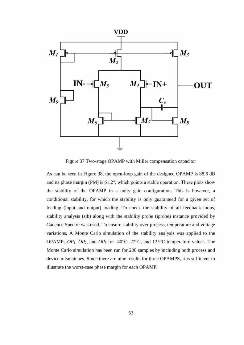
53
IN+IN-
VDD
M1
M2
M3
M4M5
M6 M7 M8
M9
OUT
Cc
Figure 37 Two-stage OPAMP with Miller compensation capacitor
As can be seen in Figure 38, the open-loop gain of the designed OPAMP is 88.6 dB
and its phase margin (PM) is 61.2°, which points a stable operation. These plots show
the stability of the OPAMP in a unity gain configuration. This is however, a
conditional stability, for which the stability is only guaranteed for a given set of
loading (input and output) loading. To check the stability of all feedback loops,
stability analysis (stb) along with the stability probe (iprobe) instance provided by
Cadence Spectre was used. To ensure stability over process, temperature and voltage
variations, A Monte Carlo simulation of the stability analysis was applied to the
OPAMPs OP1, OP2, and OP3 for -40°C, 27°C, and 125°C temperature values. The
Monte Carlo simulation has been run for 200 samples by including both process and
device mismatches. Since there are nine results for three OPAMPS, it is sufficient to
illustrate the worst-case phase margin for each OPAMP.
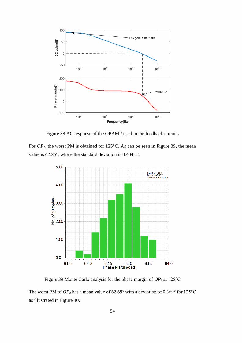
54
Figure 38 AC response of the OPAMP used in the feedback circuits
For OP1, the worst PM is obtained for 125°C. As can be seen in Figure 39, the mean
value is 62.85°, where the standard deviation is 0.404°C.
Figure 39 Monte Carlo analysis for the phase margin of OP1 at 125°C
The worst PM of OP2 has a mean value of 62.69° with a deviation of 0.369° for 125°C
as illustrated in Figure 40.

55
Figure 40 Monte Carlo analysis for the phase margin of OP2 at 125°C
The worst phase margin with 57.12° mean and 0.370° deviation is obtained for OP3,
where the temperature is 125°C, and the result can be seen in Figure 41.
Figure 41 Monte Carlo analysis for the phase margin of OP3 at 125°C

56
As the results shown in Figures 39, 40, and 41 suggest, the OPAMPs employed in
three feedback circuits satisfy a stable operation.
Another sub-block of the triangle wave generator is the current reference circuit, which
is required to generate 100 µA of reference current. For successful triangle wave
generation, it is mandatory to generate the constant source/sink currents robust against
process, voltage, and temperature (PVT) variations, which makes the use of a reference
current be necessary. The current reference circuit should be designed in such a way
that it can be integrated to the rest of the triangle wave generator circuit as it is shown
in Figure 42.
-
+
-
+
-
+
off-chip
C
B C D
E
M1M2
M7
M3
M8
M4 M5
M6
OP1 OP2
OP3
2 KΩ
VDD
CLK
2 KΩ
F
Iref
TRIANGLE
WAVEG
H
R1
R2
CLK
CLK
CLK
CLK
TG1
TG2
TG3
TG4
Iref
VDD
Isource
Isink
Figure 42 The triangle wave generator circuit without current reference
For the current reference, the circuit topology shown in Figure 43 is used. This is
basically a circuit that converts a voltage to a current. This topology is adaptable for
the rest of the triangle wave generator since it sources a current that can be integrated
into the upper current mirror. The resistor shown in the schematic is an external high
accuracy resistor. The system uses an external resistor to generate a very accurate
reference current. It is quite easy to create stable reference voltages in integrated circuit

57
implementations using bandgap references as will be detailed later in this section.
However, since the generation of current depends on resistors, which have very large
variations in integrated circuit implementations (typically +/- 10%), it is impossible to
get stable current generation without trimming. On the other hand, with the usage the
circuit defined in Figure 43, stable current generation can be achieved, thanks to the
availability of accurate external thin-film resistors. The Iref value for this
implementation was chosen as 100 µA. The value of the resistor R can easily be
calculated since the top node of the resistor is forced to the value of the Vref voltage by
the feedback.
To be able to generate a reference current using this circuit, a band-gap reference
circuit is required to provide the Vref voltage. In operation, an OPAMP forces its non-
inverting input voltage to be equal to the inverting input voltage so that the reference
current can be generated through a resistor and a PMOS transistor.
R
Iref
VDD
Vref -
+
Figure 43 The current reference circuit
With the integration of the current reference, the schematic of the triangle wave
generator is shown in Figure 44.

58
VDD
-
+
-
+
-
+
off-chip
C
A
B C D
E
M1 M2
M7
M3
M8
M4 M5
M6
OP4
OP1 OP2
OP3
2 KΩ
VDD
CLK
2 KΩ
R
F
Isource
Isink
Iref
Iref
TRIANGLE WAVEG
H
R1
R2
CLK
CLK
CLK
CLK
TG1
TG2
TG3
TG4
-+
Vref
Figure 44 The triangle wave generator with the current reference
The value of the Vref voltage should be calculated back from the circuit schematic
above, while ensuring all transistors in taking part in the mirroring safely stays in the
saturation regime all the time. In operation, the voltage of node G is set to 3 V during
the charging of the off-chip capacitor by the control circuit. Considering the upper part
of the circuit in Figure 44, the voltages of the nodes B, C, and D will be equal to the
output of the band-gap reference. The output voltage of the band-gap reference should
be arranged in such a way that enough saturation voltage headroom is provided for the
transistor M8 as shown in Figure 44. For this purpose, the output of the band-gap
reference is set to 3.5 V, which means that the value of the resistor is automatically
determined as 35 KΩ to satisfy the reference current of 100 µA.
Figure 45 shows the basic principle of a band-gap reference [50]. The idea behind this
principle is to compensate the negative temperature dependence of the base-to-emitter
voltage of a bipolar transistor with the positive temperature dependence of the thermal
voltage [49], [51].

59
Figure 45 The basic principle of a band-gap reference [50]
The fundamental circuit topology for the voltage-mode current reference is shown in
Figure 46.
Vref
(A) n(A)Q1 Q2
R1
-
+
R2
R3
Figure 46 The conventional voltage-mode band-gap reference circuit [49]
For this circuit, the output expression is given as
𝑉𝑟𝑒𝑓 = 𝑉𝐵𝐸2 + (𝑉𝑇 ln 𝑛) (1 +𝑅2
𝑅3) ∙ (23)
In (23), the positive temperature coefficient (TC) comes from the thermal voltage VT
while the base-to-emitter voltage VBE has a negative TC. Thus, zero TC can be obtained
by arranging the term (1+R2/R3)ln(n) [49]

60
Since a voltage-mode band-gap reference is unable to provide a output voltage larger
than 1.2 V, it is crucial to employ a current-mode band-gap circuit, which can be
designed to satisfy the output voltage of 3.5 V [51]. The current-mode band-gap
reference circuit implemented in the PWM IC can be seen in Figure 47 [52].
START-UP CIRCUIT BAND-GAP CORE
- +Vref
(A) n(A)
X Y
M1
M2
M3
M4 M5
M6M7 M8
VDD
R2 Q1 Q2
R1
R3 R4
Figure 47 The implemented current-mode band-gap reference
The circuit shown in Figure 47 consists of two parts; the band-gap core, and the start-
up circuit. The start-up circuit prevents setting the voltage of node X to zero when the
supply voltage is given and the operation is initialized for the first time. After the
initialization, the band-gap core will be activated and generate the desired output
voltage.
The start-up circuit is designed in such a way that it will be active when the voltage of
node X is zero, and it will be disabled from the band-gap core when the voltage of node
X is greater than the turn-on voltage of the transistor Q1. The start-up circuit has four
diode-connected transistors M1-M4 so that a fixed voltage will be created in the gate of
M5 through M1-M4. This voltage is set to a specific value, which will be enough to
make M5 start conducting current in case of the voltage of node X being zero. Thus,
the band-core will be forced to start-up even if the voltage of node X is zero.

61
The operation of the band-gap core is based on the cancellation of the negative
temperature dependence of the base-to-emitter voltage of a bipolar transistor with the
positive temperature dependence of the thermal voltage [52]. The expression of the
reference voltage Vref is given as
𝑉𝑟𝑒𝑓 = 𝑅4 (𝑉𝐵𝐸1−𝑉𝐵𝐸2
𝑅1+
𝑉𝐵𝐸1
𝑅2) , 𝑅2 = 𝑅3 , (24)
where VBE1 and VBE2 are the base-to-emitter voltages of Q1 and Q2 vertical npn bipolar
transistors, respectively, and R1-R4 are the on-chip resistors.
As in the feedback circuit of the constant sink/source currents generator shown in
Figure 36, the OPAMP is a critical part of the band-gap reference circuit as well and
it also requires high open-loop gain since it is in a negative feedback configuration.
According to the work in [53], an open-loop gain in the order of 50 dB are enough to
satisfy good temperature compensation. For the OPAMP of the band-gap reference,
the OPAMP circuit used in the feedback circuit of the constant sink/source currents
generator is also employed with minor changes since high open-loop gain with stability
is provided.
The input offset voltage of an OPAMP is another parameter, which seriously affects
the performance of a band-gap reference. The main reason is that the input offset
voltage is process-dependent. If a mismatch occurs in fabrication of the differential
input transistors, the bias currents flowing through these transistors will differ creating
an offset voltage between the inputs. To be able to minimize the effect of the offset
voltage, the transistors in the differential input pair should have large widths as much
as possible. Also, device matching should be satisfied by applying required layout
techniques such as common-centroid method [49].
For analyzing the input offset voltage of the OPAMP, a Monte Carlo simulation has
been run for 200 samples taking impact of both process and device mismatches. As
the result in Figure 48 suggests, the mean value of the input offset voltage is -96 µV,
where the standard variation is 4.64 mV.

62
Figure 48 Monte Carlo simulation results of the input offset for the OPAMP used in
the band-gap core
The accuracy of the band-gap reference circuit is very critical since its output is used
to generate the current-reference. Figure 49 shows the Monte Carlo simulation result
of the band-gap reference. This simulation includes both process and device
mismatches for 200 samples. As can be seen in Figure 49, the mean value is 3.49481
V with 0.115 V of standard variation.
Figure 49 Monte Carlo simulation results of the band-gap reference

63
After the design of the band-gap reference circuit is finished, we can conclude the
design of the current reference shown in Figure 43. The selection of 35 KΩ resistor is
critical in terms of obtaining more accurate current reference. The lowest TC resistor
available in the process used for the design of the PWM IC is 170 ppm/0C. On the
other hand, a high precision and stable off-chip resistor can be used for more accurate
operation. An off-chip resistor with a TC of 25 ppm/0C and 0.1 % tolerance is chosen
for this purpose [54]. Figure 50 shows the results of the PVT variation analysis of the
current reference, where the off-chip resistor is modeled with respect to the selected
product. The reference current exhibits a TC of 35.3 ppm/0C over a temperature range
from -400C to +1250C as suggested by simulation results shown in Figure 50.
Figure 50 Variation of the reference current over different PVT conditions
It is critical to check the stability performance of the OPAMP of the current generator
similar to the OPAMPs of the feedback circuits employed in the constant source/sink
currents generator circuit. For this purpose, a Monte Carlo analysis has been applied
to the OP4. The worst phase margin is obtained with a mean value of 45.34° and a
deviation of 0.97° for 125°C as can be seen in Figure 51.

64
Figure 51 Monte Carlo analysis for the OPAMP employed in the current reference
After the design of the current-reference circuit is finished, the design of the triangle
wave generator is completed. The full schematic of the triangle wave generator is
shown in Figure 52, where the OPAMPs used in the circuit remain as a symbol due to
limited illustration area.
35 KΩ
-
+
-
+
-
+
off-chip
C
A
B C D
E
M1 M2
M3
M4
M5
M6 M7
M8
OP4
OP1 OP2
OP3
2 KΩ
VDD
CLK
2 KΩ
off-chip
R
F
Isource
Isink
Iref
Iref
TRIANGLE WAVEG
H
R1
R2
CLK
CLK
CLK
CLK
TG1
TG2
TG3
TG4
-+
(A) n(A)
X Y
M10 M9
R2 Q1 Q2
R1
R3
R4
- +
M11
M12
M13
M14
M15
M16
Vref
VDD
Figure 52 The final version of the triangle wave generator
Figure 53 and 54 show the simulation results of the feedback circuits participated in
the triangle wave generator. In this simulation, the frequency of the clock applied to
the circuit is 5 MHz. The circuit includes all parasitic effects, including the wire-bond

65
inductors. For the upper current mirrors, the voltages of nodes B, C, and D are kept at
3.5 V level, which is the output of the band-gap reference. Also, the lower current
mirror is achieved to equalize the source-to-drain voltages of M6 and M7 by the help
of its feedback circuit.
Figure 53 Equalization of the voltages of nodes B, C, and D by the feedback circuit
Figure 54 Equalization of the voltages of nodes E and F by the feedback circuit
Figures 55 and 56 show the simulation results for the clock-controlled triangle wave
generation for 1 MHz and 5 MHz frequencies, respectively. As the results suggest, the
charging of the capacitor occurs when the clock signal is low while the capacitor
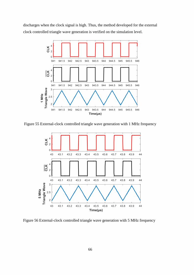
66
discharges when the clock signal is high. Thus, the method developed for the external
clock controlled triangle wave generation is verified on the simulation level.
Figure 55 External-clock controlled triangle wave generation with 1 MHz frequency
Figure 56 External-clock controlled triangle wave generation with 5 MHz frequency

67
4.2.2 Comparator
The comparator used in the PWM IC is required to compare the reference input signal
with the generated triangle wave. Two of the most used topologies used in the literature
are the static comparators and dynamic comparators. The static comparators can be
considered as continuous-mode comparators while the dynamic comparators as
clocked-mode comparators. The dynamic comparators are mostly used in A/D
converters and memory circuits, where continuous operation is not required [55]–[57]
[58]. In dynamic comparators, the comparison is only started when they are triggered
by a clock signal. By this way, low power circuits can be designed. On the other hand,
The static comparators are open-loop based implementations [59], [60].
Propagation delay of a comparator is a critical parameter that defines the speed of a
comparator. For a comparator used in PWM generation, the propagation delay should
be much smaller than the period of the PWM. As a rule of thumb, a ratio of (1/10)
yields a good design [8]. Another critical parameters are the open-loop gain, the slew
rate, and the input offset [61].
The two-stage OPAMP without compensation is a good candidate for a high speed
comparator if the power consumption is not a concern. It can provide high DC gain
and low input offset [58], [59], [62]. This circuit can tolerate small capacitive loads
but it will face slew-rate limitation when it is required to drive larger capacitive loads.
For this purpose, a further improvement can be applied to the two-stage comparator so
that larger capacitive load can be driven. Improvement of driving large capacitive
loads is provided with the tapered buffer topology [63], [64], [65]. The tapered buffer
is a circuit with a chain of inverter stages. Jaeger in [66] stated that minimum
propagation delay can be achieved for a tapered buffer if each transistor in a stage has
a width, where it is fixed multiple of that of transistors participated in the previous
stage. The ratio between the widths of the transistors in each stage is constant and it is
called as taper factor denoted as F. The idea of the N-stage tapered buffer is shown in
Figure 57.

68
Ci CL
Stage # # 0 # 1 # N-2 # N-1
1 FNFN-1F
Figure 57 N-stage tapered buffer
The equation for the taper factor is expressed as
𝐹 = (𝐶𝐿
𝐶𝑖)1/𝑁
, (25)
where Ci is the input capacitance of the first inverter (minimum size), CL is the load
capacitance, and N is the number of inverter stages. The tapered buffer is designed so
that it can drive capacitive loads up to 10 pF, where N=4 and F=6.
The schematic of the comparator with tapered buffer is illusturated in Figure 58. The
comparator has a tapered inverter at its output since the PWM and its complement are
required as the outputs of the PWM IC.
M2M1
M3
M5M8 M6
M7
IN-M9
M4
IN+
VDD
OUT
OUT
Figure 58 The circuit schematic of the comparator
Figure 59 shows the propagation delay simulation of the comparator. The circuit is
simulated for the worst case scenario, which is 5 MHz operation when it drives a
capacitive load of 10 pF. The delay is the time interval between the time instants of
(VIH+VIL)/2 and (VOH+VOL)/2, where VIH and VIL are the high and low levels of the
input voltage, and VIH and VIL are the high and low levels of the output voltage,

69
respectively. The propagation delay occurs at both low-to-high transition and high-to-
low transistions of the output. The propagation delay can be calculated by taking
average of the rising and the falling values. The average propagation delay is
calculated as 3.48 ns, which is much smaller than the lowest period of the desired
PWM operation (200 ns for 5 MHz PWM operation).
Figure 59 Propagation delay of the comparator
4.3 Layout
The full-chip layout of the presented PWM IC including the pad-frame is shown in
Figure 60.
Figure 60 The microphotograph of the PWM IC
triangle wave
generator
com
par
ator

70
In the layout of the PWM IC, common standard analog layout techniques have been
followed and implemented for obtaining better results. The device matching using
common-centroid layout techniques has been applied for the differential pair of the
OPAMPs, the transistors in the current mirror, etc. For improved performance, dummy
transistors and resistors are used in the layout design. In the band-gap reference, the
vertical npn transistors is selected as 1:15 (1:n) so that 4x4 array can be obtained for
better layout.
4.4 Top-level Simulations
The top-level simulations of the PWM IC have been performed with full-chip parasitic
extraction including pad frame and all bond-wire effects. The performance of the
PWM IC for 5 MHz operation is illustrated in this chapter since it is the most
challenging scenario for the PWM IC.
Figure 61 shows the 5 MHz PWM operation of the presented PWM IC with 500 kHz
sinusoidal input signal.
Figure 61 5 MHz operation of the PWM IC with 500 kHz sinusoidal input signal
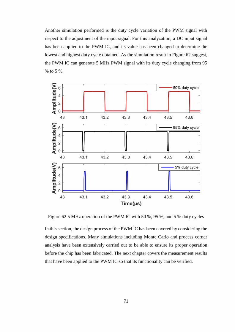
71
Another simulation performed is the duty cycle variation of the PWM signal with
respect to the adjustment of the input signal. For this analyzation, a DC input signal
has been applied to the PWM IC, and its value has been changed to determine the
lowest and highest duty cycle obtained. As the simulation result in Figure 62 suggest,
the PWM IC can generate 5 MHz PWM signal with its duty cycle changing from 95
% to 5 %.
Figure 62 5 MHz operation of the PWM IC with 50 %, 95 %, and 5 % duty cycles
In this section, the design process of the PWM IC has been covered by considering the
design specifications. Many simulations including Monte Carlo and process corner
analysis have been extensively carried out to be able to ensure its proper operation
before the chip has been fabricated. The next chapter covers the measurement results
that have been applied to the PWM IC so that its functionality can be verified.


73
CHAPTER V
PERFORMANCE EVALUATION BASED ON
EXPERIMENTAL RESULTS
The PWM IC presented in Chapter 4 has been fabricated in a commercial 0.35 µm
CMOS process. Figure 63 shows the microphotograph of the fabricated chip. The full-
chip area is 1.8 mm x 1.4 mm including the pad frame. All pads are ESD protected.
ESD rating of the chip is yet to be evaluated, but expected to be Class-2A or higher.
Figure 63 The microphotograph of the PWM IC
The integrated circuit packaging is an important step considering its effect on the
performance of the integrated circuit. The bonding wires, connecting the pads on the
die to the package pins, result in parasitic inductances. These bond-wires have large
impact on the performance of the circuits, especially when carrying high frequency,
high current switching signals. To minimize the parasitic effects of the wire-bonds, the
length of them should be kept as small as possible [67], [68]. Another parasitic

74
influence results from the leads of the package whose length should be reduced as well.
For the package of the presented PWM IC, Quad Flat No-Leads (QFN) package was
chosen. QFN packages offer minimized parasitics thanks to their leadless structure.
Another advantage of the QFN package is its exposed paddle, which is generally
connected to the ground plane of a PCB by metal vias. It brings improved thermal
performance acting as a heat sink by decreasing the thermal resistance [69]. Besides,
through the use of wire-bonds directly connected to the exposed paddle (a.k.a. down-
bonds), the QFN package helps reduce the total parasitic inductance of the circuit
ground plane. To keep other wire-bonds as short as possible, the smallest QFN package
that can accommodate the die was chosen. For this work, a 5 mm x 5 mm QFN package
with 16 pins shown in Figure 64 is used.
Figure 64 The fabricated PWM IC in the QFN package
In order to test the functionality of the presented PWM IC, a test printed circuit board
(PCB) was designed and fabricated. A picture of the test PCB populated with the PWM
IC and all necessary components is shown in Figure 65. It is a two-layer board with
the dimension of 5 cm x 5 cm x 1.6 mm. As its schematic can be seen in Figure 66, the

75
test PCB contains the supply voltage filtering part to filter out the AC components
from the DC voltage supply, and the PWM IC.
Figure 65 The test PCB for the PWM IC
CR
NT
_A
DJ
CL
K
PWM_P
PWM_N
VDD1
GND1
AN
LG
_IN
TR
IAN
GL
E
GN
D2
VD
D2
VDD
GND3
VDD3
SHLD
R1
35 KΩ
GND
external
clock signal
PWM signal
C8
1 uF
GND
5V_OUT
GND
PWM signal
analog
input signal
C9
GND
GND
C10
1 uF
GND
5V_OUT
C11
1 uF
GND
5V_OUT
GND
C12
1 uF
GND
5V_OUT GND
C1
100 uF
C2
22 uF
C3
100 nF
L1
bead
C7
100 uF
C5
4.7 uF
C6
22 uF
C4
100 nF
GND GND
5V_IN 5V_OUT
SUPPLY VOLTAGE FILTERING
PWM IC
Figure 66 The schematic of the test PCB

76
To correctly validate the performance of the PWM IC, it is important to design the test
PCB carefully by applying some design and layout rules. One is the decoupling on the
PCB level in addition the decoupling on the IC level. To decouple the high-frequency
noise in the supply pins of the PWM IC, decoupling ceramic capacitors C8, C10, C11,
and C12 have been used. It is critical to locate these capacitors very close to the IC’s
supply pins to minimize the self-inductance of the PCB trace. Another issue is the
ground connection. It is also required to make short connections from the ground pins
to the ground plane to be able to minimize the self-inductance due to the PCB traces.
A large ground plane prevents large voltage drops and satisfies all ground connections
having the same reference potential.
In order to measure the PWM IC, various tests were performed as will be detailed in
the following sub-sections. In all of these tests, the PWM IC was used to drive either
a single or a multitude of class D power amplifiers. These PAs are populated on the
same PCB as shown in Figure 67. As can be seen from the figure, Class D PAs are
proceeded by appropriate filtering constructed by L type networks. The design of these
networks is beyond the scope of this work and will not be explained. However, it is
sufficient to say that, they help to reconstruct the input signal by filtering out the
harmonics at the output of the PAs.
Figure 67 The test setup with required hardware
PWM IC Class D PA L network

77
Figure 68 shows all the test and measurement equipment for the measurement setup.
The DC supplies are used to provide power to the PWM IC and Class D PAs, the
function generators are used to generate the external clock and the PWM input coding
signal, and the scope is used is to plot the output waveforms.
Figure 68 The test setup with the required equipment
5.1 Triangle Wave Generation
The presented PWM IC has been tested for the evaluation of the clock-controlled
triangle wave generation. The measurement results for 1 MHz and 5 MHz operation
are shown in Figure 69 and 70, respectively. These results are taken by using a scope
and replotted on MATLAB software for better visualization. These measurement
results illustrate the external clock signal applied to the PWM IC, and the generated
triangle wave. As can be seen in Figure 69 and 70, the method developed for the
generation of the triangle wave with adjustable frequency is verified. When the
external clock signal is low, the charging of the off-chip capacitor occurs while the
discharging is enabled when the external clock signal is high. The measured peak-to-
peak amplitude of 1 MHz triangle wave is 980 mV and its DC offset is deviated by 30

78
mV from the ideal operation (2.5 V offset). On the other hand, 5 MHz triangle wave
has been generated with a peak-to-peak amplitude of 940 mV and its DC offset is
deviated by 80 mV from the ideal operation.
Figure 69 Triangle generation for 1 MHz operation
Figure 70 Triangle wave generation for 5 MHz frequency
Another test applied to the PWM IC is the validation of the synchronized triangle wave
generation. For this purpose, an external clock signal is applied to two PWM ICs and
the generated triangle waves of two chips is probed. Figure 71 shows two synchronized
2.89 V
1.95 V
2.96 V
1.98 V

79
triangle waves with a frequency of 5 MHz, and the time delay between two signals is
measured as 800 ps. Please note that a DC offset variation of 50 mV and a peak-to-
peak amplitude variation of 40 mV occur between two generated triangle waves, which
is related to component tolerances and process variations.
Figure 71 Synchronized triangle wave generation of two chips for 5 MHz
5.2 PWM Generation
The PWM generation has been tested for both AC and DC input signals. The PWM
operation with an AC input signal measurements have been performed by considering
the class D power amplifier applications. As we have covered in Chapter 3, DC-DC
converters use the PWM in their control loop so that they compare a DC error voltage
with a carrier signal to regulate their output voltage. Thus, the PWM operation with a
DC input signal has also been experimented. Besides, the operation with a DC input
signal has been used to determine the range of the duty cycle variation by adjusting
the DC input signal. The results are demonstrated for frequencies of 1 MHz and 5
MHz.
Figures 72 and 73 show the duty cycle variation of the PWM signal with respect to a
DC input signal. The top-level simulation of the PWM IC have suggested a duty cycle
variation range from 5% to 95% for up to 5 MHz frequency. On the other hand, the
measured applicable range of duty cycle variation for 1 MHz PWM operation is

80
between 8% to 92% while the measured values for 5 MHz PWM operation is between
20% to 80% as can be seen in Figures 72 and 73, respectively. The discrepancy is
related to the slew rate of the comparator. There are additional capacitive loading
effects at the output of the comparator, such as PCB traces, cable connections, and the
input capacitances of the probe. They all limit the capacitive load driving capability of
the comparator.
Figure 72 The duty cycle variation range for 1 MHz PWM operation
Figure 73 The duty cycle variation range for 5 MHz PWM operation

81
The PWM operation has also been tested for an AC input signal. Figure 74 shows the
results of 5 MHz PWM operation including a sinusoidal input signal with a frequency
of 1 MHz and a peak-to-peak amplitude of 200 mV. The PWM operation can be
roughly verified by this figure in such a way that the PWM signal switches from low
level to high level when the value of the triangle wave is greater than the value of the
input signal, and vise-versa. However, more detailed analysis on this data is required
to strengthen the verification of the PWM operation.
Figure 74 5 MHz PWM operation with a 1 MHz sinusoidal input signal
In order to evaluate the performance of the PWM generation fully, it is required to
examine the frequency content of the generated PWM signal. For a sinusoidal input
signal as in (6), where it consists of both AC and DC components, a PWM signal with
a peak-to-peak amplitude VPWM,pp should a fundamental component with an amplitude
of
𝑉𝑃𝑊𝑀,𝑝𝑝 × (𝑅1
𝐶𝑚), (26)
where R1 is the amplitude of the input signal and Cm is the peak-to-peak amplitude of
the generated triangle wave. Considering the case in Figure 74, the ideal operation
requires a fundamental component with an amplitude of 0.5 V since Cm is set to 1 V,
VPWM,pp is 5 V, and R1 is equal to 0.1 V. For better evaluation, the measured result is
compared with the ideal case implemented in MATLAB software. Figure 75 shows

82
the amplitude spectrum comparison of the generated and the ideal PWM signals for
the case in Figure 74. The amplitude of the fundamental component is 0.53 V, which
is larger than the 0.5 V because the generated triangle wave has a peak-to-peak
amplitude less than 1 V compared to the ideal case. Another important observation is
related to the IM harmonics at the frequency of 4 MHz. For the ideal operation, the IM
at the frequency of 4 MHz is zero as expected while there is a harmonic component in
practice due to the deviation in the peak-to-peak amplitude of the generated the triangle
wave compared to the ideal case. However, these IM harmonics are not problematic
in the operation since they are away from the fundamental component thanks to the
high frequency operation. Thus, they can be filtered out with appropriate filtering.
Figure 75 Spectral analysis of the PWM operation in Figure 74
Another measurement has been configured to be able to validate the synchronized
performance of the PWM IC. For this purpose, an external clock signal with a
frequency of 5 MHz and a coding input signal of 500 kHz have been connected to two
PWM ICs while the generated PWM signals have been probed. To analyze the results,

83
the generated PWM signals have been digitally filtered in MATLAB software and the
time delay between the modulated inputs signals have been measured. Figure 76
illustrates the filtered PWM signals generated by two synchronized PWM ICs. The
time delay between the two signals is measured as 4.8 ns, where this value is specified
as 5.5 ns in the design specifications. Please note that there is a deviation of 13 mV in
the peak-to-peak amplitudes of two signals, which is related to the component
tolerances and the process variations.
Figure 76 The filtered PWM signals of two PWM ICs in synchronized operation
The propagation delay of the PWM IC is another parameter that have been measured.
Figure 77 shows the result of propagation delay measurement, where the PWM
frequency is set to 5 MHz and the input signal is arranged to a DC value of 2.5 V. The
rising-edge propagation delay is measured as 15.6 ns and the falling-edge propagation
delay is measured as 22 ns, where the simulation values are 2.98 ns and 3.98 ns,
respectively for 10 pf capacitive load. This deviation is related to the extra capacitive
loading, which limits the slew rate of the comparator. On the other hand, the average
propagation delay is measured as 18.8 ns, which is much smaller (1/10) than the period
of the 5 MHz PWM signal.

84
Figure 77 Propagation delay measurement of the PWM IC for 5 MHz operation
Another design specification for the PWM IC is the generation of the PWM signal and
its complement up to 5 MHz frequency. Figures 78 and 79 show the PWM and its
complement generation for 5 MHz and 1 MHz, respectively. The major difference
between the 1 MHz and 5 MHz operations is that the PWM IC falls short in slew rate
for 5 MHz operation compared to 1 MHz operation.
Figure 78 PWM signal and its complement for 5 MHz frequency

85
Figure 79 PWM signal and its complement for 1 MHz frequency
5.3 Integration with the Class D Power Amplifier
The integration of the PWM IC with a class D power amplifier has been established
and a resistive load has been connected to the output of the class D power amplifier.
The class D power amplifier has an L type network, which is a matching circuit
consisting of an inductor and a capacitor. It can provide filtering since it is a resonant
circuit and it has a band-pass filter shape frequency response. The design of the L type
network and the class D power amplifier are not covered in this work.
The PWM frequency is set to 5 MHz and a single-tone sinusoidal input signal with a
frequency of 500 kHz is applied to the PWM IC. The operation of the class D power
amplifier has been observed for the input signals with the peak-to-peak amplitudes of
100 mV, 200 mV, and 400 mV. It is verified that the output of the class D power
amplifier performs a linear increase as the peak-to-peak amplitude of the input signal
is doubled as can be seen in Figure 80.

86
Figure 80 The output of the Class D power amplifier for an input signal with
different amplitudes
To be able to validate the external synchronization capability of the PWM IC in a class
D power amplifier, a measurement setup has been arranged with two identical PWM
ICs and class D power amplifiers as can be seen in Figure 67. The outputs (both PWM
signal and its complement) of the two PWM ICs, which are both driven by the same
external clock signal are connected to the PWM inputs of the two identical class D
power amplifier circuits. The PWM frequency is set to 5 MHz by adjusting the external
clock signal. A sinusoidal input signal with a frequency of 500 kHz is applied to the
both PWM ICs. The class D power amplifiers have two identical L type networks so
that the filtered input signals can be obtained and the time-delay between them can be
measured.
Figure 81 shows the outputs of the two class D power amplifiers, which are
synchronized by the PWM IC. The time delay between these two signals is measured
as 8.9 ns. In addition to the time delay related to the PWM IC, the sources for the time
delay between the outputs of the class D power amplifiers can be listed as component
tolerances on both L-networks and class D power amplifiers, PCB trace mismatches,
and cable connections.
10.8 V
5.3 V
2.6 V
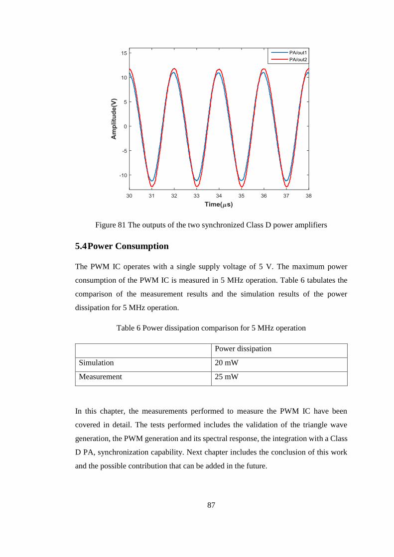
87
Figure 81 The outputs of the two synchronized Class D power amplifiers
5.4 Power Consumption
The PWM IC operates with a single supply voltage of 5 V. The maximum power
consumption of the PWM IC is measured in 5 MHz operation. Table 6 tabulates the
comparison of the measurement results and the simulation results of the power
dissipation for 5 MHz operation.
Table 6 Power dissipation comparison for 5 MHz operation
Power dissipation
Simulation 20 mW
Measurement 25 mW
In this chapter, the measurements performed to measure the PWM IC have been
covered in detail. The tests performed includes the validation of the triangle wave
generation, the PWM generation and its spectral response, the integration with a Class
D PA, synchronization capability. Next chapter includes the conclusion of this work
and the possible contribution that can be added in the future.


89
CHAPTER VI
CONCLUSION AND FUTURE WORK
6.1 Conclusion
In this thesis, the design and implementation of an analog high frequency pulse width
modulation integrated circuit is presented. The chip is fabricated in a commercial 0.35
µm CMOS process. The selection of sampling method as the natural sampling offers
excellent spectral response. Besides, this architecture uses an analog triangle wave as
the carrier signal to provide small harmonic distortion. Its analog nature also offers
higher resolution and less quantization error compared to the digital implementations.
The PWM IC generates a maximum of 5 MHz user adjustable PWM signal and its
complement. It employs an external clock controlled architecture so that it allows the
multitude of chips to operate in synchronization. Based on the results of the presented
work, the following conclusions and comments can be drawn:
1. Generating the triangle wave with respect to an external clock signal is verified.
The charging and the discharging cycles of an off-chip capacitor is successfully
controlled by the external clock signal. By this way, the triangle wave with
adjustable frequency is obtained, which results in frequency adjustable PWM
operation.
2. In synchronized operation at 5 MHz frequency, the skew error between the
triangle waves is measured as 800 ps, which includes variation due to the
component tolerances, mismatches in the cable connections, and PCB related
deviations.
3. The time delay between two coded AC input signals with up to 500 kHz
frequency is measured as 4.8 ns at the output of the PWM IC. This value is
90
lower than the specified value, which is 5.5 ns corresponding to a phase shift
of 1° in a phased array system at 500 kHz operation frequency.
4. The integration of the PWM IC and the class D PA has been verified for 5 MHz
PWM and 500 kHz sinusoidal input signal. In the first test configuration, a
single PWM IC has driven a single class D PA. In this test, the amplitude of
the 500 kHz input signal is doubled for three different values and, the rise in
the output voltage amplitude of the PA has been successfully observed. For the
second test, two PWM ICs have been synchronized by an external clock signal
so that the skew error between the output signals of the class D PAs have been
observed. The skew is measured as 8.9 ns, which can further be reduced by
minimizing the mismatch sources in the system such as cable connections and
PCB layout of the class D PAs.
5. The measured average propagation delay at the output of the PWM for 5 MHz
operation is 18.8 ns. This value is much smaller than the period of 200ns (5
MHz frequency), which corresponds to the most challenging condition of the
PWM IC. The measured values are larger than the simulation results due to
capacitive loading effects mostly in the PCB traces and cables, which are not
taken into account during simulations.
6. The measured applicable duty cycle variation range is from 20% to 80% for 5
MHz PWM operation, and from 8 % to 92% for 1 MHz PWM operation. The
decrease in the ranges between 1 MHz and 5 MHz occurs due to the slew-rate
limitation of the comparator. In practice, the output of the comparator faces
with extra capacitive loading effects, such as PCB traces, cables, the
measurement signal probe. Minimizing these capacitive sources will yield
better results.
7. In the triangle wave generation, there is around 50 mV deviation in the peak-
to-peak amplitude, and the DC offset of the triangle wave from the ideal case
due to the process variations and the component tolerances. Due this
discrepancy, the PWM IC falls short in terms of cancellation of the first order
IM harmonics (m=1, n=±1). However, this situation can be overcome thanks
to the high frequency operation. These harmonics can easily be filtered out so
that they do not result in the harmonics distortion at the output of the class D
PA.

91
A performance comparison between the presented PWM IC and other analog-based
implementations can be made. The digital implementations are excluded from the
comparison since they suffer from low resolution.
As can be seen in Table 7, LTC6692 of Linear Technology, USA [9] is the closest
alternative of the PWM IC presented in this work. Its major advantage over the
proposed PWM IC is its duty cycle variation range. On the other hand, it suffers from
the frequency error since the frequency is set by an off-chip resistor. Besides, its
maximum PWM frequency is 1 MHz, and it falls short compared to the PWM IC in
terms of the external synchronization ability.
Table 7 The comparison of analog-based pulse width modulators
Pulse Width
Modulator
Circuit
Type
Operating
Frequency
External
Synchronization
Duty Cycle
Variation (1 MHz)
[8] Discrete 500 kHz None -
[9] Integrated 1 MHz None 0% - 100%
Proposed Work Integrated 5 MHz Yes 8% - 92%
In conclusion, the analog high frequency PWM generation, and the external clock-
controlled architecture of the presented PWM IC make it be a strong candidate in
PWM-based applications such as the switch-mode power supplies and the class D
power amplifiers.
6.2 Future Work
In this thesis, an analog high frequency pulse width modulation integrated circuit with
external clock synchronization capability is implemented by satisfying many of its
specifications. As a future work, the design of the comparator can be revised to be able
to increase its slew rate so that the duty cycle variation range can be increased. Besides,
a trimming structure can be added to the circuit to minimize the process variation
dependence of the generated triangle wave.
For further improvement of the presented PWM IC, a digital-to-analog converter
(DAC) circuit can be designed as the digital front-end. Most of the SONAR systems

92
employ special signals such as linear frequency modulated (LFM) and hyperbolic
frequency modulated (HFM) to locate and classify the underwater targets. These
signals are usually generated in an FPGA or a DSP. Thus, with the development of an
integrated DAC, the PWM IC will have a digital interface, which brings an important
simplicity to the systems.

93
REFERENCES
[1] A. Bindra, “Pulsewidth Modulated Controller Integrated Circuit: Four Decades
of Progress [A Look Back],” IEEE Power Electron. Mag., vol. 1, no. 3, pp. 10–
44, 2014.
[2] J. M. Rivas, D. Jackson, O. Leitermann, A. D. Sagneri, and D. J. Perreault,
“Design Considerations for Very High Frequency dc-dc Converters,” 37th
IEEE Power Electron. Spec. Conf., pp. 1–11, 2006.
[3] D. Y. Lee, B. K. Lee, and D. S. Hyun, “Novel Full-Bridge Zero-Voltage-
Transition PWM DC/DC converter with zero-voltage/zero-current switching of
the auxiliary switches,” PESC Rec. IEEE Annu. Power Electron. Spec. Conf.,
vol. 2, 1998.
[4] J. Wittmann and B. Wicht, “MHz-converter design for high conversion ratio,”
Proc. Int. Symp. Power Semicond. Devices ICs, pp. 127–130, 2013.
[5] E. Koutroulis, A. Dollas, and K. Kalaitzakis, “High-frequency pulse width
modulation implementation using FPGA and CPLD ICs,” J. Syst. Archit., vol.
52, no. 6, pp. 332–344, 2006.
[6] X. Gong, “A digital audio amplifier using pulse width modulation for portable
applications,” Ph.D. dissertation, Dept. Elect. Comput. Eng., Uni. of Florida,
Gainesville, FL, 2007.
[7] J. Lu, H. Song, and R. Gharpurey, “A CMOS class-D line driver employing a
phase-locked loop based PWM generator,” IEEE J. Solid-State Circuits, vol.
49, no. 3, pp. 729–739, 2014.
[8] Texas Instruments, “TI Precision Designs : Verified Design Analog Pulse
Width Modulation,” TIPD108 datasheet, Jun., 2013.
[9] Linear Technology Corporation, “Voltage-Controlled Pulse Width Modulator
(PWM),” LTC6692 datasheet, 2010.

94
[10] M. K. Kazimierczuk, "Topologies of PWM DC-DC converters," in Pulse-width
Modulated DC-DC Power Converters, UK: Wiley, 2008, pp. 16-18.
[11] S. J. Chapman, "Pulse-width modulation inverters," in Electric Machinaery
Fundamentals, New York: McGraw-Hill, 2003, pp. 203-205.
[12] G. Franzo, M. Mazzucchelli, L. Puglisi, and G. Sciutto, “Analysis of PWM
Techniques Using Uniform Sampling in Variable-Speed Electrical Drives with
Large Speed Range,” IEEE Trans. Ind. Appl., vol. IA-21, no. 4, pp. 966–974,
1985.
[13] Hitex RCD USA, HS-322HD Standard Heavy Duty Servo [Online]. Available:
http://hitecrcd.com/products/servos/sport-servos/analog-sport-servos/hs-
322hd-standard-heavy-duty-servo/product
[14] M. Ned, M.U.Tore, and P.R.William, Power Electronics Converters,
Applications, and Design. New York: Wiley, 2003.
[15] M. Jovanović, “Power supply technology–Past, present, and future,” Power
Convers. Intell. Motion China Conf. (PCIM China), pp. 3–15, 2007.
[16] A. S. Sedra and K. C. Smith, Microelectronics Circuits, New York: Oxford
Press, 2004.
[17] X. Lurton, An Introduction to Underwater Acoustics. Springer Science Business
Media, 2002.
[18] C. H. Yun, N. Y. Ko, Y. S. Moon, and H. T. Choi, “Design and experiment of
an acoustic transducer for underwater navigation,” Ocean. 2014 - Taipei, pp. 1–
5, 2014.
[19] G. R. Walker, “Digitally-Implemented Naturally Sampled PWM Suitable for
Multilevel Converter Control,” IEEE Trans. Power Electron., vol. 18, no. 6, pp.
1322–1329, 2003.
[20] F. Vasca and L. Iannelli, Dynamics and Control of Switched Electronic Systems,
Springer, 2013.

95
[21] P. H. Mellor, S. P. Leigh, and B. M. G. Cheetham, “Reduction of spectral
distortion in class D amplifiers by an enhanced pulse width modulation
sampling process,” Circuits, Devices Syst. IEE Proc. G, vol. 138, no. 4, pp. 441–
448, 1991.
[22] K. Nielsen, “A review and comparison of pulse width modulation (PWM)
methods for analog and digital switching power amplifiers,” 1997.
[23] Z. Song and D. V Sarwate, “The frequency spectrum of pulse width modulated
signals,” Signal Processing, vol. 83, no. 4, pp. 2227-2258, 2003.
[24] Z. Kulka, “Application of pulse modulation techniques for class-D audio power
amplifiers,” Archives of Acoustics, vol. 706, pp. 683–706, 2007.
[25] A. V. Peterchev, J. Xiao, and S. R. Sanders, “Architecture and IC
implementation of a digital VRM controller,” IEEE Trans. Power Electron.,
vol. 18, no. 1, pp. 356–364, 2003.
[26] T. Takayama and D. Maksimovic, “Digitally controlled 10 MHz monolithic
buck converter,” Proc. IEEE Work. Comput. Power Electron. COMPEL, pp.
154–158, 2006.
[27] A. V Peterchev, S. Member, and S. R. Sanders, “Quantization resolution and
limit cycling in digitally controlled PWM converters,” IEEE Trans. Power
Electron., vol. 18, no. 1, pp. 301–308, 2003.
[28] M. L. Torregoza, E. R. Magsino, and J. C. Cabiles-Magsino, “Effects of
quantization on digital buck converter switch mode power supply,” J. Autom.
Control Eng., vol. 2, no. 2, pp. 154–159, 2014.
[29] Y. Qiu, J. Li, M. Xu, D. S. Ha, and F. C. Lee, “Proposed DPWM scheme with
improved resolution for switching power converters,” IEEE Ann. Applied
Power Electron. Conf., no. 1, pp. 1588–1593, 2007.
[30] G. Y. Wei and M. Horowitz, “A low power switching power supply for self-
clocked systems,” Proc. Int. Symp. Low Power Electron. Design, pp. 313–317,
1996.

96
[31] M. G. Y. Batarseh, “Digital pulse width modulator techniques for DC–DC
converters,” Ph.D dissertation, Dept. of Elect. and Compt., Uni. of Central
Florida, Orlando, FL, 2010.
[32] P. Wong and F. C. Lee, “Switching action delays in voltage regulator modules
,” pp. 675–678, 2002.
[33] W. Qiu, G. Miller, G. Z. Liang, and S. C. Drive, “Dual-edge pulse width
modulation scheme for fast transient response of multiple-phase voltage
regulators,” pp. 1563–1569, 2007.
[34] V. Yousefzadeh, T. Takayama, and D. Maksimovi, “Hybrid DPWM with digital
delay-locked loop,” Proc. IEEE Work. Comput. Power Electron. COMPEL, pp.
142–148, 2006.
[35] P. C. Sen, “Digital control of switching power converters,” Proc. 2005 IEEE
Conf. Control Appl. 2005. CCA 2005., pp. 635–640, 2005.
[36] J. Li et al., “High resolution digital duty cycle modulation schemes for voltage
regulators,” APEC 07 - Twenty-Second Annu. IEEE Appl. Power Electron.
Conf. Expo., pp. 871–876, 2007.
[37] S. Chander, P. Agarwal, and I. Gupta, “ASIC and FPGA based DPWM
architectures for single-phase and single-output DC-DC converter: a review,”
Open Eng., vol. 3, no. 4, pp. 620–643, 2013.
[38] T. Vekslender, E. Abramov, Y. Bezdenezhnykh, A. Cervera, and M. M. Peretz,
“Full IC design of a PWM controller with integrated high-resolution ADC and
DPWM peripherals using digital backend tools,” 2014 IEEE 28th Conv. Electr.
Electron. Eng. Isr. IEEEI 2014, 2014.
[39] B. J. Patella, A. Prodić, A. Zirger, and D. Maksimović, “High-frequency digital
PWM controller IC for DC-DC converters,” IEEE Trans. Power Electron., vol.
18, no. 1, pp. 438–446, 2003.

97
[40] R. F. Foley, R. C. Kavanagh, W. P. Marnane, and M. G. Egan, “A versatile
digital pulsewidth modulation architecture with area-efficient FPGA
implementation,” IEEE 36th Conf. Power Electron. Spec. 2005., pp. 2609–
2615, 2005.
[41] X. Li and T. Xu, “A high-resolution hybrid DPWM circuit for digitally
controlled buck converter in 0.13 um CMOS process,” Int. Proc. Comput. Sci.,
vol. 51, pp. 670–676, 2012.
[42] X. Shen, X. Wu, J. Lu, and L. Qin, “Hybrid DPWM with analog delay locked
loop,” Int. Multiconference Eng. Comput. Sci., vol. II, pp. 1279–1281, 2010.
[43] A. Syed, E. Ahmed, D. Maksimović, and E. Alarcón, “Digital pulse width
modulator architectures,” PESC Rec. - IEEE Annu. Power Electron. Spec.
Conf., vol. 6, pp. 4689–4695, 2004.
[44] C. Pa, K. Cho, S. Member, R. Gharpurey, and S. Member, “A 40 – 170 MHz
PLL-Based PWM Driver Using,” IEEE J. Solid-State Circuits, vol. 51, no. 11,
pp. 2639-2650, 2016
[45] R. Choudhary, M. Bhardwaj, and P. B. P. Singh, “Design and Analysis of Pulse
width Modulator ( PWM ) using Current Comparator,” Int. J. Sci. Eng. Res.,
vol. 3, no. 5, pp. 1–8, 2012.
[46] M. G. Batarseh, W. Al-Hoor, L. Huang, C. Iannello, and I. Batarseh, “Window-
masked segmented digital clock manager-FPGA-based digital pulsewidth
modulator technique,” IEEE Trans. Power Electron., vol. 24, no. 11, pp. 2649–
2660, 2009.
[47] Silicon Labs, “Class D audio driver with precision dead-time generator.”
Si824x datasheet, 2014.
[48] Maxim Integrated, “MAX15019 125V/3A, high-speed, half-bridge MOSFET
drivers datasheet,” MAX15018/9 datasheet, 2008.
[49] B.Razavi, Design of Analog CMOS integrated Circuits. New York: McGraw-
Hill, 2001.

98
[50] Y. P. Tsividis and R. W. Ulmer, “A CMOS voltage reference,” IEEE J. Solid-
State Circuits, vol. 13, no. 6, pp. 774–778, 1978.
[51] P. R. Gray, P. J. Hurst, S. H. Lewis, and R. G. Meyer, “Analysis and Design of
Analog Integrated Circuits,” New York: Wiley, 2001.
[52] H. Banba et al., “A CMOS bandgap reference circuit with sub-1-V operation,”
IEEE J. Solid-State Circuits, vol. 34, no. 5, pp. 670–674, 1999.
[53] T. Kevin, “Sub-1V curvature compensated bandgap reference,” 3rd IEEE Int.
Workshop on Electronic Design, Test and Applications, pp. 4, 2004.
[54] Vishay, “Thin film precision thin film non-magnetic resistor.” Thin film resistor
datasheet, 2014.
[55] Y. L. Wong, M. H. Cohen, and P. A. Abshire, “A 1.2-GHz comparator with
adaptable offset in 0.35 um CMOS,” Circuits Syst. I Regul. Pap. IEEE Trans.,
vol. 55, no. 9, pp. 2584–2594, 2008.
[56] M. B. Guermaz, L. Bouzerara, A. Slimane, M. T. Belaroussi, B. Lehouidi, and
R. Zirmi, “High speed low power CMOS comparator for pipeline ADCs,” in
2006 25th Int. Conf. on Microelectronics, pp. 14–17, 2006.
[57] J. Tomisawa, K. Nishikawa, and S. Yamakawa, “Low-current consumption
CMOS comparator using charge-storage amplifier for A/D converters,” in Proc.
IEEE Int. Symp. on Circuits and Systems, 2008, pp. 1942–1945.
[58] B. J. McCarroll, C. G. Sodini, and H. S. Lee, “A high-speed CMOS comparator
for use in an ADC,” IEEE J. Solid-State Circuits, vol. 23, no. 1, pp. 159–165,
1988.
[59] S. Yewale and R. Gamad, “Design of low power and high speed CMOS
comparator for A/D converter application,” Wirel. Eng. Technol., pp. 90–95,
2012.
[60] V. Milovanovic and H. Zimmermann, “A two-differential-input/differential-
output fully complementary self-biased open-loop analog voltage comparator
in 40 nm LP CMOS,” Proc. Int. Conf. Microelectron. ICM, pp. 355–358, 2014.

99
[61] P. E. Allen and D. R. Holberg, CMOS Analog Circuit Design, 2nd ed. Oxford,
2007.
[62] D. N. Donadkar and S. U. Bhandari, “Review on comparator design for high
speed ADCs,” Proc.1st Int. Conf. Comput. Commun. Control Autom. ICCUBEA
2015, pp. 974–978, 2015.
[63] B. S. Cherkauer and E. G. Friedman, “A unified design methodology for CMOS
tapered buffers,” IEEE Trans. Very Large Scale Integr. Syst., vol. 3, no. 1, pp.
99–111, 1995.
[64] J. S. Choi and K. Lee, “Design of CMOS tapered buffer for minimum power-
delay product,” IEEE J. Solid-State Circuits, vol. 29, no. 9, pp. 1142–1145,
1994.
[65] S. L. Wong and C. A. T. Salama, “An efficient CMOS buffer for driving large
capacitive loads,” IEEE J. Solid-State Circuits, vol. 21, no. 3, pp. 464–469,
1986.
[66] R. C. Jaeger, “Comments on ‘An Optimized Stage for MOS Integrated
Circuits,’” IEEE J. Solid-State Circuits, no. 7, pp. 185–186, 1975.
[67] K. B. Unchwaniwala and M. F. Caggiano, “Electrical analysis of IC packaging
with emphasis on different ball grid array packages,” 2001 Proceedings. 51st
Electron. Components Technol. Conf., pp. 1496–1501, 2001.
[68] S. K. Yun and H. Y. Lee, “Parasitic impedance analysis of double bonding wires
for high-frequency integrated circuit packaging,” IEEE Microw. Guid. Wave
Lett., vol. 5, no. 9, pp. 296–298, 1995.
[69] M. J. Chen and S. A. Tabatabaei, “Broadband, quad flat no-lead (QFN) package
developed using standard overmold leadframe technology,” IEEE MTT-S Int.
Microw. Symp. Dig., pp. 457–460, 2010.