The Dark Side of Loop Control Theory...What is the Purpose of this Seminar? There have been numerous...
143
1 • Chris Basso – APEC 2012 The Dark Side of Loop Control Theory Christophe Basso IEEE Senior Member
Transcript of The Dark Side of Loop Control Theory...What is the Purpose of this Seminar? There have been numerous...

1 • Chris Basso – APEC 2012
The Dark Side of Loop Control Theory
Christophe Basso
IEEE Senior Member
Course Agenda
Introduction to Control Systems
Shaping the Error Signal
How to Implement the PID Block?
The PID at Work with a Buck Converter
Considering the Output Impedance
2 • Chris Basso – APEC 2012
Considering the Output Impedance
Classical Poles/Zeros Placement
Shaping the Output Impedance
Quality Factor and Phase Margin
What is Delay Margin?
Gain Margin is not Enough

What is the Purpose of this Seminar?
There have been numerous seminars on control loop theory
Seminars are usually highly theoretical – link to the market?
Control theory is a vast territory: you don't need to know everything!
This 3-hour seminar will shed light on some of the less covered topics:
PID compensators and classical poles/zeros compensation
3 • Chris Basso – APEC 2012
PID compensators and classical poles/zeros compensation
Output impedance considerations in a switching regulator
Understanding delay and modulus margins
In a 3-hour course, we are just scratching the surface…!
Course Agenda
Introduction to Control Systems
Shaping the Error Signal
How to Implement the PID Block?
The PID at Work with a Buck Converter
Considering the Output Impedance
4 • Chris Basso – APEC 2012
Considering the Output Impedance
Classical Poles/Zeros Placement
Shaping the Output Impedance
Quality Factor and Phase Margin
What is Delay Margin?
Gain Margin is not Enough

What is a Closed-Loop System?
A closed-loop system forces a variable to follow a setpoint
The setpoint is the input, the controlled variable is the output
French term is "enslavement": the output is slave to the input
A car steering wheel is a possible example:
5 • Chris Basso – APEC 2012
u t y t
control
The input u The output y
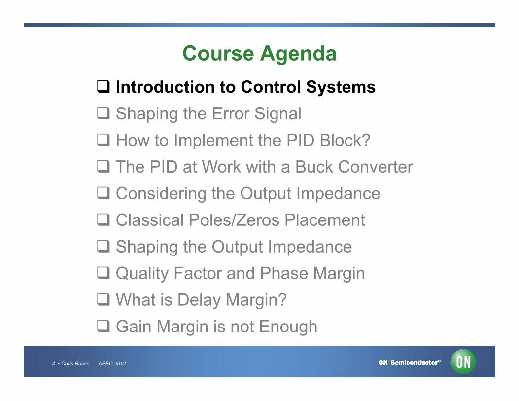
Representing a Closed-Loop System
A closed-loop system can be represented by blocks
The output is monitored and compared to the input
Error processing
+
-
sensor
°
° V
vc
6 • Chris Basso – APEC 2012
processing
Any deviation between the two gives birth to an error
This error is amplified and drives a corrective action
- V° V
The plantH
The compensatorG

A Servomechanism or a Regulator?
Airplane elevator control is a servoservo--mechanismmechanism:
• The pilot imposes a mechanical position via the yoke
u t
y tVariablesetpoint
7 • Chris Basso – APEC 2012
Car cruise control is a regulatorregulator:
• The speed is set, the car keeps it constant despite wind, etc.
v
u t constantv
setpoint
Fixedsetpoint
Output followsthe input
Output is constant

Processing the Error Signal
The error signal is processed through the compensator G
We want the following operating characteristics:
Speed
Precision
Robustness1.00
1.40
overshoot precision u t
8 • Chris Basso – APEC 2012
12.0u 36.0u 60.0u 84.0u 108u
-200m
200m
600m
speed
PID
Since1930
y t
Course Agenda
Introduction to Control Systems
Shaping the Error Signal
How to Implement the PID Block?
The PID at Work with a Buck Converter
Considering the Output Impedance
9 • Chris Basso – APEC 2012
Considering the Output Impedance
Classical Poles/Zeros Placement
Shaping the Output Impedance
Quality Factor and Phase Margin
What is Delay Margin?
Gain Margin is not Enough
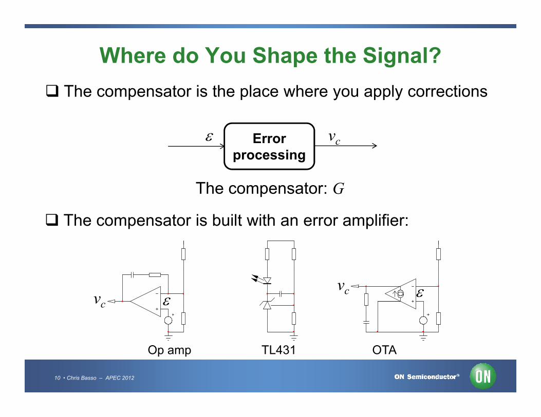
Where do You Shape the Signal?
The compensator is the place where you apply corrections
Error processing
The compensator: G
vc
10 • Chris Basso – APEC 2012
The compensator is built with an error amplifier:
Op amp TL431 OTA
vc vc

The PID Compensator
A PPID welcomes a Proportional block
c pv t k tpk t
240m
v t k is high: 248 mV
11 • Chris Basso – APEC 2012
4.29u 12.9u 21.5u 30.1u 38.7u
0
120m
t
cv t
2.48pk
kp is high:
reaction speed risks of overshoot
kp is low:
sluggish response
100 mV
248 mV

The PID Compensator
A PIID includes an Integrating block
0
tp
ci
kv t d
p
i
k
-2.92240m
v t Integral action:
t
12 • Chris Basso – APEC 2012
8.59u 25.8u 42.9u 60.1u 77.3u
-3.00
-2.98
-2.96
-2.94
0
120m
t
cv t Integral action:
no static error slow response decreases stability large overshoots
107μsi
-100 µV
-100u . 30k = -3 V
i
S

The PID Compensator
A PIDD offers a Derivative block
Derivative action:
c p d
d tv t k
dt
p d
dk
dt t
2.00240m 1.63Vp dk S
13 • Chris Basso – APEC 2012
Derivative action:
perturbation variationis known: anticipation stabilizes the responseo no static effect
3.66u 11.0u 18.3u 25.6u 32.9u
-2.00
-1.00
0
1.00
0
120m
t
cv t
1.63Vp dk S
163μsd
S

The PID Compensator
The Derivative block anticipates the signal evolution and speed
t
y
dt
t S
d
d
t tt
t
t
14 • Chris Basso – APEC 2012
tt dt
t
nowlater
d d
d tt t
dt
if smalld

Combining the Blocks
You can formulate the PID transfer function in different ways:
differentiation:
integration:
c c
d tv t V s s s
dt
c c
sv t t dt V s
s
The standard form:
1 The derivative term cannot
15 • Chris Basso – APEC 2012
1
1p di
G s k ss
The parallel form:
ip d
kG s k sk
s
be physically implemented:
lim ds
s
Need a pole
1
dd
d
ss
s
N

Combining the Blocks
The transfer function becomes a filtered PID:
1
1
1
dp
di
sG s k
ss
N
If we develop, we obtain a more familiar expression:
16 • Chris Basso – APEC 2012
If we develop, we obtain a more familiar expression:
21
1
d d ii d i
i d
p
s sN N
G s
s sk N
A double zeroAn origin poleA high-frequency pole
Course Agenda
Introduction to Control Systems
Shaping the Error Signal
How to Implement the PID Block?
The PID at Work with a Buck Converter
Considering the Output Impedance
17 • Chris Basso – APEC 2012
Considering the Output Impedance
Classical Poles/Zeros Placement
Shaping the Output Impedance
Quality Factor and Phase Margin
What is Delay Margin?
Gain Margin is not Enough

Practical Implementation
Sum up the output of each individual block:
pkP
Ipk
+
u(t)
(t)vc(t)
18 • Chris Basso – APEC 2012
Ii
D p d
dk
dt
-
y(t)
vc(t)
This is the parallel form of the PID

Practical Implementation
pkPI1
+
u(t)
(t) vc(t)
This is the filtered standard form of the PID
19 • Chris Basso – APEC 2012
pkPIi
D
-
y(t)
vc(t)
1
1 ds Nd
d
dt

Bridging a PID to a Type 3
A type 3 is implemented around an op amp
1 2
1 2
1 1
1 1
z z
po p p
s sG s
s s s
20 • Chris Basso – APEC 2012
1 2 2
1 2
2
1
1 1 11
1 1
z z z z
po p p
s s
G ss s s
Addedpole
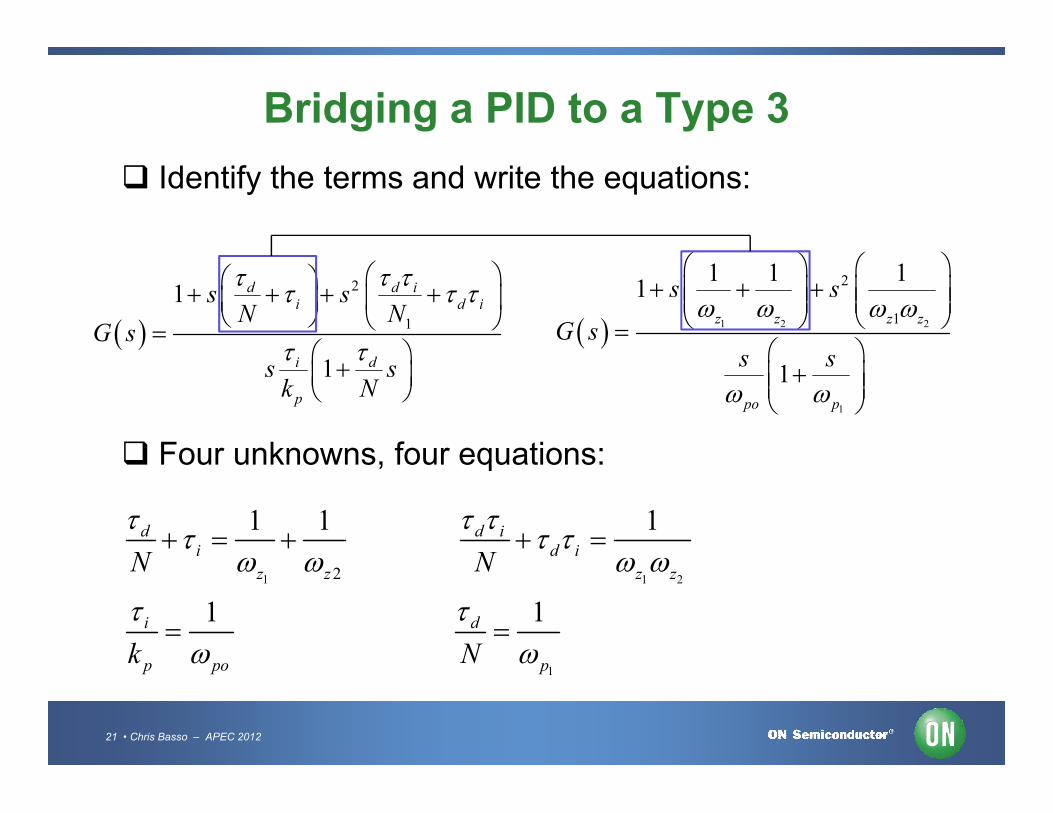
Bridging a PID to a Type 3
Identify the terms and write the equations:
1 2 2
1
2
1
1 1 11
1
z z z z
po p
s s
G ss s
2
1
1
1
d d ii d i
i d
p
s sN N
G s
s sk N
21 • Chris Basso – APEC 2012
1 1 2
1
2
1 1 1
1 1
d d ii d i
z z z z
i d
p po p
N N
k N
1po p p
Four unknowns, four equations:

Bridging a PID to a Type 3
From Type 3 to PID:
1 1 1 2
1 1 1 2 1 2 1
p z p z
d
p z p z z z p
1
1 1 1 2 1 2
2
1p
p z p z z z
N
1 2
1 2 1
1z z
i
z z p
1 1 2
po po po
p
z p z
k
22 • Chris Basso – APEC 2012
1 2 1z z p 1 1 2z p z
From PID to Type 3:
1
2 2 2 24 2
2 1 2
d d i i d i d i
z
d i
N N N Nf
N
2
2 2 2 24 2
2 1 2
d d i i d i d i
z
d i
N N N Nf
N
1 2p
d
Nf
2
p
po
i
kf

Testing the Conversion
Assume a type 3 compensator calculated for:
2740 Hzcf 1cf
G
1200 Hzzf
2600 Hzzf
121400 Hzpf
221400 Hzpf
2 2
f f
High-frequencypole
at a crossover of
The "0-dB crossover" pole is placed at:
23 • Chris Basso – APEC 2012
1 2
1
1
2
2 2
22
1 1
43.4 Hz 272 rd s
1 1
c
c c
p p
po f z
z c
c z
f f
f ff G f
f f
f f
194d u 1.05i m 25.6N 0.287pk

What is the "0-dB Crossover" Pole? s appears as an isolated term in N(s), it is an origin pole
1
1
1 p
G ss s
s = 0 is the origin pole
If s is affected by a coefficient it is the "0-dB crossover pole"
1
11 11
zz zz z po
ss s
s s s ss s s
24 • Chris Basso – APEC 2012
1 11 1
11 1 11
0
1 11
1 1 11
z zz z po
zp p pp
po
s s s ss s sG s G
sAs s s ss
G s
po
10log f
Dimensionof a gain
Crossoverpole
0 dB

Testing with Mathcad®
0
10
20
0
100
20 log G1 i 2 f( ) 10
20 log G2 i 2 f( ) 10
arg G1 i 2 f( ) 180
arg G i 2 f( ) 180
Filtered PID
We wanted a magnitude of 1 at 2.7 kHz
G s
25 • Chris Basso – APEC 2012
10 100 1 103
1 104
1 105
20
10 100
20 log G2 i 2 f( ) 10 arg G2 i 2 f( ) 180
f
Type 3
2.7 kHz, 0 dBMaximum phase boost
G s

Testing with SPICE
X3
67
C60.1u
R9
IntFilt
DeriveFilt
R10Ti/0.1u
X5
AMPSIMP
Vstim
parameters
fc=2740Gfc=0
G=10^(-Gfc/20)pi=3.14159
fz1=600fz2=200fp1=21.4kfp2=21.4k
Wz1=2*pi*fz1Wz2=2*pi*fz2Wp1=2*pi*fp1
parameters
i=(1+fc^2/fp1^2)*(1+fc^2/fp2^2)j=(1+fz1^2/fc^2)*(1+fc^2/fz2^2)Wpi=sqrt(i/j)*G*fz1*2*pi
e=(Wp1-Wz1)*(Wp1-Wz2)f=Wp1*Wz1+Wp1*Wz2-Wz1*Wz2
Td=e/(f*Wp1)N=((Wp1^2)/f)-1Ti=((Wz1+Wz2)/(Wz1*Wz2))-(1/Wp1)kpf=(Wpi/Wz1)-(Wpi/Wp1)+(Wpi/Wz2)
-500uV4.00V
Integration
TD = 1.929e-004N = 2.594e+001TI = 1.054e-003KPF = 2.871e-001
26 • Chris Basso – APEC 2012
K
S+A 32
X6POLE
FP = fp2K = -1 SUM2
K1
K216
5
SUM2
K1 = 1K2 = -18 9
R9
Td/0.1u
C70.1uF
K
S+A10
X1POLEFP = (N/Td)/(2*pi)
11
R11x
10k
12
R1210k/kpf
SUM3
K1
K2
K313
X4SUM3
K1 = 1K2 = 1K3 = 1
X8AMPSIMP
X9AMPSIMP
14
X10AMPSIMP
R810k
R1110k
Vout
Vrefx
5
-
+
17
Vbias
4.9995
V3unknown
stim
-1.15V1.15V
5.00V
5.00V
-500uV
0V
0V
0V
115uV
4.00V
500uV
-50.0nV
5.00V
-1
kp
Filteredderivation
This is the filtered
form implementation

Testing with SPICE
G s
0
180
360
0
10.0
20.0
0 1
dB
27 • Chris Basso – APEC 2012
G s
10 100 1k 10k 100k
-360
-180
0
-20.0
-10.0
0
2.7 kHz, 0 dBMaximum phase boost

Course Agenda
Introduction to Control Systems
Shaping the Error Signal
How to Implement the PID Block?
The PID at Work with a Buck Converter
Considering the Output Impedance
28 • Chris Basso – APEC 2012
Considering the Output Impedance
Classical Poles/Zeros Placement
Shaping the Output Impedance
Quality Factor and Phase Margin
What is Delay Margin?
Gain Margin is not Enough

Stabilizing a Buck with a PID
We will use a PID to stabilize a voltage-mode Buck converter
Vout2
16
Cout220u
Resr70m
2 12
L175u vout
3
R6100m
d
a c
PWM switch VM p
X7PWMVML = 75uFs = 100k
VinVinAC = 0
Rload2.5
5.01V
5.01V
5.21V 5.21V
10.0V
Out
29 • Chris Basso – APEC 2012
GA
IN
4
5
XPWMGAINK = 1/Vpeak
V3unknown
Vstep
1.04V
523mV
The Plant
H s
In

Small-Signal Response of the Buck
-50.0
-30.0
-10.0
10.0
30.0
5 H sResonance at 1.2 kHz
The transfer function shows a resonance at 1.2 kHz
30 • Chris Basso – APEC 2012
10 100 1k 10k 100k
10 100 1k 10k 100k
-270
-180
-90.0
0
90.0
H s

Compensating the Buck – Method 1
We will explore three different methods for compensation:
1. Shape closed-loop gain to make it a 2nd-order system2. Place poles and zeros to crossover at 10 kHz3. Shape the output impedance only
Method 1 – derive the open-loop gain first
31 • Chris Basso – APEC 2012
Method 1 – derive the open-loop gain first
H s G s OLT s G s H s

Compensating the Buck – Method 1
1
2
0 2
0 0 0
11
1 1
d d ii d i
z
OL
i d
p
s ssN N
T s Hs ss s
k N Q
The loop gain expression is that of the PID and H(s)
D(s)
N(s)
32 • Chris Basso – APEC 2012
To simplify the expression, we can neutralize D(s) by N(s)
2
2
0 0 0
1 1d d ii d i
s ss s
N N Q
Place a double zero at the double pole position:

Compensating the Buck – Method 1
The loop gain expression is now well simplified:
10 1
1
z
OL
i d
p
H sT s
s sk N
For a unity feedback control system, the closed-loop gain is:
33 • Chris Basso – APEC 2012
1
1
1
1
0
0 2
0 0
1
11
1 111
1
z
i d
zp
CL
z i d i
z p pi d
p
H s
s ssk N
T sH s
s sH k NH k
s sk N
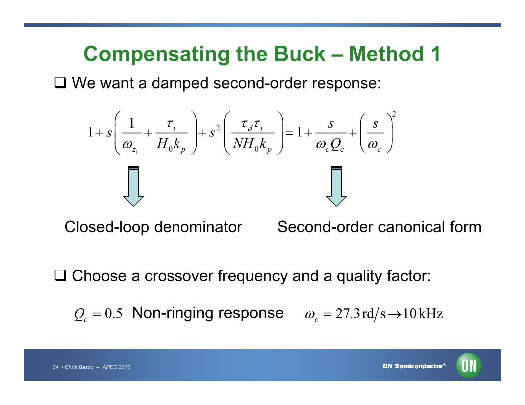
Compensating the Buck – Method 1
We want a damped second-order response:
1
2
2
0 0
11 1i d i
z p p c c c
s ss s
H k NH k Q
34 • Chris Basso – APEC 2012
Closed-loop denominator Second-order canonical form
Choose a crossover frequency and a quality factor:
0.5cQ Non-ringing response 27.3rd s 10 kHzc

Compensating the Buck – Method 1
1 0
1 1i
z p c c
T
H k Q
20
1d i
p c
T T
NH k
21 0
1d id i
T TT T
N
0 0
1di
TT
N Q
Four unknowns, four equations:
2 2 2 2 2 2 4 2 3 2 20 0 0 0 0 0 02
1.116 msc z c z c c c c z c c z c z cQ Q Q Q Q Q Q Q Q
T
35 • Chris Basso – APEC 2012
1 1 1 1 1
1 1 1
0 0 0 0 0 0 0
20 0 0
21.116 ms
c z c z c c c c z c c z c z c
d
c c c z c c z c c z
Q Q Q Q Q Q Q Q QT
Q Q Q Q
1 1 1 1 1
1 1 1
2 2 2 2 2 2 4 2 3 2 20 0 0 0 0 0 0
20 0 0
272.4
c z c z c c c c z c c z c z c
c z c c z c c z
Q Q Q Q Q Q Q Q QN
Q Q Q Q
1 1
1
20 0
20 0 0
14.6μsc c z c c z
i
z c c c
Q Q QT
Q Q Q
1 1 1
1
20 0
2
0 0 0
0.178c z c c z c c z
p
z c c
Q Q Q Qk
H Q Q

Compensating the Buck – Method 1
We can now compute our transfer functions in Mathcad®
20
0
20
40
60
100
0
100
20 log G1 i 2 f( ) 10 arg G1 i 2 f( ) 180
G s G s
Compensatorresponse G(s)
36 • Chris Basso – APEC 2012
10 100 1 103
1 104
1 105
20
f
10 100 1 103
1 104
1 105
40
20
0
20
40
60
100
0
100
20 log TOL i 2 f( ) 10 arg TOL i 2 f( ) 180
f
10 kHzcrossover
m = 80°
OLT s
OLT s
response G(s)
Open-loop gainresponse TOL(s)

Compensating the Buck – Method 1
The closed-loop system is perfectly compensated
20
10
0
0
100
20 log T1 i 2 f( ) 10 arg T1 i 2 f( ) 180
11.8 kHz-3 dB
CLT s
T s
37 • Chris Basso – APEC 2012
10 100 1 103
1 104
1 105
30
20
100
f
1
OL
CL
OL
T sT s
T s
CLT s

Compensating the Buck – Method 1
We can test the compensation with SPICE
Vout2
16
Cout
220u
Resr
70m
2 12
L1
75uvout
3
R6
100m
GA
IN
5
XPWM
GAIN
d
a c
PWM switch VM p
X7
PWMVM
L = 75u
Fs = 100k
parameters
fc=10kGfc=-20Vin=10Vpeak=2
G=10^(-Gfc/20)pi=3.14159
fz1=1.2kfz2=1.2kfp1=10kfp2=50k
Rload
2.5
Vin
Vin
AC = 0
X3
SUM2
K1 = 1
vout
910
C6
0.1u
R9
Td/0.1u
IntFilt
DeriveFilt
R11x
R10
Ti/0.1u
X5
AMPSIMP
5.00V
5.00V
5.10V 5.10V
511mV
10.0V
-1.27mV1.15V
0V 0V
38 • Chris Basso – APEC 2012
GA
IN
4
GAIN
K = 1/VpeakWz1=2*pi*fz1Wz2=2*pi*fz2Wp1=2*pi*fp1
i=(1+fc^2/fp1^2)*(1+fc^2/fp2^2)j=(1+fz1^2/fc^2)*(1+fc^2/fz2^2)Wpi=sqrt(i/j)*G*fz1*2*pi
e=(Wp1-Wz1)*(Wp1-Wz2)f=Wp1*Wz1+Wp1*Wz2-Wz1*Wz2
Td=e/(f*Wp1)N=((Wp1^2)/f)-1Ti=((Wz1+Wz2)/(Wz1*Wz2))-(1/Wp1)kpf=(Wpi/Wz1)-(Wpi/Wp1)+(Wpi/Wz2)
Tdd=1.116mTii=14.6ukpff=0.178NN=72.4
6
LoL
1kH
22
7
CoL
1kF
V1
AC = 1
TR13
100m
K
S+A 8
X6
POLE
FP = fp2
K = -1 SUM2
K1
K220
23
K1 = 1
K2 = -1
Vref
5
-
+
11 13
Td/0.1u
C7
0.1uF
K
S+A17
X1
POLE
FP = (N/Td)/(2*pi)
15
10k
18
R12
10k/kpfSUM3
K1
K2
K314
X4
SUM3
K1 = 1
K2 = 1
K3 = 1
X8
AMPSIMP
X9
AMPSIMP
25
X10
AMPSIMP
R8
10k
R11
10k
Vdirect
VPIDFiltered
1.02V
-1.02V
5.00V
-1.27mV
0V 0V
0V
1.12mV
1.15V1.26mV
-1.39uV
1.02V

Compensating the Buck – Method 1
We can test the compensation with SPICE
30.0
60.0
90.0
180 OLT s
OLT s
m = 80°
° dB
39 • Chris Basso – APEC 2012
10 100 1k 10k 100k
-60.0
-30.0
0
-180
-90.0
0
10-kHzcrossover
Perfect compensation dude!
Compensating the Buck – Method 1
5.00
5.04
5.08 2
10.128
21
20ln
45
1 2 3.9Q
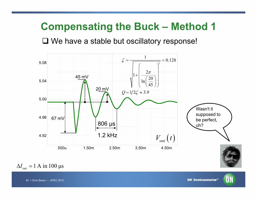
We have a stable but oscillatory response!
45 mV
20 mV
40 • Chris Basso – APEC 2012
500u 1.50m 2.50m 3.50m 4.50m
4.92
4.96
5.00
outV t
806 µs
1.2 kHz
67 mV
1 A in 100 μsoutI
Wasn't it supposed to be perfect, uh?

Compensating the Buck – Method 1
Bode or Nyquist do not predict the oscillatory response
2.00
4.00
1, 0j1/GM
m
OLT s
41 • Chris Basso – APEC 2012
-4.00 -2.00 0 2.00 4.00
-4.00
-2.00
0
1/GM
m
e
c

Compensating the Buck – Method 1
We compensated the Vout to Vref path only!
H(s)+
(s)
G(s)
outV sPWMG d(s)
T s
out outI s Z s
inin VV s G s
+
+
- refV s
42 • Chris Basso – APEC 2012
G(s)
10 100 103 104 10530
20
10
0
100
0
100
refV t
CLT s
CLT s
outV t
?

Compensating the Buck – Method 1
The output response is as expected
5.15
5.25
5.35
43 • Chris Basso – APEC 2012
300u 900u 1.50m 2.10m 2.70m
4.95
5.05
5.15
outV t
Where is the issue coming from then?
Course Agenda
Introduction to Control Systems
Shaping the Error Signal
How to Implement the PID Block?
The PID at Work with a Buck Converter
Considering the Output Impedance
44 • Chris Basso – APEC 2012
Considering the Output Impedance
Classical Poles/Zeros Placement
Shaping the Output Impedance
Quality Factor and Phase Margin
What is Delay Margin?
Gain Margin is not Enough

Compensating the Buck – Method 1
In reality, Vref is fixed: "we have a regulator, stupid!"
H(s)+
G(s)
,out out OLI s Z s
+
-
outV s refV s
45 • Chris Basso – APEC 2012
I think he's right…
Because the system is linear, superposition applies
1
1OL
out ref
OL
T sV s V s
T s
2 ,out out out OL out OLV s I s Z s V s T s
,
1 21 1
out OLOLout out out ref out
OL OL
Z sT sV s V s V s V s I s
T s T s
During the load step, : Zout fixes the response!
,out CLZ
ˆ 0refv
Compensating the Buck – Method 1
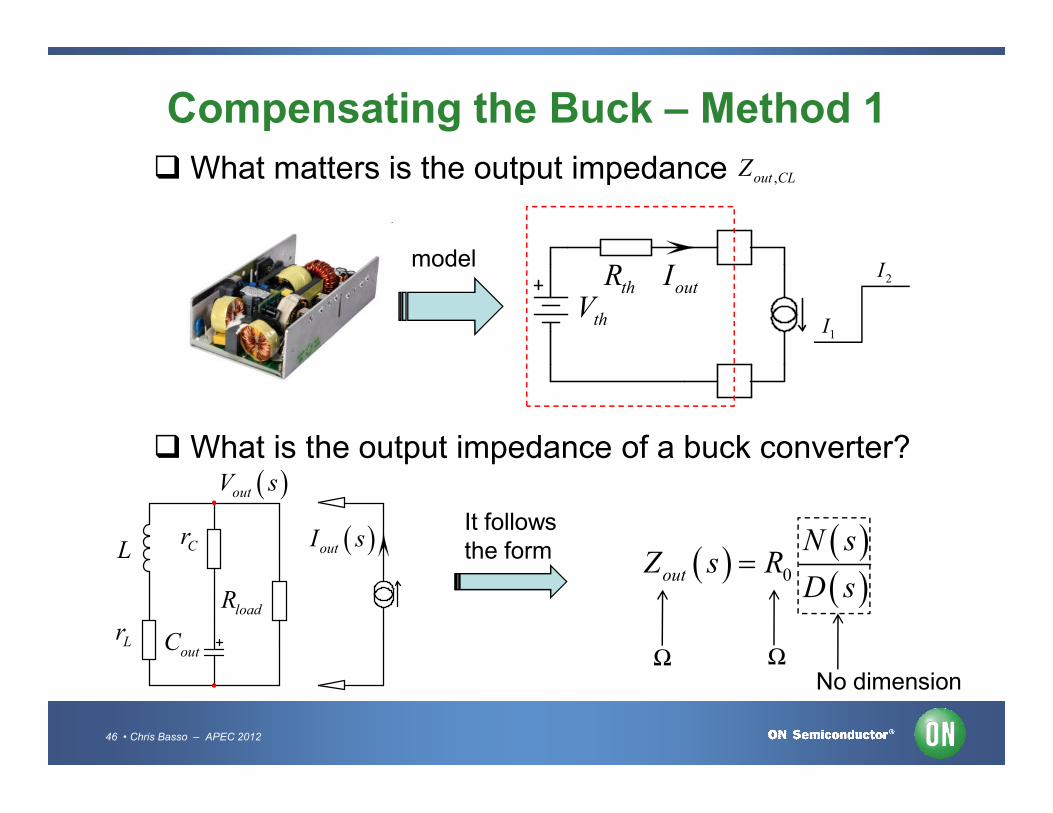
What matters is the output impedance
thVthR
,out CLZ
outI
1I
2Imodel
46 • Chris Basso – APEC 2012
What is the output impedance of a buck converter?
L
Lr
Cr
outC
loadR
outV s
outI s
0out
N sZ s R
D s
Ω ΩNo dimension
It follows the form
Compensating the Buck – Method 1
0 ||L loadR r R
outout
out
V sZ s
I s
The output impedance is a transfer function
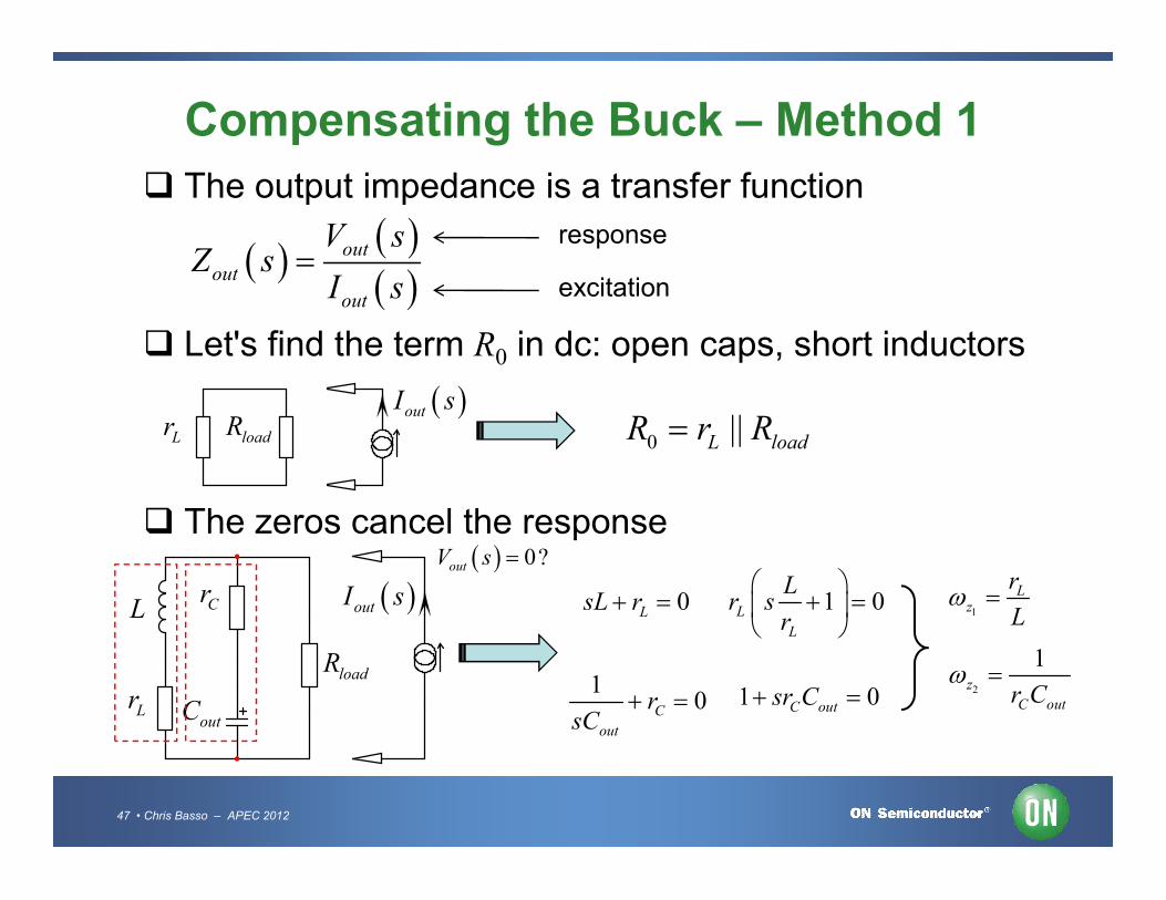
response
excitation
Let's find the term R0 in dc: open caps, short inductors
Lr loadR outI s
47 • Chris Basso – APEC 2012
0 L load
0LsL r
10C
out
rsC
1 0L
L
Lr s
r
1 0C outsr C
The zeros cancel the response
L
Lr
Cr
outC
loadR
outI s
2
1z
C outr C
1
Lz
r
L
0?outV s

Compensating the Buck – Method 1
The denominator is solely dependent on the structure
It is independent from the excitation: set it to zero!
There are two storage elements: this is a 2nd–order network
2
21 21 1
s sD s a s a s
48 • Chris Basso – APEC 2012
1 2
0 0
1 1D s a s a sQ
D must be dimensionless thus:
The two possible terms for a1 are
The two possible terms for a2 are
1
1a Hz
2
2a Hz
1 2
1 2' or
LRC
R
1 2'

Compensating the Buck – Method 1
For a1 look at the resistance R driving L and C
Look at the driving impedance at L while C is in its dc state Look at the driving impedance at C while L is in its dc state
49 • Chris Basso – APEC 2012
Lr Cr
loadR
L loadR r R
Lr Cr
loadR
||L load CR r R r
... ||L load C
L load
Ls C r R r
r R
?R ?R
1 2

Compensating the Buck – Method 1
how 1 (involving L) combines with '2 (involving C)? how 2 (involving C) combines with '1 (involving L)?
Look at the driving impedance at C while L is in its HF state Look at the driving impedance at L while C is in its HF state
a2
50 • Chris Basso – APEC 2012
Lr
?R
Lr Cr
loadR
2' c loadC r R
1
L load
L
r R
If we chose ?R
Cr
loadR
1'||L load C
L
r R r
2 ||L load CC r R r
If we chose
Same result
1 2 1 2' '

Compensating the Buck – Method 1
We have our denominator!
21 || C loadL load C
L load L load
r RLD s s C r R r s LC
r R r R
The complete transfer function is now:
51 • Chris Basso – APEC 2012
2
1 1
||
1 ||
C out
Lout L load
C loadL load C
L load L load
Ls sr C
rZ s r R
r RLs C r R r s LC
r R r R
See "Fast Analytical Techniques" from Vatché Vorpérian, Cambridge Press

Compensating the Buck – Method 1
It can be put under the following form:
1 2
0 2
0 0
1 1
1
z z
out
s sZ s R
s s
Q
Where we can identify the terms:
52 • Chris Basso – APEC 2012
Where we can identify the terms:
0 ||L loadR r R1
Lz
r
L
2
1z
C outr C
0
1 L load
C loadout
r R
r RLC
0out C load
out L C L load C load
LC r RQ
L C r r r R r R

Compensating the Buck – Method 1
If we now plot the output impedance, we see peaking For an non-oscillatory response, the peaking must be damped!
-7.00
3.00
0f
,maxoutZ
dBΩ
Z
53 • Chris Basso – APEC 2012
10 100 1k 10k 100k
-37.0
-27.0
-17.0
Cr
It's not, this is where the problem comes from
,out OLZ
,
1
out OL
OL
Z
T s
Compensating the Buck – Method 1
20
0
20
40
60
100
0
100
20 log G1 i 2 f( ) 10 arg G1 i 2 f( ) 180
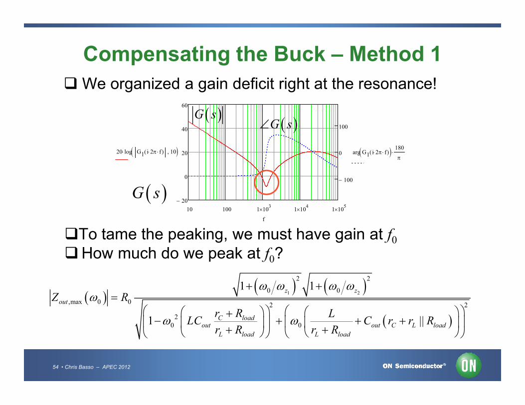
We organized a gain deficit right at the resonance!
G s
G s G s
54 • Chris Basso – APEC 2012
10 100 1 103
1 104
1 105
20
f
To tame the peaking, we must have gain at f0
How much do we peak at f0?
1 2
2 2
0 0
,max 0 0 2 2
20 0
1 1
1 ||
z z
out
C loadout out C L load
L load L load
Z R
r R LLC C r r R
r R r R

Compensating the Buck – Method 1
We can impose a magnitude to stay below rC
evaluate the needed gain to fulfill this goal:
,max 0
01
out
C
OL
Z fr
T f
,max 0
0
out
C
OL
Z fr
T f
,max 0
0
out
OL
C
Z fT f
r
Closed-loop output impedance
55 • Chris Basso – APEC 2012
Applying the numerical values of the buck:
0
1.1216or 24dB
70OLT f
m
Is this enough to obtain a ringing-free response?
output impedance

Compensating the Buck – Method 1
No, ringing is reduced but not eliminated
-50.0
-30.0
-10.0
5.00
5.04
5.08
dBΩ V
56 • Chris Basso – APEC 2012
The peaking in the output impedance is still there! The notched zeros are the cause for the gain dip at f0
We must find a different compensation method
10 100 1k 10k 100k
-90.0
-70.0
500u 1.50m 2.50m 3.50m 4.50m
4.92
4.96
Less than 0.4%
,
1
out OL
OL
Z
T sIncreasedOL gain outV t

Another (Bad) Example
Can we crossover at 10 Hz according to this plot?
90.0
180
20.0
40.0 10 Hz 14dBH dB °
57 • Chris Basso – APEC 2012
We have no phase lag at 10 Hz, a type 1 could do?10 100 1k 10k 100k
-180
-90.0
0
-40.0
-20.0
0
1
arg 10 Hz 0H

Rolling-off the BW at Low Frequencies
SPICE gives us the open-loop gain snapshot
vout
16
C51m
R101m
11
Vin10
3
L1100u vout
7
rLf10m
8 vout
d
a c
PWM switch VM p
X3PWMVML = 100uFs = 100k
parameters
Vout=5VRupper=10kfc=10Gfc=14
G=10^(-Gfc/20)pi=3.14159
C1=1/(2*pi*fc*G*Rupper)fp0=1/(2*pi*C1*Rupper)
R111
Vcp(t)
58 • Chris Basso – APEC 2012
5
Rupper10k
Rlower10k
6
X2AMPSIMP
V22.5
GA
IN
2
X1GAINK = 0.5
Vin
Verr
C1C1
LoL1kH
9
CoL1kF
VstimAC = 1
-6 dBPWM gain

The Open-Loop Gain Looks Good…
The type 1 confirms our 0-dB crossover frequency
90.0
180
20.0
40.0
dB ° T s
argT s
90m
59 • Chris Basso – APEC 2012
100m 1 10 101 1k 10k
-180
-90.0
0
-40.0
-20.0
0
m
10Hzcf
GM 24dB

As Expected: It is Ringing!
The load step reveals a ringing ac output
5.20
5.60
4748
V
outV t 01 f
2 AoutI
60 • Chris Basso – APEC 2012
Munch
Vcp(t) is first order5.50m 16.5m 27.5m 38.5m 49.5m
4.00
4.40
4.80
4748
cpV t

Good dc Coupling, Weak ac Coupling
H1 is stable per Bode analysis, but H2 is out of the loop…
Vout(s)
T(s)
Vin H1(s) H2(s)
61 • Chris Basso – APEC 2012
“Fast Analytical Techniques for Electrical and Electronic Circuits”, V. Vorpérian, Cambridge Press, 2002
The dc is fed back via the loop but not the ac… Oscillations are NOT due to the loop!
G(s)
dcf < fc
acf >> fc
d(s)
Loose couplingin ac, no signaltransmission >> fc…
T(s)

Again, an Undamped RLC Network…
No gain at resonance: the RLC network runs open loop
-20.0
0
20.0
dBΩ
output filter f0
Gain action
62 • Chris Basso – APEC 2012
The system cannot reduce the Q at the resonant frequency
Zout,OL
Zout,CL Properly compensated, fc = 4 kHz
Zout,CL
1 10 100 1k 10k 100k 1Meg
-60.0
-40.0
-20.0Gain action

Course Agenda
Introduction to Control Systems
Shaping the Error Signal
How to Implement the PID Block?
The PID at Work with a Buck Converter
Considering the Output Impedance
63 • Chris Basso – APEC 2012
Considering the Output Impedance
Classical Poles/Zeros Placement
Shaping the Output Impedance
Quality Factor and Phase Margin
What is Delay Margin?
Gain Margin is not Enough

Compensating the Buck – Method 2
In this method, we will focus on two parameters: crossover frequency fc
phase margin m
First, look at the ac response of the power stage:
resonance
dB °
18040.0
H s
64 • Chris Basso – APEC 2012
resonance
10 100 1k 10k 100k
-180
-90.0
0
90.0
-40.0
-20.0
0
20.0 H s
H s
ESR zero
-20 dB-132 °

Compensating the Buck – Method 2
The peaking in H brings a severe phase lag at f0
stay away from f0 , pick fc at least 10 times above (10 kHz) extract the phase/magnitude of H at 10 kHz:
10 kHz 20dBH 10 kHz 132H
The compensator G must shape the loop gain TOL by
65 • Chris Basso – APEC 2012
providing a high dc gain for precision: place an origin pole reducing the phase lag at 10 kHz to provide a m of 70°
What compensation type do we need?

Compensating the Buck – Method 2
The origin pole brings a permanent phase lag of 90° added to the op amp inversion of -180°, we have -270° total phase (op amp and H) must be -360 + 70° = -290° the needed phase boost at fc is thus:
90 70 132 90 112m cboost H f
G s G s
66 • Chris Basso – APEC 2012
10 100 1k 10k 100k
G s
G s
270
boost
1 2 5 10 20 50 100 200 500 1k
270G s
G s
10 100 1k 10k 100k
G s
G s
270
boost
Type 1 – no boost Type 2 – up to 90° Type 3 – up to 180°

Compensating the Buck – Method 2 type 3: an origin pole, a double zero and 2 poles
this is our PID compensator!
1
1 2 2
1
1 2 1 2
1 1 1 1
1 1 1 1
z
z z zpo
z
po p p p p
s s s
sG s
s s s s s
67 • Chris Basso – APEC 2012
1 2 1 2po p p p p
The magnitude is derived as:
1
2
1
1 2
22
2 2
1 1
1 1
z
zpo
z
p p
f f
f ffG f
ff f
f f
The argument is found to be:
arg arg argG f N D
1 2
arg arctan arctanp p
f fD
f f
1
2
arg arctan arctanz
z
f fN
f f

Compensating the Buck – Method 2
Place the double zero at f0 ,the second pole at Fsw/2
The 0-dB crossover pole is adjusted to provide +20 dB at fc
The first pole is adjusted to provide the right m
68 • Chris Basso – APEC 2012
1
2 1 2
arg arctan arctan arctan arctanz c c c
c
c z p p
f f f fG f
f f f f
1
1
2 2
1 1 1
10.8kHz
tan arg tan tan tan
cp
zc c
p c z
ff
ff fG
f f f

Compensating the Buck – Method 2
The 0-dB crossover pole is adjusted to give 20 dB at 10 kHz
1 2
1
1
2
2 2
22
1 1
2 kHz
1 1
c c
p p
po c z
z c
c z
f f
f ff G f f
f f
f f
69 • Chris Basso – APEC 2012
1.2 kHz
10.8 kHz
2 kHz
0 dB
|G(s)|
20 dB
doublezero (+2)
-1
-1+1
0
50 kHz
2c zf f
The final configuration is as follows:
1.2 kHz 1.2 kHz 1.2 kHz 37dBOLT G H
It should be ok to damp Zout

Compensating the Buck – Method 2
Enter the PID coefficients from the poles/zeros positions
55.5d u 250i u 3.76N 3.1pk
90.0
180
30
60
-30.0
-10.0
OLT s
dB °
Z
dB
70 • Chris Basso – APEC 2012
10 100 1k 10k 100k
-180
-90.0
0
90.0
-60
-30
0
30
10 100 1k 10k 100k
-90.0
-70.0
-50.0
-30.0
,
1
out OL
OL
Z
T s
OLT s
More than 30 dB at f0 and absolutely no peaking in Zout
,out CLZ-21 dBm = 70°

Compensating the Buck – Method 2
The transient response with a 0.1-A load step is excellent
4.998
5.000 outV t
71 • Chris Basso – APEC 2012
683u 906u 1.13m 1.35m 1.58m
4.992
4.994
4.996
, 10 21dB 84mΩout CLZ k
8 mV

Course Agenda
Introduction to Control Systems
Shaping the Error Signal
How to Implement the PID Block?
The PID at Work with a Buck Converter
Considering the Output Impedance
72 • Chris Basso – APEC 2012
Considering the Output Impedance
Classical Poles/Zeros Placement
Shaping the Output Impedance
Quality Factor and Phase Margin
What is Delay Margin?
Gain Margin is not Enough

Compensating the Buck – Method 3 The capacitor stray elements affect the transient response
Cr
ESR zoom80.0u 240u 400u 560u 720u
4.976
4.982
4.988
4.994
5.000
4.990
4.994
4.998
outV t
outV tCSl
Depends onCout fc m
73 • Chris Basso – APEC 2012
C
Cl
ESL
94.7u 102u 109u 117u 124u
4.982
4.986
4.990
94.7u 102u 109u 117u 124u
300m
500m
700m
900m
1.10
outI t
outI
t
C outr ICSl
outIS
t
R. Redl et al."Optimizing the Load Transient Response of the Buck Converter", APEC 1998

Compensating the Buck – Method 3
During a step load, the converter fights the current change
5.000
max min
2
V V
5.000
maxVmax minV V
74 • Chris Basso – APEC 2012
936u 1.16m 1.39m 1.61m 1.84m
outV t
500u 1.50m 2.50m 3.50m 4.50m
minV outV t
Traditional compensation:
inductive output impedance
Adaptive Voltage Positioning
resistive output impedance
Limited excursion Full-span excursion
Compensating the Buck – Method 3
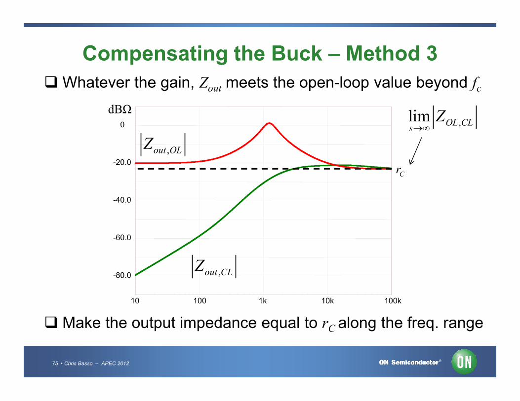
Whatever the gain, Zout meets the open-loop value beyond fc
Cr
dBΩ,lim OL CL
sZ
-40.0
-20.0
0
,out OLZ
75 • Chris Basso – APEC 2012
10 100 1k 10k 100k
-80.0
-60.0
-40.0
Make the output impedance equal to rC along the freq. range
,out CLZ

Compensating the Buck – Method 3
How to force the output impedance to be resistive?
1 2
1
,
, 0 2
0 00 2
1 11
1 111
z zout OL
out CL
z
s s
ZZ R
sT s s s
Q H G s
76 • Chris Basso – APEC 2012
0 00 2
0 0
1
1
Q H G ss s
Q
Extract G(s)to have:
,out CL CZ r
Compensating the Buck – Method 3
2
2
0
0 0
0
0
1 1
1
z
C
z
s s sRQ
G sr G s
G
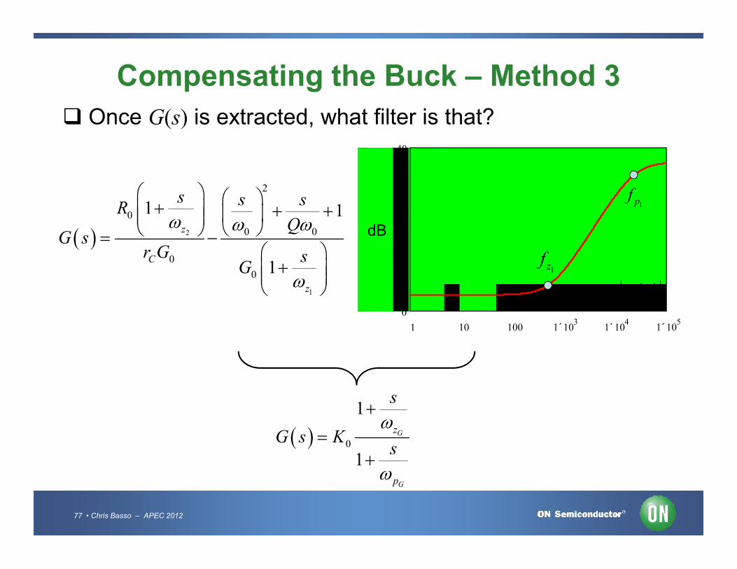
Once G(s) is extracted, what filter is that?
10
20
30
40
dB
G s
1pf
1zf
77 • Chris Basso – APEC 2012
1z
0
1
1
G
G
z
p
s
G s Ks
1 10 100 1 103
´ 1 104
´ 1 105
´
0
G s

Compensating the Buck – Method 3
Some parameter identification is now needed:
0
0
1.8L C
C
r rK
H r
1 2
20
47.7CL
z z
rra p
1 2 0
1 174.2C
L
z z
rb r u
Q
0.27L Cc r r 2 4
580 Hz4Gz
b b acf
a
124 kHz
Gp zf f
40
78 • Chris Basso – APEC 2012
YAO et al. ,"Design Considerations for VRM Transient Response Based on the Output Impedance", IEEE Proceedings, 2003
1 10 100 1 103
´ 1 104
´ 1 105
´
0
10
20
30
dB
G s
approximated

Compensating the Buck – Method 3
The following op amp architecture will do the job
1R2R 3R
1C
outV s
1
1
c
out
v s R
V s Z
1Z
2 3
11
1
1
R RsC
Z
79 • Chris Basso – APEC 2012
cv s
1
2 3
1
1R R
sC
1 2 32
1 3 1
1
1
sC R RRG s
R sR C
20
1
RK
R
1
1 2 3
1z
C R R
1
3 1
1p
R C
Compensating the Buck – Method 3
Vout2
16
Cout220u
Resr30m
2 12
L175u vout
3
R60.3
5
d
a c
PWM switch VM p
X7PWMVML = 75uFs = 100k
parameters
Vin=10Vpeak=2
pi=3.14159
fz1=580fp1=24k
Wz1=2*pi*fz1
Vin
Rload2.5
VinVinAC = 0
vout
5.00V
5.00V
5.30V 5.30V
531mV
10.0V
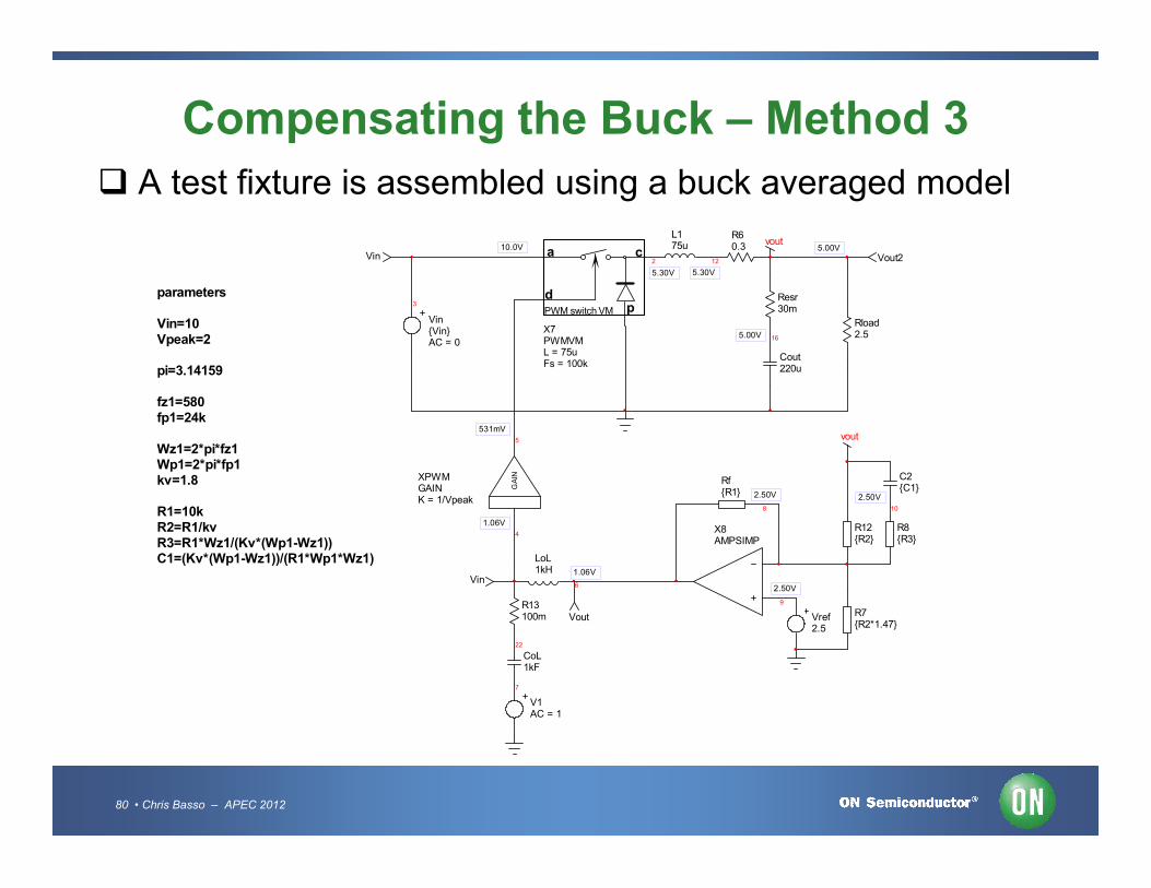
A test fixture is assembled using a buck averaged model
80 • Chris Basso – APEC 2012
GA
IN
4
5
XPWMGAINK = 1/Vpeak
Wz1=2*pi*fz1Wp1=2*pi*fp1kv=1.8
R1=10kR2=R1/kvR3=R1*Wz1/(Kv*(Wp1-Wz1))C1=(Kv*(Wp1-Wz1))/(R1*Wp1*Wz1)
6
LoL1kH
Vout
Vin
8
RfR1
9
X8AMPSIMP
Vref2.5
R7R2*1.47
R12R2
10
R8R3
C2C1
22
7
CoL1kF
V1AC = 1
R13100m
1.06V
2.50V
2.50V
2.50V
1.06V
Compensating the Buck – Method 3
-180
-90
0
0
20
40
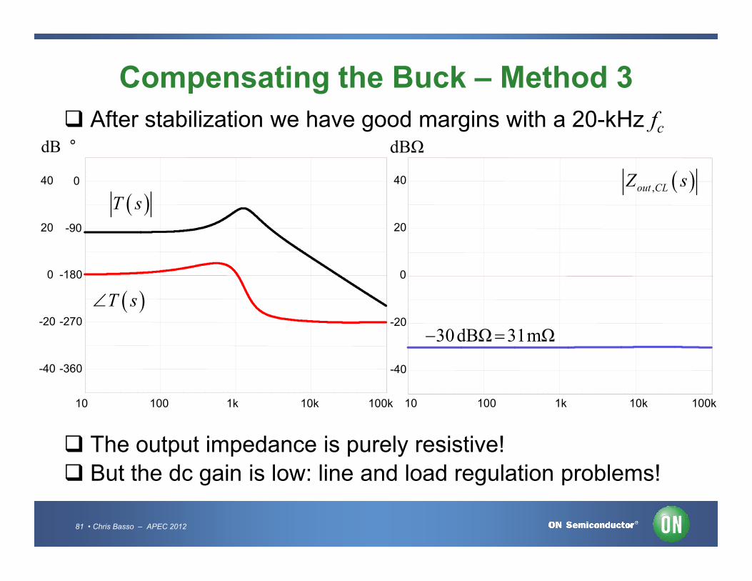
After stabilization we have good margins with a 20-kHz fc
T s
T s
0
20
40
dBΩdB °
,out CLZ s
81 • Chris Basso – APEC 2012
10 100 1k 10k 100k
-360
-270
-40
-20
T s
10 100 1k 10k 100k
-40
-20
The output impedance is purely resistive!
But the dc gain is low: line and load regulation problems!
30dBΩ 31mΩ

Compensating the Buck – Method 3
Also, the gain expression K0 can be a problem:
0
0
0L CL C
C
r rK r r
G r
4.995
5.005 30 mV
82 • Chris Basso – APEC 2012
500u 1.50m 2.50m 3.50m 4.50m
4.965
4.975
4.985
outV t1AoutI
VM, fixed frequency, is not the best for Zout resistive shaping

Compensating the Buck – Method 3
Going current-mode, fixed frequency is one way to go
vc
a c
PWM switch CM p
duty-cycle L Lr
Cr
C
loadRinV
outv s
83 • Chris Basso – APEC 2012
Use the PWM switch model in current-mode for Zout
outC
G s
cv s

Compensating the Buck – Method 3
The large-signal model combines two current-sources
vc
a c
p
duty-cycle
a c
cdI
aI cI
2c L
i
v I
R
2I1I
84 • Chris Basso – APEC 2012
PWM switch CM p
p
2iR
LI t offt
LIoutV L
2
1
2
swcout
i
D TvI V
R L
c
i
v
RcI

Compensating the Buck – Method 3
For ac study, we must obtain a small-signal model
2
11
,2 2
outsw
inswc cout c out out
i i
VT
VD TV VI V V V V
R L R L
Calculate the partial derivative coefficients to vout and vc
85 • Chris Basso – APEC 2012
2 2ˆ 2
ˆ ˆ ˆ12
c sw outc out out
c out i in
v T VI Iv v v
V V R L V
Update the schematic with this linear source
as R, L and C are also linear, Laplace applies
gm

Compensating the Buck – Method 3
We look at the output impedance closed-loop
L Lr
Cr
outv s
loadR gmc
out
v sv s
R outi s
2I
86 • Chris Basso – APEC 2012
G s
cv s
outC
out
iR
2gm 1
2sw out
in
T V
L V
Compensating the Buck – Method 3
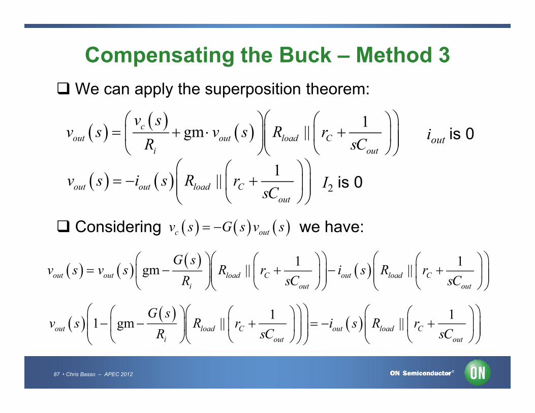
We can apply the superposition theorem:
1
gm ||c
out out load C
i out
v sv s v s R r
R sC
iout is 0
1
||out out load C
out
v s i s R rsC
I2 is 0
87 • Chris Basso – APEC 2012
Considering we have: c outv s G s v s
1 1
gm || ||out out load C out load C
i out out
G sv s v s R r i s R r
R sC sC
1 1
1 gm || ||out load C out load C
i out out
G sv s R r i s R r
R sC sC

Compensating the Buck – Method 3
The output impedance is thus:
,
1||
ˆ
ˆ 11 gm ||
load C
outout
out CL
out
load C
i out
R rsCv s
Z si s G s
R rR sC
Giving a small massage, we obtain:
88 • Chris Basso – APEC 2012
Giving a small massage, we obtain:
,
1
gm gm1
gm
load i C outout CL
i load i load i load i C load C i load Cout
i load i load
R R sr CZ s
R G s R R R R R R r G s R r R R rsC
R G s R R R
"There is a massage for you"

Compensating the Buck – Method 3
Factoring and re-arranging, we have:
1
1
,
1
1
z
out CL
p
sZ s R s
s
gmload i
i load i load
R RR s
R G s R R R
1
1z
C outr C
1
1
gm
gm
p
i load i C load C i load Cout
R R R r G s R r R R rC
R G s R R R
89 • Chris Basso – APEC 2012
gmout
i load i loadR G s R R R
Now make Zout,CL(s) = rC and extract G(s):
2 2gm1
gm gm
1
load C Cout
i load C load C load C load C
C load C out
R r rsC
R R r R r R r R rG s
r R sr C

Compensating the Buck – Method 3
The compensator brings a single pole/zero response
1
1
0
1
1
z
p
sG s G
s
0
gmi load C load C i
C load C
R R r R r RG
r R r
1
1p
out CC r
1 2 2 2
1 1
gm
gm
z
load C C Cout out
load C load C load
R r r rC C
R r R r R
Very high frequencycan be neglected
dB °
90 • Chris Basso – APEC 2012
0.6Ω
30 mΩ
220μF
i
C
out
R
r
C
10 100 103
104
105
106
10
0
10
20
30
100
0
100 G s
G s
dB °

Compensating the Buck – Method 3 Sub-harmonic oscillations at can cause peaking
Place a zero at as recommended by YAO and al.
2swF
swF
1RR R
1C
outV s
1
1
c
out
v s R
V s Z 1Z
2 3
1
1R R
sCZ
91 • Chris Basso – APEC 2012
YAO et al. ,"Design Considerations for VRM Transient Response Based on the Output Impedance", IEEE Proceedings, 2003
12R 3R
cv s
11
2 3
1
1
sCZ
R RsC
1 2 32
1 3 1
1
1
sC R RRG s
R sR C
20
1
RG
R
1
1 2 3
1z
C R R
1
3 1
1p
R C

Compensating the Buck – Method 3
Run the SPICE simulation with the CM PWM switch model
Vout2
16
Cout220u
Resr30m
2 12
L175u vout
3
R60.02
4
Vin
d
vc
a c
PWM switch CM p
duty-cycle
X3PWMCCMCML = 75uFs = 100kRi = 0.6Se = Se
VinVinAC = 0
R12.5
AC = 1I2
5.05V
5.05V
5.09V 5.09V
10.2V
1.42V
499mV
parameters
Vin=10.18se=20kFsw=100kpi=3.14159
pi=3.14159Ri=0.6
Slopecomp.
92 • Chris Basso – APEC 2012
6
RfxR1
R12R2
9
X8AMPSIMP
Vrefx2.5
R7R2
vout
10
R14R3
C2C12.50V
2.50V
2.50V
Ri=0.6Cout=220urC=30mwp=1/(rC*Cout)
Wz1=pi*FswWp1=1/(rC*Cout)G=Ri/rC
R1=10kR2=R1/GR3=R1*Wz1/(G*(Wp1-Wz1))C1=(G*(Wp1-Wz1))/(R1*Wp1*Wz1)
Automated calculations

Compensating the Buck – Method 3
-180
-90.0
0
90.0
180
-40.0m
-20.0m
0
20.0m
40.0m
The output impedance is resistive, the system is stable.
,out CLZ s
,out CLZ s
Ω °
93 • Chris Basso – APEC 2012
10 100 1k 10k 100k 1Meg
-180-40.0m
10 100 1k 10k 100k 1Meg
-40.0
-20.0
0
20.0
40.0
-180
-90.0
0
90.0
180 66m
40kHzcf
OLT s OLT s
Compensating the Buck – Method 3
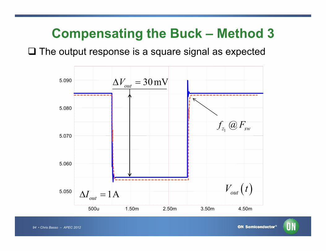
The output response is a square signal as expected
5.080
5.090 30 mVoutV
@z swf F
94 • Chris Basso – APEC 2012
500u 1.50m 2.50m 3.50m 4.50m
5.050
5.060
5.070
outV t1AoutI
1@z swf F

Course Agenda
Introduction to Control Systems
Shaping the Error Signal
How to Implement the PID Block?
The PID at Work with a Buck Converter
Considering the Output Impedance
95 • Chris Basso – APEC 2012
Considering the Output Impedance
Classical Poles/Zeros Placement
Shaping the Output Impedance
Quality Factor and Phase Margin
What is Delay Margin?
Gain Margin is not Enough
5.00
7.00
9.001 8.21 VpeakV
3 6.33 VpeakV
6.33 50.414
8.21 5k
5.00
7.00
9.001 8.21 VpeakV
3 6.33 VpeakV
6.33 50.414
8.21 5k
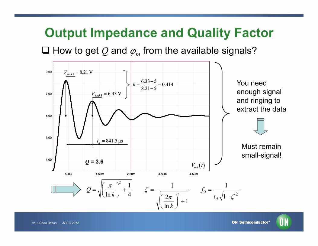
Output Impedance and Quality Factor
How to get Q and m from the available signals?
You need enough signal and ringing to extract the data
96 • Chris Basso – APEC 2012
500u 1.50m 2.50m 3.50m 4.50m
1.00
3.00
outV t
841.5 μsdt
500u 1.50m 2.50m 3.50m 4.50m
1.00
3.00
outV t
841.5 μsdt
21
ln 4Q
k
0
2
1
1d
ft
2
1
21
ln k
Q = 3.6
Must remain small-signal!
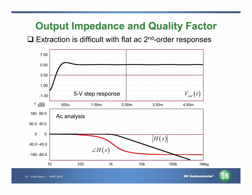
Output Impedance and Quality Factor Extraction is difficult with flat ac 2nd-order responses
-1.00
1.00
3.00
5.00
7.00
outV t5-V step response
97 • Chris Basso – APEC 2012
500u 1.50m 2.50m 3.50m 4.50m
-1.00
10 100 1k 10k 100k 1Meg
-80.0
-40.0
0
40.0
80.0
-180
-90.0
0
90.0
180
out
H s
H s
dB
Ac analysis

Output Impedance and Quality Factor
-20.0
-10.0
0
10.0
20.0 H sQ = 10
Q = 5
Q = 3
Q = 1Q = 0.6
dB
The phase drops at a different pace as Q changes
98 • Chris Basso – APEC 2012
10 100 1k 10k 100k 1Meg
-20.0
10 100 1k 10k 100k 1Meg
-170
-130
-90.0
-50.0
-10.0 H sQ = 10Q = 5
Q = 3
Q = 1
Q = 0.6
°

Output Impedance and Quality Factor Is there a link between Q and the phase rate of change?
g
d
d
[s]
2
1H s
s s
2
1
1
H j
j
Group delay
Let's apply the definition to a 2nd-order network:
s j
99 • Chris Basso – APEC 2012
0 0
1s s
Q
2
00
1 jQ
a b
2 2
2 22
200
1
1
H a b
Q
1 1
20
20
1tan tan
1
bH
a Q

Output Impedance and Quality Factor
We can apply g definition to the argument
1
20
2 220 00
2 4 2 2 2 2 4 2 20 0 0
1tan
1
2g
dQ
Q
d Q Q Q
100 • Chris Basso – APEC 2012
0 0 02d Q Q Q
0
2g
Q
0
At 0 the following formula links Q to the group delay
0
02
g
gQ f

Output Impedance and Quality Factor
Let's apply the theory to a classical case, the RLC filter
2
L1L
C1C
Vout
parameters
Vp=5f0=1.2kL=10uC=1/(4*3.14159^2*f0^2*L)w0=(L*C)^-0.5
3
V1AC = 1
R1R
Vin
out
101 • Chris Basso – APEC 2012
w0=(L*C)^-0.5Q=0.6R=L*w0/QR2=1/(Q*C*w0)Q1=(sqrt(L/C))/RDzeta=(R/2)*sqrt(C/L)Dzeta1=R/(2*L*w0)Q3=1/(2*Dzeta)per=1/(f0*sqrt(1-Dzeta^2))tp=1/(2*f0*sqrt(1-Dzeta^2))
plot the ac response
calculate the group delay
see if we can find Q

Output Impedance and Quality Factor
-170
-130
-90.0
-50.0
-10.0
01
0 1207 Hzf
outZ s
102 • Chris Basso – APEC 2012
10 100 1k 10k 100k 1Meg
20.0u
80.0u
140u
200u
260u
158 μsg
0 1207 158 3.14159 0.599gQ f u
Group delay

Output Impedance and Quality Factor
Knowing Q can also lead us to the phase margin m
40.0
80.0
90.0
180
m
OLT f OLT f
dB
Approximation of T(s)around fc
103 • Chris Basso – APEC 2012
0 2
1
1OLT s
s s
10 100 1k 10k 100k
-80.0
-40.0
0
-180
-90.0
0
-2
-1
cf
Open-loop ac analysis
0
2
0 dB

Output Impedance and Quality Factor
0 2
1
1OLT s
s s
2
0 2 0
1
1
1
OL
OL s s
T s
T s
If we consider the open-loop gain around fc only…
2 2
1 1
1 1s s s s
0cQ
0 2c
Closed-loop
Identify
Unity return
104 • Chris Basso – APEC 2012
20 2 0
1 1c c c
s s s s
Q 2
Closed-loopdata
Open-loopdata
We want to link Qc and the crossover frequency
0 2
1
1OLT s
s s
20 2cQ
22 2
1
1OL
c
T ss s
Q
Output Impedance and Quality Factor
42 1 4 1
2
c
c
Q
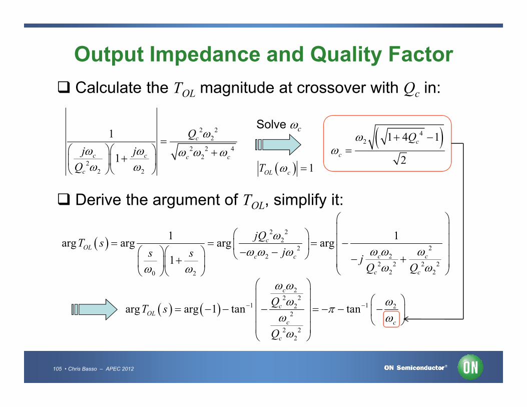
Calculate the TOL magnitude at crossover with Qc in:
2 22
2 2 42
22 2
1
1
c
c c c c
c
Q
j j
Q
Solve c
1OL cT
Derive the argument of TOL, simplify it:
105 • Chris Basso – APEC 2012
Derive the argument of TOL, simplify it:
2 2
222
222 2 2 2
2 20 2
1 1arg arg arg arg
1
cOL
c cc c
c c
jQT s
js sj
Q Q
22 2
1 12 22
2 22
arg arg 1 tan tan
c
cOL
c c
c
QT s
Q

Output Impedance and Quality Factor
If we substitute c by its definition, we have:
1 1
4 4
2 2arg tan tan
1 4 1 1 4 1OL
c c
T sQ Q
60.0180
T s OL c mT f
dB
106 • Chris Basso – APEC 2012
1 10 100 1k 10k 100k
-60.0
-30.0
0
30.0
-180
-90.0
0
90.0
OLT s
OLT sm
cf
OL cT f
OL c m
m OL cT f
1
4
2tan
1 4 1m
cQ

8
Output Impedance and Quality Factor
We can now extract the closed-loop quality coefficient:
24 1 tan cos
tan sin
m m
c
m m
Q
Qc10
2010m
20m
dB
10
2010m
20m
dB
Q
4
1
2
4 1 1cos
2
c
m
c
Q
Q
107 • Chris Basso – APEC 2012
0 20 40 60 80 1000
2
4
6Q m
m360
2
0.5
76°
m
20
10
0
10
90m
20m
10 100 1 kHz 10 kHz 100 kHz
30m
45m -3 dB
1
T s
T s20
10
0
10
90m
20m
10 100 1 kHz 10 kHz 100 kHz
30m
45m -3 dB
1
T s
T s
cQ
Closed-loop gain

Output Impedance and Quality Factor
The formula considers the vicinity of fc only: precision?
-60.0
0
60.0
120
-40.0
0
40.0
80.0
dB
OLT s
OLT s
cf
23m
4.92
5.00
5.08
5.16 128 mV
47 mV
Double zero
108 • Chris Basso – APEC 2012
1 10 100 1k 10k 100k
-120
-60.0
-80.0
-40.0cf
869u 1.15m 1.43m 1.70m 1.98m
4.84
4.92
outV t
2
13.1
47 4ln
128
cQ
4
1
2
4 1 1cos 18
2
c
m
c
Q
Q
Double zeroclose to fc
Step-load response
"Revisiting the Response of Closed Loop of PWM Converters ", S. Ben-Yaakov, IEEE Apec 2008

Output Impedance and Quality Factor We can ac sweep the output impedance also and check g
-80.0
-60.0
-40.0
-20.0
0
-20.0
20.0
60.0
100
140
dB
outZ s
outZ s
3.5 kHz
109 • Chris Basso – APEC 2012
1 10 100 1k 10k 100k
-240u
-120u
0
120u
240u
253 μsg Group delay
0 3.5 253 3.14159 2.8gQ f k u 20.4m
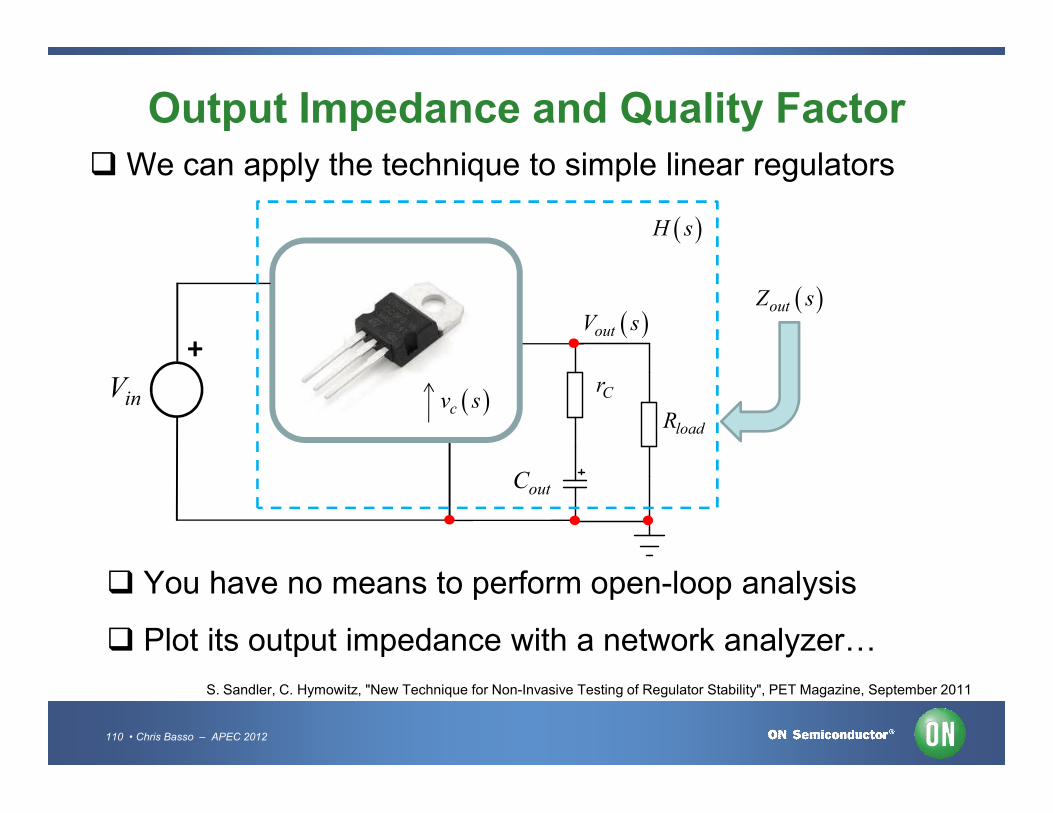
Output Impedance and Quality Factor We can apply the technique to simple linear regulators
+
inV Cr
outV s outZ s
H s
cv s
110 • Chris Basso – APEC 2012
in
outC
loadR
You have no means to perform open-loop analysis
Plot its output impedance with a network analyzer…
cv s
S. Sandler, C. Hymowitz, "New Technique for Non-Invasive Testing of Regulator Stability", PET Magazine, September 2011

Output Impedance and Quality Factor
Plot magnitude and phase of Zout and compute g
-80.0
-60.0
-40.0
-20.0
0
-40.0
0
40.0
80.0
120
500u
outZ s outZ s
dBΩ
111 • Chris Basso – APEC 2012
0 1 574.9 3.14159 1.8gQ f k u
4 4
1 1 1
2 2
4 1 1 4 1.8 1 1cos cos cos 857 31
2 2 1.8m
Qm
Q
10 100 1k 10k 100k
-300u
-100u
100u
300u
500u
574.9 μsg Group delay
Output Impedance and Quality Factor
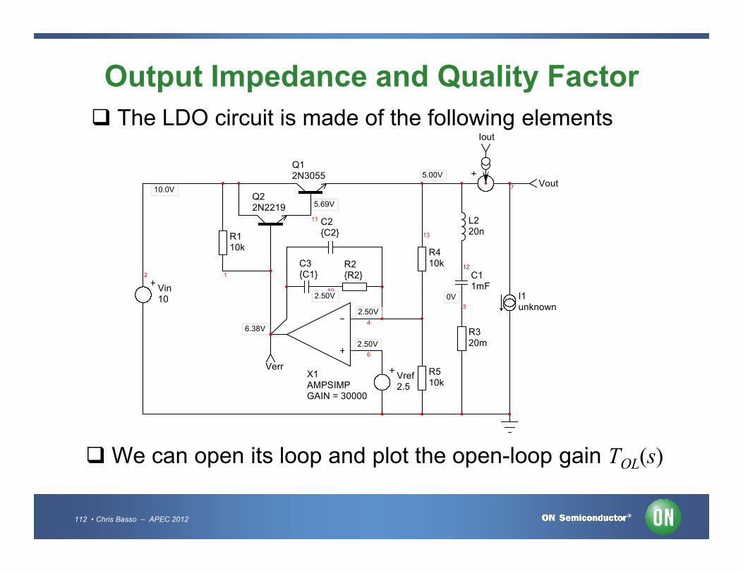
The LDO circuit is made of the following elements
12
Vin
12
C11mF
7 Vout
13
R410k
R110k
C3C1
C2C2
R2R2
11
Q12N3055
Q22N2219
L220n
Iout
10.0V
5.00V
5.69V
112 • Chris Basso – APEC 2012
Vin10
3
1mF
6
4
X1AMPSIMPGAIN = 30000
Vref2.5
R510k
R320m
Verr
10I1unknown
0V
2.50V
2.50V
6.38V
2.50V
We can open its loop and plot the open-loop gain TOL(s)

Output Impedance and Quality Factor
The open-loop plot confirms the experimental results
90.0
180
40.0
80.0
30m OLT s
113 • Chris Basso – APEC 2012
10 100 1k 10k 100k
-180
-90.0
0
-80.0
-40.0
0
1 kHzcf
OLT s
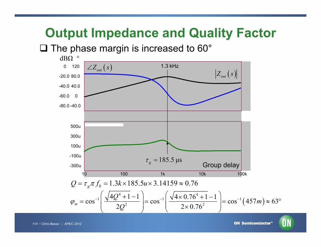
Output Impedance and Quality Factor The phase margin is increased to 60°
-40.0
0
40.0
80.0
120
-80.0
-60.0
-40.0
-20.0
0 outZ s outZ s
dBΩ °1.3 kHz
114 • Chris Basso – APEC 2012
0 1.3 185.5 3.14159 0.76gQ f k u
4 4
1 1 1
2 2
4 1 1 4 0.76 1 1cos cos cos 457 63
2 2 0.76m
Qm
Q
10 100 1k 10k 100k
-300u
-100u
100u
300u
500u
185.5 μsg Group delay

Course Agenda
Introduction to Control Systems
Shaping the Error Signal
How to Implement the PID Block?
The PID at Work with a Buck Converter
Considering the Output Impedance
115 • Chris Basso – APEC 2012
Considering the Output Impedance
Classical Poles/Zeros Placement
Shaping the Output Impedance
Quality Factor and Phase Margin
What is Delay Margin?
Gain Margin is not Enough

Considering a Delay in the Loop
Before a decision is actually executed, a delay occurs
The delay can be digital (computation time) or analogue
A typical delay is the duty-ratio conversion in a VM converter
+G
V t
5 V
ont
ontd +
G
V t
5 V
ont
ontd
116 • Chris Basso – APEC 2012
+
-
+
-
errV t
compensator
d t
pV
swT
0 V
rampV t
errV t
rampV t
swTsw
dT
+
-
+
-
errV t
compensator
d t
pV
swT
0 V
rampV t
errV t
rampV t
swTsw
dT
Prop. delay inthe 50 – 100 ns range

A Delay is a Time-Domain Shift
The output signal is the input signal that occured s before
t
u t
y t
delayadvance
t
u t
y t
delayadvance
y t u t
117 • Chris Basso – APEC 2012
t
t1 t2
Time delay
u t y t
t
t1 t2
Time delay
u t y t

Deriving the Delay
1
2
0 0
1
1
zs
s s
Q
errV s outV s d s1
peakV
cv s
H sThe plant
1
2
0 0
1
1
zs
s s
Q
errV s outV s d s1
peakV
cv s
H sThe plant
To account for the delay, we need its Laplace expression
118 • Chris Basso – APEC 2012
delay ?

Deriving the Delay
To account for the delay, we need its Laplace expression
y t u t
Let's start with a sinewave phasor expression
119 • Chris Basso – APEC 2012
j tu t Ae
y t
Time delay
j ty t Ae
a b a be e e j t j t j jy t Ae Ae e u t e
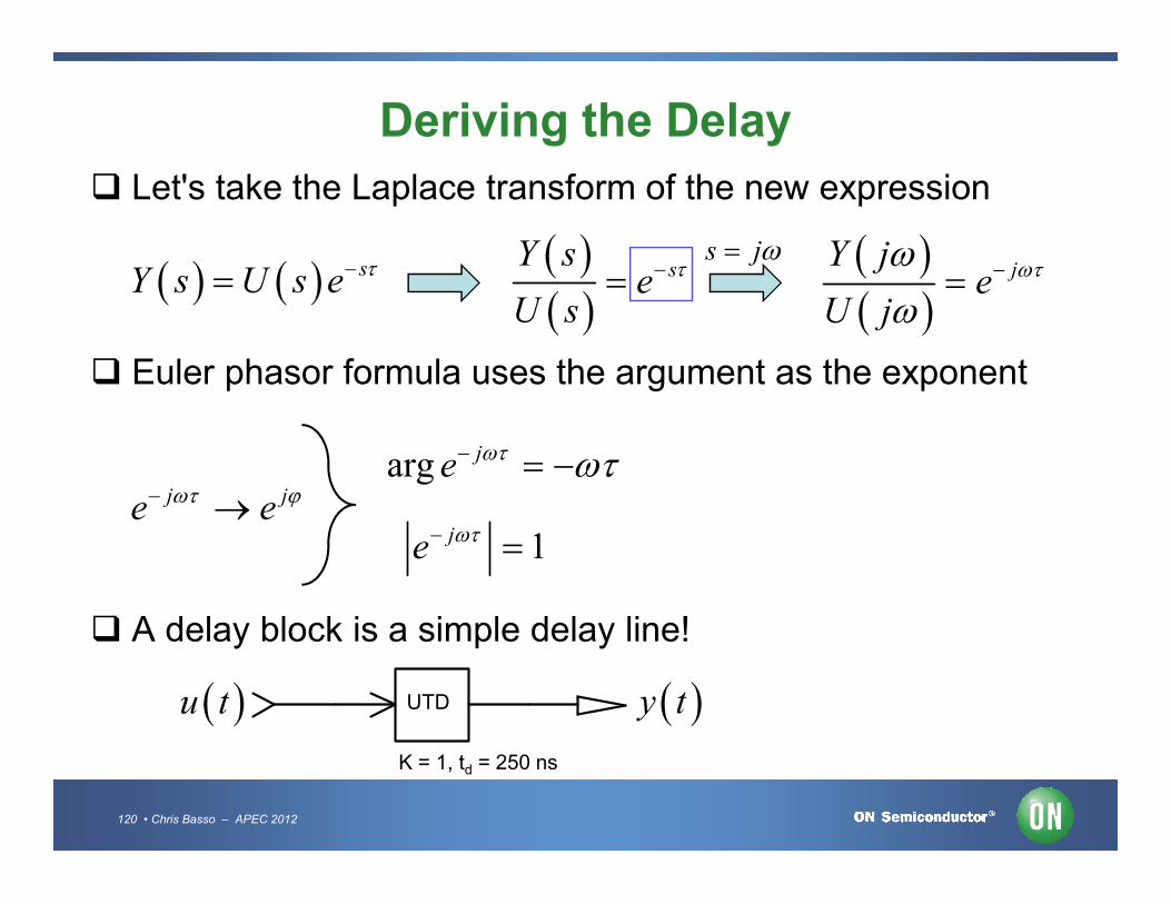
Deriving the Delay
Let's take the Laplace transform of the new expression
sY s U s e
sY s
eU s
Euler phasor formula uses the argument as the exponent
arg je
jY j
eU j
s j
120 • Chris Basso – APEC 2012
j je e arg je
1je
A delay block is a simple delay line!
UTD u t y t
K = 1, td = 250 ns

Building the Delay
A delay line can time-shift the input signal
1
2 Vout
3
parameters
tau=250nT1TD = Tau50 = Zo
Delay block
1
2 Vout
3
parameters
tau=250nT1TD = Tau50 = Zo
Delay block
121 • Chris Basso – APEC 2012
1
R150
E11
3
4
E21
VinAC = 1
1
R150
E11
3
4
E21
VinAC = 1
Best simulation practice is to buffer the input and the output
D. Adar, S. Ben-Yaakov, "Generic Average Modeling and Simulation of Discrete Controllers ", APEC Anaheim, 2001
Building the Delay
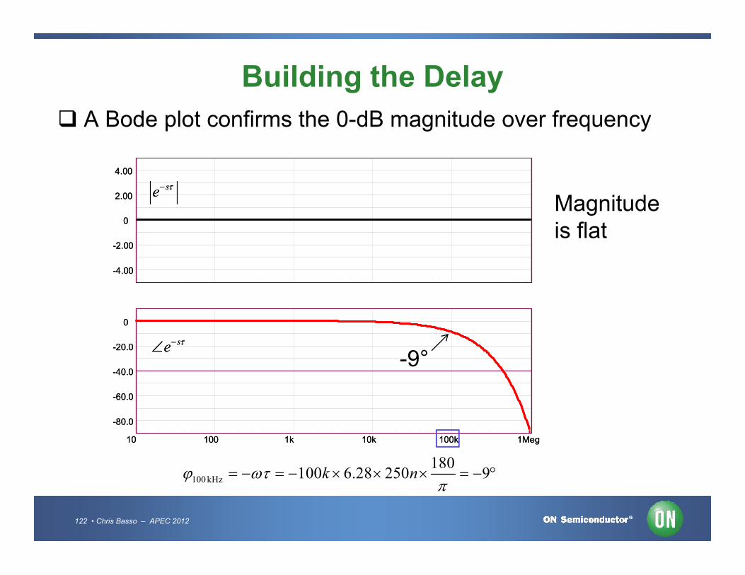
A Bode plot confirms the 0-dB magnitude over frequency
-4.00
-2.00
0
2.00
4.00
se
-4.00
-2.00
0
2.00
4.00
se
Magnitudeis flat
122 • Chris Basso – APEC 2012
10 100 1k 10k 100k 1Meg
-80.0
-60.0
-40.0
-20.0
0
se
10 100 1k 10k 100k 1Meg
-80.0
-60.0
-40.0
-20.0
0
se
100 kHz
180100 6.28 250 9k n
-9°

Adding the Delay in the Laplace Domain
We can now update our transmission chain with the delay
1
2
1
1
zs
s s
Q
errV s outV s d s1 st
peak
eV
cv s
H sThe plant
1
2
1
1
zs
s s
Q
errV s outV s d s1 st
peak
eV
cv s
H sThe plant
123 • Chris Basso – APEC 2012
0 0Q peak
0 0Q peak
1
2
0 0
1
1
sz
peak
seH s
V s s
Q

Adding the Delay in the Laplace Domain
How do you deal with the term in the transfer function?
You don't: replace it with a poles/zeros combination!
A pole will bring phase shift as frequency increases
ste
1
1 s 1arg tan
124 • Chris Basso – APEC 2012
But you still need to compensate the transmittance decrease
A zero will do but now, all is neutralized!
1
1
s
s
2
2
1
mag 1
1
1 1arg tan tan 0
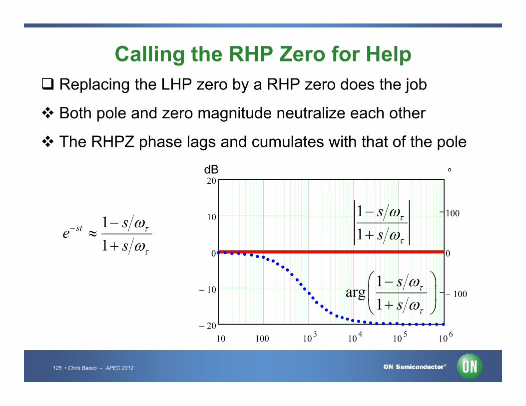
Calling the RHP Zero for Help
Replacing the LHP zero by a RHP zero does the job
Both pole and zero magnitude neutralize each other
The RHPZ phase lags and cumulates with that of the pole
20
1 s
dB °
125 • Chris Basso – APEC 2012
1
1st s
es
10 100 103
104
105
106
20
10
0
10
100
0
1001
1
s
s
1arg
1
s
s

Mapping the Delay to the Pole/Zero Position
Both arguments must be equal:
1arg arg
1s s
es
arg 1 arg 1s s
Replacing s by j:
126 • Chris Basso – APEC 2012
1 1 1tan tan 2 tan
Use the arctangent Taylor series equivalent:
31
5
ta ...3
n5
xxx
x
3 5
23 5
0

We Have the Padé Approximation
2
Solving for gives us…
Substituting in our first expression
12s
s
es
Henri Padé1863-1953
127 • Chris Basso – APEC 2012
12
es
This is the 1st-order Padé approximant of an exponential
12
12
x
x
ex
2nd-order 2
2
1 11
2 121 1
12 12
xx x
e
x x
http://en.wikipedia.org/wiki/Padé_approximant

Padé Approximant Frequency Response
dB °
0
2
40
20
0
1 2arg
1 2
s
s
se
dB °
0
2
40
20
0
1 2arg
1 2
s
s
se
When frequency increases, a phase deviation occurs
128 • Chris Basso – APEC 2012
10 100 1 10 3 1 10 4 1 10 5 1 10 6
2
0
80
60
se
1 2
1 2
s
s
10 100 1 10 3 1 10 4 1 10 5 1 10 6
2
0
80
60
se
1 2
1 2
s
s
Use higher order approximants to improve precision

How to Avoid the Delay Line?
A delay line adds computational burden in simulations
Is there any simpler circuit that could be used?
2 3
R11/(10n*Wtau)
C1K1
Vdelay1
parameters
tau=250nWtau=2/tau
129 • Chris Basso – APEC 2012
1
C110n SUM2
K2
5
X2SUM2K1 = 1K2 = 1
Vdelay1
E31k
6
E41
C210n
7
R31/(10n*Wtau)
V1AC = 1
11 1 1 1 1
1
11
out
RV s V s V s V s sR C
sC
RHPZ
1V s
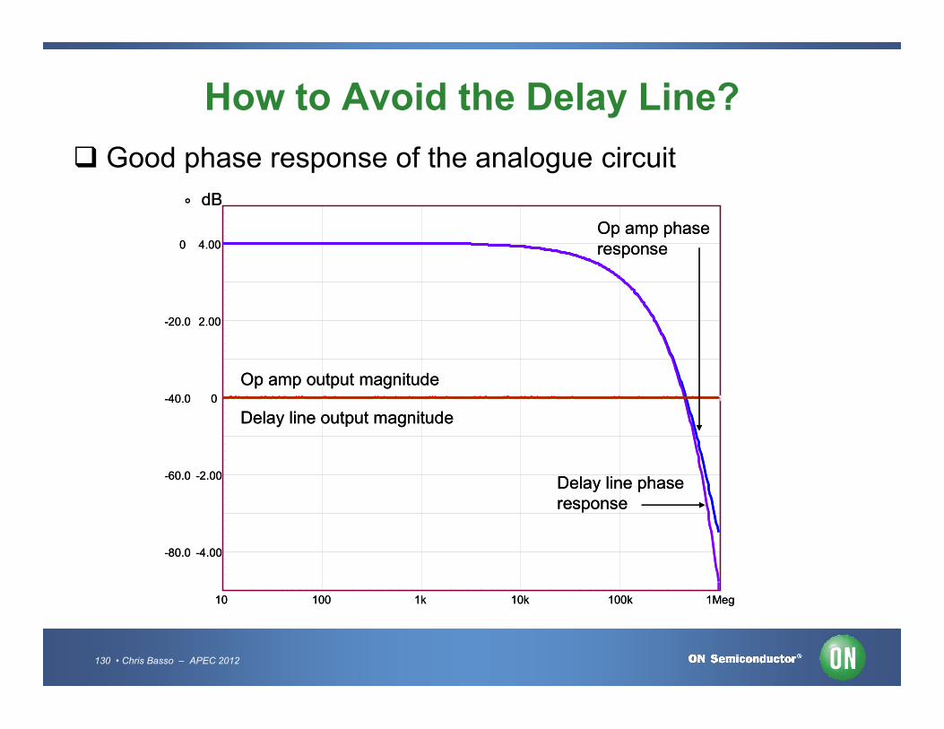
How to Avoid the Delay Line?
2.00
4.00
-20.0
0
dB°
Op amp phase response
2.00
4.00
-20.0
0
dB°
Op amp phase response
Good phase response of the analogue circuit
130 • Chris Basso – APEC 2012
10 100 1k 10k 100k 1Meg
-4.00
-2.00
0
-80.0
-60.0
-40.0 1112
Op amp output magnitude
Delay line output magnitude
Delay line phase response
10 100 1k 10k 100k 1Meg
-4.00
-2.00
0
-80.0
-60.0
-40.0 1112
Op amp output magnitude
Delay line output magnitude
Delay line phase response
Delay Margin versus Phase Margin
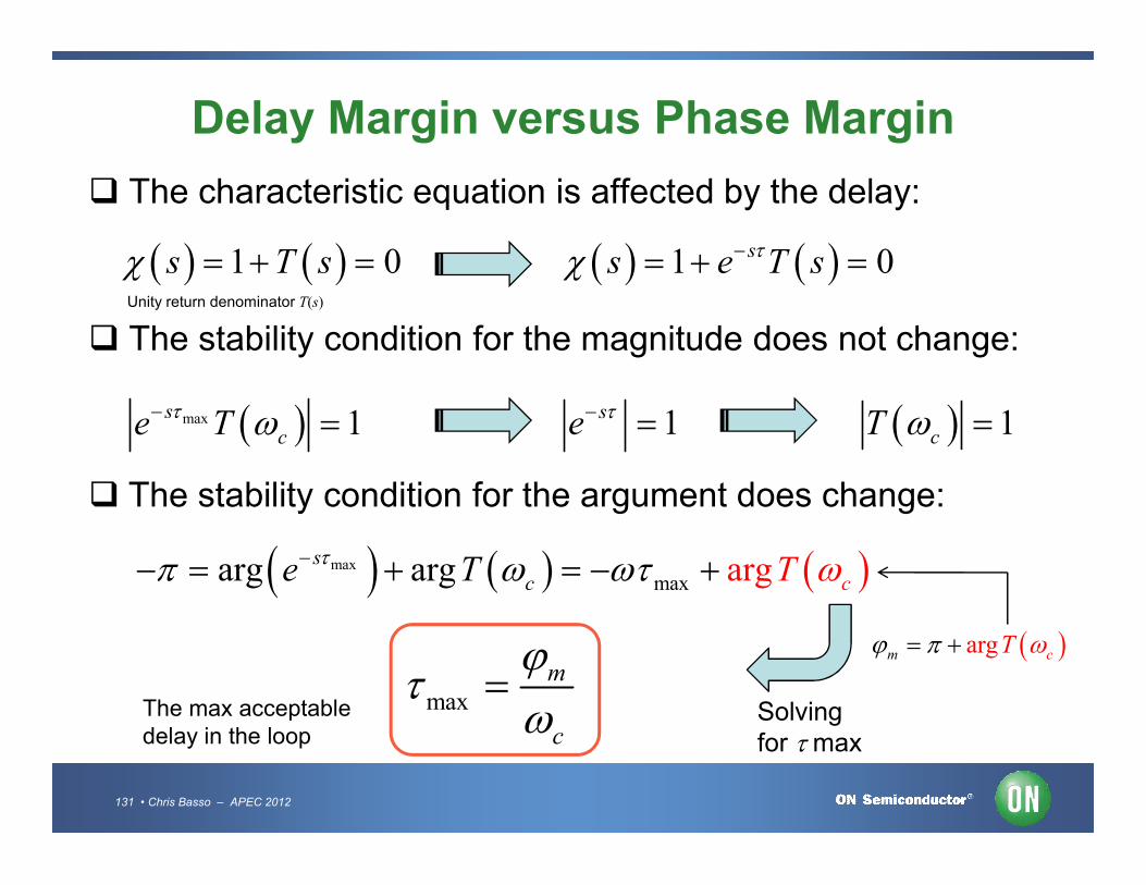
The characteristic equation is affected by the delay:
1 0ss e T s 1 0s T s
The stability condition for the magnitude does not change:
max 1sce T 1se 1cT
Unity return denominator T(s)
131 • Chris Basso – APEC 2012
1ce T 1e 1cT
The stability condition for the argument does change:
max
max aa rrg arg g cs
ce T T
argm cT
maxm
c
Solvingfor max
The max acceptabledelay in the loop
Delay Margin versus Phase Margin
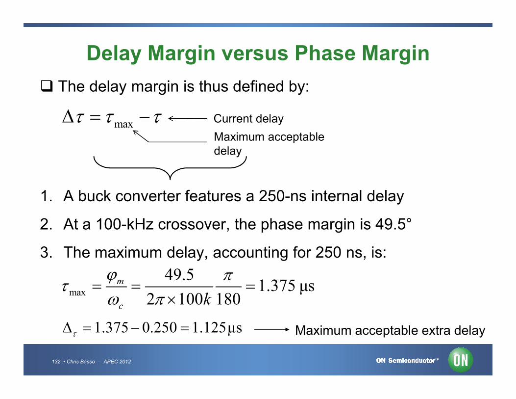
The delay margin is thus defined by:
max Current delay
Maximum acceptabledelay
1. A buck converter features a 250-ns internal delay
132 • Chris Basso – APEC 2012
1. A buck converter features a 250-ns internal delay
2. At a 100-kHz crossover, the phase margin is 49.5°
3. The maximum delay, accounting for 250 ns, is:
max
49.51.375 μs
2 100 180m
c k
1.375 0.250 1.125µs Maximum acceptable extra delay

Checking via Simulation
The delay is simply added in series with the PWM block
Vout
16
Cout
Cout
Resr
Resr
2 12
L1
Lvout
d
a c
PWM switch VM p
3
9
X1
PWMVM2
L = L
Fs = 1Meg
R6
100m
ou
t X4
Rload
2.5
Vin
10
5.00V
5.00V
5.20V5.20V
10.0V
524mV
T1TD = Tau50 = Zo
out
parameters
tau=250n
Vout
16
Cout
Cout
Resr
Resr
2 12
L1
Lvout
d
a c
PWM switch VM p
3
9
X1
PWMVM2
L = L
Fs = 1Meg
R6
100m
ou
t X4
Rload
2.5
Vin
10
5.00V
5.00V
5.20V5.20V
10.0V
524mV
T1TD = Tau50 = Zo
out
parameters
tau=250n
133 • Chris Basso – APEC 2012
10
Rupper
Rupper
Rlower
Rlower
8
V2
2.5
4
Verr
vout
13
R3
R3
C3
C3
15
R2
R2C1
C1
C2
C2
GA
IN
5
6
XPWM
GAIN
K = 0.5
X2
AMPSIMP
ino
ut X4
Config_1
LoL
1G
7
CoL
1G
V1
AC = 1
2.50V
2.50V
1.05V
5.00V
1.04V1.05V
524mV
0V
1
R150
E11
3
E21
in
10
Rupper
Rupper
Rlower
Rlower
8
V2
2.5
4
Verr
vout
13
R3
R3
C3
C3
15
R2
R2C1
C1
C2
C2
GA
IN
5
6
XPWM
GAIN
K = 0.5
X2
AMPSIMP
ino
ut X4
Config_1
LoL
1G
7
CoL
1G
V1
AC = 1
2.50V
2.50V
1.05V
5.00V
1.04V1.05V
524mV
0V
1
R150
E11
3
E21
in
Delay built with an adaptedtransmission line
Checking via Simulation
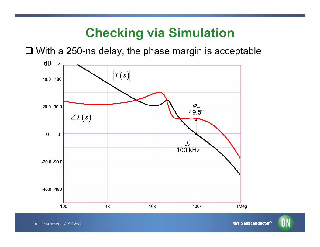
With a 250-ns delay, the phase margin is acceptable
90.0
180
20.0
40.0
dB °
T s
T s
m
49.5°90.0
180
20.0
40.0
dB °
T s
T s
m
49.5°
134 • Chris Basso – APEC 2012
100 1k 10k 100k 1Meg
-180
-90.0
0
-40.0
-20.0
0
fc
100 kHz
100 1k 10k 100k 1Meg
-180
-90.0
0
-40.0
-20.0
0
fc
100 kHz

Checking via Simulation
If we add 1.125 µs to 250 ns, no phase margin at all!
90.0
180
20.0
40.0
dB °
T s
T sm
0°
90.0
180
20.0
40.0
dB °
T s
T sm
0°
135 • Chris Basso – APEC 2012
100 1k 10k 100k 1Meg
-180
-90.0
0
-40.0
-20.0
0
4
fc
100 kHz
100 1k 10k 100k 1Meg
-180
-90.0
0
-40.0
-20.0
0
4
fc
100 kHz

Course Agenda
Introduction to Control Systems
Shaping the Error Signal
How to Implement the PID Block?
The PID at Work with a Buck Converter
Considering the Output Impedance
136 • Chris Basso – APEC 2012
Considering the Output Impedance
Classical Poles/Zeros Placement
Shaping the Output Impedance
Quality Factor and Phase Margin
What is Delay Margin?
Gain Margin is not Enough

Gain Margin Defines the Robustness
GM defines the robustness of a system to gain variations
OLT s
OLT s Conditions foroscillations:
0°0 dB
0
0dB
OL
OL
T s
T s
drift
137 • Chris Basso – APEC 2012
10 100 1k 10k 100k 1Meg
OL0°0 dB
If the gain drifts up by 38 dB, we have oscillations
20 dB/div
T f
-38 dB
1
GM 38dBT f

Gain Margin Defines the Robustness
In Bode representation but also in Nyquistm
1
2
1 GM
III
ReT
m
1
2
1 GM
III
ReT
orT s
Im 0T s
138 • Chris Basso – APEC 2012
2 1 0 1 22
1
0-1,j0
e
c
0 rd
2
T s
m
1 GM
h
III IV
2 1 0 1 22
1
0-1,j0
e
c
0 rd
2
T s
m
1 GM
h
III IV
2 2
1GM
Re ImT f T f
1
ReGM
T f
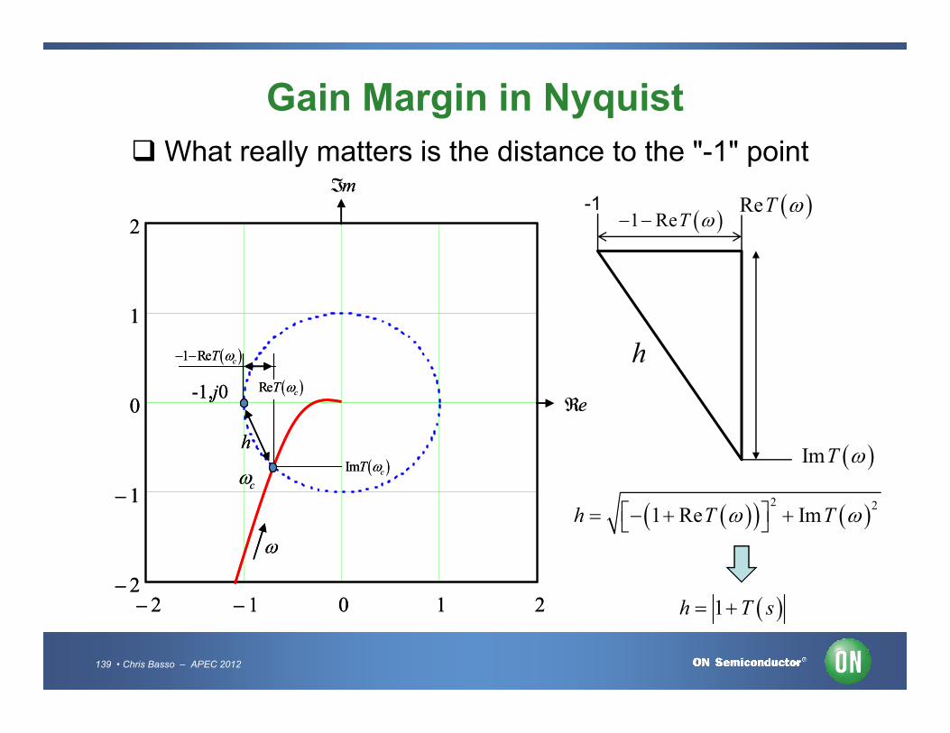
Gain Margin in Nyquist
What really matters is the distance to the "-1" point
1
2
m
1 Re cT
1
2
m
1 Re cT
-1 ReT 1 ReT
h
139 • Chris Basso – APEC 2012
2 1 0 1 22
1
0-1,j0
e
Re cT
Im cT c
h
2 1 0 1 22
1
0-1,j0
e
Re cT
Im cT c
h ImT
h
2 2
1 Re Imh T T
1h T s

Rejecting the Perturbation
H(s)u2(s) y(s)+ (s)
G(s)
+
u1(s)
H(s)u2(s) y(s)+ (s)
G(s)
+
u1(s)
A closed-loop system rejects the incoming perturbation u1
perturbation
140 • Chris Basso – APEC 2012
2 1
1
1 1
T sy s u s u s
T s T s
Sensitivity function S
1
1h T sS
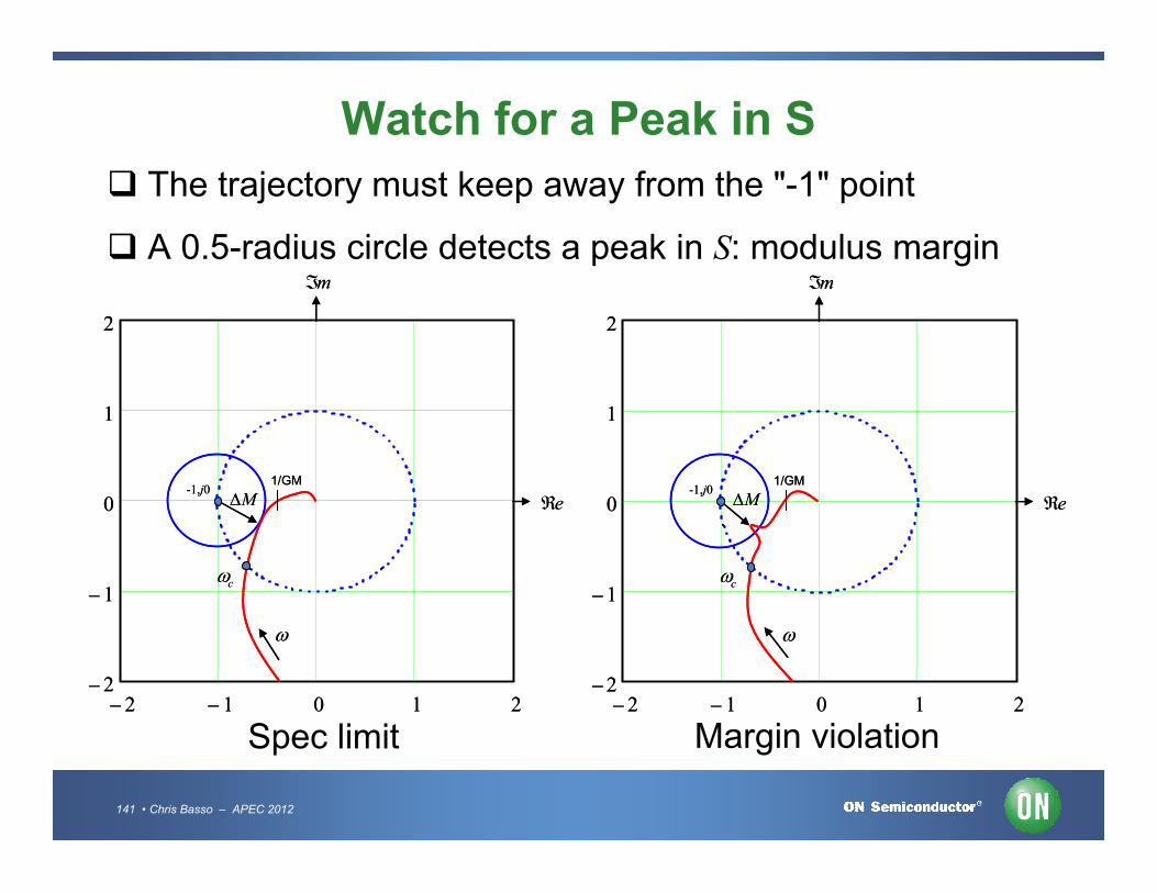
Watch for a Peak in S
The trajectory must keep away from the "-1" point
A 0.5-radius circle detects a peak in S: modulus margin
1
2
m
1
2
m
1
2
m
1
2
m
141 • Chris Basso – APEC 2012
2 1 0 1 22
1
0 e
c
-1,j0M
1/GM
2 1 0 1 22
1
0 e
c
-1,j0M
1/GM
2 1 0 1 22
1
0 e
c
-1,j0M
1/GM
2 1 0 1 22
1
0 e
c
-1,j0M
1/GM
Margin violationSpec limit
-800m -400m 0 400m 800mreal
-800m
-400m
0
400m
800m
ima
g
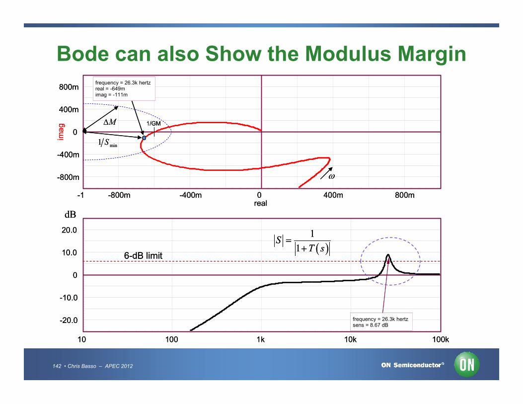
frequency = 26.3k hertzreal = -649m imag = -111m
-1
1/GMM
min1 S
-800m -400m 0 400m 800mreal
-800m
-400m
0
400m
800m
ima
g
frequency = 26.3k hertzreal = -649m imag = -111m
-1
1/GMM
min1 S
Bode can also Show the Modulus Margin
142 • Chris Basso – APEC 2012
10 100 1k 10k 100k
-20.0
-10.0
0
10.0
20.0
frequency = 26.3k hertzsens = 8.67 dB
1
1S
T s
dB
6-dB limit
real
10 100 1k 10k 100k
-20.0
-10.0
0
10.0
20.0
frequency = 26.3k hertzsens = 8.67 dB
1
1S
T s
dB
6-dB limit
real

Conclusion
Switching or linear power supplies are regulators
Applying a pure mathematical compensation brings problems
Engineering judgment found output impedance guilty
Lack of sufficient gain at resonance brings oscillations
Standard poles/zeros placement method gives good results
For high-speed dc-dc converters, resistive shaping rules
143 • Chris Basso – APEC 2012
For high-speed dc-dc converters, resistive shaping rules
Q to phase margin approximation requires engineering judgment
Less known delay and modulus margins are useful figures!
Merci !Thank you!
Xiè-xie!


![Loop Groups and twisted K-theory IIIteleman/math/finalDirac.pdfalised flag varieties of loop groups, in which twisted K-theory provides the topological side. We refer to [FHT3, x8]](https://static.fdocuments.us/doc/165x107/6124a2b9fb0dcd32184636bb/loop-groups-and-twisted-k-theory-iii-telemanmathfinaldiracpdf-alised-iag-varieties.jpg)