The CMOS Inverter · - No static power dissipation. ESD II A.A. 05/06 PMOS Load Lines V in = V DD...
42
ESD II A.A. 05/06 The CMOS Inverter The CMOS Inverter V in V out C L V DD
Transcript of The CMOS Inverter · - No static power dissipation. ESD II A.A. 05/06 PMOS Load Lines V in = V DD...

ESD II A.A. 05/06
The CMOS InverterThe CMOS Inverter
Vin Vout
CL
VDD
ESD II A.A. 05/06
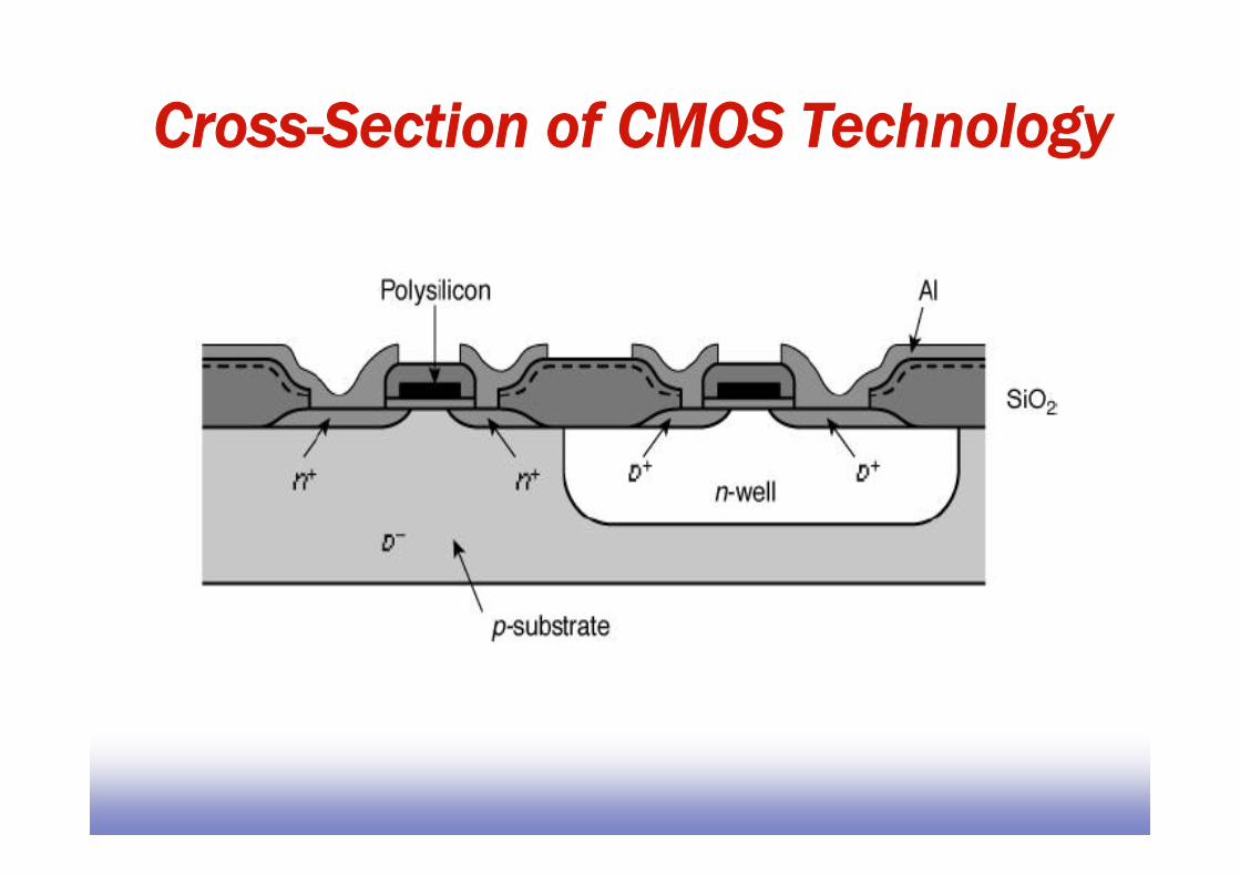
Cross-Section of CMOS Technology

ESD II A.A. 05/06
CMOS InverterCMOS InverterFirstFirst--Order DC AnalysisOrder DC Analysis
VOL = 0VOH = VDD
VM = f(Rn, Rp)
VDD VDD
Vin = VDD Vin = 0
VoutVout
Rn
Rp

ESD II A.A. 05/06
CMOS inverters in the two possible binary states
ESD II A.A. 05/06
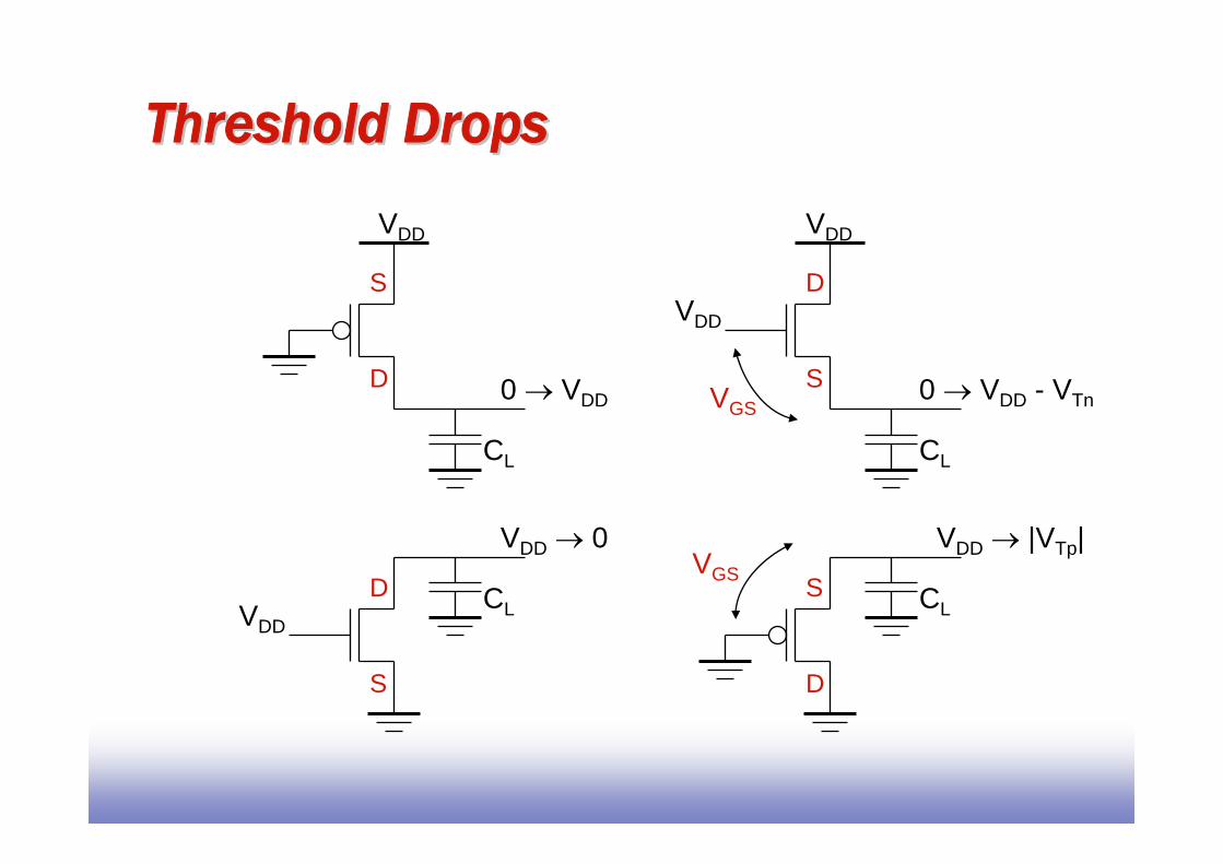
Threshold DropsThreshold DropsVDD
VDD → 0
0 → VDD
CL
CL
VDD
0 → VDD - VTn
CL
VDD
VDD
VDD → |VTp|
CL
S
D S
D
VGS
S
SD
D
VGS

ESD II A.A. 05/06
CMOS Properties
-At every point in time (except during the switching transients) each gate output is connected to either VDD or GND via a low-resistive path
- Symmetrical VTC
- No direct path exists between the supply and ground rails under steady-state operating conditions
- The steady-state input current is nearly zero
- Full rail-to-rail swing
- No static power dissipation

ESD II A.A. 05/06
PMOS Load LinesPMOS Load Lines
V in = V DD +VGSp
IDn = - I Dp
V out = V DD +V DSp
V in = V DD +VGSp
IDn = - I Dp
V out = V DD +VDSpV in = V DD +VGSp
IDn = - I Dp
V in = V DD +VGSp
IDn = - I Dp
V out = V DD +VDSpV out = V DD +VDSp

ESD II A.A. 05/06
CMOS Inverter Load CharacteristicsCMOS Inverter Load Characteristics
Vout

ESD II A.A. 05/06
CMOS Inverter VTCCMOS Inverter VTC

ESD II A.A. 05/06
CMOS VTC may be broken down into five regions

ESD II A.A. 05/06
CMOS VTC for KR = 5, 1 and 0. 2 for VDD = 5 V
ESD II A.A. 05/06
100
1010.8
0.9
1
1.1
1.2
1.3
1.4
1.5
1.6
1.7
1.8
MV(V
)
Wp/Wn
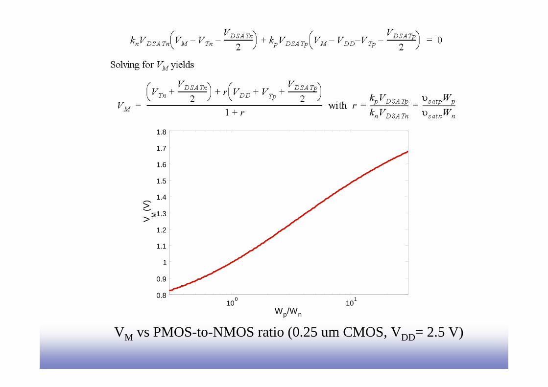
VM vs PMOS-to-NMOS ratio (0.25 um CMOS, VDD= 2.5 V)

ESD II A.A. 05/06
Changing the inverter threshold can improve the circuit reliability

ESD II A.A. 05/06
Noise margins vs KR for the CMOS inverter with VDD= 5V and VTN= -VTP= 1V

ESD II A.A. 05/06
CMOS VTC for VDD = 5 V, 4 V, 3 V and 2 V

ESD II A.A. 05/06
but it deteriorates for very low VDD
0 0.05 0.1 0.15 0.20
0.05
0.1
0.15
0.2
Vin (V)
Vou
t (V)
0 0.5 1 1.5 2 2.50
0.5
1
1.5
2
2.5
Vin (V)
Vou
t(V)
Reducing VDD improves the gain ….
(0.25 um CMOS, VDD= 2.5V)

ESD II A.A. 05/06
0 0.5 1 1.5 2 2.50
0.5
1
1.5
2
2.5
Vin (V)
Vou
t(V)
Good PMOSBad NMOS
Good NMOSBad PMOS
Nominal
Impact of device variations on static CMOS inverter VTC
(0.25 um CMOS, VDD= 2.5V)

ESD II A.A. 05/06
CMOS Inverter: Transient ResponseCMOS Inverter: Transient Response
tpHL = f(Rn .CL)= 0.69 Rn CL
V out
R n
VDD
Vin = VDD
(b) High-to-low
CL
Vout
Rp
VDD
V in = 0
(a) Low-to-high
CL
tpLH = f(Rp .CL)= 0.69 Rp CL

ESD II A.A. 05/06
High-to-low output transition in a CMOS inverter
ESD II A.A. 05/06
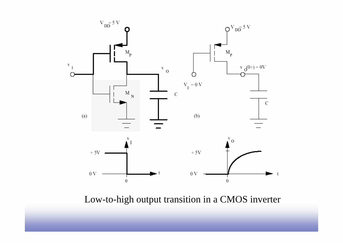
Low-to-high output transition in a CMOS inverter

ESD II A.A. 05/06
0 0.5 1 1.5 2 2.5
x 10-10
-0.5
0
0.5
1
1.5
2
2.5
3
t (sec)
Vou
t(V)
tp = 0.69 CL (Reqn+Reqp)/2tpLH
tpHL
Propagation Delay
ESD II A.A. 05/06
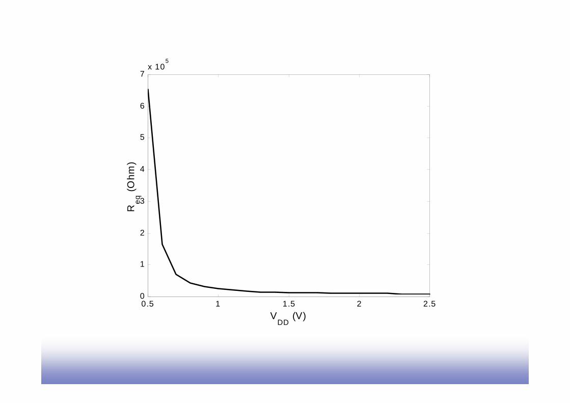
0.5 1 1.5 2 2.50
1
2
3
4
5
6
7x 10
5
VDD
(V)
Req
(Ohm
)

ESD II A.A. 05/06
0.8 1 1.2 1.4 1.6 1.8 2 2.2 2.41
1.5
2
2.5
3
3.5
4
4.5
5
5.5
VDD
(V)
t p(nor
mal
ized
)

ESD II A.A. 05/06
Parasitic CapacitancesParasitic Capacitances

ESD II A.A. 05/06

ESD II A.A. 05/06
2 4 6 8 10 12 142
2.2
2.4
2.6
2.8
3
3.2
3.4
3.6
3.8x 10
-11
S
t p(sec
)
Device SizingDevice Sizing
(for fixed load)
Self-loading effect:Intrinsic capacitancesdominate

ESD II A.A. 05/06
1 1.5 2 2.5 3 3.5 4 4.5 53
3.5
4
4.5
5x 10
-11
β
t p(sec
)NMOS/PMOS ratioNMOS/PMOS ratio
tpLH tpHL
tp β = Wp/Wn

ESD II A.A. 05/06
Input Signal RiseInput Signal Rise--Fall TimeFall Time
(for fixed load)
Propagation delay vs input signal slope

ESD II A.A. 05/06
Where Does Power Go in CMOS?Where Does Power Go in CMOS?
• Dynamic Power Consumption
• Short Circuit Currents
• Leakage
Charging and Discharging Capacitors
Short Circuit Path between Supply Rails during Switching
Leaking diodes and transistors

ESD II A.A. 05/06
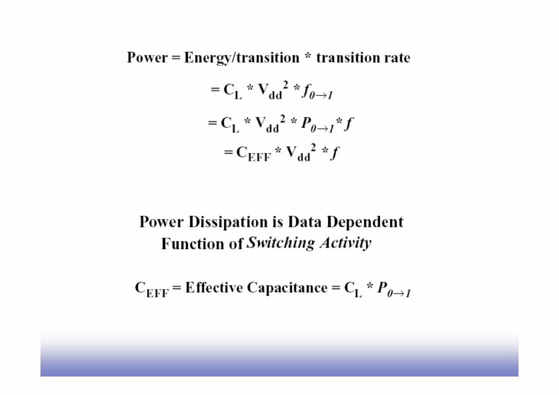
Dynamic Power DissipationDynamic Power Dissipation
Vin Vout
C L
Vdd
Energy/transition = C L * Vdd2
Power = Energy/transition * f = CL * Vdd2 * f
Need to reduce C L, Vdd, and f to reduce power.Not a function of transistor sizes!
ESD II A.A. 05/06

ESD II A.A. 05/06

ESD II A.A. 05/06
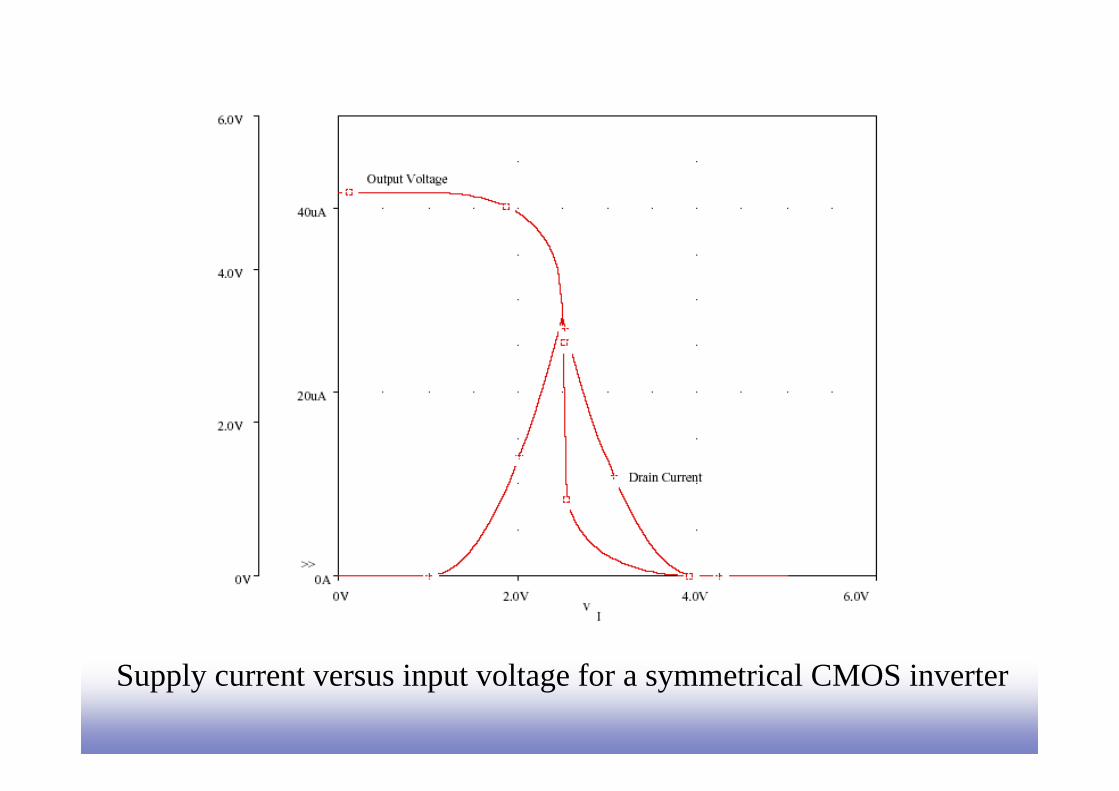
Short Circuit CurrentsShort Circuit Currents
ESD II A.A. 05/06
Supply current versus input voltage for a symmetrical CMOS inverter
ESD II A.A. 05/06
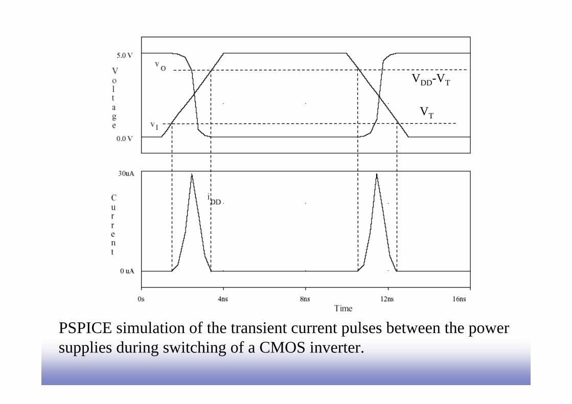
PSPICE simulation of the transient current pulses between the power supplies during switching of a CMOS inverter.
VDD-VT
VT

ESD II A.A. 05/06
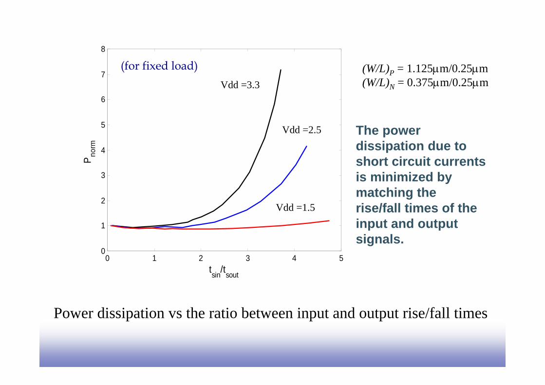
Impact of rise/fall times on short-circuit currents
ESD II A.A. 05/06
0 1 2 3 4 50
1
2
3
4
5
6
7
8
tsin/tsout
P norm
Vdd =1.5
Vdd =2.5
Vdd =3.3(W/L)P = 1.125μm/0.25μm(W/L)N = 0.375μm/0.25μm
Power dissipation vs the ratio between input and output rise/fall times
The power dissipation due to short circuit currents is minimized by matching therise/fall times of the input and output signals.
(for fixed load)

ESD II A.A. 05/06
Vout
Vdd
Sub-ThresholdCurrent
Drain JunctionLeakage
Sub-threshold current one of most compelling issuesin low-energy circuit design!
Static Power ConsumptionStatic Power Consumption

ESD II A.A. 05/06
ReverseReverse--Biased Diode LeakageBiased Diode Leakage
Np+ p+
Reverse Leakage Current
+
-Vdd
GATE
IDL = JS × A
JS = 10-100 pA/μm2 at 25 deg C for 0.25μm CMOSJS doubles for every 9 deg C!
ESD II A.A. 05/06
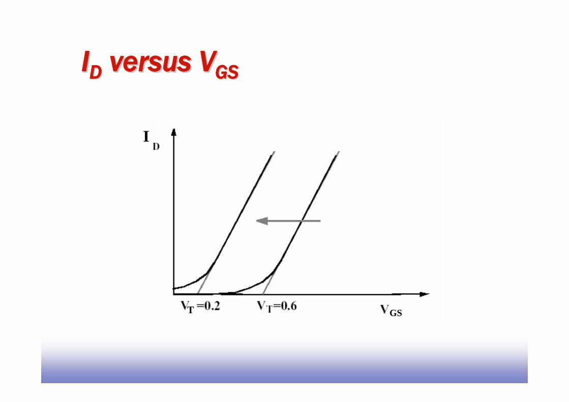
IIDD versus Vversus VGSGS
II
GST

ESD II A.A. 05/06
Subthreshold Leakage ComponentSubthreshold Leakage Component

ESD II A.A. 05/06
Principles for Power ReductionPrinciples for Power Reduction
Prime choice: Reduce voltage!
Reduce switching activity
Reduce physical capacitance