
The Challenges in Making NIL Master Templates · eBeam Initiative Luncheon at SPIE 2014 © 2011 Dai...
16
© 2011 Dai Nippon Printing Co.,Ltd. All Rights Reserved. The Challenges in Making NIL Master Templates Naoya Hayashi Dai Nippon Printing Co., Ltd. A Member of the eBeam Initiative
Transcript of The Challenges in Making NIL Master Templates · eBeam Initiative Luncheon at SPIE 2014 © 2011 Dai...

© 2011 Dai Nippon Printing Co.,Ltd. All Rights Reserved.
The Challenges in Making NIL
Master Templates
Naoya Hayashi
Dai Nippon Printing Co., Ltd.
A Member of the eBeam Initiative

eBeam Initiative Luncheon at SPIE 2014 11© 2011 Dai Nippon Printing Co.,Ltd. All Rights Reserved.
OUTLINE
Recent Progress in Nanoimprint for CMOS
Challenges in NIL master templates
Patterning challenges
Summary
eBeam Initiative Luncheon at SPIE 2016

eBeam Initiative Luncheon at SPIE 2014 22© 2011 Dai Nippon Printing Co.,Ltd. All Rights Reserved.
NIL template strategy
EB writing
Imprint
Wafer imprint
High quality
master template
Multiple replica
templates
Multiple replica templates will be duplicated from high
quality EB written master template.
Replica templates
used as stamps for
wafer lithographyMaster
Replica
eBeam Initiative Luncheon at SPIE 2016

eBeam Initiative Luncheon at SPIE 2014 33© 2011 Dai Nippon Printing Co.,Ltd. All Rights Reserved.
Template fabrication process
EB writing
Imprint
Master
Develop Etching Repair
Replica
Etching
Resolution
IP control
CDU
Uniformity Inspection
Fine repair
Defect
IP control
CDU
Uniformity
Defect
Inspection
Zero defect
master
Replica
Master Wafer imprint
eBeam Initiative Luncheon at SPIE 2016

eBeam Initiative Luncheon at SPIE 2014 44© 2011 Dai Nippon Printing Co.,Ltd. All Rights Reserved.
Comparison between Optical masks
and NIL templates
NIL template Optical/EUV mask
Lithography Near field lithography Far field lithography
Magnification X1 X4
Field size 26mmx33mm 112mmx132mm
Substrate 6025 Quartz 6025 Quartz
Mask fabrication Master: EB / Replica: NIL EB lithography
EB process High resolution / low sensitivity
/ Non-CAR
High sensitivity / CAR
Difficulties in NIL template fabrication Master template resolution and throughput are the most critical
issues for X1 lithography Defect control becomes difficult due to near field (contact)
lithography Duplication from master to replica template degrades master
template performance
eBeam Initiative Luncheon at SPIE 2016

eBeam Initiative Luncheon at SPIE 2014 55© 2011 Dai Nippon Printing Co.,Ltd. All Rights Reserved.
General performance status at
hp3x nm generation
eBeam Initiative Luncheon at SPIE 2016

eBeam Initiative Luncheon at SPIE 2014 66© 2011 Dai Nippon Printing Co.,Ltd. All Rights Reserved.
CD map of the current template
Replica Template CD uniformity
CDU(3σ) = 1.5nm
○ : -● : +
Error sources:
Master uniformity,
RLT uniformity,
Etching uniformity,
need to be optimized.
RLT
(Residual film
thickness)
Master
eBeam Initiative Luncheon at SPIE 2016
eBeam Initiative Luncheon at SPIE 2014 77© 2011 Dai Nippon Printing Co.,Ltd. All Rights Reserved.
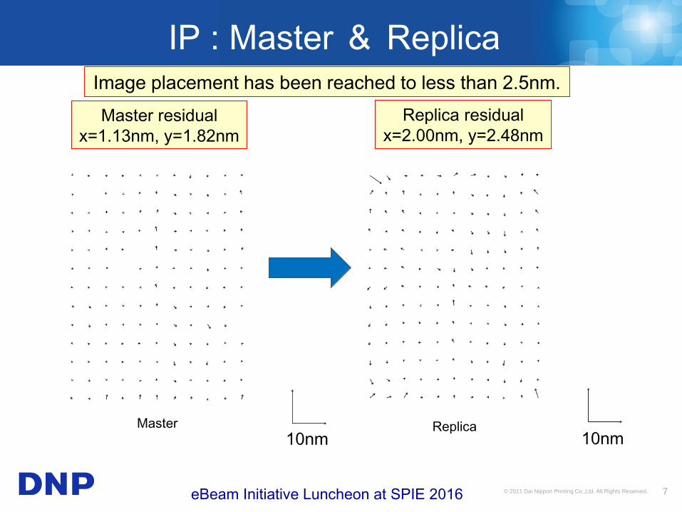
IP : Master & Replica
10nm 10nmMaster Replica
Replica residual
x=2.00nm, y=2.48nm
Image placement has been reached to less than 2.5nm.
eBeam Initiative Luncheon at SPIE 2016
Master residual
x=1.13nm, y=1.82nm

eBeam Initiative Luncheon at SPIE 2014 88© 2011 Dai Nippon Printing Co.,Ltd. All Rights Reserved.
1
10
100
1000
10000
100000
1000000
Q3 Q4 Q1 Q2 Q3 Q4 H1 H2
2011 2012 2013
DD:0.6pcs/cm2
Non-fills
Process defects
History of replica template defect improvement
2014
Master damages
Plugs
Defect density (DD) has been reduced to 0.6 pcs./cm2 by defect
source analysis and process optimization.
Defe
ct
density (
pic
s/s
q.c
m)
eBeam Initiative Luncheon at SPIE 2016

eBeam Initiative Luncheon at SPIE 2014 99© 2011 Dai Nippon Printing Co.,Ltd. All Rights Reserved.
Defect density of replica
Defect density of replica template is now less than 5 pieces/cm2
0
1
2
3
4
5
6
7
8
9
10
1 2 3 4 5 6 7 8 9 10 11 12 13 14 15 16
Defe
ct
densi
ty (
pics/
sq.c
m)
Number of replica
eBeam Initiative Luncheon at SPIE 2016

eBeam Initiative Luncheon at SPIE 2014 1010© 2011 Dai Nippon Printing Co.,Ltd. All Rights Reserved.
NIL Template Readiness
Templates are ready for use!
Target Status
Defectivity (pcs/cm2) 1.0 0.6
CD Uniformity (3σ, nm) 2.2 1.5
Image Placement (3σ, nm) 2.5 2.5
eBeam Initiative Luncheon at SPIE 2016
* Status of hp2x and 1x nm generation were updated at the morning
sessions of today.

eBeam Initiative Luncheon at SPIE 2014 1111© 2011 Dai Nippon Printing Co.,Ltd. All Rights Reserved.
Patterning Challenges
eBeam Initiative Luncheon at SPIE 2016

eBeam Initiative Luncheon at SPIE 2014 1212© 2011 Dai Nippon Printing Co.,Ltd. All Rights Reserved.
1x nm template
HP22nm HP20nm HP19nm HP18nm HP17nm
Master
Replica
1x nm replica fabrication is confirmed down to 18nm LS.
Master resolution is a key to extend NIL.
eBeam Initiative Luncheon at SPIE 2016

eBeam Initiative Luncheon at SPIE 2014 1313© 2011 Dai Nippon Printing Co.,Ltd. All Rights Reserved.
HP22nm HP20nm HP19nm HP18nm HP17nm
Master
Replica
Multi-beam Mask Writer:10nm beam resolution
EB with Non-CAR
MBMW with Non-CAR
15nm L&S
eBeam Initiative Luncheon at SPIE 2016

eBeam Initiative Luncheon at SPIE 2014 1414© 2011 Dai Nippon Printing Co.,Ltd. All Rights Reserved.
Resist images
hp14nmhp16nm hp15nm hp13nm
Resolution with 100kV EB Writer
100KeV EB
with Non-CAR
MBMW with Non-CAR
15nm L&S
Multi-beam Mask Writer:10nm beam resolution
eBeam Initiative Luncheon at SPIE 2016

eBeam Initiative Luncheon at SPIE 2014 1515© 2011 Dai Nippon Printing Co.,Ltd. All Rights Reserved.
Summary
マスター
NIL template progresses in CMOS application CD uniformity of 1.5nm has been obtained. Image placement of within 2.5nm residual distortion has
been obtained. Defect density on templates has been improved to zero
defect on master template, and <1 defect/cm2 on
replicated template at hp3x nm generation. We have
been working on further improvement on hp2x/1x nm.
Patterning challenges in master templates Resolution down to 1x nm and beyond Throughput
Promising solution Multi e-beam mask writer will provide the solution!
eBeam Initiative Luncheon at SPIE 2016


![[XLS] · Web view1 7/2/2018 1000000 100000. 2 7/2/2018 100000 100000. 3 7/2/2018 200000 200000. 4 7/2/2018 100000 100000. 5 7/2/2018 1000000 500000. 6 7/2/2018 100000 100000. 7 7/2](https://static.fdocuments.us/doc/165x107/5e9a7b97e698772c56054a6e/xls-web-view-1-722018-1000000-100000-2-722018-100000-100000-3-722018-200000.jpg)


![[XLS]reports.mca.gov.inreports.mca.gov.in/Reports/MasterDataExcels/company... · Web view100000 100000 100000 100000 10000000 430000 100000 100000 100000 100000 10000000 425000 100000](https://static.fdocuments.us/doc/165x107/5aa857b27f8b9a86188b6f26/xls-view100000-100000-100000-100000-10000000-430000-100000-100000-100000-100000.jpg)
![[XLS]reports.mca.gov.inreports.mca.gov.in/Reports/MasterDataExcels/company... · Web view500000 500000 100000 100000 100000 100000 12/3/2015 100000 100000 3/3/2015 4/3/2015 100000](https://static.fdocuments.us/doc/165x107/5a9ec0867f8b9a0d158bcbbb/xls-view500000-500000-100000-100000-100000-100000-1232015-100000-100000-332015.jpg)


![why does this suck? - University of California, Berkeleyjfc/cs160/F04/lectures/lec23/lec... · 1 10 100 1000 10000 100000 1000000 ... Graphical Excellence [Tufte] ... Example: Color](https://static.fdocuments.us/doc/165x107/5b452ae27f8b9ac6648b7ead/why-does-this-suck-university-of-california-berkeley-jfccs160f04lectureslec23lec.jpg)


