The Band (theory) Model
39
Semiconductor Physics / Micro and Nano 8th lecture Electronic properties of semiconductors The Band (theory) Model Bond model 17.May 2021
Transcript of The Band (theory) Model

7th Lecture
Semiconductor Physics / Micro and Nano
8th lecture
Electronic properties of semiconductors
The Band (theory) Model
Bond model
17.May 2021

7th Lecture
Semiconductor Physics / Micro and Nano
8th lecture
… remember the first lecture ?!
The chapter about the History of semiconductors?
7th Lecture
Semiconductor Physics / Micro and Nano 05.04.2018
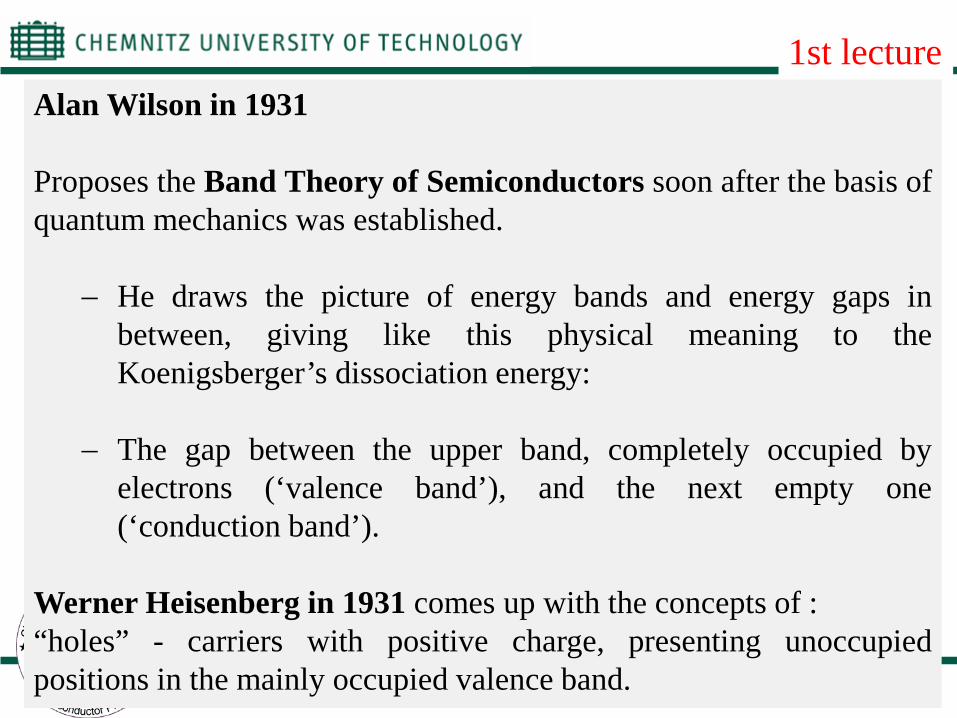
Alan Wilson in 1931 Proposes the Band Theory of Semiconductors soon after the basis of quantum mechanics was established.
− He draws the picture of energy bands and energy gaps in between, giving like this physical meaning to the Koenigsberger’s dissociation energy:
− The gap between the upper band, completely occupied by electrons (‘valence band’), and the next empty one (‘conduction band’).
Werner Heisenberg in 1931 comes up with the concepts of : “holes” - carriers with positive charge, presenting unoccupied positions in the mainly occupied valence band.
1st lecture

7th Lecture
Semiconductor Physics / Micro and Nano
Ener
gy
Conductivity 106-104 (Ωm)-1
Conductor Semiconductor Insulator
No gap
Conductivity 104-10-10 (Ωm)-1
Conductivity < 10-10 (Ωm)-1
1. General Properties of Semiconductors 1.1. Qualitative Properties
Conduction Band (CB) Valence Band (CB)
Wide gap > 6 eV Narrow gap
1st lecture
7th Lecture
Semiconductor Physics / Micro and Nano
8th lecture
…

7th Lecture
Semiconductor Physics / Micro and Nano
8th lecture The Band (theory) Model electrons in an atom occupy discrete energy levels; two atoms are in close proximity, each energy level will split into 2 due to the
Pauli exclusion principle that states that each quantum state can be occupied by no more than one electron in an electron system such as an atom molecule, or crystal;
When many atoms are brought into close proximity as in a crystal, the discrete
energy levels are replaced with bands of a semicontinuum of a very large energy states separated by gaps between the bands.

7th Lecture
Semiconductor Physics / Micro and Nano
The discrete energy states of a Si atom (a) convert or transform into energy bands in a Si crystal (b).
8th lecture
The difference between Ec and Ev is the bandgap energy or energy gap, Eg:

7th Lecture
Semiconductor Physics / Micro and Nano
the electrons tend to fill up the low energy bands first.
the lower the energy, the more completely a band is filled.
In a semiconductor, most of the lower energy bands will be totally filled; the
higher energy bands are totally empty. Between them lie two bands that are only nearly filled and nearly empty:
the valence band – top nearly filled the conduction band – low nearly filled The gap between them is called the band gap.
The electrons in a totally filled band do not have a net velocity and do not
conduct current.
A totally empty band cannot contribute to current conduction.
The valence band and the conduction band are the only energy bands that contribute to current flows in a semiconductor.

7th Lecture
Semiconductor Physics / Micro and Nano
Conduction electrons can move around in a crystal and therefore can carry electrical currents. For this reason, the conduction electrons are of more interest to the operation of devices than valence electrons.
When an electron breaks loose and becomes free leaves behind a void, or a hole. The hole can readily accept a new electron, which provides another means for electrons to move and conduct currents.
An alternative way to think of this process is that the hole moves to a new location in such case we speak of current conduction as the motion of a positive hole.
In semiconductors, current conduction by holes is as important as electron conduction in general. It is important to become familiar with thinking of the holes as mobile particles carrying positive charge, just as real as conduction electrons are mobile particles carrying negative charge.
The densities of thermally generated electrons and holes in semiconductors are generally very small at room temperature given that the thermal energy, kT, is 26 meV at room temperature.

7th Lecture
Semiconductor Physics / Micro and Nano
The band gap of a semiconductor is always one of two types:
direct band gap or indirect band gap
1st lecture
7th Lecture
Semiconductor Physics / Micro and Nano
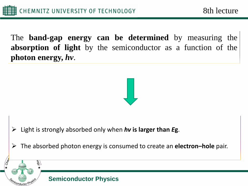
Light is strongly absorbed only when hv is larger than Eg. The absorbed photon energy is consumed to create an electron–hole pair.
The band-gap energy can be determined by measuring the absorption of light by the semiconductor as a function of the photon energy, hv.
8th lecture
7th Lecture
Semiconductor Physics / Micro and Nano
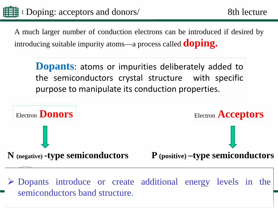
A much larger number of conduction electrons can be introduced if desired by introducing suitable impurity atoms—a process called doping.
Doping: acceptors and donors/
Dopants: atoms or impurities deliberately added to the semiconductors crystal structure with specific purpose to manipulate its conduction properties.
Electron Donors Electron Acceptors
N (negative) -type semiconductors P (positive) –type semiconductors
Dopants introduce or create additional energy levels in the semiconductors band structure.
8th lecture

7th Lecture
Semiconductor Physics / Micro and Nano
Intrinsic semiconductors Extrinsic semiconductor - dopants (impurities)
donor
acceptor
n-type (-)
p-type (+)
Bandgap Eg /eV
1. General Properties of Semiconductors 1.1. Qualitative Properties
Which goes back to Koenigsburg observation: semiconductors properties vary with impurity and defects
1st lecture

7th Lecture
Semiconductor Physics / Micro and Nano
Although less important than Ec and Ev, two other energy levels are present in the energy band diagram:
Donor energy level - Ed & Acceptor energy level - Ea
Ec – Ed = donor ionization energy
Ea – Ev = acceptor ionization energy
~20-200 meV
~20-200 meV

7th Lecture
Semiconductor Physics / Micro and Nano
The energy required to ionize a donor atom (i.e., to free the extra electron and leave a positive ion behind) may be estimated by modifying the theory of the ionization energy of a hydrogen atom:
8th lecture
m0 = free electron mass ε0 = permittivity of free space h = Planck’s constant. q = electron charge
The modification involves replacing ε0 with the relative permittivity of the material and replacing m0 with the charge carrier effective mass, meff, which is a few times smaller than m0
Because donors and acceptors have very small ionization energies, they are usually fully ionized at room temperature.

7th Lecture
Semiconductor Physics / Micro and Nano
Typical Band gap values for some relevant semiconductors
Typical Donors and Acceptors Energy values in Silicon
8th lecture
Type III Type V

7th Lecture
Semiconductor Physics / Micro and Nano
Description of motion of electrons and holes Dispersion relation & DOS
8th lecture
Assumption 2
a) To describe the motion of electrons and holes with the laws of motion of the classical particles, we must assign effective masses (mn and mp) to them because they will be different from the masses of the free particles.
Measured effective masses for different semiconductor materials
Assumption 1 The crystal is understood as a periodic coulombic field.
7th Lecture
Semiconductor Physics / Micro and Nano
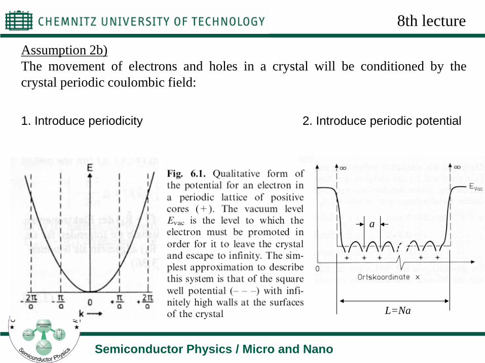
1. Introduce periodicity 2. Introduce periodic potential
a
L=Na
8th lecture
Assumption 2b) The movement of electrons and holes in a crystal will be conditioned by the crystal periodic coulombic field:
7th Lecture
Semiconductor Physics / Micro and Nano
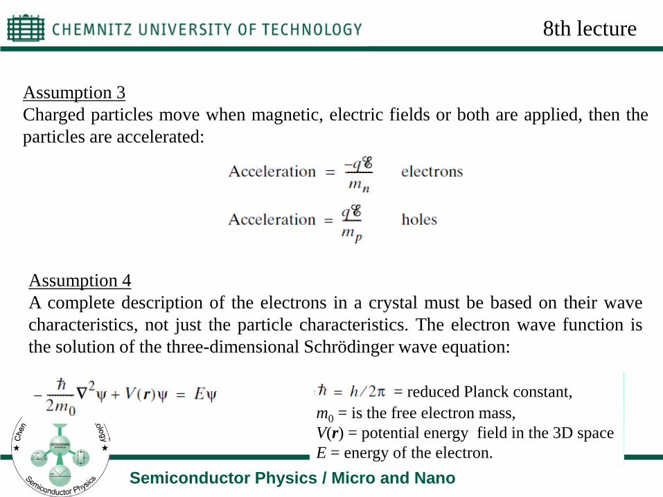
Assumption 3 Charged particles move when magnetic, electric fields or both are applied, then the particles are accelerated:
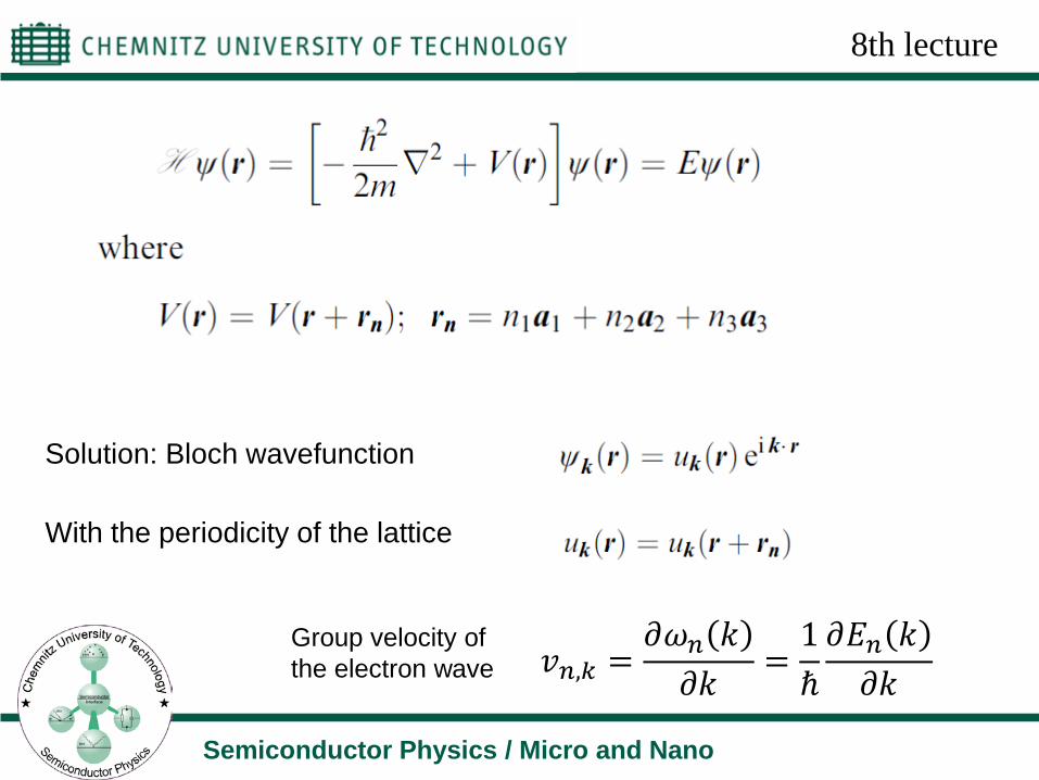
Assumption 4 A complete description of the electrons in a crystal must be based on their wave characteristics, not just the particle characteristics. The electron wave function is the solution of the three-dimensional Schrödinger wave equation:
= reduced Planck constant, m0 = is the free electron mass, V(r) = potential energy field in the 3D space E = energy of the electron.
8th lecture
7th Lecture
Semiconductor Physics / Micro and Nano
Solution: Bloch wavefunction
With the periodicity of the lattice
𝑣𝑣𝑛𝑛,𝑘𝑘 =𝜕𝜕𝜔𝜔𝑛𝑛 𝑘𝑘𝜕𝜕𝑘𝑘
=1ℏ𝜕𝜕𝐸𝐸𝑛𝑛 𝑘𝑘𝜕𝜕𝑘𝑘
Group velocity of the electron wave
8th lecture

7th Lecture
Semiconductor Physics / Micro and Nano
Resolution Method - Born-Oppenheimer or adiabatic approximation -> electrons motion independent from nucleus. - Electrons do not interact with each other free electrons - Electrons in a square box with dimensions Lx= Ly= Lz=L
8th lecture
𝜓𝜓 𝑟𝑟 =2𝐿𝐿
32
sin𝑘𝑘𝑥𝑥𝑥𝑥 ∙ sin𝑘𝑘𝑦𝑦𝑦𝑦 ∙ sin𝑘𝑘𝑧𝑧𝑧𝑧
with 𝑘𝑘𝑥𝑥 =𝜋𝜋𝐿𝐿𝑛𝑛𝑥𝑥 and 𝑛𝑛𝑥𝑥 = 1,2, … .
𝐸𝐸 =ℏ2𝑘𝑘2
2𝑚𝑚=ℏ2
2𝑚𝑚𝑘𝑘𝑥𝑥2 + 𝑘𝑘𝑦𝑦2 + 𝑘𝑘𝑧𝑧2
- , fixed boundary conditions

7th Lecture
Semiconductor Physics / Micro and Nano
Each semiconductor material has a unique E–k relationship (due to the unique V(r))
for its conduction band and another unique E–k relationship for its valence band.
Therefore, each semiconductor material has its unique mn and mp.
Energy band diagram of Germanium (Ge), Silicon (SI) and Gallium Arsenide (GaAs)
7th Lecture
Semiconductor Physics / Micro and Nano
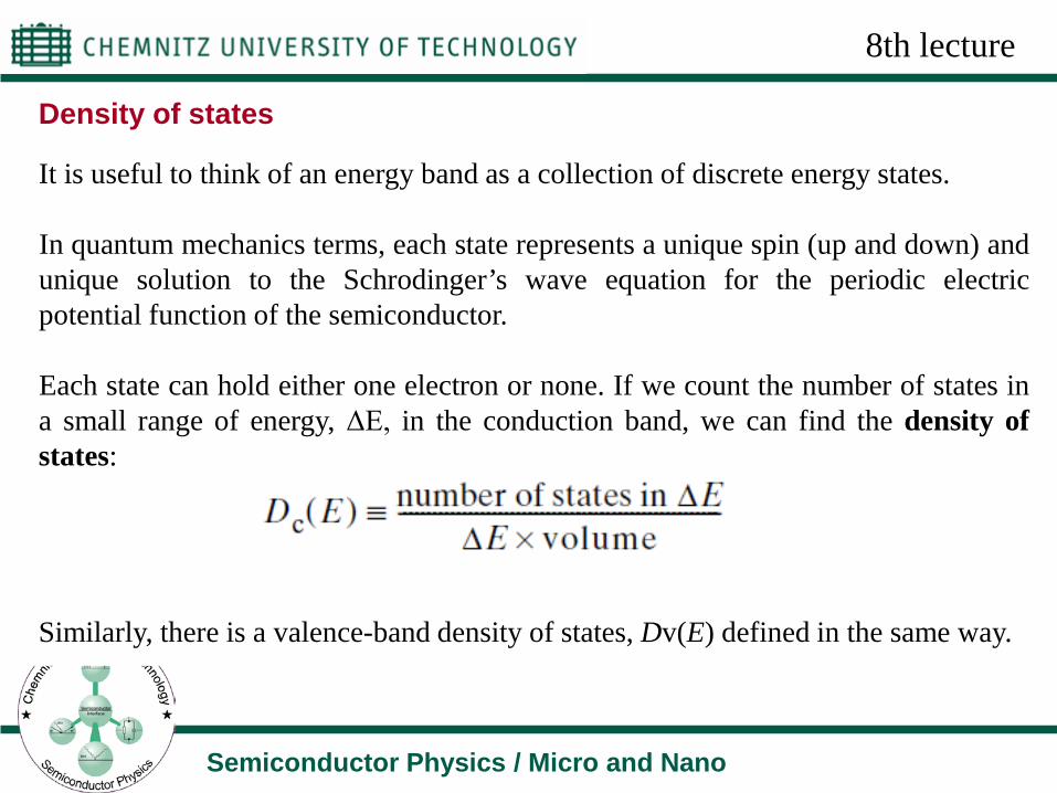
It is useful to think of an energy band as a collection of discrete energy states. In quantum mechanics terms, each state represents a unique spin (up and down) and unique solution to the Schrodinger’s wave equation for the periodic electric potential function of the semiconductor. Each state can hold either one electron or none. If we count the number of states in a small range of energy, ΔΕ, in the conduction band, we can find the density of states: Similarly, there is a valence-band density of states, Dv(E) defined in the same way.
Density of states
8th lecture

7th Lecture
Semiconductor Physics / Micro and Nano
Volume of an electronic state in the k-space
𝑉𝑉𝑘𝑘 =𝜋𝜋𝐿𝐿
3
• Nr. Of states in dE/cm3
Density of states
• ΔE -
8th lecture
7th Lecture
Semiconductor Physics / Micro and Nano
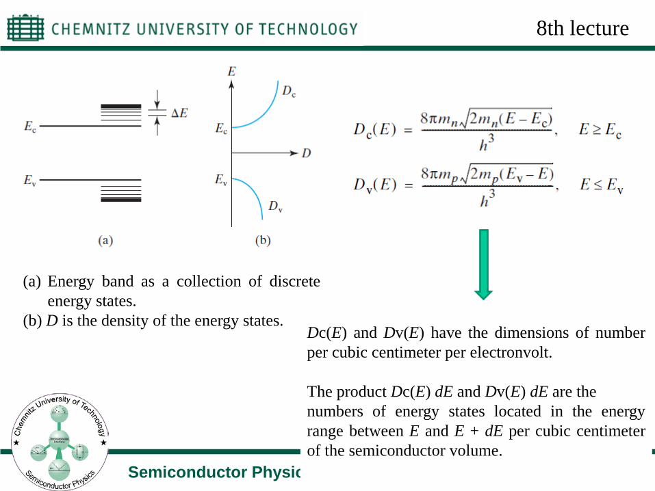
(a) Energy band as a collection of discrete energy states.
(b) D is the density of the energy states. Dc(E) and Dv(E) have the dimensions of number per cubic centimeter per electronvolt. The product Dc(E) dE and Dv(E) dE are the numbers of energy states located in the energy range between E and E + dE per cubic centimeter of the semiconductor volume.
8th lecture

7th Lecture
Semiconductor Physics / Micro and Nano
8th lecture
Thermal agitation gives each energy state a certain probability of being occupied by an electron. That probability is expressed by the Fermi function. *The Fermi function f(E) gives the probability that a given available electron energy state will be occupied at a given temperature. The Fermi function comes from Fermi-Dirac statistics and has the form: At ordinary temperatures, most of the levels up to the Fermi level EF are filled, and relatively few electrons have energies above the Fermi level. The Fermi level is on the order of a few electron volts, whereas the thermal energy kT is only about 0.026 eV at 300 K.
The Fermi Function
7th Lecture
Semiconductor Physics / Micro and Nano
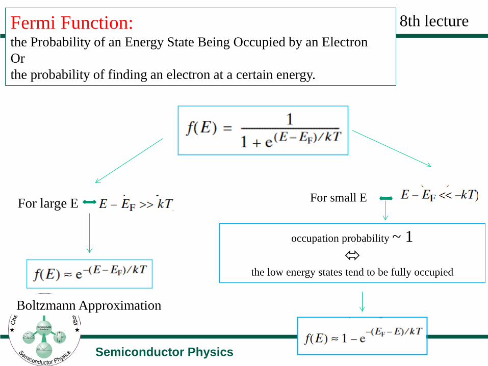
8th lecture Fermi Function: the Probability of an Energy State Being Occupied by an Electron Or the probability of finding an electron at a certain energy.
For large E
Boltzmann Approximation
For small E
occupation probability ~ 1
the low energy states tend to be fully occupied

7th Lecture
Semiconductor Physics / Micro and Nano
The Fermi function diagram
8th lecture

7th Lecture
Semiconductor Physics / Micro and Nano
Implications of the Fermi function for the electrical conductivity of a semiconductor
The band theory of solids gives the picture that there is a sizable gap between the Fermi level and the conduction band of the semiconductor. At higher temperatures, a larger fraction of the electrons can bridge this gap and participate in electrical conduction.

7th Lecture
Semiconductor Physics / Micro and Nano
Although the Fermi function has a finite value in the gap, there is no electron population at those energies (that's what you mean by a gap). The population depends upon the product of the Fermi function and the electron density of states. So in the gap there are no electrons because the density of states is zero. In the conduction band at 0 K, there are no electrons even though there are plenty of available states, but the Fermi function is zero. At high temperatures, the density of states and the Fermi function have finite values in the conduction band, so there is a finite conducting population.
SUMMARY 8th lecture

7th Lecture
Semiconductor Physics / Micro and Nano
Note that: EF is called the Fermi energy or the Fermi level
the Fermi level EF is determined by the available electrons and states
in the system. the probability of occupation at EF is Eg/2
The probability approaches unity if E is much lower than EF
The probability approaches zero at E much higher than EF A very important fact to remember about EF is that there is only one
Fermi level in a system at thermal equilibrium
In doped semiconductors, p-type and n-type, the Fermi level is shifted by the impurities, illustrated by their band gaps.

7th Lecture
Semiconductor Physics / Micro and Nano
11th lecture Fermi level: Is the term used to describe the top of the collection of electron energy levels at absolute zero temperature.
OR Is the highest energy state occupied by electrons in a material at absolute zero temperature. As the temperature is increased, electrons start to exist in higher energy states too. This concept comes from Fermi-Dirac statistics. Electrons are fermions and by the Pauli exclusion principle cannot exist in identical energy states. So at absolute zero they pack into the lowest available energy states and build up a "Fermi sea" of electron energy states. The Fermi level is the surface of that sea at absolute zero where no electrons will have enough energy to rise above the surface. The concept of the Fermi energy is a crucially important concept for the
understanding of the electrical and thermal properties of solids.
The Fermi level is referred to as the electron chemical potential in other contexts.
7th Lecture
Semiconductor Physics / Micro and Nano
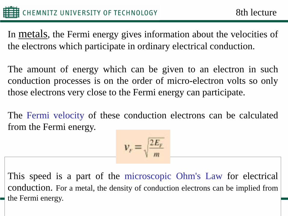
In metals, the Fermi energy gives information about the velocities of the electrons which participate in ordinary electrical conduction. The amount of energy which can be given to an electron in such conduction processes is on the order of micro-electron volts so only those electrons very close to the Fermi energy can participate. The Fermi velocity of these conduction electrons can be calculated from the Fermi energy.
This speed is a part of the microscopic Ohm's Law for electrical conduction. For a metal, the density of conduction electrons can be implied from the Fermi energy.
8th lecture
7th Lecture
Semiconductor Physics / Micro and Nano
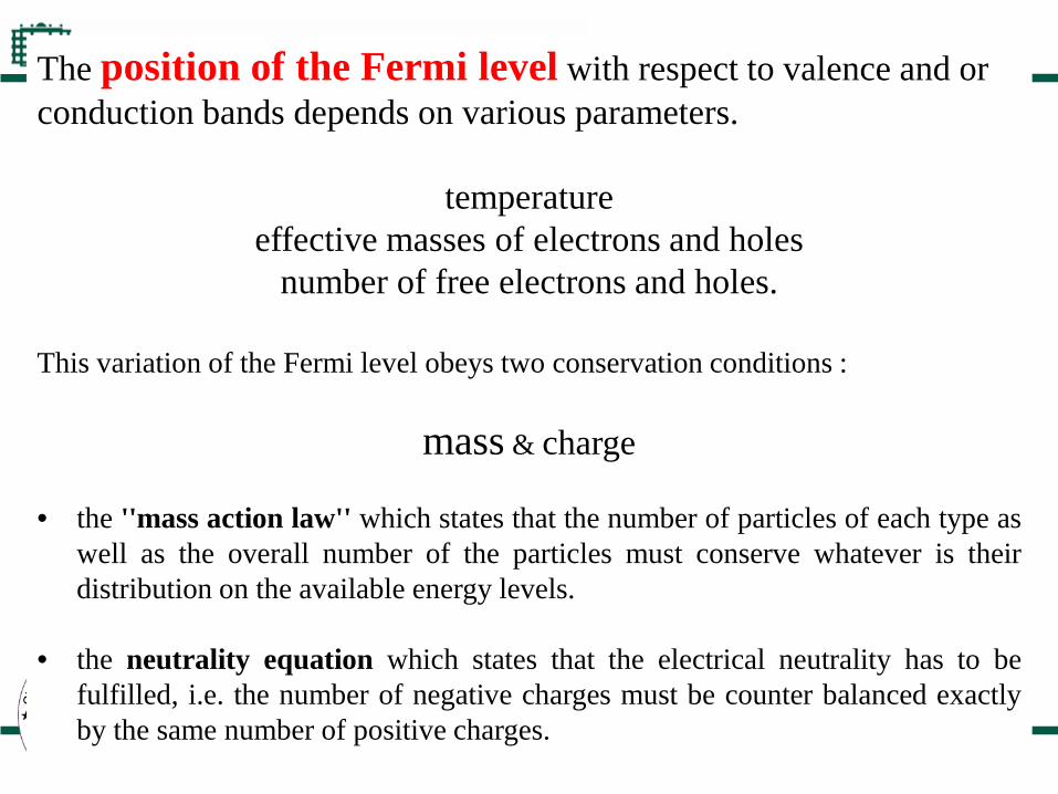
The position of the Fermi level with respect to valence and or conduction bands depends on various parameters.
temperature effective masses of electrons and holes
number of free electrons and holes. This variation of the Fermi level obeys two conservation conditions :
mass & charge
• the ''mass action law'' which states that the number of particles of each type as
well as the overall number of the particles must conserve whatever is their distribution on the available energy levels.
• the neutrality equation which states that the electrical neutrality has to be fulfilled, i.e. the number of negative charges must be counter balanced exactly by the same number of positive charges.

7th Lecture
Semiconductor Physics / Micro and Nano
The Fermi Level & Intrinsic semiconductors In an intrinsic semiconductor (with no doping at all), the Fermi level is lying exactly at the middle of the energy bandgap at T=0 Kelvin. With increasing/decreasing temperature T>0 Kelvin the Fermi
energy remains at this midgap position if conduction and valence bands have exactly the same dispersion energy or more simply the same effective masses for electrons and holes.
Or it will move towards the band with the smaller/higher effective mass, in case they are different.
8th lecture

7th Lecture
Semiconductor Physics / Micro and Nano
The Fermi Level & Extrinsic/Doped semiconductors In an extrinsic semiconductors (with added doping), in order to conserve the number of particles (mass action law) and to fulfill the overall electrical charge neutrality (neutrality equation), the Fermi level has to move away from the midgap position. It shifts towards conduction band in an n-type semiconductor (extrinsic
semiconductors with added doping impurities which are donors i.e. impurities which give additional electrons to the system) where the number of electrons n is higher than the number of holes (n>p).
It shifts towards valence band in a p-type semiconductor (extrinsic semiconductors with added doping impurities which are acceptors i.e. impurities which trap electrons from the system giving rise to a deficit of electrons or an excess of holes ) where the number of electrons n is lower than the number of holes (n<p).
8th lecture

7th Lecture
Semiconductor Physics / Micro and Nano
In reality: The electron and hole concentrations in a semiconductor are usually very different.
+ There are four types of charged species in a semiconductor: electrons, holes, positive donor ions, and negative acceptor ions. Their densities are represented by the symbols n, p, Nd, and Na.
+
In an N-type semiconductor, the abundant electrons are called the majority carriers and the almost nonexistent holes are the minority carriers.
+ In P-type semiconductors, the holes are the majority carriers and the electrons are the minority carriers.
+ The shallow donor and acceptor levels (Ed and Ea) are energy states and their occupancy by electrons is governed by the Fermi function.
+ EF cannot be close to both Ec and Ev
+ n and p cannot both be large numbers at the same time

7th Lecture
Semiconductor Physics / Micro and Nano
ELECTRON AND HOLE CONCENTRATIONS
8th lecture
What are the carrier concentrations in undoped & doped semiconductors? The np product.
These questions will be answered by relating the Fermi level and the carrier concentrations.

7th Lecture
Semiconductor Physics / Micro and Nano
Next Lecture
Electronic properties of semiconductors (cont.)
8th lecture