The apeNEXT project F. Rapuano INFN and Dip. di Fisica Università Milano-Bicocca for the APE...
35
The apeNEXT project F. Rapuano INFN and Dip. di Fisica Università Milano-Bicocca for the APE Collaboration Bielefeld University
-
Upload
osborne-dixon -
Category
Documents
-
view
215 -
download
1
Transcript of The apeNEXT project F. Rapuano INFN and Dip. di Fisica Università Milano-Bicocca for the APE...
The apeNEXT projectF. Rapuano
INFNand
Dip. di FisicaUniversità Milano-Bicocca
for the APE Collaboration
BielefeldUniversity

The Group
• Italy• Roma: N.Cabibbo, F. di Carlo, A. Lonardo, S. de Luca, D. Rossetti,
P. Vicini• Ferrara: L. Sartori, R. Tripiccione, F. Schifano• Milano-Parma: R. de Pietri, F. di Renzo, F. Rapuano
• Germany• DESY, NIC: H. Kaldass, M. Lukyanov, N. Paschedag, D. Pleiter, H. Simma
• France• Orsay: Ph. Boucaud, J. Micheli, O. Pene, • Rennes: F. Bodin

Outline of the talkapeNEXT is completely operational
and all its circuits are functioning perfectly
Mass production starting
• A bit of history
• A bit of HW
• A bit of SW
• Large installations
• Future plans

The Ape paradigm
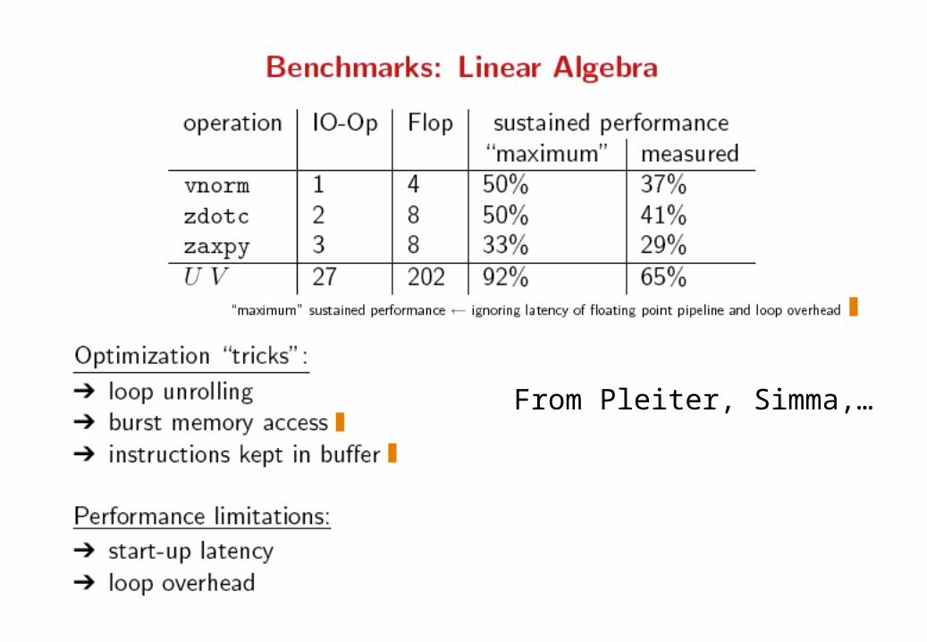
• Very efficient for LQCD (up to 65% peak), but usable for other fieldsThe “normal” operation as basic operation
a*b+c (complex)• Large number of registers for efficient optimization, Microcoded
architecture (VLIW)• Reliable and safe HW solutions• Large software effort for programming and optimization tools

“The APE family”Our line of Home Made Computers
Once upon a time (1984) italian lattice physicists were sad …
APE(1988) APE100(1993) APEmille(1999)
apeNEXT(2004)
Architecture SISAMD SISAMD SIMAMD SIMAMD+
# nodes 16 2048 2048 4096
Topology flexible 1D rigid 3D flexible 3D flexible 3D
Memory 256 MB 8 GB 64 GB 1 TB
# registers (w.size)
64 (x32) 128 (x32) 512 (x32) 512 (x64)
clock speed 8 MHz 25 MHz 66 MHz 200 MHz
peak speed 1 GFlops 100 GFlops 1 TFlops 7 TFlops
Home madeVLSI begins EU collaboration


• Lattice 2000 (Bangalore) FR, general ideas
• Lattice 2001 (Berlin) R. Tripiccione, clear ideas, VLSI design started, simulator running
• Lattice 2002 (Boston) D. Pleiter, all designs complete, most HW prototypes ready, VLSI design complete
• Lattice 2003 (Tsukuba) no talk, 6 months delay in VLSI. Delivered in December
Lattice conferences as status checkpoints

apeNEXT Architecture
• First neighbor communication network loosely synchronous (fifo based)
• = 8÷16 => 200 MB/s per channel
• Scalable 25 GFlops ÷ 7 Tflops
16 ÷ 4096 nodes
• Linux PCs as Host system
Z+(bp)
Y+(bp)
X+(cables)
0 2
4 6
8 10
12 14
1 3
5 7
9 11
13 15
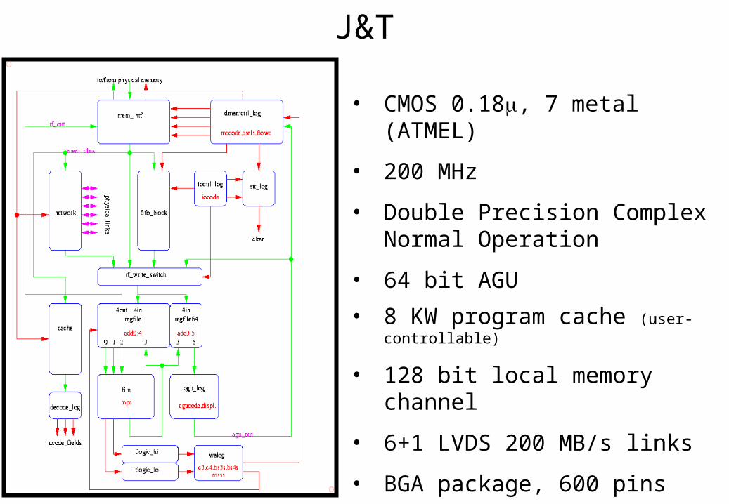
J&T
DDR-MEM
X+
………Z-
• 3D mesh of computing nodes, 64bit arithm•Custom VLSI processor - 200 MHz (J&T)
•512 registers
•1.6 GFlops per node (complex “normal”)
•256 MB ÷1 GB memory per node
•3.2 GB/s memory bandwidth (128 but chan)
•Prefetch queues
7th link

Topology
•System topologies:
- Processing Board 4 x 2 x 2 ~ 26 GF
- subCrate (16 PB) 4 x 8 x 8 ~ 0.4 TF
- Crate (32 PB) 8 x 8 x 8 ~ 0.8 TF
- Large systems (8*n) x 8 x 8
• Two directions (Y,Z) on the backplane
• Direction X through front panel cables

PB
Z+(bp)
Y+(bp)
X+(cables)
0 2
4 6
8 10
12 14
1 3
5 7
9 11
13 15
• Dominant Technologies:
– LVDS: 1728 (16*6*2*9) differential signals 200MB/s, 144 routed via cables, 576 via backplane on 12 controlled-impedance (100Ω) layers
– High-Speed differential connectors:
•Samtec QTS (J&T Module)
•Erni ERMET-ZD (Backplane)J&T
DDR-MEM
X+
………Z-
•16 Nodes 3D-Interconnected
• 4x2x2 Topology 26 Gflops, 4.6 GB Memory
• Light System:
– J&T Module connectors
– Glue Logic (Clock tree 10Mhz)
– Global signal interconnection (FPGA)
– DC-DC converters (48V to 3.3/2.5/1.8 V)
• Collaboration with NEURICAM spa7th link

J&T
Computing & control integrated
no glue logic
Reduced time for project, simulation and test of the prototype
__128

J&T the Arithmetic box
•Pipelined “normal” a*b+c (8 flops) per cycle

J&TRemote I/O
•fifo-based communication:
• LVDS
• 1.6 Gb/s per link
(8 bit @ 200MHz)
• 6 (+1) independent bi-dir links
J&T
• CMOS 0.18, 7 metal (ATMEL)
• 200 MHz
• Double Precision Complex Normal Operation
• 64 bit AGU
• 8 KW program cache (user-controllable)
• 128 bit local memory channel
• 6+1 LVDS 200 MB/s links
• BGA package, 600 pins


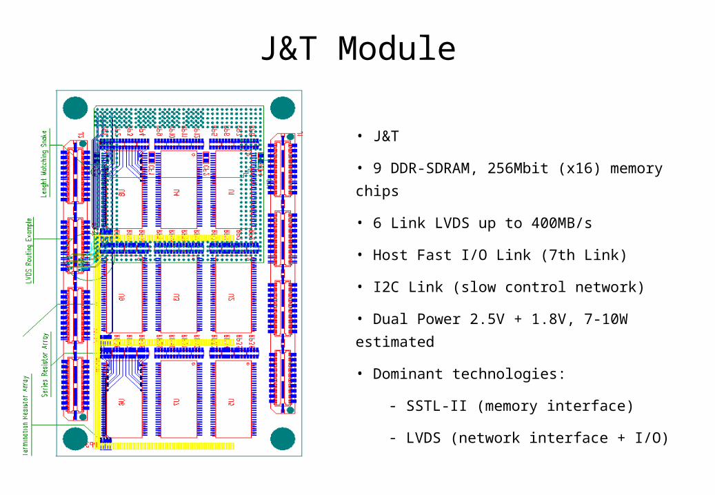
J&T Module
• J&T
• 9 DDR-SDRAM, 256Mbit (x16) memory chips
• 6 Link LVDS up to 400MB/s
• Host Fast I/O Link (7th Link)
• I2C Link (slow control network)
• Dual Power 2.5V + 1.8V, 7-10W estimated
• Dominant technologies:
- SSTL-II (memory interface)
- LVDS (network interface + I/O)


NEXT BackPlane • 16 PB Slots + Root Slot
Activity Status Who Cost Note
BP development Done APW(ERNI) 32 KEuro
BP prototypes (3) Done APW 41 KEuro
• Size 447x600 mm2•4600 LVDS differential signals,
point-to-point up to 600 Mb/s
• 16 controlled-imp. layers (32 Tot)
• Press-fit only
• Erni/Tyco connectors
•ERMET-ZD
• Providers:
APW (primary)
ERNI (2nd source)
connector kit cost: 7KEuro (!)PB Insertion force: 80-150 Kg (!)

Host I/O interface
I2C: bootstrap & control 7th-Link (200MB/s)
…

Host I/O Interface
• PCI Interface 64bit, 66Mhz
• PCI Master Mode for 7th Link Intf
• PCI Target Mode for I2C Intf
I2C (x4)
7th Link Port
PCI (64bit,66Mhz)
PCI form factor
Fifo
Altera APEXIIPCI Interface PLDA
7Link Ctrl
I2C Ctrl
PCIMaster
Ctrl
PCITargetCtrl
7Link Ctrl
QDR Mem Ctrl
Fifo
Fifo
QDRMem Bank
• QuadDataRate Memory (x32)
• Altera APEX II based
• 7th Link: 1(2) bidir chan. (200*9 M/s)
• I2C: 4 indipendent ports

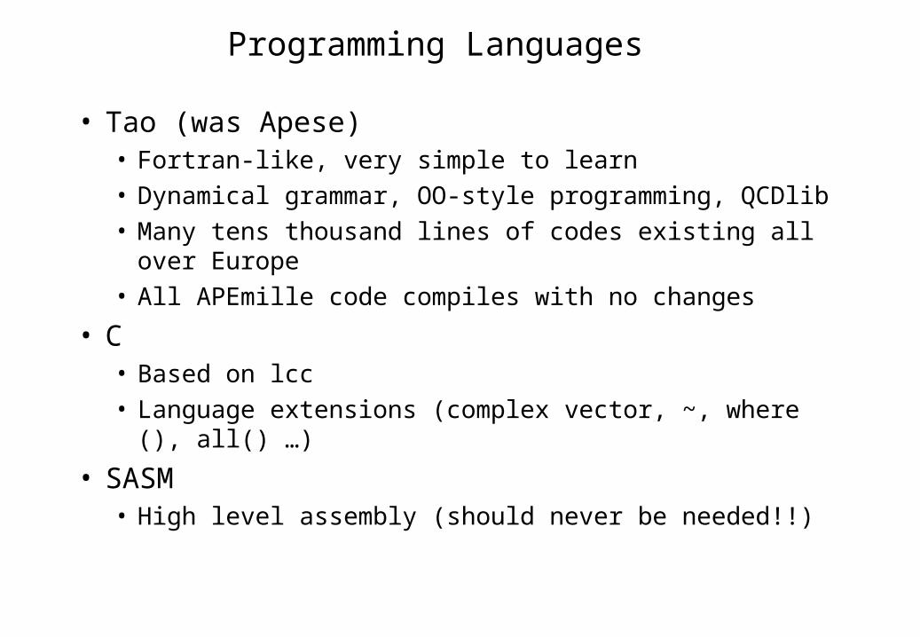
Programming Languages
• Tao (was Apese)• Fortran-like, very simple to learn
• Dynamical grammar, OO-style programming, QCDlib
• Many tens thousand lines of codes existing all over Europe
• All APEmille code compiles with no changes
• C• Based on lcc
• Language extensions (complex vector, ~, where (), all() …)
• SASM• High level assembly (should never be needed!!)
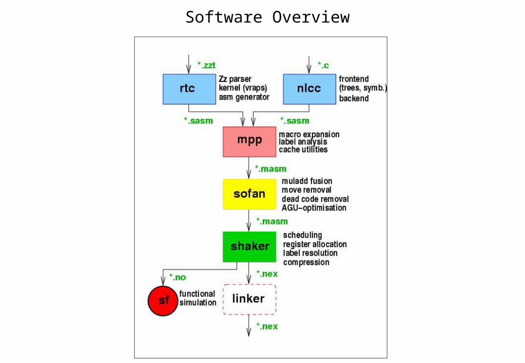
Software Overview

From Pleiter, Simma,…


Operating system
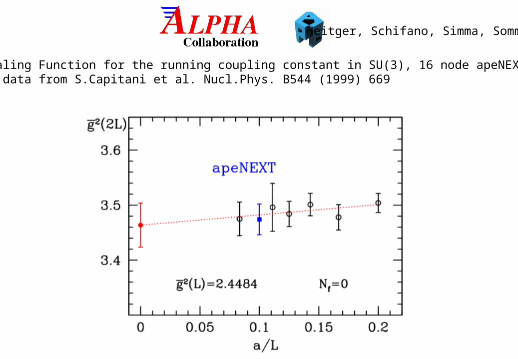
Heitger, Schifano, Simma, Sommer
Step Scaling Function for the running coupling constant in SU(3), 16 node apeNEXTNon ape data from S.Capitani et al. Nucl.Phys. B544 (1999) 669

Costs
• 1700 KEuro developments 550 KEuro + 1050 KEuro
Non VLSI VLSI
NO SALARIES
• Prototype production cost ~ 0.6-0.7 Euro/Mflops
Large scale as low as ~ 0.5, see next

• Like APEmille, apeNEXT will be commercially available.
• Slow EU procedure for offical tender (start 03/04, end ~ 08/04) to choose the company
• Committee (Vicini, Simma, FR, INFN administratives) at work
• Machines by Nov-Dec 2004 at a rate of 2x512-node/Month
• INFN has already funded apeNEXT per un totale di circa 10 Tflops in Italy to be installed at “la Sapienza”. More funds may come
• Germany and France are still contracting with their funding agencies
APEmille in Europe
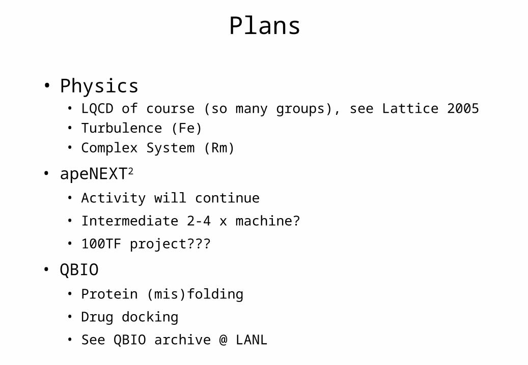
Plans
• Physics• LQCD of course (so many groups), see Lattice 2005
• Turbulence (Fe)
• Complex System (Rm)
• apeNEXT2
• Activity will continue
• Intermediate 2-4 x machine?
• 100TF project???
• QBIO
• Protein (mis)folding
• Drug docking
• See QBIO archive @ LANL