
Test of Mismatch - Home | Computer Science and …cseweb.ucsd.edu/~rtopalog/work/r2.pdf · The...
17
Test of Mismatch Rasit Onur Topaloglu and Alex Orailoglu Computer Science and Engineering Department University of California, San Diego La Jolla, CA 92093 rtopalog, alex @cse.ucsd.edu Abstract The fundamental idea of test of mismatch is to deterministically test analog circuits for the presence of mismatch. We propose an approach for testing of mismatch that delivers a compact and low-cost test set that is specialized in deterministically deciding whether a circuit has mismatch or not. This mismatch specialized test set will potentially help reduce the superfluous and time consuming functional test vector sets that have been previously used for testing analog circuits. The proposed technique enforces a separation between design and test of circuits to account for IP protection and production burst. Proper testing of mismatch will decrease test time and cost. Test set generation methodologies introduced here efficiently detect mismatch in high-end analog circuits. The proposed method is general and is applicable to a broad range of circuits. 1 Introduction The general approach underlying the test of a device should not be solely to test it for understanding whether it is working functionally or not. If this were the case, digital circuits would still be tested by purely observing their functional response. Instead they are tested for specific purposes, such as whether they have stuck-at lines. While testing digital circuits for stuck-at faults, other faulty behaviors are typically discovered in the process. One reason that digital stuck-at fault test is successful is due to the fact that most faults can be captured through stuck-at nodes. An additional reason is that most other faults can also be caught when we test the circuit using stuck-at fault test only. This flow of ideas has led us to consider the development of a similar approach for analog circuits. The logical correspondence to a stuck-at fault in digital circuits is mismatch in analog circuits, the analogy being related to the importance of their effects on the malfunctioning of the circuit. A second analogy can be construed when one considers the fact that as stuck-at test also catches other ancillary faults most of the time, so does the test
-
Upload
truongminh -
Category
Documents
-
view
214 -
download
0
Transcript of Test of Mismatch - Home | Computer Science and …cseweb.ucsd.edu/~rtopalog/work/r2.pdf · The...

Test of Mismatch
Rasit Onur Topaloglu and Alex Orailoglu
Computer Science and Engineering DepartmentUniversity of California, San Diego
La Jolla, CA 92093�rtopalog, alex � @cse.ucsd.edu
Abstract
The fundamental idea of test of mismatch is to deterministically test analog circuits for the presence of mismatch.
We propose an approach for testing of mismatch that delivers a compact and low-cost test set that is specialized in
deterministically deciding whether a circuit has mismatch or not. This mismatch specialized test set will potentially
help reduce the superfluous and time consuming functional test vector sets that have been previously used for
testing analog circuits. The proposed technique enforces a separation between design and test of circuits to
account for IP protection and production burst.
Proper testing of mismatch will decrease test time and cost. Test set generation methodologies introduced here
efficiently detect mismatch in high-end analog circuits. The proposed method is general and is applicable to a
broad range of circuits.
1 Introduction
The general approach underlying the test of a device should not be solely to test it for understanding whether it
is working functionally or not. If this were the case, digital circuits would still be tested by purely observing their
functional response. Instead they are tested for specific purposes, such as whether they have stuck-at lines. While
testing digital circuits for stuck-at faults, other faulty behaviors are typically discovered in the process. One reason
that digital stuck-at fault test is successful is due to the fact that most faults can be captured through stuck-at nodes.
An additional reason is that most other faults can also be caught when we test the circuit using stuck-at fault test
only.
This flow of ideas has led us to consider the development of a similar approach for analog circuits. The logical
correspondence to a stuck-at fault in digital circuits is mismatch in analog circuits, the analogy being related to
the importance of their effects on the malfunctioning of the circuit. A second analogy can be construed when
one considers the fact that as stuck-at test also catches other ancillary faults most of the time, so does the test

methodology proposed here. The result of these ideas has evolved into a methodology that we denote as the test
of mismatch, abbreviated as TOM.
For analog circuits, the main problem caused by mismatch is performance degradation. Unlike digital circuits, a
circuit experiencing performance degradation may still output reasonable signals for some of its output functions.
For example, a circuit outputting a good enough gain but experiencing a lower than expected output resistance
could be a typical mismatch-effected circuit. Unlike a hard fault, this circuit still outputs a good enough gain
function, but experiences different performance problems for some of its other functions.
The naive approach would be to test all functions exhaustively, as is usually done, to measure performance
parameters. The approaches presented in this paper use a rather different approach.
As this paper aims at resolving the issue of mismatch detection, we will be denoting a circuit having mismatch
as a faulty circuit. The purpose of this study is to generate the test vector set that will identify the faulty and
fault-free circuits.
2 Previous Work
Vector generation techniques have been quite successful for digital circuits. The reasons are quite apparent. As
a reminder, the assignability of a certain signal flow to the circuit and the possibility of assigning a binary value
to a signal at a node have allowed researchers to develop algorithms that detect faults in an effective manner. Test
vector generation has typically had little to do with the design of the circuit, absolving the test engineer of the
necessity of knowing much about the design.
Apparently, a similar approach would have been quite a success in the analog domain. The closest approach
has been the introduction of inductive fault analysis (IFA) [1]. However, IFA is only appropriate for physical
defects and cannot cope with performance degradation effects, which constitute the core of mismatch. Another
disadvantage of IFA is that a tremendous amount of simulations needs to be run to construct fault dictionaries,
thus inheriting has the shortcomings of any general dictionary-based testing approach.
Previous general analog test approaches mainly consist of HW modifications [10] or DSP-related approaches
[8], both of which are sometimes infeasible to attain and usually costly to implement.
Today, analog circuits are still tested largely by functional test [2]. As analog circuits can have quite a number
of high level specifications, like the gain-bandwidth product, or output resistance, the test of all these parameters
consumes a considerable amount of time. Additionally, most of these specification tests require a very expensive
high-end tester.
As shown in [3], most of these functional tests overlap, in the sense that the faulty part causing one specification
to fail also shows its effects in another parameter. To exploit this observation, an approach has been proposed

consisting of the reordering of functional test vectors. Although it reduces test time, this approach can not deal
with parametric degradations.
3 The Goals of TOM
A comparison of the digital to the analog domain yields the observation that in the analog domain, observability
and controllability constitute a much larger problem. Setting voltages or currents inside a circuit necessitates
design knowledge.
A better test methodology, however, should assume that the test engineer is just given a black box, with the
relevant specifications as to how the circuit works. Given such an input, test vectors need to be created. Such an
approach is bound to decrease the analysis time of the design, as well as protect the propriety of the design. It
will also enable the separation of testing and design, allowing intellectual property transfer between the concerned
parties.
At this point, it will be beneficial to introduce the 4 principles of the TOM vector generation methodology we
propose:
1) Low cost test : The cost of test can manifest itself in various ways. One cost is the price of the tester. If high
end functional tests are required, a multi-million dollar high-end tester will have to be used. Still, an improper
selection of test vectors will cause a great deal of cost in terms of time. As opposed to current test methodologies,
the proposed test methodology aims at getting rid of the necessity to use an expensive tester, in addition to reducing
test time considerably.
2) Separation of design from test : As designs get more and more complex, the analysis of the circuits is getting
tougher. We should not expect the test engineer to spend the predominant portion of his time on analyzing and
understanding the circuit in order to create test vectors.
3) Deterministic test : One of the fundamental reasons of success of digital test is its provision of a deterministic
pass and fail mechanism for the chips tested. The aim of our test mechanism is to be deterministic as opposed to
being probabilistic [9], notwithstanding the fact that the phenomenon of mismatch is probabilistic in its essence.
4) Self-adequacy : As mismatch is a parametric fault, the deterministic detection of mismatch gives way to the
detection of all hard faults as well. So the test vector set provided here should not be seen as an additional burden
on top of functional test, as the TOM vector set will be replacing the functional test vectors. Full fault coverage is
aimed for in light of this.
BIASVT
+
−
+
−
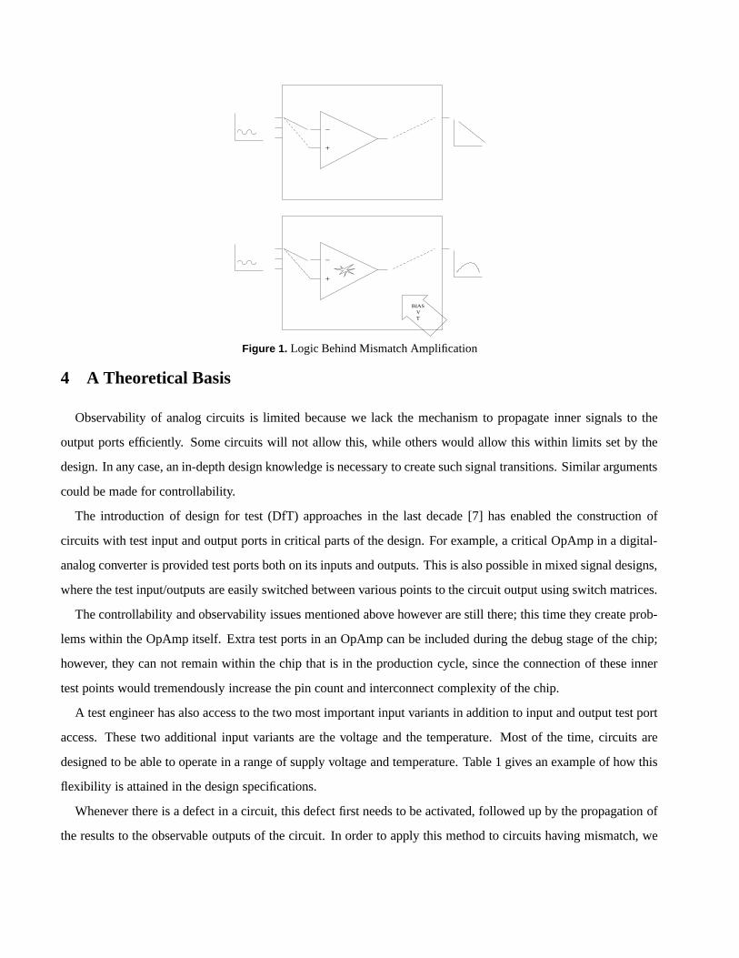
Figure 1. Logic Behind Mismatch Amplification
4 A Theoretical Basis
Observability of analog circuits is limited because we lack the mechanism to propagate inner signals to the
output ports efficiently. Some circuits will not allow this, while others would allow this within limits set by the
design. In any case, an in-depth design knowledge is necessary to create such signal transitions. Similar arguments
could be made for controllability.
The introduction of design for test (DfT) approaches in the last decade [7] has enabled the construction of
circuits with test input and output ports in critical parts of the design. For example, a critical OpAmp in a digital-
analog converter is provided test ports both on its inputs and outputs. This is also possible in mixed signal designs,
where the test input/outputs are easily switched between various points to the circuit output using switch matrices.
The controllability and observability issues mentioned above however are still there; this time they create prob-
lems within the OpAmp itself. Extra test ports in an OpAmp can be included during the debug stage of the chip;
however, they can not remain within the chip that is in the production cycle, since the connection of these inner
test points would tremendously increase the pin count and interconnect complexity of the chip.
A test engineer has also access to the two most important input variants in addition to input and output test port
access. These two additional input variants are the voltage and the temperature. Most of the time, circuits are
designed to be able to operate in a range of supply voltage and temperature. Table 1 gives an example of how this
flexibility is attained in the design specifications.
Whenever there is a defect in a circuit, this defect first needs to be activated, followed up by the propagation of
the results to the observable outputs of the circuit. In order to apply this method to circuits having mismatch, we

Table 1. Circuit Input Specification SummaryMin Typical Max Unit
Supply Voltage 2.5 2.6 2.7 VTemperature -30 27 130 C
Signal Frequency 10k 100M 1G Hz
have devised an analogous method specialized for them. This method is called mismatch amplification. The main
idea is illustrated in Figure 1. The aim is to amplify the effects of mismatch by properly activating it through some
input mechanism, then to observe the results through an output mechanism being supplied. The relevant input and
output mechanisms are discussed next.
One merit of a specialized test for mismatch is that test vectors can also detect hard faults. The underlying
reason is the fact that mismatch caused errors are performance related, while hard faults are mostly catastrophic.
4.1 Choice of Input Mechanism
In many designs, simulations of the circuits are performed under various process, voltage and temperature
corners, commonly abbreviated as PVT corners. If we relate its significance to our problem, both voltage and
temperature can be input to the circuit artificially. The third variable, in our case, the mismatch caused by the
process, is already present.
In addition, the circuit may have a number of bias inputs. These can as well be used as part of our input
mechanism assuming we have access to these ports by test ports. If they do not exist, this will not have any
deteriorating effect in our test mechanism and the proposed test methods will still be applicable.
Having figured out the input mechanism for testing the circuit, analysis mechanisms should also be identified.
This runs parallel to the general idea of testing, that of stimulating a circuit by inputs, and analyzing the effects.
When there is mismatch, the results will change appreciably. The aim of our approach is to find the least number
of vectors that makes the detection of mismatch possible, while making no concessions in fault coverage.
4.2 Choice of Analysis Methods
The choices for comparison used in TOM are comprised of AC analysis, DC analysis, pole-zero analysis,
transient analysis, IDDQ analysis and sensitivity analysis. The first three boil down to the analysis of the transfer
function. One thing that makes transfer functions useful is that they are universal and that they can be applied to
almost any circuit. Its constituents are the well known magnitude response and phase response.
Experimentation with these analysis techniques has been performed by artificially creating mismatch in bench-
mark circuits and analyzing the results of the faulty (with mismatch) and fault-free (without mismatch) circuits.
The primary criterion is the cost of the test. Generally speaking, a tester that has the capability of accurately

observing phase is very expensive. On the other hand, we have observed experimentally that the difference in
phase response between faulty and fault-free responses is rather insignificant in most cases. Since we are seeking
determinism in our test mechanism, an accurate phase response measurement would have been necessary to detect
mismatch using phase responses. The limited utility and the necessary high cost have resulted in phase responses
being excluded from TOM.
The differences in magnitude response, however, are rather large and significant. The faulty and fault-free
responses are easily separable by even a visual inspection of the results. Besides, this difference becomes so much
intensified depending on the frequency in AC analysis.
In addition to AC magnitude response, we include DC analysis in order to cope with the effects of mismatch in
digital circuits in particular. The reason is that in digital circuits, mismatch shows its effects by causing the wrong
transitions [5].
Pole-zero analysis on the other hand is not included as it would require test equipment that is quite expensive.
Although pole-zero analysis theoretically could have been used, simulations that we have conducted show that
non-dominant poles or zeros can complicate the detection of mismatch, thus causing one of the primary goals of
our system, that of being deterministic, to fail at large.
The success of IDDQ test in the digital domain is used to advantage for the analog domain in our system. This
advantage stems from the observation that IDDQ results differ significantly between faulty and fault-free circuits.
In all of the above tests, we have observed that the results differ between fault-free and faulty responses, enabling
us to easily separate a faulty and fault-free circuit.
As RF IC design is increasing its pace everyday and as more circuits are designed in the GHZ range, transient
analysis would require very accurate and expensive testers. Luckily, the differences between faulty and fault-free
results is quite small in transient analysis in most circuits. These points preclude the inclusion of a transient
analysis mechanism in the proposed test generation system.
The notion of sensitivity analysis, as implemented in SPICE, is that of measuring the output sensitivity as
compared to the changes in any of the circuit inputs. We have modified this, and instead have used sensitivity to
measure the differences of the chosen analysis techniques presented so far as compared to the changes in circuit
bias inputs. The inclusion of sensitivity thus necessitates the replication of each analysis method once more for
the changes of each bias inputs.
To give an example for the application of sensitivity to the analysis of AC magnitude response, let’s assume that
we have two current biases connected as input to our circuit. In order to measure the sensitivity of AC magnitude
response for the first bias current, we have to perturb this current by a small amount and observe the difference.
We repeat this procedure for the second bias current to end up with four analysis results. The implication of the

15.8
15.9
16
16.1
16.2
15.8
15.9
16
16.1
16.20
2
4
6
8
10
12
14
width of M1 (um)
Gain @100kHz
width of M0 (um)
Figure 2. AC Gain Sampled at 100 kHz vs. widths of a mismatch pair scanned between 15.84 � m and 16.16 � m
sensitivity technique is that the effects of mismatch can manifest themselves not directly in the response, but in
the first order derivative of the response. This derivative differ quite a lot whenever the circuit is faulty.
In DC analysis only, sensitivities are not used, as it is observed that sensitivities do not make a noticable
difference in faulty and fault-free results.
4.3 Generation of Test Vectors
Process variations are always present, but they may or may not necessarily lead to mismatch. For example, let’s
have two transistors that have to be matched. Let’s assume their widths are 16 � m. Assume that there is a process
variation over the wafer that sets each one to 15 � m. In our study, we regard such a situation as not constituting a
mismatch. However if the two are different, then we say that there is a mismatch.
The reason for making such a distinction is dependent on the performance for these two cases. The nature of
this discrepancy can be understood better by examining the experimental data shown in Figure 2. Whenever the
widths of M0 and M1, which are the two transistors to be matched in the circuit, increase and decrease equally
from their nominal values of 16 � m, the change in gain is negligible. This corresponds to the case with process
variation causing no mismatch. Whenever we are away from the line passing from origin and nominal point, there
is a big difference between the nominal value of gain and the observed value. Any part of this region corresponds
to having mismatch. We denote plots like the one in Figure 2 as excitation plots.
To verify that this sharp drop-off is still present on either side of the line through the origin, the range of M0
and M1 is increased and the same parameter is plotted in Figure 3. The only difference that can be observed is
that the gain happens to be different when the widths get smaller at the same time. This does not usually indicate
that our circuit could be designed better. Rather the reduction in the widths of both transistors would cause the

05
1015
2025
30
0
5
10
15
20
25
300
5
10
15
20
25
width of M0 (um)
Gain @ 100kHz
width of M1 (um)
Figure 3. AC Gain Sampled at 100 kHz vs. widths of a mismatch pair scanned between 2 � m and 30 � m
deterioration of some other circuit parameter such as the input resistance of the circuit. The point that needs notice
here is that there is nonetheless a sharp drop-off on both sides.
The widths of the transistors are chosen for the horizontal axes of the plot because width is a physical parameter.
The cause of mismatch is known to be physical [4]. To account for this, similar plots for the same mismatch pair
are obtained for the remaining physical parameters that are known to cause mismatch.
To possibly further amplify the effects of mismatch, one needs to include the design space flexibility as defined
in the circuit specifications. This is done by using the ranges defined for voltage sources and temperature, such
as ones in Table 1. To reduce the number of simulations, only worst-case points for the voltage and temperature
combinations should be considered. Another supporting reason for this choice is that these parameters do not
effect the circuit functions drastically but rather gradually.
Mismatch groups are provided to the test engineer by the designer. Some of these groups may contain more
than two transistors. In such a case, it is not possible to plot the effects of a physical parameter on all the transistors
in the same mismatch group. For this reason, each such plot for all mismatch pairs in a mismatch group is plotted
individually, giving
��� ���plots if the mismatch group has n transistors.
Figure 4 shows the effects on the overall frequency domain in the above case when the same set of data is used
as in the previous figures. As can be observed, at high frequencies, both faulty and fault-free signals approach
each other and it is becoming impossible to differentiate the two kinds of results from each other. However at
lower frequencies, there is a vast space between faulty and fault-free responses. At low frequencies, a bunch of
responses are gathered together at a higher gain band. Each response in this group can be recognized as constituting
a response that would be expected from a fault-free opamp. The responses in this group correspond to process
variations with no mismatch.

Figure 4. Frequency Response; widths of a mismatch pair scanned between 15.84 � m and 16.16 � m
In the DC domain, again faulty and fault-free responses are separated as can be seen in Figure 5. This time,
fault-free responses are gathered together in the left branch in the figure. The corresponding test signal should aim
at this DC range where fault-free and faulty responses are distinctly separated.
Volta
ges (
lin)
0
200m
400m
600m
800m
1
1.2
1.4
1.6
1.8
2
2.2
2.4
2.6
2.8
Voltage X (lin) (VOLTS)
1.1 1.12 1.14 1.16 1.18 1.2
*outopa
Figure 5. DC Response; widths of a mismatch pair scanned between 15.84 � m and 16.16 � m
To summarize, the test generation methodology consists of obtaining similar plots for each mismatch pair, for
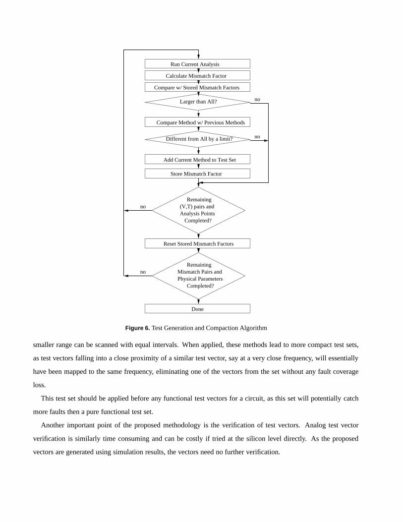
each physical parameter and for all worst-case (V,T) combinations. The algorithm is shown in Figure 6.
Having observed the drop-off, the aim in generating the test vectors consists of finding the vectors that amplify
this drop-off for each mismatch pair and each physical parameter. In order to measure and automate the calculation
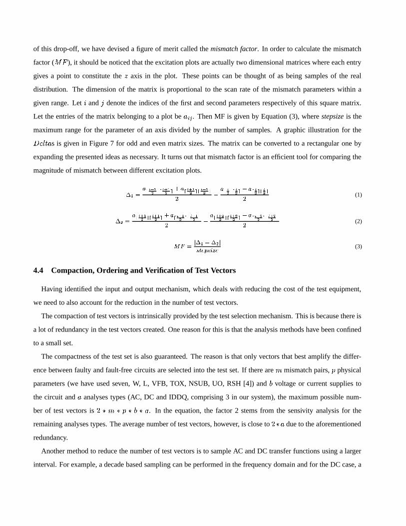
of this drop-off, we have devised a figure of merit called the mismatch factor. In order to calculate the mismatch
factor ( ��� ), it should be noticed that the excitation plots are actually two dimensional matrices where each entry
gives a point to constitute the � axis in the plot. These points can be thought of as being samples of the real
distribution. The dimension of the matrix is proportional to the scan rate of the mismatch parameters within a
given range. Let � and � denote the indices of the first and second parameters respectively of this square matrix.
Let the entries of the matrix belonging to a plot be ��� . Then MF is given by Equation (3), where stepsize is the
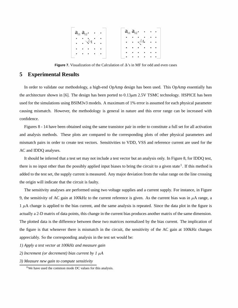
maximum range for the parameter of an axis divided by the number of samples. A graphic illustration for the� ����� � s is given in Figure 7 for odd and even matrix sizes. The matrix can be converted to a rectangular one by
expanding the presented ideas as necessary. It turns out that mismatch factor is an efficient tool for comparing the
magnitude of mismatch between different excitation plots.
������������� �!#"%$ ��� �!'&�( � $ �)�*�!#& �+��� �!'", - � � �!."%$ �!/& ( � $ �!/& � �!/", (1)
�102� ��� ��� �!'"%$ ��� �!'&3( � $ ��� �!'& � ��� �!'", - �4� �)� !!'"%$ �)� !!'&3( � $ �)� !!'& � �)� !!'", (2)
576 �98 �:� - � 0 8;=<?>?@A;CBEDF> (3)
4.4 Compaction, Ordering and Verification of Test Vectors
Having identified the input and output mechanism, which deals with reducing the cost of the test equipment,
we need to also account for the reduction in the number of test vectors.
The compaction of test vectors is intrinsically provided by the test selection mechanism. This is because there is
a lot of redundancy in the test vectors created. One reason for this is that the analysis methods have been confined
to a small set.
The compactness of the test set is also guaranteed. The reason is that only vectors that best amplify the differ-
ence between faulty and fault-free circuits are selected into the test set. If there are G mismatch pairs, H physical
parameters (we have used seven, W, L, VFB, TOX, NSUB, UO, RSH [4]) and I voltage or current supplies to
the circuit and � analyses types (AC, DC and IDDQ, comprising 3 in our system), the maximum possible num-
ber of test vectors is
�J G J H J I J � . In the equation, the factor 2 stems from the sensivity analysis for the
remaining analyses types. The average number of test vectors, however, is close to
�J � due to the aforementioned
redundancy.
Another method to reduce the number of test vectors is to sample AC and DC transfer functions using a larger
interval. For example, a decade based sampling can be performed in the frequency domain and for the DC case, a
Remaining
Physical ParametersCompleted?
no
Done
Mismatch Pairs and
no
no
Run Current Analysis
Add Current Method to Test Set
Compare Method w/ Previous Methods
(V,T) pairs andRemaining
no
Completed?
Larger than All?
Analysis Points
Compare w/ Stored Mismatch Factors
Calculate Mismatch Factor
Store Mismatch Factor
Reset Stored Mismatch Factors
Different from All by a limit?
Figure 6. Test Generation and Compaction Algorithm
smaller range can be scanned with equal intervals. When applied, these methods lead to more compact test sets,
as test vectors falling into a close proximity of a similar test vector, say at a very close frequency, will essentially
have been mapped to the same frequency, eliminating one of the vectors from the set without any fault coverage
loss.
This test set should be applied before any functional test vectors for a circuit, as this set will potentially catch
more faults then a pure functional test set.
Another important point of the proposed methodology is the verification of test vectors. Analog test vector
verification is similarly time consuming and can be costly if tried at the silicon level directly. As the proposed
vectors are generated using simulation results, the vectors need no further verification.
aa11 12
1
aa11 12
1
Figure 7. Visualization of the Calculation of � ’s in MF for odd and even cases
5 Experimental Results
In order to validate our methodology, a high-end OpAmp design has been used. This OpAmp essentially has
the architecture shown in [6]. The design has been ported to 0.13 � m 2.5V TSMC technology. HSPICE has been
used for the simulations using BSIM3v3 models. A maximum of 1% error is assumed for each physical parameter
causing mismatch. However, the methodology is general in nature and this error range can be increased with
confidence.
Figures 8 - 14 have been obtained using the same transistor pair in order to constitute a full set for all activation
and analysis methods. These plots are compared to the corresponding plots of other physical parameters and
mismatch pairs in order to create test vectors. Sensitivities to VDD, VSS and reference current are used for the
AC and IDDQ analyses.
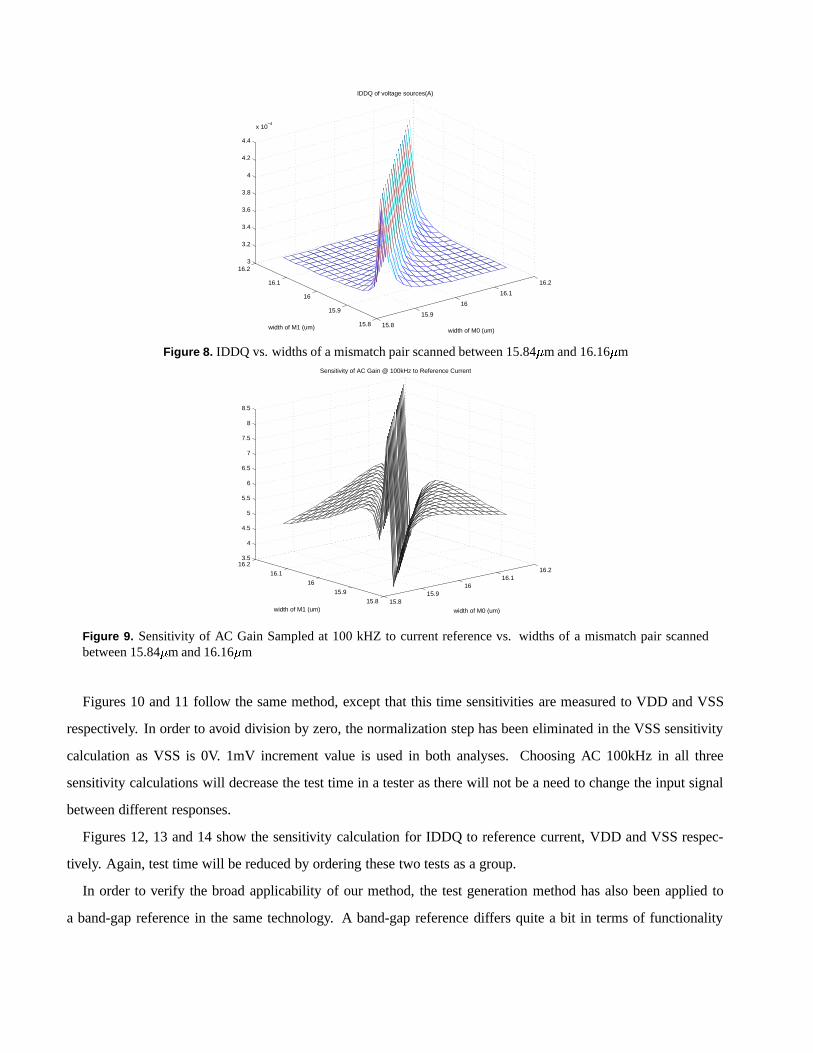
It should be inferred that a test set may not include a test vector but an analysis only. In Figure 8, for IDDQ test,
there is no input other than the possibly applied input biases to bring the circuit to a given state1. If this method is
added to the test set, the supply current is measured. Any major deviation from the value range on the line crossing
the origin will indicate that the circuit is faulty.
The sensitivity analyses are performed using two voltage supplies and a current supply. For instance, in Figure
9, the sensitivity of AC gain at 100kHz to the current reference is given. As the current bias was in � A range, a
1 � A change is applied to the bias current, and the same analysis is repeated. Since the data plot in the figure is
actually a 2-D matrix of data points, this change in the current bias produces another matrix of the same dimension.
The plotted data is the difference between these two matrices normalized by the bias current. The implication of
the figure is that whenever there is mismatch in the circuit, the sensitivity of the AC gain at 100kHz changes
appreciably. So the corresponding analysis in the test set would be:
1) Apply a test vector at 100kHz and measure gain
2) Increment (or decrement) bias current by 1 � A
3) Measure new gain to compute sensitivity�We have used the common mode DC values for this analysis.
15.8
15.9
16
16.1
16.2
15.8
15.9
16
16.1
16.23
3.2
3.4
3.6
3.8
4
4.2
4.4
x 10−4
width of M0 (um)
IDDQ of voltage sources(A)
width of M1 (um)
Figure 8. IDDQ vs. widths of a mismatch pair scanned between 15.84 � m and 16.16 � m
15.815.9
1616.1
16.2
15.8
15.9
16
16.1
16.23.5
4
4.5
5
5.5
6
6.5
7
7.5
8
8.5
width of M0 (um)
Sensitivity of AC Gain @ 100kHz to Reference Current
width of M1 (um)
Figure 9. Sensitivity of AC Gain Sampled at 100 kHZ to current reference vs. widths of a mismatch pair scannedbetween 15.84 � m and 16.16 � m
Figures 10 and 11 follow the same method, except that this time sensitivities are measured to VDD and VSS
respectively. In order to avoid division by zero, the normalization step has been eliminated in the VSS sensitivity
calculation as VSS is 0V. 1mV increment value is used in both analyses. Choosing AC 100kHz in all three
sensitivity calculations will decrease the test time in a tester as there will not be a need to change the input signal
between different responses.
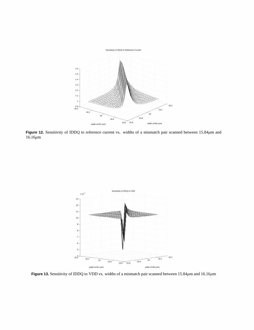
Figures 12, 13 and 14 show the sensitivity calculation for IDDQ to reference current, VDD and VSS respec-
tively. Again, test time will be reduced by ordering these two tests as a group.
In order to verify the broad applicability of our method, the test generation method has also been applied to
a band-gap reference in the same technology. A band-gap reference differs quite a bit in terms of functionality

15.8
15.9
16
16.1
16.2
15.8
15.9
16
16.1
16.2−10
−8
−6
−4
−2
0
width of M0 (um)
Sensitivity of AC Gain @ 100kHz to VDD
width of M1 (um)
Figure 10. Sensitivity of AC Gain Sampled at 100 kHZ to VDD vs. widths of a mismatch pair scanned between15.84 � m and 16.16 � m
from an OpAmp. Band-gap reference is used in order to stabilize the output voltage or current to compensate
for any process and temperature variations. There is no explicit input to the circuit, hence no transfer function
is present. However, our TOM methodology also proposes alternate means of testing the circuit other than using
test vectors. With a small modification to the analysis method, the output voltage of the bandgap reference can be
used directly, instead of the transfer function. Also, IDDQ test is applicable as well as sensitivities of these two
analyses methods to VDD and VSS.
Not all mismatch pairs have equivalent importance on the performance of a circuit, however. Some pairs are
observed to effect the circuit performance so gradually that mismatch amplification methods are not able to amplify
the effects to the point that they can be observed visually. These cases, however, can be handled by assigning a
range to the specified test results. This range should define the useful circuit performance. A range is not needed
for more important mismatch pairs, which are usually much larger in number, as they can be easily identified by
observing the outputs.
6 Summary and Conclusion
The importance of a specialized test for mismatch is very high. A low-cost, general and deterministic method-
ology to test circuits for the presence of mismatch has been necessary. This paper brings forth a methodology to
accomplish this using the notion of mismatch amplification. The proper choice of the members of the test set for
TOM is given using two high-end circuits as examples. The compaction, ordering and verification of test vectors
are additionally discussed in the light of the presented method. The TOM methodology distinguishes between

15.815.9
1616.1
16.2
15.815.9
1616.1
16.20.2
0.25
0.3
0.35
0.4
0.45
0.5
0.55
0.6
0.65
width of M0 (um)
Sensitivity of AC Gain @ 100kHz to Ref. Current
width of M1 (um)
Figure 11. Sensitivity of AC Gain Sampled at 100 kHZ to VSS vs. widths of a mismatch pair scanned between 15.84 � mand 16.16 � m
design and test, is deterministic and self-adequate. The introduced methodology will help speed up analog design
to prevent it becoming the limiting factor in mixed-signal design flows.
References
[1] F. J. Ferguson and J. P. Shen, “A CMOS Fault Extractor for Inductive Fault Analysis,” IEEE Transactions on CAD of IntegratedCircuits and Systems, Vol. 7, No. 11, pp. 1181-1194, Nov. 1988.
[2] M. Slamani and B. Kaminska, “Analog Circuit Fault Diagnosis Based on Sensitivity Computation and Functional Testing,” IEEEDesign and Test of Computers, Vol. 9, No. 1, pp. 30-39, Mar. 1992.
[3] L. Milor and A. Sangiovanni-Vincentelli, “Optimal Test Set Design for Analog Circuits,” IEEE ICCAD, pp 294-297, Nov. 1990
[4] P. G. Drennan and C. C. McAndrew, “A Comprehensive MOSFET Mismatch Model,” IEDM, pp. 167-170, Dec. 1999
[5] R. Sarpeshkar, J. L. Wyatt Jr., N. C. Lu and P. D. Gerber, “Mismatch Sensitivity of a Simultaneously Latched CMOS Sense Amplifier,”IEEE JSSC, Vol. 26, No. 10, pp.1413-1422, Oct. 1991
[6] R. Hogervorst, J. Tero, R. Eschauzier and J. Huijsing, “A Compact Power-Efficient 3 V CMOS Rail-to-Rail Input/Output OperationalAmplifier for VLSI Cell Libraries,” JSSC, Vol. 29, No. 12, pp. 1505-1513, Dec. 1994
[7] M. Jarwala and S. J. Tsai, “A Framework for Design for Testability of Mixed Analog/Digital Circuits,” IEEE CICC, pp. 13.5/1-13.5/4,May. 1991
[8] L. S. Prabhu and D.A. Rosenthal, ”A DSP-Based Feedback Loop for Mixed-Signal VLSI Testing” Proceedings of ITS, pp. 670-674,Nov. 1997
[9] S. Ozev and A. Orailoglu, ”Boosting the Accuracy of Analog Test Coverage Computation through Statistical Tolerance Analysis”Proceedings of the 20th IEEE VTS, pp.213-219, May. 2002
[10] K. Arabi and B. Kaminska, ”Oscillation Test Strategy for Analog and Mixed-Signal Integrated Circuits” Proceedings of the 14thIEEE VTS, pp. 476-482, May. 1996
15.8
15.9
16
16.1
16.2
15.8
15.9
16
16.1
16.20.9
1
1.1
1.2
1.3
1.4
1.5
1.6
width of M0 (um)
Sensitivity of IDDQ to Reference Current
width of M1 (um)
Figure 12. Sensitivity of IDDQ to reference current vs. widths of a mismatch pair scanned between 15.84 � m and16.16 � m
15.815.9
1616.1
16.2
15.815.9
1616.1
16.24
5
6
7
8
9
10
11
12
13
x 10−4
width of M0 (um)
Sensitivity of IDDQ to VDD
width of M1 (um)
Figure 13. Sensitivity of IDDQ to VDD vs. widths of a mismatch pair scanned between 15.84 � m and 16.16 � m

15.815.9
1616.1
16.2
15.815.9
1616.1
16.2−1.2
−1
−0.8
−0.6
−0.4
−0.2
0
x 10−3
width of M0 (um)
Sensitivity of IDDQ to VSS
width of M1 (um)
Figure 14. Sensitivity of IDDQ to VSS vs. widths of a mismatch pair scanned between 15.84 � m and 16.16 � m