
TESIS DOCTORAL Study of ferroelectric PbTiO...
202
UNIVERSIDAD CARLOS III DE MADRID Instituto de Química y Materiales Álvaro Alonso Barba TESIS DOCTORAL Study of ferroelectric PbTiO 3 nanostructures deposited onto substrates and prepared by a novel microemulsion mediated synthesis Autor: María Torres Sancho Directoras: Dra. Mª Lourdes Calzada Coco Prof. Lorena Pardo Mata Consejo Superior de Investigaciones Científicas Instituto de Ciencia de Materiales de Madrid Leganés, noviembre de 2009
Transcript of TESIS DOCTORAL Study of ferroelectric PbTiO...

UNIVERSIDAD CARLOS III DE MADRID
Instituto de Química y Materiales Álvaro Alonso Barba
TESIS DOCTORAL
Study of ferroelectric PbTiO3
nanostructures deposited onto substrates
and prepared by a novel microemulsion
mediated synthesis
Autor:
María Torres Sancho
Directoras:
Dra. Mª Lourdes Calzada Coco
Prof. Lorena Pardo Mata
Consejo Superior de Investigaciones Científicas
Instituto de Ciencia de Materiales de Madrid
Leganés, noviembre de 2009
TESIS DOCTORAL
Study of ferroelectric PbTiO3 nanostructures deposited onto
substrates and prepared by a novel microemulsion mediated
synthesis
Autor: María Torres Sancho
Directoras: Dra. Mª Lourdes Calzada Coco
Prof. Lorena Pardo Mata
Firma del Tribunal Calificador:
Firma Presidente:
Vocal:
Vocal:
Vocal:
Secretario:
Calificación:
Leganés, de noviembre de 2009


A Dani


Esta Tesis Doctoral se ha realizado en el Departamento de Materiales para la Tecnología de la
Información del Instituto de Ciencia de Materiales de Madrid (ICMM-CSIC), bajo la dirección de la
Dra. Mª Lourdes Calzada Coco y la Prof. Lorena Pardo Mata, gracias a la concesión de una beca del
Programa de Formación de Personal Investigador (FPI) del Ministerio de Ciencia y Tecnología,
asociada al proyecto de investigación “Procesado por sol-gel de materiales nanométricos y
nanocaracterización piezoeléctrica para ferroeléctricos integrados” (MAT2004-02014). Además,
parte de este trabajo ha sido parte de las COST action 539-ELENA y de la EC network of excellence
on Multifunctional and Integrated Piezoelectric Devices NoE 515757.
Muchas son las personas que, directa o indirectamente, me han ayudado a desarrollar este trabajo
y es justo comenzar la redacción de esta tesis agradeciéndoselo.
En primer lugar, me gustaría agradecer a la Dra. Mª Lourdes Calzada Coco y la Prof. Lorena Pardo
Mata su dedicación, esfuerza y ayuda durante todo el tiempo que ha durado esta tesis. Por su
búsqueda constante de la excelencia, por su confianza en mí desde el principio y por enseñarme
tantas cosas, científicas y no científicas.
Al Dr. Jesús Ricote, por su infinita paciencia con mis dudas sobre microscopía de fuerza y por su
gran capacidad didáctica, de la que tanto he aprendido.
A los Dres. Ricardo Jiménez, Miguel Algueró, Harvey Amorín y Pablo Ramos, por interesarse
siempre por la evolución de la tesis y por sus palabras de ánimo.
Al Dr. Iñigo Bretos, por su ayuda en mis primeros y titubeantes días y su apoyo en estos últimos.
A los Dres. Miguel Ángel Martínez y Alejandro Várez, por su ayuda con los trámites necesarios para
presentar esta tesis al comienzo y al final del proceso.
I would like to thank Dr. Zhaorong Huan y Dr. Sue Impey, for accepting me in their group at
Cranfield University from November 18th to December 2nd of 2006, within the frame of the COST
action 539-ELENA. Many thanks for their help and contribution to this work, particularly to
Christine Kimpton for part of the SEM images.
Al Dr. Fuentes Cobas, por aceptarme a mí y a mis muestras en aquel viaje a Stanford. Gracias a ésa y
a sucesivas expediciones científicas, se pudieron analizar las nanoestructuras preparadas en este
trabajo mediante radiación sincrotrón. Al Dr. Fuentes Montero, por permitirme utilizar esa joya de

programa que es ANAELU: Gracias a ambos por las noches de discusión científica sobre
interpretación de resultados. Special acknowledge is due to Dr. Apurva Mehta and the Stanford
Synchrotron Radiation Lightsource for the diffraction measurements and fruitful discussion.
I would like to thank Dr. Marin Alexe, for accepting me in his group at the Max Planck Institute of
Microstructure Physics at Halle, from May 5th to August 11th 2008, within the framework of a short-
term stay in a foreign laboratory granted by the FPI program. Many thanks for so many interesting
talks about PFM, ferroelectricity and scientific life. I would like to acknowledge Dr. Brian Rodriguez
for his help, teaching and valuable discussion about PFM. I would like to thank both for the warm
care they bestowed on me during my stay. I would also like to thank the entire group for making my
stay a pleasure.
A la Dra. María Alonso del Departamento de Nanoestructuras y Superficies del Instituto de Ciencia
de Materiales de Madrid, por realizar las medidas de espectroscopía de electrones Auger y de
difracción de electrones de baja energía, por su ayuda a la hora de interpretar los resultados, así
como por sus valiosas sugerencias sobre la versión final de la discusión de dichos resultados en este
manuscrito.
Al Dr. Pedro Tartaj del Departamento Biomateriales y Materiales Bioinspirados del Instituto de
Ciencia de Materiales de Madrid,por realizar las medidas de Dynamic Light Scattering y por su
ayuda a la hora de interpretar los resultados.
A la Dra. Lidia Martínez, por realizar las medidas de ángulo de contacto y por su ayuda a la hora de
interpretar los resultados.
Al equipo de Nanotec Electrónica, por su ayuda. Especialmente, a Luís Colchero, por su paciencia,
su disponibilidad y por las muchas cosas que me ha enseñado sobre microscopía de fuerzas.
Gracias también a los Dres. Alfredo Álvarez y Pilar Suárez, con quienes empecé esta etapa de mi
vida. Gracias por darme la primera oportunidad y avivar el gusanillo de la Ciencia.
Gracias a Elvira, Lidia y Renaud, por enseñarme a afrontar los problemas con optimismo y a
relativizarlos. A Mercedes, por preocuparse siempre por mí y mi tesis. A Carlos (Carlitos), Ana, César
y Ramón, por su simpatía y por hacer de los momentos de asueto del día un momento divertido.
A Álvaro, por su paciencia con mis múltiples formateos del disco duro del ordenador y por las risas,
tan necesarias en el periodo de escritura. A los que se fueron (Alfonso, Abel y Raquel) y los que
llegaron (David y Hidham).

De todo corazón, a mis amigas María, Aurora e Irene, por perdonarme el haberme perdido
momentos muy importantes (como Pablete) y acompañarme en todas las grandes encrucijadas que
han ido llegando. Porque hemos ido creciendo juntas y siempre nos hemos apoyado.
Tengo que agradecer a mi familia por apoyar mis decisiones personales y profesionales, por estar a
mi lado pase lo que pase. Gracias por inculcarme el tesón, el perfeccionismo en su justa medida y la
eficiencia.
Y no puedo acabar sin agradecer a Dani su apoyo durante todo este periodo. Por hacerme
compañía con su presencia en las noches de escritura, por tenerme siempre la cena calentita con
una sonrisa. Por esperarme después de cada viaje, por entender que la investigación es mi vida y lo
que me hace feliz y no intentar cambiarlo. Por entender que comprometerse conmigo era también
hacerlo con esta tesis. Porque sin ti, Dani, esta tesis hubiera sido mucho más dura y ni la mitad de
divertida. Gracias.

Resumen:
Los materiales ferroeléctricos presentan una serie de propiedades que les hace
apropiados para un gran número de aplicaciones. Estos materiales presentan dos
estados de polarización de igual energía entre los que se puede transitar mediante la
aplicación de un campo eléctrico externo, convirtiéndolos en materiales muy
atractivos para su utilización en memorias RAM. Hoy en día, la tendencia de los
dispositivos de memoria es aumentar la densidad de almacenamiento, que se
encuentra actualmente en los Tb/inch2, manteniendo o disminuyendo su coste. Para
ello, es imprescindible poder fabricar unidades de almacenamiento cada vez más
pequeñas, manteniendo sus propiedades y a un coste lo más bajo posible.
En la presente tesis doctoral se ha desarrollado un método novedoso de procesado
basado en la tecnología “bottom-up” para la obtención de nanoestructuras
ferroeléctricas de PbTiO3 sobre sustratos para su uso en memorias no volátiles, NV-
FeRAMs. Este procedimiento implica el depósito sobre substratos de las disoluciones
micelares resultantes de la mezcla de soles y microemulsiones mediante la técnica de
Depósito Químico de Disoluciones (CSD).
Para comparar los resultados que se obtendrán en el transcurso de esta tesis, se han
preparado nanoestructuras explotando el fenómeno de la inestabilidad estructural de
láminas ultradelgadas. Según este fenómeno, cuando el espesor de éstas es menor de
un valor crítico, la película se rompe, dando lugar a estructuras aisladas. Se
prepararon diferentes muestras, analizando el fenómeno antes y después de este
espesor crítico, obteniéndose nanoestructuras aisladas con un límite inferior de
tamaño lateral ~50 nm. Al analizar los depósitos, no se aprecia orden sobre el
substrato. Mediante difracción de rayos-X de radiación sincrotrón en ángulo rasante,
se ha determinado la orientación de las nanoestructuras, siendo ésta de fibra y
presentando un cono de distribución direcciones de ±15°. Mediante microscopía de
fuerzas en modo piezorespuesta (PFM), se ha comprobado el carácter ferro-
piezoeléctrico a escala local de estas partículas.
En esta tesis, se ha desarrollado una novedosa tecnología de procesado para la
obtención de nanoestructuras ferroeléctricas de PbTiO3, basada en el depósito de
soluciones micelares resultantes de la mezcla de soles y microemulsiones, y en la
funcionalización de la superficie de los substratos. Se hipotetiza que las micelas
formarán una red organizada una vez depositadas sobre el sustrato, de forma que el
depósito de la disolución micelar dará lugar a una disposición ordenada sobre la
superficie del sustrato de las nanoestructuras y que, además, tendrán un tamaño y
forma controladas. Las micelas proporcionan un entorno aislado a las partículas de sol
que se encuentran en su interior, pudiendo producirse las reacciones químicas de
síntesis de los componentes. Esta característica de las micelas, sumada a su capacidad
de auto ordenación, hace de ellas las “building units” o elementos primarios para las
nanoestructuras ferroeléctricas de PbTiO3. Utilizando este método, se prepararon
nanoestructuras sobre sustratos policristalinos de Pt-(100)Si, compatibles con la
tecnología actual del silicio, y sobre sustratos monocristalinos de SrTiO3.
Sobre los sustratos policristalinos de Pt-(100)Si, se obtuvieron nanoestructuras con un

tamaño promedio de ~70 nm y con una morfología semejante a partir de disoluciones
con diferentes concentración. Estas nanoestructuras son el resultado de la
coalescencia entre un número finito de nanoestructuras primarias. Al analizar las
distribuciones de tamaños de las partículas obtenidas, se deduce que éstas crecen de
forma independiente. Esto contrasta con las nanoestructuras obtenidas mediante
inestabilidad microestructural, que siguen un mecanismo de nucleación y difusión
entre las nanoestructuras vecinas. Esta diferencia confirma la hipótesis de que las
micelas actúan de “building units” de estas nanoestructuras. Sin embargo, las
nanoestructuras preparadas mediante este procedimiento sobre los sustratos
policristalinos no se disponen ordenadamente sobre éte, debido fundamentalmente a
los defectos de la superficie del substrato. Para mejorar la calidad de esta superficie
sobre la que se hace el depósito, ésta se funcionalizó, de forma que se modificó con el
depósito previo de una película de microemulsión. Al depositar la solución micelar
sobre esta superficie funcionalizada, se obtuvieron, después de la cristalización,
nanoestructuras agregadas, como en el caso anterior, y nanoestructuras primarias,
que presentan un tamaño promedio de ~21 nm y con una disposición hexagonal sobre
el sustrato, orden de corto alcance. Las nanoestructuras presentan la estructura
cristalina de la perovskita de PbTiO3 con estructura de fibra y dos de cuyos ejes
presentan un cono de direcciones probables de ±20°, como se determinó mediante
difracción de rayos-X de radiación sincrotrón en ángulo rasante. Las medidas de PFM
confirmaron el carácter ferro-piezoeléctrico de las nanoestructuras, midiéndose en la
nanoestructura más pequeña hasta el momento, ~37 nm y altura de ~14 nm. Según
conocimiento de la autora, este tamaño de nanoestructura aislada está por debajo de
los publicados en la literatura para los que se han obtenido respuesta ferroeléctrica.
Con el objetivo de utilizar substratos con superficies más próximas a la ideal que los
policristalinos utilizados anteriormente, se utilizaron substratos monocristalinos de
SrTiO3. De esta manera, tras probar la validez del método del depósito de soluciones
micelares para la obtención de nanoestructuras primarias de tamaño y forma
controladas y con una disposición ordenada sobre el sustrato, se pretendió mejorar la
disposición ordenada de estas nanoestructuras sobre el substrato. Sin embargo, el
mojado del substrato por la disolución micelar fue muy deficiente, lo que conllevó un
recubrimiento no uniforme del substrato monocristalino. Éste comportamiento se
utilizó para determinar el tipo de crecimiento y de orden de las nanoestructuras de
PbTiO3 sobre los sustratos de SrTiO3. Se determinó que el crecimiento era de tipo
Frank-van der Merwe. Los experimentos de difracción de rayos-X de radiación
sincrotrón en ángulo rasante confirmaron la estructura perovskita del PbTiO3, así
como el crecimiento epitaxial sobre el sustrato. Mediante PFM se midió la respuesta
ferro-piezoeléctrica de las nanostructuras.
Por último, para subsanar los defectos del mojado del sustrato de SrTiO3 por la
solución micelar, se funcionalizó la superficie mediante un tratamiento químico y
térmico, de forma que al depositar la solución micelar sobre el sustrato de SrTiO3 tras
modificar su superficie, se observó la uniformidad del recubrimiento en todo el
substrato y un orden a largo alcance de las nanoestructuras de PbTiO3.

Abstract:
Ferroelectric materials present some properties that make them suitable for a large
number of applications. This materials present to states of polarization of equal
energy, switchable by an external electric field. This makes of them a very attractive
material for their use as random access memories (RAM). Nowadays, the trend in
memory devices is to increase the storage density, which is actually in the Tb/inch2,
maintaining or decreasing the fabrication cost. To achieve that, it is mandatory to be
able to fabricate smaller storage units that keep their properties and at the lowest
cost.
In this thesis, a novel processing method based in the “bottom-up” technology is
developed for the fabrication of ferroelectric PbTiO3 nanostructures onto substrates
for their use, for example, as non volatile ferroelectric RAM, NV-FeRAMs. This
procedure implies the deposition onto substrates of micellar solutions, resulting of
the mixture of sols and microemulsions by the Chemical Solution Deposition
technique (CSD).
In order to compare the results obtained in this thesis, nanostructures had been
prepared using the phenomenon of the microstructural instability of ultrathin films.
According to this phenomenon, when the thickness of an ultrathin film is below a
critical one, it breaks, yielding isolated nanostructures. Different samples were
prepared, studying the phenomenon before and after the critical thickness and
obtaining isolated nanostructures of ~50 nm of lateral size. Self-assembly of the
nanostructures onto the substrate was not observed. By synchrotron X-ray diffraction
in grazing incidence, it was possible to determine the texture of the nanostructures: it
is a fiber texture with an orientation distribution cone of ±15°. By Piezoresponse Force
Microscopy (PFM), the ferro-piezoelectric character of the nanostructures at a local
scale was proved.
In this thesis, it is proposed a novel processing technology for the fabrication of
ferroelectric PbTiO3 nanostructures, based in the deposition of micellar solutions
resulting from the mixture of sols and microemulsions and in the functionalization of
the substrates. Micelles are hypothesized to form a self-assembly network, once
deposited onto the substrate, so that the deposit of the micellar solution will rise to a
self-assembly onto the surface of the substrate with controlled size and shape. In
addition, micelles provide an isolated environment for the sol particles in their inside,
and the chemical reactions of synthesis of the components might occur. These
properties of the micelles, makes of them the “building units” for the ferroelectric
PbTiO3 nanostructures. By using this method, nanostructures were prepared onto
polycrystalline Pt-(100)Si substrates, compatible with the actual Si technology, and
onto single crystal SrTiO3 substrates.
Nanostructures were obtained onto the polycrystalline Pt-(100)Si substrates with an
average size of ~70 nm and with a similar morphology from solutions of different
concentration. These nanostructures are the result of the coalescence of a finite
number of primary nanostructures. From the analysis of the size of the obtained
nanostructures it is deduced that they grow independently, which is contrast with the

growing mechanism of the nanostructures obtained from the phenomenon of the
ultrathin films instability, which mechanism is the nucleation and diffusion between
neighbor nanostructures. This difference confirms the hypothesis of micelles acting as
“building units” of the nanostructures. However, nanostructures prepared by this
procedure onto polycrystalline substrates do not self-assemble onto the substrate,
mainly due to the defects of the surface of the substrate. In order to improve the
quality of this surface, it was functionalized by previously depositing a layer of
microemulsion. When the micellar solution was deposited onto this functionalized
surface, merged nanostructures were obtained after the crystallization process, as
before. Primary nanostructures were also obtained with an average size of ~21 nm
and a hexagonal short-range arrangement onto the substrate. The nanostructures
have the crystalline structure of the PbTiO3 perovskite with a fiber texture and two
axes that present an orientation distribution cone of ±20°, as determined by
synchrotron X-ray diffraction in grazing incidence. PFM measurements confirmed the
ferro-piezoelectric character of the nanostructures, measuring it in nanostructures of
~37 nm of lateral size and ~14 nm of height. To the best of the knowledge of this
author, the size of this isolated nanostructure is below those reported in the literature
where ferroelectric response had been measured.
Single crystal SrTiO3 substrates were used in order to utilize substrates with a surface
closer to the ideal one than the polycrystalline ones used previously. Thus, once the
validity of the microemulsion deposition procedure for the fabrication of primary
nanostructures of controlled size and shape and with a self-assembly onto the surface
of the substrate was proved, an improvement of the self-assembly onto the surface of
the substrates was set as a target. However, the wetting of the substrate by the
micellar solution was deficient, which yield a non-uniform coating of the single crystal
substrate. This behavior was exploited to determine the type of growth and
arrangement of the PbTiO3 nanostructures on the SrTiO3 substrates, establishing that
it is a Frank-van der Merwe growing type. The experiments of synchrotron X-ray
diffraction in grazing incidence configuration confirmed the PbTiO3 perovskite
structure as well as the epitaxial growth onto the substrate. By PFM, the ferro-
piezoelectric response of the nanostructures was measured.
Finally, in order to overcome the deficient wetting of the substrate by the micellar
solution, the surface was functionalized by a chemical and thermal treatment, so that
a uniform coating and a large-range arrangement of the PbTiO3 nanostructures are
observed in the whole substrate, when the micellar solution is deposited onto the
SrTiO3 substrate after modifying the surface.

Table of contents
CHAPTER 1. Introduction
1.1. From ferroelectric bulk ceramics to nanostructures. 1
1.2. State of the art and material requirements in FeRAMs. 3
1.3. State of art of the fabrication of ferroelectric nanostructures onto substrates. 4
1.3.1. The top-down approach. 5
1.3.2. Bottom-up techniques. 6
1.3.3. Hybrid methods. 8
1.4. Ferroelectric compositions of interest for FERAMs. 9
1.4.1. PbTiO3 perovskite structure. 10
1.5. Motivation and purpose of this work. 12
Bibliography 14
CHAPTER 2: Experimental Procedure
2.1. Precursor solutions. 17
2.1.1. Synthesis of the sol. 17
2.1.2.Preparation of the microemulsion. 18
2.1.3. Preparation of the micellar solution. 18
2.2. Selection of substrates.. 19
2.2.1. Pt-coated Si (100) substrates. 19
2.2.2. Microemulsion/Pt- coated Si (100) substrates. 19
2.2.3. (100)SrTiO3 substrates. 19
2.2.4. (100) SrTiO3 substrates with controlled surfaces. 20
2.3. Deposition, drying and crystallization of the PbTiO3 nanostructures. 22
2.4. Microscopy and quantitative microstructure characterization. 23
2.4.1. Optical microscopy. 23
2.4.2. Scanning Electron Microscopy. 23
2.4.3.Transmission Electron Microscopy. 24
2.4.4. Scanning Probe Microscopy. 25
2.4.4.1. Fast Fourier Transform and self-convolution images. 29
2.4.5. Image analyses 30
2.5. Structural characterization. 33
2.5.1. Synchrotron X-ray diffraction. 33
2.5.1.1. Grazing incidence. 35
2.5.2. Auger Electron Spectroscopy. 40
2.5.3. Low Energy Electron Diffraction. 42

Table of contents
2.6. Ferro-piezoelectric characterization: Piezo Response Force Microscopy. 43
2.6.1. Image acquisition. 46
2.6.2. Hysteresis loops. 47
Bibliography 49
CHAPTER 3: Ferroelectric nanostructures by the phenomenon of the microstructural
instability of polycrystalline ultrathin films.
3.1. The microstructural instability of polycrystalline ultrathin films. 53
3.2. Nanoscale PbTiO3 structures onto Pt/TiO2/SiO2/(100)Si substrates prepared by using
the phenomenon of the microstructural instability.
55
3.2.1. Microscopy and quantitative microstructure analysis. 55
3.2.2. Structural characterization. 61
3.2.3. Functional characterization. 66
Remarks. 69
Bibliography 70
CHAPTER 4: Ferroelectric nanostructures by microemulsion mediated synthesis onto
Pt/TiO2/SiO2/(100)Si substrates.
4.1. The microemulsion mediated synthesis 73
4.2. Nanoscale PbTiO3 ferroelectric structures onto Pt/TiO2/SiO2/(100)Si substrates
prepared by microemulsion mediated synthesis.
81
4.2.1. Microscopy and quantitative microstructure analysis. 81
4.2.2. Structural characterization 87
4.2.3. Functional characterization 91
4.3. Nanoscale PbTiO3 ferroelectric structures onto microemulsion
layer/Pt/TiO2/SiO2/(100)Si substrates prepared by the modified microemulsion mediated
synthesis.
98
4.3.1. Microscopy and quantitative microstructure analysis. 102
4.3.2. Structural characterization 112
4.3.3. Functional characterization 117
Remarks 121
Bibliography 123

Table of contents
CHAPTER 5: Nanostructures onto SrTiO3 single-crystal substrates by microemulsion
mediated synthesis
5.1. Towards ideal surfaces 127
5.2. Nanoscale PbTiO3 structures onto commercial as-served SrTiO3 substrates prepared
by microemulsion mediated synthesis.
128
5.2.1. Microscopy analysis. 129
5.2.2. Structural characterization 138
5.2.3. Functional characterization 142
5.3. Nanoscale PbTiO3 structures onto (100)SrTiO3 substrates with controlled surfaces
prepared by microemulsion mediated synthesis.
143
5.3.1 Preparing ideal surfaces: chemical and thermal treatment of the STO surfaces. 145
5.3.2. Microscopy and quantitative microstructure analysis. 156
Remarks 162
Bibliography 164
CHAPTER 6: Conclusions
6.1. Conclusions 167
6.2. Conclusiones 169


List of figures
CHAPTER 1. Introduction
Figure 1.1. Towards the miniaturization of ferroelectric materials and their integration into microelectronic devices.
1
Figure 1.2. Top portion of 512 Mb DDR2 SDRAM stacked capacitors. HSG means hemispherical grain polysilicon.
3
Figure 1.3. Nanostructures and their hysteresis loop prepared by Focused Ion Beam (a) and (b); Nanoimprint Lithography (c) and (d); and Electron Beam Direct Writing (e) and (f).
5
Figure 1.4. Nanostructures prepared by PLD exploiting the Volmer-Webber growing mode (a), using latex microspheres (c) and alumina templates (e) and their corresponding hysteresis loops (b), (d) and (f), respectively. (g) shows nanostructures fabricated exploiting the microstructural instability of ultrathin films and (h) using di-block-copolymers.
7
Figure 1.5. Nanostructures obtained by a hybrid method that combines EBL and CSD (a) and the PFM image that confirms their ferro-piezoelectric character at a local scale (b).
9
Figure 1.6. Interrelationship of piezoelectric and subgroups on the basis of symmetry.
10
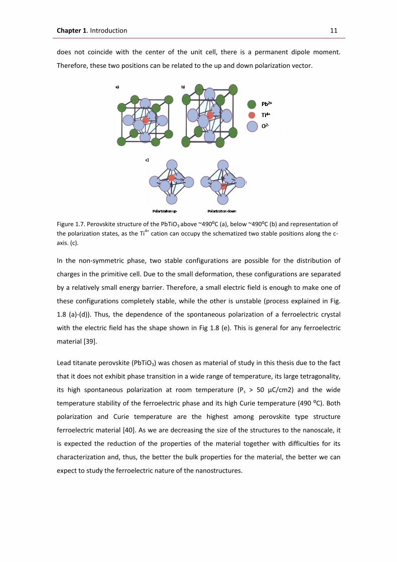
Figure 1.7. Perovskite structure of the PbTiO3 above ~490⁰C (a), below ~490⁰C (b) and representation of the polarization states, as the Ti4+ cation can occupy the schematized two stable positions along the c-axis. (c).
11
Figure 1.8. Mechanical model schematized to explain the existence of dielectric hysteresis in any ferroelectric crystal.
12
CHAPTER 2: Experimental Procedure
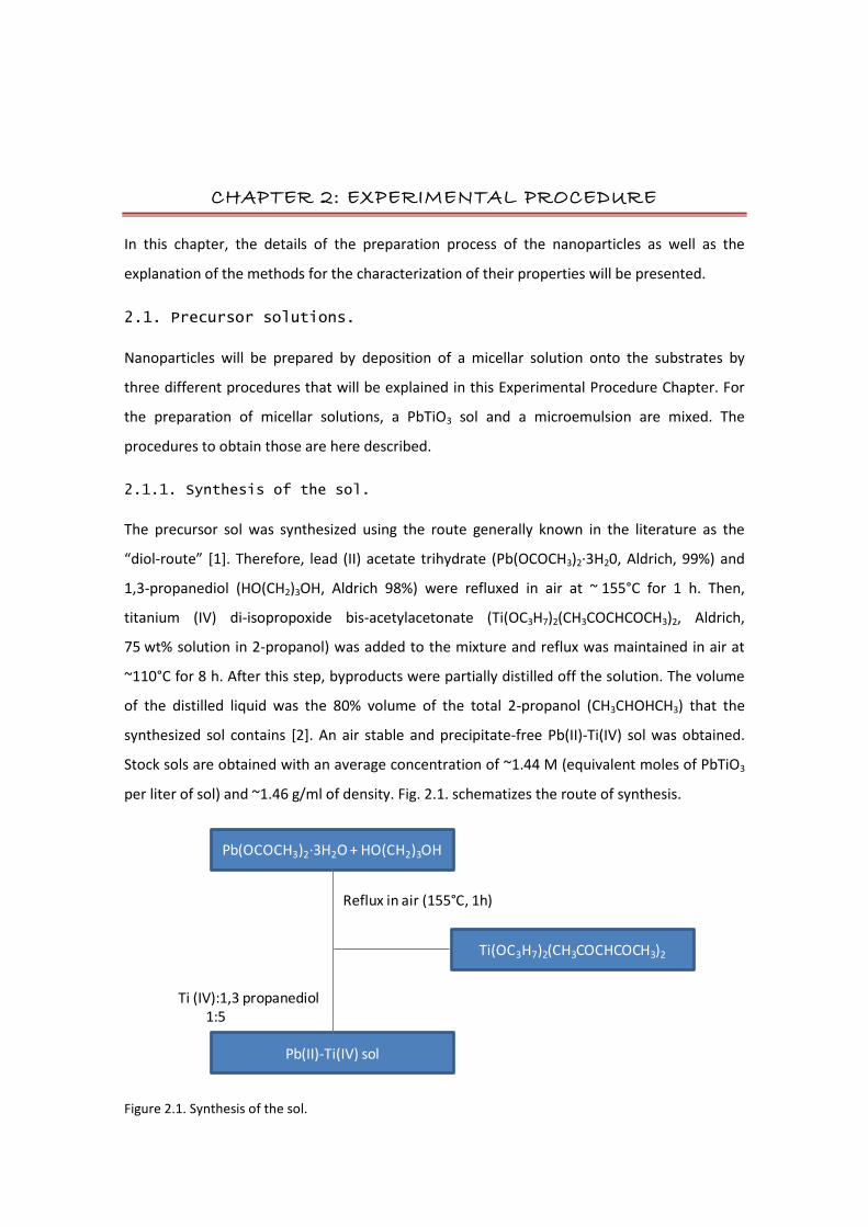
Figure 2.1. Synthesis of the sol.
17
Figure 2.2. Preparation of the microemulsion.
18
Figure 2.3. Preparation of the micellar solution.
18
Figure 2.4. Thermal treatments in UHV applied to the STO substrates.
20
Figure 2.5. RTP thermal treatments applied to the STO substrates.
21
Figure 2.6. Spin-coating process.
22
Figure 2.7. Thermal recipe used for the crystallization of the nanostructures.
23
Figure 2.8. Experimental set-up of a SPM system.
26
Figure 2.9. Force-distance curve of the interaction between the probe tip and the sample surface.
26
Figure 2.10. Artifacts of the AFM topography image in contact mode in the case of tip radius smaller (a) and larger (b) than the measured nanostructures.
27
List of figures
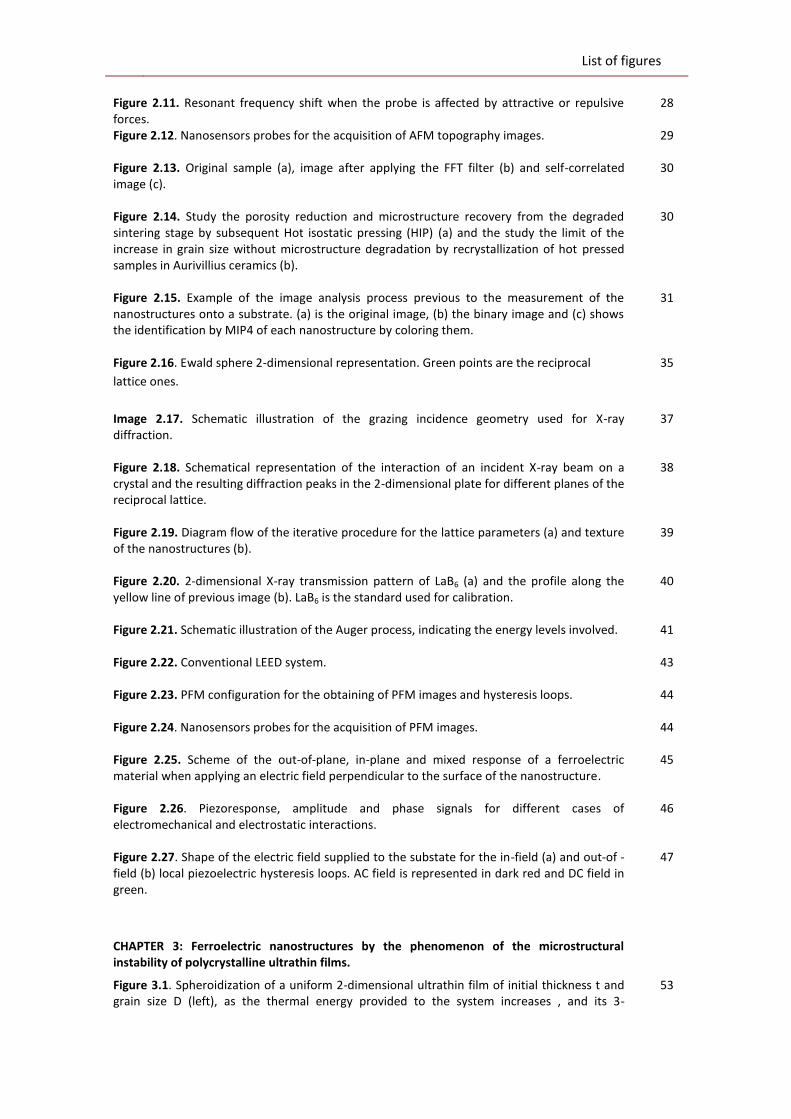
Figure 2.11. Resonant frequency shift when the probe is affected by attractive or repulsive forces.
28
Figure 2.12. Nanosensors probes for the acquisition of AFM topography images.
29
Figure 2.13. Original sample (a), image after applying the FFT filter (b) and self-correlated image (c).
30
Figure 2.14. Study the porosity reduction and microstructure recovery from the degraded sintering stage by subsequent Hot isostatic pressing (HIP) (a) and the study the limit of the increase in grain size without microstructure degradation by recrystallization of hot pressed samples in Aurivillius ceramics (b).
30
Figure 2.15. Example of the image analysis process previous to the measurement of the nanostructures onto a substrate. (a) is the original image, (b) the binary image and (c) shows the identification by MIP4 of each nanostructure by coloring them.
31
Figure 2.16. Ewald sphere 2-dimensional representation. Green points are the reciprocal
lattice ones.
35
Image 2.17. Schematic illustration of the grazing incidence geometry used for X-ray diffraction.
37
Figure 2.18. Schematical representation of the interaction of an incident X-ray beam on a crystal and the resulting diffraction peaks in the 2-dimensional plate for different planes of the reciprocal lattice.
38
Figure 2.19. Diagram flow of the iterative procedure for the lattice parameters (a) and texture of the nanostructures (b).
39
Figure 2.20. 2-dimensional X-ray transmission pattern of LaB6 (a) and the profile along the yellow line of previous image (b). LaB6 is the standard used for calibration.
40
Figure 2.21. Schematic illustration of the Auger process, indicating the energy levels involved.
41
Figure 2.22. Conventional LEED system.
43
Figure 2.23. PFM configuration for the obtaining of PFM images and hysteresis loops.
44
Figure 2.24. Nanosensors probes for the acquisition of PFM images.
44
Figure 2.25. Scheme of the out-of-plane, in-plane and mixed response of a ferroelectric material when applying an electric field perpendicular to the surface of the nanostructure.
45
Figure 2.26. Piezoresponse, amplitude and phase signals for different cases of electromechanical and electrostatic interactions.
46
Figure 2.27. Shape of the electric field supplied to the substate for the in-field (a) and out-of -field (b) local piezoelectric hysteresis loops. AC field is represented in dark red and DC field in green.
47
CHAPTER 3: Ferroelectric nanostructures by the phenomenon of the microstructural instability of polycrystalline ultrathin films.
Figure 3.1. Spheroidization of a uniform 2-dimensional ultrathin film of initial thickness t and grain size D (left), as the thermal energy provided to the system increases , and its 3-
53

List of figures
dimensional analysis (right) Figure 3.2. Nanoparticles of Pb(Ti, Zr)O3 (PZT) onto SrTiO3 volume distribution.
54
Figure 3.3. AFM topography images of a PbTiO3 continuous ultrathin film obtained at different magnifications: 5x5 µm image (a) and 2x2 µm image (b).
56
Figure 3.4 AFM topography images and representative profiles of the PbTiO3 nanostructures onto the Pt/TiO2/SiO2/(100)Si substrates prepared from sols with different concentrations.
57
Figure 3.5. Proposed growth evolution of the particles deposited as the concentration of the solutions decreases.
58
Figure 3.6. Equivalent diameter distributions of samples prepared from the 4·10-2
M (a) and 3·10
-2 M (b) sol-gel solutions and their corresponding log-normal distributions (c) and (d).
60
Figure 3.7. Experimental 2-D Synchrotron diffraction pattern of a continuous ultrathin film.
62
Figure 3.8 2θ diffraction pattern obtained from the integration of the 2-D experimental
pattern and the simulated diffraction patterns of the PbTiO3, platinum, TiO2 and silicon of the
substrate.
63
Figure 3.9. Simulated 2-D diffraction pattern of polycrystalline platinum with (111) fiber texture (a) and the experimental 2-D diffraction pattern measured from the ultrathin film (b).
64
Figure 3.10. Simulated 2-D diffraction pattern of (100) Si single crystal (a) and the measured 2-D diffraction pattern from the sample (b). The diffractions maxima that forms the triangle are marked with a cross.
64
Figure 3.11. Simulated 2-D diffraction pattern of PbTiO3 nanostructures with (100) fiber
texture and an orientation distribution cone of ±15° (a) and the measured 2-D diffraction
pattern from the sample (b).
65
Figure 3.12. Topography (a) and (d), phase (b) and amplitude (c) images of the in-plane piezoresponse and phase (e) and amplitude (f) of the out-of-plane piezoresponse for the continuous ultrathin PbTiO3 film.
67
Figure 3.13. Topography (a), phase (b) and amplitude (c) images of the out-of-plane piezoresponse for the PbTiO3 nanostructures.
67
Figure 3.14. Out-of-field consecutive local hysteresis loops of a nanoparticle of 50nm.
68
Figure 3.15. Scheme of the pinned layer and the imprint (a) and its effect on a hysteresis loop (b).
68
CHAPTER 4: Ferroelectric nanostructures by microemulsion mediated synthesis onto Pt/TiO2/SiO2/(100)Si substrates.
Figure 4.1. Representation of Brij-30 with the head and tail groups indicated.
73
Figure 4.2. Some of the possible colloidal aggregates of surfactant molecules in an emulsion.
74
Figure 4.3. Schema of the inverse micelles inside the microemulsion prepared in this work.
75

List of figures
Figure 4.4. Schematic formation process of the micellar solution. 76
Figure 4.5. Hypothetical self-assembly of the nanostructures.
78
Figure 4.6. Tyndall effect in the microemulsion (a), sol (b) and micellar solution (c).
79
Figure 4.7. DLS measurements for the microemulsion (a), sol (b) and micellar solution (c).
80
Figure 4.8. Topography by optical microscopy of the limit of the coating area (a) and SEM micrograph of the center of the non-homogenous coating (b) (sample prepared from a 5·10
-
3 M micellar solution).
82
Fig. 4. 9. AFM topography images of the PbTiO3 nanostructures onto Pt/TiO2/SiO2/(100)Si substrates prepared from the micellar solutions with a sol concentration of 10
-2 M (a-b) and
5·10-3
M (c) at different locations of the coated substrate.
83
Figure 4.10. High magnification AFM image of isolated nanostructures fabricated from the 5·10
-3 M micellar solution.
84
Figure 4.11. Proposed drying evolution with time of the micellar layer (a, b) and oxide nanostructures formed after the thermal treatment of crystallization (c).
85
Figure 4.12 Equivalent diameter distributions of nanostructures prepared from the 10-2
M (a) and 5·10
-3 M (b) micellar solution.
86
Figure 4.13. Experimental 2-D synchrotron x-ray diffraction pattern of a sample prepared from a 5·10
-3 M micellar solution.
88
Figure 4.14. 2θ diffraction pattern calculated from the integration of the 2-D experimental pattern of Fig. 4.13 (black solid line) and simulated diffraction patterns of the PbTiO3 perovskite nanostructures (red line), Pt bottom electrode (blue line), TiO2 anatase (green line) and Al holder (orange line).
89
Figure 4.15. Topography (a) and (d), phase (b) and (e) and amplitude (c) and (f) images of the
in-plane and out-of-plane piezoresponse, respectively, for a sample prepared from the micellar solution with a 10
-2 M concentration.
92
Figure 4.16. Topography (a), phase (b) and amplitude (c) out-of-plane piezoresponse images for the isolated nanostructures of a sample prepared from the micellar solution with a 5·10
-3
M concentration.
93
Figure 4.17. Topography (a), phase (b) and amplitude (c) images of the domain structure of a big nanostructure (~200 nm of lateral size).
94
Figure 4.18. Out-of-field local hysteresis loops of isolated nanostructures of ~95 nm of lateral size(phase (a) and amplitude (b) loops) and ~83 nm of lateral size(c) (four consecutive piezoresponse loops) isolated nanostructures fabricated from the 5·10
-3 M micellar solution.
95
Figure 4.19. Proposed switching mechanism for the isolated nanostructures.
96
Figure 4.20. Schematic representation of the bending of the energy bands for a conductor|p-type semiconductor contact.
97
Figure 4.21. Drops of (a) sol, (b) microemulsion and (c) micellar solution onto a Pt/TiO2/SiO2/(100)Si substrate.
99
Figure 4.22. Drops of (a) the micellar solution and (b) the sol onto the 100
List of figures
microemulsion layer/Pt/TiO2/SiO2/(100)Si substrate.
Figure 4.23. Proposed drying evolution with time of the modified procedure where the micellar solution containing the building units is deposited onto a microemulsion layer/Pt/TiO2/SiO2/(100)Si substrate ((a) and (b)) and resulting oxide nanostructures formed after the thermal treatment of crystallization (c).
101
Figure 4.24. Topography by optic microscopy of a sample prepared using the modification of the microemulsion mediated synthesis method.
102
Figure 4. 25. SEM image of a sample prepared by this procedure with x5000 (a) and x100000 (b) magnification.
103
Figure 4.26. Topography AFM images of a sample prepared by the modified microemulsion mediated synthesis. (a) image shows a 3x3 µm area and (b) a 1x1 µm one.
104
Figure 4.27. AFM topography images of two different locations in the substrate and their corresponding self-correlations, (a) and (b).
105
Figure 4.28. The five fundamental 2-dimensional Bravais lattices.
105
Figure 4.29. Model of location of sol particles in reverse micelles (black ball represent the sol nanoparticle.
106
Figure 4.30. Equivalent diameter distributions of the nanostructures measured on the SEM image of Fig. 4.25 (a) and the AFM image of Fig. 4.26 (a).
107
Figure 4.31. Bright-field TEM images of cross section of an isolated nanostructure (a), three nanostructures formed by the coalescence of primary ones (a-c) and simulated primary nanostructures disposition (d) that yield the nanostructure in picture above it.
109
Figure 4.32. Bright field TEM image of the cross section of an isolated primary nanostructure.
110
Figure 4.33. High magnification bright-field HRTEM images of the inside of the nanostructures (a) (101) planes, (b) (101) planes in adjoining parts of the nanostructure with a relative tilt of 17.5 ° and (c) edge dislocation, marked with an arrow.
111
Figure 4.34. Experimental 2-D synchrotron x-ray diffraction pattern of a sample prepared from the 5·10
-3 M micellar solution.
113
Figure 4. 35. 2θ diffraction pattern calculated from the integratiion of the 2-D experimental pattern of Fig. 4.34 (black solid line) and simulated diffraction patterns of the PbTiO3 perovskite nanostructures (red line) and Pt bottom electrode (blue line).
114
Figure 4.36. Experimental 2-D diffraction pattern with reflections corresponding to Pt (a) and PbTiO3 perovskite (b) and the simulated 2-D diffraction pattern of polycrystalline platinum with (111) fiber texture (c) and PbTiO3 nanostructures with (100) fiber texture.
115
Figure 4.37. Topography (a), phase (b) and amplitude (c) out-of-plane piezoresponse images for the isolated nanostructures of a sample prepared by the modified microemulsion synthesis method. Image (d) corresponds to a high magnification image ; its phase profile (e) are marked in blue in the phase image.
118
Figure 4.38. Piezoresponse hysteresis loop obtained in the nanostructure, which phase profile is shown in Fig. 4.37 (e). Its lateral size is ~37 nm and its height is ~15 nm as measured from the images of Fig. 4.37.
119
List of figures
CHAPTER 5: Nanostructures onto SrTiO3 single-crystal substrates by microemulsion mediated synthesis.
Figure 5.1. AFM topography images of an as-served SrTiO3 substrate (a-b) and profile (d) along the blue line of image (c).
128
Figure 5.2. Optical image of the surface of a sample prepared onto a commercial and as-received SrTiO3 substrate.
129
Figure 5.3. SEM images of the morphology of the sample prepared from the 5·10-3
M micellar solution onto an as-received STO substrate in dependence of the thickness of the coating along the substrate surface.
130
Figure 5.4. SEM image of the morphology of a coating of a block-copolymer film.
131
Figure 5.5. Schematic theoretical cross-section views of the three modes of thin film growth.
133
Figure 5.6. AFM topography images of three different zones of the sample prepared from the 5·10
-3 M micellar solution.
135
igure 5.7. Low magnification AFM topography image of zone III-b of Fig. 5.3 (a) and two representative zoom areas where square truncated pyramids (b) and rectangular ones (c) can be found and their profiles along the blue lines marked in the AFM images.
136
Figure 5.8. Samples prepared from the 10-2
M micellar solution at 650°C and re-crystallized at 850°C (a-b) and 1050°C (c-e). Image (b) shows a higher magnification image of (a). Images (d) and (e) are higher magnification images of (c) and are presented here to show details of the merged nanostructures and the modification of the substrate with temperature.
137
Figure 5.9. Experimental 2-D synchrotron x-ray diffraction pattern of a sample prepared from the 5·10
-3 M micellar solution onto as-received STO substrate.
139
Figure 5.10. 2θ diffraction pattern calculated from the integration of the 2-D experimental pattern of Fig. 5.9 (black solid line) and simulated diffraction patterns of the PbTiO3 perovskite nanostructures (red line) and SrTiO3 substrate(blue one).
140
Figure 5.11. Simulated 2-D diffraction pattern of single crystal SrTiO3 with (001) fiber texture (a) and PbTiO3 nanostructures with (001) texture (b) . The experimental 2-D diffraction patterns with reflections corresponding to the SrTiO3 and the PbTiO3 perovskite phases are shown in (c) and (d), respectively.
141
Figure 5.12. Out-of-field local hysteresis loops of isolated nanostructures of ~40 nm of lateral size (phase (a) and amplitude (b) loops) and truncated squared based pyramid of ~400 nm of lateral size (phase (c) and amplitude (d) loops).
142
Figure 5.13. Surface energy for TiO2 and SrO termination as a function of the TiO2 chemical potential (the bulk reference is set to rutile and the zero chemical potential corresponds to the TiO2 rich condition.
144
Figure 5.14. LEED patterns of the surface of substrate 1 -blue border: (a), (c) and (f)-, substrate 2 (b), substrate 3 (d), substrate 4 (e) and substrate 5 (g). Pattern with green border is from the sample prepared using the pH 4.5 BHF etching solution and those with red border are from the substrates soaked in the pH 5.5 BHF solution.
150

List of figures
Figure 5.15. AES spectra of the surface of substrate 1 (black line), substrate 4(blue line) and substrate 5 (red line).
151
Figure 5.16. AFM topography image (a) and profile (b) along the blue line in the topography image of substrate 2.
154
Figure 5.17. AFM topography image of substrate 5 (a) and the profile of an etch pit (b).
155
Figure 5.18 AFM topography images of an as-served SrTiO3 substrate (a) and substrate 5 (b). Note that the measured area is 1x1 µm
2 in both images.
155
Figure 5.19. Distribution of the height of the steps of the SrTiO3 terraces, measured on the Fig. 5.17 (a).
156
Figure 5.20. Optical micrograph of the sample prepared onto a chemically etched and thermally treated substrate: i.e. substrate 5 from previous section.
157
Figure 5.21. AFM topography images of the crystalline PbTiO3 nanostructures onto the substrate 5 at different locations along one of the diagonals of the 10x10 mm
2 substrate after
chemical etching and crystallization of the substrate.
158
Figure 5.22. AFM topography image (a), the corresponding image when the substrate is subtracted (b) ,the profile (c) along the blue line in (b) and the FFT of image (a) for the crystalline PbTiO3 nanostructures prepared onto substrate 5.8.
159
Figure 5.23. Equivalent diameter distributions of the nanostructures prepared onto a chemically and thermally treated substrate 5.
160


CHAPTER 1: INTRODUCTION
1.1. From ferroelectric bulk ceramics to nanostructures.
Ferroelectrics are a type of multifunctional materials that have a crystallographic axis along
which a spontaneous polarization (Ps) exists in the polar phase, consequence of a non-
centrosymmetric arrangement of ions in its unit cell that produces an electric dipole moment
in the material. This spontaneous polarization can be switched by applying an external electric
field.
Since the Second World War, when the first applications for BaTiO3 ferroelectric perovskite
were found [1], ferroelectrics have been used in a wide range of applications. Figure 1.1
illustrates the scaledown in the order of magnitude of the ferroelectrics historically.
Figure 1.1. Towards the miniaturization of ferroelectric materials and their integration into
microelectronic devices [2].
After the Second World War, the technical exploitation of ferroelectric bulk materials began,
based on interesting properties such as a large dielectric permittivity, which enables the
storage of high charge for an applied potential, high piezoelectric and pyroelectric coefficients,
for their use as actuators, sensors and transducers, and non-linear optical effect, that can give
rise to the exchange of energy between a number of optical beams at different frequencies.
At the beginning, ferroelectric materials were mainly fabricated as single crystals or bulk
ceramics. Although the first studies on ferroelectricity were carried out on single crystals [3],
the deal of research on these materials from the point of view of their applications seemed to
decrease due to the difficulties that the preparation of high-quality single crystals involves and
also to the thigh cost related to the crystal growth techniques.
BULK
CERAMICS
THIN
PLATES
THICK
FILM
THIN
FILM
ULTRA-THIN
FILM
NANO-SIZED
SYSTEMS
1 mm 100 m 10 m 1 m 100 nm 1 nm
NANO-TECHNOLOGY
1950 1970 1990 >2000

2 1.1. From ferroelectric bulk ceramics to nanostructuress
By far, the largest number of applications using ferroelectric materials has been carried out on
bulk ceramic form. As example, ferro-piezoelectric bulk ceramics show a wide range of
applications including, for instance, monolithic multilayer capacitors (MLC), piezo motors
(buzzers, loud speakers, actuators), piezo-generators (accelerometers, power supplies,
sonsors), pressure sensors (sonar, medical ultrasounds) and resonant devices (ultrasonic
cleaners, surface acoustic wave filters) [4, 5].
The use of ferroelectric materials as integrated devices with the semiconductor circuit
technology implies the preparation of the materials onto substrates. Thus, the preparation of
high charge capacitors by using thick film (2-20 µm) technology allows the miniaturization of
ceramics that were used in electro-optic and some piezoelectric devices [5].
However, the ‘70s witnessed the evolution of the electronic industry towards the
miniaturization of the electronic components, which led to the development of new thin films
(0.2-2 µm) deposition techniques for ferroelectric oxides. Obviously, thin films are better
integrated into the as-low-as-possible scale of microelectronic devices rather than bulk
materials. Ferroelectric thin film devices perform the same electronic functions with only a
fraction of the volume of devices based on bulk ceramics or single crystals elements.
Furthermore, films are processed at temperatures of several hundred of degree Celsius lower
than those used for sintering bulk ceramics, which can be a deciding factor in their
applicability. Finally, thin films are convenient integrated with the semiconductor integrated
circuit technology, showing additional benefits such as lower operating voltages, higher
writing, reading and access speeds and micro-level designing, and, therefore, areas of
applications have been identified for these materials (non-volatile memories, micro-actuators,
etc) [5, 6].
At present, we are in an era of reduction to the nanoscale of the ferroelectric materials,
needed, for example, to increase the storage density while maintaining the size and shape of
the device, and their applications. After the films, ultrathin films, whose reduction in size to
the nanoscale takes place in one dimension, are under study [7-9] and there is increasing work
on ferroelectric systems reduced in size in two dimensions (nanorods [10, 11] or nanowires
[12, 13]) and all three dimensions (grains in nanostructured ceramics or isolated
nanostructures).

Chapter 1. Introduction 3
Nanostructures are mainly used for ultra high density RAM memories. The state of art of
fabrication of these memories and the ferroelectric nanostructures onto substrates is
summarized in next sections.
1.2. State of the art and material requirements in FeRAMs.
Random access memories (RAMs) memories are a kind of temporarily memories that store
dynamic data for devices such as computers. The word random refers to the fact that any
piece of data can be returned in a constant time, regardless of its physical location and
whether or not it is related to the previous piece of data, unlike hard disks [14].
The drive for smaller and more powerful devices is demanding an improvement in
performance at low cost. For the past decades, scaling was relied to increase capacity at the
same or reduced cost [15]. However, shrinkage in lateral feature size while maintaining the
stability of the single storage units becomes increasingly problematic [16].
Non-volatile random access memory (NVRAM) is a general name used to describe any type of
memory that does not lose information after switching off. This is in contrast to the most
common known RAMs: dynamic random access memories (DRAMs) and static random access
memories (SRAMs) which both require continual power in order to maintain their data. It is
used, for example, to store the BIOS (Basic Input-Output System ), which is a boot firmware,
designed to be the first code run by a PC when powered on. NVRAMs have fast reading,
writing and accessing time, unlike their main competitors: the flash memories.
Figure 1.2. Top portion of 512 Mb DDR2 SDRAM stacked capacitors. HSG means hemispherical grain
polysilicon. The capacitors present a rough surface. This increases the area with respect to previous
technology, increasing the storage charge for the same thickness and material [17].
4 1.2. State of the art and material requirements in FeRAMs
One group of materials that is used as storage mean for RAMs are ferroelectric materials. The
main feature of a ferroelectric material is that the sign of this spontaneous polarization can be
reversed (switched) by applying a suitable electric field. These two stable states, +P and –P,
can be used to encode the 1 and 0 Boolean algebra that forms the basis of memory and logic
circuitry in all modern computers [14]. The main advantages of using ferroelectric materials for
RAMs are the large dielectric constant (ε = 100 to 1000). In the NVRAM, the ferroelectric
polarization contains the stored information, whereas in a ferroelectric DRAM, the
ferroelectric material is merely a high-dielectric capacitor and can have a null polarization
vector.
Nanostructures usable as storage units and capable of being integrated into high-density
device architecture have to fulfill a number of properties: they must present two different and
switchable states, be periodically ordered in large areas and their size and shape must be
uniform.
Current commercially available non volatile ferroelectric random access memories (NV-
FeRAM) are fabricated with 130 CMOS process technology. CMOS stands for Complementary
Metal Oxide Semiconductor and it refers to both a particular style of digital circuitry design,
and the family of processes used to implement that circuitry on integrated circuits. The chip
realizes storage of 128 Mbytes and reading and writing speeds of 1.6 Gbytes/second and the
cell size is 0.254 µm2 [18] which is significantly smaller than the previous highest density
memories that were 0.719 µm2 that enabled a 64 Mbytes store capacity [19]. However,
shrinkage in lateral size maintaining the properties of the material becomes increasingly
problematic
1.3. State of art of the fabrication of ferroelectric
nanostructures onto substrates.
There are three different approaches to the fabrication of ordered nanostructures onto
substrates: the top-down, the bottom-up and the hybrid approaches. The top-down methods
are those based on carving thin or ultrathin films, the bottom-up ones are based on building
the nanostructures from the bottom, using atoms and molecules and promoting their self-
assembly; and last, the hybrid techniques are formed by the combination of a top-down and a
bottom-up technique. This section offers a brief summary of the main techniques of each
category as well as the most promising results obtained for each one and their advantages and
disadvantages [20, 21].

Chapter 1. Introduction 5
1.3.1. The top-down approach.
Top-down methods are based in lithographic techniques such as Focused Ion Beam (FIB),
Nanoimprint Lithography (NIL) or Electron Beam Direct Writing (EBDW).
In the fabrication of nanostructures by FIB, an ion beam is focused on a particular location and
the edges of the future nanostructures are carved until it stands isolated from the rest of the
thin or ultrathin film. Ganpule et al. [22] were able to fabricate nanostructures of
Pb0.1(Nb0.04Zr0.28Ti0.68)O3 down to 70 nm of lateral size using FIB. They found that the
ferroelectric response in these small nanostructures was the same as the larger nanostructures
(above 1 µm). A scanning electron microscopy (SEM) image of these nanostructures prepared
by FIB with different lateral sizes and the ferro-piezoelectric hysteresis loop of one of 70 nm of
lateral size is presented in Fig. 1.3 (a) and (b).
Figure 1.3. Nanostructures and their hysteresis loop prepared by Focused Ion Beam (a) and (b);
Nanoimprint Lithography (c) and (d); and Electron Beam Direct Writing (e) and (f).
Harnagea et al. [23] prepared Pb(Zr, Ti)O3 structures below 300 nm of lateral size using
nanoimprint lithography combined with metal organic deposition (MOD) and sol-gel chemistry
a) b)
c) d)
e) f)

6 1.3. State of the art of the fabrication of ferroelectric nanostructures onto substrates
(Fig. 1.3 (c)). In nanoimprint lithography, a precursor film is deposited onto a substrate. Then,
using a mold, a thickness contrast is created in the film. The resulting structures are then
crystallized. These structures presented ferro-piezoelectric response (Fig. 1.3 (d)). Scaling
down the 300 nm limit was not possible because of the sticking of the precursor solution to
the mold and lost of cell shape during crystallization.
Electron beam direct writing is based in irradiating selected areas of a precursor film. The non-
irradiated areas are removed and the resulting nanostructures are crystallized. Nanostructures
down to 100 nm of lateral size were prepared following this procedure by Alexe et al [24, 25]
(Fig. 1.3(e)). They show ferroelectric response as can be observed in Fig. 1.3(f) for a PZT
nanostructure of 100 nm of lateral size.
These techniques offer a high control of the structures lateral size and periodic arrangement.
However, as they are based in carving films, quality of the surface of the nanostructures is
compromised, making difficult to obtain nanostructures with adequate ferroelectric properties
below 100 nm of lateral size. In addition, they need expensive equipments, representing a
higher cost than the next group of techniques.
1.3.2. Bottom-up techniques.
Pulsed laser deposition (PLD) has given raised to a number of different methods for the
preparation of ferroelectric nanostructures onto substrates. PLD is a versatile thin film
technology [26] and the methods are based either in the growing characteristics of these films
or in depositing using a mask.
A large number of films grow following the Volmer-Webber mode, which is defined by the
growing of 3-dimensional islands on the substrate [27, 28]. Therefore, controlling the
deposition conditions, isolated nanostructures can be fabricated. Alexe et al. reported the
fabrication of nanostructures of Bi4Ti3O12 of 150 nm of lateral size using this method [29]
(Fig. 1.4. (a) and (b)). Ferroelectric response has been reported for a nanoscale capacitor array
consisting of a 180nm thick Bi4Ti3O12 film.
The most promising results for nanostructures obtained by PLD using masks were achieved
when using latex nanospheres [30] (Fig. 1.4. (c) and (d)) and anodized alumina masks [31]
(Fig. 1.4. (e) and (f)). In the first case, well-ordered arrays of pyramid-shaped ferroelectric
BaTiO3 nanostructures of ~350 nm of lateral size are obtained at the empty places left
between the nanospheres. In the case of PLD using anodized alumina masks, Lee et al. [31]

Chapter 1. Introduction 7
prepared well-ordered areas of ferroelectric Pb(Zr0.20Ti0.80)O3 nanostructures of 64 nm of
lateral size.
Figure 1.4. Nanostructures prepared by PLD exploiting the Volmer-Webber growing mode (a), using
latex microspheres (c) and alumina templates (e) and their corresponding hysteresis loops (b), (d) and
(f), respectively. (g) shows nanostructures fabricated exploiting the microstructural instability of
ultrathin films and (h) using di-block-copolymers [29-33].
Another bottom-up method for the preparation of ferroelectric nanostructures onto
substrates exploits the microstructural instability of ultrathin films (Fig. 1.4. (g)). Further
explanations and discussion on the state of art about this method will be done in the
a) b)
c) d)
e) f)
g) h)

8 1.3. State of the art of the fabrication of ferroelectric nanostructures onto substrates
introduction section of Chapter 3, in order to illustrate the advantages of the method
suggested in this work.
In the last decade, a new approach, based in the use of di-block copolymers, has provided
promising results (Fig. 1.4. (h)). These results are further discussed in Section 4.1.
Images of oxide nanostructures using the phenomenon of the microstructural instability of
ultrathin films and di-block copolymers are shown in Fig. 1.4 (g) and (h), respectively. PZT
nanostructures prepared by the phenomenon of the microstructural instability of ultrathin
films present a lateral size of ~50 nm [33], while the one prepared by using di-block
copolymers are a SrTiO3 perovskite and have a lateral size of ~25 nm [32].
Kronholz et al. [34] fabricated PbTiO3 nanograins of ~30 nm of lateral size onto predefined TiO2
nanostructures created on Pt/TiO2/SiO2/(100)Si substrates by using a self-organized template
with the aid of PS-b-PVC di-block copolymer micelles. This results into an incipient order of the
PbTiO3 nanostructures. No proof of the ferroelectric behaviour of the isolated structures is
reported.
All these bottom-up methods provided smaller lateral size nanostructures than the top-down
approaches summarized previously, at a lower cost. However, except when using templates
for PLD, it is difficult to obtain a periodic 2-dimensional arrangement of the nanostructures
onto the substrates and to achieve a uniform size for all the nanostructures onto the substrate.
3.3. Hybrid methods.
Hybrid methods are based in fabricating an array of seeds (usually TiO2) by a top-down
procedure. These seeds act as preferential nucleation points onto which the nanostructures
will be grown by a bottom-up procedure.
In lithography-modulated self-assembly [35], a thick TiO2 film is deposited and then carved by
electron beam lithography (EBL). After removing the mask, deposition of Pb(Zr0.4Ti0.6)O3 was
carried out by an in situ sputtering process. This way, ferroelectric structures of ~250 nm of
lateral size were fabricated.
Clemens et al. [36] also prepared the TiO2 seeds by EBL. After removing of the mask, the
platinized substrates with the seed patterns were thermally annealed to crystallize them.
Then, PbTiO3 precursor solution was deposited by spin-coating. The resulting nanostructures
were pyrolized and, subsequently, crystallized. The average lateral size of the resulting PbTiO3
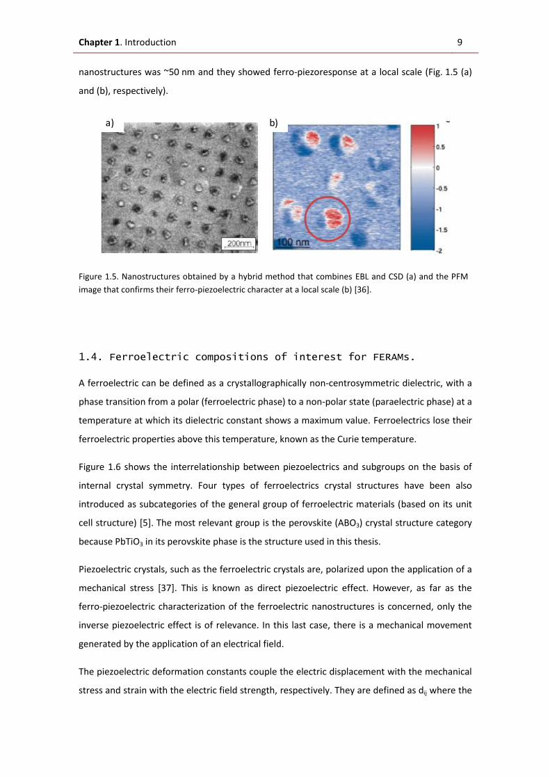
Chapter 1. Introduction 9
nanostructures was ~50 nm and they showed ferro-piezoresponse at a local scale (Fig. 1.5 (a)
and (b), respectively).
Figure 1.5. Nanostructures obtained by a hybrid method that combines EBL and CSD (a) and the PFM
image that confirms their ferro-piezoelectric character at a local scale (b) [36].
1.4. Ferroelectric compositions of interest for FERAMs.
A ferroelectric can be defined as a crystallographically non-centrosymmetric dielectric, with a
phase transition from a polar (ferroelectric phase) to a non-polar state (paraelectric phase) at a
temperature at which its dielectric constant shows a maximum value. Ferroelectrics lose their
ferroelectric properties above this temperature, known as the Curie temperature.
Figure 1.6 shows the interrelationship between piezoelectrics and subgroups on the basis of
internal crystal symmetry. Four types of ferroelectrics crystal structures have been also
introduced as subcategories of the general group of ferroelectric materials (based on its unit
cell structure) [5]. The most relevant group is the perovskite (ABO3) crystal structure category
because PbTiO3 in its perovskite phase is the structure used in this thesis.
Piezoelectric crystals, such as the ferroelectric crystals are, polarized upon the application of a
mechanical stress [37]. This is known as direct piezoelectric effect. However, as far as the
ferro-piezoelectric characterization of the ferroelectric nanostructures is concerned, only the
inverse piezoelectric effect is of relevance. In this last case, there is a mechanical movement
generated by the application of an electrical field.
The piezoelectric deformation constants couple the electric displacement with the mechanical
stress and strain with the electric field strength, respectively. They are defined as dij where the
a) b)

10 1.4. Ferroelectric compositions of interest for FeRAMs
first subscript refers to the direction of the electric field and the second one to the direction of
the mechanical stress or deformation. Thus, d33, d31 and d15 are defined, respectively, as the
longitudinal coupling factor (the displacement occurs in the same direction than the field), the
transverse coupling factor (the displacement is perpendicular to the field) and the shear
coupling factor (the shear is perpendicular to the field) [38].
Figure 1.6. Interrelationship of piezoelectric and subgroups on the basis of symmetry [5].
Pyroelectricity is the alteration of the spontaneous polarization with temperature and is a
symmetry property of crystals. Ferroelectric materials are, thus, piezoelectric and pyroelectric
materials which spontaneous polarization can be reverse by applying an electric field (coercive
field).
1.4.1. PbTiO3 perovskite structure.
The ferroelectric material used in this work is lead titanate (PbTiO3). It presents a perovskite
structure, as shown in Fig. 1.7.
At high temperatures (above ~490⁰C) it features cubic centrosymmetric phase, where the Pb2+
cations occupy the corner of the unit cell, the Ti4+ one, the central position and the O2- ions the
faces of the cell, forming an octahedron.
At lower temperatures (below ~490⁰C), PbTiO3 presents a tetragonal phase, where the c
(vertical) lattice parameter is elongated. The unit cell parameters of this phase are
a = b = 3.899(9) Å and c = 4.150(0) Å and its tetragonal distorsion c/a = 1.066(8), ~6.7%. In this
phase, there are two possible stable positions for the Ti4+ cation, both distortions along the c
(vertical) axis from the central position: above it or underneath it. As the center of the charges
32 symmetry point groups
21Noncentrosymmetric
11Centrosymmetric
20Piezoelectric
10Pyroelectric
SubgroupFerroelectric spontaneously
polarizedPolarization reversible
TungstenBronze
Oxygen octahedralABO3
Pyrochlore Layer structure
Chapter 1. Introduction 11
does not coincide with the center of the unit cell, there is a permanent dipole moment.
Therefore, these two positions can be related to the up and down polarization vector.
Figure 1.7. Perovskite structure of the PbTiO3 above ~490⁰C (a), below ~490⁰C (b) and representation of
the polarization states, as the Ti4+
cation can occupy the schematized two stable positions along the c-
axis. (c).
In the non-symmetric phase, two stable configurations are possible for the distribution of
charges in the primitive cell. Due to the small deformation, these configurations are separated
by a relatively small energy barrier. Therefore, a small electric field is enough to make one of
these configurations completely stable, while the other is unstable (process explained in Fig.
1.8 (a)-(d)). Thus, the dependence of the spontaneous polarization of a ferroelectric crystal
with the electric field has the shape shown in Fig 1.8 (e). This is general for any ferroelectric
material [39].
Lead titanate perovskite (PbTiO3) was chosen as material of study in this thesis due to the fact
that it does not exhibit phase transition in a wide range of temperature, its large tetragonality,
its high spontaneous polarization at room temperature (Ps > 50 μC/cm2) and the wide
temperature stability of the ferroelectric phase and its high Curie temperature (490 ⁰C). Both
polarization and Curie temperature are the highest among perovskite type structure
ferroelectric material [40]. As we are decreasing the size of the structures to the nanoscale, it
is expected the reduction of the properties of the material together with difficulties for its
characterization and, thus, the better the bulk properties for the material, the better we can
expect to study the ferroelectric nature of the nanostructures.

12 1.4. Ferroelectric compositions of interest for FeRAMs
Figure 1.8. Mechanical model schematized to explain the existence of dielectric hysteresis in any
ferroelectric crystal. (a) and (c) are the two stable states in the absence of an external electric field. The
potential well under electric fields of opposite directions is shown in (b) and (d). (e) represents the
hysteresis loop of a ferroelectric crystal under an external electric field, being the positions
corresponding to the (a)-(d) energy states marked with a red dot. The discontinuous lines mark the
transition from (a) and (b) states to (c) and (d) states (adapted from [39]).
1.5. Motivation and purpose of this work.
Since ferroelectricity is a collective phenomenon, certain minimum number of unit cells is
required. Therefore, the transition from the ferroelectric phase to a non-ferroelectric phase
must occur if the volume of the nanostructures is decreased beyond a limit [41]. A second
problem is that, as small volume nanostructures, the number of unit cells in the surface or the
interface between the nanostructure and the substrate below with respect to the bulk
nanostructure is large. Thus, there will be a larger influence of the surface effects on the
general behavior of the nanostructure.
The aim of this thesis is, on one hand, the development of a technique capable of produce
ferroelectric nanostructures periodically ordered of controlled size and shape. On the other
hand, there is a second scope: the preparation of real systems in order to study basic problems
of nanoferroelectric materials, related to the scale of the size and the surface effects. For that,
ferroelectric nanostructures of PbTiO3 in its perovskite phase will be prepared using a bottom-
U
z
U
z
U
z
U
z
a)
c)
b)
d)
P
E
a
c
b
d
e)

Chapter 1. Introduction 13
up method. This procedure will ensure that the nanostructures are grown damage-free, unlike
the ones prepared from any of the top-down procedures, as it was explained previously and,
thus, that the size and surface effects observed are those caused by the scaling of the size of
the nanostructure rather than by the preparation technique.
14 Bibliography
Bibliography
[1] R.B. Gray. Transducer and method of making the same. 1949.
[2] I. Bretos, "Low-toxic chemical solution deposition methods for the preparation of
multifunctional (Pb1-xCax)TiO3 thin films", Departamento de Química Inorgánica, 2006, Madrid:
Universidad Autónoma de Madrid. Ph.D. Thesis.
[3] J. Valasek, "Piezoelectric and allied phenomena in Rochelle salt", Physical Review, 15,
1920, p:537
[4] N. Setter and R. Waser, "Electroceramic materials", Acta Materialia, 48, 2000, p:151
[5] G.H. Haertling, "Ferroelectric ceramics: history and technology", Journal of the
American Ceramic Society, 82 (4), 1999, p:797
[6] N. Setter, "Electroceramics: looking ahead", Journal of the European Ceramic Society,
21, 2001, p:1279
[7] C.H. Ahn, K.M. Rabe and J.M. Triscone, "Ferroelectricity at the nanoscale: Local
polarization in oxide thin films and heterostructures", Science, 303 (5657), 2004, p:488
[8] D.D. Fong, G.B. Stephenson, S.K. Streiffer, J.A. Eastman, O. Auciello, P.H. Fuoss and C.
Thompson, "Ferroelectricity in ultrathin perovskite films", Science, 304 (5677), 2004, p:1650
[9] J. Junquera and P. Ghosez, "Critical thickness for ferroelectricity in perovskite ultrathin
films", Nature, 422 (6931), 2003, p:506
[10] A.N. Morozovska, E.A. Eliseev and M.D. Glinchuk, "Ferroelectricity enhancement in
confined nanorods: Direct variational method", Physical Review B, 73 (21), 2006,
[11] Naumov, II, L. Bellaiche and H.X. Fu, "Unusual phase transitions in ferroelectric
nanodisks and nanorods", Nature, 432 (7018), 2004, p:737
[12] J.E. Spanier, A.M. Kolpak, J.J. Urban, I. Grinberg, O.Y. Lian, W.S. Yun, A.M. Rappe and H.
Park, "Ferroelectric phase transition in individual single-crystalline BaTiO3 nanowires", Nano
Letters, 6 (4), 2006, p:735
[13] W.S. Yun, J.J. Urban, Q. Gu and H. Park, "Ferroelectric properties of individual barium
titanate nanowires investigated by scanned probe Microscopy", Nano Letters, 2 (5), 2002,
p:447
[14] J.F. Scott, Ferroelectric memories. Advanced microelectronics, ed. K. Itoh and T.
Sakurami. 2000, Berlin: Springer.
[15] C. Sealy, "Winning the memory race", Materials today, 11 (6), 2008, p:16
[16] G.I. Meijer, "Who Wins the Nonvolatile Memory Race?", Science, 319, 2008, p:1625
[17] L.A. Zheng. Method of forming inside rough and outside smooth HSG electrodes and
capacitor structure. 2007; US7459746.

Bibliography 15
[18] Toshiba Develops World's Highest-Bandwidth, Highest Density Non-volatile RAM. 2009.
http://www.toshiba.co.jp/about/press/2009_02/pr0902.htm
[19] Toshiba Develops World's Fastest, Highest Density FeRAM. 2006.
http://www.toshiba.co.jp/about/press/2006_02/pr0701.htm
[20] M. Alexe, C. Harnagea and D. Hesse, "Non-conventional micro- and nanopatterning
techniques for electroceramics", Journal of Electroceramics, 12, 2004, p:69
[21] M. Alexe and D. Hesse, "Self-assembled nanoscale ferroelectrics", Journal of Materials
Science, 41, 2006, p:1
[22] C. Ganpule, A. Stanishevsky, Q. Su, S. Aggarwal, J. Melngailis, E. Williams and R.
Ramesh, "Scaling of ferroelectric properties in thin films", Applied Physics Letters, 75, 1999,
p:409
[23] C. Harnagea, M. Alexe, J. Schilling, J. Choi, R.B. Wehrspohn, D. Hesse and U. Gösele,
"Mesoscopic ferroelectric cell arrays prepared by imprint lithography", Applied Physics Letters,
83 (9), 2003, p:1827
[24] M. Alexe, C. Harnagea, D. Hesse and U. Gösele, "Patterning and switching of nanosize
ferroelectric memory cells", Applied Physics Letters, 75, 1999, p:1793
[25] M. Alexe, C. Harnagea, D. Hesse and U. Gösele, "Polarization imprint and size effects in
mesoscopic ferroelectric structures", Applied Physics Letters, 79, 2001, p:242
[26] G.K. Hubler, Comparison and vacuum deposition techniques, in Pulsed Laser Deposition
of Thin Films, G.K.H. D. B. Chrisey, Editor. 1994, Wiley: New York.
[27] A. Milchev, Electrocrystallization. Fundamentals of nucleation and growth. 1st ed.
2002: Springer.
[28] J. Sun, P. Jina, Z.G. Wanga, H.Z. Zhangb, W. Z.Y. and L.Z. Hu, "Changing planar thin film
growth into self-assembled island formation by adjusting experimental conditions", Thin Solid
Films, 476, 2005, p:68
[29] M. Alexe, J.F. Scott, C. Curran, N.D. Zakharov, D. Hesse and A. Pignolet, "Self-patterning
nano-electrodes on ferroelectric thin films for gigabit memory applications", Applied Physics
Letters, 73 (11), 1998, p:1592
[30] W. Ma, M. Alexe and U. Gösele, "Formation of Ferroelectric Perovskite Nanostructure
Patterns Using Latex Sphere Monolayers as Masks: An Ambient Gas Pressure Effect during
Pulsed Laser Deposition ", Small, 1 (8-9), 2005, p:837
[31] W. Lee, H. Han, A. Lotnyk, M.A. Schubert, A. Senz, M. Alexe, D. Hesse, S. Baik and U.
Gösele, "Individually addressable epitaxial ferroelectric nanocapacitor arrays with near Tb
inch2 density", Nature nanotechnology, 3 (7), 2008, p:402

16 Bibliography
[32] D. Grosso, C. Boissiere, B. Smarsly, T. Brezesinski, N. Pinna, P.A. Albouy, H. Amenitsch,
M. Antonietti and C. Sanchez, "Periodically ordered nanoscale islands and mesoporous films
composed of nanocrystalline multimetallic oxides", Nature Materials, 3 (11), 2004, p:787
[33] I. Szafraniak, C. Harnagea, R. Schloz, S. Bhattacharyya, D. Hesse and M. Alexe,
"Ferroelectric epitaxial nanocrystals obtained by a self-patterning method", Applied Physics
Letters, 83 (11), 2003, p:2211
[34] S. Kronholz, S. Rathgeber, S. Karthauser, H. Kohlstedt, S. Clemens and T. Schneller,
"Self-assembly of diblock-copolymer micelles for template-based preparation of PbTiO3
nanograins", Advanced Functional Materials, 16 (18), 2006, p:2346
[35] S. Bühlmann, P. Muralt and S. Von Allmen, "Lithography-modulated self-assembly of
small ferroelectric Pb(Zr,Ti)O3 single crystals", Applied Physics Letters, 84, 2004, p:2614
[36] S. Clemens, S. Rohrig, A. Rudiger, T. Schneller and R. Waser, "Embedded ferroelectric
nanostructure arrays", Nanotechnology, 20 (7), 2009, p:5
[37] B. Jaffe, W.R. Cook and H. Haffe. 1971, New York: Academic Press.
[38] B. Jaffe, W.R. Cook and H. Haffe, Piezoelectric Ceramics. 1971, New York: Academic
Press.
[39] B.A. Strukov and A.P. Levanyuk, Principios de ferroelectricidad. 1988, Madrid: Ediciones
de la Universidad Autónoma de Madrid.
[40] B.A. Tuttle, D.A. Payne and J.L. Mukherjee, "Spontaneous Polarization for ferroelectric
materials", MRS bulletin, 19 (7), 1994, p:20
[41] A. Roelofs, T. Schneller, K. Szot and R. Waser, "Towards the limit of ferroelectric
nanosized grains", Nanotechnology, 14, 2003, p:250
CHAPTER 2: EXPERIMENTAL PROCEDURE
In this chapter, the details of the preparation process of the nanoparticles as well as the
explanation of the methods for the characterization of their properties will be presented.
2.1. Precursor solutions.
Nanoparticles will be prepared by deposition of a micellar solution onto the substrates by
three different procedures that will be explained in this Experimental Procedure Chapter. For
the preparation of micellar solutions, a PbTiO3 sol and a microemulsion are mixed. The
procedures to obtain those are here described.
2.1.1. Synthesis of the sol.
The precursor sol was synthesized using the route generally known in the literature as the
“diol-route” [1]. Therefore, lead (II) acetate trihydrate (Pb(OCOCH3)2·3H20, Aldrich, 99%) and
1,3-propanediol (HO(CH2)3OH, Aldrich 98%) were refluxed in air at ~ 155°C for 1 h. Then,
titanium (IV) di-isopropoxide bis-acetylacetonate (Ti(OC3H7)2(CH3COCHCOCH3)2, Aldrich,
75 wt% solution in 2-propanol) was added to the mixture and reflux was maintained in air at
~110°C for 8 h. After this step, byproducts were partially distilled off the solution. The volume
of the distilled liquid was the 80% volume of the total 2-propanol (CH3CHOHCH3) that the
synthesized sol contains [2]. An air stable and precipitate-free Pb(II)-Ti(IV) sol was obtained.
Stock sols are obtained with an average concentration of ~1.44 M (equivalent moles of PbTiO3
per liter of sol) and ~1.46 g/ml of density. Fig. 2.1. schematizes the route of synthesis.
Figure 2.1. Synthesis of the sol.
Pb(OCOCH3)2·3H2O + HO(CH2)3OH
Ti(OC3H7)2(CH3COCHCOCH3)2
Pb(II)-Ti(IV) sol
Reflux in air (155°C, 1h)
Ti (IV):1,3 propanediol1:5

18 2.1. Precursor solutions
2.1.2. Preparation of the microemulsion.
Microemulsions were prepared by mixing 0.420 g of Brij-30 (CH3(CH2)12(OCH2CH2)4OH, Aldrich
99%), 1.950 g of cyclohexane (C6H12, Aldrich, 99+%) and 0.034 g of deionized water. The
water:surfactant ratio is 1.0:1.6. The water-clear appearance of the mixture upon vigorous
stirring indicated the formation of the microemulsion. Fig. 2.2. schematizes the preparation
method.
Figure 2.2. Preparation of the microemulsion.
The microemulsions were kept for 24h and ultrasonically stirred for 10 minutes before the
deposition step.
2.1.3. Preparation of the micellar solution
The micellar solutions were prepared by mixing the sol with the microemulsion and adding 1,3-
propanediol (HO(CH2)3OH, Aldrich, 98%) to obtain the desired concentration. The preparation
method is schematized in Fig. 2.3.
Figure 2.3. Preparation of the micellar solution.
Brij-300.420 g
C6H12
1.950 g
Deionized H2O0.034 g
Microemulsion
Brij-30:H2O1.0:1.6
Microemulsion Pb(II)-Ti(IV) sol
1,3-propanediol
Micellar solution
Chapter 2: Experimental procedure 19
The micellar solutions were kept for 24 h and ultrasonically stirred for 10 minutes before the
deposition step.
Micellar solutions were also prepared by adding Ethyl-Hexanol and deionized water. Water
caused the precipitation of the sol, and was, thus avoided in the preparation of micellar
solution. Ethyl-Hexanol, instead was immiscible with cyclohexane. Thus, 1,3-propanediol was
chosen as solvent.
2.2. Selection of substrates.
Two different types of substrates were chosen for the fabrication of the nanostructures. A
polycrystalline substrate -Pt-coated Si(100) substrates-, compatible with the current Si
technology, and a single-crystal one –SrTiO3-, chosen because its crystal structure similarity
which, in addition, is supposed to lead to epitaxial growth.
2.2.1. Pt-coated Si(100) substrates
Selected Pt-coated Si(100) substrates are formed by Pt/TiO2/SiO2/(100)Si. The SiO2 layer
appears spontaneously when Si is in contact with air. Pt and TiO2 layers are deposited onto the
Si wafer (Crystal GmbH) by radiofrequency magnetron sputtering (Alcatel SCM 450) at the
“Laboratorio de sensores” of the “Centro de Tecnologías Físicas Leonardo Torres Quevedo”
(CSIC) in Madrid, with resulting thickness of ~100 nm and ~50 nm for the Pt and the TiO2,
respectively.
The substrates were cleaned before the deposition by ultrasonically soaking them in
trichloroethylene (Cl2CClCH, Panreac, stabilized with ethanol, 99%) for 5 min, in acetone
(CH3COCH3, Panreac, 99.5%) for 4 min and in 2-propanol (CH3CHOHCH3, Panreac, 99.5%) for
3 min, consecutively.
2.2.2. Microemulsion/Pt-coated Si(100) substrates
Functionalized substrates were prepared by depositing a layer of microemulsion by spin-
coating (50 s, 2000 rpm) onto the cleaned Pt/TiO2/SiO2/(100)Si substrates described in
previous subsection 2.2.1.
2.2.3. (100)SrTiO3 substrates
Commercial SrTiO3 (STO) and Nb-doped SrTiO3 substrates from Crystal GmbH are used in this
work as-served, without additional cleaning.

20 2.2. Selection of substrates
2.2.4. (100)SrTiO3 substrates with controlled surfaces
Chemical treatments of the substrates consisted on two different procedures: in the first one,
substrates were soaked in an etching solution (Buffered Hydrofluoric Acid, BHF, pH 4.5, 20 s);
in the second one, they were ultrasonically soaked in deionized water for 10 min and then
soaked in an etching solution (BHF, pH 5.5, 30 s).
BHF with pH 4.5 was prepared by adding 9.69 g of ammonium fluoride (NH4F, Aldrich, 98+%) to
10 ml of deionized water. Hydrofluoric acid (HF, Panreac, 99%) was added up to pH 4.3
(measured with a Thermo scientific Orion pHmeter). Deionized water is added up to complete
25 ml in order to obtain a 10 M ammonium fluoride solution.
BHF with pH 5.5 was prepared by adding 9.69 g ammonium fluoride to 10 ml of deionized
water. Hydrofluoric acid was added up to pH 5.5. Deionized water is added up to complete 25
ml.
Figure 2.4. Thermal treatments in UHV applied to the STO substrates.
Three different thermal treatments (annealings) were carried out with no oxygen flow,
contrary to the processes described previously in the literature [3, 4]. Substrates were
annealed in Ultra High Vacuum (UHV) using a radiative furnace, with the heater facing sample
backside and feedback controlled by a PID system. Since the furnace thermocouple was
located close to the substrate, but not in direct contact with it, the temperature of the STO
surface was calibrated by means of radiation thermometry at the center of the test Si(100)
~0.1 °C
815 ± 5 °C, 3600s
~0.03 °C
~0.2 °C
842 ± 7 °C, 7200s
~0.09 °C
a)
b)
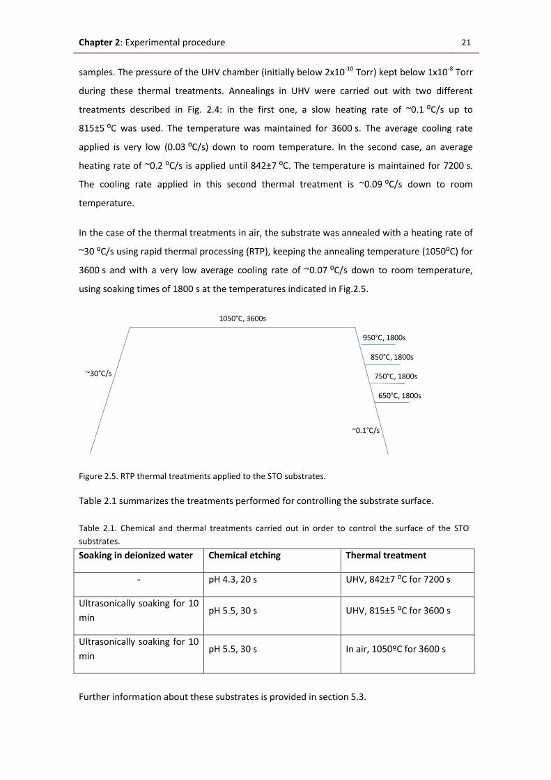
Chapter 2: Experimental procedure 21
samples. The pressure of the UHV chamber (initially below 2x10⁻¹⁰ Torr) kept below 1x10⁻⁸ Torr
during these thermal treatments. Annealings in UHV were carried out with two different
treatments described in Fig. 2.4: in the first one, a slow heating rate of ~0.1 ⁰C/s up to
815±5 ⁰C was used. The temperature was maintained for 3600 s. The average cooling rate
applied is very low (0.03 ⁰C/s) down to room temperature. In the second case, an average
heating rate of ~0.2 ⁰C/s is applied until 842±7 ⁰C. The temperature is maintained for 7200 s.
The cooling rate applied in this second thermal treatment is ~0.09 ⁰C/s down to room
temperature.
In the case of the thermal treatments in air, the substrate was annealed with a heating rate of
~30 ⁰C/s using rapid thermal processing (RTP), keeping the annealing temperature (1050⁰C) for
3600 s and with a very low average cooling rate of ~0.07 ⁰C/s down to room temperature,
using soaking times of 1800 s at the temperatures indicated in Fig.2.5.
Figure 2.5. RTP thermal treatments applied to the STO substrates.
Table 2.1 summarizes the treatments performed for controlling the substrate surface.
Table 2.1. Chemical and thermal treatments carried out in order to control the surface of the STO
substrates.
Soaking in deionized water Chemical etching Thermal treatment
- pH 4.3, 20 s UHV, 842±7 ⁰C for 7200 s
Ultrasonically soaking for 10
min pH 5.5, 30 s UHV, 815±5 ⁰C for 3600 s
Ultrasonically soaking for 10
min pH 5.5, 30 s In air, 1050ºC for 3600 s
Further information about these substrates is provided in section 5.3.
1050°C, 3600s
~30°C/s
950°C, 1800s
850°C, 1800s
750°C, 1800s
650°C, 1800s
~0.1°C/s

22 2.3. Deposition, drying and crystallization of the PbTiO3 nanostructures
2.3. Deposition, drying and crystallization of the PbTiO3
nanostructures.
The deposition of the micellar solutions has been carried out by spin-coating. This process can
be divided into four stages [5]: deposition, spin-up, spin-off and evaporation, as shown in Fig.
2.6. During the deposition stage, a liquid excess is dispensed onto the substrate surface. This
liquid flows radially outward in the spin-up stage, driven by centrifugal force. In the spin-off
stage, the liquid excess flows to the perimeter of the substrate surface and leaves it as droplets.
Finally, evaporation of solvent occurs during the last stage.
Figure 2.6. Spin-coating process.
Glass syringes equipped with non-sterile plastic nozzles and coupled with filters (Millipore) of
0.2 µm pore size were used in the deposition of the sols for the nanostructures fabricated by
using the phenomenon of the microstructural instability of polycrystalline ultrathin films. In
the case of nanostructures prepared by using micellar solution, no filters had been used, as the
micelles size is larger (see section 4.2 for further details) than the pore size of the filters.
Spin-coating was carried out in a spinner equipment (TP 6000 gyrset system of SET-Micro-
Controle group model), working at 2000 rpm for 45 s.
When fabricating nanostructures by using the phenomenon of the microstructural instability
of polycrystalline ultrathin films, the wet precursor films thus obtained were dried and
pyrolysed in order to remove the entrapped solvent and the majority of the organic species
present within the gel network. The wet layer was subjected to a thermal treatment on a hot
plate (Selecta) stabilized at 350 ⁰C for 60 s.
In the case of the fabrication of nanostructures by the microemulsion mediated synthesis, in
order to promote their evaporation induced self-assembly, the micellar layer was dried at
ω
ω
dω/dt≠0
ω ω
Deposition Spin-up Spin-off Evaporation

Chapter 2: Experimental procedure 23
~30 ⁰C for 7 days in an oven and the relative humidity was kept constant at ~30 % (controlled
by an hygrometer HD2101.2 by Delta Ohm).
The coatings so obtained were crystallized into the desired oxide phase (i.e. perovskite) by
Rapid Thermal Processing (RTP, carried out at a Jetstar 100T JIPELEC equipment). The samples
were annealed in air at 650 ⁰C for 50 s with a heating and cooling rate of 30 ⁰C/s. Fig. 2.7.
shows the thermal program used for the crystallization of the PbTiO3 nanostructures.
Figure 2.7. Thermal recipe used for the crystallization of the nanostructures.
2.4. Microscopy and quantitative microstructure characterization
A description and fundamental definitions concerning the characterization techniques of the
microstructures used in this work are given in the following sections.
2.4.1. Optical microscopy
Optical microscopy images were obtained with an optical microscope, at x22 magnification.
Calibration of the images was done with a micrometer (Leitz).
2.4.2. Scanning Electron Microscopy
The Scanning Electronic Microscopy (SEM) [6] is based on the use of a beam of highly energetic
electrons to examine objects at a very fine scale. In SEM, the image is formed by an electron
beam which is focused on the specimen surface. This beam is first produced at the top of the
microscope by a thermoionic electron gun. Electrons are accelerated towards the specimen
using a positive electric potential of 2-40 kV. The electron beam is confined and focused using
metal apertures and magnetic lenses into a thin, monochromatic beam, directed down to the
sample. The interaction between the primary electrons and the sample gives rise to various
physical phenomena (backscattering, cathodoluminiscence, secondary electrons, x-ray, Auger
emission, etc). In the case of SEM, the detector collects secondary electrons and converts
them into a signal that is sent to a viewing screen, producing thus an image. Secondary
600 ⁰C
650 ⁰C, 50s
1s
1s
1s1s
1s
1s
550 ⁰C
500 ⁰C
100 ⁰C
20s

24 2.4. Microscopy and quantitative microstructure characterization
electrons are excited electrons of the specimen produced by the inelastic collision with the
primary electron beam which results ejected from the atoms and, after undergoing additional
scattering events while travelling through the sample, emerged from its surface with a low
energy value (< 50 eV). Due to this low energy, only secondary electrons that are near the
surface can escape and be examined. Hence, the information obtained by SEM is related to the
topography of the sample.
SEM images of this work have been obtained in three different electronic microscopes: JSM
6335F NT (FEG-SEM) microscope at the “Centro de Microscopía Electrónica Luís Bru” of the
“Universidad Complutense de Madrid” at Madrid, a Philips ESEM XL 30 FEG at the
Interdisziplinäres Zentrum für Materialwissenschaften at Halle (Germany) and a FEI XL30-SFEG
at Cranfield University at Cranfield (United Kingdom).
2.4.3. Transmission electron microscopy (TEM)
A transmission electron microscope essentially works as a SEM one, with the main difference
that the image formed by TEM (Transmission Electron Microscopy) is obtained from the
electrons transmitted through the specimen [7]. Since electronic absorption by the sample is
much more efficient than electronic transmission through it, TEM microscopes usually work
with a high voltage electron beam of 80-400 keV. Furthermore, materials for TEM analysis
must be specially thinned to get specimens which allow electrons to be transmitted through
them (100-200 Å thickness).
A TEM microscope basically consists in a column, set at ultrahigh vacuum, where the
illumination system is displayed along. The electron gun produces a high-energy stream of
monochromatic electrons which are focused into a thin, coherent beam by the use of
condenser lenses. The first lens determines the spot size (general size range of the final spot
that strikes the sample), whereas the second one controls its intensity (from a wide dispersed
spot to a pinpoint beam). The beam is restricted by the condenser aperture until it strikes the
specimen and parts of the electrons are transmitted through. The transmitted electrons are
focused by the objective lens into an intermediate image, which is enlarged by the
intermediate and projector lenses until it impinges on a phosphor image screen and light is
generated, allowing the user to see the image.
Two types of information (images) can be obtained; the direct image projected by the entire
specimen (microstructure) and the electron diffraction pattern resulted when the electron
beam crosses an orderly crystallographic pattern (crystallographic structure). With the
Chapter 2: Experimental procedure 25
objective aperture the image contrast is enhanced by blocking out high-angle diffracted
electrons, whereas the selected area aperture allows collecting the diffraction patters
obtained. From the electron diffraction patterns, the interplanar distances dhkl and indexation
of planes {hkl} were calculated, according to Bragg’s Law and assuming low diffraction angles θ,
by the following expression
𝑑ℎ𝑘𝑙 = 𝜆𝐿/𝑅 (2.1)
where L is the camera length of the microscope (specimen-screen distance), λ is the
wavelength of the electron beam and R is the distance of the diffracted spot respect to the
incident beam position (in the electron pattern).
TEM images can be bright or dark field ones. Bright field images are obtained by opening the
lens of the microscope, which eliminates the diffracted beams. In contrast, each diffracted
beam form an image called dark field image in which the maximum intensity is observed for
the portions of the sample that diffracts in a certain angle.
TEM measurements have been carried out at the “Universidad Carlos III de Madrid”, in Madrid
(Spain), using a JEOL-200 FX II microscope operating at 200 kV. Cross section specimens of the
films were prepared from two pieces of the sample which were stacked with the
nanostructures layers facing and glued. Lateral thickness was decreased until 20 µm, using a
tripod polisher. Large electron-transparent areas were obtained by Ar+ ion milling (acceleration
voltage of 5 kV, beam intensity of 5 mA and incidence angle between 8-10°).
2.4.4. Scanning Probe Microscopy
Scanning Probe Microscopy (SPM) [8, 9] is a general name for a group of techniques in which a
sharp probe scans the surface of a sample, measuring some property of it. The tip is mounted
onto a flexible cantilever of known geometrical and material properties, so that it is possible to
separate all the contributions of the interaction with a high sensitivity. The interactions of the
tip with the sample are sensed by the resultant deflection of the cantilever onto which the tip
is mounted. This deflection is measured by reflecting a laser beam off the cantilever. The
reflected laser beam strikes a position-sensitive photo-detector consisting of four-segment
photo-detector. The differences of the intensity of the signals between the segments of photo-
detector indicate the position of the laser spot on the detector and thus the angular
deflections of the cantilever.

26 2.4. Microscopy and quantitative microstructure characterization
A typical SPM system consists of a tip mounted onto a cantilever, a xyz piezo-scanner attached
either to the sample or to the cantilever, a laser and a deflection sensor or detector as
schematized in Fig. 2.8.
Figure 2.8. Experimental set-up of a SPM system.
As explained before, the sample investigation is possible by studying the forces acting between
the sharp probe and the surface of the sample. Depending on the distance between them, one
or another force dominates the system, that is to say, they are position-dependent. Fig. 2.9
represents the force-distance curve for the interaction between the probe and the sample.
Figure 2.9. Force-distance curve of the interaction between the probe tip and the sample surface.
Depending on the point of the curve where measurements take place, images might be
acquired in contact, intermittent-contact or non-contact modes.
detector
sample
XYZ piezo-scanner
cantilever
Laser beam
tip
Forc
e(F
)
Distance (d)
Repulsive forces
Attractive forces
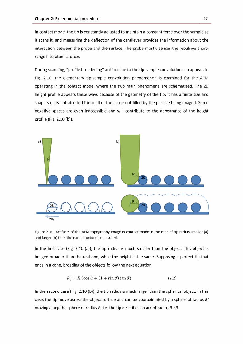
Chapter 2: Experimental procedure 27
In contact mode, the tip is constantly adjusted to maintain a constant force over the sample as
it scans it, and measuring the deflection of the cantilever provides the information about the
interaction between the probe and the surface. The probe mostly senses the repulsive short-
range interatomic forces.
During scanning, "profile broadening" artifact due to the tip-sample convolution can appear. In
Fig. 2.10, the elementary tip-sample convolution phenomenon is examined for the AFM
operating in the contact mode, where the two main phenomena are schematized. The 2D
height profile appears these ways because of the geometry of the tip: it has a finite size and
shape so it is not able to fit into all of the space not filled by the particle being imaged. Some
negative spaces are even inaccessible and will contribute to the appearance of the height
profile (Fig. 2.10 (b)).
Figure 2.10. Artifacts of the AFM topography image in contact mode in the case of tip radius smaller (a)
and larger (b) than the nanostructures, measured.
In the first case (Fig. 2.10 (a)), the tip radius is much smaller than the object. This object is
imaged broader than the real one, while the height is the same. Supposing a perfect tip that
ends in a cone, broading of the objects follow the next equation:
𝑅𝑐 = 𝑅 cos𝜃 + 1 + sin𝜃 tan𝜃 (2.2)
In the second case (Fig. 2.10 (b)), the tip radius is much larger than the spherical object. In this
case, the tip move across the object surface and can be approximated by a sphere of radius R’
moving along the sphere of radius R, i.e. the tip describes an arc of radius R’+R.
θ
2R
2R0
a)
R’2R
R’2R
b)

28 2.4. Microscopy and quantitative microstructure characterization
A second mode of operating is the so called, intermittent-contact, dynamic mode or tapping
mode. In this mode [10-13], the cantilever is forced by an actuator placed at its base to
oscillate up and down at its resonant frequency. Part of the oscillation extends into the
repulsive regime, so the tip intermittently touches or “taps” the surface. This is the reason why
this mode is also referred as tapping mode. Constant amplitude is maintained by a feedback
mechanism while scanning the sample. In this manner an image of the surface topography is
generated [14]. Fig. 2.11 shows how oscillation resonant frequency shifts with the repulsive or
attractive forces between the sample and the probe.
Figure 2.11. Resonant frequency shift when the probe is affected by attractive or repulsive forces.
Tapping or intermittent-contact mode tends to be more applicable to general imaging in air,
particularly for soft samples, as the lateral resolution is higher than in contact mode while the
forces applied to the sample are lower and less damaging.
In non-contact mode, the cantilever-tip system vibrates at its resonant frequency above the
sample and the changes in the topography are detected by changes in the amplitude or the
phase of the vibration. It is basically the same as tapping mode, but the tip never touches the
sample. This can lead to artifacts such as imaging water drops on the surface as if they were
part of the topography of the samples.
ωR ω'Rω‘’R
Δω
ΔA
AR
A’R
A
ω
Attractive forces Repulsive forces

Chapter 2: Experimental procedure 29
Atomic Force Microscopy (AFM) is a SPM technique based on the detection of the topography
of the surface by measuring the atomic force between the tip probe and said surface. In this
work, AFM topography images are acquired with a commercial SPM microscope (Nanotec
Electronica) controlled by WSxM software [15]. The probe used in this work (Nanosensors) is
presented in Fig. 2.12.
Figure 2.12. Nanosensors probes for the acquisition of AFM topography images.
2.4.4.1. Fast Fourier Transform and self-convolution images.
Self-correlation is defined as [16]:
𝐺 𝑘1 ,𝑘2 = 𝑓 𝑥,𝑦 · 𝑓 𝑥 + 𝑘1,𝑦 + 𝑘2 (2.3)
Where f(x,y) is the image matrix. This equation takes the image and the same image is shifted
a distance k1 and k2 in the X and Y axis with respect to the center of the image. The resulting
image, G(k1, k2), is a measure of how different the two images are. The more similar the image
and the shifted image are, the higher the value of the self correlation. In self-correlation, the
highest value is obtained at the center of the image (where k1 and k2 are zero). Any periodicity
in the original image will be shown as a periodic pattern in the self correlation.
The Fast Fourier Transform (FFT) is an efficient algorithm to compute the Discrete Fourier
Transform (DFT) and its inverse, reducing the number of computations needed for N points
from 2·N2 to 2·N·log2N. DFT is a generalized case of the Continuous Fourier Transform for a
discrete function and it is extremely useful because it reveals periodicity in input data as well
as the relative strengths of any periodic components by transposing from time-domain to
frequency-domain [16]. The DFT can be transformed efficiently using a FFT.
In the system used in this work, SPM signals are discrete and obtained by using an Analogical
to Digital Converter (ADC) chip placed at the Digital Signal Processor (DSP). The DSP do not
perform integral calculus and thus, the signal is obtained by smashing numbers using the
“Butterfly” algorithm [16]. This algorithm is a standard procedure that implements the
SSS-NCH• SuperSharpSilicon - tip• Non-Contact High frequency• C = 42 N/m, fo = 330 kHz
PPP-NCH• Pointprobe® Plus - tip• Non-Contact High frequency• C = 42 N/m, fo = 330 kHz
PPP-NCHPt• Pointprobe® Plus - tip• Non-Contact High frequency• C = 42 N/m, fo = 330 kHz• PtIr5 coated probe
PPP-CONT• Pointprobe® Plus - tip• Contact Mode
• C = 0.2 N/m, fo = 13 kH

30 2.4. Microscopy and quantitative microstructure characterization
numeric conversion of a time-domain signal into a frequency spectrum, being both discrete,
performing the FFT.
Figure 2.13 illustrates the self-correlation and the FFT filter of a high order sample.
Figure 2.13. Original sample (a), image after applying the FFT filter (b) and self-correlated image (c).
2.4.5. Image analyses.
Size distribution of the nanostructures fabricated in this work will be obtained by
measurements on microscopy images and analyzed later by a graphic method using probability
plots. This allows the precise determination of average values and standard deviations of the
distributions. And, besides, microstructural phenomena that escape the less detailed
microstructural analysis are easily studied, like the process of normal grain growth [17]. For
example it has been used for the study of relevant phenomena concerning microstucture-
properties relationships in piezoceramics such as the ones presented in Fig. 2.14.
Figure 2.14. Study the porosity reduction and microstructure recovery from the degraded sintering
stage by subsequent Hot isostatic pressing (HIP) [18] (a) and the study the limit of the increase in grain
size without microstructure degradation by recrystallization of hot pressed samples in Aurivillius
ceramics [19] (b).
a) b) c)
(a)
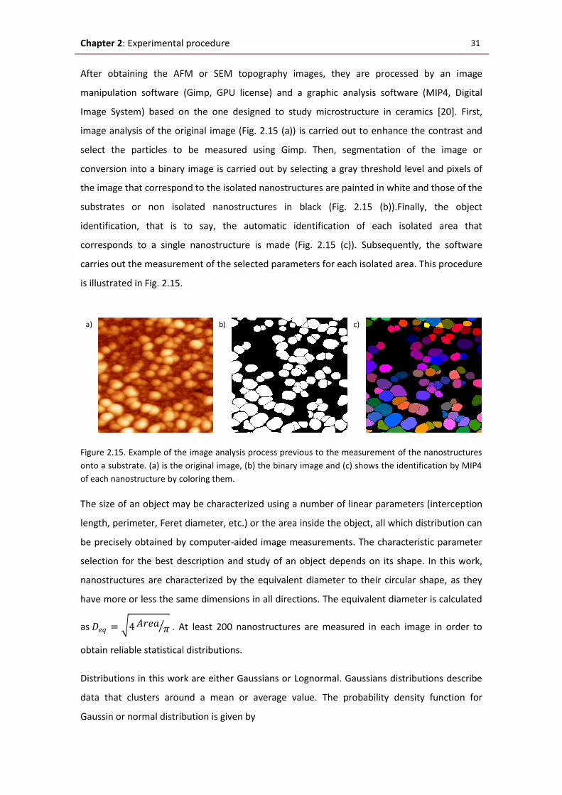
Chapter 2: Experimental procedure 31
After obtaining the AFM or SEM topography images, they are processed by an image
manipulation software (Gimp, GPU license) and a graphic analysis software (MIP4, Digital
Image System) based on the one designed to study microstructure in ceramics [20]. First,
image analysis of the original image (Fig. 2.15 (a)) is carried out to enhance the contrast and
select the particles to be measured using Gimp. Then, segmentation of the image or
conversion into a binary image is carried out by selecting a gray threshold level and pixels of
the image that correspond to the isolated nanostructures are painted in white and those of the
substrates or non isolated nanostructures in black (Fig. 2.15 (b)).Finally, the object
identification, that is to say, the automatic identification of each isolated area that
corresponds to a single nanostructure is made (Fig. 2.15 (c)). Subsequently, the software
carries out the measurement of the selected parameters for each isolated area. This procedure
is illustrated in Fig. 2.15.
Figure 2.15. Example of the image analysis process previous to the measurement of the nanostructures
onto a substrate. (a) is the original image, (b) the binary image and (c) shows the identification by MIP4
of each nanostructure by coloring them.
The size of an object may be characterized using a number of linear parameters (interception
length, perimeter, Feret diameter, etc.) or the area inside the object, all which distribution can
be precisely obtained by computer-aided image measurements. The characteristic parameter
selection for the best description and study of an object depends on its shape. In this work,
nanostructures are characterized by the equivalent diameter to their circular shape, as they
have more or less the same dimensions in all directions. The equivalent diameter is calculated
as 𝐷𝑒𝑞 = 4𝐴𝑟𝑒𝑎𝜋 . At least 200 nanostructures are measured in each image in order to
obtain reliable statistical distributions.
Distributions in this work are either Gaussians or Lognormal. Gaussians distributions describe
data that clusters around a mean or average value. The probability density function for
Gaussin or normal distribution is given by
a) b) c)
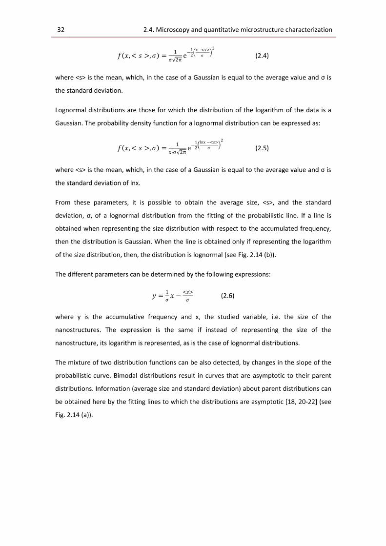
32 2.4. Microscopy and quantitative microstructure characterization
𝑓 𝑥, < 𝑠 >,𝜍 =1
σ 2πe−
1
2
x−<𝑠>
σ
2
(2.4)
where <s> is the mean, which, in the case of a Gaussian is equal to the average value and σ is
the standard deviation.
Lognormal distributions are those for which the distribution of the logarithm of the data is a
Gaussian. The probability density function for a lognormal distribution can be expressed as:
𝑓 𝑥, < 𝑠 >,𝜍 =1
x·σ 2πe−
1
2
lnx −<𝑠>
σ
2
(2.5)
where <s> is the mean, which, in the case of a Gaussian is equal to the average value and σ is
the standard deviation of lnx.
From these parameters, it is possible to obtain the average size, <s>, and the standard
deviation, σ, of a lognormal distribution from the fitting of the probabilistic line. If a line is
obtained when representing the size distribution with respect to the accumulated frequency,
then the distribution is Gaussian. When the line is obtained only if representing the logarithm
of the size distribution, then, the distribution is lognormal (see Fig. 2.14 (b)).
The different parameters can be determined by the following expressions:
𝑦 =1
𝜍𝑥 −
<𝑠>
𝜍 (2.6)
where y is the accumulative frequency and x, the studied variable, i.e. the size of the
nanostructures. The expression is the same if instead of representing the size of the
nanostructure, its logarithm is represented, as is the case of lognormal distributions.
The mixture of two distribution functions can be also detected, by changes in the slope of the
probabilistic curve. Bimodal distributions result in curves that are asymptotic to their parent
distributions. Information (average size and standard deviation) about parent distributions can
be obtained here by the fitting lines to which the distributions are asymptotic [18, 20-22] (see
Fig. 2.14 (a)).

Chapter 2: Experimental procedure 33
2.5. Structural characterization
2.5.1. Synchrotron X-Ray diffraction.
The crystalline structure of the nanostructures has been studied by synchrotron X-ray
diffraction in grazing incidence geometry.
Synchrotron radiation is usually defined as the electromagnetic radiation emitted by a
relativistic charged particle (generally electrons) moving on a circular orbit, e.g. in a
synchrotron. In a synchrotron, the electric (accelerating) and magnetic (deflecting) fields are
synchronized to ensure that the particles follow a prescribed geometric and energetic path
[23].
The emission of electromagnetical radiation from an accelerated charge is a classical
phenomenon [24]. In a synchrotron, centripetal acceleration generates an extremely intense
beam of synchrotron radiation that is emitted tangent to the charges (electrons) path. Under
the operation conditions of a synchrotron, the emitted radiation typically goes from ultraviolet
(1016 Hz) to X-ray (1018 Hz).
One of the sources of synchrotron radiation is wigglers. A wiggler consists on a series of
magnets designed to periodically laterally deflect ('wiggle') a beam of charged particles inside a
storage ring of a synchrotron and, thus, generate synchrotron radiation.
When an X-ray beam impinges on a crystal (i.e. periodically ordered of atoms) which
interatomic distances are about the same as the wave length (on the order of a few
angstroms), part of the waves can be scattered by the atoms present in the crystal. If the
scattered waves conserve the energy of the incident beam (elastic scattering) and are also able
to interfere with each other (coherence), the diffraction phenomenon may occur. The
diffraction arises when scattered beams are combined in phase with each other, producing an
unmoving distribution of constructive interference and, hence, a visible interference x-ray
pattern. All former conditions can be summarized in the Bragg’s Law:
2 · 𝑑ℎ𝑘𝑙 · sin𝜃 = 𝑛 · 𝜆 (2.7)
Where dhkl is the distance between scattering centers (atomic {hkl} planes), θ is the diffraction
angle, n is an integer known as the order of the diffracted beam and λ is the wavelength of the
incident beam.

34 2.5. Structural characterization
Each crystal presents a particular and characteristic diffraction pattern, since the different
interatomic distances between the {hkl} planes are specific from its primitive unit cell. In this
way, the unit cell vectors which define the structure of the crystal can be determined from the
X-ray diffraction patterns. On the other hand, the intensity of the diffracted beams is related to
the nature and arrangement of the atoms in the crystalline network. Intensity variations are
indicative of preferred orientation of one or more particular crystallographic planes in the
crystal.
The reciprocal lattice of a Bravais lattice of position vector 𝑅 is mathematically defined as the
lattice with position vectors 𝑘 that fulfills the next equation:
𝑒𝑖𝑘 𝑅 = 1 (2.8)
Each point (hkl) in the reciprocal lattice corresponds to a set of lattice planes (hkl) in the real
space lattice. The direction of the reciprocal lattice vector corresponds to the normal to the
real space planes, and the magnitude of the reciprocal lattice vector is equal to the reciprocal
of the interplanar spacing of the real space planes.
The reciprocal lattice plays a fundamental role in most analytic studies of periodic structures,
particularly in the theory of diffraction.
Ewald sphere was introduced in connection with the concept of the reciprocal lattice and is the
geometrical representation of the Bragg’s Law [25-27]. The aim of the Ewald sphere is to
determine which lattice planes (represented by the grid points on the reciprocal lattice) will
result in a diffracted signal for a given wavelength, λ, of incident radiation.
The incident plane wave falling on the crystal has a wave vector 𝑘𝑖 whose length is 2π / λ. The
diffracted plane wave has a wave vector 𝑘𝑓 . If no energy is gained or lost in the diffraction
process (it is elastic) then 𝑘𝑓 has the same length as 𝑘𝑖 . The difference between the wave-
vectors of diffracted and incident wave is defined as scattering vector ∆𝑘 = 𝑘𝑓 − 𝑘 𝑖. Since 𝑘𝑖
and 𝑘𝑓 have the same length, the scattering vector must lie on the surface of a sphere of
radius 2π / λ. This sphere is called the Ewald sphere. A 2-dimensional representations is shown
in Fig. 2.13.
The reciprocal lattice points are the values of momentum transfer where the Bragg diffraction
condition is satisfied and for diffraction to occur the scattering vector must be equal to a
reciprocal lattice vector. Geometrically this means that if the origin of reciprocal space is

Chapter 2: Experimental procedure 35
placed at the tip of 𝑘𝑖 , then diffraction will occur only for reciprocal lattice points that lie on
the surface of the Ewald sphere.
Figure 2.16. Ewald sphere 2-dimensional representation. Green points are the reciprocal lattice ones.
2.5.1.1. Grazing incidence
The conventional Bragg-Brentano geometry (θ-2θ) may, however, not be the best
configuration for the analysis of nanostructures, since reflections coming from the substrate
could overlap the diffraction pattern of the nanostructure. The asymmetric Bragg geometry,
also known as grazing incidence geometry, is used in the analysis of polycrystalline materials
onto substrates, as is the case of the nanostructures of this work. In this configuration, the
incidence angle θ is fixed at a certain value (α). Low incidence angles reduce the penetration of
the incident X-rays within the material and, therefore, reflections coming from the substrate
are minimized.
To determine the appropriate incidence angle to use in the grazing incidence X-ray diffraction,
the critical angle, αc, i.e. the angle below which, the total reflection of the X-rays takes place,
and the penetration depth of the X-rays for different α values were calculated for the PbTiO3
nanostrucures. The critical angle was calculated from the Snell’s law in total reflection
conditions [28] and from the refraction index for X-rays of a material [29] according to the
following expression:
sin𝛼𝑐 = 2.6 · 𝑒−6𝜌𝜆2 (2.9)
where ρ is the theoretical density of the material and (7.97 g/cm3 in the case of PbTiO3), λ is
the wavelength of the X-ray beam (0.97513 Å for this synchrotron radiation). The total
reflection for the PbTiO3 will occur at 0.41 °.
·· · · · · ·
·· · · · · ·
·· · · · · ··· · · · · ··· · · · · ·
·· · · · · ·
θθ
θ
ki
kf

36 2.5. Structural characterization
Therefore, incident angles below αc cannot be used in this experiment, since the total
reflection is produced.
The penetration depth of the X-ray beams through the film is related to the absorption of the
sample as:
𝐼 = 𝐼0𝑒−𝜇𝑥
sin 𝛼 (2.10)
where µ is the X-ray absorption coefficient of the material, x is the thickness of the material
penetrated by the X-rays and α is the incident angle of the X-rays. The equivalent penetration,
Λ, is defined as the thickness that is penetrated by X-rays of Io intensity in order to decrease
their intensity by 1/e:
Λ =sin 𝛼
𝜇 (2.11)
The µ value calculated for the PbTiO3 is 0.022 µm-1. Therefore, the penetration calculated for a
various incidence angles are:
α (°) 0.450 0.500 0.750 1.000 2.000
Λ (µm) 0.357 0.397 0.595 0.793 1.586
According to these values, angles above the critical angle that produce total reflection, will
yield penetration of substrates by the X-ray beam. The equivalent penetration is calculated
also for the Pt (which is the last layer of the Pt/TiO2/SiO2/(100)Si substrates) and the SrTiO3,
being µ, 0.455 µm-1 and 0.010 µm-1, respectively.
α (°) 0.450 0.500 0.750 1.000 2.000
Λ(Pt) (µm) 0.017 0.019 0.029 0.038 0.077
Λ(SrTiO3) (µm) 0.785 0.872 1.309 1.745 3.490
Therefore, diffraction experiments should take into account the substrate contributions to the
2-dimensional diffraction patterns.
In this work synchrotron X-ray diffraction experiments were carried out in grazing incidence at
the beamline station 11-3 of the Stanford Synchrotron Radiation Lightsource (SSRL) in Stanford
(USA). A monochromatic beam of 12.7 keV was generated by a 26 pole wiggler, vertically and
horizontally focused by a Rh coated flat mirror and a single crystal (311) bent monochromator,
respectively. The diffracted radiation is detected by an imaging plate detector of 345 mm of

Chapter 2: Experimental procedure 37
diameter with a pixel size of 150 µm x 150 µm (MAR345 image plate, Marresearch GmbH). Fig.
2.17 schematizes the configuration of the experiment.
Image 2.17. Schematic illustration of the grazing incidence geometry used for X-ray diffraction.
Imaging plate detectors are a kind of 2-dimensional detectors in which a layer of BaF(Br,I):Eu2+
that contains color centers is disposed onto a robust film-like base “plate”. The plate is then
exposed to the X-rays. The image is later scanned by an online scanner. Scanning the image
consists of exciting the colors centers and then detecting the induced radiation. Stimulating
color centers does not require much energy, generally red laser suffices.
The great advantages of imaging plates are their large size, low cost and their high dynamic
range. The latter quality has made it the detector of choice for 2-dimensional diffraction. Their
major drawback is the dead time associated with the time-consuming scanning [30].
A 2-dimensional plate and the detecting mechanism are schematized in Fig. 2.18. Red, green
and white points of the reciprocal lattice are those that fulfill the Law condition of diffraction.
The corresponding vectors are projected to the plate and will result into the final pattern. Note
that only the points which projection intersects the plate will yield excitation of the plate pixels
and, therefore, observed diffraction peaks.
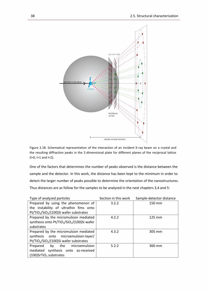
38 2.5. Structural characterization
Figure 2.18. Schematical representation of the interaction of an incident X-ray beam on a crystal and
the resulting diffraction peaks in the 2-dimensional plate for different planes of the reciprocal lattice
(l=0, l=1 and l=2).
One of the factors that determines the number of peaks observed is the distance between the
sample and the detector. In this work, the distance has been kept to the minimum in order to
detect the larger number of peaks possible to determine the orientation of the nanostructures.
Thus distances are as follow for the samples to be analyzed in the next chapters 3,4 and 5:
Type of analyzed particles Section in this work Sample-detector distance
Prepared by using the phenomenon of the instability of ultrathin fims onto Pt/TiO2/SiO2/(100)Si wafer substrates
3.2.2 150 mm
Prepared by the micromulsion mediated synthesis onto Pt/TiO2/SiO2/(100)Si wafer substrates
4.2.2 125 mm
Prepared by the micromulsion mediated synthesis onto microemulsion-layer/ Pt/TiO2/SiO2/(100)Si wafer substrates
4.3.2 305 mm
Prepared by the microemulsion mediated synthesis onto as-received (100)SrTiO3 substrates
5.2.2 360 mm

Chapter 2: Experimental procedure 39
Distances are varied depending on the relative intensities observed of the PbTiO3
nanostructures and the different substrates. It was explained before, that for angles above the
critical angles that produces total reflection, the penetration distance is larger than the height
of the nanostructures. The contribution of the substrates will depend not only on the
incidence angle but also on the orientation of the substrates crystallites or single-crystal planes
with respect to the incidence angle.
2-dimensional diffractions patterns are simulated by using Anaelu software [31-33]. When
crystals present a circular symmetry about some sample axis, they are said to have a fiber
texture. It is possible to calculate the inverse pole figure known the fiber texture and the unit
cell of crystals, and, from said inverse pole figure, the simulated diffraction pattern can be
calculated [34].
In this work, simulated diffraction patterns are calculated from the inverse pole figure and by
rotating the unit cell, using Anaelu software. The diagram flow of the iterative procedure for
the lattice parameters and texture of the nanostructures is schematized in Fig. 2.19.
Figure 2.19. Diagram flow of the iterative procedure for the lattice parameters (a) and texture of the
nanostructures (b).
b)
Simulated θ-2θ diffraction pattern
(PowderCell)
Comparasion with the integrated
pattern
Modification of lattice parameters
Experimental lattice parameters
a)Simulated 2-D
diffracion pattern (experimentals
parameters)(ANAELU)
Does ithave fiber
texture
Simulated diffraction pattern
from the IPF(ANAELU)
Comparasion with the integrated
pattern
Modification of texture
Experimental texture
determination
Simulated diffraction pattern
from the rotation of
the unit cell(ANAELU)
Comparasion with the integrated
pattern
Modification of texture
Experimental texture
determination
YES NO
Calculated latticeparameters fromthe experimental
patterns
Calculated latticeparameters fromthe experimental
patterns
Calculated latticeparameters fromthe experimental
patterns

40 2.5. Structural characterization
Fig. 2.20 shows a 2-dimensional pattern obtained when using the 2-dimensional diffraction
pattern.
Figure 2.20. 2-dimensional X-ray transmission pattern of LaB6 (a) and the profile along the yellow line of
previous image (b). LaB6 is the standard used for calibration.
Each radius is a conventional θ-2θ diffraction pattern. For any point in the pattern, the
intensity depends on orientation of the crystallographic planes nanostructures and is a
function of the distance to the center (the position of the peak) and the angle ψ. The
integration of the diffraction pattern is carried out by the equation:
𝐼 𝜃 = 𝐼 𝑟,𝜓 · 𝑑𝜓𝜓𝑓
𝜓𝑜 (2.12)
The diffraction pattern calculated this way contains information about all the diffraction peaks
in the pattern.
2.5.2. Auger electron spectroscopy
Auger electron spectroscopy (AES) is based on the effect of the same name, which starts by
removing an electron from an inner atomic shell (pink arrow in Fig. 2.21). Several processes
can produce this core hole, but bombardment with a high energy (2-5 KeV) electron beam is
the most common one. The core hole is then filled by a second atomic electron from a higher
shell (green arrow in Fig. 2.21). As the energy difference must be simultaneously released, a
third electron, the Auger electron, can escape from the solid (red arrow in Fig. 2.21), carrying
the excess energy in a radiationless transition. This process of an excited ion decaying into a
doubly charged ion by ejection of an electron is called the “Auger process”, and the
corresponding transition will be labeled with the name of three electronic levels involved (see
a) b)
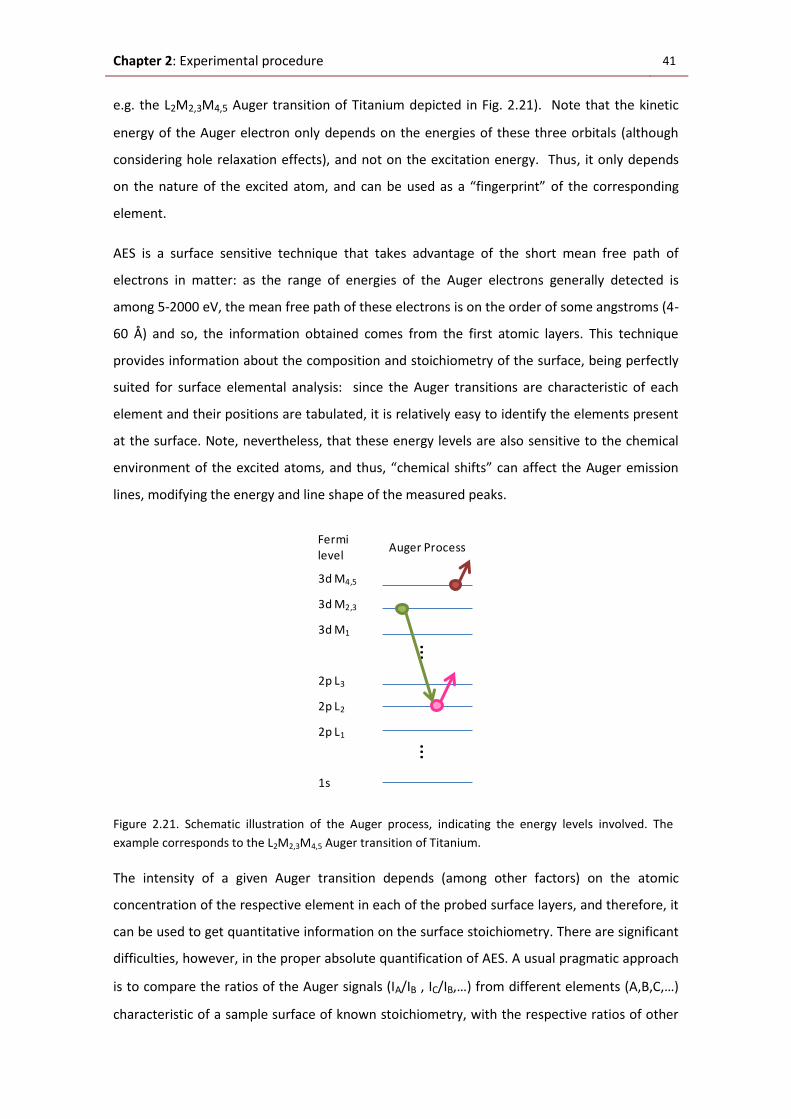
Chapter 2: Experimental procedure 41
e.g. the L2M2,3M4,5 Auger transition of Titanium depicted in Fig. 2.21). Note that the kinetic
energy of the Auger electron only depends on the energies of these three orbitals (although
considering hole relaxation effects), and not on the excitation energy. Thus, it only depends
on the nature of the excited atom, and can be used as a “fingerprint” of the corresponding
element.
AES is a surface sensitive technique that takes advantage of the short mean free path of
electrons in matter: as the range of energies of the Auger electrons generally detected is
among 5-2000 eV, the mean free path of these electrons is on the order of some angstroms (4-
60 Å) and so, the information obtained comes from the first atomic layers. This technique
provides information about the composition and stoichiometry of the surface, being perfectly
suited for surface elemental analysis: since the Auger transitions are characteristic of each
element and their positions are tabulated, it is relatively easy to identify the elements present
at the surface. Note, nevertheless, that these energy levels are also sensitive to the chemical
environment of the excited atoms, and thus, “chemical shifts” can affect the Auger emission
lines, modifying the energy and line shape of the measured peaks.
Figure 2.21. Schematic illustration of the Auger process, indicating the energy levels involved. The
example corresponds to the L2M2,3M4,5 Auger transition of Titanium.
The intensity of a given Auger transition depends (among other factors) on the atomic
concentration of the respective element in each of the probed surface layers, and therefore, it
can be used to get quantitative information on the surface stoichiometry. There are significant
difficulties, however, in the proper absolute quantification of AES. A usual pragmatic approach
is to compare the ratios of the Auger signals (IA/IB , IC/IB,…) from different elements (A,B,C,…)
characteristic of a sample surface of known stoichiometry, with the respective ratios of other
Fermi level
Auger Process
3d M4,5
3d M2,3
3d M1
2p L3
2p L2
2p L1
1s
……

42 2.5. Structural characterization
sample surfaces whose stoichiometry we want to know (measured under similar experimental
conditions). This is the approach used here (see Chapter 5) for the analysis of SrTiO3 surfaces
prepared by different procedures.
The principal disadvantage of AES is that the incident electron beam charges up a non-
conducting sample. This effect, which also affects LEED measurements, may become relevant
in the case of STO surfaces.
The most usual form of measuring and representing AES spectra is that followed here (see e.g.
Fig. 5.15), which involves a differentiation with respect to energy, in order to suppress the
large secondary background on which the Auger signal is mounted, thus emphasizing the
detection of the Auger peaks.
Note that AES and LEED techniques require an ultra-high vacuum (UHV) environment, since
they involve the detection of relatively low energy electrons. In the present case, a commercial
rear view LEED optics (see Fig. 2.22), also adapted for AES mesurements, was available in the
same chamber used for substrate treatments in UHV, and it was employed for the surface
characterization of the STO samples. Auger spectra in the 20 to 550 eV range were taken in the
first derivative mode (dN/dE), using a 2 KeV incident electron beam. Special care was placed to
use the same measurement parameters (emission current, sample to detector distance, peak-
to-peak voltage, amplitude or sensitivity, pass energy, d-well time, etc …) for all the surfaces
under study.
2.5.3. Low energy electron diffraction
Low Energy Electron Diffraction (LEED) is a technique well suited for the determination of the
surface structure of crystalline materials. Surfaces are bombarded with a collimated beam of
low energy electrons (30-500eV). The wave lengths that correspond to those energies are of
the order of the interplanar distances, and their inelastic dispersion cross sections are maxima,
being the electron mean free path in the range of 10-20 Å (i.e., less than 6 atomic layers).
Therefore, the detected diffracted electrons come from the first atomic layers, making LEED a
classic technique for the crystallographic analysis of surfaces.
Figure 2.22 schematizes a conventional LEED system, similar to that used here, where the
sample is placed at the centre of the optic axis. The backscattered electrons are detected by a
fluorescent semispherical screen, generating the diffraction pattern. The LEED detector usually
contains three or four hemispherical concentric grids (used for screening out the inelastically
scattered electrons) and a phosphor screen or other position-sensitive detector.

Chapter 2: Experimental procedure 43
Figure 2.22. Conventional LEED system.
If the incident beam is normal to the sample surface, the pattern observed on the fluorescent
screen is a direct picture of the reciprocal lattice of the surface. The size of the Ewald's sphere
and hence, the number of diffraction spots on the screen is controlled by the incident electron
energy. From the knowledge of the reciprocal lattice, information on the real space lattice can
be derived, at least qualitatively (in terms of the surface periodicity and the point group).
2.6. Ferro-piezo electric characterization: Piezoresponse Force
Microscopy.
Piezoresponse Force Microscopy (PFM) is based on the detection of local vibrations of a
sample induced by an electric field applied between the conductive tip of the scanning force
microscope and the bottom electrode of the sample [35, 36]. The local oscillations of the
sample surface are transmitted to the tip and detected using a usual lock-in technique. The
signal at the lock-in output is denoted piezoresponse signal (PRS) [35]. PFM is the only
available technique suitable for the functional characterization of the nanostructures onto
substrates.
Voltage applied to the tip can be expressed as
𝑉𝑡𝑖𝑝 = 𝑉𝑑𝑐 + 𝑉𝑎𝑐 sin𝜔𝑡 (2.8)
The piezoelectric response of the surface is detected as a first harmonic component of bias-
induced tip deflection:
𝑑 = 𝑑0 + 𝐴 · cos 𝜔𝑡 + 𝜙 (2.9)
Electron gunSample
Fluorescent screen
Electron energyselecting grids
Incident beam
Elastically diffractedelectrons

44 2.6. Ferro-piezoelectric characterization
PFM is carried out in contact mode, under a constrained force. Fig. 2.23 shows the
configuration used in this work. PFM measurements were carried out using the SFM
microscope previously described in section 2.4.5 implemented with a SR7265 DSP lock-in
amplifier (Signal Recovery) and a Agilent 33120 function waveform generator. The AC signal is
applied through the bottom electrode.
Figure 2.23. PFM configuration for the obtaining of PFM images and hysteresis loops.
Conductive commercial Pt/Ir coated tips (Nanosensors) on cantilevers were used to apply an
AC voltage of 1-3V at 50 kHz and 245 kHz. These cantilevers are summarized in Fig. 2.24.
Figure 2.24. Nanosensors probes for the acquisition of PFM images. PPP-CONT tips present a higher
resolution due to the fact that the tip is clearly visible from the top, making more accurate the
positioning of the laser spot onto it.
In PFM, cantilevers not only are the probes to measure the reverse piezoelectric effect but also
act as temporally top electrode for the measurement. When the polarization is parallel to the
applied electric field, the deflection of the cantilever takes place in the out-of-plane direction,
and gives rise to a vertical movement of the laser spot in the photosensitive diode. The in-
plane deflection of the cantilever is due to a polarization perpendicular to the applied field. In
detector
samplesubstrate
Laser beam
V(t)
Lock-in amplifier
Function generator
signal output
feedback
reference
A B
C D
PPP-NCHPt• Pointprobe® Plus - tip• Non-Contact High frequency
• C = 42 N/m, fo = 330 kHz• PtIr5 coated probe
ATEC-EFM• Pointprobe® Plus - tip• Contact Mode
• C = 0.7 N/m, fo = 503 kH

Chapter 2: Experimental procedure 45
this case, a horizontal movement of the laser spot is detected by the photosensitive diode.
When the polarization vector presents both parallel and perpendicular contributions, both the
in-plane and the out-of-plane signals are detected.
When the polarization vector pointing downwards (i.e., c- domains), the application of a
positive tip bias results in the expansion of the sample and bias-induced surface oscillations
are in phase with tip voltage f=0. For polarization pointing up-wards (i.e., c+ domains) f =180°.
In the case of the in-plane response, that is to say, when the response is orthogonal to the
applied field, the application of both positive and negative bias results into a shear movement
of the sample [37]. Fig. 2.25 schematizes these effects as well as the most common case of
polarization that presents both the in-plane and out-of-plane contributions.
Figure 2.25. Scheme of the out-of-plane, in-plane and mixed response of a ferroelectric material when
applying an electric field perpendicular to the surface of the nanostructure [38].
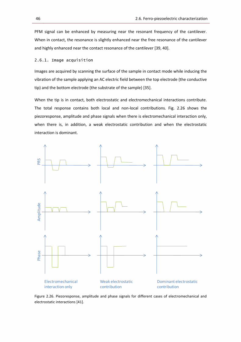
46 2.6. Ferro-piezoelectric characterization
PFM signal can be enhanced by measuring near the resonant frequency of the cantilever.
When in contact, the resonance is slightly enhanced near the free resonance of the cantilever
and highly enhanced near the contact resonance of the cantilever [39, 40].
2.6.1. Image acquisition
Images are acquired by scanning the surface of the sample in contact mode while inducing the
vibration of the sample applying an AC electric field between the top electrode (the conductive
tip) and the bottom electrode (the substrate of the sample) [35].
When the tip is in contact, both electrostatic and electromechanical interactions contribute.
The total response contains both local and non-local contributions. Fig. 2.26 shows the
piezoresponse, amplitude and phase signals when there is electromechanical interaction only,
when there is, in addition, a weak electrostatic contribution and when the electrostatic
interaction is dominant.
Figure 2.26. Piezoresponse, amplitude and phase signals for different cases of electromechanical and
electrostatic interactions [41].
Electromechanicalinteraction only
Weak electrostaticcontribution
Dominant electrostaticcontribution
PR
SA
mp
litu
de
Ph
ase

Chapter 2: Experimental procedure 47
2.6.2. Hysteresis loops.
PFM microscopes can be used in order to obtain local piezoelectric hysteresis loops. There are
two different approaches for obtaining PFM hysteresis loops. In the first one, an increasing
bias is applied in a staircase way, while measuring the PRS or the decoupled amplitude and
phase signals in a stationary state with a small amplitude AC signal. This is called in-field
hysteresis loop (Fig. 2.27 (a)).
In the second type of hysteresis loop, the bias is applied in pulses of increasing or decreasing
value, while the AC electric field is kept constantly on. This kind of hysteresis loops is called
out-of-field or remnant hysteresis loop because the PRS or the decoupled amplitude and phase
signals are measured in the remnant steady state (Fig. 2.27 (b)).
Figure 2.27. Shape of the electric field supplied to the substate for the in-field (a) and out-of -field (b)
local piezoelectric hysteresis loops. AC field is represented in dark red and DC field in green.
a)
b)

48 2.6. Ferro-piezoelectric characterization
Both kinds of hysteresis loops provide complementary information. While the in-field
hysteresis loops shows clearly the electrostatic contribution (as a straight line that passes
through the origin and has a slope proportional to said contribution), the out-of-field ones
provides remnant information.
Measurements are made using the tip of the cantilever as top-electrode. This implies that the
applied field is not uniform with field lines resembling an umbrella. Thus, the measured values
of d33 must be considered as effective values [35].

Bibliography 49
Bibliography
[1] N.J. Phillips, M.L. Calzada and S.J. Milne, "Sol gel-derived lead titanate films", Journal of
non crystaline solids, 147&148, 1992, p:285
[2] R. Sirera, "Síntesis por sol-gel de soluciones de titanato de plomo modificado para la
preparación de láminas delgadas ferroeléctricas", 1997, Madrid: Universidad Autónoma de
Madrid. Ph.D. Thesis.
[3] M. Kawasaki, K. Takahashi, T. Maeda, R. Tsuchiya, M. Shinohara, O. Ishiyama, T.
Yonezawa, M. Yoshimoto and H. Koinuma, "Atomic control of the SrTiO3 crystal-surface",
Science, 266 (5190), 1994, p:1540
[4] T. Ohnishi, K. Shibuya, M. Lippmaa, D. Kobayashi, H. Kumigashira, M. Oshima and H.
Koinuma, "Preparation of thermally stable TiO2-terminated SrTiO3 (100) substrate surfaces",
Applied Physics Letters, 85 (2), 2004, p:272
[5] D.E. Bornside, C.W. Macosko and L.E. Scriven, "On the modeling of spin coating",
Journal of Imaging Technology, 13 (4), 1987, p:122
[6] J.I. Goldstein, D.E. Newbury, P. Echlin, D.C. Joy, C. Friori and E. Lifshin, Scannig Electron
Microscopy and X-ray microanalysis. 1981, New York: Plenum Press.
[7] D.B. Williams and C.B. Carter, Transmision Electron Microscopy. 1996, New York:
Plenum Press.
[8] G. Binnig, C.F. Quate and C. Gerber, "Atomic Force Microscope", Physical Review
Letters, 56, 1986, p:930
[9] S.V. Kalinin, R. Shao and D.A. Bonnell, "Local phenomena in oxides by advanced
scanning probe microscopy ", Journal of the American Ceramic Society, 88 (5), 2005, p:1077
[10] R. Garcia and R. Perez, "Dynamic atomic force microscopy methods", Surface Science
Reports, 47 (6-8), 2002, p:197
[11] P.K. Hansma, J.P. Cleveland, M. Radmacher, D.A. Walters, P.E. Hillner, M. Bezanilla, M.
Fritz, D. Vie, H.G. Hansma, C.B. Prater, J. Massie, L. Fukunaga, J. Gurley and V. Elings, "Tapping
mode atomic-force microscopy in liquids", Applied Physics Letters, 64 (13), 1994, p:1738
[12] C.A.J. Putman, K.O. Vanderwerf, B.G. Degrooth, N.F. Vanhulst and J. Greve, "Tapping
mode atomic-force microscopy in liquid", Applied Physics Letters, 64 (18), 1994, p:2454
[13] Q. Zhong, D. Inniss, K. Kjoller and V.B. Elings, "Fractured polymeric silica fiber surface
studied by tapping mode atomic-force microscopy", Surface Science, 290 (1-2), 1993, p:L688
[14] R.D. Jaggi, A. Franco-Obregon, P. Studerus and K. Ensslin, "Detailed analysis of forces
influencing lateral resolution for Q-control and tapping mode", Applied Physics Letters, 79 (1),
2001, p:135

50 Bibliography
[15] I. Horcas, R. Fernandez, J.M. Gomez-Rodriguez, J. Colchero, J. Gomez-Herrero and A.M.
Baro, "WSXM: A software for scanning probe microscopy and a tool for nanotechnology",
Review of Scientific Instruments, 78 (1), 2007, p:013705
[16] R.E. Blahut, Fast Algorithms for Digital Signal Processing. 1985, New York: Addison-
Wesley.
[17] S.K. Kurtz and F.M.A. Carpay, "Microstructure and normal grain growth in metals and
ceramics. Part II: Experiments", Journal of Applied Physics, 51 (11), 1980, p:5745
[18] J. Ricote and L. Pardo, "Improvement of calcium modified lead titanate piezoceramics
by hot isostatic pressing", Journal of the European Ceramic Society, 20 (11), 2000, p:1677
[19] A. Moure, A. Castro and L. Pardo, "Improvement by recrystallisation of Aurivillius-type
structure piezoceramics from mechanically activated precursors", Acta Materialia, 52, 2004,
p:945
[20] J. Ricote and L. Pardo, "Microstructure-properties relationships in samarium modified
lead titanate piezoceramics--I. Quantitative study of the microstructure", Acta Materialia, 44
(3), 1996, p:1155
[21] J. Ricote, C. Alemany, L. Pardo and C.E. Millar, "Microstructure-properties relationships
in samarium modified lead titanate piezoceramics--II. Dielectric, piezoelectric and mechanical
properties", Acta Materialia, 44 (3), 1996, p:1169
[22] J. Ricote, C. Alemany and L. Pardo, "Microstructural effects on dielectric and
piezoelectric behavior of calcium-modified lead titanate ceramics", Journal of Materials
Research, 10 (12), 1995, p:3194
[23] L. Fuentes, Synchrotron Radiation Diffraction and Scattering in Ferroelectrics, in
Multifunctional polycrystalline ferroelectric materials, L. Pardo and J. Ricote, Editors. in press,
Springer-Verlag
[24] H. Wiedemann, Synchrotron Radiation. 2003, Berlin: Springer-Verlag.
[25] J.D. Bernal, "The structure of graphite", Proceedings of the Royal Society of London
Series a-Containing Papers of a Mathematical and Physical Character, 106 (740), 1924, p:749
[26] P.P. Ewald, "Remark on the work by M Laue - The trinumeric-symmetric x-ray pictures
on regular crystals", Physikalische Zeitschrift, 14, 1913, p:1038
[27] P.P. Ewald, "The theory of the interference of X-rays in crystals", Physikalische
Zeitschrift, 14, 1913, p:465
[28] F.A. Jenkins and H.e. Whtie, Fundamentals of Optics. 1976, Tokyo: Mc Graw-Hill.
[29] B.k. Vainshtein, Modern Crystallography I. 1981, Berlin: Springer-Verlag.
[30] J.K. Cockcroft and A.N. Fitch, Experimental Setups, in Powder Diffraction: Theory and
Practice D. R.E. and S. Billinge, Editors. 2008, The Royal Society of Chemistry: Cambridge.

Bibliography 51
[31] L. Fuentes-Montero, "Software “Anaelu” para Análisis de Patrones Bidimensionales de
Difracción de Rayos X", Fisica de Materiales, 2008, Chihuahua: Centro de Investigacion en
Materiales Avanzados, S. C. Ph.D. Thesis.
[32] L. Fuentes-Montero and L. Fuentes-Cobas. "Modelling of texture effect on 2d
diffraction patterns". in SSRL/LCLS User's conference. 2009. SSRL.
[33] L. Fuentes-Montero, M.E. Montero-Cabrera, L. Calzada, M.P. De la Rosa, O. Raymond,
R. Font, M. Garcia, A. Mehta, M. Torres and L. Fuentes. "Synchrotron Techniques Applied to
Ferroelectrics: Some Representative Cases". in Symposium on Ferroelectricity and
Piezoelectricity held at the 15th International Materials Research Congress (IMRC). 2006.
Cancun, MEXICO.
[34] L. Fuentes, "Anomalous scattering and null-domain ghost corrections for fibre
textures", Textures and Microstructures, 10, 1989, p:347
[35] C. Harnagea, A. Pignolet, M. Alexe and D. Hesse, "Piezoresponse scanning force
microscopy: what quantitative information can we really get out of piezoresponse
measurements on ferroelectric thin films", Integrated Ferroelectrics, 44, 2002, p:113
[36] A. Gruverman, O. Aucello and H. Tokumoto, "Imaging and control of domain structures
in ferroelectric thin films via scanning force microscopy ", Annual review of materials science,
28, 1998, p:101
[37] G. Catalan, B. Noheda, J. McAneney, L.J. Sinnamon and J.M. Gregg, "Strain gradients in
epitaxial ferroelectrics", Physical Review B, 72 (2), 2005, p:020102
[38] A. Rüdinger, S. T., R. A., T. S., S. T. and W. R., "Nanosize ferroelectric oxide - tracking
down the superparaelectric limit", Applied physics A-Materials science & processing, 80 (6),
2005, p:1247
[39] S. Jesse, B. Mirman and S.V. Kalinin, "Resonance enhancement in piezoresponse force
microscopy: Mapping electromechanical activity, contact stiffness, and Q factor", Applied
Physics Letters, 89 (2), 2006,
[40] T. Stoica, R. Calarco, R. Meijers and H. Luth, "Nanoscale imaging of surface
piezoresponse on GaN epitaxial layers", Applied Surface Science, 253 (9), 2007, p:4300
[41] S.V. Kalinin and D.A. Bonnell, Electric scanning probe imaging and modification of
ferroelectric surfaces, in Nanoscale Characterisation of Ferroelectric Materials. Scanning probe
microscopy approach, M. Alexe and A. Gruverman, Editors. 2004, Springer: Berlin. p. 282.


CHAPER 3: FERROELECTRIC NANOSTRUCTURES BY THE
PHENOMENON OF THE MICROSTRUCTURAL
INSTABILITY OF POLYCRYSTALLINE ULTRATHIN FILMS
3.1. The microstructural instability of polycrystalline
ultrathin films
Ultrathin ferroelectric oxide films are those with a thickness below 50 nm [1-3]. They present a
microstructural instability, a phenomenon that makes possible to obtain isolated
nanostructures onto substrates. This effect was first modeled by Lange and co-workers for
epitaxial ultrathin films of PbTiO3 onto SrTiO3 single crystal substrates [4-6].
When the thickness of an ultrathin film is below a critical value, the microstructural instability
causes the film to break into isolated grains in order to lower the free energy of the system, as
explained through the diagram in Fig. 3.1.
CONTINUOUS FILM
Figure 3.1 Spheroidization of a uniform 2-dimensional ultrathin film of initial thickness t and grain size D
(left), as the thermal energy provided to the system increases , and its 3-dimensional analysis (right) [6].
a)
c)
e)
g)
b)
d)
f)
h)

54 3.1. The microstructural instability of polycrystalline ultrathin films
The model film (Fig 3.1 left) is composed of uniform grains of initial grain size D and thickness
t. These grains were allowed to spheroidize at constant volume and the grain centers of mass
are assumed to remain fixed by the substrate. Initially, the configurational change can be
described by the angle between adjacent grains, Ψ, which is allowed to decrease from an
initial value of π degrees. Calculations show that films with an initial D/t ratio less than 8/π will
retain a boundary between the grains even when Ψ decreases to 0 degrees. Films with a D/t
ratio larger than 8/π will, however, reach a point where the grain boundary disappears.
By thermodynamic calculations, Miller et al. [6] demonstrate that the breakup of the ultrathin
film lowers the free energy of the system when the grain-size to film-thickness exceeds a
critical value.
Figure 3.2. Nanoparticles of Pb(Ti, Zr)O3 (PZT) onto SrTiO3 volume distribution [7].
Later on, Dawber et al. [7] and Harnagea et al. [8] prepared ferroelectric nanoislands onto
conductive polycrystalline Si-based substrates. They found that the nanostructures show a
different morphology depending on the sol-gel precursor solution concentration, that is to say,
on the initial thickness and the crystallization temperature [7]. Further studies found that PZT
nanostructures prepared following this procedure do not show single crystal quality [9]. A
scheme of their results is showed in Fig. 3.2.

Chaper 3: Nanoparticles fabrication by the phenomenom of the microstructural instability of polycrystalline ultrathin films
55
Chemical Solution Deposition is a low cost method that enables the preparation of complex
mixed oxide materials supported onto substrates with a well-adjusted stoichiometry. In this
process, the liquid precursors are deposited onto the substrate, obtaining an amorphous
precursor layer that, after thermal treatment leads to a polycrystalline film. This is a powerful
technique for the fabrication of thin and ultrathin films that has been successfully used since
the early 80’s for polycrystalline ferroelectric films.
Using sol-gel, the precursor solution is spun-coated on a substrate to obtain a thin
metalorganic gel layer that subsequently is converted into an amorphous oxide film by a
thermal annealing process. During this thermal treatment of crystallization, depending on film
parameters and annealing conditions, the system transforms either into a continuous ultrathin
film or it patterns itself into nanostructures of a large variety of shapes and sizes. PbTiO3
ultrathin films develop holes during this crystallization process. Upon further annealing, these
holes grow to a stable size, or even cause the film to break up into single crystal islands under
the conditions described previously [9].
This chapter is presented with the aim of a comparative study of the characteristics of the
nanostructures resulting from this procedure and those, original to this thesis, that will be
presented in the following chapters. The crystal structure, microstructure and properties of
the nanostructures prepared from ultrathin films below that critical thickness have been
studied by AFM, SEM, Synchrotron Radiation Diffraction and PFM.
3.2. Nanoscale PbTiO3 structures onto Pt/TiO2/SiO2/(100)Si
substrates prepared by using the phenomenon of the
microstructural instability
The lead titanate precursor solution used in this work has been synthesized by the process
described previously in Chapter 2 (Experimental procedure, Section 2.1.1). In this study,
different sol concentrations are used: 10-1 M, 4·10-2 M, 3·10-2 M, 2·10-2 M, 10-2 M and 5·10-3 M
for the preparation of the nanostructures onto Pt/TiO2/SiO2/(100)Si substrates.
3.2.1. Microscopy and quantitative microstructure analysis
The ultrathin film breaks for a sol dilution below 5·10-3 M when using 1,3-propanodiol as
solvent, as referred in the literature [10, 11]. Sample prepared from the sol dilution 10-1 M is

56 3.2. Nanoscale PbTiO3 structures onto Pt/TiO2/SiO2/(100)Si substrates prepared by using the
phenomenon of the microstructural instability
shown in Fig. 3.3 to illustrate the appearance of a PbTiO3 continuous ultrathin film as seen by
AFM.
Figure 3.3. AFM topography images of a PbTiO3 continuous ultrathin film obtained at different
magnifications: 5x5 µm image (a) and 2x2 µm image (b).
Fig. 3.4 shows the AFM topography images of different samples prepared from sols with
different concentrations, in order to establish the growth mechanism of the particles and for
the sake of comparison with the methods that will follow. For the highest concentration shown
in the figure 4·10-2 M - rounded particles are grown not covering the substrate uniformly. Fig
3.4 (a) shows the topography of this sample at the outer part of the coating, where the
isolated nanostructures can be found. As the concentration decreases (Fig. 3.4 (c)), the
continuous coated area ceases to exist. The particles shape is less rounded, as shown in the
profile plot, with a flat top facet (Fig. 3.4(d)), indicating that the instability phenomenon takes
place throughout the substrate. The resulting structures for a sol with a concentration of
2·10-2 M are needle-shape type that preferentially nucleates around the substrate defects, in
the radial direction. For sol concentrations below 10-2 M, the resulting structures are flat grains
of irregular shape, and lateral dimensions bigger than 200 nm, as shown in the AFM profile
(Fig. 3.4(h)). As in the case of the needles, they preferentially nucleate around the defects.
When the ultrathin film breaks, the resulting particles try to grow with the minimum surface
energy configuration [4-6]. In the case of the PbTiO3 nanostructures onto SrTiO3 single crystal
substrates, this configuration is a pyramid [12], while in the case of PbTiO3 nanostructures
onto Pt/TiO2/SiO2/(100)Si substrates, the minimum surface energy configuration is a rounded
shape [7]. The different shape, which depends on the substrate, is due to the different degree
of mismatch between the lattices of the substrates and that of the nanostructures as well as to
the different relative surface tension values.
1.0µm
21.52 nm
0nm
400nm
8.64 nm
-7.80 nm

Chaper 3: Nanoparticles fabrication by the phenomenom of the microstructural instability of polycrystalline ultrathin films
57
Concentration Topography Profile
4·10-2 M
3·10-2 M
2·10-2 M
10-2 M
5·10-3 M
Figure 3.4 AFM topography images and representative profiles of the PbTiO3 nanostructures onto the
Pt/TiO2/SiO2/(100)Si substrates prepared from sols with different concentrations.
20.92 nm
0.00 nm
400350300250200150100500
8
7
6
5
4
3
2
1
0
X[nm]
Z[n
m]
600nm
38.54 nm
0.00 nm
400350300250200150100500
20
15
10
5
0
X[nm]
Z[n
m]
600nm
27.94 nm
0.00 nm
400350300250200150100500
8
7
6
5
4
3
2
1
0
X[nm]
Z[n
m]
longitudinal direction
transversal direction
600nm
82.48 nm
0.00 nm
400350300250200150100500
35
30
25
20
15
10
5
0
X[nm]
Z[n
m]
600nm
64.90 nm
0.00 nm
400350300250200150100500
15
10
5
0
X[nm]
Z[n
m]
a) b)
c) d)
e) f)
g) h)
i) j)

58 3.2. Nanoscale PbTiO3 structures onto Pt/TiO2/SiO2/(100)Si substrates prepared by using the
phenomenon of the microstructural instability
When decreasing the concentration of the precursor sol to 3·10-2 M, it is observed that some
areas contain isolated particles, which are rounded, and other areas have a group of non
isolated structures that have a flat top facet (Fig. 3.4). If the amount of material is low enough,
the continuity of the ultrathin gel layer will be lost before any thermal treatment is carried out.
One of the parameters that is critical for the evolution of the discontinuity of the films is how
apart are these areas: as they grow, the mass that was initially occupying these areas must be
redistributed, increasing the thickness of the film and, maybe, filling in some other areas. So,
for some areas, the film thickness will be increased dramatically, meaning that the particles
will not be able to complete the isolation and subsequent spheroidization and leading to these
non isolated grains with a flat top facet.
For the sample prepared from the 2·10-2 M diluted sol, there is not enough material to form
the initial amorphous continuous ultrathin film, so precursor drops nucleus of crystallization
will appear on heating and form needles, which is a common crystalline growth habit of PbTiO3
crystals.
Concentration Before the crystallization After the crystallization
4·10-2 M
non homogeneous
3·10-2 M
2·10-2 M
<10-2 M
Figure 3.5. Proposed growth evolution of the particles deposited as the concentration of the solutions
decreases.
When the concentration of the diluted sol is 10-2 M or smaller, all the precursor material will
set around the defects (Figure 3.4). When the samples are crystallized, large and flat grains will
be formed around them by coalescence, giving rise to larger particles, but in a smaller number.
The morphologies of the particles in all four growth stages are summarized in Fig. 3.5.
Substrate
D
t
Ψ
Substrate
D
t
Ψ Ψ
Substrate
θ
Substrate Substrate
Substrate
?
Substrate

Chaper 3: Nanoparticles fabrication by the phenomenom of the microstructural instability of polycrystalline ultrathin films
59
Previous works [7, 8] have been devoted to the growth of nanostructures as a function of the
initial film thickness and the crystallization temperature. The appearance of flat-faceted
structures has been observed [7], as well as the preferential nucleation of lead titanate
particles at the substrate imperfections, such as grain boundaries of polycrystalline Pt-coated
substrates, when the material amount is small enough [13]. However, to the knowledge of this
author, the formation of needles prior to that effect has never been reported, which may be
due to the different morphology of the platinum coating of the substrates used for these
samples and the ones used in the literature: while the ones used for the above samples have
small grains (smaller than the tips of AFM cantilevers) and roughness of about 25-30 nm, the
ones used at the works referred have flat grains of some hundreds of nanometers.
In Section 2.4.6, it was explained how to calculate the average size of a given distribution of
size of an object, <s>, and the standard deviation of a lognormal distribution, σs, from the
fitting of the line obtained at the probability plot of such distribution. Here the size of the
nanostructures can be well defined at high concentrations by the equivalent diameter to their
circular shape, since they have more or less the same dimensions in all directions (Fig. 3.4(a) y
(c)), whereas such a parameter will not be valid for needle-shape particles.
From the AFM images of the samples deposited from the 4·10-2 M and 3·10-2 M diluted sols,
the distribution of the particle size was measured using MIP4 software by Digital Image
Systems. Fig 3.6 shows the equivalent diameter distributions of the nanoparticles as well as
the corresponding probability plots. Both distributions are log-normal and the fitting of their
probabilistic lines is analitically expressed by:
y = -18.88 + 4.85·x R = 0.99 (3.1)
for the nanostructures deposited from the 4·10-2 M sol and
y = -13.49 + 3.52·x R = 0.99 (3.2)
for those deposited from the 3·10-2 M sol.
Following this procedure, the average equivalent diameter of the nanostructures derived from
the 4·10-2 M and 3·10-2 M sols are 50 nm and 48 nm with a standard deviation of 11 nm and 14
nm, respectively.
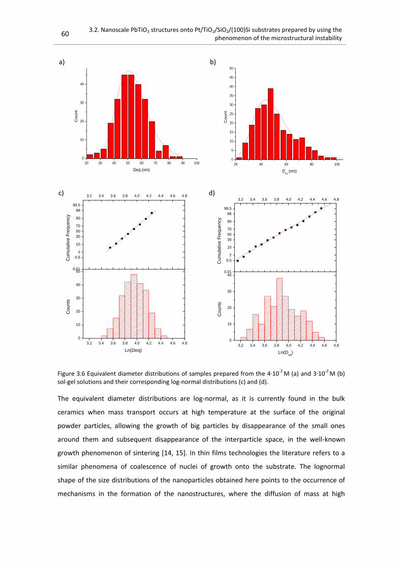
60 3.2. Nanoscale PbTiO3 structures onto Pt/TiO2/SiO2/(100)Si substrates prepared by using the
phenomenon of the microstructural instability
20 30 40 50 60 70 80 90 100
0
10
20
30
40
Co
un
t
Deq (nm)
20 40 60 80 100
0
5
10
15
20
25
30
35
40
45
50
Co
un
t
Deq
(nm)
0,01
0,5
2
10
30
50
70
90
98
99,5
3,2 3,4 3,6 3,8 4,0 4,2 4,4 4,6 4,8
3,2 3,4 3,6 3,8 4,0 4,2 4,4 4,6 4,8
0
10
20
30
40
Co
un
ts
Ln(Deq
)
Cu
mu
lative
Fre
qu
en
cy
Figure 3.6 Equivalent diameter distributions of samples prepared from the 4·10
-2 M (a) and 3·10
-2 M (b)
sol-gel solutions and their corresponding log-normal distributions (c) and (d).
The equivalent diameter distributions are log-normal, as it is currently found in the bulk
ceramics when mass transport occurs at high temperature at the surface of the original
powder particles, allowing the growth of big particles by disappearance of the small ones
around them and subsequent disappearance of the interparticle space, in the well-known
growth phenomenon of sintering [14, 15]. In thin films technologies the literature refers to a
similar phenomena of coalescence of nuclei of growth onto the substrate. The lognormal
shape of the size distributions of the nanoparticles obtained here points to the occurrence of
mechanisms in the formation of the nanostructures, where the diffusion of mass at high
0.01
0.5
2
10
30
50
70
90
98
99.5
3.2 3.4 3.6 3.8 4.0 4.2 4.4 4.6 4.8
3.2 3.4 3.6 3.8 4.0 4.2 4.4 4.6 4.8
0
10
20
30
40
50
Co
un
ts
Ln(Deq)
Cu
mu
lative
Fre
qu
en
cy
c) d)
a) b)

Chaper 3: Nanoparticles fabrication by the phenomenom of the microstructural instability of polycrystalline ultrathin films
61
temperature and coalescence of the structures play an important role during their growth
process.
From the Fig. 3.6 (a) and (b), one can observe how the distribution is becoming more log-
normal and broadening when the concentration of the diluted sol used for these samples
decreases. This behavior has been reported previously [4].
3.2.2. Structural characterization
Fig. 3.7 shows the 2-D diffraction pattern obtained with synchrotron X-ray diffraction in grazing
incidence configuration at the Stanford Synchrotron Radiation Lightsource for the continuous
ultrathin film prepared from the 2·10-2 M sol, using a grazing incidence configuration.
This pattern consists of some sharp rings plus some broad ring portions, located in angle values
close to the said sharp rings (Fig. 3.7 (a)). Furthermore, there are four clear broad spots; three
of them located at the center of the diffraction pattern (indicated by a black point at their
centre) and the fourth on the second quadrant, at low angle positions (Fig. 3.7 (b)).
The integration of the experimental diffraction pattern (as explained in the Experimental
Chapter, 2.5.1.3) is shown in Fig. 3.8. The PbTiO3 perovskite pattern is shown in green and the
integrated pattern is the solid black line. Each peak corresponds to one of the sharp rings or
broad ring portions of the 2-D diffraction pattern of Fig. 3.7. It presents four very intense peaks
as well as some other peaks that are less intense. The simulation of the diffraction pattern for
the crystalline phases present at the sample is shown in colors. The most intense peaks
correspond to the polycrystalline platinum of the substrate (Pt/TiO2/SiO2/(100)Si). The less
intense peaks can be explained by the PbTiO3 perovskite phase. One can observe that the four
most intense peaks have a small contribution of this phase as well. Reflections corresponding
to the PbTiO3 perovskite phase as well as to platinum and titanium oxide are detected in the
diffractogram of Fig. 3.8.
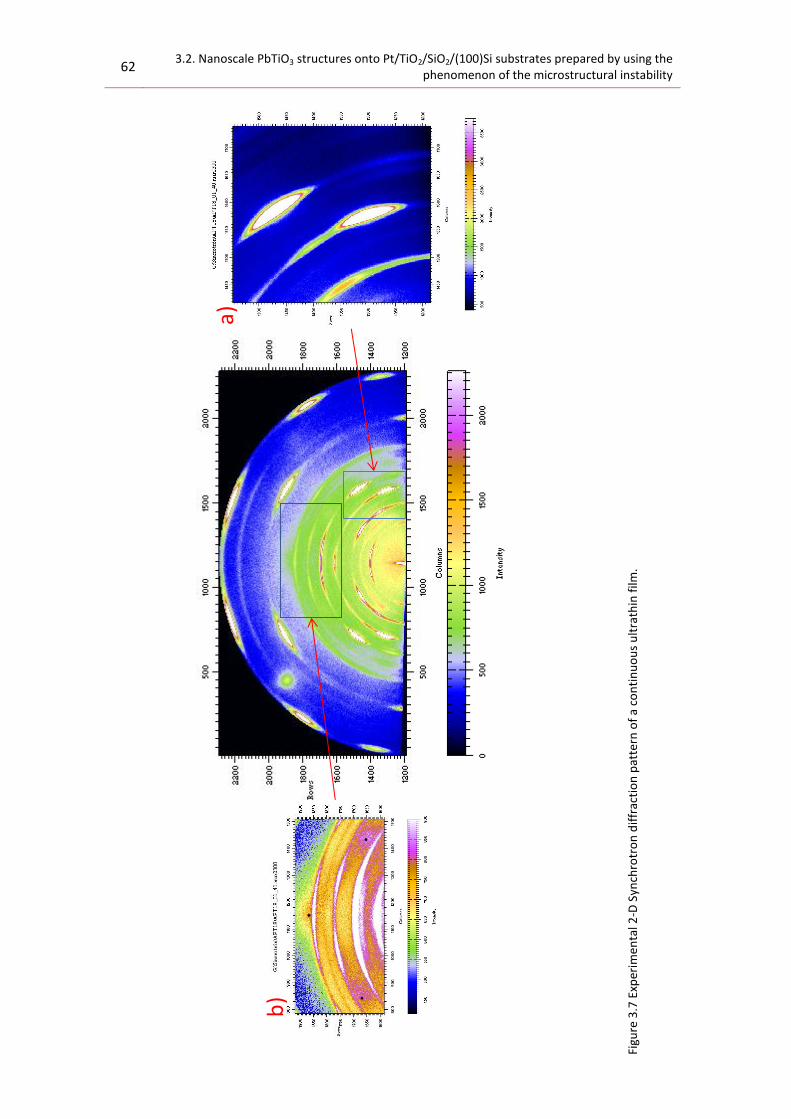
62 3.2. Nanoscale PbTiO3 structures onto Pt/TiO2/SiO2/(100)Si substrates prepared by using the
phenomenon of the microstructural instability
Figu
re 3
.7 E
xper
imen
tal 2
-D S
ynch
rotr
on
dif
frac
tio
n p
atte
rn o
f a
con
tin
uo
us
ult
rath
in f
ilm.
b)
a)
··
·

Chaper 3: Nanoparticles fabrication by the phenomenom of the microstructural instability of polycrystalline ultrathin films
63
Figu
re 3
.8 2
θ d
iffr
acti
on
pat
tern
ob
tain
ed f
rom
th
e in
tegr
atio
n o
f th
e 2
-D e
xper
imen
tal p
atte
rn a
nd
th
e si
mu
late
d d
iffr
acti
on
pat
tern
s o
f th
e P
bTi
O3,
pla
tin
um
,
TiO
2 an
d s
ilico
n o
f th
e su
bst
rate
.
1015
2025
3035
4045
50
3080
422
1540
211
0
Po
wd
er
Ce
ll
2.
2
AN
AT
AS
E 3
.6%
101
103
004
112
200
202
105
211
213
116
220
107
215
301
206
008
303
312
PbTiO3 14.3%
001
100
101
110
111
002
200
102
211
202
003
221
301
Pt 7.1%
111
200
220
311
RUTILE 3.6%
110
101
200
111
220
002
310
212
Si 71.4% (pref.Or)
111
220
222
331
APT18_01_41.X_Y
1015
2025
3035
4045
50
3080
422
1540
211
0
Po
wd
er
Ce
ll
2.
2
AN
AT
AS
E 3
.6%
101
103
004
112
200
202
105
211
213
116
220
107
215
301
206
008
303
312
PbTiO3 14.3%
001
100
101
110
111
002
200
102
211
202
003
221
301Pt 7.1%
111
200
220
311
RUTILE 3.6%
110
101
200
111
220
002
310
212
Si 71.4% (pref.Or)
111
220
222
331
APT18_01_41.X_Y

64 3.2. Nanoscale PbTiO3 structures onto Pt/TiO2/SiO2/(100)Si substrates prepared by using the
phenomenon of the microstructural instability
Figure 3.9-11 shows the more detailed identification of the rings, ring sectors and spots of the
experimental diffractogram shown in Fig. 3.7.
Figure 3.9 Simulated 2-D diffraction pattern of polycrystalline platinum with (111) fiber texture (a) and
the experimental 2-D diffraction pattern measured from the ultrathin film (b).
Figure 3.9 (a) shows the simulated diffraction pattern for a polycrystalline platinum with a
(111) fiber texture with an orientation distribution cone of ±3°, calculated from the inverse
pole figure (see Chapter 2, Experimental Procedure, Section 2.5.1.2, for further explanations).
The intense peak that corresponds to the (331) direction, shown in the simulation by a blue
line over a weak spot.
Figure 3.10 (a) shows the simulated diffraction pattern for (100) Si. It was calculated from the
Inverse Pole Figure. It explains the three interconnected spots at the central part of the
diffractogram, that correspond to the diffraction of the plane families indicated at Fig. 3.10
(a). The lines that interconnect the spots can be understood as diffuse radiation, which is
related to high ordered structures [16] as is the case of the (100)Si wafer. There is another very
intense peak that corresponds to the (331) direction, shown in the simulation by a blue line
over a weak spot.
Figure 3.10 Simulated 2-D diffraction pattern of (100) Si single crystal (a) and the measured 2-D
diffraction pattern from the sample (b). The diffractions maxima that forms the triangle are marked
with a cross (see also Fig. 3.7 (b)).
(311)
(220)
(200)
(111)
a) (311)
(220)
(200)
(111)
b)
a)
(114)
(2-12)(-122)
(331)
(114)
(2-12)(-122)
(331)+
++
b)

Chaper 3: Nanoparticles fabrication by the phenomenom of the microstructural instability of polycrystalline ultrathin films
65
Figu
re 3
.11
Sim
ula
ted
2-D
dif
frac
tio
n p
atte
rn o
f P
bTi
O3
nan
ost
ruct
ure
s w
ith
(1
00
) fi
ber
tex
ture
an
d a
n o
rien
tati
on
dis
trib
uti
on
co
ne
of
±15
° (a
) an
d t
he
mea
sure
d
2-D
dif
frac
tio
n p
atte
rn f
rom
th
e sa
mp
le (
b).
(22
2)
(11
3)
(10
3)
(00
2)
(11
0)
(10
0)
(20
0)
(21
1)
(00
3)
(11
2) (1
11
)
(20
2)
(20
0)
b)
(22
2)
(11
3)
(10
3)
(00
2)
(11
0)
(10
0)
(20
0)
(21
1)
(00
3)
(11
2)
(11
1)
(20
2)
(20
0)
a)b
)

66 3.2. Nanoscale PbTiO3 structures onto Pt/TiO2/SiO2/(100)Si substrates prepared by using the
phenomenon of the microstructural instability
Fig. 3.11 (a) shows the simulated 2-D diffraction pattern of the PbTiO3 perovskite phase,
calculated from the inverse pole figure, considering the lattice parameters to be c = 4.130(1) Å
and a = 3.912(1) Å . The crystalline distortion is c/a = 1.055(7), smaller than the theoretical one
(1.0668) which correspond to a theoretical c = 4.150(0) Å and a = b = 3.890(0) Å. Previous
studies reported the effects of stresses in ferroelectric thin films [17, 18]. They point to three
different reasons for the strains: the different mismatch between substrate and film, the
different thermal expansion of both and the phase transformation of the film with
temperature. The last reason is minimized when cooling down from temperatures above 500
⁰C, which is done in this case. Only lattice and thermal expansion mismatches can result into
strains. There is also another effect that must be considered: the film is subjected to stresses
induced by the substrate [17]. However, this contribution decreases with the thickness of the
film and should be minimized in the case here considered.
All considered, the stresses responsible of the smaller tetragonal distortion found for this thin
film might be mainly due to the different lattice mismatch and thermal expansion of the
PbTiO3 film and the polycrystalline Pt surface.
All the sharp rings not explained yet can be identified by the (100) fiber structures of the
PbTiO3 perovskite phase. Orientation distribution cone is ±15°. Fig. 3.11 indicates to which
family of planes corresponds each ring presented at the diffractogram.
3.2.3. Functional characterization
PFM studies were carried out for the continuous ultrathin film and the isolated nanostructures
prepared from the 10-2 M and 4·10-2 M diluted sol, respectively. Images corresponding to the
amplitude and phase of the piezoresponse of the particles are shown in Fig 3.12 (ultrathin film)
and Fig 3.13 (nanostructures).
The measurements of Fig. 3.12 were performed at the Materials Science Institute of Madrid
under an AC field of amplitude 2V -peak to peak- and a frequency of 50 kHz. The image shows
that almost all grains have a polarization that is not purely in-plane or out-of-plane but rather
have both contributions. There are two areas that present no ferro-piezoresponse: one at the
bottom right part of the image and another one at the centre.

Chaper 3: Nanoparticles fabrication by the phenomenom of the microstructural instability of polycrystalline ultrathin films
67
Figure 3.12. Topography (a) and (d), phase (b) and amplitude (c) images of the in-plane piezoresponse
and phase (e) and amplitude (f) of the out-of-plane piezoresponse for the continuous ultrathin PbTiO3
film.
In the case of the piezoresponse of the nanostructures of Fig. 3.13, the measurements were
carried out at the Max Planck Institute for Microstructure Physics under an AC field of
amplitude 1.5V -peak to peak- and a frequency close to the contact resonance of the cantilever
Figure 3.13. Topography (a), phase (b) and amplitude (c) images of the out-of-plane piezoresponse for
the PbTiO3 nanostructures.
(245kHz), in order to enhance the measurements using the ATEC-EFM cantilevers, as explained
in Chapter 2 (Experimental Procedure, Section 2.6.3).
The image shows different contrast and amplitude at the top facet of the nanostructures than
at the lateral. Most probably, the coating or the cantilever tip is damage and, consequently,
25.46 nm
0nm
PZ
125 pm/V
0.00
PFM Image Amplitude image
PFM Image Phase imageAFM Image
PFM Image Amplitude image
PFM Image Phase imageAFM Image
25.46 nm
0nm
PZ
81pm/V
0.00
25.46 nm
0nm
PZ
0.00
a) b) c)
d) e) f)
PFM Image Amplitude image
PFM Image Phase imageAFM Image
100nm100nm100nm
PZ
18.21 nm
0nm
30 pm/V
0.00
a) b) c)

68 3.2. Nanoscale PbTiO3 structures onto Pt/TiO2/SiO2/(100)Si substrates prepared by using the
phenomenon of the microstructural instability
the response is enhanced when the part of the tip that is not damaged still is in contact with
the nanostructure.
Measurement conditions: Vac = 1.5V
Freq ac = 245kHz F = 25 nN
Tbias = 0.2s Tmeasurement = 0.3s
SEN = 1mV TC = 20 ms
Figure 3.14. Out-of-field consecutive local hysteresis loops of a nanoparticle of 50nm.
Furthermore, the out-of-field consecutive local hysteresis loops of the isolated nanostructures,
shown in Fig. 3.14, verify the ferro-piezoelectric character of these PbTiO3 nanostructures.
Hysteresis loops are asymmetric with respect to the piezoresponse axis. In ferroelectric
nanoparticles, Rodriguez et al. [19] have already found this effect. It is due to a pinned layer at
the bottom part of the nanostructure that clamps the switching of the polarization. The nature
of the pinned layer is unknown, but most probably related with certain crystal structure
defects occurring at the interface between the substrate and the ferroelectric particle (Fig.
3.15). When the field is applied in the same direction as the pinned polarization, its
contribution adds to that switched by the field, whereas when the field is applied in the
opposite polarity this contribution is subtracted from the switched one giving place to the
asymmetry of the loop. The hysteresis loops also present an asymmetry with respect to the
voltage axis which is related to a certain imprint of the nanostructures. This effect is well-
known as it takes place in most thin films [20].
Figure 3.15. Scheme of the pinned layer and the imprint (a) and its effect on a hysteresis loop (b)[21]
-10 -5 0 5 10
-40
-20
0
20
40
60
80
100
Pie
zo
-Re
sp
on
se
(a
.u)
Voltage (V)
1st cycle
2nd cycle
3rd cycle
4th cycle
5th cycle

Chaper 3: Nanoparticles fabrication by the phenomenom of the microstructural instability of polycrystalline ultrathin films
69
Remarks
1. Isolated structures of PbTiO3 onto Pt/TiO2/SiO2/(100)Si substrates prepared by using
the phenomenon of the microstructural instability of polycrystalline ultrathin films
change the shape and size when the sol concentration, and thus the film thickness, is
decreased. Also, nanostructures in the range of the 50 nm are obtained from 4·10-2 M
and 3·10-2 M sols.
2. The equivalent diameter distributions of the nanostructures are log-normal. This
means that the mechanisms of growth involve coalescence and diffusion among
neighbor particles.
3. The amount of structures decreases with the concentration. For sol concentrations
below 3·10-2 M, structure size increases as the sol concentration decreases, up to some
300 nm of lateral dimensions. At 2·10-2 M needle structures are formed. For lower sol
concentration (10-2 M and below), all the structures nucleate and grow around the
defects of the substrate surface.
4. No self-arrangement of the nanostructures is obtained by this procedure onto
Pt/TiO2/SiO2/(100)Si substrates.
5. 2-D synchrotron radiation grazing-incidence diffractograms of a continuous ultrathin
film present reflections corresponding to those of the PbTiO3 perovskite crystal
structure. The orientation of the crystallites is a fiber one with the (100) axis
perpendicular to the surface of the substrate and a direction distribution cone of ±15°.
Cell parameters of the PbTiO3 perovskite deduced from this pattern are c = 4.130(1) Å,
a = 3.912(1) Å.
6. The isolated PbTiO3 nanostructures here grown in the range of the 50 nm show a
ferro-piezoelectric local behavior.

70 Bibliography
Bibliography
[1] G.L. Brennecka, C.M. Parish, B.A. Tuttle, L.N. Brewer and M.A. Rodriguez, "Reversibility
of the perovskite-to-fluorite phase transformation in lead-based thin and ultrathin films",
Advanced materials, 20 (8), 2008, p:1407
[2] G.L. Brennecka, C.M. Parish, B.A. Tuttle, L.N. Brewer and M.A. Rodriguez, "Multilayer
thin and ultrathin film capacitors fabricated by chemical solution deposition", Journal of
Materials Research, 23, 2008, p:176
[3] G.L. Brennecka and B.A. Tuttle, "Fabrication of ultrathin film capacitors by chemical
solution deposition", Journal of Materials Research, 22 (10), 2007, p:2868
[4] A. Seifert, A. Vojta, J.S. Speck and F.F. Lange, "Microstructural instability in single-
crystal thin films", Journal of Material Research, 11 (6), 1996, p:1470
[5] J.H. Kim and F.F. Lange, "Seeded epitaxial growth of PbTiO3 thin films on (001) LaAlO3
using the chemical solution deposition method", Journal of Material Research, 14 (4), 1999,
p:1626
[6] K.T. Miller, F.F. Lange and D.B. Marshall, "The instability of polycrystalline thin films:
Experiment and theory", Journal of Material Research, 5 (1), 1990, p:151
[7] M. Dawber, I. Szafraniak, M. Alexe and J.F. Scott, "Self-patterning of arrays of
ferroelectric capacitors: description by theory of substrate mediated strain interactions",
Journal of Physics: Condensed Matter, 15, 2006, p:L667
[8] C. Harnagea, A. Pignolet, M. Alexe and D. Hesse, "Piezoresponse Scanning Force
Microscopy: What Quantitative Information Can We Really Get Out of Piezoresponse
Measurements on Ferroelectric Thin Films", Integrated Ferroelectrics, 44, 2002, p:113
[9] M. Alexe and D. Hesse, "Self-assembled nanoscale ferroelectrics", Journal of Material
Research, 41, 2006, p:1
[10] J. Ricote, S. Holgado, P. Ramos and M.L. Calzada, "Piezoelectric ultrathin lead titanate
films prepared by deposition of aquo-diol solutions", IEEE Transactions on Ultrasonics
Ferroelectrics and Frequency Control, 53 (12), 2006, p:2299
[11] J. Ricote, S. Holgado, Z. Huang, P. Ramos, R. Fernandez and M.L. Calzada, "Fabrication
of continuous ultrathin ferroelectric films by chemical solution deposition methods", Journal of
Materials Research, 23 (10), 2008, p:2787
[12] I. Szafraniak, C. Harnagea, R. Schloz, S. Bhattacharyya, D. Hesse and M. Alexe,
"Ferroelectric epitaxial nanocrystals obtained by a self-patterning method", Applied Physics
Letters, 83 (11), 2003, p:2211

Bibliography 71
[13] R.W. Schwartz, T. Schneller and R. Waser, "Chemical solution deposition of electronic
oxide films", Comptes Rendus Chimie, 7, 2004, p:433
[14] J.S. Reed, Principles of Ceramic Processing. 2nd ed. 1995, New York: Wiley-Interscience
Publication.
[15] C.S. Pande and S.P. Marsh, "The analytical modeling of normal grain-growth", Jom-
Journal of the Minerals Metals & Materials Society, 44 (9), 1992, p:25-29
[16] P.R. Comès, M. Lambert and A. Guinier, "Désordre Linéaire dans le Cristaux (cas du
Silicium, du Quartz, et des Pérovskites Ferroelectriques).", Acta Crystallographica A26, 1970,
p:244-254
[17] J. Mendiola, M.L. Calzada, P. Ramos, M.J. Martin and F. Agulló-Rueda, "On the effects
of stresses in ferroelectric (Pb, Ca)TiO3 thin films", Thin Solid Films, 315, 1998, p:195-201
[18] G.A.C.M. Spierings, G.J.M. Dormans, W.G.J. Moors, M.J.E. Ulenaers and P.K. Larsen,
"Stresses in Pt/Pb(Zr, Ti)O3/Pt thin-films stacks for integrated ferroelectric capacitors", Journal
of Applied Physics, 78 (3), 1995, p:1926-1933
[19] B.J. Rodriguez, S. Jesse, M. Alexe and S.V. Kalinin, "Spatially Resolved Mapping of
Polarization Switching Behavior in Nanoscale Ferroelectrics", Advanced materials, 20 (15),
2008, p:102
[20] H.N. AlShareef, D. Dimos, W.L. Warren and B.A. Tuttle, "Voltage offsets and imprint
mechanism in SrBi2Ta2O9 thin films", Journal of Applied Physics, 80 (8), 1996, p:4573-4577
[21] C.M.P. G.L. Brennecka, B.A. Tuttle, L.N. Brewer, M.A. Rodriguez, "Multilayer thin and
ultrathin film capacitors fabricated by chemical solution deposition", Journal of Material
Research, 23, 2008, p:176


CHAPTER 4: FERROELECTRIC NANOSTRUCTURES BY
MICROEMULSION MEDIATED SYNTHESIS ONTO
Pt/TiO2/SiO2/(100)Si SUBSTRATES
4.1. The microemulsion mediated synthesis
The term surfactant comes from surface acting agent. A surfactant is an amphiphilic molecule,
that is to say, it has a hydrophilic and a hydrophobic part, which are called “head” and “tail”,
respectively. Because they have these two distinguishable parts, they usually are found at the
interfaces and can be used in a wide range of applications: microemulsions, detergents,
membranes, liquid crystals or liposomes [1].
Surfactants can be divided into anionic, cationic and non-ionic surfactants, depending on the
structure of their head. In this work, a non-ionic molecule will be used: Polyoxyethylene (4)
lauryl ether which chemical formula is CH3-(CH2)10-CH2-(O-CH2-CH2)4-OH and commercial name
is Brij-30. A representation of the molecule is shown in Fig. 4.1.
Figure 4.1. Representation of Brij-30 with the head and tail groups indicated.
If surfactant molecules are added to an emulsion (mixture of two immiscible liquids), they try
to organize in order to minimize the chemical potential, stabilizing the groups of one of the
phases in the other and preventing them from reverting into two different layers.
Emulsions are usually described as water-in-oil and oil-in-water type or direct and inverse
emulsions, respectively, depending on which is the continuous medium. Also, depending on
the size of the non-continuous phase drops, they can be divided in microemulsions,
miniemulsions or emulsions [2, 3].
The shape and size of the colloidal aggregates depend on the type of surfactant and the nature
and relative quantity of the two phases present in the emulsion. Fig. 4.2 shows some of the
possible aggregates.

74 4.1. The microemulsion mediated synthesis
Figure 4.2. Some of the possible colloidal aggregates of surfactant molecules in an emulsion. One of the
phases of the emulsion is presented in light blue and the other one in white. Surfactant head is
represented by a circle and the tail by a line.
One of these possible assemblies are micelles. Micelles are a grouping of surfactant molecules
where either the hydrophobic (in a polar continuous phase) or the hydrophilic (in a non-polar
continuous phase) ends cluster inward to escape the continuous phase, keeping one of the
liquids of the emulsion inside. If the heads form the inside of the aggregate, then it is called an
inverse micelle and in the opposite case, it is called a direct micelle (see Fig. 4.2). Micelles are
formed by the core, a liquid pool inside, and the shell, formed by the surfactant.
In this work, microemulsions will be prepared from a mixture of cyclohexane (as oil), water and
Brij-30. The molar ratio of water/surfactant is kept constant ~1.2, which gives place to inverse
micelles with a spherical shape [4]. Fig. 4.3 schematizes the configuration of the microemulsion.
Surfactant molecule Inverse micelle Direct micelle
Planar lamellar phase Onion like lamelar phase

Chapter 4: Ferroelectric nanostructures by microemulsion mediated synthesis onto Pt/TiO2/SiO2/(100)Si substrates.
75
Figure 4.3. Schema of the inverse micelles inside the microemulsion prepared in this work. Core is
identified as medium blue and shell as dark blue. A detailed image shows the configuration of the
surfactant molecules.
Microemulsion mediated synthesis includes all the approaches that involve the formation of
micelles from a surfactant in a mixture of water and oil. This group of procedures had been
inspired by Nature. The assembly process in biological organization is controlled under
thermodynamic and hydrophobic effects. The hydrophobic effect is a unique organizing force,
based on repulsion by the solvent instead of attractive forces at the site of organization and is
responsible for assembly of membranes of cells [5, 6].
When a microemulsion is added to a sol, sol particles will introduce themselves inside the core
of the micelle, keeping the water content unaltered. This resulting solution will be denoted
hereinafter as micellar solution. In this work, it is hypothesized that these micelles that contain
water and sol particles will be the building units from which the crystalline nanostructures will
be formed.
Fig. 4.4 schematizes the formation of the micellar solution, considering the solvents, sol and
surfactant that will be used in this work. Note that most of the micelles will contain sol
particles inside, but they will be some with only water in their core.

76 4.1. The microemulsion mediated synthesis
Figure 4.4. Schematic formation process of the micellar solution. The dark blue annulus represents the
shell of the micelle and of the building unit.
Further self-organization of micelles into periodic hexagonal, cubic or lamellar phases places
both the organic and inorganic compounds into 3-D arrangements, as a result of hydrophobic
and thermodynamic effects. That makes of the drying step a very important one. Theoretically,
if there is no interaction between the solvent (1,3-propanediol) and the micelles, the liquid
from the pores in between the micelles would evaporate leaving the network exposed.
However, adsorption and capillary forces tend to produce the collapse of the micelles network,
if a controlled drying is not carried out. This also causes solvent to flow from the interior of the
coating in order to replace that liquid that is evaporating. Slow drying process, consequently,
helps to the self-assembly of the micelles (whether with only water at the core, or both water
and sol particles). This is the premise of the evaporation-induced self-assembly process (EISA)
[7, 8], where the drying process is controlled to produce the desired order of the building units
in the coating. In this thesis, this type of drying will be understood as an intermediate step in
the CSD preparation of the self-assembled ferroelectric nanostructures onto substrates. Thus,
1,3-propanediol solvent
H2O
C6H12
O
OO
OOH
O
O
O
O
OH
O
O
O
O
OH
O
O
O
O
OH
O
O
O
O
OH
O
O
O
O
OH
O
O
O
O
OH
O
O
O
O
OH
H2O
H2O
H2O
H2O
1,3-propanediol
H20 + sol
H2O
C6H12 drops
Sol nanoparticles
Microemulsion Sol
Micellar solution

Chapter 4: Ferroelectric nanostructures by microemulsion mediated synthesis onto Pt/TiO2/SiO2/(100)Si substrates.
77
drying times will be long at a low temperature and with a controlled humidity in order to be
under conditions as close as possible to those used in the evaporation-induced self-assembly
process.
Microemulsion mediated synthesis has been extensively used in many different fields [9-17],
and just scarcely in the last two decades for the preparation of perovskite structured
nanocrystalline complex oxides [18-24].
Ferroelectric nanopowders have been prepared by microemulsion mediated synthesis, with
good control of particle size, fully dense and of high purity. In addition, they are processed at
reduced temperatures [18, 22, 24-26], compared with conventional methods of processing of
oxide powders. They have been used as precursors for the conformation and sintering of bulk
ferroelectric ceramics [27]. Ferroelectric thin films onto substrates have also been prepared by
the microemulsion mediated synthesis either by a micellar solution [28] or by adding a certain
amount of surfactant to a precursor sol [29, 30]. Films with a high control of the preferred
orientation and improved ferroelectric properties are obtained.
In particular, their use in the preparation of isolated self-assembled ferroelectric
nanostructures onto substrates has been rarely attempted. One important advantage of this
procedure is that controlled size and shape of the micelles can be achieved, and consequently,
resulting isolated structures would be also obtained with a controlled shape and size.
The work of Bhattacharyya et al. [19] was one of the first attempts to prepare BaTiO3 isolated
nanostructures onto silicon substrates. In order to obtain them, crystalline nanopowders were
prepared from a microemulsion using the procedure established by Herrig and Hempelmann
[22]. These nanopowders were dispersed in an alcohol solvent and the resulting dispersion
deposited afterwards onto a conductive substrate by chemical solution deposition, obtaining
nanostructures with an average size of 50-60 nm. Order of the nanostructures onto the
substrate was not observed and ferroelectric response was not reported.
Grosso et al. [21] chose the di-block copolymer approach, for the preparation of SrTiO3,
MgTa2O6 and CoxTi1-xO2-x nanostructures onto single-crystal Si wafer combining it with dip-
coating process. By this procedure, a low-range hexagonal order of the structures onto the
substrate is obtained. The nanostructures are ~25 nm rounded ones. In this work, the
dielectric characteristics of the SrTiO3 nanoislands were not showed.

78 4.1. The microemulsion mediated synthesis
Kronholz et al. [23] fabricated PbTiO3 nanograins of ~30 nm of lateral size onto predefined TiO2
nanostructures created on Pt/TiO2/SiO2/(100)Si substrates by using a self-organized template
with the aid of PS-b-PVC di-block copolymer micelles. This procedure combines top-down and
bottom-up approaches. This mixed mechanism results into an incipient order of the PbTiO3
nanostructures. Proof of the ferroelectric behaviour of the isolated structures is not reported.
For the development of this work, it is hypothesized that pre-organized templates of inverse
micelles combined with sol-gel synthesis will lead to self-assembled isolated nanostructures
onto substrates with controlled shape and size. In this approach, microemulsion mediated
synthesis will be combined with chemical solution deposition for the preparation of
ferroelectric PbTiO3 isolated nanostructures onto Pt/TiO2/SiO2/(100)Si substrates.
Figure 4.5. Hypothetical self-assembly of the nanostructures: a self-assembly of the micelles (whether
building units or micelles with only water inside) will lead to self-assembly nanostructures after drying
and crystallization. The building units and micelles of the deposited micellar solution are displayed as
violet circles, the micelles with only water inside in blue and the resulting nanoparticles, after thermal
treatment, are represented in orange. A defect in the Pt coating is indicated by a non brown depicted
area.
Pt polycrystalline
TiO2
SiO2
Si wafer
H2OH2O
+ Sol
H2O +
Sol
H2O +
Sol H2O +
SolH2O
H2O +
SolH2O
H2OH2O
+ Sol
H2O
+ Sol
H2O
H2OH2O
+ Sol
H2O
+ Sol
H2O
+ Sol H2O
+ Sol
H2O +
Sol
H2O +
Sol
H2O +
Sol
Drying
Pt coating defect

Chapter 4: Ferroelectric nanostructures by microemulsion mediated synthesis onto Pt/TiO2/SiO2/(100)Si substrates.
79
In addition, micelles may act as nanoreactors, providing an isolated place where the chemical
reactions and synthesis of the compounds might take place [4, 18, 22, 26, 31], helped by the
high pressures inside the core. Thus, the combination of self-assembly ability and the fact that
they work as nanoreactors would turn micelles into the building units for the ferroelectric
nanostructures that will be fabricated in this Chapter.
Thus, the hypothesis is that coating the substrate with the micellar solution will yield self-
assembled nanostructures onto the Pt/TiO2/SiO2/(100)Si substrate. Fig. 4.5 shows a scheme of
the self-assembly process.
Note that not all the micelles will contain sol inside them and, thus, only the previously
denoted as building units will yield oxide nanostructures. This is represented in Fig. 4.5.
As colloids, micellar solutions, microemulsions and sols show the Tyndall effect [32]. This
consists on the light scattering by the colloidal particles or particles in a suspension. When
using a laser beam, a straight line can be seen crossing the colloidal solution (Fig. 4.6). This
qualitative experiment is a proof of the colloidal character of the microemulsion, sol and
micellar solution, prepared in this work.
In order to investigate the size of micelles and sol particles and to unveil the nature of the
particles in the micellar solution, DLS measurements were carried out (Fig. 4.7).
Figure 4.6. Tyndall effect in the microemulsion (a), sol (b) and micellar solution (c)
Sol
b)
Micellar solution
c)
Microemulsion
a)

80 4.1. The microemulsion mediated synthesis
Figure 4.7. DLS measurements for the microemulsion (a), sol (b) and micellar solution (c)
0 200 400 600 800 1000
0,0
0,2
0,4
0,6
0,8
1,0
Norm
alis
ed
inte
nsi
ty
Hydrodynamic radius (nm)
Microemulsiona)
0 10 20 30 40
0,0
0,2
0,4
0,6
0,8
1,0
No
rma
lise
d in
ten
sity
Hydrodynamic radius (nm)
Solb)
0 200 400 600 800 1000
0,0
0,2
0,4
0,6
0,8
1,0
No
rma
lised
inte
nsi
ty
Hydrodynamic radius (nm)
Micellar solutionc)

Chapter 4: Ferroelectric nanostructures by microemulsion mediated synthesis onto Pt/TiO2/SiO2/(100)Si substrates.
81
From these measurements, it was found that micelles formed by Brij-30 have an average
radius of ~275 nm in the microemulsion, while the sol nanoparticles are ~12 nm. The particles
in the micellar solutions have an average radius of ~290 nm. The fact that no particle of ~12nm
is observed in the DLS measurements carried out in the micellar solution indicates that all sol
particles are incorporated into the core of the micelles, protected by the surfactant, in this
micellar solution, as it is needed to give place to isolated nanostructures. Also, we can observe
a slight increment in the radius of the micelles when the sol is set inside, as we would expect. It
is a well-known fact that a change in the viscosity of the core of a micelle with respect to the
solvent one will change its radius and adding sol nanoparticles to the water pool will change
the viscosity of the core [33].
4.2. Nanoscale PbTiO3 ferroelectric structures onto
Pt/TiO2/SiO2/(100)Si substrates prepared by microemulsion mediated
synthesis.
Micellar solution with building units of ~290 nm of average size will be used as precursor
solutions for the preparation of the lead titanate nanostructures onto a conductive coated Si-
wafer. This method is compatible with the silicon technology, and will make these
nanostructures suitable for their use as NV-FeRAM.
4.2.1. Microscopy and quantitative microstructure analysis.
Coatings of the substrate obtained by the deposition of the micellar solutions are not uniform.
The deficient wetting of the substrate by the micellar layer gives place to uncoated areas of
the substrate and coated ones with a thickness gradient. To the naked eye, it can be
distinguished in the coated substrate, after drying and crystallization, a large brown area with
an irregular shape located at the centre of the substrate with a darker boundary, while the
outer part of the substrate remains uncovered (see Fig. 4.8 (a)). Fig. 4.8 (b) shows a
micrograph of the limit of the brown area, where the darker colour is found. Lead titanate
nanostructures correspond to the brighter spots, while the darker scratches on the substrate
reveal the TiO2 underlying stratum of the substrate.
Fig. 4.9 displays the AFM images of samples prepared from the 10-2 M and 5·10-3 M micellar
solutions, taken at the central brown area and at the outer part, close to the edge of this
brown area shown in Fig. 4.8 (a). Fig. 4.9 (a) shows a continuous film that leads to isolated
structures when the coating is thin enough (outer part, Fig. 4.9 (b)). This film can be compared
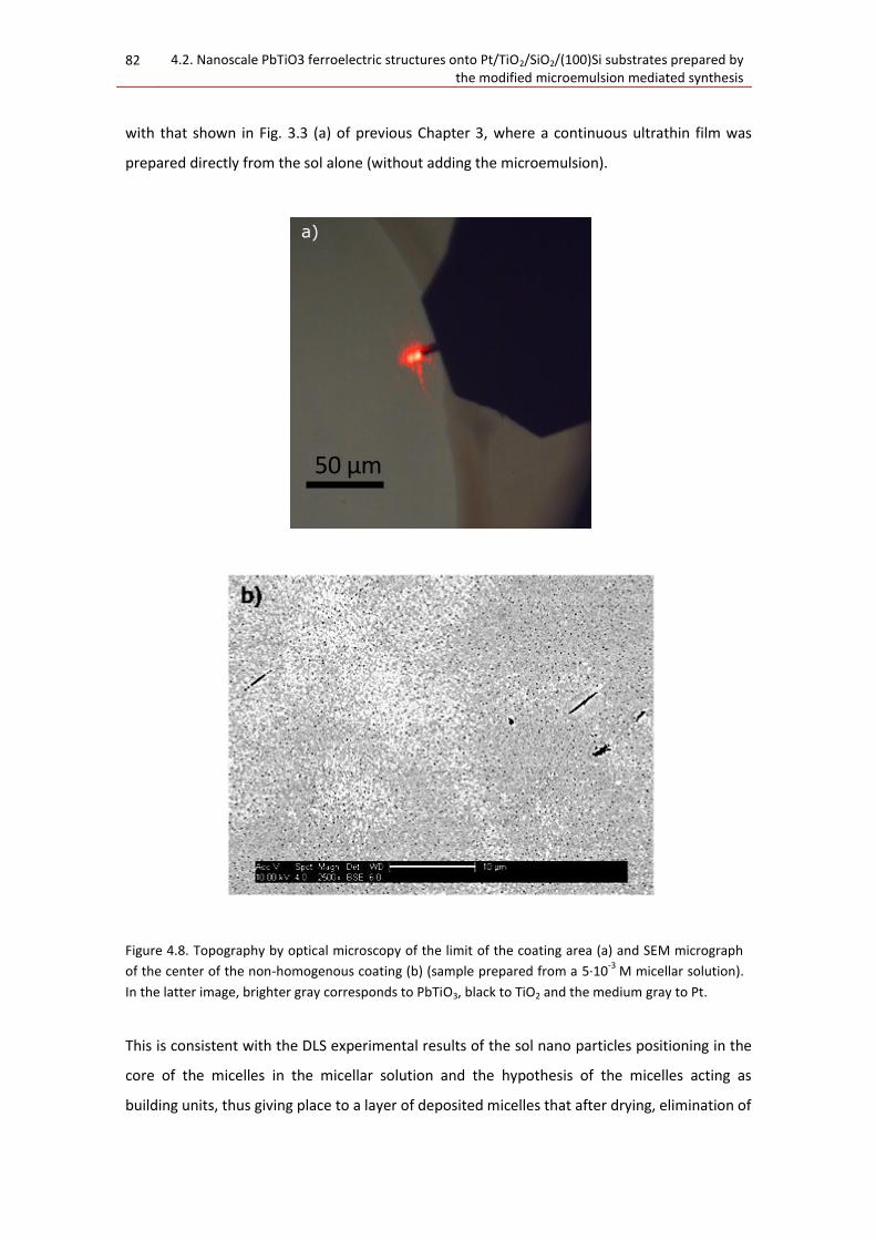
82 4.2. Nanoscale PbTiO3 ferroelectric structures onto Pt/TiO2/SiO2/(100)Si substrates prepared by the modified microemulsion mediated synthesis
with that shown in Fig. 3.3 (a) of previous Chapter 3, where a continuous ultrathin film was
prepared directly from the sol alone (without adding the microemulsion).
Figure 4.8. Topography by optical microscopy of the limit of the coating area (a) and SEM micrograph
of the center of the non-homogenous coating (b) (sample prepared from a 5·10-3
M micellar solution).
In the latter image, brighter gray corresponds to PbTiO3, black to TiO2 and the medium gray to Pt.
This is consistent with the DLS experimental results of the sol nano particles positioning in the
core of the micelles in the micellar solution and the hypothesis of the micelles acting as
building units, thus giving place to a layer of deposited micelles that after drying, elimination of
a)
50 µm

Chapter 4: Ferroelectric nanostructures by microemulsion mediated synthesis onto Pt/TiO2/SiO2/(100)Si substrates.
83
Fi
g. 4
. 9
. A
FM t
op
ogr
aph
y im
age
s o
f th
e P
bTi
O3 n
ano
stru
ctu
res
on
to P
t/Ti
O2/S
iO2/
(10
0)S
i su
bst
rate
s p
rep
ared
fro
m t
he
mic
ella
r so
luti
on
s w
ith
a s
ol
con
cen
trat
ion
of
10
-2 M
(a-
b)
and
5·1
0-3
M (
c) a
t d
iffe
ren
t lo
cati
on
s o
f th
e co
ated
su
bst
rate
.
Co
nc
0.0
1M
y 0
.005
M
Dis
tan
ceto
the
cen
ter
of
the
sub
stra
ted
= 0
64
.08
nm
0n
m
60
.00
nm
0n
m
55
.62
nm
0n
m
a)b
)
c)

84 4.2. Nanoscale PbTiO3 ferroelectric structures onto Pt/TiO2/SiO2/(100)Si substrates prepared by the modified microemulsion mediated synthesis
organics, and crystallization give place to isolated smaller structures than those obtained when
the deposited sol-gel coating breaks due to the phenomenon of the microstructural instability.
If the microemulsion is not used, the deposited sol would crystallize in flat structures of
irregular shape, and lateral dimensions bigger than 200 nm (as explained in Chapter 3, section
3.2.1, Fig. 3.4 (g) and (i)). That is to say, instead of having free precursor particles that will set
around the defects, building units will be distributed uniformly onto the substrate, carrying the
precursor material in their inside from which the oxide nanostructures will be formed.
Figure 4.10. High magnification AFM image of isolated nanostructures fabricated from the 5·10-3
M
micellar solution. The profile of each nanostructure that corresponds to the light violet line is
represented underneath them.
Fig. 4.9 (b) and (c) show nanostructures of similar shape and size. Only their amount on the
surface differs, decreasing with the concentration of the micellar solution. The number of
micelles in the coating layer depends on the amount of water and surfactant in the
microemulsion and, thus in the micellar solution. However, the number of building units with
precursor particles inside depends on the concentration of the sol. Consequently, decreasing
the concentration of the sol leads to a reduced number of crystalline nanostructures onto the
substrate.
The observed nanostructures seem to be formed by coalescence of smaller primary ones. This
can be deduced from the high magnification topography image of Fig. 4.10, where some of the
nanostructures show an imperfect spherical shape that would correspond to the merged of
primary ones. These primary nanostructures would be those resulting from crystallization from
the building units. The characteristic dimensions of the entrapped sol dropplets would be
determined by the physico-chemistry of the microemulsion and, in turn, will determine the
21
150100500
20
15
10
5
0
-5
X[nm]
Z[n
m]
250200150100500
25
20
15
10
5
0
-5
X[nm]
Z[n
m]

Chapter 4: Ferroelectric nanostructures by microemulsion mediated synthesis onto Pt/TiO2/SiO2/(100)Si substrates.
85
Figure 4.11. Proposed drying evolution with time of the micellar layer (a, b) and oxide nanostructures
formed after the thermal treatment of crystallization (c).
H2O
Pt polycrystalline
TiO2
SiO2
Si wafer
H2O +
Sol
H2O + Sol 1,3-propanediol
H2O +
Sol
H2OH2O +
Sol
H2O + Sol
H2O +
Sol
Drying
Thermaltreatment
Capillary forces
Pt coating defects
a)
b)
c)

86 4.2. Nanoscale PbTiO3 ferroelectric structures onto Pt/TiO2/SiO2/(100)Si substrates prepared by the modified microemulsion mediated synthesis
size of the primary nanostructures. Contrary to this, the size of the nanostructures here
observed will depend on the homogeneity of the coating on the substrate and on the
arrangement of the micelles, which ultimately will determine how close the building units and,
subsequently, the merging primary nanostructures are. We can understand this as the result of
inhomogeneity that the surface of the polycrystalline Pt substrate presents and the thickness
of the coating which is not a monolayer of micelles. The deposited micelles tend to
concentrate in certain points during the long process of drying and shrinkage of the coating,
when the solvent is eliminated, leading, during the thermal treatment, to a coalescence of the
primary nanostructures. These nanostructures are not periodically arranged onto the substrate
(Fig. 4.9). In addition to the substrate surface inhomogeneity, there is a second effect that
must be taken into consideration: the deficient wetting of the substrate by the micellar
solution that is partially responsible of the large shrinkage of the coating during the drying step
[34], leading to the collapse of the micelles at the centre of the substrate and yielding the
brown area described before (see Fig. 4.8 (a)).
Fig. 4.11 describes the proposed drying and crystallization processes. As explained in the
introductory part of this Chapter (section 4.1), during drying, adsorption and capillary forces
oppose to the exposure of the micelle network [34]. This will make the micelles and building
units to become closer (Fig. 4.11 (b)) and will finally make a number of primary nanostructures
to be close enough (Fig. 4.11) to coalescence during the thermal treatment and, thus, yielding
a single nanostructure after that (Fig. 4.11 (c)).
Figure 4.12 Equivalent diameter distributions of nanostructures prepared from the 10-2
M (a) and 5·10-
3 M (b) micellar solution.
0.01
0.5
2
10
30
50
70
90
98
99.5
0 20 40 60 80 100 120 140
0 20 40 60 80 100 120 140
0
10
20
30
40
50
Co
un
ts
Deq
(nm)
Cu
mu
lative
fre
qu
en
cy
0,01
0,5
2
10
30
50
70
90
98
99,5
0 20 40 60 80 100 120 140
0 20 40 60 80 100 120 140
0
10
20
30
40
50
Co
un
ts
Deq
(nm)
Cu
mu
lative
fre
qu
en
cy

Chapter 4: Ferroelectric nanostructures by microemulsion mediated synthesis onto Pt/TiO2/SiO2/(100)Si substrates.
87
Fig. 4.12 presents the size distributions of the nanostructures prepared from the 10-2 M and
5·10-3 M micellar solutions, calculated from the AFM images (Fig. 4.9 (b) and (c)).
Both distributions are Gaussian and the fitting of their probabilistic lines is analitically
expressed by:
y = -3.48 + 0.05·x R = 0.99 (3.1)
for the nanostructures deposited from the 10-2 M sol and
y = -3.70 + 0.06·x R = 0.99 (3.2)
for those deposited from the 5·10-3 M sol.
Following this procedure, the average equivalent diameter of the nanostructures derived from
the 10-2 M and 5·10-3 M sols are 75 nm and 67 nm with a standard deviation of 21 nm and 18
nm, respectively.
The fact that both distributions are Gaussian means that the formation of the nanostructures
does not take place via a normal grain growth, which would give place to lognormal
distributions as those measured for nanostructures obtained using the phenomenon of the
microstructural instability of ultrathin films (see Chapter 3, Fig. 3.6). Rather, the
nanostructures grow from independent nucleation points, either isolated building units or
groups of these. As it has been explained for other systems, micelles may act as nanoreactors
[35-38] and so, hydrolysis and crystallization may occur in the core, at least partly, even before
the thermal treatment takes place.
Primary oxide nanostructures could be formed inside the micelles prior to the so-called
thermal treatment. During such thermal treatment, merging between the primary
nanostructures occurs, as revealed by the AFM images of Fig. 4.10, via the usual thermally
stimulated mass transport (diffusion) at the nanostructure surfaces.
4.2.2. Structural characterization
Experiments of synchrotron X-ray diffraction using a 2-dimensional detector were carried out.
Fig. 4.13 shows the resulting pattern of the sample prepared from the 5·10-3 M micellar
solution. It consists of three spots forming a triangle, some broad spots (one of them circular,
the others oval type) and some sharp rings or circular sectors of lower intensity.

88 4.2. Nanoscale PbTiO3 ferroelectric structures onto Pt/TiO2/SiO2/(100)Si substrates prepared by the modified microemulsion mediated synthesis
Figu
re 4
.13
. Exp
erim
enta
l 2-D
syn
chro
tro
n x
-ray
dif
frac
tio
n p
atte
rn o
f a
sam
ple
pre
par
ed f
rom
a 5
·10
-3 M
mic
ella
r so
luti
on
.

Chapter 4: Ferroelectric nanostructures by microemulsion mediated synthesis onto Pt/TiO2/SiO2/(100)Si substrates.
89
Figu
re 4
.14
. 2
θ d
iffr
acti
on
pat
tern
cal
cula
ted
fro
m t
he
inte
grat
ion
of
the
2-D
exp
erim
enta
l pat
tern
of
Fig.
4.1
3 (
bla
ck s
olid
lin
e) a
nd
sim
ula
ted
dif
frac
tio
n p
atte
rns
of
the
Pb
TiO
3 p
ero
vski
te n
ano
stru
ctu
res
(red
lin
e), P
t b
ott
om
ele
ctro
de
(blu
e lin
e), T
iO2
anat
ase
(gr
een
lin
e)
and
Al h
old
er (
ora
nge
lin
e).
15
20
25
30
35
40
45
50
354
177
0
PbT
iO3 32.3
%
001
100
101
110
111
002
200
102
201
112
211
202
003
212
221103
301310
311
222
Al 32.3%
111
200
220
311
222Pt 3.2%
111
200
220
311RUTILE 32.3%
110
101
200
111
210
211
220
002
310
221
301
112
311
320
202
212
400
5PHI000-PHI020-STPW002-5mins_01_03.X_Y
Intensity (a.u.)
2θ
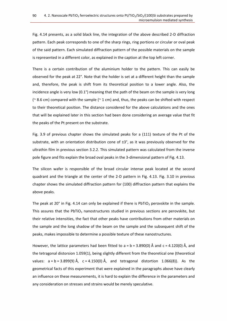
90 4. 2. Nanoscale PbTiO3 ferroelectric structures onto Pt/TiO2/SiO2/(100)Si substrates prepared by microemulsion mediated synthesis
Fig. 4.14 presents, as a solid black line, the integration of the above described 2-D diffraction
pattern. Each peak corresponds to one of the sharp rings, ring portions or circular or oval peak
of the said pattern. Each simulated diffraction pattern of the possible materials on the sample
is represented in a different color, as explained in the caption at the top left corner.
There is a certain contribution of the aluminium holder to the pattern. This can easily be
observed for the peak at 22°. Note that the holder is set at a different height than the sample
and, therefore, the peak is shift from its theoretical position to a lower angle. Also, the
incidence angle is very low (0.1°) meaning that the path of the beam on the sample is very long
(~ 8.6 cm) compared with the sample (~ 1 cm) and, thus, the peaks can be shifted with respect
to their theoretical position. The distance considered for the above calculations and the ones
that will be explained later in this section had been done considering an average value that fit
the peaks of the Pt present on the substrate.
Fig. 3.9 of previous chapter shows the simulated peaks for a (111) texture of the Pt of the
substrate, with an orientation distribution cone of ±3°, as it was previously observed for the
ultrathin film in previous section 3.2.2. This simulated pattern was calculated from the inverse
pole figure and fits explain the broad oval peaks in the 3-dimensional pattern of Fig. 4.13.
The silicon wafer is responsible of the broad circular intense peak located at the second
quadrant and the triangle at the center of the 2-D pattern in Fig. 4.13. Fig. 3.10 in previous
chapter shows the simulated diffraction pattern for (100) diffraction pattern that explains the
above peaks.
The peak at 20° in Fig. 4.14 can only be explained if there is PbTiO3 perovskite in the sample.
This assures that the PbTiO3 nanostructures studied in previous sections are perovskite, but
their relative intensities, the fact that other peaks have contributions from other materials on
the sample and the long shadow of the beam on the sample and the subsequent shift of the
peaks, makes impossible to determine a possible texture of these nanostructures.
However, the lattice parameters had been fitted to a = b = 3.890(0) Å and c = 4.120(0) Å, and
the tetragonal distorsion 1.059(1), being slightly different from the theoretical one (theoretical
values: a = b = 3.899(9) Å, c = 4.150(0) Å, and tetragonal distortion 1.066(8)). As the
geometrical facts of this experiment that were explained in the paragraphs above have clearly
an influence on these measurements, it is hard to explain the difference in the parameters and
any consideration on stresses and strains would be merely speculative.

Chapter 4: Ferroelectric nanostructures by microemulsion mediated synthesis onto Pt/TiO2/SiO2/(100)Si substrates.
91
4.2.3. Functional characterization
Samples prepared from the 10-2 M and 5·10-3 M micellar solutions exhibit local ferro-
piezoelectric local behaviour as displayed in the PFM images of Figs. 4.15-17 and the hysteresis
loops shown in Fig. 4.18. The measurements were performed for an AC frequency close to the
free resonance frequency of the cantilever in order to enhance the signal obtained (see section
2.6 for further explanation).
Fig. 4.15 shows the in-plane and out-of plane piezoresponse images, together with the
corresponding AFM topography images for the same area of the sample prepared from the 10-
2 M micellar solution. It displays areas of agglomerated nanostructures that show a clear ferro-
piezoresponse. The polarization vector has both the in-plane and the out-of-plane components,
although the perpendicular to the surface is stronger (scales for the amplitude are the same
for both types of signals). There are also two single isolated nanostructures (marked with a
black point (·)) that exhibit a ferro-piezoelectric behaviour also with both the in-plane and out-
of plane components. A detailed observation of Fig. 4.15 (f) reveals lighter areas that
correspond to the non-agglomerated nanostructures of Fig. 4.15 (d). Although they are weaker
than the one for the agglomerates, it means that there is a mechanical displacement of the
cantilever and, thus, a ferro-piezoelectric response also in isolated nanostructures.
Fig. 4.16 displays the topography and corresponding out-of-plane response of isolated
nanostructures fabricated from the 5·10-3 M micellar solution. Only out-of-plane response was
found. All of the nanostructures distinguishable at the topography image (Fig. 4.16 (a)) exhibit
ferro-piezoelectric response. Pt is a conductive layer and so, the electrostatic contribution is
not zero but a constant value greater than the amplitude of the piezoresponse of the
nanostructures [39], explaining the inverse contrast observed at image (c) of Fig. 4.16.
Fig. 4.17 shows the topography, phase and amplitude image of an isolated nanostructure
fabricated from the 5·10-3 M micellar solution with domains inside. Domains can be found at
the largest nanostructures and their width is 20-30 nm, approximately.
Out-of-field piezoresponse hysteresis loops for an AC voltage at the free resonance of the
cantilever (Fig. 4.18 (a) and (b)) and at its contact resonance (Fig. 4.18 (c)) have been measured
at an isolated nanostructure of ~93 nm and ~83 nm of lateral size, respectively, from the

92 4. 2. Nanoscale PbTiO3 ferroelectric structures onto Pt/TiO2/SiO2/(100)Si substrates prepared by microemulsion mediated synthesis
.
Figu
re 4
.15
. To
po
grap
hy
(a)
and
(d
), p
has
e (b
) an
d (
e) a
nd
am
plit
ud
e (c
) an
d (
f) im
age
s o
f th
e in
-pla
ne
and
ou
t-o
f-p
lan
e p
iezo
resp
on
se,
resp
ect
ivel
y, f
or
a sa
mp
le p
rep
ared
fro
m t
he
mic
ella
r so
luti
on
wit
h a
10
-2 M
co
nce
ntr
atio
n.
PZ
40
.81
nm
0n
m
31
pm
/V
0.0
0
PZ
40
.81
nm
0n
m
31
pm
/V
0.0
0
PFM
Im
age
Am
plit
ude im
age
PFM
Im
age
Phase im
age
AFM
Im
age
Out-
of-
pla
ne
In-p
lane
a)
b)
c)
d)
e)
f)

Chapter 4: Ferroelectric nanostructures by microemulsion mediated synthesis onto Pt/TiO2/SiO2/(100)Si substrates.
93
Fig
ure
4.1
6.
Top
ogr
aph
y (a
), p
has
e (b
) an
d a
mp
litu
de
(c)
ou
t-o
f-p
lan
e p
iezo
resp
on
se i
mag
es
for
the
iso
late
d n
ano
stru
ctu
res
of
a sa
mp
le p
rep
ared
fro
m t
he
mic
ella
r
solu
tio
n w
ith
a 5
·10
-3 M
co
nce
ntr
atio
n.
19
.46
nm
-6.2
1 n
m
PZ
1.4
5 p
m/V
0.0
0
20
0nm
a)
200nm
c)
20
0nm
b)
b)
Out-
of-
pla
ne
PFM
Im
age
Am
plit
ude im
age
PFM
Im
age
Phase im
age
AFM
Im
age

94 4. 2. Nanoscale PbTiO3 ferroelectric structures onto Pt/TiO2/SiO2/(100)Si substrates prepared by microemulsion mediated synthesis
Figu
re 4
.17
. To
po
grap
hy
(a),
ph
ase
(b)
and
am
plit
ud
e (c
) im
ages
of
the
do
mai
n s
tru
ctu
re o
f a
big
nan
ost
ruct
ure
(~2
00
nm
of
late
ral s
ize)
.
19
.46
nm
-6.2
1 n
m
PZ
1.4
5 p
m/V
0.0
0
a)
c)
b)
Out-
of-
pla
ne
PFM
Im
age
Am
plit
ude im
age
PFM
Im
age
Phase im
age
AFM
Im
age
25
02
00
15
01
00
50
0
5 4 3 2 1 0
X[n
m]
Z[µm]e)
d)

Chapter 4: Ferroelectric nanostructures by microemulsion mediated synthesis onto Pt/TiO2/SiO2/(100)Si substrates.
95
sample prepared from the 5·10-3 M micellar solution. As expected, piezoresponse is enhanced
when measuring with an AC field close to the contact resonance of the cantilever [40].
Hysteresis loops are symmetric with respect to the voltage axis as well as to the piezoresponse
axis. This is in contrast to the results obtained previously in Chapter 3, showed in Fig. 3.15,
where an isolated nanostructure of 50 nm of lateral size presented an asymmetric hysteresis
loop with respect to both axes.
Measurement conditions:
Vac = 1.0 V, Freq = 65 kHz, F = 100nN, Tbias = 0.1s, Tmeasurement = 4.5s, SEN = 5mV,
TC = 10 ms
Measurement conditions:
Vac=1.5V
Freq= 245 kHz
F= 25nN
Tbias= 0.2s
Tmeasurement= 0.3s
SEN = 5mV
TC= 20 ms
Figure 4.18. Out-of-field local hysteresis loops of isolated nanostructures of ~95 nm of lateral size(phase
(a) and amplitude (b) loops) and ~83 nm of lateral size(c) (four consecutive piezoresponse loops)
isolated nanostructures fabricated from the 5·10-3
M micellar solution.
-10 -5 0 5 10-200
-150
-100
-50
0
50
100
150
200
Phase (
º)
Voltage (V)
-10 -5 0 5 10
-1,5
-1,0
-0,5
0,0
0,5
1,0
1,5
d3
3
eff(p
m/V
)
Voltage (V)
a) b)
-8 -6 -4 -2 0 2 4 6 8
-1000
-800
-600
-400
-200
0
200
400
600
800
1000
1200
Pie
zo
resp
on
se
(a
.u.)
Voltage (V)
c)

96 4. 2. Nanoscale PbTiO3 ferroelectric structures onto Pt/TiO2/SiO2/(100)Si substrates prepared by microemulsion mediated synthesis
In Fig. 4.18 (c), the first hysteresis loop measured is different from the subsequent ones. It is
symmetric with respect to both the voltage and piezoresponse axis while the next ones are not,
becoming more asymmetric with respect to the piezoresponse axis. It can be attributed to an
imprint [41] that becomes more relevant as the nanostructure suffers subsequent loops.
On the other hand, the area over the voltage axis becomes smaller, while the one underneath
remains less altered. The nanostructures have an initial polarization that can be attributed to
the condition of the ferroelectric/metallic interface of the substrate. As the voltage field
increases, the polarization reverses, reaching the saturation voltage. Subsequently, the voltage
field decreases, until it becomes negative. In this step, a certain clamped volume is formed,
with the polarization set in the same direction as it was initially. When the field is in the
opposite direction and big enough to make the polarization switch, this clamped polarized
layer will stay unaltered, decreasing the piezoresponse in only one direction.
Figure 4.19 Proposed switching mechanism for the isolated nanostructures.
Fig. 4.19 shows a schematic drawing of the proposed mechanism of switching at the
nanostructures, being (a) the first hysteresis loop and (b) the second one. Hysteresis loop (a)
has initial polarization of unknown nature but that should be compensated by charges on the
surface. When an external electric field is applied, two effects take place. On one hand,
Schottky barrier formed at the metal-ferroelectric junction will decrease. Typically,
ferroelectric titanates present a region near the interface ferroelectric/metal more oxygen
deficient than the inside, creating a gradient of oxygen vacancies and causing the interface to
be slighter p-type than the inside. This makes the energy band to bend as shown in Fig. 4.20
and enables a charge injection towards the ferroelectric nanostructure [42].
-12 -10 -8 -6 -4 -2 0 2 4 6 8 10 12
-1400
-1200
-1000
-800
-600
-400
-200
0
200
400
600
800
1000
1200
1400
Pie
zo
resp
on
se
(a
.u.)
Voltage (V)
+ + + + + +
Substrate
P+ + + + + +
Substrate
+ + + + + +
Substrate
P
P
a)
+ + + + + +
Substrate
+ + + + + +
Substrate
P
P
1
2
3
4
51
2
3
4
5
-12 -10 -8 -6 -4 -2 0 2 4 6 8 10 12
-1400
-1200
-1000
-800
-600
-400
-200
0
200
400
600
800
1000
1200
1400
Pie
zo
resp
on
se
(a
.u.)
Voltage (V)
b)
+ + + + + +
Substrate
+ + + + + +
Substrate+ + + + + +
Substrate
+ + + + + +
Substrate
PP
P P
6
78
96
7
8
9

Chapter 4: Ferroelectric nanostructures by microemulsion mediated synthesis onto Pt/TiO2/SiO2/(100)Si substrates.
97
On the other hand, real ferroelectric materials present a certain number of charged defects,
such as impurities or vacancies that can be moved under an electric field [43]. When these
defects reach areas of chemical instability (e.g. dislocations, domain walls or grain boundaries),
they stay trapped in there.
When the field is applied at the beginning of the first loop (stage 1), it is not high enough to
reverse the initial polarization of the domain in the nanostructure. When the polarization
reverses (stage 2), the kinetics of polarization switching in these systems is governed by a
combination of nucleation and domain wall motion [39, 44]. Thus, the first time an electric
field with orientation opposed to that of the initial polarization is applied, domains will switch,
but when the state is reversed to the initial one (stage 4 in Fig. 4.19 (a)), surface charges will
stabilize the domain walls and create a pinned volume that will remain unaltered throughout
the subsequent hysteresis loops (Fig. 4.19 (b), stages 6-9). Switching destabilized the
equilibrium state resulting in the migration of the charges to the inside of the nanostructures.
These charges will act as screening charges and are localized inside the ferroelectric
nanostructures, near the pinned layer boundary [45]. The result is that the second and
subsequent hysteresis loops (coloured hysteresis loops in Fig. 18 (c)) are shifted with respect
to the piezoresponse axis [41].
Figure 4.20. Schematic representation of the bending of the energy bands for a conductor|p-
type semiconductor contact [43].
Phase transition due to the pressure of the tip over the sample was also considered as a
possible explanation but, for the phase transition to occur and be reversible, the applied
Metal Semiconductor
Conduction band
Valence band
Conduction band
Valence band
Fermi level

98 4. 2. Nanoscale PbTiO3 ferroelectric structures onto Pt/TiO2/SiO2/(100)Si substrates prepared by microemulsion mediated synthesis
pressure should be within the range of 7.5-10 GPa [46], and the calculated one for the
measurements here presented is ~100 MPa, two orders of magnitude smaller.
The increase of the piezoresponse near the coercive voltage has been explained as a 90:
switching of an a domain into a c domain [47]. Nanostructures from this sample only show out-
of-plane polarization, unlike the ones prepared from the 10-2 M micellar solution, which also
show in-plane polarization. In the case that those nanostructures have the crystalline axis c
perpendicular to the surface of the substrate, that would mean that the in-plane response is
due to a domains.
All considered, it means that nanostructures prepared by this procedure show ferro-
piezoelectric properties. To the best of the knowledge of this author, this is the first time that
ferroelectricity has been proved in nanostructures prepared by a microemulsion mediated
synthesis.
4.3. Nanoscale PbTiO3 ferroelectric structures onto microemulsion
layer/Pt/TiO2/SiO2/(100)Si substrates prepared by the modified
microemulsion mediated synthesis.
In previous section, a preparation route involving microemulsion mediated synthesis and
chemical solution deposition was described. This procedure was proved as a valid one for the
preparation of ferroelectric nanostructures of controlled shape and size. However, due to the
deficient wetting of the substrate by the micellar solution, shrinkage of the coating during the
drying step and the subsequent collapse of the building units network in the deposited layer, it
was not possible to prepare self-assembled nanostructures.
Fig. 4.21 shows drops of sol, microemulsion and micellar solution onto a Pt/TiO2/SiO2/(100)Si
substrates. Micellar solution and sol have a similar contact angle (~42.6° and ~44.4°,
respectively), while the microemulsion wets much better the substrate (contact angle of ~0°).
While having a similar contact angle, micellar solution and sol coatings behave in a different
way as presented in Chapter 3 and previous section. This supports the hypothesis established
at the introductory section of this chapter in which we supposed the micelles would isolate the
nanoparticles of sol.

Chapter 4: Ferroelectric nanostructures by microemulsion mediated synthesis onto Pt/TiO2/SiO2/(100)Si substrates.
99
Figure 4.21. Drops of (a) sol, (b) microemulsion and (c) micellar solution onto a Pt/TiO2/SiO2/(100)Si
substrate.
In order to improve the coating of the substrate by the micellar layer, prevent a large
shrinkage of the wet deposited layer during drying and obtain self-assembled isolated
crystalline nanostructures, a modification of the preparation procedure is proposed in which
the surface of the substrate is first modified by the deposition of a microemulsion layer.
Substrate here in after will be considered to consist of microemulsion
layer/Pt/TiO2/SiO2/(100)Si. Measurements of the contact angle were carried out to check the
wetting of the micellar solution and sol onto this new substrate and the results are shown in
Fig. 4.22.
Sola)
~44.4°
Microemulsionb)
Micellar solutionc)
~42.6°

100 4.3. Nanoscale PbTiO3 ferroelectric structures onto microemulsion layer/Pt/TiO2/SiO2/(100)Si substrates prepared by the modified microemulsion mediated synthesis
Figure 4.22. Drops of (a) the micellar solution and (b) the sol onto the
microemulsion layer/Pt/TiO2/SiO2/(100)Si substrate.
One can see that both the sol and the micellar solution contact angles decreased as compared
with those of Fig. 4.21. The contact angle values are ~17.6° for the micellar solution drop and
~17.5° for the sol one. Surfactants have been used extensively in many fields in order to
modify the surface tension of substrates as well as to functionalize them [39], preventing a
large shrinkage of the coating.
As a result, the procedure will be modified. Fig. 4.23 schematizes the proposed drying
mechanism of the modified microemulsion mediated synthesis procedure. Capillary forces will
be opposed by the friction forces between the micelles and the building units or simple
micelles of the micellar solution. In addition, by improving the wetting of the new substrate by
the micellar solution, the shrinkage of the coating during the drying step will be minimized and
so, it is less probable that the building units will collapse and give place to merged
nanostructures.
Micellar solutiona)
~17.6°
Solb)
~17.5°

Chapter 4: Ferroelectric nanostructures by microemulsion mediated synthesis onto Pt/TiO2/SiO2/(100)Si substrates.
101
Figure 4.23. Proposed drying evolution with time of the modified procedure where the micellar solution
containing the building units is deposited onto a microemulsion layer/Pt/TiO2/SiO2/(100)Si substrate ((a)
and (b)) and resulting oxide nanostructures formed after the thermal treatment of crystallization (c).
Pt polycrystalline
TiO2
SiO2
Si wafer
C6H12
Micellar layerH2OH2OH2O
H2OH2OH2O
H2O +
Sol
H2O +
Sol
H2O +
Sol
1,3-propanediol
Micellar solution
deposition +Drying
Thermal
treatment
Capillary forces
Friction forces
a)
b)
c)
sub
stra
tesu
bst
rate
Mic
ella
r so
luti
on

102 4.3. Nanoscale PbTiO3 ferroelectric structures onto microemulsion layer/Pt/TiO2/SiO2/(100)Si substrates prepared by the modified microemulsion mediated synthesis
Therefore, the hypothesis is that, by this modified processing method, a self-assembly network
of building units will be formed on top of this microemulsion layer/Pt/TiO2/SiO2/(100)Si
substrate. These building units will be able to maintaining their periodic order onto the
substrate during the drying and the thermal treatment of crystallization, giving rise to final
arrays of oxide nanostructures supported onto conductive coated semiconductor substrates.
The characteristics and the properties of the crystalline nanostructures resulting from this
modified microemulsion mediated synthesis procedure are shown in next sections.
4.3.1. Microscopy and quantitative microstructure analysis
Samples prepared by this procedure show uniform coatings of the substrate by the micellar
solutions and, after the thermal treatment, the surface is undistinguishable from that of a non-
coated substrate, as observed by optical microscopy (Fig. 4.24).
Figure 4.24. Topography by optic microscopy of a sample prepared using the modification of the
microemulsion mediated synthesis method.
Fig. 4.25 shows the SEM images of the surface of the sample. Low magnification image displays
bright spots (Fig, 4. 25 (a)), while the high magnification one (Fig. 4. 25 (b)) presents spots that
seem to be arranged into lines. Three bigger nanostructures, marked with a white cross, are
also observed in Fig. 4. 25 (b), which size can be compared to the bright spots of Fig. 4.25 (a).
50 µm

Chapter 4: Ferroelectric nanostructures by microemulsion mediated synthesis onto Pt/TiO2/SiO2/(100)Si substrates.
103
Figure 4. 25. SEM image of a sample prepared by this procedure with x5000 (a) and x100000 (b)
magnification. Three lines in light blue mark the direction followed by the nanostructures.
AFM topography images (Fig. 4.26) show small, primary nanostructures and bigger ones. These
images are representative of a 1.5x1.5 cm2 sample area, where similar images can be found at
any zone of the sample, indicating a high uniformity of the coating of the substrate by the
nanostructures. These nanostructures are smaller than the ones of the non-modified
a)
b)
x x
x
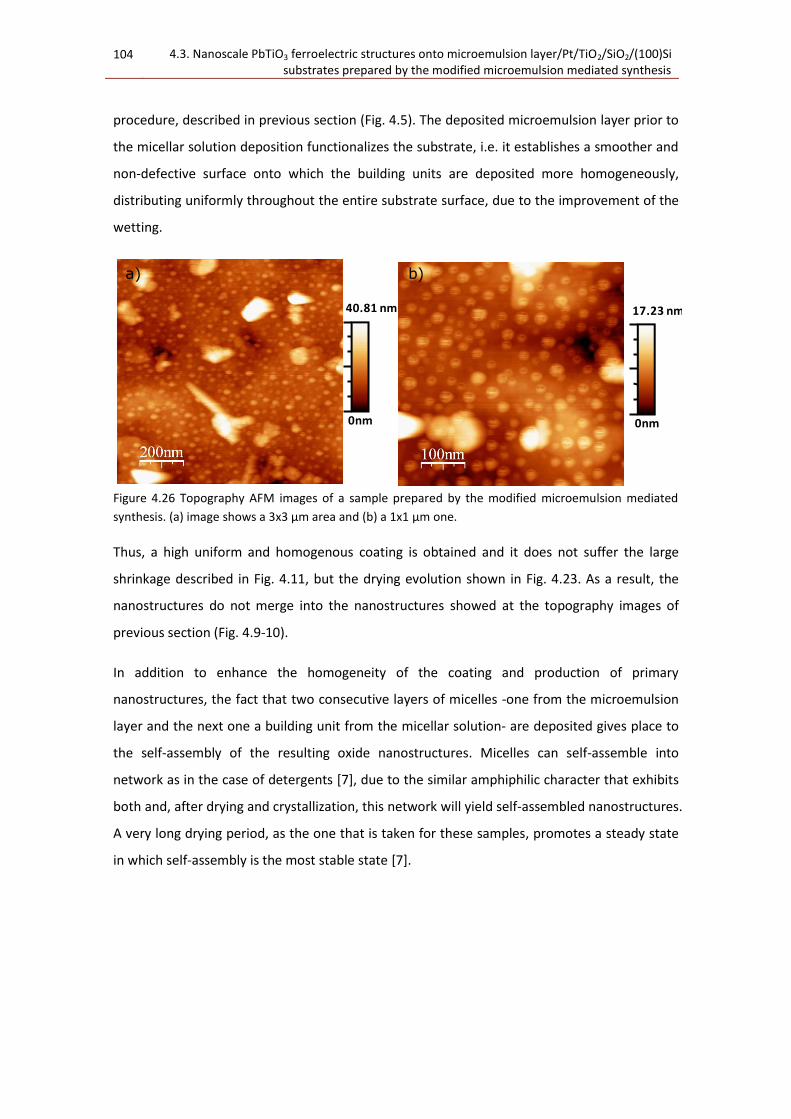
104 4.3. Nanoscale PbTiO3 ferroelectric structures onto microemulsion layer/Pt/TiO2/SiO2/(100)Si substrates prepared by the modified microemulsion mediated synthesis
procedure, described in previous section (Fig. 4.5). The deposited microemulsion layer prior to
the micellar solution deposition functionalizes the substrate, i.e. it establishes a smoother and
non-defective surface onto which the building units are deposited more homogeneously,
distributing uniformly throughout the entire substrate surface, due to the improvement of the
wetting.
Figure 4.26 Topography AFM images of a sample prepared by the modified microemulsion mediated
synthesis. (a) image shows a 3x3 µm area and (b) a 1x1 µm one.
Thus, a high uniform and homogenous coating is obtained and it does not suffer the large
shrinkage described in Fig. 4.11, but the drying evolution shown in Fig. 4.23. As a result, the
nanostructures do not merge into the nanostructures showed at the topography images of
previous section (Fig. 4.9-10).
In addition to enhance the homogeneity of the coating and production of primary
nanostructures, the fact that two consecutive layers of micelles -one from the microemulsion
layer and the next one a building unit from the micellar solution- are deposited gives place to
the self-assembly of the resulting oxide nanostructures. Micelles can self-assemble into
network as in the case of detergents [7], due to the similar amphiphilic character that exhibits
both and, after drying and crystallization, this network will yield self-assembled nanostructures.
A very long drying period, as the one that is taken for these samples, promotes a steady state
in which self-assembly is the most stable state [7].
17.23 nm
0nm
40.81 nm
0nm
a) b)

Chapter 4: Ferroelectric nanostructures by microemulsion mediated synthesis onto Pt/TiO2/SiO2/(100)Si substrates.
105
Figure 4.27. AFM topography images of two different locations in the substrate and their corresponding
self-correlations, (a) and (b).
Fig. 4.27 shows self correlation images of portions of two different AFM topography images, in
which bigger nanostructures are not observed. It demonstrates the periodic order self-
assembly of the primary nanostructures up to the third neighbours. In the case of 2-D
structures, there are five possible Bravais lattices: square, hexagonal, rectangular, rectangular
centred, and oblique [40], as the ones presented in Fig. 4.28.
Figure 4.28. The five fundamental 2-dimensional Bravais lattices[40].
16nm
24
nma) b) c) c)
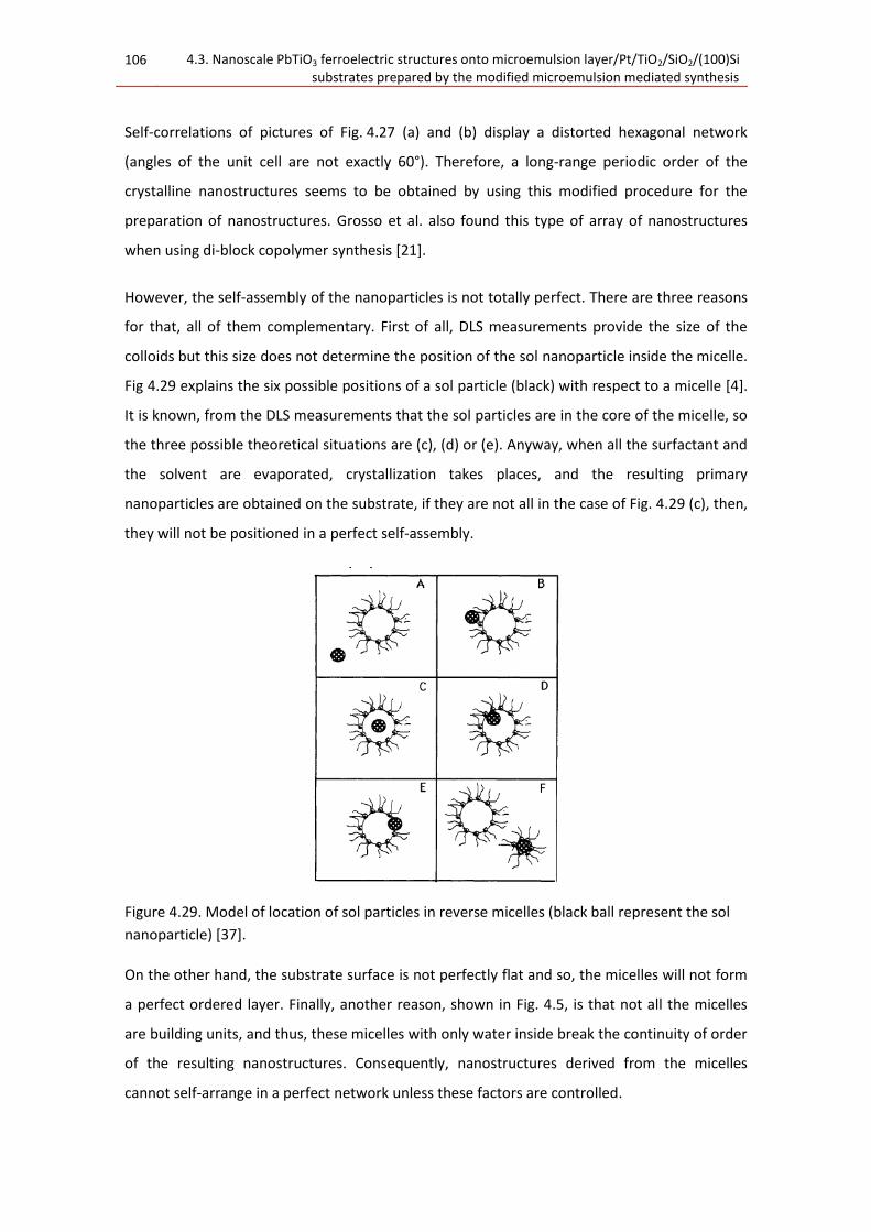
106 4.3. Nanoscale PbTiO3 ferroelectric structures onto microemulsion layer/Pt/TiO2/SiO2/(100)Si substrates prepared by the modified microemulsion mediated synthesis
Self-correlations of pictures of Fig. 4.27 (a) and (b) display a distorted hexagonal network
(angles of the unit cell are not exactly 60°). Therefore, a long-range periodic order of the
crystalline nanostructures seems to be obtained by using this modified procedure for the
preparation of nanostructures. Grosso et al. also found this type of array of nanostructures
when using di-block copolymer synthesis [21].
However, the self-assembly of the nanoparticles is not totally perfect. There are three reasons
for that, all of them complementary. First of all, DLS measurements provide the size of the
colloids but this size does not determine the position of the sol nanoparticle inside the micelle.
Fig 4.29 explains the six possible positions of a sol particle (black) with respect to a micelle [4].
It is known, from the DLS measurements that the sol particles are in the core of the micelle, so
the three possible theoretical situations are (c), (d) or (e). Anyway, when all the surfactant and
the solvent are evaporated, crystallization takes places, and the resulting primary
nanoparticles are obtained on the substrate, if they are not all in the case of Fig. 4.29 (c), then,
they will not be positioned in a perfect self-assembly.
Figure 4.29. Model of location of sol particles in reverse micelles (black ball represent the sol
nanoparticle) [37].
On the other hand, the substrate surface is not perfectly flat and so, the micelles will not form
a perfect ordered layer. Finally, another reason, shown in Fig. 4.5, is that not all the micelles
are building units, and thus, these micelles with only water inside break the continuity of order
of the resulting nanostructures. Consequently, nanostructures derived from the micelles
cannot self-arrange in a perfect network unless these factors are controlled.

Chapter 4: Ferroelectric nanostructures by microemulsion mediated synthesis onto Pt/TiO2/SiO2/(100)Si substrates.
107
The size distributions of the nanostructures shown in the SEM (Fig. 4.25 (a)) and AFM
topography images (Fig. 4.26) are represented in Fig. 4.30. The size distribution of the
nanostructures presented in Fig. 4.30 (a) is bimodal and the one corresponding to the primary
nanoparticles at the AFM topography image is Gaussian (Fig. 4.30 (b)).
The fitting of their probabilistic lines is analitically expressed by:
y = -2.29 + 0.03·x R = 0.99 (4.3)
y = -2.24 + 0.02·x R = 0.99 (4.4)
for the nanostructures shown at the SEM image Fig. 4.20 (a)
y = -5.76 + 0.25·x R = 0.99 (4.5)
for those displayed at the AFM topography image Fig. 4.23 (a).
Figure 4.30. Equivalent diameter distributions of the nanostructures measured on the SEM image of Fig.
4.25 (a) and the AFM image of Fig. 4.26 (a). Straight lines in the cumulative frequency graph represent
the fitting of the probabilistic lines. There are two in the case of the bimodal distribution (red and blue
lines of (a)).
Following this procedure, the average equivalent diameter calculated for the nanostructures of
the SEM image are 65 nm and 92 nm with a standard deviation of 28 nm and 41 nm,
0.01
0.5
2
10
30
50
70
90
98
99.5
0 100 200
0 100 200
0
25
50
75
Co
un
ts
Deq (nm)
Cu
mu
lative
Fre
qu
en
cy
a)
0,01
0,5
2
10
30
50
70
90
98
99,5
12 14 16 18 20 22 24 26 28 30 32
12 14 16 18 20 22 24 26 28 30 32
0
10
20
30
40
Co
un
ts
Deq(nm)
Cu
mu
lative
Fre
qu
en
cy
b)

108 4.3. Nanoscale PbTiO3 ferroelectric structures onto microemulsion layer/Pt/TiO2/SiO2/(100)Si substrates prepared by the modified microemulsion mediated synthesis
respectively. As for the AFM images, the equivalent diameter calculated for the primary
nanostructures is 21 nm with a standard deviation of 4 nm.
Both the bimodal and the single distributions are Gaussian, supporting the hypothesis
established in the previous section: nanostructures obtained by this method are formed by the
merging of primary ones, instead of the most common process in ceramics and thin films in
which coalescence and growth from different nucleus of growth takes place and gives rise to
lognormal distribution of particle size.
The nanostructures prepared by the microemulsion mediated synthesis in previous section 4.2
from a micellar solution of sol concentration 5·10-3 M present an average equivalent diameter
of 67 nm (section 4.2.1). This value is comparable with one of the average sizes calculated for
the bimodal distribution, confirming the hypothesis of nanostructures prepared by the first
procedure as resulting from coalescence of primary ones.
By the modified procedure presented in this section, primary nanostructures are, mainly,
prevented from merging into larger ones and those are the ones corresponding to the single
distribution of average size 21 nm. However, there are still a number of primary nanoparticles
that merge into bigger ones, and those are the ones that have a bimodal distribution and a size
comparable with the ones in section 4.2. In that section, the calculated distribution is a
Gaussian and it is not bi-modal, probably because there is not enough statistics to see it.
TEM measurements were carried out in order to investigate the structure of the
nanostructures as well as the substrate/nanostructure interface.
Fig. 4.31 shows bright-field TEM images of cross sections of three nanostructures: two of them,
of ~162 and ~175 nm of lateral size and a smaller one of ~25 nm. Their profiles present
rounded irregular top facets of ~25 nm of width. This support the hypothesis established in
section 4.2.1 of large nanostructures formed by merging of primary ones. In Fig. 4.31 (d), the
primary nanostructures that might yield the observed ~175 nm nanostructure (Fig. 4.31 (c)),
are highlighted in blue. The size of these hypothetical primary nanostructures is smaller than
25 nm of lateral size. AFM topography images provided an average lateral size of ~21 nm,
which is in agreement with the hypothetical size of the primary nanostructures. From these
images it is clear that primary nanostructures set one aside the next one and not on top of it.

Chapter 4: Ferroelectric nanostructures by microemulsion mediated synthesis onto Pt/TiO2/SiO2/(100)Si substrates.
109
Figure 4.31 Bright-field TEM images of cross section of an isolated nanostructure (a), three
nanostructures formed by the coalescence of primary ones (a-c) and simulated primary nanostructures
disposition (d) that yield the nanostructure in picture above it.
Fig. 4.32 shows the cross-section image of an isolated nanostructure of ~9 nm of lateral size
and ~7 nm of height. (100) planes are easily observed, parallel to the surface of the substrate.

110 4.3. Nanoscale PbTiO3 ferroelectric structures onto microemulsion layer/Pt/TiO2/SiO2/(100)Si substrates prepared by the modified microemulsion mediated synthesis
The edge of the nanostructure is rounded, almost hemispherical. Isolated small nanostructures
(primary ones) are spherical as confirmed by these TEM images. A sphere is the minimum
energy configuration as so, it is logical that the isolated nanostructures and the corrugation of
the merged big nanostructures are spheres. One can argue that, since the micelles are
spherical and spherical nanopowders have been fabricated from them, it is consistent to find
semi-spherical nanostructures on top the substrate. However, after the drying step, a thermal
treatment is performed. The energy supplied to the system is enough to change the
morphology of the nanostructures if necessary for minimum energy reasons.
Figure 4.32. Bright field TEM image of the cross section of an isolated primary nanostructure
Fig. 4.33 (a-b) shows different higher magnification images of the nanostructures, where the
(101) planes are easily distinguishable. In Fig. 4.33 (a), they all have the same orientation with
respect to the substrate surface. Fig. 4.33 (b) shows two different regions where (100) planes
can be observed with a relative rotation of 17.5° (the edge of each region is marked by the last
planes, in blue). The merging region or tilt boundary presents a number of edge dislocations of
spacing D = 1.63 nm and Burger vector |b| = 4.9 Å, calculated using the relation |b| = D·sin θ.
This kind of boundary is usually called “pure tilt boundary” and it was suggested [41] that low-
angle boundaries between adjoining crystallites or crystal grains consist of arrays of
dislocations, as in this case.

Chapter 4: Ferroelectric nanostructures by microemulsion mediated synthesis onto Pt/TiO2/SiO2/(100)Si substrates.
111
Fig. 4.33 (c) shows the (001) planes of a PbTiO3 nanostructure. In this image, the edge
dislocations inside of the nanostructures are highlighted. This result, combined with the one
obtained in Fig. 4.32 indicates that the orientation of the nanostructure is (001). The sample is
crystallized in the cubic phase (650 :C) and during the cooling step and subsequent phase
transition is when the unit cells lengthen in one direction and set the orientation as (100) or
(001). This is the minimum energy type of growth [42].
Figure 4.33 High magnification bright-field HRTEM images of the inside of the nanostructures (a) (101)
planes, (b) (101) planes in adjoining parts of the nanostructure with a relative tilt of 17.5 ° and (c) edge
dislocation, marked with an arrow.

112 4.3. Nanoscale PbTiO3 ferroelectric structures onto microemulsion layer/Pt/TiO2/SiO2/(100)Si substrates prepared by the modified microemulsion mediated synthesis
Defects as vacancies or impurities might clamp their movement, clamping the ferroelectric
domains and yielding piezoresponse hysteresis loops with the shape of the one presented in
Fig. 4.18 (c).
In all the images presented in the above TEM study, it is clear that the substrate
/nanostructure interface is clean and that some nanostructures contain dislocations. Residuals
coming from the preparation procedure used (i.e. a layer with residuals of the precursor
microemulsion, amorphous phases, …) are not observed.
The (101) planes, shown in Fig. 4.33 (a-b), correspond to the same nanostructure. The distance
between them is ~2.9 Å of average. Fig. 4.33 (c) presents the (001) planes with an interplanar
distance of 4.0 Å of average. The planes (100) of Fig. 4.32 are ~3.7 Å of average. This indicates
a tetragonal unit cell and thus a perovskite phase with lattice parameters smaller than the
theoretical ones. However, these measurements are local ones and it is difficult to extrapolate
these results without further statistics.
To conclude, these measurements confirm the perovskite phase and the small size of the
primary nanostructures. They also confirm the formation of larger nanostructures by the
merging of primary ones.
4.3.2. Structural characterization
Fig. 4.34 displays the 2-dimensional synchrotron X-ray diffraction pattern of the sample
prepared from the 5·10-3 M micellar solution.
The pattern consists of four broad peaks and four sharp rings. The maximum intensity is found
at the broad peaks and at certain positions of the rings sectors.
Fig. 4.35 shows the integration of the experimental 2-D diffraction pattern, in solid black and
the simulated lead titanate and platinum diffraction peaks in red and blue, respectively. Each
peak corresponds to one of the sharp rings or broad ring portions of the 2-D diffraction pattern.
It presents four peaks. The most intense peaks correspond to the polycrystalline platinum of
the substrate, having also contributions of PbTiO3 perovskite phase.

Chapter 4: Ferroelectric nanostructures by microemulsion mediated synthesis onto Pt/TiO2/SiO2/(100)Si substrates.
113
Fi
gure
4.3
4. E
xper
imen
tal 2
-D s
ynch
rotr
on
x-r
ay d
iffr
acti
on
pat
tern
of
a sa
mp
le p
rep
ared
fro
m t
he
5·1
0-3
M m
icel
lar
solu
tio
n.

114 4.3. Nanoscale PbTiO3 ferroelectric structures onto microemulsion layer/Pt/TiO2/SiO2/(100)Si substrates prepared by the modified microemulsion mediated synthesis
Figu
re 4
. 35
2θ
dif
frac
tio
n p
atte
rn c
alcu
late
d f
rom
th
e in
tegr
atiio
n o
f th
e 2
-D e
xper
imen
tal p
atte
rn o
f Fi
g. 4
.34
(b
lack
so
lid li
ne)
an
d s
imu
late
d d
iffr
acti
on
pat
tern
s o
f th
e P
bTi
O3
per
ovs
kite
nan
ost
ruct
ure
s (r
ed
lin
e) a
nd
Pt
bo
tto
m e
lect
rod
e (b
lue
line)
.
Intensity(a.u.)
2θ

Chapter 4: Ferroelectric nanostructures by microemulsion mediated synthesis onto Pt/TiO2/SiO2/(100)Si substrates.
115
Figu
re
4.3
6.
Exp
erim
enta
l 2
-D
dif
frac
tio
n
pat
tern
w
ith
re
fle
ctio
ns
corr
esp
on
din
g to
P
t (a
) an
d
Pb
TiO
3 p
ero
vski
te
(b)
and
th
e si
mu
late
d
2-D
d
iffr
acti
on
p
atte
rn
of
po
lycr
ysta
llin
e p
lati
nu
m w
ith
(1
11
) fi
ber
tex
ture
(c)
an
d P
bTi
O3
nan
ost
ruct
ure
s w
ith
(1
00
) fi
ber
tex
ture
.
(111)
(111)
(200)
(200)
(111)
(111)
(200)
(200)
(010)
(111)
(110)
(100)
(110)
(100)
a)
b)
c)
d)
(010)
(111)
(110)
(100)
(110)
(100)

116 4.3. Nanoscale PbTiO3 ferroelectric structures onto microemulsion layer/Pt/TiO2/SiO2/(100)Si substrates prepared by the modified microemulsion mediated synthesis
Fig. 4.36 shows a more detailed identification of the broad spots and ring sectors of the 2-D
diffraction pattern. Simulation of the diffraction peaks for the polycrystalline platinum layer
explains the broad diffraction peaks as resulting of a (111) fiber texture with an orientation
distribution cone of ±3°, as was previously observed for the ultrathin film in section 3.2.2. The
simulated pattern was calculated from the inverse pole figure. Fig. 4.36 (c) shows this
simulation.
Fig. 4.36 (d) shows the simulated diffraction pattern for the PbTiO3 perovskite phase,
considering the lattice parameters to be a = b = 3.890(0) Å and c = 4.056(7) Å. It is the result of
adding up the simulated diffraction patterns for all the crystals with axis rotated (-7:, -7:, ±20:)
and (20:, -7:, -7:±20:) as seen in the TEM image of Fig. 4.32 (b), where (101) planes presented
a tilt angle of 17.5°. The crystalline distortion is c/a = 1.042(8), much smaller than the
theoretical one (1.066(8) being, a = 3.899(9) Å and c = 4.150(0) Å). The results for the ultrathin
film in previous section 3.2.2 imply lattice parameters equal to a = b = 3.912(1) Å and
c = 4.130(1) Å.
A previous study [43] indicates that, after the drying step in a sol-gel deposition procedure, a
thin film is subjected to tensile stresses, which explains the lattice distortion of the ultrathin
film. However, it is reported in the same work as well as others [44, 45] that this stress is
minimized with film thickness. Primary nanostructures fabricated by this procedure are ~10
nm of height and the uncoated substrate surface is much larger than the area occupied by the
oxide nanostructures. In addition, drying time is very long, so this source of stress should be
minimized and cannot explain by itself the smaller distortion of the nanostructures.
Previous works in nanopowders fabricated by a microemulsion mediated synthesis proved the
high crystallinity of the ones prepared by this procedure [18, 22], which means that variation in
the crystallinity throughout the sample is not contemplated as a reason for a low tetragonal
distortion. The size of the nanostructures here presented is one of the smallest for individual
structures onto substrates reported in the literature. Due to the so small size of the
nanostructures, the crystal lattice is subjected to stress, yielding the distortion in the c
direction that explains such a small tetragonal distortion.
The 2-D diffraction pattern of an ultrathin film (section 3.2.2), also shows a crystalline
distortion smaller than the theoretical one that was attributed to stresses due to the mismatch
between the substrate and the PbTiO3 perovskite phase and the different thermal expansion

Chapter 4: Ferroelectric nanostructures by microemulsion mediated synthesis onto Pt/TiO2/SiO2/(100)Si substrates.
117
of the platinum layer and the PbTiO3 ultrathin film. Both reasons apply here and most probably
are6 the main cause for the stress found.
The primary nanostructures observed by bright-field HRTEM presented an interplanar distance
of ~2.85 Å for the (101) planes of one merged nanostructure and ~3.71 Å for the (100) planes
of a primary nanostructure. These distances imply different values of the lattice parameters of
these individual nanostructures. However, the values obtained by X-ray diffraction represent
an average value of all the nanostructures present at the sample.
It was not possible to simulate the diffraction pattern from the inverse pole figure. The sample
does not have a well defined fiber texture and it is not possible to apply the statistical
describer the Anaelu software uses [46]. Not being a continuous sample, it might be that there
is not a polycrystalline structure with a valid statistic. Thus, we have to speak about crystals or
small groups of crystals. This reinforces the hypothesis of these particles as primary ones.
4.3.3. Functional characterization
PFM measurements were performed on the isolated nanostructures prepared by this modified
microemulsion mediated synthesis, using a 5·10-3 M. Images corresponding to the out-of-plane
polarization are shown in Fig. 4.37.
The experiments were carried out at the Max Plank Institute for Microstructure Physics under
an AC field of amplitude 1.5V -peak to peak- and at a frequency close to the contact resonance
of the cantilever (245kHz) in order to enhance the measurements using the ATEC-EFM
cantilevers, as explained in Chapter 2 (Experimental Procedure, Section 2.6).
The image shows nanostructures with different phase and amplitude. 180: phase difference
can be observed at Fig. 4.37 (d) and through the amplitude profile (Fig. 4. 37 (e)).
The out-of–field hysteresis loop of an isolated nanostructure, shown in Fig, 4.38, verifies the
ferro-piezoelectric character of these PbTiO3 nanoparticles. It is asymmetric with respect to
the piezoresponse and the voltage axis. As discussed in section 3.2.3, it means that the
nanostructure has a certain imprint [47] and a certain offset due to the presence of a pinned
layer [48]. In a previous Section, Fig. 4.33 (b) showed two regions of the same nanostructure
with a relative tilt of the (101) planes and edge dislocations that enable such tilt. This is a
probable area where charges can clamp the motions of the dislocations creating a pinned area
that would be too small to switch.

118 4.3. Nanoscale PbTiO3 ferroelectric structures onto microemulsion layer/Pt/TiO2/SiO2/(100)Si substrates prepared by the modified microemulsion mediated synthesis
Figu
re 4
.37
. To
po
grap
hy
(a),
ph
ase
(b)
and
am
plit
ud
e (c
) o
ut-
of-
pla
ne
pie
zore
spo
nse
im
ages
fo
r th
e is
ola
ted
nan
ost
ruct
ure
s o
f a
sam
ple
pre
par
ed b
y th
e
mo
dif
ied
mic
roem
uls
ion
syn
thes
is m
eth
od
. Im
age
(d)
corr
esp
on
ds
to a
hig
h m
agn
ific
atio
n im
age
; it
s p
has
e p
rofi
le (
e) a
re m
arke
d in
blu
e in
th
e p
has
e im
age.
20
0nm
20
0n
m2
00
nm
PZ
27
.80
nm
0n
m
11
pm
/V
0.0
0
PFM
Im
age
Am
plit
ude im
age
PFM
Im
age
Phase im
age
AFM
Im
age
Out-
of-
pla
ne
a)
b)
c)
150
100
50
0
12
10 8 6 4 2 0
X[n
m]
Z[µm]
+90º
-90º0º
d)
e)

Chapter 4: Ferroelectric nanostructures by microemulsion mediated synthesis onto Pt/TiO2/SiO2/(100)Si substrates.
119
This hysteresis loop shows both kinds of asymmetries from the very first loop. As in the case of
the merged nanostructures from previous section, there is a certain initial polarization, which
means that there are charges on the surface of the substrate prior to the application of any DC
field. The fact that regardless the sample and the procedure followed to obtain the isolated
nanostructures the same initial polarization is obtained, might mean that microemulsion
mediated synthesis, combined with a CSD method as the one here used, yield to
nanostructures with a defined initial polarization that gives rise to the surface charges and not
the other way around. Previous studies on ferroelectric perovskite materials grown epitaxial
onto single crystal substrates suggested that the elastic accommodation of the in-plane strain
could lead to an enhancement of the spontaneous polarization of simple ferroelectric
perovskites along the out-of-plane direction [49].
Measurement conditions: Vac = 1.5V
Freq ac = 235kHz F = 30 nN
Tbias = 0.2s Tmeasurement = 0.3s
SEN = 2mV TC = 0.1 s
Figure 4.38. Piezoresponse hysteresis loop obtained in the nanostructure, which phase profile is shown
in Fig. 4.37 (e). Its lateral size is ~37 nm and its height is ~15 nm as measured from the images of
Fig. 4.37.
The effect of the pinned layer is more important in this case than it was for the nanostructures
prepared by the instability of ultrathin films in previous Chapter 3 (section 3.2) and the
nanostructures prepared by the non modified procedure of previous section 4.2. It was
explained before that this effect occurs at the interface between the substrate and the
nanostructure and that the smaller the nanostructure is, the more relevant this effect
becomes. Consequently, the hysteresis loop is shifted so much that, most of it, is in the
positive side of the piezoresponse axis.
-10 -8 -6 -4 -2 0 2 4 6 8 10
-10
0
10
20
30
40
50
Pie
zo
resp
on
se
(a
.u.)
Voltage (V)

120 4.3. Nanoscale PbTiO3 ferroelectric structures onto microemulsion layer/Pt/TiO2/SiO2/(100)Si substrates prepared by the modified microemulsion mediated synthesis
In this case, an increase of the piezoresponse near the coercive voltage is not observed, as it
was for the merged nanostructures. This might indicate that the non-pinned layer is a single
domain that switches 180°. Ferroelectric PbTiO3 nanodots were found to present a stable
polarization due to surface charges, instead of the supposed vortex state [50]. This state could
only be reverted by 180° switching, as it is happening in the nanostructures prepared by this
modified method.
The smallest size where ferroelectricity has been demostrated by PFM has been in
nanostructures of 41 nm of lateral size [51, 52], while the nanostructure which hysteresis loop
is here represented is ~37 nm, becoming one of the smallest nanostructures where ferro-
piezoresponse is proved by PFM to date. Note that the resolution of SPM in contact mode is
compromised when the dimension of the measured nanostructures is equal or smaller than
the one of the tip [53]. Actually, the real dimensions of the nanostructure are even smaller, as
shown previously by TEM, where primary nanostructures with ~8.99 are observed.

Chapter 4: Ferroelectric nanostructures by microemulsion mediated synthesis onto Pt/TiO2/SiO2/(100)Si substrates.
121
Remarks
1. At the micellar solution, micelles act as building units, isolating the sol nanoparticles
inside the core of the micelle and yielding, after drying and thermal treatment of the
coatings, the nanostructures onto the Pt/TiO2/SiO2/(100)Si substrates.
2. By using a combination of microemulsion mediated synthesis and CSD, nanostructures
with controlled size and shape are obtained. Size does not depend on the sol
concentration: the average size of the crystalline nanostructures obtained by this
procedure is ~75 nm for the ones prepared from the 10-2 M micellar solution and
~67 nm for those prepared from the 5·10-3 M one. Only the number of nanostructures
on the substrate does. Those nanostructures are not ordered.
3. Nanostructures prepared by this procedure are formed by merging of primary ones.
Size distributions are Gaussian, i.e. the formation of the nanostructures does not take
place via normal grain growth, but from a limited number of primary nanostructures.
This is due to the capillary forces during drying that attract micelles to each other, as
well as to the defects of the substrate surface and bad wetting of the coating.
4. PFM images show ferro-piezoresponse of the nanostructures, proving their
ferroelectric character. Mechanism of switching in these nanostructures is complex,
involving 90° switching of a domains and the creation of a pinned layer, stabilized by
the charges on the surface of the platinum bottom electrode of the substrate that
introduce themselves at the domain wall.
5. This first procedure does not provide a periodic array of ordered nanostructures onto
the substrate. In order to improve the wetting and to minimize the shrinkage of the
micellar solution coating during drying, a modification of the previous preparation
method is proposed, in which a microemulsion layer will constitute the surface onto
which the micellar solution will be spun-coated. In this way, isolated primary
nanostructures with size distributions of average size ~21 nm are obtained as observed
on the AFM images, as well as a reduced number of merged bigger ones.
6. TEM results proved that isolated nanostructures down to ~9 nm of lateral size can be
observed. These nanostructures are found all over the sample, showing the uniformity
and quality of the coating. Both the primary nanostructures and larger, merged ones
show Gaussians size distributions.

122 Remarks
7. The primary nanostructures prepared by this late modified procedure shows
hexagonal order. A long-range order is not observed due to the presence of some
merged bigger nanoparticles, the inhomogeneous surface of the platinum substrate ,
the fact that not all the deposited micelles are building units and, probably, to the fact
that not all sol nanoparticles are exactly at the center of the building units.
8. The synchrotron radiation x-ray diffraction pattern of the nanostructures obtained by
the modified method shows PbTiO3 perovskite reflections with cell parameters
a=b=3.890(0) Å and c=4.056(7) Å and crystal axis rotated (-7°, -7°, ±20°) and (20°, -7°, -
7°±20°). The reason for this tetragonal distortion smaller than the theoretical one
might be the stress due to the large surface area to volume ratio of the sample that
implies the small size of the nanostructures, the mismatch between substrate and
nanostructure lattices and the different thermal expansion coefficients of both of
them.
9. Nanostructures obtained by this modified procedure are ferroelectric and seem to be
single domains over a pinned layer. Ferro-piezoresponse is measured in this work in
one of the smallest nanostructures where this kind of measurements could be carried
out by PFM to date, with lateral size of ~37 nm as determined by AFM topography
images.
Bibliography. 123
Bibliography
[1] H. Wennerstrom and B. Lindman, "Micelles - physical-chemistry of surfactant
association", Physics Reports-Review Section of Physics Letters, 52 (1), 1979, p:1
[2] W.D. Harkins, "A general theory of the reaction loci in emulsion polymerization II", The
journal of chemical physics, 13, 1945, p:47
[3] K. Landfester, "The generation of nanoparticles in miniemulsions", Advanced materials,
13 (10), 2001, p:765
[4] M.P. Pileni, "Reverse micelles as microreactors", Journal of Physical Chemistry, 97,
1993, p:6961
[5] C. Tanford, "The hydrophobic effect and the organization of living matter", Science,
200, 1978, p:1012
[6] S. Mann, S.L. Burkett, S.A. Davis, C.E. Fowler, N.H. Mendelson, S.D. Sims, D. Walsh and
N.T. Whilton, "Sol-gel synthesis of organized matter", Chemistry of Materials, 9 (11), 1997,
p:2300
[7] C.J. Brinker, Y.F. Lu, A. Sellinger and H.Y. Fan, "Evaporation-induced self-assembly:
Nanostructures made easy", Advanced materials, 11 (7), 1999, p:579
[8] D. Grosso, F. Cagnol, G. Soler-Illia, E.L. Crepaldi, H. Amenitsch, A. Brunet-Bruneau, A.
Bourgeois and C. Sanchez, "Fundamentals of mesostructuring through evaporation-induced
self-assembly", Advanced Functional Materials, 14 (4), 2004, p:309
[9] G. Schinkel, I. Garrn, B. Frank, U. Gernert, H. Schubert and R. Schomacker, "Fabrication
of alumina ceramics from powders made by sol-gel type hydrolysis in microemulsions",
Materials Chemistry and Physics, 111 (2-3), 2008, p:570
[10] J. Tartaj and P. Tartaj, "Two-Stage Sintering of Nanosize Pure Zirconia", Journal of the
American Ceramic Society, 92 (1), 2009, p:S103
[11] D.E. Zhang, Z.W. Tong, S.Z. Li, X.B. Zhang and A.L. Ying, "Fabrication and
characterization of hollow Fe3O4 nanospheres in a microemulsion", Materials letters, 62 (24),
2008, p:4053
[12] M. Boutonnet, J. Kizling, P. Stenius and G. Maire, "The preparation of monodisperse
colloidal metal particles from microemulsions", Colloids and Surfaces, 5 (3), 1982, p:209
[13] S. Hingorani, V. Pillai, P. Kumar, M.S. Multani and D.O. Shah, "Microemulsion mediated
synthesis of zinc-oxide nanoparticles for varistor studies", Materials Research Bulletin, 28 (12),
1993, p:1303
[14] Y.F. Lu, H.Y. Fan, A. Stump, T.L. Ward, T. Rieker and C.J. Brinker, "Aerosol-assisted self-
assembly of mesostructured spherical nanoparticles", Nature, 398 (6724), 1999, p:223
124 Bibliography
[15] K.P. Das and J.E. Kinsella, "Stability of food emulsions: physicochemical role of protein
and nonprotein emulsifiers", Advances in Food and Nutrition Research, 34, 1990, p:81
[16] Y.L. Khmelnitsky, A.V. Levashov, N.L. Klyachko and K. Martinek, "Engineering
biocatalytic systems in organic media with low water-content", Enzyme and Microbial
Technology, 10 (12), 1988, p:710
[17] T.H. McHugh, "Protein-lipid interactions in edible films and coatings", Nahrung-Food,
44 (3), 2000, p:148
[18] C. Beck, W. Härtl and R. Hempelmann, "Size-controlled synthesis of nanocrystalline
BaTiO3 by a sol-gel type hydrolysis in microemulsion-provided nanoreactors", Journal of
Materials Research, 13 (11), 1998, p:3174
[19] S. Bhattacharyya, S. Chattopadhyay and M. Alexe. "Fabrication of isolated ferroelectric
nanostructures". in Materials Research Society Symposium. 2003. San Francisco.
[20] S. Clemens, S. Rohrig, A. Rudiger, T. Schneller and R. Waser, "Embedded ferroelectric
nanostructure arrays", Nanotechnology, 20 (7), 2009, p:5
[21] D. Grosso, C. Boissiere, B. Smarsly, T. Brezesinski, N. Pinna, P.A. Albouy, H. Amenitsch,
M. Antonietti and C. Sanchez, "Periodically ordered nanoscale islands and mesoporous films
composed of nanocrystalline multimetallic oxides", Nature Materials, 3 (11), 2004, p:787
[22] H. Herrig and R. Hempelmann, "A colloidal approach to nanometre-sized mixed oxide
ceramic powders", Materials letters, 27, 1996, p:287
[23] S. Kronholz, S. Rathgeber, S. Karthauser, H. Kohlstedt, S. Clemens and T. Schneller,
"Self-assembly of diblock-copolymer micelles for template-based preparation of PbTiO3
nanograins", Advanced Functional Materials, 16 (18), 2006, p:2346
[24] L.S. Ee, J. Wang, S.C. Ng and L.M. Gan, "Low temperature synthesis of PZT powders via
microemulsion processing", Materials Research Bulletin, 33 (7), 1998, p:1045
[25] C. Pithan, Y. Shiratori, R. Waser, J. Dornseiffer and F.H. Haegel, "Preparation,
processing, and characterization of nano-crystalline BaTiO3 powders and ceramics derived
from microemulsion-mediated synthesis", Journal of the American Ceramic Society, 89, 2006,
p:2908
[26] H. Herrig and R. Hempelmann, "Microemulsion mediated synthesis of ternary and
quaternary nanoscale mixed oxide ceramic powders", Nanostructured Materials, 9 (1-8), 1997,
p:241
[27] C. Pithan, Y. Shiratori, A. Magrez, S.B. Mi, J. Dornseiffer and R. Waser, "Consolidation,
microstructure and crystallography of dense NaNbO3 ceramics with ultra-fine grain size",
Journal of the Ceramic Society of Japan, 114 (1335), 2006, p:995

Bibliography. 125
[28] Y. Yamashita, H. Yamamoto and Y. Sakabe, "Dielectric properties of BaTiO3 thin films
derived from clear emulsion of well-dispersed nanosized BaTiO3 particles", Japanese Journal of
Applied Physics, 43 (9B), 2004, p:6521
[29] J. Kim, J.K. Kim, S. Heo and H.S. Lee, "Ferroelectric properties of sol-gel prepared La-
and Nd-substituted, and Nb-co-substituted bismuth titanate using polymeric additives", Thin
Solid Films, 503 (1-2), 2006, p:60
[30] S.S. Kim, E.K. Choi, J.K. Kim, J.S. Kim, T.K. Song and J. Kim, "Effects of surfactant on
surface morphology and orientation of Nb-doped Bi4Ti3O12 thin films", Journal of the Korean
Physical Society, 42, 2003, p:S1126
[31] M.P. Pileni, "The role of soft colloidal templates in controlling the size and shape of
inorganic nanocrystals", Nature Materials, 2, 2003, p:145
[32] J. Tyndall, "On the Blue Colour of the Sky, the Polarization of Skylight, and on the
Polarization of Light by Cloudy Matter Generally", Proceedings of the Royal Society of London,
17, 1868, p:223
[33] M. Ramirez, J. Bullon, J. Anderez, I. Mira and J.L. Salager, "Drop size distribution
bimodality and its effect on O/W emulsion viscosity", Journal of Dispersion Science and
Technology, 23 (1-3), 2002, p:309
[34] C.J. Brinker and G.W. Scherer, Sol-gel science. The physics and chemistry of sol-gel
processing. 1990, San Diego: Academic Press.
[35] C. Beck, W. Härtl and R. Hempelmann, "Size-controlled synthesis of nanocrystalline
BaTiO3 by a sol-gel type hydrolysis in microemulsion-provided nanoreactors", Journal of
Materials Research, 13 (11), 1998, p:3174-3180
[36] H. Herrig and R. Hempelmann, "A colloidal approach to nanometre-sized mixed oxide
ceramic powders", Materials letters, 27, 1996, p:287-292
[37] M.P. Pileni, "Reverse micelles as microreactors", Journal of Physical Chemistry, 97,
1993, p:6961-6973
[38] M.P. Pileni, "The role of soft colloidal templates in controlling the size and shape of
inorganic nanocrystals", Nature Materials, 2, 2003, p:145-150
[39] G. Decher, Layered nanoarchitectures via directed assembly of anionic and cationic
molecules. Comprenhesice supramolecular chemistry, ed. J.-P. Sauvage and M.W. Hosseini. Vol.
9. 1996, Oxford: Pergamon Press.
[40] C. Hammond, Introduction to crystallography. Royal Microscopical Society. Microscopy
Handdbooks. Vol. 19. 1992, Oxford: Oxford university press.
[41] C. Kittel, Introduction to solid state physics. 6th ed. 1986, New York: Wiley.

126 Bibliography
[42] J. Ricote, R. Poyato, M. Algueró, L. Pardo and L. Calzada, "Texture development in
modified lead titanate thin films obtained by chemical solution deposition on silicon-based
substrates", Journal of the American Ceramic Society, 86 (9), 2003, p:1571
[43] J. Mendiola, M.L. Calzada, P. Ramos, M.J. Martin and F. Agulló-Rueda, "On the effects
of stresses in ferroelectric (Pb, Ca)TiO3 thin films", Thin Solid Films, 315, 1998, p:195
[44] A. Bartasyte, O. Chaix-Pluchery, J. Kreisel, C. Jimenez, F. Weiss, A. Abrutis, Z. Saltyte
and M. Boudard, "Investigation of thickness-dependent stress in PbTiO3 thin films", Journal of
Applied Physics, 103 (1), 2008, p:014103
[45] T. Ohno, B. Malic, H. Fukazawa, N. Wakiya, H. Suzuki, T. Matsuda and M. Kosec. "Origin
of compressive residual stress in alkoxide derived PbTiO3 thin film on Si wafer". in 25th
Meeting on Ferroelectric Materials and Their Applications (FMA-25). 2008. Kyoto, JAPAN.
[46] L. Fuentes, "Anomalous scattering and null-domain ghost corrections for fibre
textures", Textures and Microstructures, 10, 1989, p:347
[47] H.N. AlShareef, D. Dimos, W.L. Warren and B.A. Tuttle, "Voltage offsets and imprint
mechanism in SrBi2Ta2O9 thin films", Journal of Applied Physics, 80 (8), 1996, p:4573
[48] B.J. Rodriguez, S. Jesse, M. Alexe and S.V. Kalinin, "Spatially Resolved Mapping of
Polarization Switching Behavior in Nanoscale Ferroelectrics", Advanced materials, 20 (15),
2008, p:102
[49] M.-W. Chu, I. Szafraniak, R. Scholz, C. Harnagea, D. Hesse, M. Alexe and U. Gösele,
"Impact of misfit dislocations on the polarization instability of epitaxial nanostructured
ferroelectric perovskites", Nature Materials, 3, 2004, p:87
[50] J. Wang and M. Kamlah, "Domain control in ferroelectric nanodots through surface
charges", Applied Physics Letters, 93 (26), 2008, p:262904
[51] A. Roelofs, I. Schneller, K. Szot and R. Waser, "Piezoresponse force microscopy of lead-
titanate nanograins possibly reaching the limit of ferroelectricity", Applied Physics Letters, 81
(27), 2002, p:5231
[52] A. Roelofs, T. Schneller, K. Szot and R. Waser. "Towards the limit of ferroelectric
nanosized grains". in 3rd International Conference on Trends in Nanotechnology. 2002.
Santiago Composte, Spain: Iop Publishing Ltd.
[53] J.S. Villarrubia, "Algorithms for scanned probe microscope image simulation, surface
reconstruction, and tip estimation", Journal of Research of the National Institute of Standards
and Technology, 102 (4), 1997, p:425

CHAPER 5: NANOSTRUCTURES ONTO SrTiO3 SINGLE-
CRYSTAL SUBSTRATES BY MICROEMULSION MEDIATED
SYNTHESIS
5.1. Towards ideal surfaces
Previously, in Chapter 4, it was shown that the deposition of micellar solutions onto Pt coated
Si based substrates yield PbTiO3 ferroelectric nanostructures and that the self-arrangement of
primary nanostructures can be achieved on polycrystalline substrates. However, such
nanostructures presented a number of defects related to the lattice mismatch between the
polycrystalline Pt top layer and the PbTiO3 grown nanostructures that were observed either
directly (see Fig. 4.28 where dislocations are found inside the bulk nanostructures) or indirectly
from the piezoelectric measurements at local scale (see Fig. 4.17, Fig. 4.35 and the discussion
that follows).
It was proposed as a target of this thesis to learn about effects derived from the scaling down
of the size of the nanostructures. But it is difficult to separate these effects from the extrinsic
ones due to the mismatch between the substrate and the PbTiO3 nanostructures [1]. By using
a single crystal substrate, as will be done in this Chapter, surface, nanostructure crystal
structure and nanostructures defects should be minimized and this can lead to better
ferroelectric performance while keeping the nano-scale size and ordering of the
nanostructures.
The selected single crystal is SrTiO3 (STO) often used to promote epitaxial growth of
ferroelectric perovskites by a number of techniques (sputtering, PLD, etc…) [1-6]. At room
temperature, STO has a cubic cell (space symmetry 𝑃 4 𝑚 3 2 𝑚 , space group 221) with
lattice parameters a = 3.900(5) Å and a perovskite like structure. This structure can be
described as stacks of alternating layers of SrO and TiO2 planes.
In previous Chapter 4, micelles were proved as valid building units to obtain isolated
nanostructures onto Pt coated Si(100) substrates. Thus, the combination of a single crystal
substrate with lattice parameters close to the ones of the PbTiO3 perovskite, and the
microemulsion mediated synthesis previously discussed, is supposed to yield primary
nanostructures with a periodic order and that would grow epitaxially on the substrate surface.

128 5.2. Nanoscale PbTiO3 structures onto commercial as-served SrTiO3 substrates prepared by
microemulsion mediated synthesis
5.2. Nanoscale PbTiO3 structures onto commercial as-served SrTiO3
substrates prepared by microemulsion mediated synthesis.
Quality of the substrate surfaces is important. This surface should be as close as possible to an
ideal one to preserve, over macroscopic surface areas, the expected arrangement of the
micelles in the solution-derived layer and in the resulting crystalline nanostructures after heat
treatment. In this study, one side polished commercial (100)SrTiO3 substrates will be used as
served.
Fig. 5.1 shows the AFM topography images of an as-received STO substrate. Terraces of the
substrate vary in length and width and they present a non-well defined edges.
Figure 5.1 AFM topography images of an as-served SrTiO3 substrate (a-b) and profile (d) along the blue
line of image (c).
The surface of the substrate was analyzed by LEED and AES. It was not possible to measure the
as-received substrates due to the strong charging effects and the, as expected, contaminated
surface. Even if they were used after a surface cleaning treatment, contact with the
5004003002001000
7
6
5
4
3
2
1
0
X[nm]
Z[Å
]a) b)
19.33 Å
0.00 Å
c) d)

Chapter 5: Nanostructures onto SrTiO3 single-crystal substrates by microemulsion mediated synthesis
129
atmosphere would contaminate them and turn them to the previous state. It is a well known
fact that SrO reacts with CO2 and H2O at room temperature to form carbonate and hydroxide
compounds following the reaction:
3SrO + 2CO2 + H2O → Sr(OH)2 + 2SrCO3 (5.1)
and, therefore, contaminating the substrate surface.
Micellar solutions with concentrations of 10-2 M and 5·10-3 M were deposited onto the as-
served STO substrates and thermally treated by RTP at 650°C (as explained in Chapter 2,
section 2.3) to obtained the crystalline PbTiO3 nanostructures that are studied next.
5.2.1. Microscopy analysis.
When using the microemulsion mediated synthesis combined with CSD technology onto a
commercial as-served SrTiO3 substrate, coating of the substrate is not uniform. Fluid steam
rings, as shown in Fig. 5.2, are formed during deposition, drying and thermal treatment of
crystallization, mainly due to a non-uniform wetting of the substrate by the micellar solution
and, consequently, non homogenous evaporation of the solvent during the spin-coating and
drying steps.
Figure 5.2. Optical image of the surface of a sample prepared onto a commercial and as-received SrTiO3
substrate.
A detailed study using SEM was performed along one of the radii of the quasi-circular coating,
revealing the different morphology of the coating depending on the distance to the thickest
area (Fig. 5.3). Thus, the coating formed by the inner rings, which are closer, presents an
50 µm

130 5.2. Nanoscale PbTiO3 structures onto commercial as-served SrTiO3 substrates prepared by
microemulsion mediated synthesis
Figu
re 5
.3.
SEM
im
ages
of
the
mo
rph
olo
gy o
f th
e sa
mp
le p
rep
ared
fro
m t
he
5·1
0-3
M m
icel
lar
solu
tio
n o
nto
an
as-
rece
ived
STO
su
bst
rate
in
dep
end
ence
of
the
thic
knes
s o
f th
e co
atin
g al
on
g th
e su
bst
rate
su
rfac
e.
d=
120
0μm
d=
640
0μm
d=
320
0
μm
III
IIIIV
V
IIIV
V
IIII
-bIII
-a
[100
][0
10
][1
00]
[01
0]
[100
][0
10]
[100
][0
10
][1
00]
[010
]
Ce
nte
r o
f th
eco
ati
ng
Bo
rder
of
the
coat
ing
[10
0]
[010
]

Chapter 5: Nanostructures onto SrTiO3 single-crystal substrates by microemulsion mediated synthesis
131
almost continuous deposit, where some pyramids of rounded facets protrude (area I in Fig.
5.3). At outer rings, a network of lines of similar width can be observed (area II in Fig. 5.3),
following the [100] and [010] directions of the substrate. When the amount of deposited
material decreases at outer rings, the continuous network breaks into truncated pyramids of
square and rectangular basis that may merge (Fig. 5.3, area III) following the same directions
than the initial network of lines. For even outer rings, there is so little material that the
incipient truncated pyramids coexist with round small PbTiO3 nanostructures (area IV, Fig. 5.3).
Despite the non uniform coating, in some areas, a 2-dimensional short range periodicity of the
nanostructures is found. These arrays follow the *100+ direction and a 45⁰ direction, most
probably the [110] one. Directions are established with respect to the facets of the single
crystal. A similar morphology is found, despite of the concentration of the micellar solution
used.
The estimated size of the square based pyramids of area III-b (Fig. 5.3) is ~50 nm while the
rectangular based ones are ~20-50 nm wide and ~100 nm long. The isolated nanostructures
formed in area V are ~30 nm of lateral size.
The fact that areas with different thickness and topography are found when using
microemulsions have been already reported by Carvalho et al. [7]. They prepared block
copolymers films and observed a similar phenomenon to the one here described that depends
on the relative thickness of the coating of the different areas, as seen in Fig. 5.4.
Figure 5.4. SEM image of the morphology of a coating of a block-copolymer film [7].
However, the morphology of the different areas depends on the type of growth of the
nanostructures onto the substrate. When the phase formation phenomena do not depend on

132 5.2. Nanoscale PbTiO3 structures onto commercial as-served SrTiO3 substrates prepared by
microemulsion mediated synthesis
the kinetics of nucleation and growth, the mode of nucleation on foreign substrate may be
formulated on the basis of macroscopic thermodynamic considerations [8], taking into account
the surface and interface energies for lattice mismatch systems [9]. Results shown in previous
Chapter 4 already proved that this is the case when using the microemulsion mediated
synthesis, as the nanostructures prepared by this method present Gaussian size distributions,
which are related to independent nucleation points, either isolated building units or groups of
these (see sections 4.2.1 and 4.3.1).
Growth can be categorized in three different modes, summarized in Fig. 5.5.
a) the Frank-van der Merwe mode , when the adhesion between the substrate and the
growing structure is strong and the relative mismatch is small. It is a layer by layer type
of growth and before growing a new layer, the old one should be complete.
b) the Stranski-Krastanov mode, in the case of strong adhesion between the growing
structure and the substrate and a relatively large mismatch. After the completion of a
certain number of monolayers, 3-dimensional cluster of structures grow onto them.
c) the Volmer-Webber mode, for a weak adhesion between substrate and growing
structure. 3-dimensional cluster are observed right from the beginning. The relative
mismatch between the crystalline lattices determines the strain to which the 3-
dimension nuclei are subjected.
If the SEM images are considered as a scheme of how the isolated nanostructures and
subsequent continuous films grow onto the substrate (supposing the growing steps in this
order: Fig 5.3 (V), (IV), (III-a), (III-b), (II), (I)), it can be concluded that they follow the Frank-van
der Merwe growing mode, as it would be expected for the small lattice mismatch between
SrTiO3 and PbTiO3 and the strong adhesion when the last layer of the substrate or the first one
from the nanostructure is the shared TiO2 one.
AFM topography images of Fig. 5.6 confirm the results obtained from the SEM images and
provide additional information about the arrangement of the nanostructures onto the
substrate surface. Topography images of this figure can be related to those of Fig. 5.3. From
the profile of the topography images, it can be estimated that the nanostructures grow onto
the cotinuous thin film (zone I) with a lateral size of ~ 25-30 nm, the square pyramids of
zone III have a ~ 100 nm base and the rectangular ones a 50x250 nm2 base. Nanostructures of
zone V in Fig. 5.6 seem not to be isolated as it was expected from the SEM images. As it was

Chapter 5: Nanostructures onto SrTiO3 single-crystal substrates by microemulsion mediated synthesis
133
Figu
re 5
.5.
Sch
emat
ic t
heo
reti
cal
cro
ss-s
ecti
on
vie
ws
of
the
thre
e m
od
es
of
thin
film
gro
wth
. Ea
ch m
od
e is
sh
ow
n f
or
con
secu
tive
per
iod
s o
f ti
me
and
su
bse
qu
ent
surf
ace
cove
rage
[8
, 9].
t=t 1
sub
stra
tesu
bst
rate
sub
stra
te
t=t 2
>t 1
sub
stra
tesu
bst
rate
sub
stra
te
t=t 3
>t 2
>t 1
sub
stra
tesu
bst
rate
sub
stra
te
a) F
ran
k-va
n d
er
Me
rwe
mo
de
b) S
tran
ski-
Kra
stan
ov
mo
de
c) V
olm
er-
We
bb
er m
od
e

134 5.2. Nanoscale PbTiO3 structures onto commercial as-served SrTiO3 substrates prepared by
microemulsion mediated synthesis
already explained in section 2.4.5, lateral resolution in tapping mode is compromised when the
measured structures have the same size or are smaller than the probe. Therefore, in this case,
these nanostructures are observed as non-isolated nanostructures of ~37 nm of lateral size,
even if SEM images provided more accurate data.
A lower magnification image of the same of zone III of Fig. 5.6 is displayed in Fig. 5.7. Long
truncated rectangular based pyramids (Fig. 5.7(c)) coexist with squared based ones (Fig. 5.7
(b)). The first ones are in the micron range (~1 µm long, ~150 nm wide), while the last ones can
be classified as nanostructures of lateral size of ~150 nm. Their height is similar, despite the
shape or the orientation as can be confirmed by the color scale. These nanostructures onto the
substrate follow the [100] and [010] directions, setting at the surface minimum energy areas,
that is to say, the terraces edges.
These results indicate an important role of the surface of the substrate on the shape and
positioning of the nanostructures depending on the configuration of the terraces of the SrTiO3
substrate surface.
As seen in Fig. 5.6, nanostructures grown onto these substrates try to be placed in the
minimum energy locations of the substrate surface. Thus, they try to follow the terraces of the
substrate. By annealing the samples at high temperatures (850°C and 1050°C), it was observed
how the nanostructures settle at the terraces, as very small isolated particles at the edge (Fig.
5.8 (b) and (d)) or as pyramids with facets parallels to the terraces and placed at their corners
(Fig. 5.8 (a),(c) and (e)), depending on the amount of material (and subsequent relative
thickness) of the initial coating. The morphology of the surface of the substrate plays a major
role in the arrangement of the nanostructures. However, re-crystallization at high temperature
modifies the morphology of the nanostructures, as it provides additional energy and promotes
merging of the already present nanostructures

Chapter 5: Nanostructures onto SrTiO3 single-crystal substrates by microemulsion mediated synthesis
135
Figu
re 5
.6.
AFM
to
po
grap
hy
imag
es
of
thre
e d
iffe
ren
t zo
nes
of
the
sam
ple
pre
par
ed f
rom
th
e 5
·10
-3 M
mic
ella
r so
luti
on
. Th
e p
rofi
les
dis
pla
yed
bel
ow
eac
h i
mag
e
corr
esp
on
d t
o t
he
blu
e lin
es d
epic
ted
in t
he
AFM
imag
es
abo
ve t
hem
.
III
IIIIV
V
17
.43
nm
0.0
0 n
m
25
02
00
15
01
00
50
0
5 4 3 2 1 0
X[n
m]
Z[nm]
Com
plet
edth
infi
lm
Nan
ostr
uctu
res
27
.49
nm
0.0
0 n
m
Squa
repy
ram
id
Rec
tang
ular
pyr
amid
11
.13
nm
0.0
0 n
m
200nm
Na
no
stru
ctu
res
VIII
I

136 5.2. Nanoscale PbTiO3 structures onto commercial as-served SrTiO3 substrates prepared by
microemulsion mediated synthesis
Figu
re 5
.7.
Low
mag
nif
icat
ion
AFM
to
po
grap
hy
imag
e o
f zo
ne
III-
b o
f Fi
g. 5
.3 (
a) a
nd
tw
o r
epre
sen
tati
ve z
oo
m a
reas
wh
ere
sq
uar
e tr
un
cate
d p
yram
ids
(b)
and
rect
angu
lar
on
es (
c) c
an b
e fo
un
d a
nd
th
eir
pro
file
s al
on
g th
e b
lue
lines
mar
ked
in t
he
AFM
imag
es.
44
.45
nm
0.0
0 n
m
1.6
1.4
1.2
10
.80
.60
.40
.20
25
20
15
10 5 0
X[µ
m]
Z[nm]
17
.62
nm
0.0
0 n
m
25
02
00
15
01
00
50
0
16
14
12
10 8 6 4 2 0
X[n
m]
Z[nm]
71
.19
nm
0.0
0 n
m
tran
sver
sal
lon
gitu
din
al
b)
c)
a)

Chapter 5: Nanostructures onto SrTiO3 single-crystal substrates by microemulsion mediated synthesis
137
Figu
re 5
.8.
Sam
ple
s p
rep
ared
fro
m t
he
10
-2 M
mic
ella
r so
luti
on
at
65
0°C
an
d r
e-c
ryst
alliz
ed a
t 8
50
°C (
a-b
) an
d 1
05
0°C
(c-
e).
Imag
e (b
) sh
ow
s a
hig
her
mag
nif
icat
ion
imag
e o
f (a
). Im
ages
(d
) an
d (
e) a
re h
igh
er m
agn
ific
atio
n im
ages
of
(c)
and
are
pre
sen
ted
her
e to
sh
ow
det
ails
of
the
mer
ged
nan
ost
ruct
ure
s an
d t
he
mo
dif
icat
ion
of
the
sub
stra
te w
ith
tem
per
atu
re.
5.9
8 n
m
-4.9
9 n
m
3.6
3 n
m
-3.0
8 n
m
a)b
)
26
.54
nm
-6.8
5 n
m
5.6
5 n
m
-3.0
1 n
m
200nm
42
.06
nm
-6.5
0 n
m
c)d)
e)

138 5.2. Nanoscale PbTiO3 structures onto commercial as-served SrTiO3 substrates prepared by
microemulsion mediated synthesis
5.2.2. Structural characterization
Fig. 5.9 shows the experimental 2-dimensional synchrotron X-ray diffraction pattern of one the
samples prepared in this section.
The pattern consists of sharp short arcs and some diffuse spots. The most representative spots
are zoomed as inset in Fig. 5.9.
Integration of this experimental 2-D diffraction pattern is displayed in Fig. 5.10 as a black line.
The simulated PbTiO3 and SrTiO3 crystal perovskite phases are also presented in red and blue,
respectively. The most intense peaks correspond to the (100) SrTiO3 single crystal substrate,
having also contributions of the PbTiO3 perovskite phase.
Fig. 5.11 presents the simulated patterns of the SrTiO3 substrate and the PbTiO3
nanostructures in their perovskite structure. Note that not all the simulated peaks of the
PbTiO3 are present at the real pattern due to the low relative intensities of such peaks. A
certain cone of directions of angular width of ±3⁰ had been used for the simulations. The
lattice parameters calculated for the PbTiO3 from the simulations were a = b = 3.896(6)Å and
c = 4.149(4) Å, almost the theoretical ones (a = b = 3.899(9)Å and c = 4.140(0) Å).
The experimental Debye sharp ring sections agree well with the diffraction maxima of SrTiO3.
Measured SrTiO3 ring sections correspond to crystal orientation characterized by (001) poles
approximately normal to the sample surface. The diffuse spots of Fig. 5.9 always appear on the
low angle side of the SrTiO3 sharp peaks. This indicates a crystal phase with larger lattice
parameters than SrTiO3. These maxima fit to PbTiO3 perovskite reflections. The orientation
similarity and close cell parameters of the substrate and the PbTiO3 phase indicate that the
PbTiO3 nanostructures have grown epitaxially onto the SrTiO3 substrate. This epitaxial growth
explain partially why the lattice parameters are closer to the theoretical ones than the ones
obtained onto Pt/TiO2/SiO2/(100)Si substrates.
Besides, from the semiquantitative analysis of the broadening of the peaks assigned to PbTiO3,
it is deduced that these structures have nanometric sizes, as previously observed from the
topographic image of Fig. 5.3 (zone V), and that they are under strained conditions, which also
agrees with results reported for Pb(Zr0.42Ti0.48)O3 perovskite structures onto SrTiO3 substrates
[10, 11].

Chapter 5: Nanostructures onto SrTiO3 single-crystal substrates by microemulsion mediated synthesis
139
Figu
re 5
.9. E
xper
imen
tal 2
-D s
ynch
rotr
on
x-r
ay d
iffr
acti
on
pat
tern
of
a sa
mp
le p
rep
ared
fro
m t
he
5·1
0-3
M m
icel
lar
solu
tio
n o
nto
as-
rece
ived
STO
su
bst
ate.

140 5.2. Nanoscale PbTiO3 structures onto commercial as-served SrTiO3 substrates prepared by
microemulsion mediated synthesis
Figu
re 5
.10
. 2θ
dif
frac
tio
n p
atte
rn c
alcu
late
d f
rom
th
e in
tegr
atio
n o
f th
e 2
-D e
xper
imen
tal p
atte
rn o
f Fi
g. 5
.9 (
bla
ck s
olid
lin
e) a
nd
sim
ula
ted
dif
frac
tio
n p
atte
rns
of
the
Pb
TiO
3 p
ero
vski
te n
ano
stru
ctu
res
(red
lin
e) a
nd
SrT
iO3
sub
stra
te(b
lue
on
e).
2θ
Intensity(counts)

Chapter 5: Nanostructures onto SrTiO3 single-crystal substrates by microemulsion mediated synthesis
141
Figu
re 5
.11
. Si
mu
late
d 2
-D d
iffr
acti
on
pat
tern
of
sin
gle
crys
tal S
rTiO
3 w
ith
(0
01
) fi
ber
te
xtu
re (
a) a
nd
Pb
TiO
3 n
ano
stru
ctu
res
wit
h (
00
1)
text
ure
(b
) .
The
exp
erim
enta
l 2-D
dif
frac
tio
n p
atte
rns
wit
h r
efle
ctio
ns
corr
esp
on
din
g to
th
e Sr
TiO
3 an
d t
he
Pb
TiO
3 p
ero
vski
te p
has
es a
re s
ho
wn
in (
c) a
nd
(d
), r
esp
ect
ivel
y.
a)b
)
c)d
)
(11
0)
(11
0)
(11
1)
(20
0)
(21
1)
(21
1)
(22
0)
(22
0)
(11
0)
(11
1) (2
00
)
(21
1)
(21
1)
(22
0)
(22
0)
(11
0)
(11
0)
(11
0)
(11
1)
(20
0)
(21
1)
(21
1)
(22
0)
(22
0)
(11
0)
(11
1) (2
00
)
(21
1)
(21
1)
(22
0)
(22
0)
(11
0)
(20
0)
(00
1)
(10
1)
(11
0)
(20
0)(1
11
)
(11
2)
(21
1)(2
02
)
(22
0)
(10
1) (1
10
)(2
00
)
(11
1)
(11
2)
(21
1)
(20
2)
(22
0)
(20
0)
(20
0)
(00
1)
(10
1)
(11
0)
(20
0)(1
11
)
(11
2)
(21
1)(2
02
)
(22
0)
(10
1) (1
10
)(2
00
)
(11
1)
(11
2)
(21
1)
(20
2)
(22
0)
(20
0)

142 5.2. Nanoscale PbTiO3 structures onto commercial as-served SrTiO3 substrates prepared by
microemulsion mediated synthesis
Therefore, these analyses show that the nanostructures prepared by the microemulsion aided
sol–gel method onto as-received STO (100) substrates have a PbTiO3 perovskite structure with
a (100) preferred orientation.
5.2.3. Functional characterization
In order to prove the ferroelectric character of these nanostructures, measurements were
carried out on them by PFM. For this, new samples were deposited onto as-received
conductive Nb-doped (100)SrTiO3 substrates from the 5·10-3 M micellar solution.
Local piezoelectric and phase hysteresis loops were measured in the regions of the coating
where the self-arranged isolated nanostructures are observed (see zone V, Fig. 5.3). Also, the
piezoelectric activity of the larger particles with pyramid morphology was evaluated.
Fig. 5.12 shows the out-of-field piezoresponse hysteresis loops for an AC voltage at the free
resonance of the cantilever corresponding to the isolated nanostructures -(a) and (b)- and the
truncated pyramids -(c) and (d)-.
Figure 5.12. Out-of-field local hysteresis loops of isolated nanostructures of ~40 nm of lateral size
(phase (a) and amplitude (b) loops) and truncated squared based pyramid of ~400 nm of lateral size
(phase (c) and amplitude (d) loops).
In both cases, the hysteresis loops are symmetric with respect to the voltage axis and show a
high bias. This high bias is related to a certain imprint of the nanostructure [12], a well known
b)
d)c)
a)
d3
3ef
f(a
.u.)
d3
3ef
f(a
.u.)
Voltage (V) Voltage (V)
Voltage (V) Voltage (V)
Phas
e(⁰
)P
ha
se(⁰
)

Chapter 5: Nanostructures onto SrTiO3 single-crystal substrates by microemulsion mediated synthesis
143
effect in thin films [13] that was also observed in this thesis, in the case of nanostructures
prepared by using the microstructural instability phenomenon (Fig. 3.14) and not on those
prepared by the microemulsion mediated synthesis (Fig. 4.18 and Fig. 4.38).
Both pairs of hysteresis loops are symmetric with respect to the voltage axis, in contrast to the
experiments in section 4.2.3 and 4.3.3 where nanostructures prepared onto
Pt/TiO2/SiO2/(100)Si substrates were non symmetric (Fig. 4.38) or become non symmetric after
the first loop (Fig. 4.18 (c)). These effects were attributed to a pinned volume that is unable to
switch but has a certain polarization. The nature of this volume remains unknown, but is most
probably related to the defects –dislocations- observed in the TEM cross-section images of
section 4.2.1, which movement is clamped by free charges from the surface that are injected
towards the nanostructure. Here, this phenomenon is not observed, indicating that either
there is no defect in the bulk nanostructure or the free charges do not penetrate inside the
nanostructure and, consequently, they do not clamp a domain.
However, measurements on samples prepared onto Nb-doped STO substrates present
problems because, after the thermal treatment of crystallization of the nanostructures, the
substrate becomes less conductor. This destroys the capacitor formed by the bottom
substrate, the PbTiO3 nanostructure and the conductive probe, making difficult the
measurement of the piezoelectric hysteresis loops, most probably due to the migration of the
Nb atoms that increases the resistivity of the substrate. Therefore, it is difficult to extract
useful information from the functional characterization here shown and to compare these
results with the ones from previous chapters, onto Pt-coated (100)Si substrates.
5.3. Nanoscale PbTiO3 structures onto (100)SrTiO3 substrates
with controlled surfaces prepared by microemulsion mediated
synthesis.
As it was observed in previous section 5.2.1, the surface of the substrate plays a key role in the
growth of the nanostructures: it influences the type of growth, the adhesion to the substrate,
the epitaxy and the arrangement of the nanostructures. Therefore, a change in the physico-
chemical properties of the substrate surface will result in a different coating of the substrate
by the solution and, consequently, in a different shape and arrangement of the nanostructures.
This was exploited, for instance, in the work by Gilber et al. [14], who reported the possibility
of preparing, by CSD, self-organized heteroepitaxial CeO2 nanodots by controlling the surface
of LaAlO3 single crystal substrate.

144 5.3. Nanoscale PbTiO3 structures onto SrTiO3 substrates with controlled surfaces prepared by
microemulsion mediated synthesis
Concerning the role of the substrate surface in the PbTiO3/SrTiO3(100) system, Fig. 5.6 showed
that nanostructures preferentially grow at the edges of the STO terraces. Also, Fig. 5.8
illustrated the modification of the surface morphology when the substrate was annealed at
high temperatures. Therefore, it seems that the morphology of the substrate surface actually
influences the arrangement of the deposited nanostructures. However, this is not the only
factor to take into account to grow ferroelectric PbTiO3 nanostructures. In addition, in order to
improve the epitaxy between the SrTiO3(100) single crystal surface and the PbTiO3
nanostructures, the substrate should be finished in TiO2, which is the common layer between
both perovskite structures. In this way, epitaxial growth between nanostructures and
substrate would be enhanced, a less defective structure achieved (because of a uniquely
defined interface) and, consequently, adhesion improved.
As it was said before, the SrTiO3 perovskite structure consists of alternating layers of non-polar
SrO and TiO2, so that the terminating layer of a (100) crystal is not uniquely defined. Since the
SrO and TiO2 terminations present very different surface energies, SrO being more stable than
TiO2 for a wider range of chemical potentials (see Fig. 5.13), one would expect to find a
preferential SrO termination on nominally ideal STO surfaces (e.g., in absence of atmospheric
contaminants). In real surfaces, however, the ratio of the SrO and TiO2 terminated areas is
found to generally depend on surface preparation conditions.
Figure 5.13. Surface energy for TiO2 and SrO termination as a function of the TiO2 chemical potential
(the bulk reference is set to rutile and the zero chemical potential corresponds to the TiO2 rich
condition) [15].
Chapter 5: Nanostructures onto SrTiO3 single-crystal substrates by microemulsion mediated synthesis
145
An additional key point is the fact that re-crystallization at high temperatures (850 °C, 1050°C)
changes the morphology of the nanostructures and does not lead to nanostructures of
controlled shape and size, and uniformly distributed onto the substrate. Controlling such
characteristics is a subject of major importance, since the most probable application of these
ferroelectric nanostructures was pointed out to be their use as NV-FeRAM, Therefore, in the
next sections the surfaces of as-received (100) SrTiO3 substrates will be modified by different
treatments, studying the effect of these modifications on nanostructure growth and
positioning.
5.3.1 Preparing ideal surfaces: chemical and thermal treatments of the
STO surfaces.
The ideal STO (100) surface for heteroepitaxy purposes should be clean, smooth, well terraced
and have a unique type of terminating layer. Different treatments have been previously
reported in the literature for improving the surfaces of SrTiO3 substrates and achieve such
features.
Initially, Kawasaki et al. [16] proposed a mechanism of preparation of atomically smooth
surfaces of STO terminated by a TiO2 layer. Their procedure consists on selectively dissolving
the SrO surface planes, using the fact that the nature of both oxides is different: SrO is a basic
oxide while TiO2 is an acidic one. Thus, controlling the pH of the wet etching solution (Buffered
HydroFluoric acid (BHF)) would result into a substrate finished by the desired oxide layer. Their
chemical treatment consisted on soaking the as received polished substrates in the etching
solution (BHF, pH 4.4-4.6, 10 min), followed by a rinse in pure water and ethanol; finally,
substrates were dried in a nitrogen stream. Based on AFM, low energy ion scattering
spectroscopy (ISS) and reflection high energy electron diffraction (RHEED) measurements, the
authors claimed that the surface of these BHF-treated substrates (without any thermal
treatment) exhibited atomically flat terraces with o.4 nm high steps, and that the terminating
layer was TiO2 with a coverage factor of 100%.
Koster et al. [17] proposed to soak the substrates in a more basic BHF solution (pH= 5.5) and
for less time (30 s), preceding this treatment with a ultrasonically soaking of the as-received
substrate in water, in order to selectively promote the hydroxylation of the topmost SrO layer,
to make it more soluble in the acidic solution used for the etching of the substrate surface. It is
a well known fact that SrO reacts with CO2 and H2O from the atmosphere at room temperature
to form stable Sr compounds (like Sr(OH)2 and SrCO3). At the same time, TiO2 is unlikely to
react with water, due to its high stability. Koster et al. proposed to ultrasonically soak the as-
146 5.3. Nanoscale PbTiO3 structures onto SrTiO3 substrates with controlled surfaces prepared by
microemulsion mediated synthesis
received substrate in water in order to enhance the formation of Sr(OH)2 and thus, the etch-
selectivity of SrO relative to TiO2. To remove possible remnants and facilitate the
recrystallization of step ledges, a final thermal treatment (in a tube oven with flowing O2 ) was
carried out at 950 °C for 1 h, raising the temperature at a rate of about 0.5 °C/s, and cooling
down slowly (in 3 h) to room temperature. Based on AFM, LFM , RHEED and X-ray
photoelectron spectroscopy (XPS) measurements, these authors [17] claim that their
preparation method improves surface morphology (by reducing deep etch pits) and the
reproducibility of the results (by reducing the critical dependence on etching time and pH),
leading to atomically flat -and relatively clean- surfaces with straight terrace ledges and a
nearly perfect single (TiO2) termination.
Others authors [18-22] proposed slights variations of the above procedures and revealed that
a more complex scenario actually accompanies the preparation of such ideal STO surfaces.
Some of these works emphasized the convenience of adding thermal treatments to the
chemical etching proposed in ref. [15], in order to get better results, e.g., to promote ledge
recrystallization and achieve a well terraced morphology with straight steps [18, 21, 22]. To
reduce the pitchs created by the etching, a previous annealing stage it has been suggested [22],
while a repetition of the etching and heating stages it has been proposed to elliminate (or at
least reduce) the Sr-species that are observed to segregate to the surface during post-etching
thermal treatments [18]. Several works [18, 20] pointed out the importance of using specific
structural and compositional techniques to characterize the resulting surfaces, since only
conventional AFM measurements in air may not be able to detect the presence (on the
surface) of small segregated Sr-compounds or of islands half a unit cell high. Finally, a detailed
study by grazing incidence X-ray diffraction (GIXD) has recently found [20] that substrates
prepared by the procedure reported in ref. [17] (or small variations) have a rather high
TiO2/SrO surface termination ratio, but not a 100% TiO2 termination: results suggested that
about 75% of the surface is terminated by a TiO2 layer and about 25% by a SrO layer.
Inspired by these two recipes [16, 17], different processing strategies were carried out here
trying to achieve appropriate STO surfaces terminated by TiO2 planes; they consisted in a
chemical treatment of the commercial (polished) 10x10x1 mm3 SrTiO3(100) substrates,
followed by a thermal treatment. The processed substrates were then studied by AFM, AES
and LEED techniques to analyze the topography, composition and crystal structure of the
resulting surfaces.

Chapter 5: Nanostructures onto SrTiO3 single-crystal substrates by microemulsion mediated synthesis
147
As far as the chemical treatment is concerned, two kinds of experimental procedures were
performed. In the first one (etching-I), substrates were soaked for 20 seconds in a BHF etching
solution of pH 4.3; i.e., within the range reported [16] as adequate to avoid extensive surface
damage. In the second one (etching-II), substrates were ultrasonically soaked in deionized
water for 10 minutes before soaking them in a BHF etching solution of pH = 5.56 for 30 s. In
both procedures, substrates were rinsed in pure (Milli-Q) water after etching, and dried in a N2
stream.
Thermal treatments were carried out either in ultra high vacuum (UHV) or in air, in both cases
without oxygen gas flow. Details on the respective experimental conditions can be found in
section. Substrates were annealed up to temperatures high enough to allow recrystallization
processes. In particular they were heated above 800 ⁰C, the reported threshold for regrowth
of the step edges [17, 22]. Extremely low cooling rates were selected in all cases, in order to
promote the steady state [17, 23] and avoid the formation of undesired droplet-like features
on the STO surfaces [23].
Figure 2.4 in Chapter 2 schematically describes the two experimental procedures followed in
UHV. In the first one (thermal-A), a slow heating rate of ~0.1 ⁰C /s was used up to reach 815 ±
5 ⁰C on the substrate surface; this temperature was maintained for 3600 s, and the cooling
rate subsequently applied was even lower (0.03 ⁰C/s). In the second case (thermal-B) values
are slightly higher: a heating rate of ~0.2 ⁰C/s was applied until reaching a surface temperature
of 842 ± 7 ⁰C, which was maintained for 7200 s; cooling down to room temperature was also
performed with a very low rate ( ~0.09 ⁰C/s).
In the case of the thermal treatment in air (thermal-C), the STO substrate was annealed much
faster (heating rate of ~30 ⁰C/s) by using a rapid thermal processor (RTP). The annealing
temperature, kept for 3600 s, was also significantly higher (1050 ⁰C). Nevertheless, for cooling
down to room temperature, a very low rate was selected: ~0.1 ⁰C/s.
Table 5.1 summarizes the different STO (100) substrates processed here, together with their
respective treatments. It can be seen that, besides the samples chemically etched, there is
another one (labelled “substrate 1”) simply cleaned by Ar+ ion bombardment (60 min, 3 µA,
0.6-1 kV) and annealing in UHV (thermal-A conditions). This susbtrate was prepared in order to
have a clean surface reference for the Auger signals and LEED patterns, because some of the
procedures here investigated have not been previously analyzed in the literature (or at least
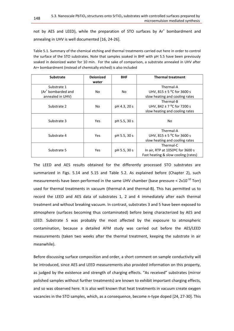
148 5.3. Nanoscale PbTiO3 structures onto SrTiO3 substrates with controlled surfaces prepared by
microemulsion mediated synthesis
not by AES and LEED), while the preparation of STO surfaces by Ar+ bombardment and
annealing in UHV is well documented [16, 24-26].
Table 5.1. Summary of the chemical etching and thermal treatments carried out here in order to control
the surface of the STO substrates. Note that samples soaked in BHF with pH 5.5 have been previously
soaked in deionized water for 10 min. For the sake of comparison, a substrate annealed in UHV after
Ar+ bombardment (instead of chemically etched) is also included
Substrate Deionized water
BHF Thermal treatment
Substrate 1 (Ar
+ bombarded and
annealed in UHV) No No
Thermal-A UHV, 815 ± 5 ⁰C for 3600 s
slow heating and cooling rates
Substrate 2 No pH 4.3, 20 s Thermal-B
UHV, 842 ± 7 ⁰C for 7200 s slow heating and cooling rates
Substrate 3 Yes pH 5.5, 30 s
No
Substrate 4 Yes pH 5.5, 30 s Thermal-A
UHV, 815 ± 5 ⁰C for 3600 s slow heating and cooling rates
Substrate 5 Yes pH 5.5, 30 s Thermal-C
In air, RTP at 1050ºC for 3600 s Fast heating & slow cooling (rates)
The LEED and AES results obtained for the differently processed STO substrates are
summarized in Figs. 5.14 and 5.15 and Table 5.2. As explained before (Chapter 2), such
measurements have been performed in the same UHV chamber (base pressure < 2x10⁻¹⁰ Torr)
used for thermal treatments in vacuum (thermal-A and thermal-B). This has permitted us to
record the LEED and AES data of substrates 1, 2 and 4 immediately after each thermal
treatment and without breaking vacuum. In contrast, substrates 3 and 5 have been exposed to
atmosphere (surfaces becoming thus contaminated) before being characterized by AES and
LEED. Substrate 5 was probably the most affected by the exposure to atmospheric
contamination, because a detailed AFM study was carried out before the AES/LEED
measurements (taken two weeks after the thermal treatment, keeping the substrate in air
meanwhile).
Before discussing surface composition and order, a short comment on sample conductivity will
be introduced, since AES and LEED measurements also provided information on this property,
as judged by the existence and strength of charging effects. “As received” substrates (mirror
polished samples without further treatments) are known to exhibit important charging effects,
and so was observed here. It is also well known that heat treatments in vacuum create oxygen
vacancies in the STO samples, which, as a consequence, become n-type doped [24, 27-30]. This

Chapter 5: Nanostructures onto SrTiO3 single-crystal substrates by microemulsion mediated synthesis
149
doping causes a darkening of the substrates and substantially increases sample conductivity,
thus facilitating surface analysis by STM or electron spectroscopy and diffraction techniques.
Both effects have been observed here for substrates 1, 2 and 4: after UHV heating, sample
colour changed from light yellow to dark grey, and no charging was detected during AES or
LEED measurements. In contrast, substrate 5 (annealed in air) exhibited some charging effects
(less than “as received” substrates) and did not become dark. The most remarkable result was
found on substrate 3: this “as etched” surface (without further thermal treatments) shows a
significant reduction of charging effects, suggesting surface conductivities not only better than
those of “as received” samples, but even better than that of substrate 5, (i.e., better than
samples annealed in air after etching).
Illustrative LEED patterns of all the substrates are presented in Fig. 5.14. Since they have been
recorded for different energies and sample azimuths, in order to facilitate data analysis, the
energy of the incident electron beam is indicated in each case, identifying also a few selected
diffraction spots. Patterns displayed on the left column correspond to substrate 1, while those
on the central and right columns belong to chemically etched substrates; among the later,
those depicted on the top and central raws correspond to substrates annealed at high
temperatures.
The surface of substrate 1 exhibits excellent 1x1- SrTiO3 (100) LEED patterns (Fig. 5.14 (a), (c),
(f)). This surface thus keeps the 1x1 bulk structure without additional reconstructions, in
agreement with previous reports for similar substrate treatments (Ar+ bombardment and
annealing in UHV) [24-26]. Note the low background and very sharp and brilliant spots of these
patterns, which indicate a well defined 2D nature and global ordering (i.e. good crystal quality)
of the surface region, suggesting also surface cleanness.
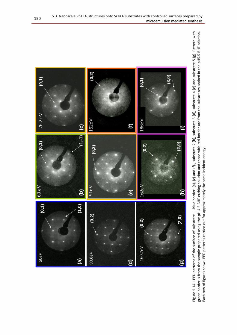
150 5.3. Nanoscale PbTiO3 structures onto SrTiO3 substrates with controlled surfaces prepared by
microemulsion mediated synthesis
Figu
re 5
.14
. LE
ED p
atte
rns
of
the
surf
ace
of
sub
stra
te 1
-b
lue
bo
rder
: (a
), (
c) a
nd
(f)
-, s
ub
stra
te 2
(b
), s
ub
stra
te 3
(d
), s
ub
stra
te 4
(e)
an
d s
ub
stra
te 5
(g)
. P
atte
rn w
ith
gree
n b
ord
er is
fro
m t
he
sam
ple
pre
par
ed u
sin
g th
e p
H 4
.5 B
HF
etch
ing
solu
tio
n a
nd
th
ose
wit
h r
ed b
ord
er a
re f
rom
th
e su
bst
rate
s so
aked
in t
he
pH
5.5
BH
F so
luti
on
.
Each
ro
w o
f fi
gure
s sh
ow
LEE
D p
atte
rns
carr
ied
ou
t fo
r ap
pro
xim
atel
y th
e sa
me
inci
den
t en
ergy
.
60
eV(0
,1)
(1,0
)
(0,1
)7
6.2
eV
60
eV
(0,1
)
(1,-
1)
90
.8eV
16
0.7
eV(0
,2)
(2,0
)
(0,2
)
16
2eV
(0,2
)
(2,0
)
91
eV
(0,2
)
18
6eV
(0,1
)
(3,0
)
152
eV
(0,2
)
(a)
(b)
(c)
(d)
(e)
(f)
(g)
(h)
(i)

Chapter 5: Nanostructures onto SrTiO3 single-crystal substrates by microemulsion mediated synthesis
151
Such cleanness is further confirmed by the Auger spectra of substrate 1 (see black line in Fig.
5.15), at least within the detection limit of the instrument (i.e., AES signals from possible
contaminants, like carbon, if exist, are below 0.1 atomic monolayer). On the other hand, peaks
from the Sr(MMN), Ti(LMM) and O(KLL) Auger transitions are clearly visible (energy regions of
50-130eV, 350-430 eV and 470-520 eV, respectively), with line-shapes and energies
characteristic of STO surfaces [25, 29, 31]. The Sr(104 eV), Ti(382 eV) and O(510 eV) peaks
(marked by arrows in Fig. 5.15) have been selected for the surface composition analysis, their
relative Sr-to-Ti and O-to-Ti intensity ratios being shown in Table 5.2. It should be noted that
the O-to-Ti intensity ratios measured for substrate 1 (Table 5.2) are found to be in agreement
with literature results for similar substrate treatments [25]. Hence, substrate 1 can be
confidently used as a reference surface for the LEED and AES analysis of STO samples.
Figure 5.15. AES spectra of the surface of substrate 1 (black line), substrate 4(blue line) and substrate 5 (red line), showing the Sr(MMN), Ti(LMM) and O(KLL) Auger transitions in the derivative mode. Arrows mark the peaks considered in the intensity ratio analysis of Table 5.2.
Table 5.2 summarizes the relative intensities of the Sr and O peaks with respect to the Ti, as
well as the observed LEED reconstruction (if any) for the as-received substrates and chemically
etched and/or thermally treated.
50 100 150 200 250 300 350 400 450 500
20000
25000
30000
35000
Inte
nsity
Energy (eV)
Sr peaksTi peaks
Oxygen
50 100 150 200 250 300 350 400 450 500
25000
30000
35000
40000
Inte
nsity
Energy (eV)
50 100 150 200 250 300 350 400 450 500
25000
30000
35000
40000
50 100 150 200 250 300 350 400 450 500
30000
35000
40000
50 100 150 200 250 300 350 400 450 500
20000
25000
30000
35000
Inte
nsity
Energy (eV)
Sr peaksTi peaks
Oxygen
50 100 150 200 250 300 350 400 450 500
20000
25000
30000
35000
Inte
nsity
Energy (eV)
Sr peaksTi peaks
Oxygen
Sr
Ti
O
Substrate 1
Substrate 4
Substrate 5

152 5.3. Nanoscale PbTiO3 structures onto SrTiO3 substrates with controlled surfaces prepared by
microemulsion mediated synthesis
Table 5.2. Auger intensity ratios obtained for the Sr(104 eV), Ti(382 eV) and O(510 eV) peaks, as measured on different STO (100) substrates: “as received” and prepared by the procedures detailed in Table 5.1 The respective surface structures observed by LEED are also indicated.
SrTiO3 substrate LEED IO/ITi ISr/ITi
As-received - 2.5 ± 0.5 1.4 ± 0.15
Substrate 1 1x1 2.7 ± 0.25 1.7 ± 0.2
Substrate 2 c(2x2) 4.1 ± 0.4 5.4 ± 0.5
Substrate 3 (1x1) 2.8 ± 0.2 2.9 ± 0.2
Substrate 4 c(2x2) 3.3 ± 0.3 4.4 ± 0.3
Substrate 5 (1x1) 2.2 ± 0.3 1.2 ± 0.3
Similar LEED patterns are observed for substrate 2 (Fig. 5.14 (b)) and substrate 4 (Fig. 5.14 (c),
(e)), which not only indicate good crystal order in the top layers, but also reveal the presence
of a superstructure. These two substrates (chemically etched and annealed in UHV) exhibit
patterns with the 1x1 diffraction spots characteristic of the bulk structure, and additional
(fractional) spots forming what we think is a centered c(2x2) superstructure (also known as
√2x√2-R245⁰). Note that the surface symmetry observed in both substrates is the same,
independently of whether “etch-I” or “etch-II” procedures have been employed. Their
respective Auger spectra show surfaces free of carbon contamination (see e.g., blue line in Fig.
5. 15, corresponding to substrate 4). Hence, the c(2x2) superstructure is probably due to a
surface reconstruction produced by the rearrangement of oxygen vacancies in the top layers.
In fact, several superstructures (twinned (2x1), c(6x2), c(4x2), (2x2), (√5x√5-R26.6⁰), … ) have
been observed by LEED, RHEED, GIXD, STM or TEM techniques on clean STO (100) surfaces
after diverse thermal treatments, being interpreted as related to different arrangements and
densities of the oxygen vacancies in the surface region [20, 21, 26-30, 32-35]. Noticeably, this
is the first time (to our knowledge) that a c(2x2) superstructure is reported for clean SrTiO3
(100) surfaces, but we are not aware either of structural studies of STO (100) surfaces
prepared in the same conditions as substrates 2 and 4 ( i.e., by chemical etching with a BHF
solution followed by high-T annealing in UHV with very slow thermal ramps and no oxygen
flow). Perhaps the closest procedures are those employed in refs. [20, 21], for which 1x1
and/or 2x2 surface lattices have been reported (depending on the annealing conditions).
The analysis of the Auger signals from substrates 2 and 4 lead to somehow unexpected results,
in the sense that their O-to-Ti and Sr-to-Ti intensity ratios are remarkably high (See Table 5.2),
and do not support the achievement of TiO2 terminated surfaces; on the contrary, the AES
results indicate Ti-deficient surface regions. In particular, substrate 2 exhibits the lowest Ti
Chapter 5: Nanostructures onto SrTiO3 single-crystal substrates by microemulsion mediated synthesis
153
signals and the highest O-to-Ti and Sr-to-Ti Auger ratios of all the samples analyzed here (Table
5.2), and therefore, it presents the most Ti-deficient surface. Such a result might be related to
the too acid pH (pH 4.5) of the etching solution, but in any case, it undoubtedly shows that the
treatment used for substrate 2 has not improved the surface as one would expect from ref.
[21].
For substrate 3, the Auger data indicate a higher Ti-content of the surface layers in comparison
to substrates 2 and 4 (see Table 5.2). Thus, it seems that “as etched” surfaces (just prepared by
the etch-II protocol, without any thermal treatment) are richer in Ti than those subsequently
annealed in UHV. Nevertheless, the Sr signal of substrate 3 is still too high to correspond to
ideal TiO2 -terminated surfaces: note that, while the O-to-Ti intensity ratio of substrate 3 is
rather similar to that measured on substrate 1, the Sr-to-Ti ratio is clearly higher (the Ti-
content thus lower) than those obtained for substrate1 and “as received” samples.
One should also remark the clear improvement of certain surface features (like cleanliness,
conductivity and crystalline order) observed for substrate 3 respect to “as received” samples.
The Auger signal from carbon in substrate 3 is much lower than that of “as received”
substrates, and --as judged by the peak energy and lineshape-- it does not seem to be due to
carbonate species formed by reaction with Sr-oxide from the STO surface [17] (like happens in
“as received” substrates), but to the adsorption of C-compounds during a short exposure to
atmospheric pressure (before the AES/LEED analysis). Such improvement in cleanliness and
conductivity has permitted us to record LEED patterns on substrate 3 (Fig. 5.14 (h) (i)), while no
pattern at all could be observed on “as received” samples. Moreover, taking into account that
the surface of substrate 3 was not strictly clean when it was examined by LEED, the relatively
good quality of the patterns (showing sharp, and in some cases even brilliant, spots) indicate a
rather good crystal ordering in the surface region, which is noticeable for “as etched”
substrates already at this stage (without thermal treatments). Only 1x1 diffraction spots are
detected for substrate 3, thus suggesting that no surface reconstructions are present. A 1x1
LEED pattern has also been reported for surfaces prepared by chemical etching with BHF
solutions before thermal treatments (or after soft annealings) [21].
The LEED pattern observed for substrate 5 (see Fig. 5.14 (f)) is rather similar to that of
substrate 3, although with a higher background and not so brilliant diffraction spots. Both
features can be simply related to the stronger charging effects and the higher C contamination
present in substrate 5; such C contamination (confirmed by AES) is probably just the result of a
longer period of exposure to atmosphere (between substrate processing and the AES or LEED

154 5.3. Nanoscale PbTiO3 structures onto SrTiO3 substrates with controlled surfaces prepared by
microemulsion mediated synthesis
measurements). Taking into account these circunstamces, the observed diffraction pattern can
be interpreted as indicative of a reasonably good crystalline order in the surface region. Only
1x1 diffraction spots are detected, which suggest the absence of reconstructions in this surface
(prepared by the etching-II procedure and subsequently annealed in air (RTP, thermal-C)).
Note that a 1x1 structure would be in agreement with GIXD results recently reported for
surfaces prepared by similar chemical and thermal treatments [20].
The AES spectrum of substrate 5 is displayed in Fig. 5.15 (blue line). The highest Ti content of
all the surfaces here analyzed seems to correspond to this sample, for which the lowest values
of the Sr-to-Ti and O-to-Ti Auger intensity ratios are achieved (see Table 5.2). Moreover, the
occupancy fraction of the TiO2 termination in substrate 5 may be in the 80% to 100% range,
since the O/Ti and Sr/Ti Auger intensity ratios measured for this substrate are even lower than
those obtained for “as received” (polished) samples, and a 75% to 95% TiO2 termination (or a
5% to 25% SrO termination) has been reported for commercial as-polished substrates [16, 21].
Hence, one of the main conclusions of this combined LEED-AES analysis is that, the preparation
method used for substrate 5 permits to produce rather clean and ordered surfaces mostly
terminated by TiO2 (occupancy fractions in the 80% to 100% range) .
A representative AFM topography image of the surface of the substrate 2 is shown in Fig. 5.16.
Figure 5.16. AFM topography image (a) and profile (b) along the blue line in the topography image of substrate 2.
Square etch pits can be found throughout the whole surface of the substrate. They are ~1.0-
1.5 µm of lateral size and 100-300 nm high. Also, island like residues of ~150-200 nm of lateral
size and ~ 10-20 nm high are observed. Kawasaki et al. [16] reported the presence of etch pits
when using a more acidic BHF solutions (pH<4) than the one used here (pH 4.5) and island like
293.77 nm
0.00 nm
43.532.521.510.50
120
100
80
60
40
20
0
X[µm]
Z[n
m]
a) b)

Chapter 5: Nanostructures onto SrTiO3 single-crystal substrates by microemulsion mediated synthesis
155
residues, of lower size than the ones here observed (0.2-0.4 nm high) when using a more basic
etching solution (pH>5).
Fig. 5.17 shows the AFM topography image of the surface of the substrate with the less Ti
deficient surface (substrate 5). It has well defined terraces and some etch pits. These pits are
no more than 6 nm height and ~100 nm wide. No particle residues are observed in the image.
Figure 5.17. AFM topography image of substrate 5 (a) and the profile of an etch pit (b).
Fig. 5.18 displays a before and after the chemical and thermal treatment pictures of the
surface of substrate 5 at the same scale. Improvement of the substrate surface was achieved
by getting well defined terraces that are less Ti deficient, as deduced from the AES spectrum.
Figure 5.18 AFM topography images of an as-served SrTiO3 substrate (a) and substrate 5 (b). Note that
the measured area is 1x1 µm2 in both images.
In order to prove that the surfaces of the substrate 5 are atomically flat after the chemical
etching and thermal treatment discussed above, the steps between terraces were measured.
2.86 nm
0.00 nm
150100500
6
5
4
3
2
1
0
X[nm]
Z[n
m]
a) b)
a) b)
1.41.210.80.60.40.20
1.2
1
0.8
0.6
0.4
0.2
X[µm]
Z[n
m]
c)

156 5.3. Nanoscale PbTiO3 structures onto SrTiO3 substrates with controlled surfaces prepared by
microemulsion mediated synthesis
Images were taken in the 12 x 12µm2 area of Fig. 5.17 (a) and the steps measured. The results
are shown in Fig. 5.19. 52% of the steps are two unit cells high, 26% are one and 22% are three
unit cells, considering the theoretical unit cell of STO perovskite phase is cubic of parameters
a = b = c = 3.900(5) Å. Therefore, it can be stated that the surface is atomically flat with steps
between the terraces of few multiples of a unit cell.
Figure 5.19. Distribution of the height of the steps of the SrTiO3 terraces, measured on the Fig. 5.17 (a).
As a result, the ultrasonically soaking in deionized water joined to the chemical etching in the
BHF etching solution of pH5.5 for 20 s and RTP annealing at 1050°C in air for 3600 s and very
slow cooling rates, provide STO substrates with controlled surfaces. The PbTiO3 nanostructures
will be prepared on these atomically flat surfaces with minimum defects, to study how
microemulsion aided sol-gel deposition method proposed in this thesis, determines the
ordering, size and properties of the resulting PbTiO3 nanostructures.
5.3.2. Microscopy and quantitative microstructure analysis.
Fig. 5.20 displays an optical micrograph of the resulting coating deposited onto the STO
substrate which surface topography has been shown in Fig. 5.17 (a), i.e. substrate 5. No stream
rings is observed and it indicates a uniform coating of the substrate.

Chapter 5: Nanostructures onto SrTiO3 single-crystal substrates by microemulsion mediated synthesis
157
Figure 5.20. Optical micrograph of the sample prepared onto a chemically etched and thermally treated substrate: i.e. substrate 5 from previous section.
A study of the topography of the sample along one of the diagonals of the substrate surface
was carried out by AFM and the results are presented in Fig. 5.21. The morphology of the
nanostructures deposited onto the substrate varies slightly from one point to another,
showing a large uniformity in shape and arrangement. At the images taken at the zones 1 and
5, larger and merged nanostructures are found. This is due to the well-known border effect of
the spin-coating deposition [36].
Fig. 5.22 (a) represents the same image as in area 3 of Fig. 5.21 and the corresponding image
when the substrate is subtracted (b). It is clear how the bright spots that correspond to the
grown primary nanostructures are aligned along the [010] and [100] directions of the substrate.
Fig. 5.22 (c) shows a profile of the three nanostructures marked by a blue line in Fig. 5.22 (b).
These nanostructures are representative of the whole image, having similar size and shape
(~35 nm and 7 nm of lateral dimension and height, respectively).
The Fast Fourier Transform (FFT) of Fig. 5.22 (a) is represented in Fig. 5.22 (d). Two bright lines,
are observed, indicating that the nanostructures settle, preferentially, along the [100] and
[010] directions of the single crystal STO substrate, thus demonstrating a long-range order of
the nanostructures onto the substrate. These directions are established with respect to the
facets of the single crystal.
500 nm

158 5.3. Nanoscale PbTiO3 structures onto SrTiO3 substrates with controlled surfaces prepared by
microemulsion mediated synthesis
Figu
re 5
.21
. A
FM t
op
ogr
aph
y im
age
s o
f th
e cr
ysta
llin
e P
bTi
O3
nan
ost
ruct
ure
s o
nto
th
e su
bst
rate
5 a
t d
iffe
ren
t lo
cati
on
s al
on
g o
ne
of
the
dia
gon
als
of
the
10
x10
mm
2
sub
stra
te a
fter
ch
em
ical
etc
hin
g an
d c
ryst
alliz
atio
n o
f th
e su
bst
rate
. 2
3
1
45
17
.63
nm
0.0
0 n
m
2
27
.35
nm
0.0
0 n
m
4
18
.83
nm
0.0
0 n
m
3

Chapter 5: Nanostructures onto SrTiO3 single-crystal substrates by microemulsion mediated synthesis
159
Figu
re 5
.22
. A
FM t
op
ogr
aph
y im
age
(a),
th
e co
rres
po
nd
ing
imag
e w
hen
th
e su
bst
rate
is s
ub
trac
ted
(b
) ,t
he
pro
file
(c)
alo
ng
the
blu
e lin
e in
(b
) an
d t
he
FFT
of
imag
e (a
)
for
the
crys
talli
ne
Pb
TiO
3 n
ano
stru
ctu
res
pre
par
ed o
nto
su
bst
rate
5.
35
03
00
25
02
00
15
01
00
50
0
8 7 6 5 4 3 2 1 0
X[n
m]
Z[nm]
0
10
.05
nm
0.0
00
10
.47
nm
1.8
9
a) c)
d)b)

160 5.3. Nanoscale PbTiO3 structures onto SrTiO3 substrates with controlled surfaces prepared by
microemulsion mediated synthesis
The size distribution of the nanostructures onto the substrate was calculated from Fig. 5.22 (a)
and is represented in Fig. 5.23. The distribution is Gaussian and its probabilistic line can be
expressed as:
y = -3.10 + 0.08·x R = 0.99 (5.2)
Figure 5.23 Equivalent diameter distributions of the nanostructures prepared onto a chemically and
thermally treated substrate 5.
The average equivalent diameter of the nanostructures is 36 nm with a standard deviation of
12 nm. This size is of the same order than the one obtained for the primary nanostructures of
section 4.3.3 (Fig. 4.30), that was 21 nm with a standard deviation of 4 nm. Also, their rounded
shape seems to be similar. The height of the primary nanostructures of previous chapter 4 is
higher than the one of these nanostructures, but the average volume can be estimated as
constant and equal to ~3750 nm3, considering an average height of 7nm for the
nanostructures prepared in this section and 14 nm for those of previous chapter and a
spherical cap shape. The nanostructures height values can be easily obtained from the scales
of the images.
The different lateral size and height but equal volume indicate different surface energies of the
substrate surfaces, which are 92 erg/cm2 in the case of the (111) Pt [37] and is higher for the
(001) SrTiO3 substrate, either SrO or TiO2 terminated, as seen in the energy versus chemical
potential graph in Fig. 5.13.

Chapter 5: Nanostructures onto SrTiO3 single-crystal substrates by microemulsion mediated synthesis
161
All considered, self-arrangement of the primary nanostructures onto the SrTiO3 depends
strongly on the surface energy of the substrate. When the substrate surface is forced to
terminate in TiO2 stacks and it is atomically flat, self-arrangement of the PbTiO3 nanostructures
is obtained and the microemulsion is uniformly deposited onto the substrate. This results into
primary nanostructures formed from the building units contained in the micellar solution and
self-arrangement of the crystalline nanostructures onto the substrate along the [100] and
[010] directions of the single crystal.
To the best of the knowledge of this author, a long-range order of ferroelectric PbTiO3
nanostructures onto a substrate has not been reported before by using a bottom-up
preparation technique. This is important for the fabrication of arrays of nanostructures to be
used as ferroelectric memories (Fe-NVRAM) with a low cost bottom-up technique.

162 Remarks
Remarks
1. When using the microemulsion mediated synthesis onto as-received commercial
(100)SrTiO3 single crystals, to promote epitaxial growth and less defective
nanostructures of PbTiO3, different morphologies of structures at different locations of
the coating are found due to the deficient wetting of the substrate by the micellar
solution. This different morphology depends on the relative height of the coating and,
consequently, on the amount of material to be crystallized. Non-isolated
nanostructures of ~37 nm of lateral size were found in certain areas, whereas square
and rectangular pyramids up to 250 nm of lateral size were found in some other areas.
2. According to sinchrotron X-ray experiments, these nanostructures have the perovskite
structure expected for PbTiO3, with lattice parameters a = b = 3.896(6)Å and c = 4.149
(4) Å, very close to the theoretical ones of a = b = 3.899(9)Å and c = 4.140 (0) Å
3. When deposited onto a conductive single-crystal substrate such as an as-received Nb+
doped SrTiO3, it was possible to measure the ferro-piezoelectric behavior. However,
contrarily to what was expected, this behavior does not differ significantly from the
one observed for the previously studied nanostructures onto polycrystalline
substrates.
4. For controlling the surface of the (100)SrTiO3 substrates, different chemical etchings
and thermal treatments were used. All of them lead to a modification of the surfaces.
5. Substrates treated with a pH 4.5 BHF solution and UHV annealing at 815°C with slow
heating and cooling rates show a c(2x2) surface reconstruction and Ti-deficient
surfaces. Better results (crystallinity and less Ti-deficiency) are achieved for substrates
soaked in a more basic BHF solution (pH 5.5). Substrates treated with this chemical
etching (before any annealing) display reasonably good results concerning surface
ordering, cleanness, and conductivity, as seen in the LEED patterns.
6. Substrates ultrasonically soaked in water, in a BHF etching solution of pH 5.5 and RTP
annealed in air at 1050°C with a very slow cooling rate show surfaces with the highest
Ti content of the present study, which may correspond to 80%-100% TiO2 termination.
Besides, atomically flat surfaces with terraces of height of a few cell steps between
them.
7. When TiO2 terminated and atomically flat (001)SrTiO3 single crystal substrate surfaces
are used, the PbTiO3 nanostructures grow uniformly along all the surface (10x10mm2).
Round particles of ~36 nm of lateral size and ~7nm of height are periodically

Chapter 5: Nanostructures onto SrTiO3 single-crystal substrates by microemulsion mediated synthesis
163
distributed along the [100] and [010] directions of the substrate, as demonstrated by
the Fast Fourier Transform of the AFM images.
8. These samples with an array of PbTiO3 nanostructures obtained by a bottom-up
method are, in principle, promising for their use in ferroelectric ultra-high density
memories.

164 Bibliography
Bibliography
[1] I. Szafraniak, C. Harnagea, R. Schloz, S. Bhattacharyya, D. Hesse and M. Alexe,
"Ferroelectric epitaxial nanocrystals obtained by a self-patterning method", Applied Physics
Letters, 83 (11), 2003, p:2211
[2] M. Alexe and D. Hesse, "Self-assembled nanoscale ferroelectrics", Journal of Material
Research, 41, 2006, p:1
[3] M. Dawber, K.M. Rabe and J.F. Scott, "Physics of thin-film ferroelectric oxides",
Reviews of modern physics, 77, 2005, p:1083
[4] M. Dawber, C. Lichtensteiger, M. Cantoni, M. Veithen, P. Ghosez, K. Johnston, K.M.
Rabe and J.M. Triscone, "Unusual behavior of the ferroelectric polarization in PbTiO3/SrTiO3
superlattices", Physical Review Letters, 95 (17), 2005, p:177601
[5] C.B. Eom, R.B. Vandover, J.M. Phillips, D.J. Werder, J.H. Marshall, C.H. Chen, R.J. Cava,
R.M. Fleming and D.K. Fork, "Fabrication and properties of epitaxial ferroelectric
heterostructures with (SrRuO3) isotropic metallic oxide electrodes", Applied Physics Letters, 63
(18), 1993, p:2570
[6] I. Vrejoiu, G. Le Rhun, N.D. Zakharov, D. Hesse, L. Pintilie and M. Alexe, "Threading
dislocations in epitaxial ferroelectric PbZr0.2Ti0.8O3 films and their effect on polarization
backswitching", Philosophical Magazine, 86 (28), 2006, p:4477
[7] B.L. Carvalho and E.L. Thomas, "Morphology of steps in terraced block-copolymer
films", Physical Review Letters, 73 (24), 1994, p:3321
[8] A. Milchev, Electrocrystallization. Fundamentals of nucleation and growth. 1st ed.
2002: Springer. 280.
[9] J. Sun, P. Jina, Z.G. Wanga, H.Z. Zhangb, Z.Y. Wangb and L.Z. Hu, "Changing planar thin
film growth into self-assembled island formation by adjusting experimental conditions", Thin
Solid Films, 476, 2005, p:68
[10] M.-W. Chu, I. Szafraniak, R. Scholz, C. Harnagea, D. Hesse, M. Alexe and U. Gösele,
"Impact of misfit dislocations on the polarization instability of epitaxial nanostructured
ferroelectric perovskites", Nature Materials, 3, 2004, p:87
[11] I. Szafraniak, S. Bhattacharyya, C. Harnagea, R. Scholz and M. Alexe, "Self-assembled
ferroelectric nanostructures", Integrated Ferroelectrics, 68, 2004, p:279
[12] B.J. Rodriguez, S. Jesse, M. Alexe and S.V. Kalinin, "Spatially Resolved Mapping of
Polarization Switching Behavior in Nanoscale Ferroelectrics", Advanced materials, 20 (15),
2008, p:102
Bibliography 165
[13] H.N. AlShareef, D. Dimos, W.L. Warren and B.A. Tuttle, "Voltage offsets and imprint
mechanism in SrBi2Ta2O9 thin films", Journal of Applied Physics, 80 (8), 1996, p:4573
[14] M. Gibert, T. Puig, X. Obradors, A. Benedetti, F. Sandiumenge and R. Huhne, "Self-
organization of heteroepitaxial CeO2 nanodots grown from chemical solutions", Advanced
materials, 19 (22), 2007, p:3937
[15] Y. Liang and A.A. Demkov, Interfacial properties of epitaxial oxide/semiconductor
systems, in Materials fundamentals of gate dielectrics, A.A. Demkov and A. Navrotsky, Editors.
2005, Springer: Berlin.
[16] M. Kawasaki, K. Takahashi, T. Maeda, R. Tsuchiya, M. Shinohara, O. Ishiyama, T.
Yonezawa, M. Yoshimoto and H. Koinuma, "Atomic control of the SrTiO3 crystal-surface",
Science, 266 (5190), 1994, p:1540
[17] G. Koster, B.L. Kropman, G.J.H.M. Rijnders, D.H.A. Blank and H. Rogalla, "Quasi-ideal
strontium titanate crystal surfaces through formation of strontium hydroxide", Applied Physics
Letters, 73 (20), 1998, p:2920
[18] T. Ohnishi, K. Shibuya, M. Lippmaa, D. Kobayashi, H. Kumigashira, M. Oshima and H.
Koinuma, "Preparation of thermally stable TiO2-terminated SrTiO3 (100) substrate surfaces",
Applied Physics Letters, 85 (2), 2004, p:272
[19] H.B. Moon, J.H. Cho and J.S. Ahn. "Nanoscale topographic evolutions of SrTiO3 (001)
surfaces". in 14th Symposium on Dielectric and Advanced Matter Physics/6th World on High-
Dielectric and Ferroclectric Devices/Materials. 2005. Muju, SOUTH KOREA: Korean Physical Soc.
[20] A. Fragneto, G.M. De Luca, R. Di Capua, S.d.U. U., M. Salluzzo, X. Torrelles, T.-L. Lee and
J. Zegenhagen, "Ti- and Sr-rich surfaces of SrTiO3 studied by grazing incidence x-ray diffraction",
Applied Physics Letters, 91, 2007, p:101910
[21] M. Kawasaki, A. Ohtomo, T. Arakane, K. Takahashi, M. Yoshimoto and H. Koinuma,
"Atomic control of the SrTiO3 surface for perfect epitaxy of perovskite oxides", Applied Surface
Science, 107, 1996, p:102
[22] G. Koster, B.L. Kropman, G.J.H.M. Rijnders, D.H.A. Blank and H. Rogalla, "Influence of
the surface treatment on the homoepitaxial growth of SrTiO3", Materials Science and
Engineering, B56, 1998, p:209
[23] K. Szot, W. Speier, U. Breuer, R. Meyer, S. J. and R. Waser, "Formation of micro-crystals
on the (100) surface of SrTiO3 at elevated temperatures", Surface Science, 460, 2000, p:112
[24] N. Bickel, G. Schmidt, H. K. and K. Müller, "Ferroelectric relaxation of the SrTiO3 (100)
surface", Physical Review Letters, 62, 1989, p:2009
[25] Y.-W. Chung and W.B. Weissbard, "Surface spectroscopy studies of the SrTiO3 (100)
surface and the platinum-SrTiO3 (100) interface", Physical Review B, 20, 1979, p:3496

166 Bibliography
[26] B. Cord and R. Courths, "Electronic study of SrTiO3(001) surfaces by photoemission",
Surface Science, 62 (1-3), 1985, p:34
[27] Q. Jiang and J. Zegenhagen, "SrTiO3 (001)-c(6x2): a long range, atomically ordered
surface stable in oxygen and ambient air", Surface Science, 367, 1996, p:L42
[28] M.S. Martín González, M.H. Aguirre, E. Morán, M.A. Alario-Franco, V. Pérez-Dieste, J.
Avila and M.C. Asensio, "In situ reduction of (100) SrTiO3", Solid State Sciences, 2, 2000, p:519
[29] P.J. Moller, K. S.A. and E.F. Lazneva, "elective growth of a MgO(100)-c(2x2)
superstructure on a SrTiO3 (100)-(2x2) substrate", Surface Science, 425, 1999, p:15
[30] M. Naito and H. Sato, "Reflection high-energy electron diffraction study on the SrTiO3
surface structure", Physica C, 389, 1994, p:1
[31] J. Brunen and J. Zegenhagen, "Investigation of the SrTiO3 (110) surface by means of
LEED, scanning tunneling microscopy and Auger spectroscopy", Surface Science, 389, 1997,
p:349
[32] N. Erdman and L.D. Marks, "SrTiO3 (001) surface structures under oxidizing conditions",
Surface Science, 526, 2003, p:107
[33] Q. Jiang and J. Zegenhagen, "c(6x2) and c(4x2) reconstruction of SrTiO3 (001)", Surface
Science, 425, 1999, p:343
[34] T. Matsumoto, H. Tanaka, T. Kawai and S. Kawai, "STM-imaging of a SrTiO3 (100)
surface with atomic scale resolution", Surface Science Letters, 278, 1992, p:L153
[35] H. Tanaka, T. Matsumoto, T. Kawai and S. Kawai, "Surface structure and electronic
property of reduced SrTiO3 (100) surface observed by Scanning Tunneling Microscopy/
Spectroscopy", Japanese Journal of Applied Physics, 32, 1993, p:1405
[36] C.J. Brinker and G.W. Scherer, Sol-gel science. The physics and chemistry of sol-gel
processing. 1990, San Diego: Academic Press.
[37] T.K. Galeev, N.N. Bulgakov, G.A. Savelieva and N.M. Popova, "Surface properties of
platinum and palladium", Reaction Kinetics and Catalysis Letters, 14, 1980, p:61

CHAPTER 6: CONCLUSIONS
6.1. Conclusions.
The main conclusions obtained from the experimental results presented and discussed in this
Ph.D Thesis are summarized as follows:
1. Ferroelectric nanostructures by the phenomenon of the microstructural instability of
polycrystalline ultrathin films
Prior to the presentation of the results of the novel method proposed in this thesis for the
preparation of ferroelectric PbTiO3 nanostructures, a known procedure to obtain
nanostructures onto substrates is analyzed. This method is based in the microstructural
instability of solution derived ultrathin films when their thickness is beyond a critical one. The
critical concentration of the deposited sol below which this phenomenon does not control the
growing process of the nanostructures was determined. When the phenomenon applies, the
mechanisms of growth involve coalescence and diffusion among neighbor particles, as deduced
from the size distributions. The average lateral size of the resulting nanostructures is in the
range of 50 nm derived from the 4·10-2
M sol. No self-arrangement of the nanostructures is
observed by this procedure. By synchrotron radiation grazing-incidence experiments, it was
possible to determine the crystal structure –PbTiO3 perovskite-, the orientation of the
crystallites - a fiber one with the (100) axis perpendicular to the surface of the substrate and a
direction distribution cone of ±15°-, and the cell parameters –c = 4.130(1) Å, a = 3.912(1) Å of
the nanostructures. The nanostructures show ferro-piezoelectric response.
2. Nanoscale PbTiO3 ferroelectric structures onto Pt/TiO2/SiO2/(100)Si substrates prepared by
microemulsion mediated synthesis.
Microemulsion mediated synthesis is proposed as a novel procedure for the preparation of
ferroelectric oxides onto substrates. The hipothesis here considered is that the micelles act as
building units, isolating the nanostructures and yielding, after drying and thermal treatment of
the micellar solution coatings, self-assembled PbTiO3 nanostructures onto the substrates. These
nanostructures present controlled size and shape that do not depend on the concentration of
the solution. The average size of the crystalline nanostructures obtained by this procedure is
~75 nm for the ones prepared from the 10-2
M micellar solution and ~67 nm for those prepared
from the 5·10-3
M one. Only the number of nanostructures on the substrate does change.
Those nanostructures are not ordered which is considered an effect of the substrate defects
and inhomogeneity. Their size distributions are Gaussian, in contrast with the lognormal ones

168 6.1. Conclusions
found for the nanoparticles from the microstructural instability. This means that they grow
independently from each other from coalescence of a small number of primary nanoparticles.
This fact evidences the hipothesis of the micelles acting as building units of the nanoparticles.
The ferro-piezoelectric character is proved by the PFM images and hysteresis loops. Mechanism
of switching in these nanostructures is complex, involving 90° switching of a domains and the
creation of a pinned layer, stabilized by the charges on the surface of the platinum bottom
electrode of the substrate that introduce themselves at the domain wall.
3. Nanoscale PbTiO3 ferroelectric structures onto microemulsion layer/Pt/TiO2/SiO2/(100)Si
substrates prepared by the modified microemulsion mediated synthesis.
A modification of the previous method, consisting in the functionalization of the surface of the
substrate by a microemulsion layer is proposed as a valid procedure to improve the wetting
and minimize the shrinkage of the micellar solution coating. Isolated primary nanostructures
with size distributions of average lateral size ~21 nm are obtained as observed on the AFM
images, as well as a reduced number of merged bigger ones. TEM results proved that isolated
nanostructures down to ~9 nm of lateral size can be observed. This is found all over the sample,
showing the uniformity and quality of the coating. Both the primary nanostructures and
merged bigger ones show Gaussians size distributions. The primary nanostructures prepared by
this late modified procedure shows hexagonal short-range order, that veryfies the self-assemby
capacity of the micelles. The crystal structure was determined by grazing incidence synchrotron
diffraction as a PbTiO3 perovskite with cell parameters a=b=3.890(0) Å and c=4.056(7) Å and
crystal axis rotated (-7°, -7°, ±20°) and (20°, -7°, -7°±20°). Ferro-piezoresponse is measured in
this work in one of the smallest nanostructures where this kind of measurements could be
carried out by PFM to date, which lateral size is ~37 nm and ~14 nm of height as determined by
AFM topography images. This nanostructure as well as the rest of them, seem to be single
domains onto a pinned layer.
4. Nanoscale PbTiO3 structures onto commercial as-served SrTiO3 substrates prepared by
microemulsion mediated synthesis.
Nanostructures prepared onto as-served SrTiO3 single crystals present a non-uniform coating,
which morphology depends on the relative height of the coating and is due to a deficient
wetting of the substrate by the micellar solution. At some locations, non-isolated
nanostructures of ~37 nm of lateral size were found. The crystal structure was analyzed by
diffraction of synchrotron radiation in grazing incidence configuration, obtaining a PbTiO3
perovskite lattice with cell parameters a = b = 3.896(6)Å and c = 4.149 (4) Å. It was possible to
measure ferro-piezoelectric response of the nanostructures, when deposited onto SrTiO3-Nb

Chaper 3: Conclusions 169
doped substrates, presenting a response close to the one observed for the nanostructures
deposited onto the polycrystalline Pt-(100) Si substrates.
5. Nanoscale PbTiO3 structures onto (100)SrTiO3 substrates with controlled surfaces prepared by
microemulsion mediated synthesis
In order to promote epitaxial growth and to improve the quality of the coating of the substrate
by the micellar layer, the surface of the substrate was modified. Different chemical and thermal
treatments were tested, establishing that thermal treatment in vacuum lead to a c(2x2)
reconstruction and Ti deficient surfaces. The best results were obtained for the substrates
ultrasonically soaked in water, in a BHF etching solution of pH 5.5 and RTP annealed in air at
1050°C with a very slow cooling rate, presenting surfaces with the highest Ti content of the
present study and atomically flat surfaces with terraces of height of a few cell steps between
them.
When TiO2 terminated and atomically flat (001)SrTiO3 single crystal substrate surfaces are used,
the PbTiO3 nanostructures grow uniformly along all the surface (10x10mm2). Particles of ~36
nm of lateral size and ~7nm of height are periodically distributed with a long-range order.
6. A novel bottom-up method based in the use of microemulsion mediated synthesis and
functionalizing/controlling the substrate surface has been developed in this Ph. D.Thesis,
proving its effectiveness for obtaining ferroelectric PbTiO3 nanostructures with a long-range
order onto the substrates. These materials are promising for their use in ferroelectric ultra-
high density memories.
6.2. Conclusiones.
1. Nanoestructuras ferroeléctricas preparadas utilizando el fenómeno de la inestabilidad
microstructural de láminas ultradelgadas.
Antes de presentar los resultados del método novedoso que se ha propuesto en esta tesis para
la preparación de nanoestructuras ferroeléctricas de PbTiO3, se analiza un método conocido
para la obtención de nanoestructuras sobre sustratos. Este método está basado en la
inestabilidad microestructural que presentan las láminas ultradelgadas derivadas de
disoluciones cuando su espesor está por debajo de uno crítico. Se determinó la concentración a
partir de la cuál este fenómeno ya no rige el proceso de crecimiento de las nanoestructuras.
Cuando este fenómeno tiene lugar, los mecanismos de crecimiento son los de coalescencia y
difusión entre partículas vecinas, como se deduce de de las distribuciones de tamaño. La
dimensión lateral promedio de las nanoestructuras resultantes del sol con concentración

170 6.2. Conclusiones
3·10-2
M está en el rango de los 50 nm. No se observa que las nanoestructuras se distribuyan
uniformemente por sí solas sobre el sustrato. Mediante los experimentos de difracción de
rayos-X de difracción sincrotrón en ángulo rasante, se pudo determinar la estructura cristalina
–perovskita de PbTiO3-, la orientación de los cristalitos –orientación de fibra con el eje (100)
perpendicular a la superficie del sustrato y un cono de distribución de direcciones de ±15°-, y
los parámetros de la celda unitaria –c = 4.130(1) Å, a = 3.912(1) Å de las nanoestructuras. Las
nanoestructuras presentan respuesta ferro-piezoeléctrica.
2. Estructuras nanométricas de PbTiO3 sobre sustratos de Pt/TiO2/SiO2/(100)Si preparadas
mediante síntesis asistida con microemulsión.
El depósito de soluciones micelares se propone como un procedimiento novedoso para la
preparación de óxidos ferroeléctricos sobre sustratos. La hipótesis considerada es la de que las
micelas actúan como “building units”, aislando las nanoestructuras y dando lugar, después del
secado y el tratamiento térmico del recubrimiento de la solución micelar, a las nanoestructuras
PbTiO3 auto-organizadas sobre sustratos. Estas nanoestructuras presentan forma y tamaño
controlados que no dependen de la concentración de la disolución. El tamaño promedio de las
nanoestructuras cristalinas obtenidas por este procedimiento es de ~75 nm para las preparadas
a partir de la solución micelar de concentración 10-2
M y ~67 nm para las preparadas a partir de
la de 5·10-3
M. Sólo el número de nanoestructuras sobre el sustrato varía con la concentración.
Estas nanoestructuras no están ordenadas, lo que se considera un resultado de los defectos e
inhomogeneidad del sustrato. Sus distribuciones de tamaño de grano son Gausinas, en
contraste con las lognormales de las nanoparticulas obtenidas mediante la inestabilidad
microestructural. Ello se interpreta como el crecimiento independiente, resultado de la
coalescencia de algunas nanopartículas primarias. Este hecho pone de manifiesto la veracidad
de la hipótesis de que las micelas actúan como unidades primarias de las que se deriva el
crecimiento de las nanopartículas. El carácter ferro-piezoeléctrico se comprobó mediante
imágenes y ciclos de histéresis obtenidos con el uso de la técnica de PFM. El mecanismo de
conmutación de estas nanoestructuras es complicado e involucra la conmutación de 90⁰ de
dominios a y la creación de una capa que no conmuta y que se estabiliza por las cargas
presentes en la superficie del electrodo inferior de platino del sustrato que se introducen en las
paredes de dominio.
Chaper 3: Conclusions 171
3. Estructuras nanométricas de PbTiO3 sobre sustratos de
película de microemulsión/Pt/TiO2/SiO2/(100)Si preparadas mediante síntesis asistida con
microemulsión modificada.
Con el objetivo de mejorar el mojado y minimizar la contracción del recubrimiento de la
solución micelar, se propone una modificación del método anterior, que consiste en
funcionalizar la superficie del sustrato mediante una capa micelar. Mediante AFM se
observaron nanoestructuras primarias aisladas con un tamaño promedio de ~21 nm, así como
un reducido número de estructuras mayores que han coalescido. Esto se puede encontrar a lo
largo de toda la muestra, demostrando la uniformidad y calidad del recubrimiento. Tanto las
nanoestructuras primarias como las coalescidas presentan distribuciones de tamaño Gausianas.
Las nanoestructuras primarias preparadas por este procedimiento muestran orden hexagonal
de corto alcance, lo que verifica la hipótesis de la capacidad de auto-ordenación de las miceleas.
La estructura cristalina se determinó mediante difracción de rayos-X de radiación sincrotrón en
ángulo rasante, encontrándose la estructura perovskita del PbTiO3 con parámetros de red de
a=b=3.890(0) Å and c=4.056(7) Å y una rotación de los ejes cristalinos de (-7°, -7°, ±20°) y (20°, -
7°, -7°±20°). En este trabajo se ha medido respuesta ferro-piezoeléctrica en una nanoestructura
muy pequeña (el menor tamaño publicado, según conocimiento de la autora), utilizando PFM.
Su dimensión lateral es de ~37 nm y tiene ~14 nm de altura. Esta nanoestructura, como en los
casos anteriores, parece consistir en un mono domonio sobre una capa que no conmuta
4. Estructuras nanométricas de PbTiO3 sobre sustratos comerciales de SrTiO3 preparadas
mediante síntesis depósito de soluciones micelares.
Las nanoestructuras preparadas sobre sustratos monocristalinos comerciales de SrTiO3
presentan un recubrimiento no uniforme, en el que la morfología depende de la altura relativa
de dicho recubrimiento y es debido a un mojado deficiente de la superficie del sustrato por la
solución micelar. En algún punto, es posible observar nanoestructuras aisladas de ~37 nm de
dimensión lateral. La estructura cristalina de las nanoestructuras se analizó mediante difracción
de rayos-X de radiación sincrotrón en ángulo rasante, obteniéndose que ésta se corresponde
con la estructura perovskita del PbTiO3 con parámetros de celda a = b = 3.896(6)Å and c = 4.149
(4) Å. En sustratos conductores de SrTiO3 dopados con Nb, fue posible medir la respuesta ferro-
piezoeléctrica de las nanoestructuras, presentando una respuesta similar a la observada en las
nanoestructuras depositadas sobre sustratos policristalinos de Pt-(100) Si.

172 6.2. Conclusiones
5. Estructuras nanométricas de PbTiO3 sobre sustratos con superficies controladas preparadas
mediante síntesis asistida con microemulsión.
Para promover el crecimiento epitaxial y mejorar la calidad del recubrimiento del sustrato por
la solución micelar, se modificó la superficie de los sustratos. Se probaron diferentes
combinaciones de tratamientos químicos y térmicos, estableciéndose que los tratamientos en
UHV daban lugar a una reconstrucción c(2x2) de la superficie que, además, era deficiente en Ti.
Los mejores resultados se obtuvieron para sustratos sumergidos en agua desionizada y tratados
mediante agitación en ultrasonido y, posteriormente, en una solución BHF tampón de pH 5.5 y
recocidos usando RTP en aire a 1050°C con una velocidad de enfriamiento muy lenta. Estas
superficies presentaban el mayor contenido en Ti de este estudio y eran atómicamente planas
con terrazas de altura algunas celdas unidad.
Cuando se utilizan los sustratos monocristalinos de (001)SrTiO3 con superficies atómicamente
planas y terminadas en TiO2, las nanoestructuras de PbTiO3 se disponen uniformemente a lo
largo de la superficie del sustrato (10x10mm2). Particulas de tamaño promedio ~36 nm de
dimensión lateral and ~7nm de altura se distribuyen de forma periódica con largo alcance.
6. En esta tesis doctoral, se ha desarrollado un método novedoso, de tipo “bottom-up” basado
en el depósito de soluciones micelares. Así mismo, se ha desarrollado un procedimiento de
funcionalización/control de la superficie de los sustratos. Se ha probado su efectividad para
obtener nanoestructuras ferroeléctricas de PbTiO3 con un orden de largo alcance sobre los
sustratos. Estos materiales son prometedores para ser utilizados en memorias ferroeléctricas
de alta densidad.

Part of this work has been presented in the following papers and
conferences:
Papers published in SCI journals:
M.L. Calzada, M. Torres, L.E. Fuentes-Cobas, A. Mehta, J. Ricote and L. Pardo, "Ferroelectric self-
assembled PbTiO3 perovskite nanostructures onto (100)SrTiO3 substrates from a novel
microemulsion aided sol-gel preparation method", Nanotechnology, 18 (37), 2007, p:375603.
L. Fuentes-Montero, M.E. Montero-Cabrera, L. Calzada, M.P. De la Rosa, O. Raymond, R. Font, M.
Garcia, A. Mehta, M. Torres and L. Fuentes. "Synchrotron Techniques Applied to Ferroelectrics:
Some Representative Cases", Integrated Ferroelectrics, 101, 2008, p:113.
M. Torres, J. Ricote, L. Pardo and M.L. Calzada. "Nanosize ferroelectric PbTiO3 structures onto
substrates. Preparation by a novel bottom-up method and nanoscopic characterisation",
Integrated Ferroelectrics, 99, 2008, p:95.
M.L. Calzada, M. Torres, J. Ricote and L. Pardo, "Ferroelectric PbTiO3 nanostructures onto Si-based
substrates with size and shape control", Journal of Nanoparticle Research, 11 (5), 2009, p:1227.
M. Torres, M. Alonso, M.L. Calzada and L. Pardo, “Influence of the substrate surface on the self-
assembly of ferroelectric PbTiO3 nanostructures obtained by microemulsion assisted Chemical
Solution Deposition”, Ferroelectrics, (in press).
M. Torres, M.L. Calzada, B. Rodriguez, M. Alexe, L. Pardo, “SPM studies of ferroelectric
nanostructures prepared by a microemulsion-assisted method onto substrates”, Processing and
Applications of Ceramics, (in press).

International Conferences
M.L. Calzada, M. Torres, A. García, J. Ricote and L. Pardo, “PbTiO3 nanostructures onto silicon
substrates fabricated by bottom-up technology”, in X International Conference on Electroceramics
(Electroceramics X)2006. Toledo (Spain). Poster.
M.L. Calzada, M. Torres, J. Ricote, L. Pardo, “PbTiO3 nanostructures onto substrates prepared by
microemulsion mediated synthesis”, in “COST 539 Workshop”. 2006. Bruxelles (Belgium). Oral
presentation.
L. Fuentes-Montero, M.E. Montero-Cabrera, L. Calzada, M.P. De la Rosa, O. Raymond, R. Font, M.
Garcia, A. Mehta, M. Torres and L. Fuentes. "Synchrotron Techniques Applied to Ferroelectrics:
Some Representative Cases". in Symposium on Ferroelectricity and Piezoelectricity held at the 15th
International Materials Research Congress (IMRC). 2006. Cancun (Mexico). Oral presentation.
M. Torres, J. Ricote, L. Pardo and M.L. Calzada. "Nanosize ferroelectric PbTiO3 structures onto
substrates. Preparation by a novel bottom-up method and nanoscopic characterisation". in 19th
International Symposium on Integrated Ferroelectrics. 2007. Bordeaux, (France). Oral Presentation.
M. Torres, M.L. Calzada, J. Ricote, L.E. Fuentes-Cobas, A. Mehta, L. Pardo, “Preparation by
microemulsion mediated synthesis of PbTiO3 nanostructures onto substrates”, in “MIND Internal
Workshop on films prepared by Chemical Solution Deposition”. 2007. Madrid (Spain).
M. Torres, M. Alonso, M.L. Calzada and L. Pardo, “Influence of the substrate surface on the self-
assembly of ferroelectric PbTiO3 nanostructures obtained by microemulsion assisted Chemical
Solution Deposition”, in 9th European Conference on Applications of Polar Dielectrics. 2008.Roma;
(Italy). Oral Presentation.
M.Torres, L.Pardo and M.L.Calzada, “Control of the PbTiO3 nanostructures size as a function of the
processing route by bottom-up CSD methods”, in XI International Conference on Electroceramics
(Electroceramics XI). 2008. Manchester (UK). Oral presentation.
M. Torres, M.L. Calzada, B. Rodriguez, M. Alexe, L. Pardo, “SPM studies of ferroelectric
nanostructures prepared by a microemulsion-assisted method onto substrates”, in “COST 539
Workshop “Advanced Functional Characterization of Nanostructured Materials”. 2009. Madrid
(Spain).