TEM Cell design for Material Characterization
86
“main” — 2016/10/3 — 13:18 — page 1 — #1 TEM Cell design for Material Characterization Edward Lindenholst [email protected] Filip Olsson [email protected] Department of Electrical and Information Technology Lund University Advisor: Christer Larsson Advisor: Torleif Martin Examinator: Mats Gustafsson October 3, 2016
Transcript of TEM Cell design for Material Characterization

“main” — 2016/10/3 — 13:18 — page 1 — #1
TEM Cell design for MaterialCharacterization
Edward [email protected]
Filip [email protected]
Department of Electrical and Information TechnologyLund University
Advisor: Christer LarssonAdvisor: Torleif Martin
Examinator: Mats Gustafsson
October 3, 2016

“main” — 2016/10/3 — 13:18 — page 2 — #2
Printed in SwedenE-huset, Lund, 2016

“main” — 2016/10/3 — 13:18 — page i — #3
Abstract
This thesis investigates a TEM cell (Transverse ElectroMagnetic cell) design formaterial characterization. The focus is to design a practical setup where the ma-terial measurement is straightforward to implement. A test sample is placedbetween the two ports in the setup to measure the scattering parameters. Theimpedance matching between the coaxial to microstrip transition and the TEMcell tapering are investigated. The TEM cell operating bandwidth is 0− 5GHz.The design is simulated and optimized in CST (Computer simulation technology)and is manufactured and measured with a network analyzer to verify its perfor-mance. From the measured scattering parameters two different algorithms areinvestigated to extract the permittivity of the sample. Finally it is concluded thatthe measurements are in a good agreement with the numerical simulations andthat the TEM cell works well for measuring low permittivity materials.
i

“main” — 2016/10/3 — 13:18 — page ii — #4
ii

“main” — 2016/10/3 — 13:18 — page iii — #5
Acknowledgments
Foremost, we thank our thesis advisors Christer Larsson and Torleif Martin forgiving us the opportunity and confidence to do our thesis work at Saab. Thedoors to Christer Larsson and Torleif Martin was always open whenever we raninto problems. We also thank them for their tremendous dedication and valuableinputs with our thesis. It has been a pleasure and a valuable experience to carryout our last big project at Saab before graduating.
We also want to thank our examiner Mats Gustafsson for his valuable commentsand suggestions in the progression of the thesis.
Without John and Kenneth, we had not managed to produce a complete modelwith associated material samples. They have also learned us to use a milling ma-chine and many other valuable practical working proposals that we will carrywith us in our future careers as engineers.
Last but not the least, we would like to thank our family: our parents Ofelia Lin-denholst, Anders Olsson and Cecilia Olsson and our girlfriends Lisa Hammar-berg Thornqvist and Josefine Holmberg for motivation and support at all times,and the continuous encouragement throughout our years of study and throughthe process of researching and writing this thesis. This accomplishment wouldnot have been possible without them. Thank you!
iii

“main” — 2016/10/3 — 13:18 — page iv — #6
iv

“main” — 2016/10/3 — 13:18 — page v — #7
Table of Contents
1 Introduction 1
2 Material Characterization 52.1 Dielectric Materials . . . . . . . . . . . . . . . . . . . . . . . . . . . . 62.2 Magnetic Materials . . . . . . . . . . . . . . . . . . . . . . . . . . . . 72.3 Complex Permittivity and Permeability . . . . . . . . . . . . . . . . . 72.4 Transmission/Reflection Method to
estimate material parameters . . . . . . . . . . . . . . . . . . . . . . 8
3 Waveguide Theory 113.1 Constitutive relations . . . . . . . . . . . . . . . . . . . . . . . . . . . 123.2 Waveguides . . . . . . . . . . . . . . . . . . . . . . . . . . . . . . . . 133.3 Transmission line . . . . . . . . . . . . . . . . . . . . . . . . . . . . . 163.4 Characteristic impedance . . . . . . . . . . . . . . . . . . . . . . . . 163.5 Higher order modes . . . . . . . . . . . . . . . . . . . . . . . . . . . 173.6 Parallel Plate Waveguide . . . . . . . . . . . . . . . . . . . . . . . . 173.7 Microstrip line . . . . . . . . . . . . . . . . . . . . . . . . . . . . . . . 183.8 Coaxial Line . . . . . . . . . . . . . . . . . . . . . . . . . . . . . . . . 203.9 Impedance matching . . . . . . . . . . . . . . . . . . . . . . . . . . . 213.10 Tapering . . . . . . . . . . . . . . . . . . . . . . . . . . . . . . . . . . 22
4 Simulation and measuring tools 254.1 Scattering parameters . . . . . . . . . . . . . . . . . . . . . . . . . . 254.2 Simulation Procedure . . . . . . . . . . . . . . . . . . . . . . . . . . 264.3 Measurements . . . . . . . . . . . . . . . . . . . . . . . . . . . . . . 27
5 Design 295.1 Microstrip line . . . . . . . . . . . . . . . . . . . . . . . . . . . . . . . 305.2 Coaxial line . . . . . . . . . . . . . . . . . . . . . . . . . . . . . . . . 325.3 Transition Coaxial to Microstrip transmission line . . . . . . . . . . . 335.4 Tapered microstrip lines . . . . . . . . . . . . . . . . . . . . . . . . . 365.5 Planar section of the TEM cell . . . . . . . . . . . . . . . . . . . . . 375.6 Test sample . . . . . . . . . . . . . . . . . . . . . . . . . . . . . . . . 38
v
“main” — 2016/10/3 — 13:18 — page vi — #8
5.7 Ground plane . . . . . . . . . . . . . . . . . . . . . . . . . . . . . . . 415.8 Stabilizer . . . . . . . . . . . . . . . . . . . . . . . . . . . . . . . . . 415.9 Final Simulated Design . . . . . . . . . . . . . . . . . . . . . . . . . 42
6 Manufacturing 496.1 Initial test design . . . . . . . . . . . . . . . . . . . . . . . . . . . . . 496.2 Materials . . . . . . . . . . . . . . . . . . . . . . . . . . . . . . . . . . 496.3 Connector . . . . . . . . . . . . . . . . . . . . . . . . . . . . . . . . . 506.4 Test sample . . . . . . . . . . . . . . . . . . . . . . . . . . . . . . . . 516.5 Final design . . . . . . . . . . . . . . . . . . . . . . . . . . . . . . . . 52
7 Validation and Verification 557.1 Operating bandwidth test of the TEM cell . . . . . . . . . . . . . . . 61
8 Conclusions 67
vi

“main” — 2016/10/3 — 13:18 — page vii — #9
List of Figures
1.1 Jas 39 Gripen, from [43]. . . . . . . . . . . . . . . . . . . . . . . . . 11.2 Dielectric slab where E′2+ is the transmitted electric field from the
incident E1+, and E1− is the reflected electric field. . . . . . . . . . 2
2.1 Bohr Atom-model of water molecule. . . . . . . . . . . . . . . . . . 52.2 Periodic System from [44]. . . . . . . . . . . . . . . . . . . . . . . . 62.3 Hydrogen atom. . . . . . . . . . . . . . . . . . . . . . . . . . . . . . 6
3.1 E- and H-fields of a parallel Plate transmission line. . . . . . . . . . 173.2 E-, H- and fringing fields of a microstrip transmission line. . . . . . 183.3 Characteristic impedance Z0 of a microstrip line as a function of
u = w/h (width/height ratio). Hammerstad and Jensen (red line)from eq. (3.27), Hammerstad (blue dotted line) from Eq. (3.29) andKraus (green line) from Eq. (3.30). . . . . . . . . . . . . . . . . . . . 20
3.4 E-, H-field of a coaxial transmission line. . . . . . . . . . . . . . . . 213.5 Tapering of a transmission line. (a) The tapering and transforma-
tion of impedance Z. (b) The tapering step and impedance trans-form from Z to Z + ∆Z. . . . . . . . . . . . . . . . . . . . . . . . . . 22
3.6 Exponential tapering of a transmission line. (a) The tapering andtransformation of impedance. (b) Resulting reflection of a match-ing section. . . . . . . . . . . . . . . . . . . . . . . . . . . . . . . . . 23
4.1 Scattering parameters for a two-port, from [45]. . . . . . . . . . . . 25
5.1 Final design with inserted test sample. . . . . . . . . . . . . . . . . 295.2 Final design with inserted test sample, where the excitation of the
electromagnetic wave is pointing in the Z-direction. The two coax-ial ports from underneath can be seen in the lower picture to theright. . . . . . . . . . . . . . . . . . . . . . . . . . . . . . . . . . . . . 30
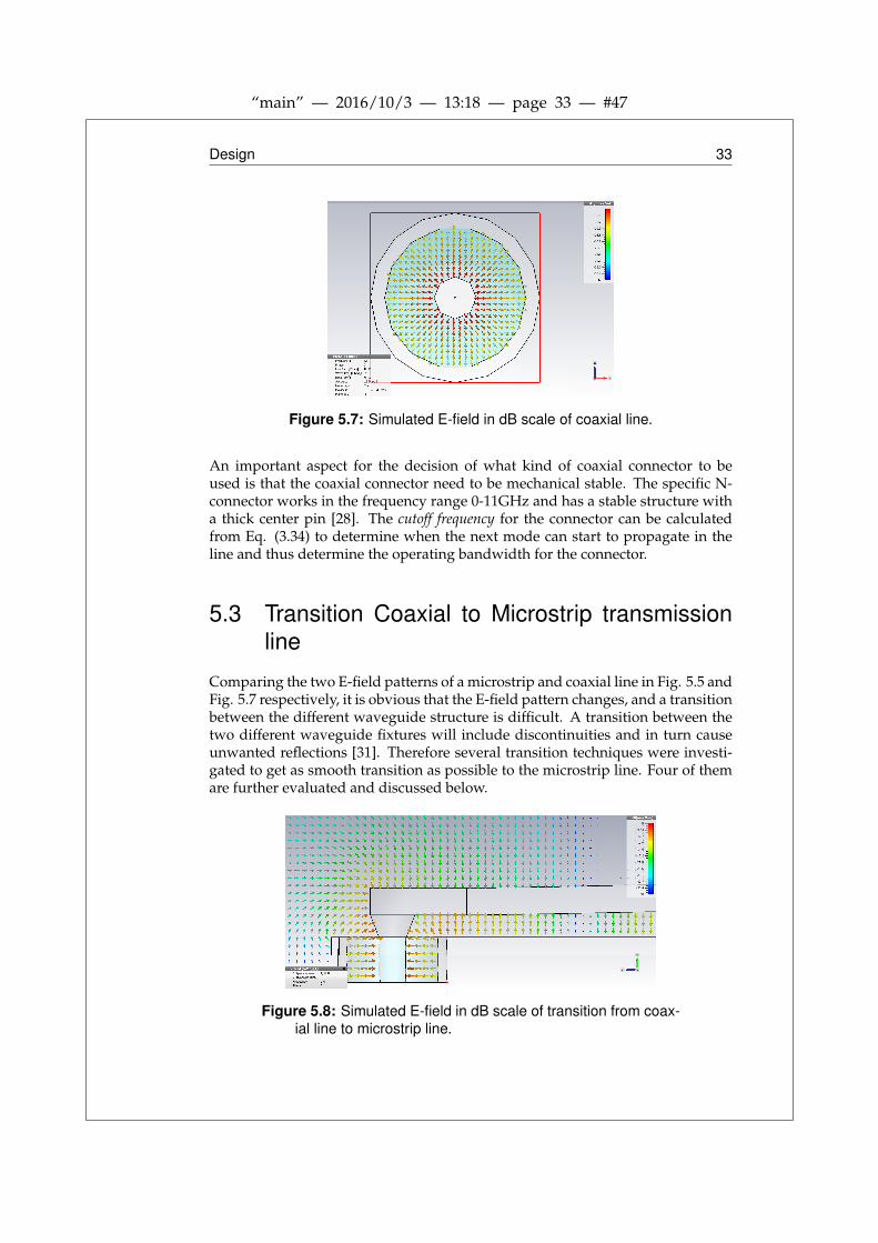
5.3 Microstrip line with bent edges in highlighted shape. . . . . . . . . 315.4 Microstrip line with waveguide ports in CST. . . . . . . . . . . . . . 315.5 Simulated E-field in dB scale of a microstrip line. . . . . . . . . . . 325.6 Coaxial line in highlighted shape. . . . . . . . . . . . . . . . . . . . 325.7 Simulated E-field in dB scale of coaxial line. . . . . . . . . . . . . . 33
vii

“main” — 2016/10/3 — 13:18 — page viii — #10
5.8 Simulated E-field in dB scale of transition from coaxial line to mi-crostrip line. . . . . . . . . . . . . . . . . . . . . . . . . . . . . . . . . 33
5.9 Design of Coaxial connectors A-D. . . . . . . . . . . . . . . . . . . . 345.10 Simulated reflection coefficient S11 for the different coaxial con-
nectors. . . . . . . . . . . . . . . . . . . . . . . . . . . . . . . . . . . 355.11 Simulated transmission coefficient S21 for the different coaxial con-
nectors. . . . . . . . . . . . . . . . . . . . . . . . . . . . . . . . . . . 365.12 Tapered microstrip lines in highlighted shape. . . . . . . . . . . . . 375.13 The planar section, in highlighted shape, covering the test sample. 375.14 The test sample in highlighted shape. . . . . . . . . . . . . . . . . . 385.15 Simulated E-field in dB scale of the TEM cell without the test sample. 385.16 Simulated E-field in dB scale with Teflon as test sample. Width of
test sample 150mm. . . . . . . . . . . . . . . . . . . . . . . . . . . . 395.17 Simulated E-field in dB scale of Teflon as test sample. Width of
test sample 100mm. . . . . . . . . . . . . . . . . . . . . . . . . . . . 395.18 Simulated E-field in dB scale of Teflon as test sample. Width of
test sample 56mm. . . . . . . . . . . . . . . . . . . . . . . . . . . . . 405.19 Simulated Permittivity for teflon as test sample for different widths. 405.20 Ground plane of the fixture in highlighted shape. . . . . . . . . . . . 415.21 Plastic frame with bolts to stabilize and adjust the fixture, in high-
lighted shape. . . . . . . . . . . . . . . . . . . . . . . . . . . . . . . . 415.22 Bolts mounted on top of the structure to adjust the width to height
ratio. . . . . . . . . . . . . . . . . . . . . . . . . . . . . . . . . . . . . 425.23 Simulated reflection coefficient S11 the different setups. . . . . . . . 435.24 Simulated transmission coefficient S21of the different setups. . . . 435.25 Permittivity of Teflon with Baker Jarvis algorithm of the different
setups using simulated data. . . . . . . . . . . . . . . . . . . . . . . 445.26 Permittivity of Rubber with Baker Jarvis algorithm of the different
setups using simulated data. . . . . . . . . . . . . . . . . . . . . . . 455.27 Permittivity of Epoxy Resin with Baker Jarvis algorithm of the dif-
ferent setups using simulated data. . . . . . . . . . . . . . . . . . . 455.28 Permittivity of Lead glass with Baker Jarvis algorithm of the differ-
ent setups using simulated data. . . . . . . . . . . . . . . . . . . . . 465.29 Simulated transmission and reflection of the final design (Setup B). 47
6.1 Manufactured test design with coaxial SMA-connectors. . . . . . . 496.2 Standard female N-connector. . . . . . . . . . . . . . . . . . . . . . 506.3 Manufactured pieces for the transition between the coaxial con-
nector and microstrip. . . . . . . . . . . . . . . . . . . . . . . . . . . 506.4 Manufactured test samples in an unknown material, teflon mate-
rial and bakelite material. . . . . . . . . . . . . . . . . . . . . . . . . 516.5 Saab Aerostructures manufacturing Engineering Short Series Pro-
duction and Spares department. A test sample in bakelite is cur-rently being manufactured in the milling machine to the left. Theauthors are also present in the picture. . . . . . . . . . . . . . . . . 52
6.6 Manufactured final design with an inserted test sample. . . . . . . 536.7 Manufactured final design viewed from above. . . . . . . . . . . . . 53
viii

“main” — 2016/10/3 — 13:18 — page ix — #11
6.8 Manufactured final design viewed from one of the coaxial connec-tors. . . . . . . . . . . . . . . . . . . . . . . . . . . . . . . . . . . . . 54
6.9 Manufactured final design with close up view of the transition fromone of the coaxial connectors. . . . . . . . . . . . . . . . . . . . . . 54
7.1 Measured scattering parameters of the empty TEM cell. . . . . . . 567.2 Numerical scattering parameters of the empty TEM cell. . . . . . . 567.3 Measured permittivity of air. . . . . . . . . . . . . . . . . . . . . . . . 577.4 Measured permittivity of teflon. . . . . . . . . . . . . . . . . . . . . . 587.5 Numerical permittivity of teflon. . . . . . . . . . . . . . . . . . . . . . 597.6 Measured permittivity of bakelite. . . . . . . . . . . . . . . . . . . . 607.7 Numerical permittivity of bakelite. . . . . . . . . . . . . . . . . . . . 607.8 Measured permittivity of an Unknown material. . . . . . . . . . . . . 617.9 Measured scattering parameters of the empty TEM cell. . . . . . . 627.10 Numerical scattering parameters of the empty TEM cell. . . . . . . 637.11 Measured permittivity of Air. . . . . . . . . . . . . . . . . . . . . . . 647.12 Measured scattering parameters of Teflon. . . . . . . . . . . . . . . 657.13 Measured permittivity of Teflon. . . . . . . . . . . . . . . . . . . . . 65
ix

“main” — 2016/10/3 — 13:18 — page x — #12
x

“main” — 2016/10/3 — 13:18 — page xi — #13
List of Tables
5.1 Table of dimensions (in mm) of the different setups A-D. . . . . . . 42
xi

“main” — 2016/10/3 — 13:18 — page xii — #14
xii

“main” — 2016/10/3 — 13:18 — page 1 — #15
Chapter1Introduction
This project aims to explore alternative material characterization measurementsetups using a TEM cell (Transverse ElectroMagnetic cell) that complements andalso simplifies material measurements [1, 2, 3, 4, 5, 6, 7, 8]. The project is car-ried out at Saab which is one of Sweden’s most technology-intensive companiesworking in the defense sector. Saab’s work with avionics, radar applications andstealth technology sets high demands on the knowledge of how the electrical andmagnetic fields behave due to variations of permittivity and permeability of dif-ferent materials. A typical application where the knowledge of the permittivityand permeability is of interest, is when designing materials for fighter jets shownin Fig. 1.1.
Figure 1.1: Jas 39 Gripen, from [43].
Material characterization is a complex and interesting science and the determina-tion of the material properties at microwave-frequencies is challenging. Informa-tion about the permittivity and permeability is of interest in a variety of applica-tions, for example in the communication and military industry. By applying anexternal electromagnetic field on a material sample, material properties can be in-vestigated. To determine how much impact a material has on an electromagnetic
1

“main” — 2016/10/3 — 13:18 — page 2 — #16
2 Introduction
field, one needs to determine the constitutive relations of the material. The per-mittivity ε and the permeability µ are associated with the electric and magneticfields, respectively. Behind the two parameters there are physical explanationswhich are treated in the following chapters.
The basic principle for determining the permittivity and the permeability is tomeasure the reflected and transmitted electromagnetic fields when a materialsample is illuminated with an incident electromagnetic field, as shown in Fig.1.2. This can be done using a free space measurement setup with antennas or byusing guided waves in a waveguide [9].
Figure 1.2: Dielectric slab where E′2+ is the transmitted electricfield from the incident E1+, and E1− is the reflected electricfield.
There is a wide range of techniques used today to determine the constitutive re-lations, and depending on the desired frequency range one needs to considerdifferent kinds of waveguides with specific operating bandwidths. To determinethe operating bandwidth for a waveguide one needs to consider which modes thesystem support. The cutoff frequency determines the frequency at which a modecan propagate and depends on the transverse (orthogonal to the propagation di-rection) components [9]. The lower limit of the operating bandwidth is definedby the cutoff frequency of the first propagating mode and the upper limit is deter-mined from the cutoff frequency of the first higher order mode.
The first mode that can propagate in the system is defined as the lowest prop-agating frequency. This means that the cutoff frequency for the first mode is thelowest frequency where you can transfer a signal with information in the prop-agation direction without that the information get lost due to attenuation, fromthe transmitter to the receiving point in the waveguide. Waveguides also supporthigher order modes and two modes can simultaneously propagate in the waveg-uide. This phenomena is not desirable because one can not determine whichmode is carrying the information and the modes can interfere with each other.
One method used today is the parallel plate capacitor where the permittivity canbe determined for a fixed frequency [10, 11]. This method works good for a fewfrequencies, but gets time consuming while measuring over a larger spectrum.That is when the rectangular waveguide comes into the picture. The rectangular

“main” — 2016/10/3 — 13:18 — page 3 — #17
Introduction 3
waveguides can be used to determine the permittivity and the permeability fora given frequency range [12]. The advantages of this method is that it is easy toinsert a test sample and it generates accurate measurements. This method is aone-conductor system and does only support the TE and TM mode with cutofffrequency fc > 0, which is undesired for lower frequency measurements. Waveg-uides that support TEM modes have the specific characteristic that the lower cut-off frequency is zero [9], which means that they theoretically works for measure-ments from DC.
Two-conductor systems, for example the coaxial waveguide, support TEM modes.The coaxial waveguide has some disadvantages. The test sample is difficult to in-sert into the waveguide and it needs to be perfectly fitted inside the setup to avoidmeasuring errors due to field leakage. Another problem is to know exactly wherethe sample is located within the waveguide, which is important for the calibra-tion where you move the reference plane to the test sample’s surface. To avoidthe disadvantages of the rectangular waveguide where the fundamental modesare the TE or TM mode, a two-conductor system is investigated [13, 14, 15]. Amicrostrip based TEM cell has the advantages that it excites a TEM mode andthat the samples are easy to insert in the TEM cell. The test sample does not needthe same precision of size and shape when manufactured as the case is for thecoaxial line setup.
In this thesis a TEM cell is theoretically investigated, designed and manufac-tured for material characterization. It is similar to the ideas based on the parallelplate waveguide [10, 11, 13]. The fundamental mode for the waveguide is theTEM mode, but the TE and TM modes can also be triggered by the waveguide.The operating bandwidth is determined from the higher order TE or TM modes[16]. Scattering parameters are used to extract material characteristics. The de-sign is investigated in CST, a numerical FDTD solver [17]. The setup is designedto match a 50Ω system.
Two different algorithms, Baker Jarvis [18] and Nicolson-Ross-Weir [19] are usedto calculate the complex permittivity and permeability for the test sample in themicrostrip waveguide [20]. The test sample consist of teflon because of its well-known electromagnetic properties that are defined for a wide range of frequen-cies.
Chapter 2 serves as an introduction to material physics. Chapter 3 highlightsthe fundamentals of electromagnetism and further on dives into the applicationsof electromagnetic waves and how they behave in waveguides and transmissionlines, including different types of impedance matching techniques. Chapter 4 isan introduction to scattering parameters and the simulation and measuring tools.From the information gained from the first 4 chapters, the final design is moti-vated and simulated in chapter 5. Chapter 6, 7 and 8 presents the manufacturedTEM cell, validation and verification of this project, respectively.

“main” — 2016/10/3 — 13:18 — page 4 — #18
4 Introduction

“main” — 2016/10/3 — 13:18 — page 5 — #19
Chapter2Material Characterization
Electromagnetic properties of materials are of interest for scientists as well as forpeople working with applications. There are 102 known elements from which 92can be found in nature [21]. All matter is formed from either one or a combinationof the different elements. An atom consist of protons (positive charged), neutrons(neutral charge) and electrons (negative charge), which can be seen from Bohratom model of a water molecule in Fig. 2.1.
Figure 2.1: Bohr Atom-model of water molecule.
Every element has a number in the periodic system, Fig 2.2, defined from thenumber of protons in the atom.
5

“main” — 2016/10/3 — 13:18 — page 6 — #20
6 Material Characterization
Figure 2.2: Periodic System from [44].
Illuminating a material sample with an external electromagnetic field at for ex-ample microwave frequency, makes the material change the electromagnetic fieldpattern. The displacements of the electromagnetic field pattern is related to thepermittivity and permeability. To characterize the permittivity and permeabilityof a materiel sample the electric and magnetic field are measured, respectively.
2.1 Dielectric MaterialsMaterials were the charges are not free to travel like in conductors, are nameddielectric materials. As an ideal dielectric material has the special characteristicthat it does not contain any free charges and is microscopically neutral as shownin Fig. 2.3.
Figure 2.3: Hydrogen atom.
Applying an external E-field to a dielectric material makes the bound chargesmove slightly relative to each other meaning that the centroids of the charge dis-tribution shift slightly from the initial positions. In a perfect conductor on theother hand which only contains free charges,the free charges moves the surfaceof the material. The movement of the centroids relative to its initial state in the

“main” — 2016/10/3 — 13:18 — page 7 — #21
Material Characterization 7
atom creates numerous electric dipoles. Movement due to an applied externalfield of the small group of dielectric dipole in a material is called polarization [21].The polarization due to the electric field alters the ability of the material to storeelectric energy. It is analogous to the potential energy stored in a spring stretch-ing it a length from its initial state. There are three kinds of polarization; dipole ororientational polarization, where the dipole tends to align with the applied field,ionic or molecular polarization that contains positive and negative ions which dis-places themselves due to the applied field. The third and the last polarization typeis named electronic polarization and is the most usual behavior of material wherethe applied field displaces the electric cloud center of the atom relative to the cen-ter of the nucleus. The polarization phenomena gives rise to the potential energystored in the material. To determine the static permittivity, a simple parallel plateconductor can be used. By determining the polarization vector P with the testsample between the parallel plate conductor and relate it to the case where theconductor contains only vacuum, the relative permittivity is defined in Eq. (2.1)[21].
εsr =
εs
ε0(2.1)
Where ε0 = 8.854 · 10−12[F/m] is the permittivity in vacuum and εs is the mea-sured permittivity of the sample. The relative permittivity εsr defines the chargestorage capacity of a dielectric material relative to vacuum.
2.2 Magnetic MaterialsA material with magnetic characteristics displays magnetic polarization whenthe material is exposed to an external magnetic field. It is not trivial to examineand understand the macroscopic behavior of magnetic material where quantumtheory is applied. In this thesis we only treat dielectrics and will only mentionthat the relative permeability is defined as [21]
µsr =
µs
µ0(2.2)
where µ0 is the permeability in vacuum and µs is the measured permittivity ofthe sample.
2.3 Complex Permittivity and PermeabilityTo determine the permittivity of dielectric materials where the frequency depen-dence is considered, the complex permittivity is defined as ε = ε′ − jε′′ (2.3)
Complex permittivity is written with a real part and an imaginary part. The realpart Re(ε) = ε′ gives the relative permittivity of the dielectric material while

“main” — 2016/10/3 — 13:18 — page 8 — #22
8 Material Characterization
the imaginary part Im(ε) = ε′′ defines the losses of the material. The effectiveelectric losses are sometimes given as the electric loss tangent. The electric losstangent is defined by
tan σe =ε′′ε′ (2.4)
The complex permeability is defined in a similar way. µ = µ′ − jµ′′ (2.5)
There are different kinds of magnetic materials. Diamagnetic, paramagnetic andantiferromagnetic materials almost have the same relative permeability as vac-uum µ0. But for material with high permeability for example ferromagnetic andferrimagnetic materials there is a loss tangent introduced. The loss tangent is ameasure of the magnetic losses and is described by Eq. (2.6).
tan σm =µ′′µ′ (2.6)
2.4 Transmission/Reflection Method toestimate material parameters
There are a range of different techniques to determine the material parameterssuch as, reflection methods, transmission/reflection methods, resonator methodsand planar-circuit methods (just to name a few) [11, 22, 23]. The method used inthis project is the transmission/reflection method. To determine the permittiv-ity and/or permeability of the test sample, the material is placed in a waveguidefixture (for example in a coaxial line or in a microstrip line) and the scattering pa-rameters are measured. To determine the material parameters, the scattering pa-rameters are inserted in an algorithm where the required information is extractedand the desired material parameters are derived. There are several methods todetermine the material parameters because when performing the transmissionand reflection method the system of equations is generally over-determined. Twodifferent methods, Nicolson-Ross-Weir [19] and Baker Jarvis [18] are examinedand applied in this project.
2.4.1 Nicolson-Ross-Weir AlgorithmTo explicitly determine the permittivity and permeability the Nicolson-Ross-Weiralgorithm [19, 22] can be used. The algorithm uses the scattering parameterswhere both the measured reflection S11 and transmission S21 parameters are used[19]. Γ is the reflection coefficient which can be described by
Γ = K±√
K2 − 1 (2.7)
where

“main” — 2016/10/3 — 13:18 — page 9 — #23
Material Characterization 9
K =
(S2
11 − S221)+ 1
2S11(2.8)
To determine the sign of Eq. (2.7), gamma is required to be |Γ| ≤ 1. The transmis-sion coefficient T is defined by
T =(S11 − S21)− Γ
1− (S11 + S21) Γ(2.9)
By using the equation above the permittivity ε and the permeability µ are de-scribed by Eq. (2.10) and (2.11) respectively.
µr =1 + Γ
(1− Γ)Λ√
1λ2
0− 1
λ2c
(2.10)
εr =λ2
o
µr
(1
λ2c− 1
Λ2
) (2.11)
where λc is the cutoff wavelength of the transmission line. λ0 is defined as the freespace wavelength in vacuum. Λ is defined by
1Λ2 = −
[1
2πDln(
1T
)](2.12)
where D is the thickness of the sample.
The phase shift needs to be taken into account for the algorithm to work properly,because of the distance between the excitation point and the material placement.This can be done by calibrating to the reference plane and calculating the phaseshift and assuming that the phase shift between every two frequency points con-secutive is less than 2π [19].
2.4.2 Baker JarvisDepending on the type of waveguide fixture used, the scattering parameters havean important role in determining the material parameters. For waveguides witha certain reflection parameter over a measured frequency range, the reflection co-efficient can interfere with the measurement resulting in inaccurate permittivityand permeability. The problems of the Nicolson-Ross-Weir algorithm is to com-pensate for the phase delay and that it does not work well for frequencies wherethe test sample length is a multiple of a half a wavelength [22]. For frequencieswhere the material thickness is a multiple of half a wavelength, the scatteringparameter |S11| becomes almost zero and the algorithm gets algebraically unsta-ble. Baker Jarvis is an algorithm where the transmission parameters S21 and S12are taken into account and the reflection parameters S11 and S22 can be weightedwith α, depending on the accuracy of the input data. Baker Jarvis, Eq. (2.13), is
“main” — 2016/10/3 — 13:18 — page 10 — #24
10 Material Characterization
an iterative algorithm [22, 24, 25] where the sample length and the position of thereference plane needs to be accurately known.
1
2[(S12 + S21) + α (S11 + S22)] =
T(1− Γ2)+ αΓ
(1− T2)
1− P2Γ2(2.13)
α is a weighting factor and can be adjusted depending on the loss factor of the ma-terial. The propagating term with calibration of the reference plane, P = e−jkmd,where km = k0
√εrµr and d is the thickness of the test sample. For a low loss
material, α can be set to zero because the transmission parameter S21 is good. Ingeneral, the uncertainty of the method increases for high loss materials.
“main” — 2016/10/3 — 13:18 — page 11 — #25
Chapter3Waveguide Theory
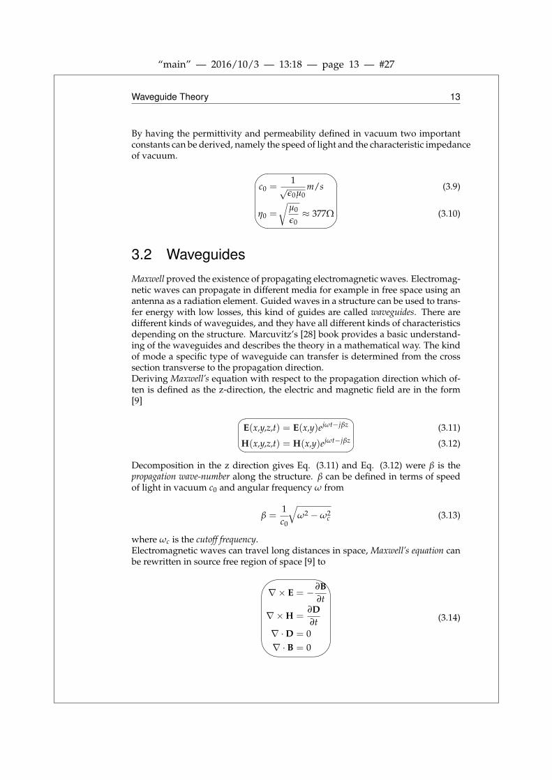
Classical electromagnetic theory describes the electric and magnetic phenomenain nature. James Clerk Maxwell (1831-1879) used four fundamental equations (3.1)to describe all electromagnetic phenomena in an accurate and elegant way [9, 26,27].
∇× E = −∂B∂t
∇×H = J +∂D∂t
∇ ·D = ρ
∇ · B = 0
Maxwell′s equations (3.1)
The electric field E and the magnetic field H are measured in [Volt/m] and [Am-pere/m], respectively. Electric flux density D and the magnetic flux density B aremeasured in [Coulomb/m2] and [Weber/m2] or [Tesla]. Electric displacement andmagnetic induction is another word for D and B. The two last quantities are thevolume charge density ρ and the electric current density measured in [Coulomb/m3]and [Ampere/m2], respectively [21].
Maxwell unified observations made by Michael Faraday (1791-1867), Karl Fried-richGauss (1777-1855) and Andre-Marie Ampere (1775-1836). Maxwell completed Am-pere’s law with the displacement current ∂D/∂t which is fundamental to provethe existence of propagating electromagnetic waves. Maxwell realized that to pre-serve the law of charge conservation the displacement current was the missingingredient to interlink the four equations together [9]. To derive Maxwell’s dis-placement current the divergence is taken of both sides of Ampere’s law and byusing Gauss’s law (3.2) and the vector identity (3.3)
∇ · ∇×H = 0 (3.2)
and∇ ·D = ρ (3.3)
we obtain:
11

“main” — 2016/10/3 — 13:18 — page 12 — #26
12 Waveguide Theory
∇ · ∇×H = ∇ · J +∇ · ∂D∂t
= ∇ · J + ∂
∂t∇ ·D = ∇ · J + ∂p
∂t
and by using the vector identity from Eq. (3.2), the law of charge conservation isderived.
∂ρ
∂t+∇ · J = 0 charge conservation (3.4)
The charge conservation is an important law which is always true for a closedsystem. An analogy to charge is energy where energy cannot disappear or becreated out of nothing. Energy can only transform into different kind of energyforms. The same applies to charge, it can not vanish or be created from nothing.Charge varies in regions of space because it travels between different regions.The law of charge conservation also states that charges in good conductors almostinstantaneous move to the surface of the conductor and distribute itself to reachcharge equilibrium at the surface of the structure[27].
3.1 Constitutive relations
Applying an electric or magnetic field to different kind of materials changes theelectric and magnetic field pattern [21]. The constitutive parameters of linearmaterials are not a function of the applied field, otherwise they are nonlinear ma-terials. Many materials have linear characteristics as long as the applied fieldsare within certain limits. When the constitutive parameters are not a function ofposition, the media is called homogeneous and otherwise in-homogeneous. Allmedia have some degree of non-homogeneity, but if small, they are seen as homo-geneous. Dispersive media is the case when the constitutive parameters dependson the frequency. When the constitutive parameters vary with the direction of theapplied field the media is called non-isotropic otherwise it is called isotropic[21].There exists a fundamental connection between the electric D and magnetic Bflux densities which is related to the electric field E and magnetic field H respec-tively. Eq. (3.5) and Eq. (3.6) gives the relation between flux and field intensitiesin vacuum [9].
D = ε0EB = ε0H
(3.5)(3.6)
ε0 is the permittivity of free space measured in [Farad/m] and µ0 is the perme-ability of free space measured in [Henry/m]. The physical constants have thenumerical values:
ε0 ≈ 8.854 · 10−12F/m
µ0 = 4π · 10−7H/m
(3.7)
(3.8)
“main” — 2016/10/3 — 13:18 — page 13 — #27
Waveguide Theory 13
By having the permittivity and permeability defined in vacuum two importantconstants can be derived, namely the speed of light and the characteristic impedanceof vacuum.
c0 =
1√
ε0µ0m/s
η0 =
õ0
ε0≈ 377Ω
(3.9)
(3.10)
3.2 WaveguidesMaxwell proved the existence of propagating electromagnetic waves. Electromag-netic waves can propagate in different media for example in free space using anantenna as a radiation element. Guided waves in a structure can be used to trans-fer energy with low losses, this kind of guides are called waveguides. There aredifferent kinds of waveguides, and they have all different kinds of characteristicsdepending on the structure. Marcuvitz’s [28] book provides a basic understand-ing of the waveguides and describes the theory in a mathematical way. The kindof mode a specific type of waveguide can transfer is determined from the crosssection transverse to the propagation direction.Deriving Maxwell’s equation with respect to the propagation direction which of-ten is defined as the z-direction, the electric and magnetic field are in the form[9]
E(x,y,z,t) = E(x,y)ejωt−jβz
H(x,y,z,t) = H(x,y)ejωt−jβz
(3.11)
(3.12)
Decomposition in the z direction gives Eq. (3.11) and Eq. (3.12) were β is thepropagation wave-number along the structure. β can be defined in terms of speedof light in vacuum c0 and angular frequency ω from
β =1c0
√ω2 −ω2
c (3.13)
where ωc is the cutoff frequency.Electromagnetic waves can travel long distances in space, Maxwell’s equation canbe rewritten in source free region of space [9] to#
"
!
∇× E = −∂B∂t
∇×H =∂D∂t
∇ ·D = 0∇ · B = 0
(3.14)
“main” — 2016/10/3 — 13:18 — page 14 — #28
14 Waveguide Theory
The Fourier transform of the derivative gives the relation jω ⇔ ∂∂t . Combining
the Fourier transform of a derivative and the constitutive relations (3.5) and (3.6),Eq. (3.15) can be described by Maxwell’s equation at a source-free region:
∇× E = −jωµH∇×H = jωµE∇ · E = 0∇ ·H = 0
(3.15)
Decomposing Maxwell’s equation in the guiding direction (z direction) and thetransverse directions (x,y directions) and assuming that the medium in which thewave propagates is loss-less, Eq. (3.16) can be described by [9].
∇TEz × z− jβz× ET = −jωµHT
∇T Hz × z− jβz×HT = jωεET
∇T × ET + jωµzHz = 0∇T ×HT − jωεzEz = 0∇T · ET − jβEz = 0∇T ·HT − jβHz = 0
(3.16)
where ∇T is the differential operator in the tangential plane.Depending on how the electric and magnetic component varies in the transverse(x,y direction) and the z-direction, different modes can be defined.
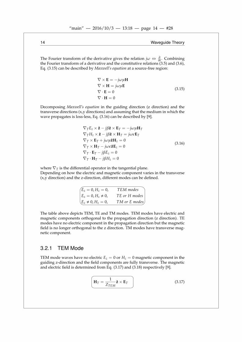
Ez = 0, Hz = 0, TEM modesEz = 0, Hz , 0, TE or H modesEz , 0, Hz = 0, TM or E modes
The table above depicts TEM, TE and TM modes. TEM modes have electric andmagnetic components orthogonal to the propagation direction (z direction). TEmodes have no electric component in the propagation direction but the magneticfield is no longer orthogonal to the z direction. TM modes have transverse mag-netic component.
3.2.1 TEM Mode
TEM mode waves have no electric Ez = 0 or Hz = 0 magnetic component in theguiding z-direction and the field components are fully transverse. The magneticand electric field is determined from Eq. (3.17) and (3.18) respectively [9].
HT =
1ZTEM
z× ET (3.17)
“main” — 2016/10/3 — 13:18 — page 15 — #29
Waveguide Theory 15
where ZTEM =√
µε is the characteristic impedance.
∇T × ET = 0∇T · ET = 0
(3.18)
Waveguides which support TEM mode propagation have the properties that thecutoff frequency fc = 0 or equivalent with the cutoff wavenumber kc = 0. The waveimpedance of a TEM mode is the same as for a plane wave in a lossless medium[29] and is determined from
ZTEM =|ET ||HT |
=ωµ
β=
õ
ε(3.19)
where the wave impedance is a function of the transverse field components andmaterial constants. TEM modes can only propagate in two or higher order con-ductor system [26].
3.2.2 TE ModeWhen Ez = 0 and Hz , 0 the mode is named TE mode. It implies that themode can have a magnetic component in the propagation direction. Eq. (3.20)determines all the field components for the TE modes.
∇2
T Hz + k2c Hz = 0
HT = − jβk2
c∇T HZ
ET = ZTEHT × z
(3.20)
The TE wave impedance is determined from
ZTE =Ex
Hy=−Ey
Hx=
ωµ
β(3.21)
were β is the index of the mode discussed in the beginning of this chapter. ZTE isfrequency dependent and the TE mode can propagate both in a closed conductoras well as in a two or higher order conductor system [26].
3.2.3 TM ModeUnlike the TE mode the TM mode have Hz = 0 and Ez , 0. To determine thefield component for the TM mode the equation (3.22) applies.#
"
!
∇2TEz + k2
c Ez = 0
ET = − jβk2
c∇TEZ
HT =1
ZTMz× ET
(3.22)

“main” — 2016/10/3 — 13:18 — page 16 — #30
16 Waveguide Theory
The TM wave impedance is determined from
ZTM =Ex
Hy=−Ey
Hx=
β
ωε=
βzk
(3.23)
As for the TE case , ZTM is also frequency dependent, and the TM mode canbe triggered in closed conductor as well as in a two or higher order conductorsystem[26].
3.2.4 Operating BandwidthThe operating bandwidth varies depending on the kind of waveguide systemused. Typically for a TEM waveguide the lowest theoretically possible propaga-tion mode starts at DC which means that the lowest mode has no cutoff frequency.It is possible for higher order modes to propagate in waveguides depending onthe geometry of the fixture. The upper frequency limit is determined by the cutofffrequency of the next higher order mode. If a signal is transmitted, it is importantto know which mode is carrying the signal to avoid distortion and dispersion.The operating frequency interval, ω, can be defined as [9]
ωc1 < ω < ωc2 (3.24)
where ωc1 is the cutoff frequency for the used mode and ωc2 is the cutoff frequencyof the next higher order mode.
TE and TM modes defines the upper limit of the usable bandwidth in a TEMwaveguide. TE and TM modes have a lower limit for the cutoff frequency whichcannot be zero. Coaxial cable is a typical example of a TEM waveguide wherethe operating bandwidth is defined from DC to the first higher order propaga-tion mode [9]. The operating bandwidth of a transmission line will be discussedfurther in section 3.5.
3.3 Transmission lineStructures designed to transmit a signal with information or power from pointa to point b are the definition of a transmission line [30]. The transmission lineis designed to carry Transverse ElectroMagnetic (TEM) waves in a given direc-tion often denoted the ±z direction, where z is the propagation direction alongthe structure. Different kinds of transmission lines exists, such as parallel platewaveguides, microstrip lines and coaxial lines which are described below.
3.4 Characteristic impedanceThe characteristic impedance of a transmission line is given by Eq. (3.25), whichdepends on the line geometry and the material of which the wave is propagating[29].

“main” — 2016/10/3 — 13:18 — page 17 — #31
Waveguide Theory 17
Z0 =V0
I0(3.25)
where V0 is the incident voltage and I0 is the incident current.
3.5 Higher order modes
The cutoff frequency is defined as the frequency at which the mode can start topropagate in the transmission line. Undesirable effects can occur if two or moremodes with different propagation constants are propagating at the same time.Typically for a transmission waveguide several modes that propagate at the sametime affect each other by distortion and dispersion. This causes problem becausethe actual mode that is carrying the transmitted signal may become unknown.
3.6 Parallel Plate Waveguide
A parallel plate waveguide consists of two parallel plates which are used for lowloss transmissions of signals at microwave frequencies. The conducting platesare separated by a distance h, as shown in Fig. 3.1. The gap between the twoplates can be filled with a dielectric material with permittivity ε and permeabilityµ0. The strip width w of the plates is often assumed to be much greater than theseparation h. This results in a sufficiently small variation in x which implies thatthe fringing field outside the waveguide, described more in section 3.6, can beignored.
Figure 3.1: E- and H-fields of a parallel Plate transmission line.
The electric and magnetic fields propagate inside the waveguide in y respectivex direction. They can be seen as vector components according to the Helmholtzequation [29] which is a reduced form of the Maxwell’s equation. ∇2E + k2E = 0 (3.26)
where the constant k = ω√
µε is defined and called the wave number.

“main” — 2016/10/3 — 13:18 — page 18 — #32
18 Waveguide Theory
3.7 Microstrip lineA microstrip line, as shown in Fig. 3.2a, is a type of planar transmission linewhere a conductor of width w is printed on a thin, grounded dielectric substrate[31]. The substrate, of thickness h, is placed between the microstrip and groundplane and has the relative permittivity εr. As can be seen in Fig. 3.2b, because ofthe sufficiently small width w of the strip compared to the ground plane width,there is a field outside the waveguide called the fringing field that must be takeninto account. In this thesis the dielectric is defined as air, which leads to thatthe microstrip is embedded in air. This constitutes a simple TEM transmissionline. For a dielectric with εr > 1, the microstrip can no longer support a pureTEM wave. The simple explanation is that the phase velocity for the wave is notthe same in air as in the dielectric medium, and the wave becomes a quasi-TEMmode [29]. This complicates the calculations and needs more advanced analysistechniques to understand the phenomena.
Figure 3.2: E-, H- and fringing fields of a microstrip transmissionline.
3.7.1 Characteristic Impedance of a microstrip lineThe characteristic impedance can be calculated in several ways. Some of the mostaccurate one is the Hammerstad and Jensen’s [32] where Z0 can be calculated ac-cording to Eq. (3.27).
Z0 =
n0
2π√ee f f
ln
(f (u)
u+
√1 +
4u2
)(3.27)
where
f (u) = 6 + (2π − 6)
(−[
30.666u
]0.7528)
and
u =wh

“main” — 2016/10/3 — 13:18 — page 19 — #33
Waveguide Theory 19
The effective dielectric constant εe f f is calculated by
εe f f =εr + 1
2+
εr − 12
(1 +
10u
)−ab(3.28)
where
a = 1 +149
ln[
u4 + (u/52)2
u4 + 0.432
]+
118.7
ln[
1 +( u
18.1
)3]
and
b = 0.564(
εr − 0.9εr + 3
)0.053
Another way to estimate the characteristic impedance [29] is
Z0 =
60√εe
ln( 8u + u
4 ) f or u ≤ 1120π√
εe f f1
(u+1.393+0.667 ln (u+1.444)) f or u ≥ 1(3.29)
According to Kraus [33], the impedance for a microstrip line can be found as
Z0 =η0√
εr[u + 2](3.30)
where η0 is the wave impedance of free space and εr the relative permittivity ofthe dielectric material between the microstrip and ground plane.As can be seen in Fig. 3.3, the characteristic impedance is plotted for the threeequations as a function of u.

“main” — 2016/10/3 — 13:18 — page 20 — #34
20 Waveguide Theory
1 2 3 4 5 6 7 8
u
30
40
50
60
70
80
90
100
110
120
130
Z / o
hm
Characteristic Impedance
H&J
Kraus
H
Figure 3.3: Characteristic impedance Z0 of a microstrip line as afunction of u = w/h (width/height ratio). Hammerstad andJensen (red line) from eq. (3.27), Hammerstad (blue dottedline) from Eq. (3.29) and Kraus (green line) from Eq. (3.30).
3.7.2 Higher order modes and operating bandwidth of a mi-crostrip line
For the microstrip line there exist TM and TE modes with higher order modes.The first higher order mode is the TE11, where the cutoff wavelength and cutofffrequency of the higher order modes [9] can be calculated from Eq. (3.31).
λc = 1.873π
2(a + b)
fc =c
λc=
c0
nλc
(3.31)
Thus, the operating range of the frequency for the TEM mode in a microstrip lineis limited to frequencies smaller than fc, which in turn implies that the operatingbandwidth is limited by the geometry of the microstrip.
3.8 Coaxial LineThe coaxial line consists of two concentric conductors of inner and outer radius aand b respectively, shown in Fig. 3.4, and is the most widely used TEM transmis-sion line. It is designed with a dielectric between the conductors with a dielectricmaterial such as polyethylene or teflon [29].

“main” — 2016/10/3 — 13:18 — page 21 — #35
Waveguide Theory 21
Figure 3.4: E-, H-field of a coaxial transmission line.
The characteristic impedance in a coaxial line [29] can be calculated from
Z0 =
η0
2πln(
ba
)(3.32)
where
η0 =
õ0
εr(3.33)
3.8.1 Higher order modes and operating bandwidth of a coax-ial line
For the coaxial line there can also exist TM and TE modes, where the TE mode isthe dominant one. The dimensions of the coaxial cable sets an upper limit of thefrequency where TE11 mode and higher order modes starts to propagate. Thisfrequency is the cutoff frequency for the coaxial cable and sets an upper limit of theoperating frequency. The cutoff frequency [29] can be calculated from Eq. (3.34).
fc =ckc
2π√
εr(3.34)
where
kc =2
a + b(3.35)
3.9 Impedance matchingImpedance matching includes various techniques to maximize the transmittedpower or minimize the reflections in a system with electrical signals [30]. Forthe TEM cell, two transitions from coaxial connector to microstrip line need tobe taken into account, and that is when the impedance matching comes into thepicture. Impedance matching is also considered when making a transition from

“main” — 2016/10/3 — 13:18 — page 22 — #36
22 Waveguide Theory
a small microstrip to a larger, which is done with tapering technique. To mini-mize the reflections in a system, this can be achieved when the load impedanceconverges to the characteristic impedance. For reflection less matching, the loadimpedance is equal to the characteristic impedance of the transmission line. Thesetechniques are widely used in this project as there is various physical transitionsthat need to be taken into account.
3.10 TaperingThere are a lot of ways to change the electromagnetic properties in a waveguidesuch as the characteristic impedance, for example by tapering a microstrip line.This is a way to match the desired bandwidth to a specific impedance, by usingmultisection matching transformers. The geometry of a tapered line, as can beseen in Fig. 3.5a, is created by N sections divided over the strip line, Fig. 3.5b.The wideband impedance transformers can typically be realized in three differenttaper setups. Two of them are used in this project, namely the exponential taperand the Klopfenstein taper. These different types of taper methods can be usedto obtain different passband characteristics and are treated in chapter 5 whiledesigning the tapering parts of the TEM cell.
Figure 3.5: Tapering of a transmission line. (a) The tapering andtransformation of impedance Z. (b) The tapering step andimpedance transform from Z to Z + ∆Z.
The total reflection coefficient at z = 0 can be found as
Γ(Θ) =12
∫ L
z=0e−2jβz d
dzln(
ZZ0
)dz (3.36)
where θ = 2βl. By taking the inversion of Γ, the Z(z) can be found. This is kindof difficult and often avoided. Instead different types of cases are specified whereZ(z) is given by an equation [30].

“main” — 2016/10/3 — 13:18 — page 23 — #37
Waveguide Theory 23
3.10.1 Exponential taperFor an exponential taper, Z(z) is described by
Z(z) = Z0eaz f or 0 < z < L (3.37)
To determine the constant a, we begin by calculating Z(z) = Z(0) = Z0. Forz = L, Z(L) = ZL = Z0eaL. This gives a expressed in ZL and Z0 as
a =1L
ln(
ZLZ0
)(3.38)
By using Eq. (3.37) it follows that
Γ =12
∫ L
0e−2jβz d
dz(ln eaz)dz
=ln(ZL/Z0)
2L
∫ L
0e−2jβzdz
=ln(ZL/Z0)
2e−jβL sin βL
βL
(3.39)
where β is the propagation constant and L as indicted in Fig. 3.6.
Figure 3.6: Exponential tapering of a transmission line. (a) Thetapering and transformation of impedance. (b) Resulting re-flection of a matching section.

“main” — 2016/10/3 — 13:18 — page 24 — #38
24 Waveguide Theory
3.10.2 Klopfenstein taperThe Klopfenstein taper is a method used in designing connectors, and can alsobe seen as the optimum tapering method for the microstrip line section of theTEM cell, with respect to low reflection coefficient over the passband for a giventapering length [29, 30, 34]. It is described by a stepped Chebyshev transformerwhere the number of sections increases to infinity.The logarithmic characteristic impedance is given by the following equation.
ln Z(z) =12
Z0ZL +Γ0
cosh AA2φ
(2zL− 1, A
)f or 0 ≤ z ≤ L (3.40)
where
φ(x, A) = −φ(−x, A) =∫ x
0
I1(A√
1− y2
A√
1− y2dy f or|x| ≤ 1 (3.41)
which is a defined function of x and A where I1 is the modified Bessel function.Eq. (3.41) has some special cases with the following values in (3.42).
φ(0, A) = 0
φ(x, 0) =x2
φ(1, A) =cosh A− 1
A2
(3.42)
Besides these special cases, Eq. (3.41) needs to be calculated numerically. Theconcept is used when designing the tapered sections of the waveguide setup.

“main” — 2016/10/3 — 13:18 — page 25 — #39
Chapter4Simulation and measuring tools
4.1 Scattering parametersThe scattering parameters (S-parameters) are a measure of transmitted and re-flected amplitude of the signal and describe the electric behavior in a linear two-port network [9]. The S-parameters are essential for a measuring setup such asthe TEM cell. A typical TEM cell is characterized as a two-port with circuit pa-rameters as seen in Fig. 4.1, where the incoming waves a1 and a2 relate to theoutgoing waves b1 and b2, respectively. For the respective ports, the transmittedsignal are denoted with S12, S21 and reflected signal S11, S22.
Figure 4.1: Scattering parameters for a two-port, from [45].
The transfer matrix ABCD at port 1 which relates the voltage and current to port2 is written as [9]:[
V1I1
]=
[A BC D
] [V2I2
](trans f er matrix) (4.1)
The impedance and admittance matrix relates the total voltages and currents onthe ports, where the impedance matrix is shown in Eq. (4.2). The admittance iscalculated by taking the inverse of the impedance matrix.[
V1V2
]=
[Z11 Z12Z21 Z22
] [I1−I2
](impedance matrix) (4.2)
25

“main” — 2016/10/3 — 13:18 — page 26 — #40
26 Simulation and measuring tools
The transfer and impedance matrices is often denoted T respective Z, where:
T =
[A BC D
], Z =
[Z11 Z12Z21 Z22
](4.3)
The outgoing waves b1 and b2 can be calculated by multiplying the incomingwave parameters a1 and a2 with the scattering matrix in Eq. (4.4), and thus relatesthe incoming wave with the outgoing wave.[
b1b2
]=
[S11 S12S21 S22
] [a1a2
], S =
[S11 S12S21 S22
](scattering matrix) (4.4)
where the traveling wave variables are defined by
a1 =V1 + Z0 I1
2√
Z0a2 =
V2 − Z0 I2
2√
Z0
b1 =V1 − Z0 I1
2√
Z0b2 =
V2 + Z0 I2
2√
Z0
(4.5)
4.2 Simulation ProcedureThe simulation procedure consist of the two numerical programs CST (Computersimulation technology) and Matlab. CST is a numerical simulation tool which isused to solve Maxwell’s equations. It is a cad-based program that has been usedin this thesis to draw parallel plate lines, microstrip lines and coaxial waveg-uides with different dimensions and dielectric materials to simulate the charac-teristic impedance. Matlab was used as a support while comparing the theorywith the simulated results in CST, mainly for numerical calculations of charac-teristic impedance of microstrip and coaxial cables used in modeling the TEMcell. Further on, Matlab is used to run the Nicolson-Ross Weir and Baker Jarvisalgorithm, described in section 2.4, to determine the constitutive variables for dif-ferent types of material.
Four different designs of coaxial connectors have been developed and simulatedto get the best transition for the TEM cell with respect to low reflection and hightransmission. To decide which connector that was most suitable for the TEM cell,the E-field patterns and the S-parameters were studied. The program offers simu-lation in both frequency and time domain to compare the results. Different typesof ports, waveguide port, discrete port and lumped element were used to studyvarious types of transmission signals through the system.
The TEM cell was parameterized so that every parameter could be optimizedby the CST optimizer that uses the Trust Region Framework algorithm to findthe most suitable values. Several simulations were made to optimize it for max-imum transmission, minimum reflection and for combinations of the two. Thesimulated data was exported into Matlab in a Touchstone file to be able to run
“main” — 2016/10/3 — 13:18 — page 27 — #41
Simulation and measuring tools 27
the Nicolson-Ross-Weir and Baker Jarvis algorithm. This gave some interestingresults of how the transmission and reflection parameters affect the resulting sim-ulated electromagnetic variables of different types of material, which is evaluatedin chapter 5.
4.3 MeasurementsThe ASTM standards is a collection of international technical standards for mate-rials, products and systems, just to name a few. The publishing work and devel-opments is voluntarily produced for the public. ASTM international [12, 35] hasa standard test method for measuring relative complex permittivity and perme-ability for different kind of waveguide structures which is of value in this thesis.Setups and procedures must be the same for each measurement to achieve credi-ble results.
4.3.1 Network AnalyzerA network analyzer is an instrument that can be used when analyzing an electri-cal circuit. When working at higher frequency, voltage and current do not serve asa reliable measure. To perform accurate measurement at higher frequency reflec-tion and transmission are used. The VNA (vector network analyzer) measuresthe S-parameters which give information about amplitude and phase. For thisthesis the VNA is used for two-port measuring because the TEM cell can be elec-trically seen as a two-port. Calibration is performed to handle the phase velocityvariations of the excited wave. The calibration is necessary because one needsto change the reference plane to the test samples surface and to eliminate signalswhich are not generated by the test sample. Length of the cable and the transitionbetween the different connectors contributes to the losses.
4.3.2 Extracting the complex permittivity and permeabilityTo calculate the constitutive parameters a Touchstone file or a s2p file is createdfrom the network analyzer. The files are loaded in Matlab using a script whichthen processes the loaded data using the algorithms and plots the result. Theplots depict the real part of the complex permittivity and the imaginary part of thecomplex permittivity. The real part of the complex permittivity gives the relativepermittivity of the test sample while the imaginary part displays the electric lossof the test sample.

“main” — 2016/10/3 — 13:18 — page 28 — #42
28 Simulation and measuring tools

“main” — 2016/10/3 — 13:18 — page 29 — #43
Chapter5Design
Considering the requirements for the measurement setup and the theory fromchapter 1-4, a number of decisions were made for the final design. The decisionsmade for the design procedure are motivated and substantiated with the infor-mation given in the theory part and the specification of the design given in thelist below.
• Frequency range 0-5GHz
• TEM waveguide fixture
• Easy setup for test sample compared to other existing solutions
• 2-port system with input impedance to match 50Ω
The design specification requires that the waveguide is a two-conductor systemwhich support TEM waves. TEM waves support the required fc = 0 whichmeans that the lowest propagation mode in the fixture is defined from 0Hz.
Figure 5.1: Final design with inserted test sample.
The difficult part of the design decision is the fact that the equations for the mi-crostrip waveguide is assumed to have a dielectric material between the groundplane and the conductor. The formula defined for the microstrip impedance, Eq.
29
“main” — 2016/10/3 — 13:18 — page 30 — #44
30 Design
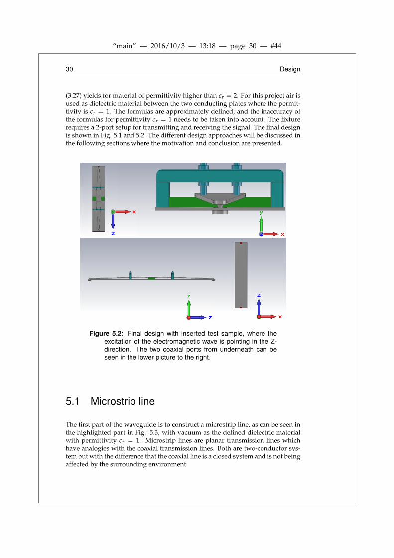
(3.27) yields for material of permittivity higher than εr = 2. For this project air isused as dielectric material between the two conducting plates where the permit-tivity is εr = 1. The formulas are approximately defined, and the inaccuracy ofthe formulas for permittivity εr = 1 needs to be taken into account. The fixturerequires a 2-port setup for transmitting and receiving the signal. The final designis shown in Fig. 5.1 and 5.2. The different design approaches will be discussed inthe following sections where the motivation and conclusion are presented.
Figure 5.2: Final design with inserted test sample, where theexcitation of the electromagnetic wave is pointing in the Z-direction. The two coaxial ports from underneath can beseen in the lower picture to the right.
5.1 Microstrip line
The first part of the waveguide is to construct a microstrip line, as can be seen inthe highlighted part in Fig. 5.3, with vacuum as the defined dielectric materialwith permittivity εr = 1. Microstrip lines are planar transmission lines whichhave analogies with the coaxial transmission lines. Both are two-conductor sys-tem but with the difference that the coaxial line is a closed system and is not beingaffected by the surrounding environment.

“main” — 2016/10/3 — 13:18 — page 31 — #45
Design 31
Figure 5.3: Microstrip line with bent edges in highlighted shape.
The microstrip line is matched to 50Ω where the width to height ratio is funda-mental for the matching. Eq. (3.27) gives an approximate value of the characteris-tic impedance of the microstrip. By numerical simulation, a first approximation ofa thin microstrip is calculated. Fig. 5.4 shows a simplified model with permittiv-ity εr = 1 and waveguide ports to analyze how the impedance varies dependingon different width to height ratio. The operating bandwidth is set by the cutofffrequency for the higher order mode which propagates from around 13GHz. Thiswas determined from Eq. (3.31). The planar section of the TEM cell, which is alsoa kind of microstrip line, is treated and evaluated in section 5.5.
Figure 5.4: Microstrip line with waveguide ports in CST.
The E-field pattern of a microstrip line is shown in Fig. 5.5. The direction of theE-field points towards the ground plane, but the E-field pattern is not perfect. Onthe sides of the conducting structure there are E-field curves called fringing fields.The fringing field is treated later in this chapter. When the excitation platform isdesigned, the coaxial port needs to be investigated which follows in section 5.2.

“main” — 2016/10/3 — 13:18 — page 32 — #46
32 Design
Figure 5.5: Simulated E-field in dB scale of a microstrip line.
5.2 Coaxial line
Figure 5.6: Coaxial line in highlighted shape.
Coaxial lines are used for the connection between the network analyzer and thewaveguide structure as shown in Fig. 5.6. The analytic formula used for theapproximation of the characteristic impedance in the coaxial structure is givenin Eq. (3.32). The medium used in coaxial connectors is exclusively teflon. Theelectric wave travels in the z-direction in the dielectric medium of the coaxialstructure and the E-field pattern is shown in Fig. 5.7. The E-field is pointedoutward from the conducting center pin to the outward ground which capsulesthe center pin.
“main” — 2016/10/3 — 13:18 — page 33 — #47
Design 33
Figure 5.7: Simulated E-field in dB scale of coaxial line.
An important aspect for the decision of what kind of coaxial connector to beused is that the coaxial connector need to be mechanical stable. The specific N-connector works in the frequency range 0-11GHz and has a stable structure witha thick center pin [28]. The cutoff frequency for the connector can be calculatedfrom Eq. (3.34) to determine when the next mode can start to propagate in theline and thus determine the operating bandwidth for the connector.
5.3 Transition Coaxial to Microstrip transmissionline
Comparing the two E-field patterns of a microstrip and coaxial line in Fig. 5.5 andFig. 5.7 respectively, it is obvious that the E-field pattern changes, and a transitionbetween the different waveguide structure is difficult. A transition between thetwo different waveguide fixtures will include discontinuities and in turn causeunwanted reflections [31]. Therefore several transition techniques were investi-gated to get as smooth transition as possible to the microstrip line. Four of themare further evaluated and discussed below.
Figure 5.8: Simulated E-field in dB scale of transition from coax-ial line to microstrip line.

“main” — 2016/10/3 — 13:18 — page 34 — #48
34 Design
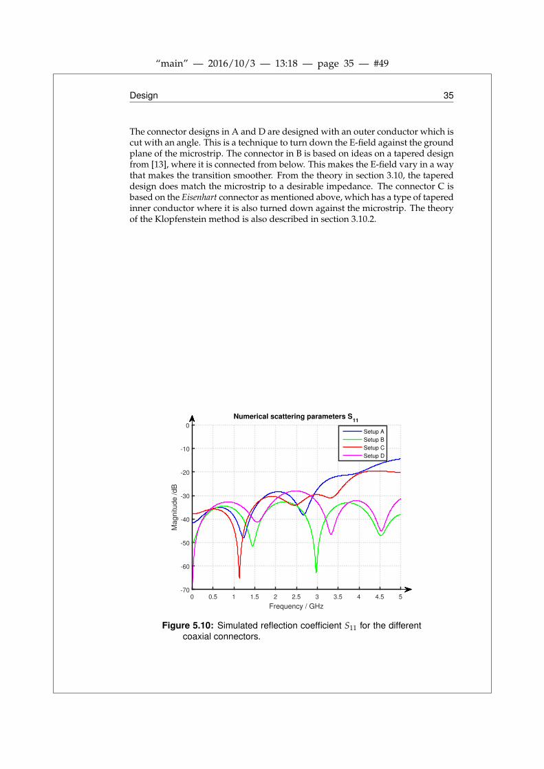
The transition is investigated and simulated and the result is shown in Fig. 5.8.It can be seen from the figure how the E-field varies from the coaxial line to themicrostrip line. The coaxial line contains teflon and the microstrip contains airin the guiding direction. The coaxial part is tapered to smooth the transitionand to compensate for the discontinuities and reflections. Referring to section4.1 and identifying the correct scattering parameter, which for this case is the re-flection parameter S11, is a measure of how well matched the transitions can bemade. Different setups were simulated by numerically determination which kindof transition will offer the best solution that matches the specification. The Eisen-hart connector and the reasoning around the mentioned connector [36] togetherwith transition techniques from [37, 38] are used as a source of inspiration whiledesigning the connector with respect to smooth transition with low reflection.The technique used is a tapered part in the connector to get a smooth transitionfor the E-field while designing a connector from underneath. Fig. 5.9 shows fourdifferent kinds of connectors. The reflection and transmission parameter are plot-ted in Fig. 5.10 and Fig. 5.11. Fig. 5.10 shows the reflection parameter for fourdifferent types of coaxial to microstrip connectors.The complexity of the match-ing is increasing because of the operating bandwidth requirement given in thespecifications.
Figure 5.9: Design of Coaxial connectors A-D.
“main” — 2016/10/3 — 13:18 — page 35 — #49
Design 35
The connector designs in A and D are designed with an outer conductor which iscut with an angle. This is a technique to turn down the E-field against the groundplane of the microstrip. The connector in B is based on ideas on a tapered designfrom [13], where it is connected from below. This makes the E-field vary in a waythat makes the transition smoother. From the theory in section 3.10, the tapereddesign does match the microstrip to a desirable impedance. The connector C isbased on the Eisenhart connector as mentioned above, which has a type of taperedinner conductor where it is also turned down against the microstrip. The theoryof the Klopfenstein method is also described in section 3.10.2.
0 0.5 1 1.5 2 2.5 3 3.5 4 4.5 5
Frequency / GHz
-70
-60
-50
-40
-30
-20
-10
0
Magnitude /dB
Numerical scattering parameters S11
Setup A
Setup B
Setup C
Setup D
Figure 5.10: Simulated reflection coefficient S11 for the differentcoaxial connectors.

“main” — 2016/10/3 — 13:18 — page 36 — #50
36 Design
0 0.5 1 1.5 2 2.5 3 3.5 4 4.5 5
Frequency / GHz
-1
-0.9
-0.8
-0.7
-0.6
-0.5
-0.4
-0.3
-0.2
-0.1
0M
agnitude /dB
Numerical scattering parameters S21
Setup A
Setup B
Setup C
Setup D
Figure 5.11: Simulated transmission coefficient S21 for the differ-ent coaxial connectors.
By examining the scattering parameters further, one can see that both the reflec-tion S11 and transmission parameters, S21 in Fig. 5.10 and Fig. 5.11 respectively,have a slight correlation. For example the green line (setup B) have the best trans-mission parameters because it’s reflection parameters is the lowest over the mea-sured frequency range. The important part is to examine how the two differ-ent parameters affect the calculation of the electric permittivity and permeability.This is done by multiple simulations with a given material which for this case isteflon. Because of the complexity of the problem one needs to vary a number ofvariables and compare the result relative to the expected output. Connector in Boffers low reflection over the whole spectrum and has the best transmission, thusthis connector is chosen to be manufactured for the TEM cell.
5.4 Tapered microstrip linesThe excitation platform is matched to the coaxial cable and its dimension is therebylimited by the coaxial cable. Referring to the design specification of the waveg-uide, sample that are of manageable size concerning manufacturing of differentkind of test material is the main aspect. This requires a transition from the smallmicrostrip to a larger microstrip, inspired from Klopfenstein which is discussedin section 3.10.2. The microstrip was simulated in CST and dimensions of themicrostrip was based on ideas from [39, 40], where an optimum tapered trans-mission line is analyzed. Ideas were also taken from [34], where an improveddesign with Klopfenstein tapering was investigated. Every little section of the ta-pering can be seen as a small microstrip. It is important to preserve the matching

“main” — 2016/10/3 — 13:18 — page 37 — #51
Design 37
and minimize the losses when the tapering is designed. Smooth transitions areimportant to minimize the risk of triggering higher order modes from propagat-ing in the waveguide and interference with the desired TEM mode.
Figure 5.12: Tapered microstrip lines in highlighted shape.
5.5 Planar section of the TEM cellThe planar section shown in Fig. 5.13 can be seen as a larger microstrip, referringto the microstrip line in section 5.1, where the impedance is matched to 50Ω. Thesize of the planar section is determined from the size of the test sample and thescattering parameters, and is limited of when the higher order modes can start topropagate. According to Eq. (3.31) the first higher order mode can start to prop-agate at around 2.6Ghz. This mode may start to propagate later as it is affectedby the physical geometry of the TEM cell, for example by the tapered microstriplines and the refined surface to eliminate discontinuities in the material. Thiscounteract the higher order modes to be triggered. The simulation of the struc-ture in CST and then optimizing it for the best matching to satisfy the calculationof the material parameters is the most important aspect when preventing this.
Figure 5.13: The planar section, in highlighted shape, coveringthe test sample.
“main” — 2016/10/3 — 13:18 — page 38 — #52
38 Design
5.6 Test sample
Figure 5.14: The test sample in highlighted shape.
The test sample is placed in between the ground plane and the planar section ascan be seen in Fig. 5.14. When the first version of the waveguide fixture is de-signed, an attempt is made to characterize the material parameters of teflon inthe CST simulation environment. Teflon is known to be a stable material withpermittivity ε = 2.1 for a wide range of frequencies and it serves as a good firstexperimental test. The Baker Jarvis and Nicolson-Ross-Weir algorithm from sec-tion 2.4 is modified to match the given fixture and the permittivity and perme-ability is calculated from the scattering parameters. To calculate the permittivityin the Baker Jarvis algorithm, a calibration with the empty line is done and thefield pattern is shown in Fig. 5.15.
Figure 5.15: Simulated E-field in dB scale of the TEM cell withoutthe test sample.
The E-field is bound to the fixture under the conducting plate and there is alsofringing fields. The fringing fields depend on the medium where the electromag-netic waves are propagating. Higher permittivity of the surrounding dielectricmaterial binds the field which in turn result in less fringing fields [31]. To normal-ize the scattering parameter, an empty line was simulated and then simulation is

“main” — 2016/10/3 — 13:18 — page 39 — #53
Design 39
done to the actual test piece in the waveguide. The normalization or calibrationis done when dividing the two scattering parameters to eliminate losses whichdoes not occur from the actual test sample. Different widths are simulated, whilethe thickness and height is the same, to analyze how the E-field varies.
Figure 5.16: Simulated E-field in dB scale with Teflon as testsample. Width of test sample 150mm.
Fig. 5.16 shows the E-fields for a test sample which cover the whole conductingplane and the size of the ground plane. The experiment is made to measure howdifferent widths affect the final value of the calculated permittivity and to studythe phenomena of fringing fields and leakage.
Figure 5.17: Simulated E-field in dB scale of Teflon as test sam-ple. Width of test sample 100mm.

“main” — 2016/10/3 — 13:18 — page 40 — #54
40 Design
Figure 5.18: Simulated E-field in dB scale of Teflon as test sam-ple. Width of test sample 56mm.
Fig. 5.17 and Fig. 5.18 show simulated E-fields of different widths of the test sam-ple. The E-field pattern does not reveal the whole truth. There is a difference inthe electric field distribution due to the different widths but a graph with the dif-ferent calculated parameters reveals how the result is affected and which width ispreferred when doing the measurement. Fig. 5.19 shows the four different casesinvestigated.
0 0.5 1 1.5 2 2.5 3 3.5 4 4.5 5
Frequency / GHz
0.8
1
1.2
1.4
1.6
1.8
2
Perm
ittivity
Numerical Permittivity of Teflon (loss free)
Sample 150mm
Sample 100mm
Sample 56mm
Empty
Figure 5.19: Simulated Permittivity for teflon as test sample fordifferent widths.
Referring to Fig 5.19 there is a significant difference between the size and thepermittivity. Ideal permittivity for the simulated air is εr = 1. The smallest testsample has a bigger error due to the leakage of the E-field. To minimize the error,the test sample with width of 150mm is chosen.

“main” — 2016/10/3 — 13:18 — page 41 — #55
Design 41
5.7 Ground plane
Figure 5.20: Ground plane of the fixture in highlighted shape.
The size of the ground plane affect both the transmission and the reflection pa-rameter. Different widths of the ground plane was simulated in CST and thescattering parameters was studied. The ground plane is selected to be as small aspossible without interfering with the measurement accuracy.
5.8 Stabilizer
Figure 5.21: Plastic frame with bolts to stabilize and adjust thefixture, in highlighted shape.
The choice to use a plastic frame supporting structure shown in Fig. 5.21 is be-cause of the fixture length and to be able to tighten the test sample so no leakageoccurs between the planar section and the ground plane. Another reason is to beable to adjust the width to height ratio matching when connected to the networkanalyzer. The bolts are mounted to the top of the tapered microstrip and can eas-ily be adjusted by the screws. The stabilizing frame which includes the bolts is

“main” — 2016/10/3 — 13:18 — page 42 — #56
42 Design
constructed in Delrin (Acetal Resin) which is an electrically insulating and rigidmaterial. The choice of location and dimension of the stabilizer is to make surethat the influence to the E-field is as low as possible.
Figure 5.22: Bolts mounted on top of the structure to adjust thewidth to height ratio.
5.9 Final Simulated Design
Waveguides can be designed in many ways and a number of variables need tobe taken into account. When a first layout is designed and the desired resultis achieved the waveguide needs to be tested. A table with different data forsimulated structures are shown in Fig 5.1.
Table 5.1: Table of dimensions (in mm) of the different setupsA-D.
Setup A Setup B Setup C Setup DGround plane 500x150x6 500x150x6 533x150x6 596x150x6Planar section 40.5x27x3 56x32.2x3 40.5x40x3 45x30x3Test sample 100x29x9 100x32.2x12 100x30x8 100x30x10
The scattering parameters are simulated in CST. Fig. 5.23 shows the differentreflection parameters of the different setups.

“main” — 2016/10/3 — 13:18 — page 43 — #57
Design 43
0 0.5 1 1.5 2 2.5 3 3.5 4 4.5 5
Frequency / GHz
-70
-60
-50
-40
-30
-20
-10
0
Magnitude /dB
Numerical scattering parameters S11
Setup A
Setup B
Setup C
Setup D
Figure 5.23: Simulated reflection coefficient S11 the different se-tups.
Fig. 5.24 shows the transmission coefficients for the setups in the table.
0 0.5 1 1.5 2 2.5 3 3.5 4 4.5 5
Frequency / GHz
-2
-1.5
-1
-0.5
0
Magnitude /dB
Numerical scattering parameters S21
Setup A
Setup B
Setup C
Setup D
Figure 5.24: Simulated transmission coefficient S21of the differ-ent setups.
Having the data plotted one can compare the different setups with each other,

“main” — 2016/10/3 — 13:18 — page 44 — #58
44 Design
but to achieve relevant results, different materials needs to be measured in thedifferent setups to determine which parameters are most significant for the finaldesign. By setting up a numerical experiment in CST and exporting the scatter-ing parameters, the permittivity and permeability can be determined from theNicolson-Ross-Weir Eq. (2.11) and Baker Jarvis Eq. (2.13) algorithm. In the fol-lowing figures there are a range of simulated materials in the different setups.The size and shape of the test sample are the same for all materials, it is only thetype of material and setup that varies. The test is performed in such a way that adecision on which design is most appropriate for the task can be selected.
0 0.5 1 1.5 2 2.5 3 3.5 4 4.5 5
Frequency / GHz
1.5
1.55
1.6
1.65
1.7
1.75
1.8
1.85
1.9
1.95
2
Perm
ittivity
Numerical Permittivity of Teflon (loss free)
Setup A
Setup B
Setup C
Setup D
Figure 5.25: Permittivity of Teflon with Baker Jarvis algorithm ofthe different setups using simulated data.

“main” — 2016/10/3 — 13:18 — page 45 — #59
Design 45
0 0.5 1 1.5 2 2.5 3 3.5 4 4.5 5
Frequency / GHz
2
2.1
2.2
2.3
2.4
2.5
2.6
2.7
2.8
Perm
ittivity
Numerical Permittivity of Rubber (loss free)
Setup A
Setup B
Setup C
Setup D
Figure 5.26: Permittivity of Rubber with Baker Jarvis algorithmof the different setups using simulated data.
0 0.5 1 1.5 2 2.5 3 3.5 4 4.5 5
Frequency / GHz
2.5
3
3.5
4
Perm
ittivity
Numerical Permittivity of Epoxy Resin (loss free)
Setup A
Setup B
Setup C
Setup D
Figure 5.27: Permittivity of Epoxy Resin with Baker Jarvis algo-rithm of the different setups using simulated data.

“main” — 2016/10/3 — 13:18 — page 46 — #60
46 Design
0 0.5 1 1.5 2 2.5 3 3.5 4 4.5 5
Frequency / GHz
4
4.5
5
5.5
6
6.5P
erm
ittivity
Numerical Permittivity of Lead Glass (loss free)
Setup A
Setup B
Setup C
Setup D
Figure 5.28: Permittivity of Lead glass with Baker Jarvis algo-rithm of the different setups using simulated data.
Comparing the results in the above Fig. 5.25-5.28 with the simulated permittiv-ity for different kinds of materials one can predict which setup is best for thispurpose based on the given specification. The setup in B offers smoother plotsof the measured permittivity and has the lowest S11 parameter over the spec-trum, shown in Fig. 5.23. As can be seen in Fig. 5.24, this offers a slightly lowertransmission coefficient S21. To maximize the accuracy of the relevant result thewaveguide with the best reflection parameter, setup B is chosen to be manufac-tured.

“main” — 2016/10/3 — 13:18 — page 47 — #61
Design 47
0 0.5 1 1.5 2 2.5 3 3.5 4 4.5 5
Frequency / GHz
-70
-60
-50
-40
-30
-20
-10
0
Magnitude /dB
Numerical scattering parameters
S11
S21
S22
S12
Figure 5.29: Simulated transmission and reflection of the finaldesign (Setup B).
Fig 5.29 shows the scattering parameters for the chosen setup. One can see howthe reflection coefficient S11 varies over the simulated frequency range. The S21parameter shows the transmission coefficient. The result of the numerical simu-lation satisfies the expectations on an open waveguide considering interferencefrom ambient and leakage due to the advanced design.

“main” — 2016/10/3 — 13:18 — page 48 — #62
48 Design

“main” — 2016/10/3 — 13:18 — page 49 — #63
Chapter6Manufacturing
6.1 Initial test designBefore manufacturing the actual measuring setup, a test design was made on amicrostrip to get an idea of the stability of the material. The transition from anSMA-connector that was soldered onto it was investigated and verification of thetheoretically calculated characteristic impedance was made. Brass was used asmaterial for the test setup and was manufactured at Saab. The SMA-connectorswere mounted from underneath the ground plane, where the inner conductor ofthe connector was soldered to the microstrip, as shown in Fig. 6.1. The resultingvalues showed good transmission and reflections of -20dB over the frequency 0-5GHz while using the network analyzer. By tilting the microstrip, this gave anidea of how much impact the width to height ratio has for the microstrip in senseof the characteristic impedance, as described in section 3.4.
Figure 6.1: Manufactured test design with coaxial SMA-connectors.
6.2 MaterialsThe material selected for the measurement setup is aluminum because of its highelectrical conductivity and rigid properties. The measurement setup needs to beperfectly matched to the model in CST with respect to straight conducting platesand refined surfaces, to avoid discontinuities in the electromagnetic field. The
49

“main” — 2016/10/3 — 13:18 — page 50 — #64
50 Manufacturing
measuring setup must also be mechanically stable to handle movements whileusing or moving the setup. This is mostly managed by the stabilizer that is alsoused to adjust the setup, as mentioned in section 5.8. The stabilizer frame includ-ing bolts is manufactured in Delrin (Acetal Resin), which is a good isolating andrigid material, as described in section 5.8.
6.3 Connector
Figure 6.2: Standard female N-connector.
The coaxial connector is a standard female N-connector, Fig. 6.2, that is mountedfrom the bottom of the ground plane. It is a large size connector and was choseninstead of the SMA-connector, that was first used on the test design, because ofits more rigid structure with a larger inner conductor. The inner conductor of theconnector is connected to the microstrip with a cone-shaped structure. The cone-shaped part is first mounted to the connector by "conducting glue", which createsa good electromagnetic transition between the two parts. The connector is thenpermanently threaded into the microstrip which creates a mechanical stable andhighly conducting transition, shown in Fig. 6.3.
Figure 6.3: Manufactured pieces for the transition between thecoaxial connector and microstrip.

“main” — 2016/10/3 — 13:18 — page 51 — #65
Manufacturing 51
6.4 Test sample
The test samples used for the measurements in this project are manufactured inteflon, bakelite and an unknown material and are of size 150x32x12mm3. Themanufacturing of accurate test sample sample can be a complicated task. Themilling machine was used to manufacture the test sample, since the measure-ment is influenced by how accurate the sample can be made. In this case, thesurface smoothness is significant and must be essentially perfect to prevent fieldleakage as described in section 5.6. The teflon material was the most difficult partto process. It is a soft material that would melt if milled to fast. Therefore thematerial was processed with the milling machine at slow pace and crystal oil wasused to prevent the material from overheating and meltdown. The same proce-dure was used for the bakelite and the unknown material to get as good qualitytest samples as possible. Fig. 6.4 below shows the test samples that were manu-factured.
Figure 6.4: Manufactured test samples in an unknown material,teflon material and bakelite material.

“main” — 2016/10/3 — 13:18 — page 52 — #66
52 Manufacturing
6.5 Final design
The measuring setup is manufactured at Saab Aerostructures manufacturing En-gineering department. Most of it was made by ourselves with sandpaper, raspand polisher, with professional assistance while handling the milling machines,Fig. 6.5.
Figure 6.5: Saab Aerostructures manufacturing EngineeringShort Series Production and Spares department. A testsample in bakelite is currently being manufactured in themilling machine to the left. The authors are also present inthe picture.
The final manufactured design is shown in Figs. 6.6-6.9. The material used is Alu-minum as described in section 6.1 and the surface of the structure is processed toget a refined finish. This is done to get rid of any discontinuities in the mate-rial to prevent noise and distortion of the signal. The material is first processedwith sandpaper, and is then further on processed with a sander. Autosol R©MetalPolish was then used to get the glossy refined finish.

“main” — 2016/10/3 — 13:18 — page 53 — #67
Manufacturing 53
Figure 6.6: Manufactured final design with an inserted test sam-ple.
Figure 6.7: Manufactured final design viewed from above.

“main” — 2016/10/3 — 13:18 — page 54 — #68
54 Manufacturing
Figure 6.8: Manufactured final design viewed from one of thecoaxial connectors.
Figure 6.9: Manufactured final design with close up view of thetransition from one of the coaxial connectors.

“main” — 2016/10/3 — 13:18 — page 55 — #69
Chapter7
Validation and Verification
Validation and verification of the manufactured TEM cell is performed usingmeasurements of three different material samples. The three materials are teflon,bakelite and a material with unknown permittivity. Teflon and bakelite are cho-sen, because of the relatively well-known permittivity over the frequency range 0-5GHz. One important aspect of the material selection is to be able to compare thereal measurements with the simulated measurements in the CST environment.By collecting data from the numerical simulations and the actual measurement,different conclusions about the finished prototype can be made. To be able to usethe Baker Jarvis Eq. (2.13) algorithm one needs to know the scattering parametersof an empty TEM cell. Scattering parameters are also used to measure how wellthe TEM cell works and to give a hint of how precise the measurements can bedone with the TEM cell. Fig 7.1 shows the scattering parameters for the emptyTEM cell.
55

“main” — 2016/10/3 — 13:18 — page 56 — #70
56 Validation and Verification
0 0.5 1 1.5 2 2.5 3 3.5 4 4.5 5
Frequency / GHz
-70
-60
-50
-40
-30
-20
-10
0M
agnitude /dB
Measured scattering parameters
S11
S21
S22
S12
Figure 7.1: Measured scattering parameters of the empty TEMcell.
We also provide the reader with the numerical simulated scattering parametersfor the empty TEM cell, in Fig. 7.2, for comparison.
0 0.5 1 1.5 2 2.5 3 3.5 4 4.5 5
Frequency / GHz
-70
-60
-50
-40
-30
-20
-10
0
Magnitude /dB
Numerical scattering parameters
S11
S21
S22
S12
Figure 7.2: Numerical scattering parameters of the empty TEMcell.

“main” — 2016/10/3 — 13:18 — page 57 — #71
Validation and Verification 57
Comparing Fig. 7.1 and Fig. 7.2 one can realize that the reflection parameters S11and S22 are not the same. The numerical reflection parameters overlap becausethe two ports are identical with each other which generates the same impedance.For the case with the real setup the ports are hard to manufacture as two identi-cal pairs and some errors may occur from the differences, which is shown in Fig.7.1. While comparing the measured S11 and S22, with the simulated values, onecan see that there is a noticeable difference. The simulated values are significantlower over the whole spectrum. This may be because of the fact that the realsetup is not perfectly manufactured. There are several transitions which causesdiscontinuities in the real setup, which in turn affects the reflection coefficient.Transmission coefficient follow each other well. This means that the numericaldata is consistent with the measured data.
To verify the results of the TEM cell, a test is done with an empty TEM cell. Byknowing that the relative permittivity of air is εr = 1 and the distance betweenthe two excitation ports is 486mm, one can calculate the permittivity of the emptyTEM cell with Baker Jarvis algorithm. The result is shown in Fig. 7.3.
0 0.5 1 1.5 2 2.5 3 3.5 4 4.5 5
Frequency / GHz
-0.2
0
0.2
0.4
0.6
0.8
1
1.2
Perm
ittivity
Measured Complex Permittivity of Air
Air (real part)
Air (imaginary part)
Figure 7.3: Measured permittivity of air.
The real part of the complex permittivity of air is εr = 1 over the measured fre-quency interval. The imaginary part are a measure of the losses in the materialand for air there are no measurable losses.
To test the algorithm and verify that the measured data is correct, a known caseis used. Air has almost the same permittivity as vacuum which is εr = 1. The realpermittivity is one over the measured frequency range and there are no losseswhich can be seen from the imaginary part of the plot.

“main” — 2016/10/3 — 13:18 — page 58 — #72
58 Validation and Verification
Teflon is a reliable test sample due to its known characteristics. A test sampleof teflon was milled with the size 150x32x12mm3. Fig. 7.4 shows the measuredvalue of teflon with the TEM cell.
0 0.5 1 1.5 2 2.5 3 3.5 4 4.5 5
Frequency / GHz
-0.5
0
0.5
1
1.5
2
Perm
ittivity
Measured Complex Permittivity of Teflon
Teflon (real part)
Teflon (imaginary part)
Figure 7.4: Measured permittivity of teflon.
To verify the real measurement a graph with the numerical simulated values ofteflon are shown in Fig. 7.5.
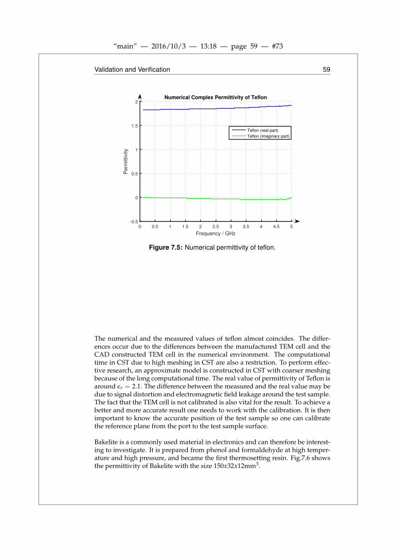
“main” — 2016/10/3 — 13:18 — page 59 — #73
Validation and Verification 59
0 0.5 1 1.5 2 2.5 3 3.5 4 4.5 5
Frequency / GHz
-0.5
0
0.5
1
1.5
2
Perm
ittivity
Numerical Complex Permittivity of Teflon
Teflon (real part)
Teflon (imaginary part)
Figure 7.5: Numerical permittivity of teflon.
The numerical and the measured values of teflon almost coincides. The differ-ences occur due to the differences between the manufactured TEM cell and theCAD constructed TEM cell in the numerical environment. The computationaltime in CST due to high meshing in CST are also a restriction. To perform effec-tive research, an approximate model is constructed in CST with coarser meshingbecause of the long computational time. The real value of permittivity of Teflon isaround εr = 2.1. The difference between the measured and the real value may bedue to signal distortion and electromagnetic field leakage around the test sample.The fact that the TEM cell is not calibrated is also vital for the result. To achieve abetter and more accurate result one needs to work with the calibration. It is thenimportant to know the accurate position of the test sample so one can calibratethe reference plane from the port to the test sample surface.
Bakelite is a commonly used material in electronics and can therefore be interest-ing to investigate. It is prepared from phenol and formaldehyde at high temper-ature and high pressure, and became the first thermosetting resin. Fig.7.6 showsthe permittivity of Bakelite with the size 150x32x12mm3.

“main” — 2016/10/3 — 13:18 — page 60 — #74
60 Validation and Verification
0 0.5 1 1.5 2 2.5 3 3.5 4 4.5 5
Frequency / GHz
-0.5
0
0.5
1
1.5
2
2.5
3P
erm
ittivity
Measured Complex Permittivity of Bakelite
Bakelite (real part)
Bakelite (imaginary part)
Figure 7.6: Measured permittivity of bakelite.
Fig. 7.7 shows the simulated values of bakelite.
0 0.5 1 1.5 2 2.5 3 3.5 4 4.5 5
Frequency / GHz
0
0.5
1
1.5
2
2.5
3
3.5
4
4.5
Perm
ittivity
Numerical Complex Permittivity of Bakelite
Bakelite (real part)
Bakelite (imaginary part)
Figure 7.7: Numerical permittivity of bakelite.
Studying the two different graphs of bakelite shows that the values does notcoincides. Bakelite is not a well-defined material compared with teflon, and in
“main” — 2016/10/3 — 13:18 — page 61 — #75
Validation and Verification 61
pitched tables sets, bakelite permittivity varies between 3.5-5, which depends onthe test sample recipe and manufacturing process. The measured value may alsobe slightly lower than the real value, caused by the signal distortion and electro-magnetic field leakage as for the measured Teflon.
When the TEM cell is tested and verified, a test with an unknown material wasmade. From the plot, a guess can be made on which material the test sampleconsists of when looking at known tables from example [41]. Fig. 7.8 shows theresult.
0 0.5 1 1.5 2 2.5 3 3.5 4 4.5 5
Frequency / GHz
0
0.5
1
1.5
2
2.5
3
Perm
ittivity
Measured Complex Permittivity of Unknown sample
Unknown sample (real part)
Unknown sample (imaginary part)
Figure 7.8: Measured permittivity of an Unknown material.
The measured data seems to be relatively smooth over the measured frequencyrange. Fig. 7.8 indicates that the relative permittivity, εr ≈ 2.6. From the tablesand a quick analyze of the material an educated guess can be made resulting insome kind of resin material. Resin is made of different kinds of material wherethe recipe varies. The mixture of different materials can lead to the permittivityvariations given at tabulated data.
7.1 Operating bandwidth test of the TEM cellAfter the validation and verification of the results presented in the section above,an operating bandwidth test was made for the TEM cell. As can be seen in Fig.7.9, the network analyzer was set to 0-10GHz, which shows the scattering param-eters.

“main” — 2016/10/3 — 13:18 — page 62 — #76
62 Validation and Verification
0 1 2 3 4 5 6 7 8 9 10
Frequency / GHz
-70
-60
-50
-40
-30
-20
-10
0M
agnitude /dB
Measured scattering parameters
S11
S21
S22
S12
Figure 7.9: Measured scattering parameters of the empty TEMcell.
The numerical values of the S-parameters is presented in Fig. 7.10. It can be seenthat the transmission parameters, S12 and S21 is less damped than the reflectioncoefficients S11 and S22.

“main” — 2016/10/3 — 13:18 — page 63 — #77
Validation and Verification 63
0 1 2 3 4 5 6 7 8 9 10
Frequency / GHz
-70
-60
-50
-40
-30
-20
-10
0
Magnitude /dB
Numerical scattering parameters
S11
S21
S22
S12
Figure 7.10: Numerical scattering parameters of the empty TEMcell.
Analyzing the measured scattering parameters of an empty TEM cell for a widerfrequency spectrum gives an interesting result. The transmission coefficient in-tersects the reflection coefficient at somewhere around 9GHz. This will lead to anerror where the TEM cell and the Baker Jarvis algorithm would not work prop-erly over 9GHz. By studying the numerical values of the S-parameters for theempty TEM cell, this gives an indication that the TEM cell may work for higherfrequencies. As described before, the transmission and reflection coefficient islimited to how accurate the measuring setup can be manufactured, which sets anlimit of how well it can perform. The TEM cell works for frequencies higher than5GHz which means that the TEM cell outperforms the given design specification.
The bandwidth test is performed with an empty TEM cell. The data of air ismeasured and then calculated with Baker Jarvis. Fig. 7.11 shows the permittivityof air for the wider bandwidth test.

“main” — 2016/10/3 — 13:18 — page 64 — #78
64 Validation and Verification
0 1 2 3 4 5 6 7 8 9 10
Frequency / GHz
-0.2
0
0.2
0.4
0.6
0.8
1
1.2P
erm
ittivity
Measured Complex Permittivity of Air
Air (real part)
Air (imaginary part)
Figure 7.11: Measured permittivity of Air.
From Fig. 7.11 one can see that the TEM cell performs well up to the intersectionpoint 9Ghz. The algorithm gets unstable when the intersection occurs where thedata from 9-10GHz is not reliable.
A last bandwidth test is made with teflon. Two different figures represent thein-data of the algorithm, Fig. 7.12, and the processed data is shown in Fig. 7.13
“main” — 2016/10/3 — 13:18 — page 65 — #79
Validation and Verification 65
0 1 2 3 4 5 6 7 8 9 10
Frequency / GHz
-70
-60
-50
-40
-30
-20
-10
0
Magnitude /dB
Measured scattering parameters
S11
S21
S22
S12
Figure 7.12: Measured scattering parameters of Teflon.
0 1 2 3 4 5 6 7 8 9 10
Frequency / GHz
0
1
2
3
4
5
6
7
8
9
10
Perm
ittivity
Measured Complex Permittivity of Teflon
Teflon (real part)
Teflon (imaginary part)
Figure 7.13: Measured permittivity of Teflon.
Analyzing Fig. 7.12 and Fig. 7.13 gives a clear connection between the BakerJarvis algorithm and the S-parameters at ∼9GHz. The TEM cell performs wellup to 9GHz for teflon and gives an upper limit of when reliable values exists.To understand what happens at 9GHz, one needs to dive deeper into the Baker

“main” — 2016/10/3 — 13:18 — page 66 — #80
66 Validation and Verification
Jarvis algorithm (2.13) and analyze how the S-parameters is derived and affectsthe algorithm, which is not further discussed in this thesis.
After the TEM cell was designed and manufactured one major question rose,namely which is the best calibration method for the new type of TEM cell? Thereare a lot of calibration methods for today’s waveguide, but neither of them wereparticularity developed for the new design. In the development stage of the newmodel one can explore new calibration methods, a method which is of particularinterest is discussed in [8]. The method changes the S-matrix from the calibrationreference plane to the test sample reference plane, with an optimization algo-rithm and then theoretically calculates the complex permittivity and permeabil-ity. There is also an interesting algorithm [42] that combines Nicolson-Ross-Weirand the Baker Jarvis algorithm which can be used to improve the measuring re-sult.
The final and the numerically simulated TEM cell can be improved with a bettercalibration technique as mentioned above and with a refined manufacturing pro-cess. Trying to manufacture two identical ports can improve both the reflectionand the transmission parameters, which will lead to higher operating bandwidthfor the TEM Cell. The measurement results for the given test samples achievedabove has a consequent deviation of the permittivity from the real value. If anoptimal calibration method was found, the TEM cell could be used to measurecomplex permittivity for the frequency range 0-8GHz for low permittivity mate-rials.

“main” — 2016/10/3 — 13:18 — page 67 — #81
Chapter8Conclusions
There are a lot of aspects that needs to be taken into account while designing thistype of waveguide. An open waveguide fixture causes field leakages and refinedmanufacturing processes of the edges and the surfaces becomes vital for the re-sulting measurements. Manufacturing a TEM cell of this type requires precisionand the geometry of the TEM cell needs to follow the simulated dimensions toget a good matching for the S-parameters. The transition from the coaxial cableto the TEM cell was challenging and considerations in the design part needs tobe taken into account to be able to manufacture it. In practice the two ports needto be symmetric to get the same transmission and reflection coefficients of bothsides, which is difficult to achieve. The manufacturing of the test sample is im-portant for the accuracy of the measurement and a refined process is crucial toavoid electromagnetic field leakage between the test sample and the conductingplates of the TEM cell.
CST is a numerical computational program which was used in the designing part.The simulation part is necessary while testing new designs of the TEM cell andrestrictions in computational power slows down the process. To speed up thedesign process, a custom computational computer specifically built for the sim-ulation program is highly recommended. The numerical program gives a goodhint of the real world and is relatively accurate if handled properly.
The TEM cell works well and with a little more development one can refine themeasurements. The electromagnetic field leakage due to the open TEM cell de-sign gives a relatively consistent error in the measurement. After analyzing thethree different types of test samples that were used in the measurements, the er-ror can be quantified to 14%. This error can be further investigated to increasethe accuracy of the TEM cell. Processing the collected data and filtering it fromsignals that is leaking around the test sample may increase the accuracy for themeasurements. The filtering process can be obtained with for example FourierTransforms, where the difference in phase shift can be used to decide which sig-nals to be eliminated. Without using a filtering process, and instead consideringa compensation factor of 1.14 for the leakage, the TEM cell results in an accuracywithin one tenth of a decimal point for the given test sample materials.
67

“main” — 2016/10/3 — 13:18 — page 68 — #82
68 Conclusions
The operating bandwidth of the TEM cell was higher than expected. To avoidthe higher order modes from propagating, it is important that the surfaces of theconductive plates is as smooth as possible to prevent discontinuities which is trig-gering the higher order modes. We are not aware of any similar TEM cell designmade with microstrip theory and that was challenging. Now the ball is rollingand a first edition of a TEM cell, inspired by a microstrip, is manufactured. Let’ssee how accurate this design can become in the future.

“main” — 2016/10/3 — 13:18 — page 69 — #83
References
[1] K. L. Shlager, G. S. Smith, and J. G. Maloney. Accurate analysis of tem hornantennas for pulse radiation. IEEE Transactions on Electromagnetic Compati-bility, 38(3):414–423, Aug 1996. ISSN 0018-9375. doi: 10.1109/15.536071.
[2] J. C. Tippet and D. C. Chang. Radiation characteristics of electricallysmall devices in a tem transmission cell. IEEE Transactions on Electromag-netic Compatibility, EMC-18(4):134–140, Nov 1976. ISSN 0018-9375. doi:10.1109/TEMC.1976.303492.
[3] T. Mandic, R. Gillon, B. Nauwelaers, and A. Baric. Characterizing the temcell electric and magnetic field coupling to pcb transmission lines. IEEETransactions on Electromagnetic Compatibility, 54(5):976–985, Oct 2012. ISSN0018-9375. doi: 10.1109/TEMC.2012.2193888.
[4] K. Malaric and I. Bacic. Efficiency of the materials used in building tem-cell.In Microwave Techniques, 2008. COMITE 2008. 14th Conference on, pages 1–3,April 2008. doi: 10.1109/COMITE.2008.4569957.
[5] Sandeep M. Satav and Vivek Agarwal. Do-it-yourself fabrication of an opentem cell for emc pre-compliance. EMI-EMC Center RCI and Dept. of ElectricalEngineering, Indian Institute of Technology-Bombay, 2008.
[6] C. Iftode, S. Miclaus, P. Bechet, and E. Surducan. A tem cell model analy-sis for radiofrequency dosimetry improvement by computational means. InAdvanced Topics in Electrical Engineering (ATEE), 2011 7th International Sym-posium on, pages 1–4, May 2011.
[7] M. Borsero, G. Vizio, D. Parena, and V. Teppati. Synthetic tdr measure-ments for tem and gtem cell characterization. IEEE Transactions on Instru-mentation and Measurement, 56(2):271–274, April 2007. ISSN 0018-9456. doi:10.1109/TIM.2007.890796.
[8] R. Tumayan, X. Bunlon, A. Reineix, G. Andrieu, and C. Guiffaut. A methodusing an open tem cell to extract the complex permittivity of an unknownmaterial. In 2014 International Symposium on Electromagnetic Compatibility,pages 1102–1106, Sept 2014. doi: 10.1109/EMCEurope.2014.6931067.
69

“main” — 2016/10/3 — 13:18 — page 70 — #84
70 REFERENCES
[9] S. J. Orfanidis. Electromagnetic Waves and Antennas.www.ece.rutgers.edu/ orfanidi/ewa, 1999-2014.
[10] M. Yarleque and A. Miranda. Permittivity measuring technique based ona parallel-plate waveguide concept. In Andean Region International Con-ference (ANDESCON), 2012 VI, pages 67–70, Nov 2012. doi: 10.1109/An-descon.2012.25.
[11] A. Kazemipour, D. Allal, A. Litwin, and M. Bourghes. Wideband temparallel-plate cell for sar-probe calibration. In CPEM 2010, pages 710–711,June 2010. doi: 10.1109/CPEM.2010.5543503.
[12] Standard test method for measuring relative complex permittivity and rela-tive magnetic permeability of solid materials at microwave frequencies us-ing waveguide. ASTM International, 10.02, 2008. doi: 10.1520/D5568-14.
[13] S. K. Yee, A. Sayegh, A. Kazemipour, and M. Z. M. Jenu. Design and calibra-tion of a wideband tem-cell for material characterization. In 2012 Asia-PacificSymposium on Electromagnetic Compatibility, pages 749–752, May 2012. doi:10.1109/APEMC.2012.6237852.
[14] S. Hilavin and A. Kustepeli. Design and implementation of a tem striplinefor emc testing. IEEE Transactions on Electromagnetic Compatibility, 56(1):23–27, Feb 2014. ISSN 0018-9375. doi: 10.1109/TEMC.2013.2271834.
[15] M. L. Crawford. Generation of standard em fields using tem transmissioncells. IEEE Transactions on Electromagnetic Compatibility, EMC-16(4):189–195,Nov 1974. ISSN 0018-9375. doi: 10.1109/TEMC.1974.303364.
[16] P. F. Wilson and M. T. Ma. Simple approximate expressions for higher or-der mode cutoff and resonant frequencies in tem cells. IEEE Transactions onElectromagnetic Compatibility, 28(3):125–130, Aug 1986. ISSN 0018-9375. doi:10.1109/TEMC.1986.4307269.
[17] C. Rostamzadeh, B. Archambeault, and S. Connor. Fdtd analysis of sym-metric tem cell. In 2005 International Symposium on Electromagnetic Compat-ibility, 2005. EMC 2005., volume 2, pages 525–529 Vol. 2, Aug 2005. doi:10.1109/ISEMC.2005.1513571.
[18] John H. Grosvenor Jr. Richard G.Geyer James Baker-Jarvis, MichaelD. Janezic. Transmission/Reflection and Short-Circuit Line Methods for Measur-ing Permittivity and Permeability. NIST, 1992.
[19] A. M. Nicolson and G. F. Ross. Measurement of the intrinsic propertiesof materials by time-domain techniques. IEEE Transactions on Instrumen-tation and Measurement, 19(4):377–382, Nov 1970. ISSN 0018-9456. doi:10.1109/TIM.1970.4313932.
[20] P. Queffelec, P. Gelin, J. Gieraltowski, and J. Loaec. A microstrip device forthe broad band simultaneous measurement of complex permeability and
“main” — 2016/10/3 — 13:18 — page 71 — #85
REFERENCES 71
permittivity. IEEE Transactions on Magnetics, 30(2):224–231, Mar 1994. ISSN0018-9464. doi: 10.1109/20.312262.
[21] Constantine A. Balanis. Advanced Engineering Electromagnetics. John Wiley &Sons, 1989.
[22] C.P. Neo V.V. Varadan V.K. Varadan L.F. Chen, C.K. Ong. Microwave Elec-tronics measurement and materials characterisation. John Wiley & Sons, 2004.
[23] E. KiliÃg, U. Siart, C. H. Schmidt, and T. F. Eibert. Dielectric material mea-surements supported by electromagnetic field solvers. In General Assemblyand Scientific Symposium, 2011 URSI, pages 1–4, Aug 2011. doi: 10.1109/UR-SIGASS.2011.6050289.
[24] J. Baker-Jarvis, E. J. Vanzura, and W. A. Kissick. Improved technique fordetermining complex permittivity with the transmission/reflection method.IEEE Transactions on Microwave Theory and Techniques, 38(8):1096–1103, Aug1990. ISSN 0018-9480. doi: 10.1109/22.57336.
[25] L. P. Ligthart. A fast computational technique for accurate permittivitydetermination using transmission line methods. IEEE Transactions on Mi-crowave Theory and Techniques, 31(3):249–254, Mar 1983. ISSN 0018-9480. doi:10.1109/TMTT.1983.1131471.
[26] Jin Au Kong David H. Staelin, Ann W. Morgenthaler. Electromagnetic Waves.Prentice-Hall, 1994.
[27] David K. Cheng. Field and Wave Electromagnetics, Second Edition. Addison-Wesley Publishing Company, 1989.
[28] N.Marcuvitz. Waveguide Handbook. McGraw-Hill Book Company, 1951.
[29] David M. Pozar. Microwave Engineering, Third edition. John Wiley & Sons,2005.
[30] Robert E. Collin. Foundations for Microwave Engineering, second edition. JohnWiley & Sons, 2001.
[31] Inder Bahl Prakash Bhartia K.C. Gupta, Ramesh Garg. Microstrip Lines andSlotlines. Artech House, 1996.
[32] E. Hammerstad and O. Jensen. Accurate models for microstrip computer-aided design. In Microwave symposium Digest, 1980 IEEE MTT-S International,pages 407–409, May 1980. doi: 10.1109/MWSYM.1980.1124303.
[33] J. D. Kraus. Antennas, Second Edition. McGraw-Hill, New York, 1988.
[34] R. W. Klopfenstein. A transmission line taper of improved design. Pro-ceedings of the IRE, 44(1):31–35, Jan 1956. ISSN 0096-8390. doi: 10.1109/JR-PROC.1956.274847.

“main” — 2016/10/3 — 13:18 — page 72 — #86
72 REFERENCES
[35] Standard test method for measuring relative complex permittivity and rel-ative magnetic permeability of solid materials at microwave frequenciesusing coaxial air line. ASTM International, 10.02(STD-70595), 2008. doi:10.1520/D7449_D7449M-08.
[36] Dr. R. L. Eisenhart. A better microstrip connnector. Microwave SymposiumDigest, 1978 IEEE-MTT-S International, 23:318–320, Jun 1978.
[37] J. C. Cheng, E. S. Li, W. F. Chou, and K. L. Huang. Improving the high-frequency performance of coaxial-to-microstrip transitions. IEEE Transac-tions on Microwave Theory and Techniques, 59(6):1468–1477, June 2011. ISSN0018-9480. doi: 10.1109/TMTT.2011.2123911.
[38] M. Shahabadi G. Askari, M. Kamarei and H. M. Sadeghi. Analysis, designand implementation of a broadband coaxial-to-microstrip transition for uwbradars. PIERS Proceedings, (8):972–977, aug 2014.
[39] R. E. Collin. The optimum tapered transmission line matching section.Proceedings of the IRE, 44(4):539–548, April 1956. ISSN 0096-8390. doi:10.1109/JRPROC.1956.274938.
[40] S. A. P. Rizvi and R. A. A. Khan. Klopfenstein tapered 2 # x2013;18 ghzmicrostrip balun. In Proceedings of 2012 9th International Bhurban Confer-ence on Applied Sciences Technology (IBCAST), pages 359–362, Jan 2012. doi:10.1109/IBCAST.2012.6177579.
[41] Roald K. Wangsness. Electromagnetic fields. John Wiley & Sons, 1986.
[42] K. Chalapat, K. Sarvala, J. Li, and G. S. Paraoanu. Wideband reference-planeinvariant method for measuring electromagnetic parameters of materials.IEEE Transactions on Microwave Theory and Techniques, 57(9):2257–2267, Sept2009. ISSN 0018-9480. doi: 10.1109/TMTT.2009.2027160.
[43] Saab. Gripen e roll out. http://mediaportal.saabgroup.com/, May 2016.
[44] Todd Helmenstine. Periodic table of the elements. www.sciencenotes.org,2014.
[45] Göran Jönsson. Lund university lecture amplified design. In RF AmplifiedDesign, page 3, Dec 2014.