
Tecnología de Materiales - UV
55
1 VICENTE MUÑOZ SANJOSÉ 2002-03 Tecnología de Materiales
Transcript of Tecnología de Materiales - UV

1
VICENTE MUÑOZ SANJOSÉ 2002-03
Tecnología de Materiales

2
VICENTE MUÑOZ SANJOSÉ 2002-03
Técnicas decaracterización

3
VICENTE MUÑOZ SANJOSÉ 2002-03
Energia en función de parametro de red

4
VICENTE MUÑOZ SANJOSÉ 2002-03
Analisis superficial y de la fase gaseosa

5
VICENTE MUÑOZ SANJOSÉ 2002-03
Reflectometría

6
VICENTE MUÑOZ SANJOSÉ 2002-03
Elipsometría

7
VICENTE MUÑOZ SANJOSÉ 2002-03
Raman

8
VICENTE MUÑOZ SANJOSÉ 2002-03
Espectroscopia del infrarrojo lejano

9
VICENTE MUÑOZ SANJOSÉ 2002-03
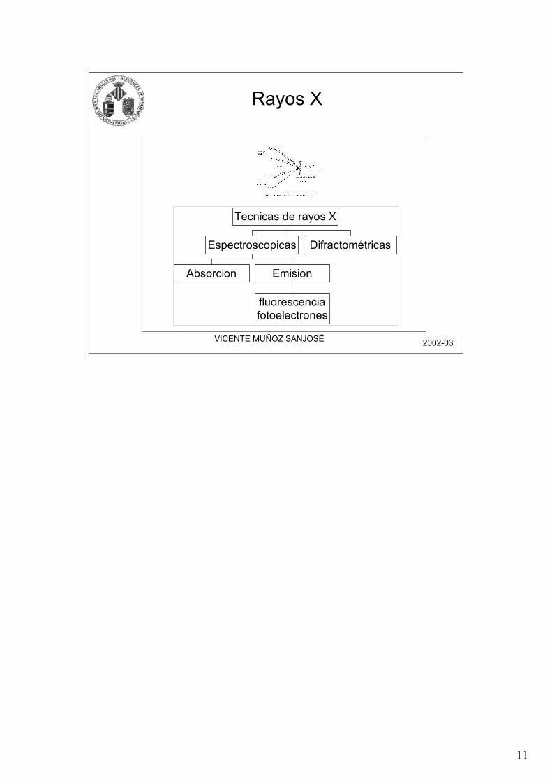
Rayos X

10
VICENTE MUÑOZ SANJOSÉ 2002-03
Absorcion
fluorescenciafotoelectrones
Emision
Espectroscopicas Difractométricas
Tecnicas de rayos X
Rayos X
11
VICENTE MUÑOZ SANJOSÉ 2002-03
Absorcion
fluorescenciafotoelectrones
Emision
Espectroscopicas Difractométricas
Tecnicas de rayos X
Rayos X

12
VICENTE MUÑOZ SANJOSÉ 2002-03
Técnicas de absorción de Rayos X

13
VICENTE MUÑOZ SANJOSÉ 2002-03
Técnicas de emisión de Rayos X

14
VICENTE MUÑOZ SANJOSÉ 2002-03
Métodos generales de difracción de Rayos X

15
VICENTE MUÑOZ SANJOSÉ 2002-03
Rayos XCapas delgadas

16
VICENTE MUÑOZ SANJOSÉ 2002-03
Rayos XCapas delgadas

17
VICENTE MUÑOZ SANJOSÉ 2002-03
Rayos XCapas delgadas

18
VICENTE MUÑOZ SANJOSÉ 2002-03
Rayos XCapas delgadas

19
VICENTE MUÑOZ SANJOSÉ 2002-03
Rayos XCapas delgadas

20
VICENTE MUÑOZ SANJOSÉ 2002-03
Rayos XCapas delgadas

21
VICENTE MUÑOZ SANJOSÉ 2002-03
Rayos XCapas delgadas

22
VICENTE MUÑOZ SANJOSÉ 2002-03
Microscopia Electrónica
TransmisiónBarrido
In theory the resolution of any microscope is limited by the wavelength of the radiation used. The wavelengths of normal light range from about 700 nanometres for red light to 400 nanometres for violet. The light microscope therefore cannot distinguish two features that are less than 400 nanometres apart. Some very ingenious scientists have now made light microscopes that go down to about 100 nanometres by using special tricks but that is about the limit.
The wavelengths of electrons typically lie between 37 picometres for 100 kilovolt electrons to 19 picometres for 300 kilovolt ones (for electrons the wavelength depends on the so-called accelerating voltage; the higher the voltage, the smaller the wavelength). You might expect the TEM to have a resolution near those values - and therefore easily resolve atoms with their sizes of some 0.1nanometres (100 picometres). That is not the case. In reality we have to work very hard to make TEMs reach 0.1 nanometres; a more typical value for an excellent, modern instrument is close to 0.2 nm. This is not because theory is wrong but because we have such terrible lenses in our microscopes. All our lenses are a bit like the Hubble telescope : they suffer from spherical aberration which means that the lens characteristics change as you move from the centre of the lens to the edge. This is not because we are such bad lens designers (or make errors like the Hubble-telescope lens designers) but is inherent to using magnetic fields as electron lenses. In the TEM we are limited by the available magnetic materials. The resolution gets better at higher accelerating voltages but this has practical limits. There are a few microscopes around that go up to one or even three million volts. They are, however, up to several stories (tens of metres) high and their price is that of 10 to 20 normal TEMs.

23
VICENTE MUÑOZ SANJOSÉ 2002-03
SEM
24
VICENTE MUÑOZ SANJOSÉ 2002-03
25
VICENTE MUÑOZ SANJOSÉ 2002-03
26
VICENTE MUÑOZ SANJOSÉ 2002-03

27
VICENTE MUÑOZ SANJOSÉ 2002-03

28
VICENTE MUÑOZ SANJOSÉ 2002-03

29
VICENTE MUÑOZ SANJOSÉ 2002-03

30
VICENTE MUÑOZ SANJOSÉ 2002-03

31
VICENTE MUÑOZ SANJOSÉ 2002-03

32
VICENTE MUÑOZ SANJOSÉ 2002-03

33
VICENTE MUÑOZ SANJOSÉ 2002-03

34
VICENTE MUÑOZ SANJOSÉ 2002-03
SEM

35
VICENTE MUÑOZ SANJOSÉ 2002-03
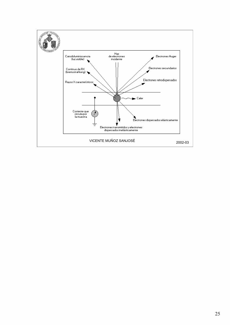
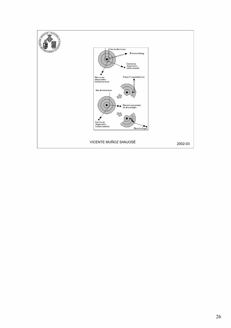
Interacción de electrones con la materia

36
VICENTE MUÑOZ SANJOSÉ 2002-03
Electrón 1 ----- Electrón retrodispersadoElectrón 2 ----- Electrón secundario
RX son los rayos X, característicos del átomo que los ha producido. Nos proporcionan información química elemental de la zona de la muestra de la que proceden. Con esta señal se obtienen los análisis químicos cualitativos y cuantitativos de la composición de la muestra.El proceso físico mediante el cual se produce las tres señales anteriores, en un átomo de la muestra, es el siguiente:
Un electrón 1 del haz primario choca con un electrón 2 de una capa interna del átomo y expulsa a éste de dicho átomo. El átomo queda entonces en un estado excitado ya que el electrón 2 deja una vacante en el nivel energético del que procede. El átomo, para volver a su estado fundamental, de mínima energía, desplaza un electrón 3 de un orbital más energético a la vacante dejada por el electrón 2. Para que tenga lugar este proceso, el electrón 3 se tiene que liberar de una cierta cantidad de energía, igual a la diferencia de losdos niveles energéticos involucrados en el proceso. Esta energía la liberaen forma de rayos X (RX). La vacante dejada por el electrón 3 será posteriormente ocupada por otro electrón de otro nivel más energético, produciéndose otro fotón de RX, yasí sucesivamente. El electrón 2 arrancado del átomo es lo que se denominó en el gráficoanterior un electrón secundario y el electrón 1 que procede del haz primario, un electrón retrodispersado.

37
VICENTE MUÑOZ SANJOSÉ 2002-03
Microscopio electrónico de barrido

38
VICENTE MUÑOZ SANJOSÉ 2002-03
EDAX
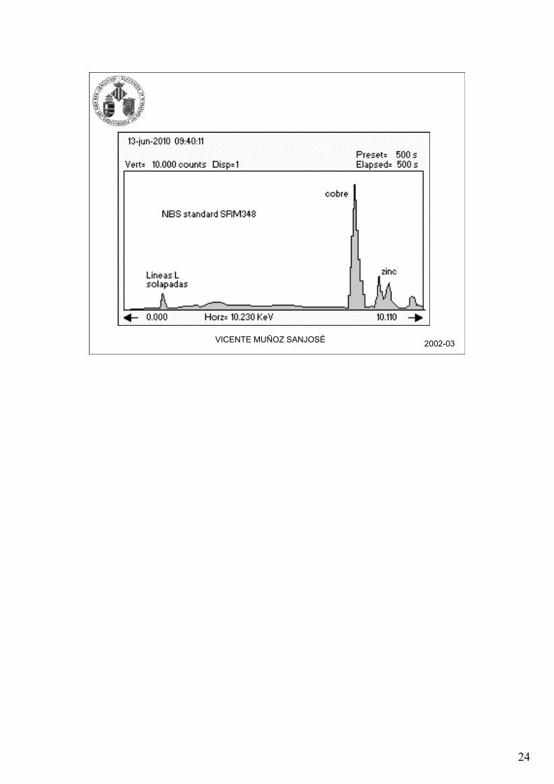
Como puede verse en la figura, un espectro de dispersión de energíasse presenta usualmente como un histograma en donde el eje horizontal son unidades de energía, en Kiloelectronvoltios (KeV), en este caso de 0.00 a 10.240, y el eje vertical número de cuentas o intensidad, en este caso 65536 cuentas la altura total de la escala, que se va autoajustando a medida que crece el número de cuentas de la energía del pico más alto.

39
VICENTE MUÑOZ SANJOSÉ 2002-03
Perfiles de concentración
Perfiles de Concentración y Mapas de RXAdemás de la obtención de un espectro en un punto concreto de la
muestra o en una zona determinada, existen dos formas gráficas de obtener información de la señal de RX: los perfiles de concentración o perfiles de línea y los mapas de RX. Perfiles de concentración .- La técnica consiste en obtener una gráfica de la intensidad de la señal de RX de uno o varios elementos a lo largo de una línea de barrido entre dos puntos de la muestra. Sirve para ver gráficamente como varia la concentración de uno o varios elementos entredos puntos.

40
VICENTE MUÑOZ SANJOSÉ 2002-03
Imagen de electrones retrodispersados

41
VICENTE MUÑOZ SANJOSÉ 2002-03
Imagen de electrones secundarios

42
VICENTE MUÑOZ SANJOSÉ 2002-03
TEM
Penetration
Another issue is penetration. Normal light can travel long distances without being changed much by the material it travels through (unless that material is opaque like metals which absorb most light). In contrast, electrons are strongly affected. In an electron beam going through air, all electrons will have collided with the atoms in the air within one metre of their starting point and there is no electron beam left. To allow the electron beam in the TEM to travel the full length of the column without being stopped, we need to reduce the amount of air as far as we can. This means the electron beam must travel through vacuum. The microscope is therefore equipped with very strong pumps that pump out all the air
A second issue in penetration is the thickness of the specimen (the piece of material we look at in the TEM). If the specimen is not very thin, all electrons will have been scattered away and once again we will have no beam left. How thin the specimens need to be depends on the material. A normal microscope will easily get through 1000 nanometres of a light material like carbon but will have difficulty with 50 nanometres of something heavy like gold.

43
VICENTE MUÑOZ SANJOSÉ 2002-03
Column of a TEMThe cylindrical vessel at the top contains the electron gun (indicated by the green line). The specimen stageor goniometer is found halfway down the column (the red line). The location of the electron lenses is indicated by the blue lines on the left (we'll look at lenses in more detail further on). The vacuum system is found throughout the column
The tungsten filament is a simple piece of tungsten wire with a sharp bend in the middle (light bulb filaments are made from tungsten as well). A high current will heat the filament to about 2700°C, especially at the bend and it will glow white hot. At this point many electrons will make the jump from filament to vacuum. The tungsten filament is the cheapest. A typical filament will work for one or two months and then must be replaced by a new one.
A lanthanum-hexaboride filament is similar to the tungsten filament but with a crystal of lanthanum-hexaboride at the tip. The tungsten wire on which it is mounted is once again heated, but only to 2100°C. The result is a higher-quality electron beam. LaB6 filaments cost about US$ 1000 and typically run for about a year.
The Field Emission Gun (or FEG) is more complicated. Once again there is a tungsten wire. In this case a very thin needle of a tungsten crystal in a special orientation is welded to the wire. There exists a 'cold' FEG where the wire is not heated at all, but in modern FEG instruments the filament is heated to about 1500°C. The temperature makes the electrons 'hop' and thereby helps the real process by which the electrons come out of the sharp tungsten tip : the field emission. We get field emission by putting a second anode very close (one-half millimetre) to the tip (not the main anode with its high voltage of 200 kilovolts; that anode is at a larger distance of about 10 millimetres). The voltage on the second anode is only about 4 kilovolts. The electric field is then so strong that the tip will start emitting electrons. FEG's typically last one to several years.

44
VICENTE MUÑOZ SANJOSÉ 2002-03
•Bright field : the standard method of recording TEM images. •Diffraction : a difficult to understand but very useful method for getting information about crystals. •Dark field : a second often-used imaging method. •High-resolution TEM imaging : (too) simply stated, a way of 'seeing atoms'. •Analysis : providing the chemical composition of the material we are looking at.
Methods in TEM

45
VICENTE MUÑOZ SANJOSÉ 2002-03
Bright fieldDark field

46
VICENTE MUÑOZ SANJOSÉ 2002-03
Diffraction

47
VICENTE MUÑOZ SANJOSÉ 2002-03
Ejemplo de microscopia TEM

48
VICENTE MUÑOZ SANJOSÉ 2002-03
High-resolution TEM imaging
High-resolution image of silicon displaying dumbbells (pairs of silicon atom columns). The distance between the atom columns in a dumbbell is 0.14 nanometres. The real structure is drawn in colour (the green lines are used to highlight the arrangement and have no direct meaning).

49
VICENTE MUÑOZ SANJOSÉ 2002-03
Analysis

50
VICENTE MUÑOZ SANJOSÉ 2002-03
Twins and dislocations
TEM image of dislocations (only one in this small detail, three in the full-size image) at the interface between gallium-arsenide (dark area at bottom) and silicon (top). The dislocation (the extra half-plane in silicon) can be found by following the line in the crystal structure indicated by the black marker downwards.

51
VICENTE MUÑOZ SANJOSÉ 2002-03
Microscopía de efecto tunel

52
VICENTE MUÑOZ SANJOSÉ 2002-03
STM

53
VICENTE MUÑOZ SANJOSÉ 2002-03
................................. Microscopía de fuerzas atómica

54
VICENTE MUÑOZ SANJOSÉ 2002-03
rug = 0.35 nmparece que también hay unadirección marcada
los clusters son mucho más pequeños que en la muestra CTGA30a-b
escalón de ~5 Å
Microscopía de fuerzas atómica

55
VICENTE MUÑOZ SANJOSÉ 2002-03
ZnO