Technology Brief 7 Integrated Circuit Fabrication Process
4
136 TECHNOLOGY BRIEF7: INTEGRATED CIRCUIT FABRICATION PROCESS Technology Brief 7 Integrated Circuit Fabrication Process Do you ever wonder how the processor in your computer was actually fabricated? How is it that engineers can put hundreds of millions of transistors into one device that measures only a few centimeters on a side (and with so few errors) so the devices actually function as expected? Devices such as modern computer processors and semiconductor memories fall into a class known as integrated circuits (IC). They are so named because all of the components in the circuit (and their “wires”) are fabricated simultaneously (integrated) onto a circuit during the manufacturing process. This is in contrast to circuits where each component is fabricated separately and then soldered or wired together onto a common board (such as those you probably build in your lab classes). Integrated circuits were first demonstrated independently by Jack Kilby at Texas Instruments and Robert Noyce at Fairchild Semiconductor in the late 1950s. Once developed, the ability to easily manufacture components and their connections with good quality control meant that circuits with thousands (then millions, then billions) of components could be designed and built reliably. Semiconductor Processing Basics All mainstream semiconductor integrated-circuit pro- cesses start with a thin slice of silicon, known as a substrate or wafer.This wafer is circular and ranges from 4 to 18 inches in diameter and is approximately 1 mm thick (hence its name). Each wafer is cut from a single crystal of the element silicon and polished to its final thickness with atomic smoothness (Fig.TF7-1). Most circuit designs (like your processor) fit into a few square centimeters of silicon area; each self-contained area is known as a die. After fabrication, the wafer is cut to produce independent, rectangular dies often known as chips, which are then packaged with plastic covers and metal pins or other external connections to produce the final component you buy at the store. A specific sequence or process of chemical and mechanical modifications is performed on certain areas of the wafer. Although complex processes employ a variety of techniques, a basic IC process will employ one of the following three modifications to the wafer: Figure TF7-1: A single 4-inch silicon wafer. Note the wafer’s mirror-like surface. (Courtesy of Veljko Milanovic.) • Implantation: Atoms or molecules are driven into (implanted in) the silicon wafer, changing its elec- tronic properties (Fig. TF7-2(a)). • Deposition: Materials such as metals, insulators, or semiconductors are deposited in thin layers (like spray painting) onto the wafer (Fig. TF7-2(b)). • Etching: Material is removed from the wafer through chemical reactions or mechanical motion (Fig. TF7-2(c)). Lithography When building an IC, we need to perform different modifications to different areas of the wafer. We may want to etch some areas and add metal to others, for example. The method by which we define which areas will be modified is known as lithography.
Transcript of Technology Brief 7 Integrated Circuit Fabrication Process

“book” — 2015/5/4 — 7:08 — page 136 — #22
136 TECHNOLOGY BRIEF 7: INTEGRATED CIRCUIT FABRICATION PROCESS
Technology Brief 7Integrated Circuit FabricationProcess
Do you ever wonder how the processor in your computerwas actually fabricated? How is it that engineers can puthundreds of millions of transistors into one device thatmeasures only a few centimeters on a side (and with sofew errors) so the devices actually function as expected?
Devices such as modern computer processors andsemiconductor memories fall into a class known asintegrated circuits (IC). They are so named becauseall of the components in the circuit (and their “wires”)are fabricated simultaneously (integrated) onto a circuitduring the manufacturing process. This is in contrast tocircuits where each component is fabricated separatelyand then soldered or wired together onto a common board(such as those you probably build in your lab classes).Integrated circuits were first demonstrated independentlyby Jack Kilby at Texas Instruments and Robert Noyceat Fairchild Semiconductor in the late 1950s. Oncedeveloped, the ability to easily manufacture componentsand their connections with good quality control meantthat circuits with thousands (then millions, then billions)of components could be designed and built reliably.
Semiconductor Processing Basics
All mainstream semiconductor integrated-circuit pro-cesses start with a thin slice of silicon, known as asubstrate or wafer.This wafer is circular and ranges from4 to 18 inches in diameter and is approximately 1 mm thick(hence its name). Each wafer is cut from a single crystalof the element silicon and polished to its final thicknesswith atomic smoothness (Fig.TF7-1).Most circuit designs(like your processor) fit into a few square centimeters ofsilicon area; each self-contained area is known as a die.After fabrication, the wafer is cut to produce independent,rectangular dies often known as chips, which are thenpackaged with plastic covers and metal pins or otherexternal connections to produce the final component youbuy at the store.
A specific sequence or process of chemical andmechanical modifications is performed on certain areas ofthe wafer. Although complex processes employ a varietyof techniques, a basic IC process will employ one of thefollowing three modifications to the wafer:
FigureTF7-1: A single 4-inch silicon wafer. Note the wafer’smirror-like surface. (Courtesy of Veljko Milanovic.)
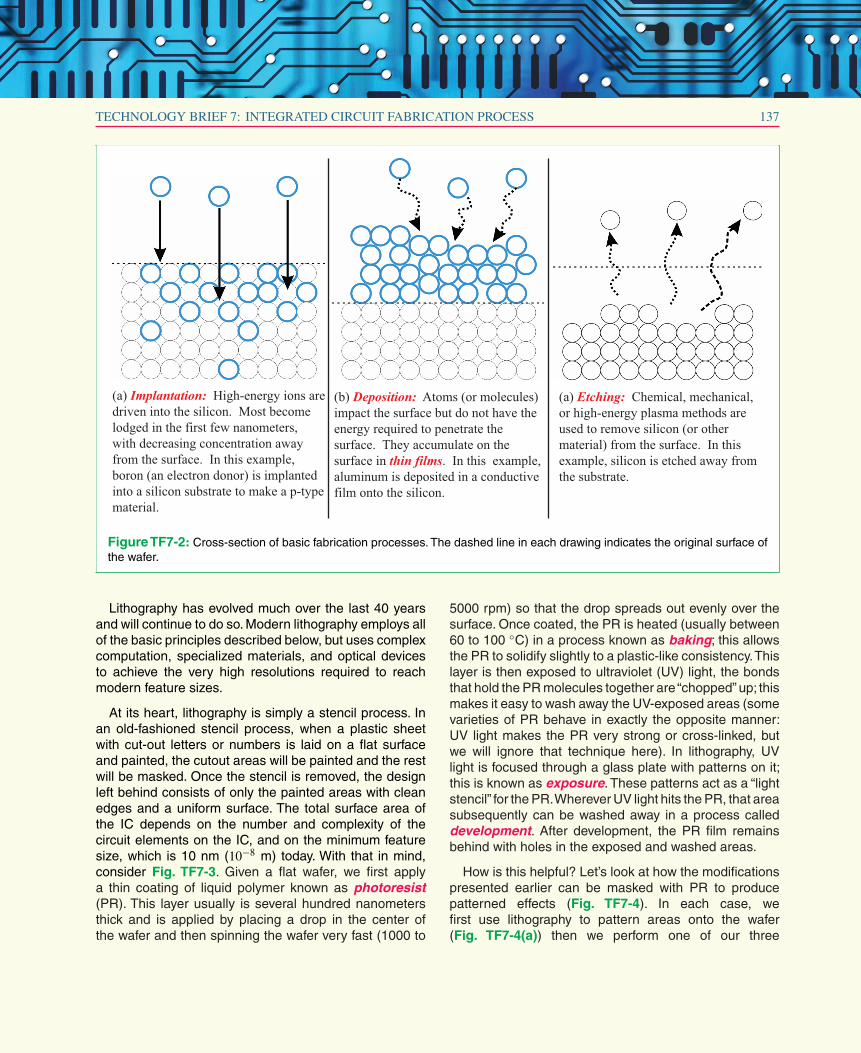
• Implantation: Atoms or molecules are driven into(implanted in) the silicon wafer, changing its elec-tronic properties (Fig. TF7-2(a)).
• Deposition: Materials such as metals, insulators,or semiconductors are deposited in thin layers (likespray painting) onto the wafer (Fig. TF7-2(b)).
• Etching: Material is removed from the waferthrough chemical reactions or mechanical motion(Fig. TF7-2(c)).
Lithography
When building an IC, we need to perform differentmodifications to different areas of the wafer. We maywant to etch some areas and add metal to others, forexample. The method by which we define which areaswill be modified is known as lithography.
“book” — 2015/5/4 — 7:08 — page 137 — #23
TECHNOLOGY BRIEF 7: INTEGRATED CIRCUIT FABRICATION PROCESS 137
(a) Implantation: High-energy ions are driven into the silicon. Most become lodged in the first few nanometers, with decreasing concentration awayfrom the surface. In this example, boron (an electron donor) is implanted into a silicon substrate to make a p-typematerial.
(b) Deposition: Atoms (or molecules)impact the surface but do not have the energy required to penetrate thesurface. They accumulate on thesurface in thin films. In this example, aluminum is deposited in a conductive film onto the silicon.
(a) Etching: Chemical, mechanical,or high-energy plasma methods areused to remove silicon (or othermaterial) from the surface. In thisexample, silicon is etched away fromthe substrate.
FigureTF7-2: Cross-section of basic fabrication processes. The dashed line in each drawing indicates the original surface ofthe wafer.
Lithography has evolved much over the last 40 yearsand will continue to do so. Modern lithography employs allof the basic principles described below, but uses complexcomputation, specialized materials, and optical devicesto achieve the very high resolutions required to reachmodern feature sizes.
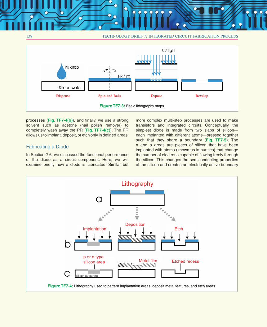
At its heart, lithography is simply a stencil process. Inan old-fashioned stencil process, when a plastic sheetwith cut-out letters or numbers is laid on a flat surfaceand painted, the cutout areas will be painted and the restwill be masked. Once the stencil is removed, the designleft behind consists of only the painted areas with cleanedges and a uniform surface. The total surface area ofthe IC depends on the number and complexity of thecircuit elements on the IC, and on the minimum featuresize, which is 10 nm (10−8 m) today. With that in mind,consider Fig. TF7-3. Given a flat wafer, we first applya thin coating of liquid polymer known as photoresist(PR). This layer usually is several hundred nanometersthick and is applied by placing a drop in the center ofthe wafer and then spinning the wafer very fast (1000 to
5000 rpm) so that the drop spreads out evenly over thesurface. Once coated, the PR is heated (usually between60 to 100 ◦C) in a process known as baking; this allowsthe PR to solidify slightly to a plastic-like consistency.Thislayer is then exposed to ultraviolet (UV) light, the bondsthat hold the PR molecules together are “chopped” up; thismakes it easy to wash away the UV-exposed areas (somevarieties of PR behave in exactly the opposite manner:UV light makes the PR very strong or cross-linked, butwe will ignore that technique here). In lithography, UVlight is focused through a glass plate with patterns on it;this is known as exposure. These patterns act as a “lightstencil” for the PR.Wherever UV light hits the PR, that areasubsequently can be washed away in a process calleddevelopment. After development, the PR film remainsbehind with holes in the exposed and washed areas.
How is this helpful? Let’s look at how the modificationspresented earlier can be masked with PR to producepatterned effects (Fig. TF7-4). In each case, wefirst use lithography to pattern areas onto the wafer(Fig. TF7-4(a)) then we perform one of our three
“book” — 2015/5/4 — 7:08 — page 138 — #24
138 TECHNOLOGY BRIEF 7: INTEGRATED CIRCUIT FABRICATION PROCESS
Dispense Spin and Bake Expose Develop
Figure TF7-3: Basic lithography steps.
processes (Fig. TF7-4(b)), and finally, we use a strongsolvent such as acetone (nail polish remover) tocompletely wash away the PR (Fig. TF7-4(c)). The PRallows us to implant, deposit, or etch only in defined areas.
Fabricating a Diode
In Section 2-6, we discussed the functional performanceof the diode as a circuit component. Here, we willexamine briefly how a diode is fabricated. Similar but
more complex multi-step processes are used to maketransistors and integrated circuits. Conceptually, thesimplest diode is made from two slabs of silicon—each implanted with different atoms—pressed togethersuch that they share a boundary (Fig. TF7-5). Then and p areas are pieces of silicon that have beenimplanted with atoms (known as impurities) that changethe number of electrons capable of flowing freely throughthe silicon. This changes the semiconducting propertiesof the silicon and creates an electrically active boundary
silicon substrate
p or n typesilicon area Metal film
ImplantationDeposition
Lithography
Etch
Etched recess
Figure TF7-4: Lithography used to pattern implantation areas, deposit metal features, and etch areas.
“book” — 2015/5/4 — 7:08 — page 139 — #25
TECHNOLOGY BRIEF 7: INTEGRATED CIRCUIT FABRICATION PROCESS 139
p-typesilicon
n-typesilicon
metalmetal
Figure TF7-5: The basic diode (top) circuit symbol and(bottom) conceptual depiction of the physical structure.
a
b
c
d
e
f
g
h
i
j
Lithography + etch oxide
Remove PR
p-type implant
Grow oxide
n-type implant Lithography + etch oxide
Remove PR
Metal deposition
Lithography + etch metal
Complete diode
Metal Metal
Figure TF7-6: A simple pn-junction diode fabricationprocess.
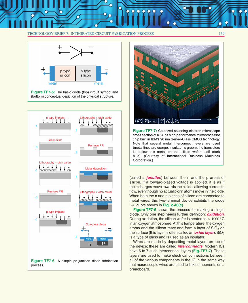
Figure TF7-7: Colorized scanning electron-microscopecross section of a 64-bit high-performance microprocessorchip built in IBM’s 90 nm Server-Class CMOS technology.Note that several metal interconnect levels are used(metal lines are orange, insulator is green); the transistorslie below this metal on the silicon wafer itself (darkblue). (Courtesy of International Business MachinesCorporation.)
(called a junction) between the n and the p areas ofsilicon. If a forward-biased voltage is applied, it is as ifthe p charges move towards the n side, allowing current toflow, even though no actual p or n atoms move in the diode.When both the n and p pieces of silicon are connected tometal wires, this two-terminal device exhibits the diodei–υ curve shown in Fig. 2-40(c).
Figure TF7-6 shows the process for making a singlediode. Only one step needs further definition: oxidation.During oxidation, the silicon wafer is heated to > 1000 ◦Cin an oxygen atmosphere. At this temperature, the oxygenatoms and the silicon react and form a layer of SiO2 onthe surface (this layer is often called an oxide layer). SiO2is a type of glass and is used as an insulator.
Wires are made by depositing metal layers on top ofthe device; these are called interconnects. Modern ICshave 6 to 7 such interconnect layers (Fig. TF7-7). Theselayers are used to make electrical connections betweenall of the various components in the IC in the same waythat macroscopic wires are used to link components on abreadboard.