Techniques for Testing Integrated Circuits - Semantic Scholar · Research Projects Agency, ARPA...
141
Techniques for Testing Integrated Circuits Thesis by Erik P. DeBenedictis In Partial Fulfillment of the Requirements for the Degree of Doctor of Philosophy California Institute of Technology Pasadena, California 1983 submitted 5 May 1982
Transcript of Techniques for Testing Integrated Circuits - Semantic Scholar · Research Projects Agency, ARPA...

Techniques for Testing Integrated Circuits
Thesis by
Erik P. DeBenedictis
In Partial Fulfillment of the Requirements
for the Degree of
Doctor of Philosophy
California Institute of Technology
Pasadena, California
1983
submitted 5 May 1982

Ii
Acknowledgments
Chuck Seitz and Carver Mead are the persons most deserving of acknowledgment. Chuck
and Carver have worked closely with me on this testing research since 1979, giving me their
ideas and making suggestions about mine. Chuck has also been very helpful in the
preparation of this document, having given extensive suggestions about its technical and
grammatical content.
Please let me express here my appreciation to the ARPA management both for their help in
providing an environment whereby ideas can be shared among the university community, and
for their support of this research. This research was supported by the Defense Advanced
Research Projects Agency, ARPA Order number 3771, and monitored by the Office of Naval
Research under contract number N00014-79-C-0597.

iii
Abstract
A language is presented for describing tests of integrated circuits. The language has a
high abstractive capability that enables test specifications to follow the structural or logical
organization of a design. The test language is applied to a number of current design styles in
a series of examples. Methods for designing integrated circuits for testability are
demonstrated. An implementation of the test language through a test language interpreter
and a tester is discussed. Tester designs are presented that will execute the test language
with unusually high efficiency.

iv
Table of Contents1. Introduction 1
1.1 A Tour Through the Design of an Integrated Circuit 21.1.1 Initial Design and Testing 2
1.1. 1.1 Description of the Pins 21.1.1.2 Initial Checkout 31•1.1.3 Common Errors 5
1.1.2 Exhaustive Checkout 61.1.3 Testing an Adder as an Arithmetic Array 81.1.4 Testing When Embedded in a System 9
1.1.4.. 1 Describing an Access Procedure 101.1.4.2 Testing a Part Through an Access Procedure 11
1.2 Strategy for the Design of Tests and Design for Testability 131.2.1 Primitive Tests 131.2.2 Application of Primitive Tests 131.2.3 Synergism of Testing and Design 141.2.4 Testability 14
1 .3 The Design of Testers 151.3.1 Test Generation Modes 151.3.2 Tester Construction for the Test Language 171.3.3 Interface of the Test Language to Simulators 17
1.4 The Value of an Interactive, Non-Embedded Test Language 191.4.1 ATLAS 191.4.2 FACTOR 201.4.3 ANGEL 201.4.4 The FIFI Test Language 21
1.5 Summary 212. A Notation for Describing Integrated Circuit Testing 22
2.1 Abstract Elements of Digital Electrical Signals 222.1.1 Elements of the Algebra 222.1.2 Ports 242.1.3 Equations and Assignments 24
2.1.3.1 Assignments 252.1.3.2 Expressions 25
2.1.4 Specification of Analog Tests 282.2 Organization of Digita.l Manipulations into Test Matrices 28
2.2.1 A Restricted Test Language and Testing Efficiency 292.2.2 Elements 312.2.3 Test Matrices 312.2.4 Static Interpretation 332.2.5 Dynamic Interpretation 35
2.3 Test Language Procedures 382.3.1 Procedure Defining and Calling Notations in Programming Languages 392.3.2 Procedure Conventions in the Test Language 392.3.3 Sophisticated Interpretation of the Interrogate Action 41
2.3.3.1 Simple Interpretation of the Interrogate Action 422.3.3.2 A More Complex Interpretation of the Interrogate Action 42
2.3.4 Timing 44

v
3. Examples of the Test Language3.1 Abstraction of a Bidirectional Data Bus3.2 Performing Complex Data Manipulations3.3 Testing a 16K Dynamic Random Access Memory3.4 Multiphase Clocking and the Test Language3.5 An Example of the Test Generation Technique for Large Systems
3.5~1 Testing the Data Path Unit3.6 Testing a Microprogrammed System vllith a Data Path
3.6.1 Data Path Part3.6.2 Microcode Part3.6.3 State Latch Part
4. Testing of Sequential Systems4.1 Previous Approaches to Sequential Testing
4.1.1 Conventional Testing of Combinational Networks4.1.2 New Methods for Testing Sequential Devices4.1.3 LSSD4.1.4 Testing Art4.1 .5 Other Methods
4.2 Structured Design and Design for Testability4.2.1 The Value of Structured Design4.2.2 Structured Integrated Circuit Design4.2.3 Testing Structured Designs with Access Procedures4.2.4 A Filter Model
4.2.4.1 Controllability and Observability in the Fitter Model4.2.5 Access Procedures as an Inverse Filter Function4.2.6 Definition of an Access Procedure
4.3 Using the Test Language to Describe General Behavior4.3.1 The Actions of a Part Upon a Port
4.3.1.1 The Actions of a Tester4.3.2 The Duality of Actions Upon a Port4.3.3 The Behavior of Groups of Ports4.3.4 Repetition4.3.5 Relationships Between Styles of System Descriptions4.3.6 Examples of Behavioral Descriptions
4.3.6.1 A Four Bit Adder4.3.6.2 A D-type Flip Flop
4.4 Deriving Access Procedures from Behavioral Descriptions4.4.1 Accessibility Through Flip Flops4.4.2 Accessibility Through A Scan Path4.4.3 A Method for Generating Access Procedures4.4.4 Matching Access Procedures with Tests
4.5 Controlled Expansion of Test Vectors4.5.1 Number of Test Vectors in a Test4.5.2 Asymptotic Dependence of Test Size on Number of Cells4.5.3 Improvements on Asymptotic Behavior
4.5.3.1 Reducing the Length of Access Procedures4.5.3.2 Changing the Branching Factor4.5.3.3 Size of Primitive Cells
464648495255565859616163636465666667686869707172737374747475767777797980808183858586868788888990

vi
4.5.4 Actual Dependence of Test Size Upon Chip Size4.6 A Perspective on Structured Compositions
4.6.1 Design by Composition4.6.2 Composition by Concatenation4.6.3 Design by Recursion4.6.4 A Numerical Comparison of Testing Strategies4.6.5 Other Hierarchical Compositions4.6.6 Serial and Parallel Testing
4.7 Conclusions5. The FIFI Test System: A Reality Test
5.1 Test System Commands5.1.1 !Loading Test Programs: Define Command5.1.2 Executing Test Programs: Execute and Immediate Commands5.1.3 Miscellaneous Commands
5.2 Some Examples of the Test Language5.2.1 Testing the Adder in a Z80 Microprocessor5.2.2 Testing Instruction Decoding in a Z80 Microprocessor5.2.3 Reading the ROM of an 8041
6. The Design of Test Instruments6.1 Constrained Tests and Tester Design6.2 High Performance Test Instruments
6.2.1 Conventional Tester Design6.2.2 Areas for Improvement6.2.3 Efficient Use of Test Vector Storage6.2.4 Interface of the Tester Model to the Test Language6.2.5 Further Refinements in Tester Design6.2.6 Analogy of Tester Design to the Design of .computers
6.2.6.1 Virtual Memory vs the Test Vector Buffer6.3 Requirements for Test Instruments
7. ConclusionsA. Syntax of the Test Language
A.1 User C.ommandsA.2 Procedure DeclarationsA.3 Port DeclarationsA.4 Typed Value ExpressionsA.5 Expressions
Index
91929393959698
100.101102102103103104105105109111
114114115115116117118119120120121123125126126127127128134

1
1. Introduction
This thesis describes the results of an investigation into systematic methods for testing
integrated circuits. The central result is a language for describing tests. In the formal
presentation. of the language, in chapter 2, the ability of the language to represent tests of
integrated circuits in the same abstract manner that their designs are visualized is
emphasized. The remainder of this document is an exploration and verification of the
language's ability to solve a number of the problems of testing integrated circuits. In
chapter 1 the usefulness of the language as an interactive tool for the design and debugging
of integrated circuits is illustrated. In chapter 3 the ability of the language to describe test
of real systems is demonstrated through examples applied to integrated circuits designed
with different design styles. In chapter 4 the methods used to generate the examples of
chapter 3 are discussed and their general applicability is explored. Chapter 5 describes an
implementation of the language. Finally, in chapter 6 a tester design is proposed that can
execute the test language more efficiently than conventional testers. The result of this
analysis is general technique for designing integrated circuits and their tests that yields
reliable results with a predictable amount of effort.
The abstractive properties of the language are aimed at formalizing ~he manner of testing
integrated circuits that is in use today. It has been observed that informally generated tests
follow a physical structure (either real or imagined) of the device under test. The
specifications of these tests do not generally appear to h~ve any structure, however. It is
conjectured that the reason the test specifications do not reflect the structure of the
design is that existing test languages do not have the necessary abstractive capabilities.
The test language proposed in this thesis attempts to provide this capability.

2
1.1' A Tour Through the Design of an Integrated Circuit
To gain a perspective into the nature of testing complex integrated circuit systems and as
an informal introduction to the test language, this section will follow the design and testing
of a small portion of a complex integrated circuit. As a demonstration of the test system, let
us follow the development of an interesting part, an adder, in an integrated circuit.
A common technique in the design of a complex system is to design and test many of the
component parts separately and then simply compose them into a much larger system. This
technique can be applied to integrated circuit design: a part, such as a memory cell, error
correction unit, or adder, can initially be designed alone, then tested or simulated with a
prototype integrated circuit, and finally incorporated into its environment in the system.
1.1 •1 Initial Design and Testing
In the earliest stages our adder is on a prototype chip with all of the inputs and outputs,
and possibly some test points, connected to pads. The design of this chip must be verified.
1.1.1.1 Description of the Pins
Testing can start off immediately with the prototype chip. Figure 1-1 illustrates such a
chip. The designer would place the chip into the tester and run the test system. Before
testing can begin some preliminary description of the chip must be made: the pins must be
described. This operation might appear as follows:
FIFI>define port a 1 2 3 4;FIFI>define port b 5 6 7 8;FIFI>define port c 9 '10 11 12;
definitions of pins
An interactive implementation of the test language described here has been constructed
and called FIFI. The FIFI> at the beginning of each line is representative of the prompting
that the test system supplies. The underlined boldface text is the test language input.

3
aI I
I I I IV V V V
+---+-+-+-+----+I II +----->I adder +-----> ct +----->I +----->I I+---+-+-+-+----+
t t t tI I I II I I I
b
Figure 1-1: Illustration of a Prototype Chip
Examples of the test language preceded with FIFI> can generally be typed directly to the
test language interpreter. Descriptive information placed to the right in an italic typeface is
not part of the test language. These commands specify that there are· three logical signals
that go in or out of the chip: a, b, and c. Each of these three signals consists of four wires or
conductors, and the numbering of these conductors is as shown above.
1.1.1.2 Initial Checkout
At this point the function of the prototype chip can be tested. The designer can imagine
some inputs that will produce understandable outputs. If the chip were an adder, for
example, it might be useful to verify that 2+2 works before an exhaustive functional and
timing test is performed. If 2+2 does not generate 4, then a more comprehensive test will be
worthless. Similarly, if a chip intended to perform error correction failed to recognize
error-free data, then backtracking and carefully inspecting the design would be advisable.
The designer continues his initial testing with:

FIFI>i a<2,b<2;FIFI>i c!;c:1S--FIFI>i a<O,b<2;FIFI>i c!;c:1S--
4
line 1line 2line 3line 4line 5line 6
Lines 1, 2, 4, and 5 start with the letter i. The i is an abbreviation of the word immediate
that indicates that the remainder of the line is to be executed immediately. The first line
contains two commands of the form p<e. These commands cause the tester to drive a
voltage into the pins previously defined. The word on the left, P, is the name of a previously
declared port, and the number (in general, an expression e) on the right is a value that will
be driven to the pins. The operator < is like an arrow pointing from the expression to the
port, indicating the direction of signal flow. The second line invokes immediate execution of
the single command cr. Again, the word on the left, c, represents a port declared above, but
the operator! causes the tester to print the voltage on those pins instead of driving the pin.
The third line is a report of the value of that port.
Although these commands appear to be executed immediately, it is the semicolon at the
end of each line that invokes the test steps. Where no ; appears at the end of a line the
test stap would be deferred until one was encountered, similarly multiple ;IS on the same line
will cause multiple test steps. The commands are executed in between the time when the
return key on the terminal is pressed and the next prompt is printed.
Notice on the third line that the tester is reporting the value of the c port as 15 (decimal),
meaning that all four pins have a high voltage.
Having observed the result of 2+2, the values 2+0 are tried. The tester responds again
with the result 15, or all pins high.

5
1.1.1.3 Common Errors
The 2+2 test did not generate the proper response. The designer then tries 2+0, and
again gets an improper response. At this point the following thoughts pass through the
designer1s mind:
1. Both responses were 15, and 1 5 corresponds to all wires high. Anunconnected wire will read as high, and therefore perhaps the chip is not inthe socket.
2. If the power supplies were not connecteds not bonded, or corrupted inside thechip then all the outputs would float, causing the observed response.
3. Perhaps the assumption that a and b are inputs and c is the output isincorrect, and actually a or b is the output and c is an input. The tester wouldthen be monitoring an input port and would read high.
After considering these possibilities, the designer checks the chip, the power supplies and
the layout to determine if any of the above is responsible. He discovers that, in fact, the
ground lead is disconnected. The 2+2 test is repeated:
FIFI>i a<2,b<2;FIFI>i elja:1FIFI>i a{2,b{O;FIFI>i e!ja:O
Considerable success: one of the outputs has been observed in both the high and low,
state in response to changes in inputs. This gives reason to believe that the power supply
is intact and that the output drivers function. Otherwise, however, the outputs are all wrong
(this is an adder and the result of 2+2 should be 4).
Now the designer draws a picture to see what is happening:
2 +2 =1??
binary
eel aeel ee eel
2 +e =2??
binary
o e 1 ee e e eeel e

6
This picture looks like addition with the binary order of bits reversed. Therefore, the
designer checks the layout to verify this possibility, discovers the mistake, and then
changes the port definitions with the following commands:
FIFI>define port a 4 3 2 1;FIFI>define port b 8 7 6 5;FIFI>define port c 12 11 10 9;FiFI>i a<2,b<2;FIFI>i c!;a:4 --FIFI>i a<2,b<O;FIFI>i c!;a:2
conductors reversed
The test system is used like a pocket calculator: short expressions can be entered and
the results can be observed immediately. In the above example, the designer tried 2+2 and
2+0 and received the correct response.
1.1.2 Exhaustive Checkout
It is now possible to check the adder in considerable detail more-or-Iess automatically.
Assume that a functional simulation of the device produced a table of inputs and expected
responses in the following form: 1
a<3, b<4, c>7;a<4, b<5, c>9;8<5, b<6, c>11;...etc...
Here, the symbol > indicates that the output of the chip, or port, on the left of the
operator is to be sensed and compared with the value on the right. The value on the right is
not altered; if there is a difference a global check fail flag is set.
1This is not as contrived as it may seem: it will later be shown that this notation is anefficient notation to describe simulations.

7
The input output relationship shown here can be applied to the chip by editing the table
shovlin above to the following form and then executing the following tester commands:
contents of file demodefine procedure demo
a<3,b<4,c>7;a<4,b<5,c>9;a<5,b<6,c>11 ;...etc...
end
FIFI>read demoFIFI>execute demo[check failed]FIFI>
declarationbody of procedure
file is readdemo is executedprinted only if bad
The list of inputs and expected responses has been altered in a mechanical way to make
a procedure definition. The procedure definition is read to the test system and the
procedure name '(demo) is made available as an executable test routine. In the example
shown, at least one of the comparisons (indicated with a » failed, causing the statement
[check failed] to be printed.
Another technique for functional checkout is to let the tester algorithmically generate a
test. Consider, for example, testing an adder exhaustively.
FIFI>immediate (loop i 0 15FIFI> (loop j 0 15FIFI> a<i,b<j,c>(i+j)&15;»FIFI>
i takes values 0 1 2 ...13 14 15
& is logical andno [checK fail] printed
Here the two loop statements cause the controlled variables to take values 0-15, and the
third statement performs the test. The third statement uses the loop indices to generate all
possible inputs, and uses the ability of the tester to evaluate simple expressions to
generate the expected response of the adder. Since the message [check failed] was not
printed, the operation of the adder is correct.

8
, .1.3 Testing an Adder as an Arithmetic Array
The exhaustive test shown above is an efficient test for an adder only if the adder is
very small. A larger adder, say 16 bits, would require over four billion test steps. The key to
developing a more efficient test for an adder is to test each of its parts separately.
Complex devices are generally composed of a number of simpler devices that can be tested
independently. The independent testing of all the simpler devices and the verification that
they are connected properly is a proper test for their composition. Adders are usually
constructed as an array of single bit full adders, and this structure will be exploited to aid in
testing.
Figure 1-2 illustrates a four bit adder constructed as an array of full adder stages. Each
adder stage has three inputs, labeled A, B, and ci (carry input), and two outputs, labeled C
(sum), and co (carry out).
v v v v v v v V
+-+--+-+ +-+--+-+ +-+--+-+ +-:+--+-+I A B I I A B I I A B I I A B II ci+<---+co ci+<---+co ci+<---+co II C I I C I C I C I+--+---+
Iv
+--+---+Iv
+--+---+Iv
+--+---+Iv
Figure 1-2: Four Bit Adder as an Arithmetic Array
Each stage could be tested as follows if the stage were directly available to the tester:
FIFI>(loop i 0 1FIFI> (loop j 0 1FIFI> (loop k 0 1FIFI> A<i,B<j,ci<k,FIFI> C>O+j+k)[O],FIFI> co>O+j+k)[1];»))
all combinations of ijand k
[n] is bit extraction[0] is Isb[1] is carry
It is not possible to access the ports ci and co directly, however. These ports can only be

9
accessed through the stages before and after the stage under test. For example, the ci
input to stage N can be set to state x by applying x to both A and B of stage N-1. Using this
strategy the following tester code will test all the adder stages except the first and last:
FIFI>Ooop x 1 2FIFI>FIFI>FIFI>FIFI>FIFI>FIFI>
stages 1 to n-1
<< is shift left
The first stage cannot be tested this way due to its not having a carry input. Similarly the
last stage cannot be tested because of lack of carry output. The following code would be
required to test these:
FIFI>(loop i 0 1FIFI> (loop j 0 1FIFI> A<i,B<j,C>i+j;»FIFI>Ooop i 0 1FIFI> (loop j 0 1FIFI> (loop k 0 1FIFI> A<(i<(3)+(k<(2),FIFI> B<O«3)+(k«2),FIFI> C>(i+j+k)[O]<<3;»)
test first stage
test last stage
1.1.4 Testing When Embedded in a System
Once our adder has been verified functionally and tested as a separate part, it will be
incorporated in its system environment. When put into a new environment testing must again
be performed to verify that its composition into the new system is correct, not to mention
production testing when the final system design has been verified.
When the adder is not available on a prototype chip, with all it inputs and outputs
conveniently available, but embedded in a complex system, verification becomes considerably
more difficult.

10
The strategy to test our adder is to develop a set of software tools to effectively remove
the system surrounding the part and then to apply the same tests as before. In other words,
we create a software tool that can transform a test of a part into an equally valid test of
that part when it is embedded in a system.
Let us imagine that our adder is embedded in a system with a structure of a conventional
one-address accumulator computer; that is, one input of the adder is from an accumulator,
and the output always goes to the accumulator. Furthermore, assume that the accumulator
contains a scan path that can be used for testing purposes. This structure is illustrated
below:
Iselk 1 sinI V
+----------+ 1 +--------+I adder I +-->1
INP ------------>+ inp a I Ilout e +------->+ ACC +------+-------->
+-->+ inp b I I 1 1I 1 I +-->1 1 II +----------+ I +--------+ II 1 1 I+-------------------)--------)----------+
1 Ilelk V SQut
1.1.4.1 Describing an Access Procedure
Considering the particular structure of the device shown, the procedure to apply a set of
stimuli to the band c inputs and to observe the a output is as follows: load the c input into
the ACC through the scan path, apply the b input to the adder and load the ACC with the
result, then unload the a result from the accumulator through the scan path.
A procedure can be constructed to apply two input values and compare one output value
to the adder:

FIFI>procedure accessFIFI> var abc;FIFI> (loop i 0 3 srn<c[i],scrk<1 ;FIFI> sclk<O;)FIFE> INP<b,clk<1 ;FIFI> clk<O;FIFE> (loop i 0 3 sout>a.[i],sclk<1;FIFI> sclk(Oj)FIFI>end
1 1
line 1line 2line 3line 4line 5line 6line 7line 8line 9
Lines 1 and 2 declare a procedure with three arguments, a, b, and c. Lines 3 and 4 cause
one bit at a time (indicated by the bit subscript [i]) of the c argument to be shifted into the
accumulator via the scan path. Lines 5 and 6 cycle the system, causing the adder to be
exercised and the result to be put into the accumulator. Lines 7 and 8 unload the
accumulator serially and compare the value with the expected result.
1.1.4.2 Testing a Part Through an Access Procedure
Having described how to access the adder, the testing can proceed exactly as if the part
were constructed separately. The syntax and semantics of the test language have been
chosen to allow the same test description to generate tests either of a directly accessible
part, or an embedded part.
The exact syntax required to test the adder when embedded in the system is shown
below:
FIFI>(call accessFIFf> a<3,b<4,c>7;FIFI> a<4,b<5,c>9;FIFI> a<5,b<6,c>11;FIFI> mete...)
line 1line 2line 3line 4line 5
Notice that the only change to the code is the inclusion of the text lI(call access" at the
beginning and a 11)11 at the end. The first line says that the test language code within the
parentheses will refer to testing through the procedure named access. Within these

12
parenthesis each semicolon causes the procedure to be called. The arguments to the
procedure are passed by assignments to the names of the parameters. For example, the
first call of the procedure access is with a, b, and c having the values of drive to 3, drive to--------4, and compare with 72 .
The access procedure can be applied to the other tests of the adder developed
previously. For example, the test of the adder as an arithmetic array would appear as
follows:
Flr.>(call accessFiFI> (loop x 1 2FIFI> (loop i 0 1FIFI> (loop j 0 1FIFI> (loop k 0 1FIFI> A<(i«x)+(k«x-1 ),FIFI> B<(j«x)+(k«x-1 ),FIFI> C>(i+j+k)<<x;»»)
stages 1 to n-1
In a sense the procedure access unlayers the design so the adder appears to be directly
available to the user of the test language, when in fact it is not. The concept in the test
language of a port is an abstraction of two concepts: the concept of electrical voltages on
the pins and the concept of information residing on internal electrical nodes of a device. The
concept of the port has the advantages of both the concepts from which it is derived. The
application of a port through a tester is straightforward due to its origins as a operation
performed on the pins of a devic,e. The generation of tests is greatly simplified by specifying
the test in terms of actions on internal nodes. The purpose of the procedure is to implement
this abstraction in each particular instance.
2 The values could also be described as <3, <4, and>7.

13
1.2 Strategy for the Design of Tests and Design for Testability
The test language enforces a distinction between the primitive tests and the methods
that are used to access these parts. Considerable design flexibility is possible because
access proc.edures for subparts are essentially independent of the construction of the
subpart. For example:
- Access procedures for subparts can be specified before the subpart isdesigned.
- The design of a subpart can be changed without having to change the testspecifications for the rest of the design.
- The interface between a part and a subpart may be straightforward enough toallow a division of labor between designers.
1.2.1 Primitive Tests
The criteria for generating primitive tests is more dependent upon the technology and
physical layout than on the logic of an integrated circuit. Some primitive tests may be
devised to assure that all wires adjacent on the silicon are not shorted, or that no wires are
open, or that no gates have a stuck-at fault.
The knowledge required to evaluate the types of faults likely to occur includes a
knowledge of the technology and the exact placement of transistors and wires. The ideal
mechanism for performing this task is a computer program, written with input from physical
layout and having representation of the causes of faults. This program would analyze the
geometry of portions of the design and generate tests for each portion.
1.2.2 Application of Primitive Tests
The procedures that are used to access the internal parts are dependent solely upon the
logical organization of the circuit. The access procedures are a form of a functional
description, but an incomplete one in that they describe only one manner of testing each

14
internal part of the system. It is only necessary, however, to describe one such manner of
testing each part, when there may be many.
Since the specification of the access procedures is only dependent upon the functional
character of the device, the designer is in the ideal position to perform this task. In an ideal
situation, the designer would provide the access procedures at the same time as the register
transfer model, or block diagram, of a design is defined.
1.2.3 Synergism of Testing and Design
If testing is approached as described above, the test generation task can aid the design
task and vice-versa. The access procedures required for testing are functional descriptions
relating stimuli applied to the device to internal conditions (i.e. an internal device is tested)
that can be verified by simulation. Simulation of the access procedures will serve to verify
the functional description. On the other hand, the designer's understanding of the behavior
of the device enables him to efficiently specify the access procedures.
1.2.4 Testability
A testability strategy consists of three parts: (1) the possible augmentation of the
hardware of system to include mechanisms that simplify the application of primitive tests, (2)
methods for applying primitive tests through the augmented hardware, and (3) the actual
generation of the primitive tests.
Previous researchers have formalized some testability strategies. In [Bouricius 71] a
testing strategy c~!Ied D-calculus is described for generating primitive tests for
combinational logic. The D-calculus computes all tests from the pins of the chip, and
potential simplifications due to the logical structure are not exploited. When the computation
of tests directly from the external pins becomes too difficult, selected internal nodes can be

15
connected to the pins to improve diagnosablHity [Hayes 74]. In LSSD, [Eichelberger 77],
the access of internal state is aided by transforming state registers into a serial shift
register. The manner of accessing internal state in LSSD is firmly defined and a designer has
no freedom t~ make changes that would optimize performance.
·The test language allows testability strategies to be formalized. Tests for combinational
logic generated by the D-calculus would be formalized by the test language as tests with no
access procedures. LSSD can be formalized by a very simple access procedure that clocks
the serial shift register. Testability strategies for specific applications would include
descriptions of access of internal state through relatively complex (i.e. more complex than a
single shift register) hardware. The test language is therefore a testabHity strategy
generator.
1.3 The Design of Testers
1.3.1 Test Generation Modes
One test generation mode is the sequential mode. In sequential mode, the test is
generated by the continuous execution of the test language. The output of the test
language system is a series of commands to alter values on pins and perform test steps.
Sequential mode has the advantage that the entire test is never instantiated in storage at
one time, and therefore large test matrix storage is not necessary.
An example of sequential test output is shown below. Each line is a tester command.
Tester commands accumulate until a step command is encountered, and then are all applied
simultaneously.

16
FIFI>i (loop i 1 2 data<i,clk<1 jclk<O;)
sequence1I1V
data<lclk<lstepclk<8stepdata<2elk<lstepelk<8step
output
Sequential output is used in the tester that is pr~sently interfaced to the test language
system.
A second test generation mode is the rectangular matrix, or timing diagram, mode. In this
mode the test system generates a single large static test matrix. A test matrix consists of
a series of test vectors, each test vector being one row of the matrix. Each test vector
:r
represents the stimulus and response of the different ports of the device during one test
step, and the vertical dimension represents the sequence of the test. The rectangular
matrix mode of output matches more closely the operation of conventional testers where the
entire test is resident in memory for the entire duration of the test.
The rectangular matrix test mode is illustrated below:
FIFI>i (loop i 1 2 data<i,clk<1 ;dk(O;)
data elk+-------+-------+I<1 I<1 I1<1 1<8 11<2 1<1 I1<2 1<0 1+-------+-------+
FIFI>

17
1.3.2 Tester Construction for the Test Language
Testers can be made more efficient if they execute this test language. The test language
lends itself well both to dynamic generation of tests and to the simple application of test
vectors stor~d in a memory. Since the size of tests, measured in numbers of steps, grows
astronomically as the complexity of devices increases, a system that needs to store all test
vectors simultaneously has a considerable advantage. The speed at which tests can be
generated sequentially may be much less than is required for efficient testing.
A tester can be constructed to accept sequential commands and store test vectors.
Testing procedures that are short and do not invoke any other testing procedures, called low
level testing procedures, would be executed by storing the rectangular matrix representation
in memory and dumping the memory to the test head when necessary. The low level
procedures contain very few test vectors, but are executed many times. Sequential test
generation can be used for the high level procedures that invoke the low level testing
procedures. Since a complete low level testing procedure is executed between steps of the
high level procedures, the rate of high level execution can be much less.
A tester/test language system of this type would consist of a sequential test generation
unit to generate tests in a very flexible, but slow manner, and a buffer test generator to
buffer the high speed, but simple, tests and invoke them on command of the sequential test
generation unit.
1.3.3 interrace of the Test Language to Simulators
The function of the test language in describing electrical signals to be applied to a chip is
very similar to the function of the input description language of a simulator. In this section,
let us consider the possible application of the test language as an input language to a

18
simulator.
Conventionally, simulators have two types of input, a description of the device as an
assemblage of parts, and the description of the stimuli to be applied to the device. Typically,
the response of the simulated device can only be printed for visual verification by the user.
Simulators of this type include circuit level simulators such as MSINC [Young 76], and SPICE
[Nagel 73], and switch simulators such as MOSSIM [Bryant 81] [Bryant 82], and system
level simulators such as the functional simulator in [DeBenedictis 79].
In interfacing th e test language to a simulator, most of th e functions applicable to testers
retain the same meaning: performing test steps corresponds to running the simulator, the <
and> operations would effectively drive and sense the value at an internal port, etc.
Some possibly subtle differences exist, however. A simulator has access to internal as
well as external ports. It is possible to do a <, >, or ! operation on a port that is completely
internal to the chip. Force operations can have considerably greater flexibility with a
simulator. The simulator may be able to force a port gently, only changing the voltage on a
capacitive port, or may force a port firmly by supplying DC current [Bryant 82].
The test language has the capability of sensing the output of the simulation through >
operations and making decisions concerning the correctness of the simulation. If observing
the output of the simulation manually was desired, the! operation could be used.
Since simulation and testing play similar roles in the design process, a common language to
both could be tremendously advantageous. Simulation is performed when a design is partially
completed and limited verification of its operation is desired. Since simule,tions are of limited
accuracy due to apprOXimations about the characteristics of transistors and the layout, true
verification through testing is necessary. In both the simulation and testing of an integrated

19
circuit the information provided and the results obtained are the same: a stimulus is specified
and the results are observed or verified. A common language would give the effort expended
in developing simulations double duty; it could be used for testing also.
1.4 The Value of an Interactive, Non-Embedded Test language
Previous work in the testing field has usually been in the direction of embedded test
languages. Earlier work used a language such as Fortran and embedded commands to
manipulate tester hardware. More recently high level test systems are being developed
wherein test commands are embedded in Pascal. Current work includes interpreters written
in the embedding language which implement a more machine independent test language.
For reasons discussed later in this section, this work is opposed to the strategy of
developing embedded test languages.
1.4.1 ATLAS
The test language ATLAS [IEEE 80] is defined by IEEE as a machine independent language
for testing. Unfortunately, ATLAS is not specific to integrated circuit testing: it is equally
efficient for describing tests for jet engines as adders. ATLAS's generality may make
integrated circuit descriptions less compact than desired.
ATLAS is basically a fortran style programming language with a large number of additional
statements related to testing. An example of an ATLAS statement is shown below:3
M00840 VERIFY, (VOLTAGE), DC SIGNAL, UL +O.5V LL -O.5V,CNX HI 51<.1-A LO 5K1-6 $ performs a "> operation
ATLAS has the advantage of notbeing tied to the particular hardware of test instrument.
3 [IEEE 80], page 105.

20
, .4.2 FACTOR
Another embedded test language is Fairchild's FACTOR programming language [Fairchild
80], the control language for the series 20 testers. The series 20 testers contain a general
purpose computer designed specifica!ly for the tester with interfaces to various electrical
interfaces and a 1024 vector test memory. The test language is basically Fortran with
statements for manipulating the pins directly and for loading the 1024 vector test memory.
Once loaded, the test memory can be dumped to the pin electronics to perform a functional
test.
The Fairchild tester contains a precision measurement unit, or PMU. The PMU can be
connected to a number of different pins and drive or sense voltages of currents with high
accuracy. The following are example statements to drive a current of -1 uA into pin number
CPMU PIN 26,;FORCE CURRENT -1 E-6, RNG 1;
1.4.3 ANGEL
connect to PMUexponential notation
ANGEL [Snoulten 81] is an example of a test language midway between embedded and
stand-alone. ANGEL is a block structured imperative language with embedded testing
commands constructed for testing. ANGEL differs from other embedded test languages
because the embedding language is original. Like other embedded languages, ANGEL includes
flow control and! conditional statements.
An example of ANGEL code is shown below:
4 [Fairchild aOJ pages 9-18 and 9-19.

dot=7,12increment countif (count .eq. F 'hex) then
set COelse
clear COend ifapply COUNT and CO I t=[7,12]
end do -.
1.4.4 The FIFi Test Language
21
.eq. is from fortranCO is a port
The FIFI test language is a non-embedded interactive language. By making the language
non-embedded a number of advantages are obtained:
1. The language can be easily interactive. Most embedding languages require acompiler, and hence cannot be interactive.
2. Test specifications can be much more concise if the syntax of a programminglanguage is not required.
3. A non-embedded language can constrain tests to have certain regularity andsimplicity properties that may allow the test to execute quickly or on simplehardware.
4. Portability. An embedded language is unlikely to be adopted as a portable testspecification language because (1) the embedding language is probably notportable, and (2) there will likely be competition from other embeddinglanguages.
1.5 Summary
The purpose of this work is to demonstrate that testing can be made into a systematic
task. The testing task described in later chapters interfaces to design and layout in well
defined ways. The generation of tests is partitioned into subtasks corresponding to
different physical or logical parts of the system. This means small changes in a system will
require only small changes in the test specifications.

22
2. A Notation for Describing Integrated Circuit Testing
The test language introduced informally in the previous chapter will now be described
formally. In section 2.1 the meaning of the' digital signals that flow between a tester and a
device is formalized. In section 2.1.2 an algebra is developed for manipulating these digital
signals in an abstract manner. In section 2.2 the assembly of these signal manipulations
occurring at different times into test matrices is discussed. Chapter 3 continues with
examples of the test language.
2.1 Abstract Elements of Digital Electrical Signals
Electrical information on wires is more complicated than just ones or zeros. Information
flows in a particular direction, or may not flow at all, and has various electrical and timing
properties. A Signal will often be encoded on a number of conductors, or as a sequence of
values separated in time. The test language uses an element of information that is a concise
and understandable way of manipulating electrical signals.
2.1 •1 Elements of the Algebra
The testing algebra deals with elements called typed values that are ordered pairs
consisting of a type part and a value part. Figure 2-1 illustrates a typed value.
type part
forcefeelinterrogatewaittri-stateundefined
value part)
integer
Figure 2-1: A Schematic Representation of a Typed Value.

23
The value of a digital signal will be represented as an integer. Each conductor in a
multiple-conductor signal will be represented by one bit in the binary representation of the
Integer. The number of relevant bits is determined by the number of conductors, or the
degree of time multiplexing of the signal.
In addition to the value of the signal, the direction of flow is relevant. The obvious
concept that there are two directions, in and out, is too restricted. The algebra utilizes six
directions, or types: force, feel, interrogate, wait, tri-state, and undefined. The physical
meaning of these are described in figure 2-2.
Force:
Feel:
Interrogate:
Wait:
Tri-state:
Undefined:
The value part is forced upon the device under test. The tester outputdrivers are enabled.
The outputs of the device under test are compared with the value part.If there is a difference a global error flag is set.
The outputs of the device under test are sampled and the result isprinted for interactive examination by the operator.
Advancement of the test step is delayed until the outputs of thedevice under test are equal to the value part. This action may besubject to a timeout.
The tester outputs remove drive a;nd the outputs of the device undertest are ignored.
Causes an error. The undefined type is generated by constants andmust be changed to a 'defined' type before application to pins.Application of type undefined to a pin indicates a probable user error.
Figure 2-2: Types of Information in a Tester and Their Meanings
The reader may notice two interpretations of the typed values:
- The tagged data interpretation is that the typed values are like data in atagged data architecture machine. In a tagged data architecture computer datahas a type part, describing the data as, for example an integer, floating pointnumber, or procedure, and a value part, such as the bits of the integer orfloating point number, or the address of a procedure. The value of the data isdetermined only when absoiutely necessary, either by using the integer orfloating point value, or executing the procedure [Organick 73]. In the testalgebra the available types are force, feel, etc. and the execution of a teststep depends upon the types of the typed values applied to the pins.
- The algebraic interpretation is that the typed values of the algebra areelements of a mathematical set with operations defined among its elements.The elements of the set are ordered pairs. The first element of the pair is

24
selected from a set of five types. The second element of the pair is an integermodulo 2", where " is predetermined. As will be described later, thismathematical set has a subfield relating to the value, or integer, part. Otheraspects of the structure are more complicated.
2.1.2 Ports
A port is a group of conductors available to the test instrument. This group of pins is
always referred to as though it were an integer, that is, there is a MSB pin and a LSB pin. In
addition, all pins in the group have the same type, i.e. all are either forced, felt, waited upon,
etc. Figure 2-3 defines a port called addr that consists of 16 conductors. Conductor 5 is
the MSB and conductor 30 is the LSB. The syntax of port definitions is discussed in appendix
A.3.
FIFI>define port addr 5 4 3 2 1 40 39 38 37 36 35 34 33 32 31 30;
Figure 2-3: Example of a Port definition.
2.1.3 Equations and Assignments
In general, a typed value assignment is like a conventional assignment statement: the right
hand side is an expression. that is evaluated and the result is associated with the port on
the left hand side. In the test language expressions are typed value expressions and
evaluate to an ordered pair consisting of a type and a value. The entities that may appear
on the left side of an assignment are carefully controlled. The left side may specify either a
port or a parameter to a testing procedure. A port is a name associated with one or more
electrical conductors of the tester. A typed value assignment to a port is the basic action
used to make a test, and will often be called an action.

25
2. 1.3.1 Assignments
The simplest assignment operator is =. The = operator simply takes the typed value
generated by the right hand side and associates it with the entity on the left hand side.
Other assignment operators exist that are Jess general, but more frequently used. These
operators coerce the type of the assignment to their particular type, ignoring the type of the
right hand side. Figure 2-6 defines the different assignment operators and figure 2-4 shows
examples of the different operators and explains their meaning. The exact syntax of
assignment operators is shown in appendix A.4.
value-of-yvalue-of-y
value of resultvalue-of-yvalue-of-y
~ of resultforcefeel
interrogatetri-state
waittype-of-y
operatorx<yx>yxlx<NULLx#yx=y
nameforcefeelinterrogatetri-statewaitequal
Figure 2-4: Examples of Assignment Operators of Different Types
Except for interrogate, which will be discussed later, this interpretation of the type of an
assignment statement is consistent with the original interpretation of the types in typed
values. In all the types discussed associating the typed value with an electrical conductor
of the tester requires additional data. This information will be driven through the output
drivers of the tester if the type,is force, or compared with the voltages sensed from the chip
is the type is feel.
2.1.3.2 Expressions
The syntax of expressions in the testing algebra is similar to conventional expression
syntax: an expression consists of constants or variables interspersed with unary or binary
operators. Parentheses can be used. Figure 2-5 shows examples of typed value
expressions. See appendix A for a general discussion of the syntax of the test language

26
and appendix A.5 for the specifics of expression syntax.
expressiona 4b Xc. X+4
value lrr (type,value) notation{undef i ned, 4} see note
(type-of-X,value-of-X)(type-of-X,value-of-X + 4)
(Note that constants have type undefined.)
Figure 2-5: Examples of Typed Value Expressions
The full meaning of the semantics of the operators is very different from the conventional
interpretation of operators. The differences, however, always invoive elements of type
interrogate. We will discuss the conventional interpretation, where the use of interrogate is
excluded. The changes required for type interrogate are discussed later.
Left Hand Identifier Right Hand Expression
+------------+
<----------\ /-- Value\ /X
/ \<----------/ \-- Type
+------------+I I <----------------- TypeI type rule I
Type <------ I I(see note) +------------+
+------------+Value <------ I I
I operat ion II I <----------------- Value
a
b - doesnot existfor unaryoperator
Note: this interpretation does not apply if type is interrogate.
Type ru I e: Input .§. Input e. Resultundefined P P
Q undef ined QX X XY Z error
Figure 2-7: Conventional Interpretation of Arithmetic Operators
In the conventional interpretation the evaluation of the type and value parts is
independent. The value of an expression is the result of the indicated operation on the

27
Left Hand Identifier---------Operators "(" (force), ")" (feell,
"#" {wa it):
Right Hand Expression
Type <--- operator type
+----------------+I II error check +<- TypeI I+----------------+
Value <---------------------------------------- Value
Error check:if input type undefined then no errorelse if input type same as operator type then no errorelse error
Operator "!" {interrogate) with no right hand side:
Type <---------------- interrogate
Value ----------------------------------------> Print
Operator II <NULL" (tr i-state) :
Type <---------------- tri state
Value <---------------- B
Operator II =" (ass i gnmen t) :
Type <---------------------------------------- Type
Value <---------------------------------------- Value
Figure 2-6: Different Assignment Operators
value parts of the two operands. A best guess is made for the type of the result. If one of
the inputs is undefined (perhaps because it is a constant) the result will be the type of the
other operand. If both inputs are of the same defined type than the result will be of that
type. If the inputs are of different defined types then no good guess can be made.

28
2.1.4 Specification of Analog Tests
The concept of the typed value has more generality than is exploited here. In addition to
the specification of a digital signal value and direction, the typed value could have
information describing the voltage levels corresponding to a one and a zero, or timing
information describing the relative timing of the signal transition with respect to the start of
the test step. A more complete set of potential attributes of a typed value are listed below:
Type
Value
Voltages
Timing Skew
Glitch Detection
Output Load
One of force, feel, interrogate, wait, or undefined.
Binary information.
One and zero voltage levels for drive and sense. If these four numbersare not specified then the last specified values are used. If novoltages were ever specified, the system defaults are used.
Two timing values, one for the transition time for forced values and onefor felt values. If left unspecified, the last specified values are used,or a system default.
A flag that may assume the values of true and false. If glitch detectionis enabled, hazards encountered during feel operations will cause thefeel operation to fail.
Several real numbers that specify the type of output load to be appliedto a pin. One such number might be a parallel capacitance, and anothermight be current load.
The list of possible features that can be included in the typed values is not practically
bounded. Special purpose testing tasks might require testers with special hardware which
could be invoked through additional attributes of the typed value. For this reason, future
test systems should allow special user defined attributes in the typed values, and should
implement only those supported in hardware.
2.2 Organization of Digital Manipulations into Test Matrices
All tests of digital systems ultimately consist of a series of test steps. Each test step is
essentially a typed value assignment to a group of conductors on the device under test. The
changes in the state of the tester outputs for each test step are described by a test vector.
A test consists of many test vectors applied in sequence, and these are termed a test

29
matrix.
Section 2.1.2 describes an algebra for' manipulating information relevant to test
instruments. That algebra is suitable for describing the information to be applied to a single
output of the test instrument. This section describes how to combine many of these to form
a test matrix.
2.2.1 A Restricted Test Language and Testing Efficiency
The test language is capable of generating non-adaptive tests only. A non-adaptive test is
a test where the application of the test does not depend upon any information obtained from
the device under test. Non-adaptive tests are sufficient for testing a large class of
devices, including nearly all currently manufactured chips5.
An arbitrary non-adaptive test can always be represented as a finite fixed set of test
operations (typed value assignments) associated with the pins of the device under test.
Since the set is finite it can be evaluated, stored, and, manipulated. The test can also be
stored in the high speed memory of a tester and played against the device under test at a
constant high speed.
The description of an arbitrary adaptive test will require a general purpose language, i.e. a
language capable of computing all computable functions. A test program written in a general
purpose language may produce an infinitely large test. Infinitely large tests cannot, of
course, be stored and manipulated. The evaluation of an arbitrary computable function may
require an arbitrary number of machine steps, and hence the test cannot necessarily be
5 A sufficient condition for a chip to be testable with a non-adaptive test is that the chiphave a reset sequence [Seitz 71]. An example of a chip that is not testable with anon-adaptive test is a chip containing a counter that can neither be reset nor loaded.

30
generated at a fixed rate.
The restrictions in the test language over general purpose programming languages are as
follows:
1. There are no conditionals. Conditionals could be of two types: (1) dependentupon information returned from the device under test, and (2) dependent onlyupon program variables. Conditionals of type 1 would result in an adaptivetesta and conditionals of type 2 can be eliminated by macro expanding thetest.
2. There are no variables to represent tests. Tests can only be created, theycannot be stored. The test language could, as an optimization, recognizerepeated tests and store them, but it is not possible for the test language torequire that this be done. This gives the test language the ability to handlearbitrarily large tests with a finite memory.
3. Information flow is toward the device under test only. Information cannot bereturned from the device under test except in very special, restricted, ways.Information return is limited as follows: (1) there is a go/no-go flag, and (2)interrogate operations cause information to be returned to the operator. Thisallows reasonable physical design of testers.
The test language is really a weak programming language: there is no floating point, no
I/O, no conditionals. It is impossible to compute prime numbers using the test language. In
fact, it is impossible to do anything with the test language except generate tests.
It is important that the language be viewed 'as a notation for describing tests, rather than
as a programming language adapted to testing. These restrictions of the language will force
the test designer to specify tests in a particular programming style. This style is enforced
by the limitations on the choice of constructs available. The single allowable programming
style emerges as the most structured and efficient to execute.
6 The typed value operations previously described have a considerable power that, inother languages, would require conditionals. In a sense, the test language does not eliminateconditionals, it merely confines them to primitive operations on the defined data types.

31
2.2.2 Elements
Description of a matrix always begins with a description of its elements. In the test
language the elements are typed value assignments, or actions.
Figure 2-8 illustrates some examples of typed value assignments. Notice in figure 2-8,
line 4 that the word 'addr' appears twice. The occurrence on the left refers to port, and the
occurrence on the right is a variable.
FIFI>define port clk 6;
FIFI>def port addr 5 4 3 2 1 40 39 38 37 36 35 34 33 32 31 30;
FIFI>clk<1 ;
FIFI>addr<sddr[O:6];FIFI>addr<addr[7: 13];FIFI>FIFI>FIFI>clk<1,clk<O;
port clk driven high
line 4port addr driven to
low and high partsof variable addr
undefined, error condition
Figure 2-8: Illustration of Pin and Variable Assignments
The last line in figure 2-8 illustrates the condition where the same port is assigned
different values in the same test step. This action corresponds to an incorrectly formed test
and is a user error.
2.2.3 Test Matrices
There are two interpretations that can be applied to tests generated by the test
language, the static interpretation and the dynamic interpretation. Each of these
interpretations is the best view in some circumstances: the static view allows the most
abstract visualization of large tests, and the dynamic view has greater flexibility in
describing complex manipUlations within a test.
The static interpretation is based upon the test matrix. A test matrix is an array of typed

32
values specifying a typed value for each pin of the device under test for every step. Figure
2-9 illustrates a small test matrix7 •
logical pins--->
test 1sfeps 2
I 3I 4V 5
878S
10
1<----------- data bus db --------->1clk db5 db4 db3 db2 dbl dbB
+-----------------------------------------+I <1 <NULL <NULL <NULL <NULL <NULL <NULL II <0 <NULL <NULL <NULL <NULL <NULL <NULL II <1 <NULL <NULL <NULL <NULL <NULL <NULL II <0 <NULL <NULL <NULL <NULL <NULL <NULL II <1 <0 <0 <0 <0 <0 <0 II <0 <0 <0 <0 <0 <0 <0 II <1 <0 <0 <0 <0 <0 <1 II <0 <0 <0 <0 <0 <0 <1 II <1 >0 >0 >0 >0 >1 >0 II <0 >0 >0 >0 >0 >1 >0 I
+-----------------------------------------+Figure 2-9: A Test Matrix
Figure 2-9 is a complete test consisting of 10 steps. The first four steps cycle the clock
twice and the data bus is ignored by the tester. Steps 5-8 force the values 0 and 1 to the
data bus in two clock cycles. Steps 9 and 10 feel the data bus values for the integer 2
while cycling the clock.
The dynamic interpretation is based on the continuous production of teste~ commands by
the test language system. These tester commands are illustrated in figure 2-10.
Figure 2-10 shows two types of commands: commands specifying operations to be
performed on ports, and a command to perform a test step. Test vectors are delimited by the
word step in figure 2-10. Typed value assignments between the steps are included in the
same test vector.
7 'n future illustrations <t.JULL will not be printed, but the space will be left blank.

sequenceIIIIV
33
clk<lstepclk<0stepclk<lstepclk<0stepclk<ldata<0stepclk<0stepclk<ldata<lstepclk<0stepclk<ldata>2stepclk<0step
Figure 2-10: Continuous Stream of Tester Commands
2.2..4 Static Interpretation
A test can be viewed as a test matrix. The elements of the matrix are typed values to be
applied to the physical conductors of the chip. The horizontal axis of the matrix is calibrated
in the physical conductors, or ports, and the vertical axis in test steps. Figure 2-11 includes
a picture of the test matrix representation.
The following notation is used in representing a test matrix: each entry consists of a
typed value pair depicted by the assignment operator corresponding to that type, and a
constant representing the value. For sake of appearance, ports that are ignored by the
tester, ports that would be represented as <NULL, are left blank.
The syntax of the test language representation of a test matrix is constructed according

Test Matrix Representation
conductors ->
34
Textual Representation
sequence-I
iV
clk data+-----------------------+I <1 II <3 II <1 II <3 II <1 >54 II <3 >54 1
I <1 1
i <3 II <1 II <3 1
+-----------------------+
clk<l;clk<3;clk<l;clk<3;clk<1,data>54;clk<3;clk<l,data<NULL;clk<3;clk<l;clk<0;
Figure 2-11: Simple Test Matrix and Representation.
to the follovIling rules:
1. Each force, feel, etc. on a port is described by a typed value assignment,discussed previously.
2. Multiple actions performed on the same step are separated by commas, andform a test vector.
3. Each test vector is terminated with a semicolon, and conversely, semicolonsseparate test vectors. A number of test vectors separated by semicolons arecalled a test matrix.
A convenient manner of organizing this representation into lines of test is to place each
test vector on a separate line, and to end each line with a semicolon. Figure 2-11 shows an
example of a test matrix and its representation.
Some comments are in order:
- When a test step is performed the action occurs first on the force operations,later on the feel operations, and last on the interrogate operations. The testsystem follows this convention and actions not written in this order will be putinto this order by the test system. Execution of an typed value assignmentthen consists of scheduling an operation to occur at the appropriate phase ofthe test step.
- When a test step occurs and a particular port is not specified as thedestination of any typed value assignment, then the port state is retained. Thismeans, for instance, that if the purpose of a test step is merely to change a

35
clock, only the change of the clock need be specified, and the states of all theother ports that will not change need not be respecified. On the other hand, ifthe outputs of a port are to be sampled .only once then the feel condition mustbe explicitly withdrawn or the comparison will occur (and possibly fail) later.
- The last vector of a test matrix according to this representation must end witha semicolon. Lack of a trailing semicolon means that the test step is not yetcomplete. This concept is subtly useful but is described only with the dynamicinterpretation.
Other operators exist:
- The plus operator combines test matrices, overlaying them row by row andaligned at the top. The length of the resultant test matrix is the maximum ofthe lengths of the original matrices.
- The comma operator, previously described as operating on typed valueassignments, can operate on matrices also. Two matrices separated bycommas result in a matrix that is the concatenation in sequence of the tVIlOmatrices, the leftmost matrix occurring first. (The semicolon operator operatessimilarly, except it produces an empty test step at the point of concatenation.)
- In addition, some labor saving constructs exist. There is a looping constructthat when applied to a test matrix will repeat the matrix a number of times.There is also a step construct that generates a specified number of empty teststeps.
Figure 2-12 illustrates these operators.
The static interpretation is useful because it allows test matrices to be instantiated and
stored for fast execution. Test matrices may be larger than the memory available in the test
system, and hence use of this interpretation is limited to small test matrices. Larger test
matrices are executed dynamically.
2.2.5 Dynamic Interpretation
The static interpretation makes a distinction between test matrices and typed value
assignments, and also a restriction that all test matrices end with a semicolon. The dynamic
interpretation, while being more complex, eliminates these irregularities and allows greater
flexibility in describing tests.

{loop I 1 5 clk<1;clk<B;}
clk data+------------------------+I <1 II <0 II <1 II <8 II <1 II <0 II <1 II <0 II <1 II <0 I
+------------------------+
36
(data<3; data<4;) ,(loop I 1 3 data<5;data<6;)
elk data+------------------------+I <3 II <4 II <5 II <6 II <5 II <6 II <5 I1 <6 J
+------------------------+
(loop I 1 5 elk<1;elk<B;) +{data<3;data<4;}, (loop I 1 3 data<5;data<6;)
elk data+------------------------+I <1 <3 II <0 <4 1I <1 <5 II <0 <6 II <1 <5 II <0 <6 II <1 <5 II <0 <6 II <1 <6 II <0 <6 I+------------------------+
Figure 2-12: Illustration of operators.
Execution of a test is nothing more than the evaluation of a sequential/parallel
expression. For optimization, some portions of the expression will be compiled into the
special purpose format of the tester (the test matrix), but this will have no effect on the
behavior of the test.
This sequential/parallel expression consists of executable parts and control parts. The
executable parts are the typed value assignments described previously and the control

37
parts are the operators comma, semicolon, plus, and various constructs such as looping.
Typed value assignments, or typed value assignments separated by operators, possibly with
parentheses, form a matrix expression, according to the following rules:
1. A typed value assignment is the simplest matrix expression, and its evaluationis immediate. Evaluation consists of scheduling the action to occur during theappropriate phase of the next test step.
2. The comma operator is a sequential asynchronous operator. The matrixexpression on the left is evaluated and upon completion the matrixexpression on the right is evaluated. Upon completion of evaluation of thematrix expression on the right the comma is said to have completed. Theprevious discussion about the order of force/feel actions still applies, ofcourse.
3. The semicolon operator invokes a test step. The matrix expression on theleft is evaluated, then a test step occurs, then the matrix expression on theright is evaluated. Upon completion of evaluation of the matrix expression onthe right the evaluation of the semicolon is said to have completed. (A specialcase exists. A semicolon operator need not have a right term. In this casethe left part is evaluated, a test step is performed then the semicolonterminates.)
4. The plus operator performs a concurrent fork. Both the matrix expressions onthe left and right are evaluated in parallel. Test steps in both forks remainsynchronized, however. When both matrix expressions have been evaluated,the plus is said to have completed.
5. A construct called looping exists. The looping construct specifies a loopcount and a matrix expression to be repeated. All such special constructsare entirely within parentheses, hence there is no question about order ofevaluation.
6. A construct exists to skip steps, called th e step control clause. The stepcontrol clause skips the number of steps specified by its argument and thenexecutes its matrix expression.
Note that a typed value assignment is also a matrix expression. Therefore, all operators
can be viewed as operating on matrix expressions. The plus operator is commutative. Other
operators are not. The three operators group left to right and can therefore be interpreted
as list separators.
Note that this interpretation is consistent with the static interpretation. A procedure
would consist only of elements, commas and semicolons. Furthermore, a procedure always

38
ends with a semicolon. It is clear that the comma, semicolon, and plus operations described
for test matrices are the same here. The looping construct, when the term to be repeated
ends with a semicolon, is identical to that in the previous interpretation. The syntax of
matrix expre~sions is discussed in appendix A.4 and the syntax of procedure declarations is
discussed in appendix A.2.
The dynamic interpretation has the advantage of minimal test matrix storage. Dynamic
generation of tests may be slow, however. Off line generation of static test matrices is
desirable when speed is critical and memory is sufficient.
2.3 Test Language Procedures
As in all programming languages it is necessary to have a subroutine, procedure, or macro
construct. Such a construct exists in the test language.
Procedures will often be used to access the internal state of a device. To make the
procedure best represent the intentions of the test designer, a slightly unusual syntax
exists. Recall that the primitive tests are specified in the following form:
primitivetest
inp<1,fcn<2,addr<3;---Clk<1; --
out>4,cond>5, inst>6;clk<O;--
A major goal of test language procedures is to apply such a primitive test to a device
embedded in a more complex system. In the example the procedure will accept values
corresponding to the words inp, fcn, addr, out, cond, and inst. The procedure will then
perform whatever manipulations are necessary to implement the primitive test shown above.
The implementation of procedures in the test language is highly restricted. Since
conditionals are not allowed, there is no reason for a procedure to return any value. Without

39
returned values, there is no need for functional forms. The test language tailors the syntax
and semantics of procedures to aid in the particular type of accessing of internal ports
encountered in testing.
2.3.1 Procedure Defining and Calling tJotat~ons en Programming Languages
The following is presented as an alternative to the normal, functional, procedure ca!llng
convention found in most programming languages:
- each argument has a name, and
- the value of an argument is specified by an assignment to the argument name.
This syntax is illustrated below:
conventional test syntax
proceduredeclaration
PROCEDURE P(a,b,c} procedure Pvar abc;
i nvocat ion P(l,2,3) (ca I I P a=l, b=2, c=3)
In both cases procedure P is invoked with argument a 1, b 2, and c 3.
2.3.2 Procedure Conventions in the Test language
A procedure call in the test language consists of the name of the procedure and a matrix
expression. The interpretation ?f a matrix expression in a procedure call is different from its
normal interpret6.tion. The differences ftre as follows:
- The typed value assignments, instead of assigning to ports of the tester,assign to named variables of the called procedure.
- Semicolons, instead of causing advancement of the test step, cause the calledprocedure to be invoked.
.. In the called procedure the variables are available for use in typed valueexpressions.
A procedure declaration in the test language consists of a header part and a matrix

40
expression. The header part identifies the name of the procedure and includes a list of
variables. The matrix expression is the body of the procedure. Execution of the procedures
consists of evaluating the matrix expression with the variables supplied by the call.
Each procedure will have a name associated with it. This name will be used to invoke the
procedure, or to identify a top level test program.
The new syntax for describing when procedures are to be invoked is the call control
clause. The calf clause takes the name of the procedure to be used and a matrix expression.
Within the expression typed value assignments cause assignments to variables of the
procedure, and semicolons cause the procedure to be executed. The new syntax is quite
different from most programming notations. Here the declaration is made that a particular
procedure will be called, and it will then be invoked by default with each new set of
variables. See appendix A.2 for details of the syntax.
There is a syntax for describing formal variables of a procedure. A procedure may have
parameters, known as vars. The var statement is like a declaration statement in a
programming language (but no commas). Figure 2-13 illustrates a var statement that
declares the identifiers pc, acc, q, x1, x2, x3, and cy as parameters. See appendix A.2 for
details.
FIFI>var pc ace q x1 x2 x3 cy; note no separators
Figure 2-13: Example syntax of the var statement.
Using these conventions, a procedure declaration and invocation are written as shown in
figure 2-1 4.
Notice the (intentional) similarity of the call syntax to the primitive test. The arguments of
the procedure specification are textually similar to the result of the procedure. This

define procedure accessvar inp fcn addr out cond instj
•..matrix expression...end
(call accessinp(1,fcn<2,addr<3,out>4,cond>S,inst>6j)
41
procedure declaration
procedure call
Figure 2-14: Skeleton of Routine to Perform State Access
similarity will be later exploited as a significant mnemonic in understanding test
specifications.
Notice that no ambiguity arises due to the scope of variable/port names. Within a call the
only names allowed on the left hand side of a typed value assignment are the variables of
the called procedures. Outside a call the only names allowed are port names. In general,
variables defined on the same level as an assignment are allowed only on the right hand side
of that assignment.
2.3.3 Sophisticated Interpretation of the Interrogate Action
The interrogate operation is normally used as an interactive version of the feel operation.
In an automatically generated test the accuracy of the fabrication of the device under test
is verified with feel operations comparing the outputs of the device with specified expected
values. In an interactive characterization of a device a human operator will prefer to know
the actual values occurring on internal nodes, rather than just specify expected values. The
interrogate action can be substituted for the feel action in these cases.
Sampling the value of a data bus of a microprocessor is a simple example. An automatic
test might expect the value 243 to be on the data pins; the typed value assignment
data>243 tests for this. The typed value assignment data! specifies an action of type

42
interrogate for the pins and the value on the pins is printed interactively. In this simple
example, the interrogate assignment operator (which does not need a right hand side)
generates a typed value with type interrogate and an irrelevant value. When the tester
performs the interrogate action, the value is printed on the operator's console.
2.3.3.1 Simple Interpretation of the Interrogate Action
In the simple interpretation, the association of a typed value with type interrogate causes
the value sensed to be printed interactively for the operator. This situation can arise in one
of two ways: (1) a typed value assignment with the ! operator, or (2) a typed value
assignment with the = operator and a right hand side that has type interrogate.
2.3.3.2 A More Complex Interpretation of the Interrogate Action
While the simple interpretation of the interrogate action is very useful for! assignments,
the interpretation for =assignments (of type interrogate) is overly simplistic.
A more sophisticated scenario might involve passing parameters to testing procedures of
type interrogate. For example, a procedure may take an argument called data that
represents the value of a multiple bit (16 bit) accumulator. The procedure may transform this
parameter to a bit serial form by performing repeated bit subscripting operations. Each of
the bit subscripting operations extracts a single bit from the parameter. The bit would have
the same type part as the parameter and associate it with a serial data pin of the device
under test. An = assignment operator can be used to associate the parameter with the pin
.of the tester. Whatever type of action is specified by the parameter would be repeated 16
times.
If the simple interpretation of the interrogate action were used, and the parameter were
of type interrogate, the operator would be presented with a sequence of 16 one-bit numbers

43
that were sensed by the test system. The operator would have to assemble these 16
results into the desired number.
In a more sophisticated interpretation, the interrogate operations sense the value on the
pins and store the value into the expression on the right hand side. In the example, the
serialized values would be stored individually into the appropriate bits of the parameter
repeatedly until the complete value of the accumulator were assembled. The complete value
could then be printed as one number for the operator.
In order to generate a parameter of type interrogate in a testing procedure, there must be
an ! operator with a parameter on the left hand side at a higher level. \'Vhen an ! operator
occurs in a procedure call, the value of the parameter (changed by the procedure) is printed
after the procedure returns.
The necessary action by the test system is to determine algebraically that the values of
the independent variables in the expression must be for the value parts on both sides of the
assignment operator to be the same. This action may require sophisticated programming.
It is not always possible to determine the values for the unknowns in the right hand side.
If the right hand side contains more than one independent unknown, or is too complex8 then
this task is impossible. The interpretation in the test language is to allow solution only when
there is one unknown (variable of type interrogate) in the expression. This provides a
solution that works in most useful cases and is implemented efficiently.
If only one operand to an operator contains unknowns then it may be possible to
8Consider the right hand side being a polynomial: if of degree less than 4 it can be solvedby general but possibly very complex techniques, if of degree 4 or more it cannot be solvedin general.

44
determine the value of the unknown operand by use of the inverse of the operator. For
example, if the value of the expression X+5 is known to be 6, then it is possible to
determine the value of X to be 1 by knowing that subtraction is the inverse of addition. The
operator inverses are illustrated in figure 2-15.
Operatorc a I bc = a l' bc a & bc a« bc a» bc a + bc a"1( b
Inverse if left unknownnone
a = c l' bnone
a c» ba c« ba = c - ba c I b
Inverse if right unknownnone
b = c l' anonenonenone
b c - ab = c I a
Operatorc a [e]c = a [e1: e2]
2.3.4 Timing
Inverseput c into eth bit of aput c into bits e1 to e2 of a
Figure 2-15: Reverse Evaluation of Operators
All practical test systems must have control over timing.' The test language has bypassed
this issue in an attempt to simplify the description and implementation. An important aspect
of timing in tests is the rate that test vectors are applied. In the ·simplest case, this
corresponds to test vectors being applied at fixed intervals, such as 200 ns. In more
complex cases, an overall interval may be fixed, but within there will be several subintervals.
An example of the latter case is a multiphase clocked system where the first phase is 67 ns
and the second is 133 ns; the two phases always alternate for an overall cycle time of 200
ns. The generalization that is suggested here is to allow each test step to have an
associated time.
We propose a~sociating two time intervals with each test step. These are described
below:
Minimum Step Time The minimum step time is normally the time from the beginning of a test

Step Timeout
45
step until the beginning of the next step.
If a test step contains operations of type wait, then the test step willbe delayed until the specified condition is satisfied, or until the steptimeout interval is exhausted. The step timeout is necessary becausewithout a timeout, a defective chip could cause the tester to hang.
The incorporation of the timing specifications into the test system will be as two sets of
phantom pins. The minimum step time will be controlled by assignments to a pin called time
and the step timeout through the pin timeout. When a value is associated with these pins,
the value part becomes the time interval in nanoseconds. For example, the following -
generates a 1/3 duty factor clock (such as required by an 8086):
FIFI>i (loop i 1 5000000FIFI> tirne=67,clk<1;FIFI> time= 133,clk<Oj)
runs for one second67 ns high133 ns high
Below is an example of manipulating a four cycle request-acknowledge system. The
tester applies a request and expects an acknowledge. The tester continues when the
acknowledge occurs, but the tester will timeout after 100 us and report a failure.
FIFI>request<1 ;FIFI>timeout= 1OOOOO,acknowledge#1;FIFI>request<O;
apply requestwait on acknowledge but
timeout after 100us

46
3. Examples of the Test Language
This chapter is aimed mostly at describing how the test language developed in previous
chapters can deal with existing system design and test design strategies. The novelty in
this chapter is not in the systems or in the approach to developing the tests, but in the
manner in which the tests are formalized by the test language.
The reader should be particularly aware of the natural way in which the test
specifications of the examples fit the natural structural partitions of a design.
3.1 Abstraction of a Bidirectional Data Bus
Consider the testing of devices utilizing a memory bus. Memory buses are bidirectional
channels that communicate data to or from a particular bus device. There are two types of
memory bus cycles: read and write. Both cycles often have identical timing, the difference
being that one cycle transfers data from the bus device and the other transfers data to it.
It would be convenient to be able to describe a bus cycle once in general, and have this
specification describe both read and write cycles.
The procedure to specify the bus cycle has two parts. One part describes the
miscellaneous timing that is ~he same for all bus cycles. The other part would transfer data
to or from the bus device depending on the type of the cycle. The data transferred would be
an argument to the procedure, and hence a typed value. The type part of the typed value
could represent the desired direction of the transfer.
Figure 3-1 illustrates the operation of a generalized memory access state of the RCA
1802 microprocessor [RCA 76]. The operation of the 1802 consists entirely of cycles eight
clock periods in length. These cycles are of one of three types: memory read, memory write,
and idle. The procedure in figure 3-1 will test the chip for any of the three different cycles

47
depending on the type of the parameter data: if data is feel a memory read, force a memory
write, and tri-state an idle state.
When procedure mcycle is called in figure 3-1 the type of parameter addr is irrelevant
(because its type is overridden with the > operator) and the type of parameter data
determines the direction of information flow for the cycle. If the type of addr is feel or
undefined the type will be changed by the feel operator. If addr is of another type, an error
condition exists. The type of parameter data is important, however because it is used with
the equal operator, which does not effect type.
FIFI>define port elk 1;FIFI>define port addr 32 31 30 29 28 27 26 25;FIFI>define port data 8 9 10 11 12 13 14 15;
FIFI>define procedure mcycleFIFI> var addr data;FIFI> (loop i 0 7FIFI> clk<O;FIFI> clk<1;) +FIFI> (step 4: addr>addr[8:15];) +FIFI> (step 6: addr>addr[O:7];) +FIFI> (step 8: data=data;) +FIFI> (step 15: data<NULL;)F1FI>end
FIFI>define procedure testFIFI> (call mcyeleFIFI> addr=O, data<16r5 i ;FIFI> addr= 1, data>' 2;FIFI> addr=2, dats<r\lULL;)FIFI>end
address and data8 ClOCK periods
skiP 4 steps thenapply address
data force/feelshut off data
read cyclewrite cycleidle
Figure 3-1: Procedure for Memory Cycles of an 1802

48
3.2 Performing Complex Data 1\1anipuiations
Consider a device where data is transferred serially. It would be convenient to continue
to refer to its registers as typed values even though the bits are not transferred
simultaneously.
One method of manipulating serial data is to use the bit subscripting operator multiple
times when applying the data to the pins.
Consider the accessing of a data register in a device that transfers data serially. This
concept will be illustrated with a device that transfers a 16 bit binary value in or out through
a single pin on 16 clock cycles. A single procedure is presented that will allow the transfer
in either direction. Figure 3-2 illustrates a test for such a device.
FIFI>define port clk 1;FIFI>define port data 2;
FIFI>define procedure cycleFIFI> var data;FIFI> (loop i 0 15FIFI> clk<O,dats=data[i];FIFI> clk<1 ;)FIFI>end
FIFI>define procedure testFIFE> •..etc...FIFI> (call cycle data<16r55aa;),FIFI> ...etc...FIFI> (call cycle data>16r55aa;)FIFI>end
bit subscripting
calling programspecify a writewrite 55aa hexspecify a readcompare
Figure 3-2: Parallel Serial Translation

49
3.3 Testing a 16K Dynamic Random Access Memory
This example will describe a portion of a test of an Intel 21179 . The 2117 is a
conventional 16K dynamic RAM. The RAM has 14 address bits that are applied in two steps to
7 address lines. The falling edges of two signals, RAS and CAS, clock the two portions of the
address bits into the ram. Simultaneously with the application of the second group of
address bits, a negative write enable, WR, is sampled. If the cycle is a write, the data input,
DIN, is sampled, and if a read the data output, DOUT, provides the contents of the memory
Jocation.
This example will show a procedure that will access all of the locations in the memory and
read or write a one or zero in each location. This fragment of a complete test would be
called by a procedure to write different patterns in the memory. A more complete test will be
described later.
Figure 3-3 illustrates the physical connections of the RAM to the tester. .Figure 3-5
shows a test language program that will read all locations in the RAM. Figure 3-4 shows the
operation of the test in rectangular matrix form.
A real test of a dynamic RAM would test the address decoding logic and pattern sensitivity
of the memory array. Let us discuss an exhaustive test of the decoding logic.
A test of the RAM decoding logic verifies that each memory location is addressed uniquely.
Such a test can be accomplished by writing a unique pattern to each memory location and
then reading all locations and verifying that their contents are correct. If a memory location
were to be enabled by more than one address, at the conclusion of the writing phase it would
9 See [Intel 80], pages 1-26 to 1-37.

7ADDR ======/=======>
1RAS ------/------->- 1
CAS ------/------->1
WE ------/------->
o ------/-+----->1 I
II
50
+--------------------+I II address II II -ras II 2117 II -cas II II -we II II data data II in out I+--------------------+
1-----+/------>
III
+-----------------------------------+Figure 3-3: Illustration of a 2117 Dynamic RAM
ADDR RAS CAS DIN WE DOUT+--------------------------+
<127 <1 <1 <1 16381<127 <0 <1 <1 16381<125 <0 <0 <1 16381<125 <0 <0 <1 >1 16381<125 <1 <1 <1 16381<127 <1 <1 <1 16382<127 <0 <1 <1 16382<126 <0 <0 <1 16382<126 <0 <0 <1 >1 16382<126 <1 <1 <1 16382<127 <1 <1 <1 16383<127 <0 <1 <1 16383<127 <0 <0 <1 16383<127 <0 <0. <1 >1 16383<127 <1 <1 <1 16383
+--------------------------+Figure 3-4: Square Matrix Representation of 2117 Test

51
FIFI>define port RAS 4;FIFI>define port CAS 15;FIFI>define port D 2;FIFI>def~ne port WE-a;FIFI>define port ADDR 13 10 11 12 6 7 5;
FIF!>define procedure accessFIFI> var we d;FIFI> WE<wejFIFI> (loop I 0 16383FIFI> ADDR<I[ 13:7];FIFI> RAS<O;FIFI> ADDR<I[6:0],CAS<O;FIFI> D=d;FIFI> RAS<1 ,CAS<1 ,O<NULLj)FIFI> end
FIFI>define procedure testFIFI> (call access we<O,d<1 ;)FIFI>end
Figure 3-5: Test Language to Test a 2117 RAM
have the correct pattern for only one of the addresses.
An obvious unique pattern to write into each memory location is simply its address. At first
observation, there is a problem: 16K RAM addresses are 14 bits, but each location can hold
only one bit. The problem is solved, however, because the 14 bit address can be loaded and
read from the ram in 14 separate tests, each using one of the 14 address bits.
Informally, a complete decoder test would consist of writing and verifying the following
patterns:
pattern
IIV
Address•••0'234567890101010101:..o 0 , 1 0 0 1 , 0 0 .o 0 0 0 , , 1 , 0 0 .0000000011 .o 0 0 0 0 0 0 0 0 0 .
...etc...
Notice that the columns of bits to be written to and read from each address form a binary

52
number that is the address of the location.
The test code shown in figure 3-6 illustrates this testing strategy.
FIFI>define port RAS 4;FIFI>define port CAS 15;FIFI>define port 0 2;FIFI>define port V\lE-a;FIFI>define port ADDR 13 10 11 12 6 7 5;
FIFI>define procedure accessFIFI>FIFI>FIFI>FIFI>FIFI>FIFI>FIFI>FIFI>FIFI>
var we d njWE<we;(loop I 0 16383
ADDR<I[13:7];RAS<O;ADDR<I[6:0],CAS<O;D=dtl[nJ;RAS{1 ,CAS<1 ,O<NUlLj)
end
ascending addresses
xor with d allows bitreversed testing
FIFI>define procedure testFIFI> (loop i 0 13FIFI> (call access we<O,n<i,d<Oj),F!FI> (call access we<1,n<i,d>O;)FIFI>end
once for each bitwrite enable, data forcedno write enable, data fee/ed
Figure 3-6: Decoder Test of a 2117 RAM
3.4 Multipnase Clocking and the Test language
Existing testers and test systems have facilities for testing devices that utilize
multiphase clocking. In this seetion the facilities of the test language to describe tests of
multiphase devices will be examined.
Conventional testers solve the multiphase testing probiem by providing special hardware
support for generating the clock or clocks, and for adjusting the phase of the timing signals
relative to these clocks.
The approach in the test language is very different. In the proposed implementation the

53
tester will generate the clock signal just like any other signal. Software means are used to
generate the clock and specify the sequences of data signals relative to the clocks.
As an example an imaginary device with a three phase clock and two data phases will be
discussed., Figure 3-7 illustrates the timing of this device. In this device the data ports are
used in a multiplexed fashion. During the phase 1 time the data signals have one meaning
and during phase 2 time another. Phase 3 of the imaginary device has no interaction with
any externally accessible ports. The data ports are physically known as A and B. The A port
is used only during the phase 1 time, vllhereas the B port is used as 'an address during phase
1 and data during phase 2.
phase 1+---+I I
+---+I i
+---+ +-------------------+ +-------------------+
+---+ +---+phase 2 I I I I
+-----------+ +-------------------+ +-----------+
+---+ +---+phase 3 I , I I I
+-------------------+ +-------------------+ +---+
a ports
b ports
+----\+/---------------------\+/--------------------+A A
+----/+\---------------------/+\--------------------+
+----\+/-----\+/-------------\+/-----\+/------------+addr data addr data
+----/+\-----/+\-------------/+\-----/+\------------+
Figure 3-7: A Three Phase Clocking System
The strategy for specifying this timing would be to write a procedure that would generate
the clocks and perform the multiplexing. The parameters to the procedure would be the
states of the (virtual) ports A, addr, and data. Figure 3-8 illustrates this procedure.

54
FIFI>define port elk1 1;FIFI>define port clk2 2;FIFI>define port elk3 3;FIFI>define port A 4;FIFI>define port B 5;
FIFI>define procedure threephaseFIFI> var A addr data;FIFI> elk"l <1;FIFI> A=A, B=addr;FIFI> clk1 <0, A<NUlL, B<NULL;FIFI> elk2<1;FIFI> B=data;FIFI> clk2<O, B<NUlL;F;FI> clk3<1 ;FIFI} elk3<O;FIFI>end
FIFI>define procedure testFIFI> (caB threephaseFIFI> A<1,addr<2,data<3;FIFI> A<4,addr<5,dats<6;FIFI> __etc...)FIFI>end
A is only phase on Aaddr is only phase B
data is on B lines
clock only, no signal
apply 3 phase eyeIes
Figure 3-8: Multiphase Clocking Procedure
Notice in procedure test of figure 3-8 that the bulk of the body is written with the same
syntax as if the lines A, addr, and data were directly available as ports 'of the tester. The
similarity of the syntax in this instance is an example of the abstraction of the details of the
clocking scheme. The changes necessary to implement this abstraction are to write a
procedure to translate the abstract notation referring to a device with ports A, addr, and
data to the real1 device with ports A, B, and three clocks. It is only necessary to place the
text "(call threephase" and ")" around the body of the test.

55
3.5 An Example of the Test Generation Technique for large Systems
This section is intended to establish the usefulness of the test language as a tool for
describing systems of realistic complexity. The system in this section is similar to
commercially available microprocessor products, although simplified in some details. The
problem addressed is to test a system that defies all measures of testability. The section
illustrates the transforming of the testing problem for a large untestable system into the
generation of tests for three smaller testable systems. The three testable systems are a
rom, a memory, and a combinational logic ALU.
The test language code presented in this section to simplify the testing problem is about
one page in length, illustrating the power of the language. To actually test the device it
would be necessary to supply primitive tests for the various parts. The primitive tests are
not included here for two reasons: (1) the methods for developing rom, memory, and
combinational logic tests are known, and are automatic, and (2) the size of the required
primitive test code for a realistic system might be very large, say 1000 pages.
The next two examples illustrate the hierarchical approach to test generation supported
by the test language. An imaginary system is to be tested that is illustrated in figures 3-9
and 3-10. It is assumed that tests can be devised for the low level parts, such as the ALU,
register file, microcode ROM, etc. The first example concerns the testing of a data path unit
constructed of primitive elements such as an ALU, register, memory, etc. The second
example extends the testing to a complete state machine.

56
selIV
+--------+
~IIV
+-------------------+Iaddr out II I
--->Iclk register II fi I e II in I+-------------------+
l'I
elk
16 I sel I~ ---------/-------->lsel=l 1
I I 16 abusI NUX QI-----+--------/-------+1 I 1 I
+--->15el=0 1 I II I I I+--------+ I 1
I I~ I J
I I IV V I
+------------------+ II en 0 I 1
elk -->Ielk ACC I II Q I I+------------------+ I
I II 16 I+--/-+ I eondace I I l' .
V V I£Q +--------------------+ II I A B I II I I I+--->Iop ALU ++>
I II Q I+--------------------+
IV
+~------------------------------------> out
Figure 3-9: A Model Data Path Unit
3.5. 1 Testing the Data Pa.th Unit
Vve will be provided with a series of primitive test vectors for the more complex parts. We
will also be provided with the following list to test the ALU:

57
FIFI>op< 1,sbus<2,acc<3,out>4;FIFI>op<2,abus<3,acc<4,out>S;F!FI>...etc...
These are combinational tests, and can be applied in any order. The tests for the register
file will be of, the following type:
FIFI>addr<1,out<5;FIFI>addr<2,out<6;FIFI>addr<1,rfout>S;FIFI>addr<2,rfout>6;FIFI>...etc...
These are memory tests, and must be applied in the given order.
The following test procedure will aid in performing the test of the ALU:
FIFI>define procedure AlUTESTFiFI>var op,abus,acc,out;FIFI> s61<1 ,inp{acc,en<1 ;clk<1;FIFI> clk<O;FIFI> sel< 1,inp{abus,op{op,out>out;clk<1;FIFI> clk{O;FIFI>END
This procedure invokes two clock cycles of the data path unit. On the first cycle the inp
fines are loaded into the accumulator. On the second cycle the inp lines are routed to the
abus inputs of the ALU. The ALU has as inputs the value previously loaded. into the
accumulator, the value of the inp lines, and outputs its result to the out lines.
The code entered to the test system would consist of the definition of ALUTEST, shown
above, and the following:
FIFI>(call AlUTESTFIFI> op( 1,abus<2,acc<3,out>4;FIFI> op(2,abus<3,scc(4,out>S;FIFI> ...etc...)

58
The following test procedures will aid in performing the register file tests: (Note: we
require that the ALU have an input code that causes the outputs to be equal to the abus
inputs. This input code will be called NOP.)
FIFI>define procedure RF\NRITEFIFI>var reg,out;FIFI> se;<1 ,op<NOP,reg<reg;clk<1;FIFI> clk<O!;
FIFI>define procedure RFREADFIFI>var reg,rfout;FIFI> sei<O,op<NOP,reg<reg,out>rfout
Two procedures are required, one to write into the register file, the other to read from it.
The write procedure trans"fers the data to be written through the multip!exor and ALU to the
data inputs of the register file. A clock cycle does the writing. The read procedure routes
the output of the register file through the mUltiplexor and ALU to the outputs, where it can be
analyzed. Reading does not require a clock.
The procedures above and the code below are a register file test for the data path part:
FIFI>(caU RFWR:ITEFIFI> reg<1,out<5;FIFI> reg<2,out<6;),FIFI>(caU RFREADFIFI> reg<'1,rfout)5;FIFI> reg<2,rfout>6;),FIFI> ••.etc...
3.6 Testing a Microprogrammed System with a Data Path
Figure 3-10 flIIustrates a microcoded system containing a data path unit that could be the
data path unit described in the previous section. This example will extend the primitive
tests from the data path level to the system level.

59
8+--------------1---------+
V+-----------------------------+I addr II II microcode II II out I+-----------------------------+
I 1I +---------1----+
addr inst 116 I IV V I
+-----------------------------+ Itclk ---)-------->Itclk d d I I~ -----)-------->Isi latch (sri) I I~ -----1-------->1 so q clk q I I
I +--------------t--------------+ II I I I I+--------------------+ I I I
I I Iclk -----------------------------+ 19 fen Icond
I I II I II V I
+------------------------V------------------------+I clk control I
16 I I 16in -1-> I bus in data path bus out I -1->
I (w i th memory) loutI I+-------------------------------------------------+
Figure 3-10: A Model Digital System
3.6.1 Data Path Part
Let us first consider the data path part. \Ne will assume that a set of primitive test
vectors is available to test the data path part if it were not embedded. Assuming that the
device contains two-input arithmetic elements, the tests could all be of a two-clock-period
form. The first phase wouid load the first operand into the accumulator, and the second
would perform arithmetic on the accumulator and a new input and transfer the result to the

60
output. Each test would consist of six numbers: the function code, inputs, and outputs for
each of the two clock periods. A possible set of primitive tests is shown in figure 3-11.
primitivetest #1
primitivetest #2
etc.
(possiblythousandsof tests)
inp<1, fcn<2,addr<3;--clk<1;
out>4,cond>S,inst>6;clk<O;--
inp<2,fcn<3,addr<4;---Clk<1; --
out)S,cond}6, inst}7;clk<O;--
inp<3,fcn<4,addr{S;---Clk<1 j
out>6,cond>7,inst>8;clk<Oj-- --
inp<4,fcn<5,addr<6;--clk<1; ---
out>7 ,cond>S,inst>9;clk<Oj-- --
Figure 3-11: Primitive Tests
The difficulty in applying this test when the part is embedded is that the function code is
not directly accessible. It is necessary to generate the effectively arbitra.ry sequence of
function codes specified by the given primitive tests, without any extraneous intervening
system clock c}fcles.
A procedure can be devised 'for this. The function codes can be shifted serially into the
state latch between each cycle of the system clock. The full procedure to apply one
primitive test vJOuld be:
1. clock the test clock a number of times while shifting the function code intothe state latch,
2. apply the input values,
3. cycle the system clock, and
4. analyze the outputs.

61
3.6.2 1\1icrocode Part
The primitive tests for the microcode consist of a series of addresses and the
corresponding contents of the microcode location. Testing consists of a series of cycles
that load an address into the state latch, cycle the system clock, and then shift the output
of the microcode from the state latch. Shifting in the next address can be performed when
shifting out the output of the microcode, thus halving test time.
3.6.3 State Latch Part
The state latch will be automatically tested by this process. Any defective shift element
in the state latch \"Jill change the shift in and shift out sequences and will probably be
detected on the first use of the state latch as a shift register. The only other problem that
can occur in the state latch is for a parallel input or output to be defective. This will,
however, appear as a fault in the inputs or outputs of the microcode or data path.
The first step is to develop a procedure that will access the ports of the data path that
are not available externally:
FIFI>procedure accessFIFI}var inp,out,cc,addr,inst;FIFI>var reg,sel,en,op;FIFI>((loop i 1 NFIFI> si<((addr«9) + (reg«5) + (sel«4) +FIFI> (e"«3) + op)[i];FIFI> tclk<1 ;tclk<O ) +FIFI> inp<inp), cll<.<1;FIFI> clk<O;FIFI>( out>out + (loop i 1 NFIFI> so>(Onst«1) + cc)[i];FIFI> tClk<1;FIFI> tclk<O)), clk<1;FIFI> clk{O;
The following procedures, ALUTEST, RfWRITE, and RfREAD, will produce a set of stimuli to
be applied to the inputs of the data path part. We have already described a procedure,

62
access, that will apply stimulus to the data path part from the inputs of the system. We
must direct the test system to use procedure access by placing caBs to access in the
procedures ALUTEST, RFWR1TE, and RFREAD. These procedures must be edited as follows:
FIFI>define procedure ALUTESTFIFI>var op,abus,acc,out;FIFI> (call accessFIFI> sel<1 ,inp<acc,en<1 ;),FIFI> (call accessFIFI> sel<1,inp<abus,op<op,out>outj)FIFI>END
FIFI>define procedure RFWRITEFIFI>var reg,out;FIFI> (can accessFIFI> sel<1,op<NOP,reg(reg;)FIFI>END
FIFI>define procedure RFREADFIFI>var reg,rrout;FIFI> (caB accessFIFI> sel<O,op(NOP,reg<reg,out>rfout;)FIFI>END

63
4. Testing of Sequential Systems
The test language incorporates a certain model of testing in which the abstraction of the
design hierarchy may be represented in the procedural abstraction of the test language. In
this chapter this model of testing is formalized and analyzed.
The formalization of the model has some of the characteristics of a design-far-testability
strategy. The reader should be warned, however that the SUbject of this discussion is more
abstract than conventional design-far-testability strategies. The formalization o·r the testing
model provides a manner of describing a wide range of design-far-testability strategies,
including most existing ones. At no point, however, is a particular implementation discussed.
The notation for the testing model is exactly the test language developed earlier. The
significance of this point is that the formalization is not only a useful notational tool for
discussing testability strategies, but is also an executable language.
4.1 Previous Approaches to Sequential Testing
The problem of generating tests for complex systems has two parts: specifying the test
that is to be applied to the transistors and wires of the parts of the system, and determining
a method of applying these tests from the access points of the system. In the jargon of the
testing literature, the former is related to a fault model and the latter to the combination of
the actions of controllability and observability. This section will review different techniques
and the tradeoffs involved.
The testing problem has its origins ultimately at the transistor and wire level. At the
transistor and wire level a fault model is adopted and a set of primitive tests is developed to
64
detect these faults. These faults will be simple, limited to defective transistors or wires10.
A set of primitive tests can be developed from the set of faults: such a test might consist of
verify that wire A and wit'e B are not shorted. The meaning of these tests to the system is
also obvious: in this example the required test is drive A and B to opposite states and verify
that they are indeed sensed in opposite states. The difficulty in test generation is to cause
the test stimuli to be applied to the appropriate parts, and for the result of the test to be
observed from the access points of the system.
4.1.1 Conventional Testing of Combinational Networks
The problem of accessibility has received a great deal of attention for simple devices. In
combinational networks, where any internal point can be controlled and observed in one
operation, the problem has largely been solved [Bouricius 71]. Test generation techniques
for combinational networks will be briefly summarized:
The progress of the test generation is represented by a complete list of the possible
faults and an indication of whether each has been tested. "'Vhen a primitive test is proposed
it is simulated and all faults that are detected by that test are flagged as being tested. This
method exploits the ability of a single test to test a number of faults.
Often a test will begin with a few completely random test vectors. The fault simUlator will
apply these test vectors to the network and record the faults that are actually tested. The
Justification for using the random test vectors is that a very few test vectors will test a
large fraction of the faults [Agrawal 75]. In a sense, the random test vectors test the
'easy' faults.
10The industry standard is a stuck fault model, where faults consist of wires that exist ata fixed logical level independent of outputs driving them.

65
Tests for the remaining faults must be determined individually by tracing through the
gate-level representation of the network. In general, a test for a single specific fault will
not require use of all the inputs or outputs of the network, thus allowing one to combine the
tests for several faults into one test vector. The result of these two steps can be a
complete test set for a particular fault model.
If a reasonable fault model is chosen the computational effort required to generate the
tests is tolerable. Algorithms for stuck faults in combinational networks have been shown to
be of polynomial complexity [Ibarra 75], but in practice are relatively efficient.
It is assumed here that generation of tests for combinational logic is presently no more
than a time consuming process for a computer.
4.1.2 New Methods for Testing Sequential Devices
Switching theory has studied means of generating tests for sequential systems. The
results have been general and broad, but. the necessary computational effort required to
generate the tests can be extremely large [Seitz 71], Le. exponential with the size of the
system, and in practice are hard to program.
Each fault in a sequential system will alter the behavior of the system from the behavior
of the desired machine, in effect creating a new machine. The problem of testing is
equivalent to the problem of distinguishing between the desired machine and all of the new
machines that could be created by a fault.
Given the state diagrams for a correct and an altered machine a difference can be located
and the presence of this differer.ce in a real device can be tested. The procedure for
generating a test for a difference in the state diagram is to (1) put the machine into a known
state (homing experiment), (2) operate the machine through a transition that may be

66
corrupted by a fault, and (3) determine whether or not the corruption occurred (distinguishing
experiment).
Several hard problems arise in the implementation of this method. First, the number of
faults in a large system is large. Second, the size of the state diagram for a machine may be
exponential in the number of bits of state in the machine. Third, the methods for generating
distinguishing experiments may involve graph manipulations on the whole state diagram. As a
result these techniques can be applied in general only to devices with less than about 100
gates.
4.1.3 LSSD
LSSD [Eichelberger 77] is an example of two phase testing where the accessibility is
well defined and easy. LSSD augments the hardware of a chip by incorporating all the state
variables into a parallel/serial shift register latch (SRL), where the serial mode is Used only
for testing. The remainder of the chip consists solely of combinational logic. In LSSD
accessibility always consists of shifting the desired state serially in or out with a test clock.
Accessibility is the same for all chips, even to the extent of providing identical pin placement
for the test functions. The task of gaining accessibility was done once years ago when the
LSSD scheme was proposed and special testers were built. Defining test patterns for the
combinational lo;gic in a system is the only additional work now in generating test for LSSD
system.
4.1.4 Testing Art
Test pattern generation for devices designed without any special testability scheme are
very intensive in the accessibility part and sparse in the combinational testing.
Consider generating tests for the register memory of an 1802 microprocessor [Timoc 81].

67
At the primitive level the test consists of writing marching patterns of ones and zeroes into
the memory and verifying that they can be read back intact. The only way this test can be
performed is by the processor executing instructions that transfer data between the data
bus and the accumulator and between the accumulator and the registers of the processor.
Each read or write of the memory consists of 24 clock periods, only one of which is used for
the memory access.
In addition, the 1802 microprocessor uses one of the registers as a program counter, and
as the memory is tested, this register is incremented. This causes the generation of the test
to become much more difficult! This example is derived from a project undertaken at JPL to
develop a highly reliable set of vectors for the RCA 1802 microprocessor, described in
[Timoc 81]. The budget for the project at JPL was around one million dollars, and this figure
does not include post-engineering work done at RCA. The test set made at JPL achieved a
mere 85% coverage of faults from a realistic model of circuit failures. Needless to say,
RCA's investment in the design of the 1802 .was SUbstantially less than the cost to generate
the tests.
4.1.5 Other Methods
Other very different techniques have been proposed. One of the most promising is the
self test methods best repres~nted by BILBO [Konemann 80]. In this type of self test,
hardware is added to the design to generate pseudo random test vectors, apply them to the
network, and perform data compression on the result. The technique has the advantage that
there is no need to compute test vectors, but the disadvantage is that there is no way to
control the test vectors.
The theoretical analysis done on this subject indicates that under some circumstances

68
testability is assured. In [Savir 80] rules are discussed for making combinational networks
which can be tested by applying an exhaustive set of test vectors and performing a simple
data reduction on the output. This thesis does not address this type of testing.
4.2 Structured Design and Design for Testability
.In this section a design technique will be discussed that applies both to the design of
integrated circuits and tests for those integrated circuits. The technique is called
structured design and its application to the design of integrated circuits is well known
[Mead 80], [Rowson 80]. The integration of testing into the structured design process,
however, is new.
4.2.1 The Value of Structured Design
A structured organization in performing tasks is based on the divide-and-conquer strategy.
Testing is a task where both organization and work are required. As the task becomes larger,
the amount of work becomes larger proportionately, but in addition the organizational task
becomes more complex. In very large designs, the organizational task may become dominant.
It is therefore advantageous to have techniques wherein a larger problem may be divided
into a number of smaller problems. If the smaller problems are of similar difficulty, and the
amount of work required to partition the problem is reasonable, the method reduces the total
effort.
In testing based upon structured design, the strategy is to divide a large system into
progressively smaller parts and test the parts. When the divisions are made it is necessary
that the parts be proportionately easier to test and that it is possible to test the smaller
parts when assembled in the composition. These activities correspond to generating
primitive tests and generating access procedures. Testing can then proceed on each of the

69
parts of a Is..rger system in sequence, testing them one at a time.
4.2.2 Structured Integrated Circuit Design
The integrated circuit depicted in figure 4-1 is designed in a structured manner. The parts
shown in figure 4-1 can be formally defined as follows:
external environment+---------------------------------------------------+I +-------+ +-------+ system II Ipait 0 I 'pait 1 I II I P I I P I II +-------+ +~------+ II glue II +-------+ II Ipart B I II lelgmentl II I P I II +-------+ I+---------------------------------------------------+
Figure 4-1: A Hierarchical Design
element
part
system
An element is a group of transistors and wires in a structure that is notconsidered to be a cOl1)position, Le. a primitive.
A part is either an element or a composition of other parts connectedby glue. Usually the glue will simply be wires, but may be morecomplex.
A system is a distinguished part in which all other parts are contained.The definition of system is relative to the context of the discussion. Asystem can be combined with other systems to create a larger system.If this occurs, the original systems are no longer distinguished and canbe referred to only as parts.
In figure 4-1 a system is illustrated consisting of three parts. Notationally, the different
parts of a system will be identified with pre-sllperscripts, such as Op, 1P, and Bp• Two of
the parts, named Op and 1P, are compositions of parts themselves. The third part, named Bp ,
is explicitly identified as an element.
In real systems more than one level of structure may be used. The highest level in a
system is the system level, where a system is described as a composition of parts. Each

70
part may then be described as a composition of parts at a level one lower than the original
part. After some number of levels have been traversed in this recursive manner, all of the
parts will be elements. Usually, the level where all parts are elements is known as level 0,
and the other levels are level 1, 2, 3 ...n.
4.2.3 Testing Structured Desfgns with Access Procedures
In testing a system composed of a number of parts, two testing tasks are required: (1)
each of the parts must be tested, and (2) the composition of the parts must be verified (i.e.
test the glue). If some of the parts are com~ositions, the testing task is applied recursively.
\AJithout loss of generality, it can be assumed that each system that is a composition has
exactly one internal part. This transformation of a system is accomplished by assuming that
all other parts in the composition become part of the glue. Complete testing of such a
system is accomplished by independently testing each of the internal parts sequentially.
Access procedures are used to test the parts of a system. An access procedure is a
method by which a test for a part can be transformed into a test for that part when
embedded in a system. Figure 4-2 illustrates the action of an access procedure.
external environment+---------------------------------------------------+I +-------+ internal +-------+ system II 1 1 -------->1 part 11 II I I test 1A I I I
external 1 +-------+ +-------+ 1
------>1 glue Itest I +-------+ I
I I 1 1
1 I I I
I +-------+ I+---------------------------------------------------+
Figure 4-2: A Hierarchical Design
In figure 4-2 part 1 of the structured design is tested. The test that must be applied to

71
part 1 is known (or can be recursively determined) and is called the internal test. In order to
test part 1 when it is embedded in a system it is necessary to apply test vectors, called the
external test, to the system in such a way that the desired internal test is applied to the
part. In general, the external test will not be the same as the internal test.
When discussing an access procedure for a particular part of a system, all of the other
parts are considered to be part of the glue. As illustrated in figure 4-2, Op and Bp are no
longer distinguished as parts.
4.2.4 A Filter Model
Figure 4-3 illustrates the testing problem as one of manipulating filters. A test called T2
is applied from an external environment to a system S. The behavior of system S modifies T2
into an internal test T1 by the transfer function H2. This internal test becomes the external
test for a second level of composition. The second level modifies T1 into test TO. At the
lowest level of the composition, an element is tested, called E. The test TO is applied to this
part and should correspond to the required primitive test.
+-------+I H2 I
T2 ->+ 5 +- TlI I+-------+
+-------+I Hl I
_>+ ap +_ TBI I+-------+
+-------+I I
->+ E II a Iamant I+-------+
TB Hl H2 T2
Figure 4-3: Filter Representation of a Test
The testing task for part E consists of two parts, (1) determining a primitive test TO for
that part, and (2) determining the inverse of the transfer functions H2 and H1, and computing
the test T2 that can be applied to the system directly. If part 2 of this task is too difficult,
the designer can change the behavior of the system to simplify the inverse function or

72
reduce the size of the test.
4.2.4.1 Contro[~abmtyand Observabmty in the Filter Model
In figure 4-3 the flow is indicated as left-to-right. In a simple interpretation, the flow
would be int~rpreted as signal flow. If the flow were only conventional signals, it would be
possible only to pass control in a rightward manner, and it would be impossible to observe the
response.
Figure 4-4 illustrates the left-to-right flow of test vectors. If a testing device performs a
force action on wire A, the buffer will apply a corresponding force operation to wire X. The
force operation flow~ left-to-right in the direction of signal flow through a buffer.
+---------------------------------------+1 1
I 1\ +---------------+ I1 A I \ X I 1
---1-----1 +---------\--------+ \1 I / 1 I 11 1/ 1 I1 1 \ / 1I 1\/ 1I /1 1 0 II B / I Y I I I
---1-----+ 1---------1--------+ II \ I I I1 \1 +---------------+1
+---------------------------------------+Figure 4-4: Propagation of Force and Feel Operations
Reca!1 the definition of a feel operation: The outputs of the device under test are compared
with the value part. If there is a difference a global error flag is set. If a testing device
performs a feel operation on wire B, the buffer will cause a corresponding feel operation to
be performed on wire Y. The feel operation flows left-to-right through the buffer in the
reverse direction of signal flow.

73
4.2.5 Access Procedures as an Inverse Filter Function
In figure 4-3, T2, T1, and TO are tests. The parts'in figure 4-3, Sand ap, have filter
transfer functions H2 and H1. The syntax of filter transfer functions is right-associative
function application, as in electrical engineering. Unlike electrical filters, the filter transfer
functions operate on tests, rather than real functions, and function application is not
commutative. An access procedure is also a function, but the syntax of its application is
different from that of a filter transfer function. Let A be an access procedure with argument
x. The application of A to x is written (call A x).
Access procedures are, in a very general way, the inverse of the filter transfer function.
In figure 4-3, let part ap have transfer function H1, an access procedure A, then TO is H1
T1. It then follows that the result of applying the access procedure to T1 produces TO, i.e.
TO is (call A T1). In the test language, this interpretation is subject to numerous abstractions
and special cases, but is generally true.
4.2.6 Definition of an Access Procedure
An access procedure is defined as having two parts: an external and internal test. The
external test is a description of a test that can be applied to the external ports of the part.
The internal test is the behavior that results on the internal ports when the external test is
applied.
An access procedure, as defined above, represents one input and one corresponding
output of the inverse filter function. To completely describe the inverse filter function of a
part a set of access procedures would be used; there would be one access procedure for
each distinct internal test (the number of access procedures would be billions or more). In
using access procedures for testing, the inverse filter function is not completely specified.

74
The test designer will provide access procedures only for the particular internal behaviors
that are required (usually resulting in one to three access procedures).
Parameterization of the external and internal tests is allowed, and almost always done.
Access procedures are allowed to have parameters that are typed values. These
parameters can change any of the values in the test vectors of the external test or internal
test, but cannot change the timing. Usually, however, all test vectors have identical timing
but different values, making a single access procedure unexpectedly powerful.
4.3 Using the Test language to Describe General Behavior
The test language was developed as a language to describe the action of a tester upon a
system. The necessary tools required to describe the behavior of a device are slightly
different. The test language will be adapted to describe response.
4.3.1 The Actions of a Part Upon a Port
A port is an intangible interface between two parts. Each of the two parts connected to
the port can perform an action upon the port. The following actions are SUfficient to
describe the behavior of digital devices:
force
feel
undefined
The part forces the port to a specified value.
The part senses the value on the port. The value is then available forfurther processing.
The part either ignores the port, or forces the port in an undefinedmanner.
4.3.1.1 The Actions of a Tester
The actions that a tester performs upon a part are consistent with the actions described
above to the extent that they are defined. In particular:
1. When a tester performs a feel operation on a port, the value sensed iscompared with the expected value. If the comparison fails, a global error flagis set and the device is discarded.

75
2. When the tester is performing the undefined action on a port, it will take thecourse of action that requires least effort and is consistent with thedescription above. Usually this means if the tester were performing a feeloperation, the tester ignores the port. If the tester were performing a forceoperation, the tester continues the force operation.
3. The interrogate operation is a variation of the feel operation.
4.3.2 The DuaHty of Actions Upon a Port
Each of the two parts connected to a port perform one of the three actions described
above at every instant in time. Furthermore, in a proper description of a properly formed part,
only certain combinations of the actions will occur. Pairs of actions that may occur at the
same time on a port are considered to match. The following three rules describe all matches:
1 . A force action matches a feel action and the value parts are the same. Thisis the situation where one part has an output that drives a signal to an inputin another part.
2. A force action matches an undefined action and the value parts are irrelevant.This is the situation where a part with an output is driving a signal to anotherpart that is not receiving the value.
3. An undefined action matches an undefined action and the value parts areirrelevant.
In some cases the matching requirements stated above cause the actions performed by
the two parts connected to a port to be synchronized. For example,' consider one part
performing a feel operation with value 0 and then changing to a feel operation with value 1.
If the description is correct, the other part must initially be performing a force operation with
value 0 and must change to a force operation with value 1. For the matching rules to be
valid, the two actions must occur at the same instant. Figure 4-5 illustrates this behavior.
In some cases, however, synchronization between actions is not required. If one part has
a port in an undefined state, the other part can perform actions on the part without
restriction. Figure 4-6 illustrates this.

76
Other Part One PartI I
+-------V-------+ +-------V-------+1 a<8 1-----------1 a>B+-------+-------+ +-------+-------+
I 1+-------V-------+ II clk<l I 1+-------+-------+ 1
1 I+-------V-------+ II clk<B I I+-------+-------+ 1
I 1+-------V-------+ +-------V-------+I a<l 1-----------1 a>l+-------+-------+ +-------+-------+
1 IV V
sequenceIIV
Figure 4-5: Synchronization of Actions
Other Part One Part1 11 +-------V-------+1 1 a<NULL 1I +-------+-------+1 1
+-------V-------+ 1
1 a<B I-------------------X+-------+-------+ I
I 1
+-------V-------+ +-------V-------+1 clk<l 1-----------1 clk>l 1+-------+-------+ +-------+-------+
1 I
1 +-------V-------+I 1 a>8 1
I +-------+-------+I IV V
sequence11V
Figure 4-6: Non-Synchronization of Actions
4.3.3 The Behavior of Groups of Ports

77
The behavior of actions on a group of ports is represented as a partial ordering of actions
on the ports. (The reader will be familiar with most of the notation from knowledge of the
test language. An additional operator is used, however, and the notation will therefore be
summarized.) Actions, or groups of actions, are ordered by several operators, each with a
precedence, as shown below. Lowest binding precedence is first, and highest last:
II
+
( )
4.3.4 Repetition
Shuffle. The actions, or groups of actions, separated by the shuffleoccur concurrently and are unsynchronized.
Plus. The actions, or groups of actions, separated by the plus occurconcurrently and are synchronized.
Semicolon. The actions, or groups of actions, separated by a semicolonoccur sequentially.
Comma. The actions, or groups of actions, separated by a comma occursimultaneously.
Parenthesis. Parenthesis can alter the norma! binding order, and henceallow the construction of somewhat arbitrary sequence dependencies.
The behavior of many devices is best represented as the cyclic repetition of a single
characteristic behavior. In describing such repetition the notation *[ ] will be used. The
description within the brackets is assumed to be repeated.
4.3.5 Relationships Between Styles of System Descriptions
A behavioral description conveys information about the operation of a part in the same
way as a functional description or a direct observation of the operation of a part. These
three manners of characterizing a part are points in a spectrum of styles of system
descriptions.
A functional description describes the operation of a system under all possible inputs and
outputs. In general, a functional description will have conditional statements which allow the
behavior to change in an arbitrary manner in response to different inputs and outputs. Timing

78
can be included in the functional description to model the behavior of the part under all
inputs.
The behavioral descriptions used here describe the outputs for only a small class of
inputs. The descriptions have no conditional statements, and hence the timing (or sequence)
behavior of the part must always be the same. Parameterization is allowed, however,
allowing a single description to describe a number of different instances of behavior. A
behavioral description, however, can be obtained from a functional description and some
knowledge of the input by evaluating all the conditionals. The behavioral description
describes the sequential depend9ncies of actions, and could (not presently implemented)
describe some timing dependencies (such as propagation delay). The behavioral description
does not generally constrain the timin"g dependencies of the environment.
Observations of the operation of real systems describe the outputs of a system for
exactly one instance of input. All timing behavior is described. An observation of an
operating system gives no information of the algorithms performed internally to translate
input to output. Timing relationships determined by the device and those determined by the
environment are not distinguishable.
The reason the behavioral descriptions were defined in the particular manner that they
were for testing is that the other representations have undesirable properties. Functional
descriptions, while containing all the necessary information for testing, have a great deal of
additional information making them unstructured and difficult to manipUlate. Functional
descriptions may also be inefficient to execute, an important concern for testing that must
occur at high rates.
Observations of the operation of a part do not allow any abstraction of the behavior of a

79
device. A test specifying the actual operation of the tester would be just a matrix of ones
and zeroes to be applied and sensed at particular times.
The behavioral descriptions give a somewhat general description of a part without
incurring the difficulties of a full functional description. The methods of parameterization of a
behavioral description are efficie.nt and satisfy most of the requirements for testing.
4.3.6 Examples of Behavioral Descriptions
Two simple examples will be presented to clarify the concept of the behavioral
description.
4.3.6.1 A Four Bit Adder
A behavioral description of a 4 bit binary adder is shown below:
*[a.>x1 , b>x2 ;c{(x1 +x2)&15 ;a{NULL , b{f\JULL , c(NULL ;]
* [ ] is infinite repeat
add inputs mod 24
inputs and outputs becomeundefined at the sametime
In the first step the adder receives the two values from its environment to be added, x1
and x2. The inputs may contain spurious transitions because the input ports are in an
undefined state before the feel. The feel operator will be satisfied only after the inputs
have stabilized. Following the stabilization of the inputs, the outputs will change to the sum
of the inputs. The notation accounts for hazards that may occur at the outputs because the
outputs are in an undefined state before the force. After the inputs and outputs have been
valid for some time, one of the inputs may start to change to a new value.
The third step states that three events occur at the same instant: 1) and 2) the inputs
become undefined and hence are allowed to change, and 3) the output becomes undefined
and the adder may change its value. The first step placed the inputs in a feel condition, and

80
these inputs are not allowed to change until another step (such as the third step) occurs to
release them from the fee! condition. Therefore, step three must occur before either input
changes. The third step therefore states that the output becomes invalid at the instant that
either input starts to change.
4.3.6.2 A D-type Flip Flop
A behavioral description of a D-type flip flop is shown below:
*[d>x1;clk>1 ;( clk>O II q<x1 II d<NULL );]
)I( [ ] is infinite repeatinput becomes definedinput sampledoutput changes inputs
become undefined
The first step of the description consists of the d input being sensed. In the second step
the clocl< is asserted. Spurious transitions are allowed on the d input because the input was
in an undefined state previous to the operation. Spurious transitions are not allowed on the
clock because the clock was in a defined 0 state previous to the feel. The second step
consists of three asynchronous operations separated by the II operator. The operations
consist of the clock being returned to zero, the q output changing to the sampled input value,
and the d input becoming invalid. These three operations are concurrent because they may
occur in any order separated by arbitrary amounts of time.
4.4 Deriving Access Procedures from Behavioral Descriptions
The access procedure for a part in a system is a direct consequence of the behavioral
description of the system. In using a system to apply a test to a part, the ports s.re divided
into two groups. Some of the ports are the external access points of the system, either
being physical conductors accessible to the tester or internal nodes accessible through
other access procedures. The other ports are called fnternal ports, and are the external
ports of the part.

81
On the first group of ports the tester is performing action on the system, whereas the
behavioral description describes the action performed on the tester. If the sense of the
actions on these ports is reversed, the result is the actions the tester must perform to
invoke the behavior on that set of ports. On the second group of ports, the behavioral
description describes the actions performed on the part connected to those ports.
The complete definition of an access procedure consists of two parts:
1. An external test.
2. An internal test.
Both the external test and internal test are behavioral descriptions of a sequence of
actions on ports. The external test is actually not a test, it is a test with the sense of all
the actions reversed.
Some examples of behavioral descriptions an d their transformation into access procedures
are shown below:
4.4.1 Accessibility Through Flip Flops
Consider testing a device consisting of the parts shown in figure 4-7.
+------------+ +-----------+Ai 10 f lip flops I A2 lin terna I I
------>+ dl ql +------>+ a device I81 I I 82 I I
------>+ d2 q2 +------>+ b ICl I I C2 I I
<------+ q3 d3 +<------+ c II I I I+-----t------+ +-----------+
elk I-------------+Figure 4-7: System Consisting of Fiip Flops and an Internal Part
The functional behavior of the flip flop section is as follows:

82
*[ *[ lis infinite repeatA1>a, B1>b, C2>e ;elk>1 ;(A2<a; II B2<b; II C1 <c; IIA 1<f'.lULLj II B1<NULL; II C2<NULL; II elk>Oj )]
The internal and external ports can be separated with the following results:
*[A1>a, B1>b jelk>1 ;(C1 <e II clk>O) ;]
*[C2>e j
A2<a, B2<b ;]
external ports
no need for a1 <NULL, etc.
internal ports
The separated port notation above formalizes the structure and results of the access
procedure. The external test received by the ports is reversed in sense to specify an
access procedure acceptable by the test language:
FIFI>define procedure accessFIFI>var abc;FIFI> A1<a, B1<b, clk<1FIFI> C1 >c , cik<O ;FIFI>end
Notice that the internal test indicates that a feel operation occurs and then later two
force operations occur. If the part were, for example, an and gate, the primitive tests would
specify that the force operations should occur first and the feel operations later. By
applying the access procedure twice the internal test becomes feel-foree-feeI-force,
containing the desired force-feel sequence. The desired behavior can be obtained by
performing the access procedure twice, first for the force operations and later for the feel
operation. The test language appropriately captures this characteristic of the system.

83
4.4.2 AccessibUity Through A Sc~n Path
Consider testing the device illustrated in figure 4-8.
Iselk I sinI V
+----------+ I +--------+I adder I +-->1
INP ------------>+ inpa I OUT 1 ACClout e +------->+ ACC +------+-------->
+-->+ inp b I I I II I '+-->1 I ,I +----------+ '+--------+ ,
I '"+-------------------}--------}----------+, ,'elk V sout
Figure 4-8: Shift Register Accessed System
The functional behavior of the shift register is as follows:
var abc;*[(loop i 0 3
sin>b[i] ;sclk> 1 ; sclk>O ;),
U\lP<a , ACC<b ; elk> 1 ;OUT>c , clk>O ;It\lP<NULL , ACC<NULl , OUT<NUlL ;(loop i 0 3
sout<c[i] ; sclk> 1 ;sclk>O ;)
]
*[ ] is infinite repeat
The internal nodes and external ports can be separated with the following results:

var abc;*[(loop i 0 3
sin>b[i] ;scll<> 1 ; sclk>O ;),
INP>a ; clk> 1clk>O;INP<NULL;(loop i 0 3
sout<c[i] ; sclk>1 ;sclk.>O· ;)
]
*[. INP<a , ACC{b ;OUT>c;INP<tJULL , ACC{NULl , OUT<NULL ;]
84
external ports
internal ports
The external test received by the ports is reversed in sense to specify an access
procedure acceptable by the test language:
F[FI>define procedure accessFIFI>var abc;FIFI> (loop i 0 3FiFI> sin<b[i] ,FIFI> sclk<il ; sclk<O ;), 'FIFI> INP<a, clk< 1FIFI> elk<0;FIFI> (loop i 0 3FIFI> sout>c(i] , sclk<1FIFI> sc~k<O ;)FIFI>end
Notice that the test applied to the adder consists of alternating forces or feels and
undefined states. In reality the desired test pattern is shifted serially through the
accumulator, causing inputs to the adder to change during this shifting. In the specification
of the behavior, this shifting corresponds to undefined states. If the part were not an adder,
but rather a sequential device the access procedure (and probably the system in general)
would not be suitable. This suitability follows from the access procedure and the primitive
tests, however. The access procedure is described as only capable of generating tests with

85
embedded undefined states, and the tests for a (combinational) adder are compatible. If the
part were sequential, then the primitive tests would not include undefined states, indicating
incompatibility.
4.4.3 A fJiethod for Generating Access Procedures
The method used previously to generate access procedures can be formalized:
1. A test sequence that can be applied externally is (manually) proposed for asystem.
2. The behavior of all the internal and external ports of the system in responseto the test is computed and named the general description.
3. The general description is divided into an internal test, consisting only ofactions performed on internal ports, and an external test, consisting only ofactions performed on external ports.
4. The external test is transformed into a test language procedure by reversingthe sense of all the force and feel operations.
5. The complete description of the access procedure consists of the externaltest and internal test. The external test can be applied through a tester byreversing the sense of all its actions.
4.4.4 f\'atching Access Procedures with Tests
As described up to this point, the application of access procedures is an algebraic
process. The variables for the access procedure are merged with the parts of the primitive
tests and the result is suitable for testing. At this level access procedures are suitable for
machine implementation. The test language does exactly this: the procedure calling
conventions specify the arguments to be applied to the access procedures and when they
are to be executed.
In practical systems there may be a number of access procedures for each part of a
structured composition. in such cases it may become necessary to carefully match the
internal test of the access procedures with the primitive testing operations. In a more highly
automated implementation it would be necessary for the machine to examine the internal test

86
part of the access procedures and match with the external test part specified for the
primitive tests. This is no longer an algebraic task.
The suitability of an access procedure for a particular primitive test can be determined by
examining the internal test part of the access procedure and the primitive test. If a match
exists between the internal test and the primitive test, the access procedure is suitable.
Some machine methods are known for solving this part of the problem, i.e. pattern
matching and theorem proving. In pattern matching, the internal test and the primitive tests
would be treated as patterns. The machine would locate the access procedure that matched
the primitive tests. In theorem proving, the access procedures would be theorems. The
theorems allow the external test to be substituted for an instance of the internal test in a
primitive test. The theorem prover would be directed to perform substitutions of access
procedures until all inaccessible ports disappear.
4.5 Controlled Expansh?n of Test Vectors
In the previous discussion of access procedures the emphasis was on limiting the amount
of test language specification required for a test. The total number of test vectors
generated by such a specification was not discussed. An analysis is presented here to
estimate the number of vectors. Methods will be demonstrated that can limit the number of
vectors to a reasonable value.
4.5.1 Number of Test Vectors in a Test
In this analysis it is assumed that all of the parts at each level of the system will have
identical testing behavior. In reality systems will not have this property. If we let the
properties of the canonical part that we are studying be representative of the average of
the properties at each level, our analysis will be fairly accurate. Exceptions to this will be

87
pointed out as they occur.
Consider a system with n levels, named HO to Hn. HO represents the elements, such as a
memory or combinational logic. Hn represents the entire chip. There is a branching ratio, B,
that represents the number of parts within each part at the next higher level. Assume
fU~hermore that an access procedure is written for each of the Hj (except HO) and that
these access procedures require some number of vectors, k, to be applied externally for
each vector applied internally. Finally, each of the elements require T vectors to test.
level branching ratio total parts expansion at total vectorsthis level per HO element
n B 1 k knTn-1 B B k kn- 1T.2 B 8n- 2 k ic2 T1 B an- 1 k kT0 none an none T
4.5.2 Asymptotic Dependence of Test Size on Number of Cells
An asymptotic dependence of the number of test vectors upon the total number of
elements can now be computed. Let S represent the total number of elements, S=Bn, and V
represent the total number of vectors. The total number of test vectors required to apply
one step to level 0 is kn. The number of primitive tests required to test each element at
level HO is T, hence the number of test vectors required to test each HO element is Tkn• The
total number of HO elements is Bn, hence the number of test vectors required to test the
chip is V=BnTkn. Performing algebra:
v = BnTkn
V = STkn
V = TSx wherex = 1 + log k/log B

88
x is the exponent of the polynomial dependence of the number of test vectors upon the
number of elements in the system. In a typical system, designed without a priori knowledge
of the results of this analysis, values can be estimated for k and B. Assume that each
access procedure requires 100 external steps for each internal step, or k= 100. The
branching ratio will be 10, or 8=10. Hence cubic dependence of test vectors upon number of
elements:
x =1 + log 100/10g 10 =3V = TS3
4.5.3 Improvements on Asymptotic Behavior
Third power dependence on S is intermediate in the spectrum of known test vector
behaviors: LSSD exhibits O(N) behavior, this exhibits O(N3), general sWitching theory
exhibits O(eN). In practice, a discipline can be adopted which reduces the N3 behavior.
Three possibilities exist: (1) the effective test step increase factor, k, is less, (2) the
branching ratio, B, is larger, and (3) the relationship between S, the number of elements, and
N, the complexity of the chip is different.
4.5.3.1 Reducing the Length of Access Procedures
The number of test steps in the access procedure is a very soft figure; the designer can
•reduce this' number by proper selection of a design discipline. Cleverness in reducing the
number of test steps by careful test language coding in an access procedure pays off by
asymptotically reducing the size of the test (remember the exponent was x=1 +Iog k/log B).
A technique to reduce the number of vectors in an access procedure exploits state in the
glue of a system. Consider, for example the system shown in figure 4-9. Figure 4-9
illustrates a bus organized system where there are four parts connected to the bus. One of

89
-----------+I
+------+------+----> latch I
+------+------+I
+------+------+I selectI e 1 2 3 I+-+--+--+--+--+
I I I I+-----------------+ I 1 +--------------------+I +----+ +-------+ II 1 I I
+---+---+1 part 61+---+---+
tI
+---+---+I part 11+---+---+
tI
+---+---+I part 21+---+---+
l'I
+---+---+1 part 31+---+---+
tI
v v v VBUS-------+---------------+---------------+---------------+------
Figure 4-9: Composition Cell with No Test Vector Expansion
the four parts is connected to the bus as determined by the output of the selector. The
testing strategy for such a system is to select the appropriate bus part once and then test
the part directly. The effect on the number of test vectors is that the exponent on I< is
reduced to unity. In the typical analysis, where k=100, the number of test vectors is
reduced by nearly a factor of 100.
4.5.3.2 Changing the Branching Factor
If a special access procedure is written for two (or more) levels of the hierarchy,
improvements may be possible. By composing several related levels of hierarchy into one,
the number of levels is reduced and the effective branching ratio increases.
As an example of testing through two levels of hierarchy, consider the system shown in
figures 3-9 and 3-10. In these examples, two levels of access procedures were written,
one to apply general tests to the data path unit, and one to test the parts of the data path

90
unit. The access procedure for the data path unit was general; it allowed complete
read/write access of the data path and the microcode memory above. If a special single
access procedure for the individual parts of the data path were made, it would not need to
generate as many vectors. In this case, the simplification is that the tests of the data path
require only that a function code be written into the pipeline latch; it is not necessary to
read from the latch. By eliminating the reading o~ the scan path, the test is nearly cut in half.
4.5.3.3 Size of Primitive Celis
The straightforward analysis of the dependence of test vectors upon size was based
upon the assumption that the size of the elements is constant as the total size of the
system scales.
In practice, however, elements consist of such parts as memories and ALUs, which
increase in size as the system becomes larger. Consider, for example, real (not single chip)
computers. A certain small computer consists of a 16 bit CPU11 and a memory that is 2 16
words of 16 bits. As described the system has a single level hierarchy of two parts. The
natural successor to such a computer might be a machine with a 32 bit CPU and a memory of
224 words of 32 bits, with a special floating point unit. The larger system has a one level
hierarchy with three parts. Notice, however, that the size of the component parts increased.
If the size of the elements of a design were to expand without any increase in the number
of parts in the system, the test time would only linearly expand. If the size of each part
expanded from an average of t transistor to t l transistors, the number of vectors would be
given by:
11 We are assuming that the entire 16 bit CPU is a element. Generally it is constructed asa repetition of 16 single bit sections, but efficient testing will test all 16 sectionssimultaneously.

91
v = (tilt) TSx
In applying this example to the theoretical analysis it becomes evident that the
assumption. all elements are of the same size is not quite correct. When the size of a design
doubles, it appears that the number of new and different parts does not double, but the
average size of the parts increases. In addition, the effect of this on the asymptotic
behavior of the design will be to reduce the exponent.
4.5.4 A.ctua.1 Dependence of Test Size Upon Chip SEze
The original naive analysis of the scalability of the access procedure concept revealed
that test time did not scale very well. The exponent of the asymptotic dependence was
very design dependent, however. It was then shown there were systematic ways of
violating each of the assumptions which could reduce the asymptotic growth in the number of
test vectors. What is the result? Does growth drop from n3 to n1.5 or even n1?
The actual number of test vectors required for testing a given function will be part of a
tradeoff. It was shown in section 4.5.3.1 that the number of extra test vectors can be
reduced to a constant by adding extra hardware, but of course the extra hardware
increases fabrication cost. In section 4.5.3.2 it was shown that extra effort by the test
designer can reduce test size, but the cost of the test designer must be considered.
Let us apply the results of this analysis to present testing practice. Similar results would
make the analysis more credible. Consider a 16 bit microprocessor. Chips manufactured
today generally have shallow hierarchies, microprocessors perhaps the most complex
typically using one level. Using the typical figures given earlier, system the total increase in
test vectors would be 100 for a one level. Each primitive test vector can test for up to 16

92
bits of information O.e. the data bus is used in parallel), but will also be used often to test
one bit. We will assume that each primitive test extracts 5 bits of information from the
design. If we assume that testing such a chip requires 50,000 bits of information (i.e.
several bits for each transistor) the total number of test vectors is12 106 . At a test
application rate of 1 MHz this corresponds to a test time of 1 second. This is close to real
statistics for microprocessor testing.
In large systems with many levels of hierarchy it is expected that the lower level parts
will be designed for efficiency and the higher level parts would be designed for easy test
access. In the lower level parts often repeated the extra hardware required to reduce the
complexity of the access procedure would be reproduced many times. At the higher levels,
the extra hardware can be amortized over a great deal of hardware. It will probably never be
necessary to optimize all the levels of the design. Even for the very largest chips the
number of transistors is small compared to the number of t~st vectors that can reasonably
be applied during testing, anc.f hence a factor of k in the range of 100 will be tolerable.
4.6 A Perspective on Structured Compositions
There are basically three classes of design-for-testability strategies available now.
These are classified here in terms of their behavior when parts are composed into larger
parts or systems.
- The most primitive is the conventional design discipline where no specialattention is given to testability. Systems are combined without any concern forthe testability characteristics of the result. This type design is calledcomposition. An example of this type of design is the composition of a latchand a rom to make a state machine.
- A refinement of this type of design is when designs are composed in a manner
1250,000 bits of information/5 bits per test =10,000 tests. Each primitive test requires100 test vectors, for a total of 106 vectors.

93
that guarantees access to all the internal state of the composition. Scan pathtestability methods utilize this technique. Usually the state variables in eachpart are chained into a parallel/serial shift register where the serial mode isused only for testing. When parts are composed, the shift registers areconcatenated. The result allows access to all the internal state by shifting theinternal state in and out through a single shift register chain. This type ofcomposition is called concatenation because testing is done by concatenatingthe tests for all the parts of a system.
- A refinement of design by concatenation is recursive design, the testing ofwhich is proposed here. In recursive, or structured design parts are composedbut considerable independence is retained. The relevant aspect of this totesting is that access can be obtained to any part without effecting the otherparts. An example of this type of design is the combination of a processor andmemory into a computer.
4.6.1 Design by Composition
Switching theory indicates that the difficulty in devising tests for general netvJorks may
be exponential in the number of gates. It therefore follows that the number of vectors
required to test a composition of two general systems is bounded only by the product of the
number of vectors required to test each separately.
As a general tool for building large systems, general composition is unreasonable. Direct
composition is the normal tool for generating elements of a system because it allows the
most compact design. If the elements are small the exponential behavior is not dominant.
4.6.2 Composition by Concatenation
Testability by concatenation is the basis for scan path testability techniques. The
technique for testing is to make an access procedure that can access all of the internal
state of the part at once. In the most common implementation, LSSD, all the internal state is
contained in shift register latches (SRLs) and can be accessed by serially shifting the state
through the device. In LSSD the shift register is one bit wide, but the scalabHity of testing
does not depend upon this; the relevant characteristic is that all parts are tested

94
simultaneously. Figure 4-10 illustrates a concatenated composition.
--+r
+-----------+I Ta vectorslI ne bits I+-----------+
I
max{Ta ,T1 ,T2,Tn) vectorsna+nl+n2+nn bits
+-------+internal I I test+-----~-----+ +-----------+I T1 vectorsl I T2 vectorslI nl bit s I I ':12 bit s I+-----------+ +-----------+
I I
externaltest
+-->I
+-----------+I Tn vectorslI nn bits I+----------:-+
I+-------+ +-------+
Figure 4-10: Scan Path Testability
In LSSD systems this type of concatenated composition is extremely good. LSSD systems
are made of SRLs and combinational logic. Since the combinational logic is in a system with a
fixed clock rate, the number of levels and the fan-in and fan-out are limited. These
limitations have the property of making the test for any particular fault involve only a few of
the state variables. By judicious combination of tests that involve independent sets of state
variables the number of complete scans becomes quite small. It has been observed that the
number of complete scans is about 300 regardless of the size of the system [IBM 80].
When a number of LSSD systems are composed, the effect is to make the scan path
longer. The number of complete scans does not increase, however, beyond the maximum of
any of the parts. Since test vectors are scanned in and out serialfy the time to perform one
complete scan becomes proportional to the number of SRLs in the system. The number of
test vectors for a sy3tem of n SRLs becomes SOOn.
Concatenated composition systems become less attractive when devices other than
conventional combinational logic are used. Consider a concatenation of memory elements,
roms, and conventional combinational logic, such as might be found in a real design. The

95
number of test vectors required for each of the parts is described below:
Combinational Logic 300. 300 test vectors is an average number, independent of the sizeof the system, for conventional combinational logic.
ROM Depth of the ROM. A ROM is tested by reading each of its entries andverifying the contents.
Memory n log n, n the number of locations in the memory. A n log n vector testis the minimum required to verify that the decoding circuitry isfunctional.
For a typical system with 1024 words of memory, 20,480 test vectors are required
(10,240 for reading and 10,240 for writing) to test the memory. It would then be necessary
to perform 20,480 complete scans to test the memory. Of these 20,480 vectors, 300 will
also test the combinational logic. The total number of test vectors will then be 20,480n.
The problem is that it is not possible to test the parts independently and, as a result, one
difficult to test part makes everything else difficult to test. Analytically, in comparison to
the recursive testing case, the maximum function is applied to the tests of the parts rather
than weighted average. If all the parts are of similar testing complexity, the two systems
will be similar. If one part is much more complex to test than the others, the concatenation
testing strategy is poor.
4 ..6 ..3 Design by Recursion
In a recursively designed system each part can be tested independently of the others.
Consider a system consisting of n parts, numbered j = 0, 1, 2 ...n-1, each requiring a test Tj
vectors in length and each test vector being nj bits wide. This structure is illustrated in
figure 4-11.
In testing such a design with access procedures, the total number of vectors will be:

96
fexterna I I test
v+-------------+-------------+t k(Te+T1+T2+Tn) vectors II max(ne,n1,n2,nn) bits ,+-+-------+-------+-------+-+
f f f t, I i I
+-----------+ , , +-----------+I +---+ +---+ ,, I internal Iv v tests v v
+-----------+ +-----------+ +-----------+ +-----------+I Te vectorsl I T1 vectorsl I T2 vectors' 'Tn vectors!, ne bits I I n1 bits I I n2 bits' I nn bits I+-----------+ +-----------+ +-----------+ +-----------+
Figure 4-11: Recursive Test Composition
It was demonstrated earlier that the factors k are controllable, and if testing were to
become a problem, could be made unity. If this is done, the test size for a system then
becomes the sum of the test sizes for the elements.
A spectrum of testing difficulty becomes apparent, however. Unconstrained compositions
require the most vectors to test, i.e. the number of vectors required to test a system is the
product of the numbers of vectors required to test its parts. If accessibility is guaranteed
by a concatenated access sequence, the number of vectors is related to the maximum of the
number of vectors in any part times the number of parts. If independence is assured, the
number of vectors is the sum of the vectors in the parts.
4.6.4 A Numerical Comparison of Testing Strategies
The scalabiUity of design by composition, concatenation, and recursion will be
demonstrated in this section. The ideal scalability of a system is that the amount of test
time increases linearly with size. Linear scaling corresponds to a constant amount of test

97
time for each part, regardless of whether the part is buried in a system. The figure-of-merit
that will be developed here will be a representation of the amount of work required per part
as a function of the size of the total number of parts. Linear scaling corresponds to a
constant figure-of-merit •
.The size of the testing task will be represented by two factors that scale with the size of
the system: number of vectors and size of each vector. The difficulty of the task can be
represented as the product of the number of vectors and the size of each vector. The
distinction between the two factors is included to make the analysis of scan path systems
easier. Tests of scan path systems are typically visualized as a relatively small number of
tests of the entire scan path. The size of each scan scales, however, and must be included.
Consider the composition of n parts. Each part, 1 p...np, requires T1...Tn test vectors and
each test vector is L bits in length. Let Tlie
represent the average of the Tj. Assume for
recursion that the n parts are in an m level hierarchy.
attribute
number of vectors
size of each vector
size of test
test size per part
composition
exp n
concatenation
max(T1,T2,..·Tn)
nL
nL max(T1,T2,···Tn)
lie
max(T1,T2,..·Tn)/T
recursion
km(T1+T2+···Tn)
L
Lkm(T1+T2+···Tn)
km
The entries under test size per part are factors indicating the scaling of the test size
lienormalized to the number of parts. Note that the factor max(t1,T2,...Tn)/T for scan path
systems may be as small as unity if all the parts require the same number of primitive tests,
Tf The scaling of hierarchically designed tests uses the factor km, which can also be made
as small as unity by careful design.

98
General compositions have the practical advantage of being easy to design and efficient
in operation. The upper bound on the number of test vectors required to test a general
composition is extremely high. Scan path systems can have a linear limit. If the variance in
the TIs is small, the scalability of the total effort in testing a system will become linear. In
practical cases, however, the variance in the TIs is not small causing large factors to be
introduced in the test size. Recursive test design scales linearly, but with a factor for test
vector expansion. It was demonstrated that additional hardware could reduce the text
vector expansion if necessary.
4.6.5 Other Hierarchk:al Composit[ons
It is important to understand that scan path systems and hierarchical systems are not
necessarily mutually exclusive. Historically, one of the most elegant testability strategies,
LSSD, is both a scan path system and is not hierarchical. Variations on the scan path
concept are possible. Consider the scan path system in figure 4-12.
select stn SQut sclk1 1 l' II v 1 vI +-------+---+---+-------++-->+ switch 1
+-+-+-+---+-+-+---+-+-+-+11'1 11'1 11'1
+-------------+ I I I I I I I +-------------+I +-----------+ I 1 I I I +~----------+ II I +---------+ +-+ I +-+ +---------+ I Iv I v v I v v I v
+---+---+---+---+ +---+---+---+---+ +---+---+---+---+lsi n SQut sc I k lisin SQut sc I k I lsi n SQut sc I k II part 1 1 1 part 2 I I part 3 I+---------------+ +---------------+ +---------------+
Figure 4-12: A Hierarchical Scan Path System
The select input controls a switch that connects the scan path controls of one of the
parts to the external scan path. If the parts can be constructed in the same manner the

99
system has recursive independence, as well as having a scan path. The resultant device
would differ from a conventional scan path system in that a single part could be tested
without disturbing the other parts. The number of test steps required to test a part is not
increased by the hierarchy, except that the switches must be set properly. The scalability
of the test length is reduced to linear.
Another example of a hierarchical system with a scan path is shown in figures 3-9 and
3-10. In these examples, the scan path is used only for the access of the microcode
address latch. Scaling of these systems \"Jould be accomplished by mal~jng the data path
more complex, while the microcode word would increase in size very slowly. These examples
do, however, illustrate the disadvantage of using a single bit serial scan path. Each test of a
microcode word requires 25 clock cycles; 8 to clock in the address and 17 to unload the
microcode data.
Pipelined systems are another example of design by concatenation. In order to access
any part of a pipeline it is necessary the shift the test, or the response, through the entire
pipeline. It is assumed that such systems have the ability to pass a test through the
pipeline without significant alteration. VVithout this ability, test[:1g becomes more d~fficult. A
pipelined digital filter is shown in figure 4-13.
Accessibility of the pipeline in figure 4-13 is straightforward: test patterns are loaded
into and unloaded from the pipeline by shifting them while applying the values of zero for a1
and a2. Although the data path may be 12 or 16 bits wide, the system must be tested as a
concatenation because all letches must be loaded to do any testing.

100
clock--------------------+------------------------+------>
I I+-------+ +---v---+ +-------+ +---v---+I I I I I I I I
--->+ add +-->+ latch +--->+ add +-->+ latch +-->I I I I I I I I+---+---+ +---+---+
t II vI +---+---+I I I+-------+ mul I
I I+---+---+
tIal
+---+---+ +---+---+t II vI +---+---+I I I+-------+ mul I
I I+---+---+
tIa2
Figure 4-13: A Digital Filter
4.6.6 Serial and ParaUel Testing
An objection to testability strategies utilizing a single external pin for loading and
unloading tests is that the bandwidth available at the pins is not utilized. Scan path systems
typically have two pins for the scan path; a serial input and a serial output. Such chips often
have a 16 or 32 bit data path that is unused during the shifting of the scan path.
In most cases the advantage of using a multiple pin bus for tests over a single serial scan
path is to reduce the number of test vectors by the number of pins in the bus. Recall,
however, that in the original analysis the number of test vectors required in a hierarchical
test was related to the factor k, the number of steps in the access procedure. According to
this analysis, the decrease in the length of the access procedure that would result from
using a parallel data bus would change the asymptotic behavior of the testing system. In the
hierarchical scan path system shown in figure 4-12 the penalty for using one pin instead of a
bus is again limited to the bandwidth difference between one pin and a bus.

101
In conclusion, the advantage in using a bus to gain access to a device is limited to
reducing the number of test vectors by the size of the bus. In some cases the resultant
factor of 16 or 32 might be significant. In other cases the design may be simplified
considerably by having only a one bit serial path, and the number of test vectors may be
small enough either way.
4.7 Conclusions
The testability strategy developed in this chapter is a method that can be implemented by
a human to design a chip and its test together in a balanced manner. The strategy has the
advantage that the human effort applies to c!asses of designs, rather than individual chips.
The method can be considered a testabiI ity strategy generator, rather than a test generator.
An alternative application of the method is to develop a catalog of composition systems
and to study and record their access procedures and properties. If chips are constructed
using only the cataloged hierarchical designs, in proper compositions, then the resulting
designs is guaranteed testable, and tests can be generated automatically.
A designer could also customize the design of all the parts in his system. The testability
formalism developed here would aid the designer in partitioning the design task, aid in
documentation, and provide an efficient manner of testing the system.
If a system is not testable, or if the test designer does not know an efficient manner of
testing a system, these methods will not help. The method described here merely provides a
manner of formally describing the testability attributes of a design. The designer must
understand the testability attributes before they can be formalized.
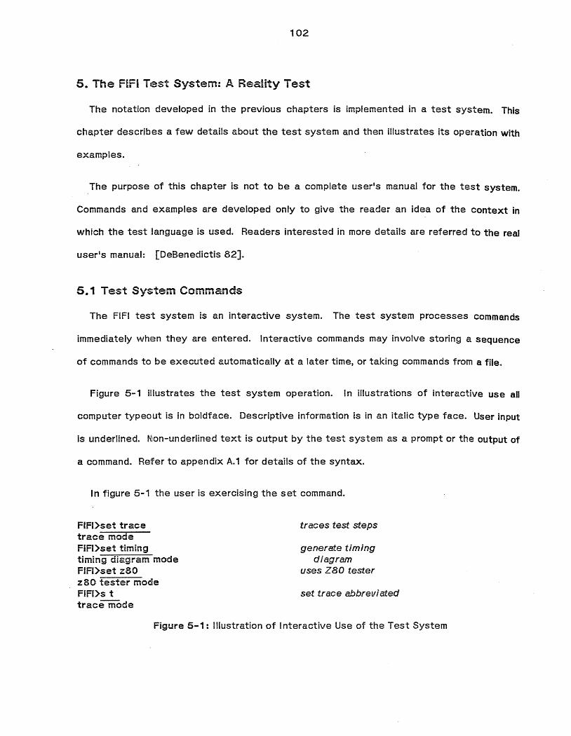
102
5. The FfFI Test System: A Reality Test
The notation developed in the previous chapters is implemented in a test system. This
chapter describes a few details about the test system and then illustrates its operation with
examples.
The purpose of this chapter is not to be a complete userls manual for the test system.
Commands and examples are developed only to give the reader an idea of the context in
which the test language is used. Readers interested in more details are referred to the real
userls manual: [DeBenedictis 82].
5.1 Test System Commands
The FIFI test system is an interactive system. The test system processes commands
immediately when they are entered. Interactive commands may involve storing a sequence
of commands to be executed automatically at a later time, or taking commands from a file.
Figure 5-1 illustrates the test system operation. In illustrations of interactive use all
computer typeout is in boldface. Descriptive information is in an italic type face. User input
is underlined. Nion-underlined text is output by the test system as a prompt or the output of
a command. Refer to appendix A.1 for details of the syntax.
In figure 5-1 the user is exercising the set command.
FIFI>set tracetrace modeFIFI>set timingtiming diagram modeFIFI>set z80z80 tester modeFIFI>s ttrace mode
traces test steps
generate timingdiagram
uses 280 tester
set trace abbreviated
Figure 5-1: Illustration of Interactive Use of the Test System

103
5.1.1 Loading Test Programs: Define Command
Test programs are loaded into the test system with the define command. The test system
maintains lists of the definable entities: procedures and ports. When a procedure or port
definition is processed, the input is checked for syntax only, semantic checking is done later.
Figure 5-2 illustrates a define command.
FIFI>define port clk 1;FIFI>define procedure frogFIFI> (loop i 1100 clk< 1;FIFI> clk<Oj)FIFI>endFIFI>--
new port named elkdefinitions
may be more thanone line in length
procedure frog
Figure 5-2: Examples of the Define Command
5.1.2 Executing Test Programs: Execute and Immediate Commands
The effect of executing a test program depends upon the mode. Each different kind of
tester will require different input from the test language system and may only implement
some of the features of the test language. There are also some modes that do not actually
operate on a device. The modes and their effects are described below:
trace mode In trace mode the port operations are printed when they are executed.
timing diagram mode In timing diagram mode the execution is assembled into its rectangularmatrix representation. When the command is finished, the rectangularmatrix is printed.
z80 tester mode In z80 tester mode commands are generated to drive the Z80 tester.It is assumed that the user is at a tester console and a chip isconnected to the tester.
The command to invoke a main test program is execute. The execute command takes one
argument that is the name of a defined procedure13.
13There is no distinction between a testing procedure and a main test program. A .maintest program is written as a test procedure, but it is never called by any other procedure.The user will invoke the main test program by its name. The test language is like the Cprogramming !anguage in this respect: a main program in C is a procedure with name 'main'.

104
The immediate command interprets, compiles, and executes a one line test language
command. The immediate command is used for interactive debugging of test programs.
Figure 5-3 shows an example of the execution commands. Refer to appendix A.1 for the
syntax of the execution commands.
FIFI>set timingtiming diagram modeFIFI>define port elk 1;FIFi>deffne procedure frogFIFI> (loop i 1 2 elk<1 ;FIFI> clk<O;)FiFi>endFfFI>execute frogelk
+-------+1<1 I1<0 I1<1 I
1<0 I+-------+FIFI>immediate (loop i 1 4 clk<i[O]);elk
+-------+1<0 II <1 I1<0 11<1 I+-------+FIFI)
timing diagram
new port named clkdefinitions
may be more thanone line in length
procedure frogwiggles elk 2 cycles
timing diagram
does same thing
timing diagram
Figure 5-3: Example of Execution Commands
5.1.3 Miscel!aneous Commands
A few other commands exist and are described below:
read
print port
print procedure
The read command takes input from a file rather than the terminal.\AJhen the file is complete control returns to the terminal.
If the name of a port is provided then the definition of the port isprinted, otherwise a listing of all defined ports is printed.
If the name of a procedure is provided then the definition of theprocedure is printed, otherwise a listing of all defined procedure isprinted.

quit Test system exits.
105
Figure 5-4 illustrates the commands described above by showing a terminal session.
@type testfiledefine port a 1 2 3jdefine port b 4 5 6;define port c 7 8 9;define procedure x a<1 ,b}2;c<3j end@fifiFIFi>read IItestfilell
FfFI>print portPorts:cbaFIFI>print port aport a 1 2 3;FIFI>p pr xprocedure xa<1,b>2;
c<3;end
FIFI>quit
will be read later
test program startedfilename in quoteslist of ports printed
port a printed
print proc. x abbr.
exit to monitor
Figure 5-4: Illustration of Miscellaneous Commands
5.2 Some Examples of the Test language
This section demonstrates examples and gives explanation of the test language. The
purpose is to illustrate some of the abilities of the language, and demonstrate some tricks
that may not be obvious initially.
5.2.1 Testtng the Adder in a zao Microprocessor
How to test an adder if the inputs to the adder are directly available is well known, see
section 1.1. It is much more difficult to test an adder if it is embedded inside a complex or
irregular device. One purpose of this demonstration is to show how the parts of the Z80

106
microprocessor that surround the adder can be stripped away. This will allow exercising the
adder as though it were directly accessible.
This demonstration also illustrates some of the abstractive nature of the test language.
In an abstract interpretation the Z80 processor has three basic cycles; instruction fetch,
read, and write. The instruction fetch has a different number of clock periods and different
timing from the read and write. The read and write are identical, however, except for the
direction of data flow during the cycle.
In this demonstration, the similarities of the read and write cycles are abstracted. There
is a single cycle, called a mcycle, that can perform either a read or write cycle depending
upon the type of the argument provided.
First the definitions of the pins. Only those pins relevant to the demonstration are
required. The first two pins, power and gnd, are not used by the test system, but instead
are present to remind the technician setting up the test fixture of manual connections that
must be made. (Also, these commands could be properly interpreted by a more sophisticated
tester.)
FIFI}define port power 11;FlFI}define port gnd 29;FIFI}define port: addr 5 4 3 2 1 40 39 38 37 36 35 34FIFI} 33 32 31 30;FIFI}define port: data 13 10 9 7 8 12 15 14;FIFI}define port elk 6;FIFI}define port reset 26;
The following is a procedure to reset the processor. It takes a var null due to an
oversight in the design of the language. In the language at present there is no way to
invoke a procedure without passing at least one argument.

107
FIFI)define procedure resetFIFI) var null;FIFI) reset<O;FIFI) (loop I 1 10 clk<1 jclk<Oj), reset<1;FIFI) (loop I 1 2 clk<1 ;clk<Oj), cik<1;FiFI>end
The ifetch procedure performs an instruction fetch cycle for the microprocessor. The
necessary parameter in an instruction fetch is the opcode that the machine will execute.
This procedure accepts this opcode as the parameter named opcode.
FIFI>define procedure ifetchFIFI> var opcode;FIFI) (loop I "i 4 clk<1 ;clk{Oj) +FIFI) (step 1: data{opcodej) +FIFI) (step 1: m1 }OJ) +FIFI) (step 5: m1)1 j) +FIFI) (step 6: m1 <~JUlLj) +FIFI> (step 8: data<NULLj)FIFI)end
step IV skips N stepsapply opcodem 1 should be lowm1 goes highm1 goes lowshut off data bus
either read or writeshut off data bus
The mcycle procedure performs both the read and write cycles for the microprocessor.
Although the read and write cycles generate different sequences of transitions on the mreq,
rd, and wr lines, these signals are not necessary to exercise the internal parts of the
processor. The direction of data transfer in this procedure is determined by the type of the
argument::!.:. The type of~may be force, feel, or interrogate.
FIFI)define procedure mcycleFIFI) var d;FIFI) (loop I 1 3 clk<1 jclk(Oj) +FfFI) (step 5: data=dj) +FIFI) (step 6: data<NULLj)FIFI)end
The following three procedures build macroinstructions upon the cycles ifetch and mcycle.
The macroinstructions are to load the accumulator, store the accumulator, and add to the
accumulator. Each of these instructions are two cycles. The first applies an opcode to the
processor, and the second reads or writes data.

108
The last operation performed in ea.ch procedure is to change the clk pin to 1. This puts
the processor into a static state. With the clk pin in the 0 condition, the internal ports of the
processor are subject to dynamic discharge and would change after about 15 seconds at
room temperature. This is undesirable in interactive use of the language wherein a 15
second delay is not uncommon.
F!FI>define procedure loadFIFI> var value;FIFI> (can ifetch opcode{16r3e;),FIFI> (call mcycle d<value;), elk<1;FIFI>end
FIFI>define procedure addFIFI> var value;FIFI> (cail ifetch opcode{16rc6;),FIFI> (cail mcycie d<valuej),clk<1;FIFf}end
FIFI>define procedure storeFIFI> var valu:e;FIFI> (caB ifetch opcode{16r02;),F1FI> (call meyele d=vatue;), 011<.< 1;FIFI}end
Id Q,nn instruction
add a,nn instruction
Id (bc),a instruction
The following procedure is a top level test program that is invoked by the command
execute entered interactively. The procedure will add two numbers, 23 and 1 and examine
the result. Since the result is examined with a feel operation, the user will receive no
response from the test instrument if the processor is working properly. Only if the value 24
is not sensed on the outputs will any response occur.
FIFI}define procedure tpFIFI) (cail reset nUII<O;),FIFI} (cail add value<"5 ;),FIFI>end
(call load value<23;),(call store vaiue)24;)
Figure 5-5 is a log of a terminal session using the file just discussed. The session uses
the tp procedure to load the accumulator with 24. The add and store procedures are then
invoked manually.

109
Demonstration Run of the FEFI System
@fifiFIFI>...etc...FIFI>execute tp~IFI>i (call store va.lue!;)24FIFI>i (can add value<12;)FIFi>i (call store valuel;)36FIFI>
previous inputexecutes but no print
Figure 5-5: Output From a Sample Run of the FIFI System
5.2.2 Testing Instruction Decoding in a zao Microprocessor
The instruction decoding logic in a Z80 microprocessor is very irregular sequential logic
designed without any testability in mind. In this example this logic is exercised in an attempt
to locate possible problems.
The strategy used in this example is to make the microprocessor execute each opcode
and to verify that the time required is correct. If there were a problem in the instruction
decoding or in the timing of memory or arithmetic cycles, this problem might cause an
instruction to become longer or shorter by some number of cicek cycles.
This is an example of testing art. It is expected that this testing strategy will be good at
locating a wide variety of problems, but there is no way of verifying this assertion. Because
the testing does not make use of any special design features that enhance testability (there
probably are none) the efficiency of the test is low. Since it is assumed that the instruction
decoding logic is combinational logic with 8 input wires, it should be testable in 256 steps.
This strategy requires one instruction execution, consisting of a number of steps, to test
each of the 256 combinations.

110
The first step is to determine the number of clock cycles required for each instruction to
execute. This information is available from the manufacturer. The execution time of
conditional jump instructions and two opcode instructions are dependent upon more than just
the opcode, and hence cannot be tested by this method. All other opcodes can be tested.
An excerpt of this table is shown below:
opcode00010203040506070809
mnemonicnopId bC,nnId @bc,ainc bcinc bdec bId b,nnricaex af,afadd hl,bc
number of cycles410764474411
The next step is to construct a testing procedure that applies a given opcode to the z80
and verifies that the number of cycles is correct. The procedure below performs this
function.
FIFI)define procedure instFIFI} var opcode cyc;FIFI> (caH ifetch opcode{opcode;),FIFI} (loop i 5 eyeFIFI> clk<1;FIFI> clk<Oj),FIFI> clk<1;FIFI}end
cyc is length of instruction
may execute 0 times
clock high to preventdynamic discharge
The procedure ifetch and mcycle have been previously described. The verification that an
instruction uses the proper number of cycles is performed by ifetch on the next instruction
fetch.
A test program to test the instruction lengths is shown below:

FIFI>define procedure lengthFIFI> (call reset nuH<Oj),FIFI> (call instFIFI> opcode(O,cyc(4;FlFI> opcode{1 ,cyc(1 0;FIFI> opcode(2,cyc<7;FIFI> opcode(3,cyc<6j)F~FI> opcocle(4,cyc{4;FIFI> opcoae{5,cyc(4;FIFI> opcode{6,cyc<7;FIFI> opcode<7,cyc<4;FiFI> opcode<S,cyc<4;)FIFI> opcode(9,cyc<11 ;)FIFI> opcode<O,cyc(4j)FIFI>end
The test program is invoked as follows:
FIFI>execute lengthFIFI>FIFI>
5.2.3 Reading the ROM of an 8041
111
reset processormultiple calls
separated bysemicolons
check last instruction
no [check f ailed]because it worked
The following is a very simple example illustrating use of the test system as a general
purpose interface between the world of programming notations and the world of electronics.
The problem addressed in this example is reading the ROM of a one chip factory programmed
microprocessor, the Intel 8041 [Intel 80].
The Intel databook describes a method of reading the ROM that involves about a dozen
functions which must be performed for each byte in the ROM. One method of performing this
task would be to build a special purpose machine that would perform these dozen functions
and send the results to a computer. Such a special purpose machine would involve an
expenditure of time that would not be justified except in extremely high volume applications.
In this example the test system is set up to perform this task. The total effort involved
was to write the program shown, and to interface the chip to the tester.

power connectionpower connectionspecial +12v supplycrystalcrystal
112
Interfacing, in this case, involved some unusual tasks. To read the ROM it is necessary to
apply +12 volts to a certain pin. The solution to this was to disconnect that pin from the
tester and connect it to a +12 volt power supply. Another problem is that the specifications
indicate the processor should have a 3 MHz clock running during the process. Since this
implementation of the test instrument was not capable of that speed, the clock pins were
removed from the tester and a crystal was connected.
The first section is the pin definitions. The first five are reminders for setup. gnd and vee
are connected to standard power supplies. v12pullup is connected ,to +12 volts through the
specified pullup resistor. phi1 and phi2 are connected to a crystal.-- --FIFI>define port gnd 20;FIFI>define port vee 40;FIFI>define port v12puHup 7;FIFI>aefine port phi1 2;FIFI>define port phi2 3;FIFI>define port ea 7;FIFI>define port abus 22 21 19 18 17 16 15 14 13 12;FIFI>define port dbus 19 18 17 16 15 14 13 12;FIFI>define port reset 4;FIFI>define port to 1;FIFI>define port t1 39;FIFI>define port cs 6;FIFI>define port aO S;
The following procedure reads from ROM location addr and performs the function specified
by the type of data.
FIFI>define procedure mreadFIFI> var addr data;FIFi> reset<O;t to<O,cs<1 ,aO<O;FIFI> abus<addr;FIFI> reset<1;JtO<1;FIFI> abus<NULL;FIFI> dbus=dats;FIFI> reset<O;f to<O;FIFI>end
The main program procedure does the read function for each location in ROM. It specifies

113
the interrogate function that prints the answer on the terminal. The output of the test
program can be logged and the contents of the ROM can be extracted.
FIFI>define procedure xFIFI> (can mreadFIFI> (loop I 0 1023 addr<l,data!;»FIFI>end

114
6. The Design of Test Instruments
There are different types of testing with different requirements on the test instrument
and test software. It would be desirable to have a series of compatible testers available,
each optimized to a particular phase of the testing process.
For example, the process of characterizing a device and developing a production test set
is a slow process with much human interaction. There is no need for the test instrument be
extremely fast or accurate, so it would be expected that the test instrument for this phase
be Enexpensive, but what about the computer behind it? On the other hand, production
testing must be performed with high speed and accuracy. Since the test instrument for this
application is efficiently utilized, its cost can be higher. For such a set of testers to be
useful, however, it is necessary to have assurance that a test developed on one tester will
be valid when executed on another.
We will describe a general design strategy for testers. By implementing only some of the
parts described, specialized testers can be constructed. By implementing the parts in
different architectures and technologies, the speed and cost of the test instrument can be
varied. Any such tester will be able to execute the same test specification and achieve
valid results.
6.1 Constrained Tests and Tester Design
The test language developed previously has supported only non-adaptive tests sequences.
A non-adaptive test can be executed by a pipelined tester. Such a test would consist of
the stimulus and expected response of the chip. All comparisons can be performed in the
test head and would effect only the state of a fault flag.
An adaptive test requires that the output of the chip be fed back to the test pattern

115
generator. During the time that the test pattern generator is interpreting the response of
the chip the remainder of the tester would be idle. If the tester were pipelined, each value
returned from the chip would require that the pipeline be flushed.
The proposed manner of constructing test systems includes both highly pipelined hardware
and feedback from the chip. In production testing feedback from the chip would not be
required, and the test would be executed at pipelined speeds. Other uses of the tester,
such as exploratory testing uses, require information returned from the chip be displayed. In
non-production testing high speed is less important, and less efficient use of the pipeline
would be tolerable.
6.2 High Performance Test Instruments
In practice, the number of vectors in a high fault coverage test for a large integrated
circuit may be astronomical. Conventional testers, where the entire test must be
instantiated in storage, must be provided with an huge amount of storage. Exploitation of
the structure of the test language can yield a tester design where storage requirements are
minimized.
6.2.1 Conventional Tester Design
The average general-purpose IC tester consists of two parts: a Von-Neuman type
computer and a high speed test vector buffer. The computer is used for making low-speed
measurements (DC parametric testing) and manipulating the high speed vector buffer. The
high speed vector buffer is capable of storing from 500-500,000 test vectors for application
at 1-100 MHz.
In the testing of a chip the computer will perform several thousand parametric tests at a
rate of about 1 per millisecond. The reason for the slow speed of 1 mS per test is twofold:

116
the computer is slow, and parametric tests require accurate analog measurements that take
a long time to perform.
The test vector buffer is totally under the control of the computer. The computer loads
test vectors. from secondary storage (disk.) and instructs the test vector buffer to dump its
contents to the device under test. Usually the test vectors are dumped at a fixed rate, but
possibly with a number of clock phases. In the event that a test is larger than the size of
the test vector buffer, the test must be broken into smaller sections and executed
sequentially.
An additional duty of the computer is to configure the test head. The physical conductors
leading to the device under test are usually (although not always) connected to the tester
electronics though a crossbar switCh, allowing all pins to be the same. A tester will have a
supply of drivers of different types: a clock, inputs, outputs, input/output combinations, and
special measurement units. Setup consists of allocating drivers to the pins of the chip.
Sometimes there will not be as many drivers of a particUlar type on the tester as required by
the chip. In this case the solution is to buy a bigger tester.
The conventional design of testers has the advantage of extreme simplicity, but is quite
irregular to program.
6.2.2 Areas for Improvement
Although a test could reasonably consist of a billion test vectors, there is a great deal of
redundancy in the test vectors that can be exploited. A memory test, for example, can be
expressed in less than one page with the test language, but expands to millions of test
vectors.
There are two strategies for the efficient storage and generation of test vectors:

117
1. Elimination of redundant information in the test vectors by either bitcompression of the instantiated test vectors, or by storing the test vectorsbefore they are fully instantiated.
2. Algorithmic generation of test vectors. Simple algorithms such as generatingcount and shift sequences, and substitution of small amounts of data intootherwise static groups of test vectors are sufficient.
6.2.3 Efficient Use of Test Vector Storage
The great majority of the test vectors in a large test consist of repetitions of a few
vectors many times. Some examples are: groups of vectors that cause an instruction to be
executed in a microprocessor, or an access sequence for an ALU in a microprocessor, or a
memory cycle. In each of these cases the test vectors are applied many times and changed
in only very minor ways each time. The vectors that execute an instruction are different in
the opcode and data each time, but are otherwise the same. Similarly for an access
sequence. Memory accesses are different in address and data, but have identical timing.
An (intermediate) test language can be made to represent tests compacted in this way.
Such a test language would consist of statements of the following types:
Fully Instantiated Test VectorsFully instantiated test vectors to be applied many times.
Execution InstructionsInstructions for the test vector buffer to apply groups of test vectorsto the device under test. This statement would carry two test vectornumbers, like apply vectors 23 through 87.
Change Instructions Instructions to alter small portions of the test vector buffer memory.This statement would have information to store, a vector number, and aposition in the vector, such as: store 03 into vector number 23,positions 15,9, 12,6,3, 11, 13, 14.
A tester to execute this intermediate form would have the appearance of figure 6-1.
Figure 6-1 does not show the source of test vect?rs, they may come from a computer or
from more advanced test generators. There are three new functions in the hardware:
1. The test command interpreter. This device split3 the stream of testcommands into three streams: one to the sequencer, one to the test vectorbuffer, and one to the change unit.

118
+-------------------+I test 1
+--------->+ output II I sequencer II +---------+---------+I II VI +---------+---------+
+-----------+ I I I +--------+I test +--+ I test +<--->+ pin I
->+ command +------------>+ vector I I driversllinterpreter+--+ I storage I +--------++-----------+ I +---------+---------+
I ~
I II +---------+---------+I I change I+--------->+ unit I
I I+-------------------+
Figure 6-1: Buffered Test Generation Unit
2. A test vector sequencer. The sequencer generates vector addresses fortransfers from the test vector storage to the pin electronics.
3. The change unit. The change unit alters small portions of the test vectorbuffer.
6.2.4 Interface of the Tester Model to the Test Language
The application of the test language to the model of a tester just described is
straightforward.. The lowest level testing routines, those that do not call any others, are
compiled into groups of test vectors. These test vectors are then loaded directly into the
vector storage. The remainder of the test specification consists of invocations of the low
level testing routines and arguments. The test specification would be stored as a series of
change instructions and execution instructions.
The effectiveness of this strategy would depend upon the statistics of the test vectors.
In some cases, such as microprocessor testing, the amount of change information would be
very small in relation to the total test vectors. In a memory test, however, the address

119
would have to be changed every few vectors, resulting in only a modest information
reduction.
6.2.5 Further Refinements in Tester Design
Several additional refinements can be made in the design of testers to optimize their
design to the test language. The most significant improvement can be obtained by
considering the high speed execution of low level testing procedures.
In most cases a low level testing procedure can be compiled into a static set of test
vectors and a number of translations. The translations specify operations to be performed on
the arguments of the procedure and a location in the vectors :to store the result.
Figure 6-2 illustrates a low level testing procedure and its compiled form. The compiled
form consists of a rectangular matrix of test vectors with the static portion of the
procedures, and a translation that specifies how the argument is processed to generate the
complete testing procedure.
procedure rectangular matrix translationclk control data
procedure ptos +----------------+var data; I B 23 I
(loop i 1 4 I 1 85 X<)-------+clk<B,control<23,data<NULL; I B 23 I Iclk<1,control<85,data=data[i]; I 1 85 X<)-----+ I
I B 23 I I Iend I 1 85 X<)---+ I I
I B 23 I I I II 1 85 X<) -+ I I I+----------------+ I I I I
+-+-+-+-+I I I I I+-+-+-+-+
data
Figure 6-2: A Testing Routine and its Instantiation

120
It is not always possible to compile a testing procedure into a rectangular matrix and
translations. If the procedure uses arguments as bounds in loops, the number of vectors in
the rectangular matrix may vary. The software that generates the translation must verify
that the procedure can be compiled.
6.2.6 Analogy' of Tester Design to the DesEgn of Computers
There are some parallels between the strategy devised here for the design of testers to
the design of mainframe computers.
6.2.6.1 Virtual Memory vs the Test Vector Buffer
In the early days computer programs were very small, say averaging 10,000 bytes,
because software technology was not very advanced. In those days, memory was
expensive and hence computers were designed with no more than was necessary, say
65,000 bytes. In the early days, however, programs were small enough to fit into the
memory of computers.
As time passed, computer programs became larger and memory became cheaper. As
memory became cheaper, existing computers were supplied with more and more memory, up
to the limit for vu'hich they were designed, 65,000 bytes. Programs similarly grew, up to the
memory capacity of the machines, 65,000 bytes. At this point the the computers had run out
of memory, and lather techniques would have to be used.
One solution to this problem was to use overlays. Overlays solve the addressing problem
by splitting a program into sections that will fit in the machine. Partitioning a program in this
way was rather difficult, and hence overlays were never very popular.
Another solution was virtual memory. The architecture of new computers was made to
support an astronomical amount of memory, 4 bHlion bytes. Of the 4 billion bytes, only a small

121
portion could be used, several million bytes; the remainder was reserved for future
expansion. Providing memory that would only be used a decade in the future would prevent
all the programs written for th e present machine from becoming obsolete.
Some of- this story applies to testers. We are still in the early days where testers have
very small buffer memories. Unfortunately, the needs of test software exceed the vector
memory of most testers, and the industry is dealing with overlays of test vectors. The near
absence of high level test software is evidence that the 'overlays' are not working well.
What is needed to boost testing to its next plateau is a freedom from the constraints of the
tester hardware.
6.3 Requirements for Test Instruments
There are some tradeoffs between tester designs. These are summarized below.
Speed and Cost Production testers must be extremely fast, but a higher cost istolerable. Interactive testers must be inexpensive, but reducedperformance and accuracy are acceptable.
Flexibility and Speed Production testers do not require flexibility. A go/no-go indication issufficient. Exploratory testers must be as flexible as their operator'smind.
A successful test system should address as many of these issues as possible.
Unfortunately, some of these requirements conflict.
Test language systems would be devised to communicate with a tester in a standard form.
Differences in testers would be handled by a set of parameters describing such
characteristics as the size of the test vector storage area, the complexity of translations,
speed, etc. With appropriate choice of parameters and the standard communication protocol,
a tester of any size could be interfaced to a single test language system.
An extremely small and inexpensive test system could be constructed by interpreting the

122
test instruction set with a microprocessor. The size of the test vector storage area could be
as small as one vector, and the maximum number of translations could be zero. This would
force the test language system to send all vectors to the tester. Timing commands could be
ignored.
A large tester, on the other hand, could have generous amounts of all the resources
described above.

123
7. Conclusions
We have described a complete test system. The heart of the system is the test
language. The test language was shown to be capable of representing tests for a number of
conventional. design disciplines in a natural way. The test language is also easily and
efficiently implemented, as was demonstrated by the FIFI test system.
A general philosophy for designing systems in a manner that aids testability was
presented. The method uses the test language as a manner of formally specifying the
testability attributes of parts of a design. A method was then proposed for composing these
parts into systems and guaranteeing testability. The result is somewhat more general than a
conventional design-far-testability strategy; a strategy for designing design-for-testability
strategies was proposed.
The test system described has been demonstrated in a number of ways. We have
implemented an interactive test system. Students at Caltech have used the test system
interactively to manually characterize some of their IC design projects. We have
demonstrated the abstractive abilities of the test language. The translation of a list of
primitive tests for combinational logic into a complete test specification for the logic when in
a microprocessor has been done, and was illustrated here.
Several other observations can be made about the test system and its future: a careful
examination of real tests indicates that test specifications actually do follow the structured
approach proposed here. A careful look is necessary, however, because there has been no
tool that can represent the design abstractions in an appropriate way, and hence real tests
do not look structured!
For example, Motorola in the 68000 microprocessor employed a structure similar to that

124
depicted in figure 3-10. Testability strategies that describe general classes of devices by
making parameterized libraries of testing routines that can be assembled automatically for
specific devices fits the flavor of bristle blocks [Johannsen 79] nicely.

125
A. Syntax of the Test language
This appendix specifies the syntax of the test language and the FIFI test system. The
syntax will be described as a production grammar as defined in [Aho 72], page 85.
In the notation that follows non terminal symbols will be represented in italic type, i.e.
nonterminaJ.
Terminal symbols fall into several types: keywords, identifiers, punctuation, numbers,
texts, newlines, and endfiletokens. In all cases the terminals will be in boldface type. The
different types of terminals are described as follows:
word
keyword
identifier
punctuation
number
newline
text
endfiletoken
A word is a sequence of letters or numbers, starting with a letter, andterminating with a character that is not a letter or number. In thesemantic analysis of words, upper and lower case character aretreated as different.
A keyword is a word from a predefined set known as the keywords.Keywords are represented as IIXXXIl
• The set of keywords includes allkeywords of the form "XXXII in this syntax representation.
An identifier is a word that is not a keyword. Identifiers arerepresented as ident.
A punctuation is a single character terminal. The character may be aprinting character but may not be a letter or number. A character isrepresented as '#'.A number is a representation of a numerical value. One form of anumber is a string of digits. The numerical value of the number is itscommon numerical representation in base 10. A second form of anumber is a string of digits, followed by Ir', followed by a string ofextended digits. The second form allows numbers to be represented inan arbitrary radix. The first string of digits specifies the radix, and thestring of extended digits is the number in the specified radix. Anextended digit is a digit with value 0 through the radix-1 where theletters a-z and A-Z represent values 10-35. Some examples ofnumbers are: 10 value 10, 16rff value 255.
Invoked by the user terminating the line. Represented by newline.
A string of characters surrounded by double quotes. Texts may not bemore than one line in length; a newline will take the place of thesecond quote. Represented as text.
The indication from the operating system that no more input will beavailable from a file. Represented as endfHetoken.
Productions are represented in the following form:

loopfcn
126
-} 1(1 IIloopli ident expr expr tvexpr 1)1
The sentence symbol is command.
A. 1 User Commands
command
command
command
command
command
command
command
command
command
command
command
command
command
command
command
command
-} Udefine" matdecl newline
-} IIdefine" pindecl newline
-} IIsetli " z80" newline
-} "setll litiming" newline
-} "setll "trace" newline
-} "setll IIdebug" newline
-} "read" ident newline
-} "readll text newline
-) UimmediateU tvexpr newline
-} Uquitll newline
-) endfiletoken
-} lIexecute" ident newline
-) "print" "procedure" ident newline
-} IIprint" IIprocedure" newline
-) "print" IIport" ident newline
-) "print" "port" newline
A.2 Procedure Declarations
matdecl
matdecl
varUst
varlist
varsublist
varsublist
-) "procedurell ident varUst tvexpr lIendll
-) "procedure" ident tvexpr Uend"
-} IIvar" varsublist 1;1 varlist
-} " Varn varsublist 1;1
-} ident varsublist
-} ident

127
A.3 Port Declarations
pindecl
pinlist
pinlist
-) "portll ident pin/ist 1;1
-} number pinlist
-) number
A.4 Typed Value Expressions
Typed value expressions are formed from the operators below and exprs in a normal
expression syntax. The mixture of the exprs, which are expressions themselves, into a
higher level expression syntax is somewhat unusual.
OPERATORS
lowestprecedence
highestprecedence
operator+
,( )
unaru/binarybinarybinary
postfix unarybinary
nameplussemisemicomma
parenthesis
tvexpr
tvplus
tvplus
tvsemi
tvsemi
tvsemi
tvsemi
tvcomma
tvcomma
tvparen
tvparen
tvparen
tvparen
tvparen
tvasgn
tvasgn
tvasgn
tvasgn
tvasgn
-) tvplus
-} tvsemi
-) tvplus 1+1 tvsemi
-} tvcomma
-} tvsemi 1+1 tvcomma
_) 1;1 tvsemi
-} tvsemi 1;1
-) tvparen
-} tvcomma 1;1 tvparen
-) 1(1 tvexpr 1)1
-} tvasgn
-) 1(1 IIloopll ident expr expr tvexpr 1)1
-} 1(1 IIstepll expr 1:1 tvexpr 1)1
-) 1(1 II caUI: ident tvexpr 1)1
-} ident I{I expr
-) ident I}I expr
-)ident 1:l expr
_) ident Ip
-} ident I{I IINULLII expr

128
A.5 Expressions
In summary, expressions are formed of the operators below and idents or numbers in a
normal expression syntax.
OPERATORS
lowestbindingpriority
highestbindingpriority
operatorI1-&«»+
[e]( )
unary/binarybinarybinarybinarybinarybinarybinarybinary
postfix unary
nameorxorand
sh i ft Ieftshift right
plusmultiply
bit subscr ip t see noteparenthesis
expr
expr
typxor
typxor
typand
typand
typleft
typleft
typright
typright
typlus
typlus
typmul
typmul
typsubscr
typsubscr
typsubscr
typatm
typatm
(Note: the e in bit subscripting is either a typevalue expression or two typed value expressionsseparated by 11:11 and represents bit subscripting.)
-}typxor
-} expr III typxor
-} typand
-} typxor ItI typand
-} typleft
-} typand 1&1 typleft
-} typright
-} typleft 1<1 1<1 typright
-} typlus
-} typright I}I I}I typlus
-} typmul
-} typlus 1+1 typmul
-} typsubscr
-} typmu/ iltl typsubscr
-) typatm
-} typatm Ip expr 1]1
-} typatm Ip expr 1:1 expr 1]1
-} number
-} ident

typatm
129

[Agrawal 75]
[Aho 72]
[Bouricius 71]
[Bryant 81]
[Bryant 82]
[DeBenedictis 79]
[DeBenedictis 80]
[DeBenedictis 82]
130
References
Agrawal, P., and Agrawal, V.Probabilistic Analysis of Random Test Generation Method for Irredundant
Combinational Logic Networks.IEEE Transactions on Computers C-24:695-700, July, 1975.
Aho, A., and Ullman, J.Prentice Hall Series in Automatic Computing.: The Theory of Parsing,
Translation, and Compiling.Prentice Hall, 1972.
Bouricius, W., Hsieh, E., Putzolu, G., Roth, P., Schneider, P., and Tan, C.Algorithms for Detection of Faults in Logic Circufts.IEEE TrBs'1sactions on Computers C-20: 1258-1263, November, 1971.
Bryant, R.A SI'.litch-Level Simulation Model for Integrated Logic Circuits.Technical Report MIT/LCS/TR-259, Massachusetts Institute of
Technology, March, 1981.
MOSS/M II: A Switch-Level Simulator for MOS LSI, User's ManualCaltech Computer Science Department, 1982.
DeBenedictis, E.Multilevel Simulator.Master's thesis, Carnegie-Mellon University, May, 1979.
DeBenedictis, E.A Preliminary Report of the Caltech ARPA Tester Project.Technical Report 4061, Caltech Computer Science Department, April,
1980.
DeBenedictis, E.FIFI Test System User's Manual.Technical Report, Caltech, 1982.

[Eichelberger 77]
[Fairchild 80]
[Hayes 74]
[Ibarra 75]
[IBM 80]
[IEEE 80]
[Intel 80]
[Johannsen 79]
[Konemann 80]
[Mead 80]
131
Eichelberger, E., and Williams, T.A Logic Design System for VLSI Testability.In Proceedings of the 14th Design Automation Conference, pages
462-468. IEEE/ACM, 1977.
Series 20 FACTOR Programming Language Reference MenuaJFairchild Test Systems Group, Customer Services, MIS 36-07/57, 1725
Technology Drive, San Jose, California 95110, 1980.
Hayes, J.On Modifying Logic Networks to Improve their Diagnosablility.IEEE Transactions on Computers C-23:56-62, January, 1974.
Ibarra, 0., and Sahni, S.Polynomial Complete Detection Problems.IEEE Transactions on Computers C-24:242-249, March, 1975.
An IBM representative.Miscellaneous discussion.
IEEE Guide to the Use of AtlasInstitute of Electrical and Electronics Engineers, Inc, 1980.
Component Data CatalogIntel Corporation, Literature Department, 3065 Bowers Avenue, Santa
Clara, CA 95051, 1980.
Johannsen, D.Bristle Blocks: A Silicon Compiler.In 16th Design Automation Conference. IEEEIACM, 1979.
Konemann, B., Mucha, J., Zwiehoff, G.Built-In Test for Complex Digital Integrated Circuits.IEEE Journal of Solid State Circuits SC-15:315-319, June, 1980.
Mead, C. and Conway, L.Addison-Wesley Series in Computer Science.: Introduction To VLSI
Systems.Addison-Wesley, 1980.

[Nagel 73]
[Organick 73]
[Pereira 78]
[RCA 76]
[Rowson 80]
[Savir 80]
[Seitz 71]
.[Snoulten 81]
132
Nagel, L., and Pederson, D.Simulation Program with Integrated Circuit Emphasis (SPICE).In Proceedings of the 16th Midwest Symposium on Circuit Theory. IEEE,
1973.
Organick, E.ACM Monograph Series.: Computer System Organization: The
85700/86700 Series.Academic Press, 1973.
Pereira, L., Pereira, F., and Warren, D.User's Guide to DECsystem-1 0 Prolog1978.Documentation file on Caltech DEC-20.
RCA Integrated CircuitsRCA, RCA Solid State, Box 3200, Somerville, N.J. 08876, 1976.Pages 692-698.
Rowson, J.Understanding Hierarchical Design.PhD thesis, Caltech, April, 1980.
Savir, J.Syndrome-Testable Design of Combinational Circuits.IEEE Transactions on Computers C-29:442-451, June, 1980.Corrections published in November issue. .
Seitz, C.An Approach to Designing Checking Experiments Based on a Dynamic
Model.In Kohavi, Z., Paz, A., editor, Theory of Machines and Computations, pages
341-349. Academic Press, 1971 .
Snoulten, B., and Peacock, J.ANGEL - Algorithmic Pattern Generatio:l System.In Proceedings of the 1981 International Test Conference, pages
484-488. IEEE, 1981.

[Stanford 81]
[TI80]
[Timoe 81]
[Young 76]
133
Newkirk, J., Mathews, R., Watson, I.Testing Chips using ICTEST Version 1.Technical Report VLSI 020281, Stanford Information Systems Laboratory,
November, 1981.
The TTL Data BookTexas Instruments, Marketing Information Services, P. O. Box 5012, MS
308, Dallas, Texas 75222, 1980.Page 7-53.
Timoc, C.Lunch-bunch presentation, fall 1981.
Young, T., and Dutton, R.MINI-rVlS/NC: A Minicomputer Simulator for MOS Circuits with Modular
Bui/t-in Mode/.Technical Report 5013-1, Stanford Electronics Laboratory, 1976.

Index
Action 24
Buffer test generator 1 7
Call control clause 40Comma 34,36Composition design 92Concatenation, design by 93Controllability 63
Dynamic interpretation 31
Elements 31Execution 34
Fault model 63Feel 23Force 23
Interrogate 23
Level of structure 69Loop control clause 35,37
Matching of actions 75Matrix expression 37Minimum step time 44
Non-adaptive test 114Non-adaptive tests 29
Observability 63Ordered pair 22
Phases of a test step 34Plus 35,36Port 24PortIs state 34Primitive tests 63
Recursive design 93
Semicolon 34, 36Semicolon special case 37Sequential test generation unit 1 7Static interpretation 31
134

Step control clause 37Step timeout 45
Tagged data architecture 23Test vector 34Test matrix 28, 31, 33, 34Test step 28Test vector . 16, 28Translations 11 9Tr~-state 23Type part 22Typed value 22, 33Typed value assignment 24Typed value expression 24
Undefined 23
Value part 22Var 40
Wait 23
135