Techniques for Increasing Security and Reliability of IP ... · grow rapidly. First, only basic...
325
Techniques for Increasing Security and Reliability of IP Cores Embedded in FPGA and ASIC Designs Der Technischen Fakult¨ at der Universit ¨ at Erlangen-N ¨ urnberg zur Erlangung des Grades DOKTOR-INGENIEUR vorgelegt von Daniel Michael Ziener Erlangen 2010
Transcript of Techniques for Increasing Security and Reliability of IP ... · grow rapidly. First, only basic...

Techniques for IncreasingSecurity and Reliability of IP
Cores Embedded in FPGA andASIC Designs
Der Technischen Fakultat derUniversitat Erlangen-Nurnberg
zur Erlangung des Grades
D O K T O R - I N G E N I E U R
vorgelegt von
Daniel Michael Ziener
Erlangen 2010

Als Dissertation genehmigt von der TechnischenFakultat der Universitat Erlangen-Nurnberg
Tag der Einreichung: . . . . . . . . . . . . . . . . . . . . . . . . . . . . 02. Juni 2010Tag der Promotion: . . . . . . . . . . . . . . . . . . . . . . . . . . . . . . . 27. Juli 2010Dekan: . . . . . . . . . . . . . . . . . . . . . . . . Prof. Dr.-Ing. Reinhard GermanBerichterstatter: . . . . . . . . . . . . . . . . . . . . Prof. Dr.-Ing. Jurgen Teich
. . . . . . . Prof. Dr. sc.techn. Andreas Herkersdorf

Acknowledgments
I would like to express my sincere gratitude to my advisor, Professor Jurgen Teich,for his guidance, and encouragement throughout this work. His scientific, technical,and editorial advice was essential for my work as an academic researcher. I wouldalso thank Professor Andreas Herkersdorf for the fruitful cooperation with him andhis chair and for agreeing to be the co-examiner of this work. My thanks also go to allmy colleagues for the discussions of my research work, especially Marcus Bednara,for the numerous scientific and editorial advises, and Moritz Schmid for his criticalreview of this thesis and his fruitful feedback and discussion. Finally, I would liketo thank my family and friends for their support and encouragement during the pastyears.
Daniel ZienerErlangen, May 2010
iii

iv

Contents
1 Introduction 11.1 Motivation . . . . . . . . . . . . . . . . . . . . . . . . . . . . . . . 11.2 Definitions . . . . . . . . . . . . . . . . . . . . . . . . . . . . . . . 13
1.2.1 Dependability and its Attributes . . . . . . . . . . . . . . . 131.2.2 Fault, Error, Failure . . . . . . . . . . . . . . . . . . . . . . 161.2.3 Fault and Error Categorization . . . . . . . . . . . . . . . . 171.2.4 Means to Attain Dependability . . . . . . . . . . . . . . . . 181.2.5 Security Flaws and Attacks . . . . . . . . . . . . . . . . . . 201.2.6 Overhead . . . . . . . . . . . . . . . . . . . . . . . . . . . 221.2.7 IP Cores and Design Flow . . . . . . . . . . . . . . . . . . 23
1.3 Faults in Embedded Systems . . . . . . . . . . . . . . . . . . . . . 251.3.1 Degeneration Faults . . . . . . . . . . . . . . . . . . . . . 251.3.2 Manufacturing Faults . . . . . . . . . . . . . . . . . . . . . 261.3.3 Design Faults . . . . . . . . . . . . . . . . . . . . . . . . . 271.3.4 Single Event Effects . . . . . . . . . . . . . . . . . . . . . 27
1.4 Attacks on Embedded Systems . . . . . . . . . . . . . . . . . . . . 291.4.1 Code Injection Attacks . . . . . . . . . . . . . . . . . . . . 311.4.2 Invasive Physical Attacks . . . . . . . . . . . . . . . . . . . 331.4.3 Non-Invasive Logical Attacks . . . . . . . . . . . . . . . . 351.4.4 Non-Invasive Physical Attacks . . . . . . . . . . . . . . . . 35
1.5 Contributions . . . . . . . . . . . . . . . . . . . . . . . . . . . . . 371.5.1 Overview of the Thesis . . . . . . . . . . . . . . . . . . . . 40
2 Related Work 432.1 Security: IP Protection . . . . . . . . . . . . . . . . . . . . . . . . 43
2.1.1 Encryption of IP Cores . . . . . . . . . . . . . . . . . . . . 462.1.2 Additive Watermarking of IP Cores . . . . . . . . . . . . . 482.1.3 Constraint-Based Watermarking of IP Cores . . . . . . . . . 512.1.4 Other Approaches . . . . . . . . . . . . . . . . . . . . . . 55
2.2 Security: Defenses Against Code Injection Attacks . . . . . . . . . 562.2.1 Methods using an Additional Return Stack . . . . . . . . . 572.2.2 Methods using Address Obfuscation and Software Encryption 57
v

Contents
2.2.3 Safe Languages . . . . . . . . . . . . . . . . . . . . . . . . 582.2.4 Code Analyzers . . . . . . . . . . . . . . . . . . . . . . . . 592.2.5 Anomaly Detection . . . . . . . . . . . . . . . . . . . . . . 602.2.6 Compiler, Library, and Operating System Support . . . . . . 61
2.3 Reliability: Measures against Faults and Errors . . . . . . . . . . . 642.3.1 Hardware Redundancy Methods . . . . . . . . . . . . . . . 652.3.2 Time Redundancy Methods . . . . . . . . . . . . . . . . . 662.3.3 Information Redundancy Methods . . . . . . . . . . . . . . 692.3.4 Prevention and Detection of Single Event Effects . . . . . . 73
2.4 Reliability and Security: Control Flow Checking . . . . . . . . . . 742.4.1 Software-Based Methods . . . . . . . . . . . . . . . . . . . 742.4.2 Methods using Watchdog Processors . . . . . . . . . . . . . 76
2.5 Summary . . . . . . . . . . . . . . . . . . . . . . . . . . . . . . . 82
3 IP Core Watermarking and Identification 833.1 Introduction . . . . . . . . . . . . . . . . . . . . . . . . . . . . . . 833.2 Theoretical Watermark Model . . . . . . . . . . . . . . . . . . . . 87
3.2.1 General Watermark Model . . . . . . . . . . . . . . . . . . 873.2.2 IP Core Watermark Model . . . . . . . . . . . . . . . . . . 923.2.3 IP Core Identification Model . . . . . . . . . . . . . . . . . 97
3.3 Bitfile Watermarking and Identification . . . . . . . . . . . . . . . 983.3.1 Lookup Table Content Extraction . . . . . . . . . . . . . . 993.3.2 Identification of Netlist Cores by Analysis of LUT Contents 1023.3.3 Identification of HDL Cores by Analysis of LUT Contents . 1093.3.4 Watermarks in LUTs for Bitfile Cores . . . . . . . . . . . . 1123.3.5 Watermarks in Functional LUTs for Netlist Cores . . . . . . 115
3.4 Power Watermarking . . . . . . . . . . . . . . . . . . . . . . . . . 1223.4.1 Verification over Power Consumption . . . . . . . . . . . . 1223.4.2 Communication Channel . . . . . . . . . . . . . . . . . . . 1253.4.3 Basic Method . . . . . . . . . . . . . . . . . . . . . . . . . 1323.4.4 Enhanced Robustness Encoding Method . . . . . . . . . . . 1403.4.5 BPSK Detection Method . . . . . . . . . . . . . . . . . . . 1423.4.6 Correlative Detection Methods . . . . . . . . . . . . . . . . 1463.4.7 Multiplexing Methods . . . . . . . . . . . . . . . . . . . . 149
3.5 Experimental Results . . . . . . . . . . . . . . . . . . . . . . . . . 1553.5.1 Identification of Netlist Cores by Analysis of LUT Contents 1553.5.2 Identification of HDL Cores by Analysis of LUT Contents . 1563.5.3 Watermarks in LUTs for Bitfile Cores . . . . . . . . . . . . 1593.5.4 Watermarks in Functional LUTs for Netlist Cores . . . . . . 1603.5.5 Power Watermarking . . . . . . . . . . . . . . . . . . . . . 163
3.6 Summary . . . . . . . . . . . . . . . . . . . . . . . . . . . . . . . 176
vi

Contents
4 Control Flow Checking 1794.1 Introduction and Scope . . . . . . . . . . . . . . . . . . . . . . . . 179
4.1.1 AIS Project Overview . . . . . . . . . . . . . . . . . . . . 1804.1.2 AIS Work Packages Overview . . . . . . . . . . . . . . . . 181
4.2 Fault Injection . . . . . . . . . . . . . . . . . . . . . . . . . . . . . 1834.2.1 Intentional Fault Injection . . . . . . . . . . . . . . . . . . 1844.2.2 Random Fault Injection . . . . . . . . . . . . . . . . . . . . 185
4.3 Methods for Control Flow Checking . . . . . . . . . . . . . . . . . 1864.3.1 Branches and Jumps . . . . . . . . . . . . . . . . . . . . . 1864.3.2 Methods for Checking Direct Jumps/Branches . . . . . . . 1874.3.3 Methods for Checking Indirect Jumps/Branches . . . . . . . 1974.3.4 Methods for Handling a Corrupt Control Flow . . . . . . . 2004.3.5 IP Core Control Flow Checking . . . . . . . . . . . . . . . 201
4.4 Architectures for Control Flow Checking . . . . . . . . . . . . . . 2034.4.1 Handling Direct Jumps and Branches . . . . . . . . . . . . 2034.4.2 Handling Indirect Jumps and Branches . . . . . . . . . . . 2074.4.3 Handling Interrupts and Traps . . . . . . . . . . . . . . . . 2104.4.4 Checking Conditional Branches . . . . . . . . . . . . . . . 2124.4.5 Instruction Integrity Checker . . . . . . . . . . . . . . . . . 2134.4.6 Repairing a Corrupt Control Flow by Re-Execution . . . . . 2154.4.7 Bus Interface . . . . . . . . . . . . . . . . . . . . . . . . . 2164.4.8 IP Core Control Flow Checking . . . . . . . . . . . . . . . 2184.4.9 Fault Coverage . . . . . . . . . . . . . . . . . . . . . . . . 2214.4.10 Overhead Discussion . . . . . . . . . . . . . . . . . . . . . 222
4.5 Prototypical Implementation . . . . . . . . . . . . . . . . . . . . . 2284.5.1 The SPARC V8 Instruction Set Architecture . . . . . . . . . 2284.5.2 An Overview of the Leon3 Processor Architecture . . . . . 2334.5.3 Integration of the Control Flow Checker Architecture . . . . 2344.5.4 A Tool for Program Analysis . . . . . . . . . . . . . . . . . 2424.5.5 Interaction between Control Flow Checking and Data Path
Protection . . . . . . . . . . . . . . . . . . . . . . . . . . . 2434.5.6 Example . . . . . . . . . . . . . . . . . . . . . . . . . . . 2474.5.7 Simulation and Verification . . . . . . . . . . . . . . . . . 2524.5.8 Synthesis and Implementation . . . . . . . . . . . . . . . . 254
4.6 Case Study: Turbo Decoder . . . . . . . . . . . . . . . . . . . . . . 2574.6.1 The AIS Demonstrator . . . . . . . . . . . . . . . . . . . . 2574.6.2 Control Flow Checking Contribution . . . . . . . . . . . . 259
4.7 Summary . . . . . . . . . . . . . . . . . . . . . . . . . . . . . . . 260
5 Conclusions 263
A German Part 267
vii

Contents
Bibliography 275
Symbols 311
Curriculum Vitae 317
viii

1Introduction
The focus of this work are faults and attacks in embedded systems, as well as methodsto cope with their associated overhead. This chapter gives a motivation for the topicof this thesis. Also, terms and definitions in the field of security and reliability aregiven. Finally, the major contribution of this work are summarized.
1.1 Motivation
Since the invention of the transistor, the complexity of integrated circuits continues togrow rapidly. First, only basic functions like discrete logic gates were implementedas integrated circuits. With improvements in chip manufacturing, the size of thetransistors was drastically reduced and the maximum size of a die was increased.Now, it is possible to integrate more then one billion transistors [Xil03] on one chip.
In the beginning, electric circuits (e.g., a central processing unit) consisted of dis-crete electronic devices which were integrated on printed circuit boards (PCBs) andconsumed a lot of power. The invention of integrated circuits in the end of the 1950slaid also the cornerstone of the development of embedded systems. For the first time,the circuits were small enough and consumed less power, so that applications embed-ded into a device, like production machines or consumer products became possible.An embedded system is considered as a complete special purpose computer that mayconsist of one or more CPUs, memories, a bus structure and special purpose cores.
The first integrated circuits were able to integrate basic logic functions (e.g., AND-,OR-gate) and flip-flops. With further integration, complex circuits, like processors,could be implemented into one chip. Today, it is possible to integrate a whole system
1
1. Introduction
with processors, buses, memories and specific hardware cores on a single chip, a socalled system-on-chip (SoC).
These small, power and cost efficient, but manifolded applicable embedded sys-tems finally took off on their triumphal course. Today, embedded systems are in-cluded in most electrical devices, from the coffee machine over stereo systems towashing machines. The application field of embedded systems spans from consumerproducts, like mobile phones or television sets, over safety critical applications, likeautomotive or nuclear plant applications, to security applications, such as smart cardsor identity cards.
As integration density grew, problems with heat dissipation arose. The embeddingof electronics into systems with small place and reduced cooling possibility, or theoperation in areas with extreme temperature, intensify this problem. Furthermore,an embedded system which is integrated into an environment with moving parts isexposed to shock. Thermic and shock problems have a high influence on the relia-bility of the system. On the other hand, a system that steers big machines or controlsa dangerous process must have a high operational reliability. These are all reasonsthat design for reliability is gaining more and more influence on the development ofembedded systems.
However, what is the need for reliability, if everyone may alter critical parametersor shut down important functions? To solve these problems, we need access controlto the embedded system. But, today, embedded systems are also used to grant accessto other systems or buildings. One example are chip cards. Inside these cards, asecret key is stored. It is important that no unauthorized persons or systems are ableto read this secret key. Thus, an embedded system should not only be reliable butalso secure.
Integration of functions for the guarantee of reliability and security features in-creases also the complexity of the integrated system enormously and thus designtime. On the other hand, the market requires shorter product cycles. The only solu-tion is to reuse cores, which have been designed for other projects or were purchasedfrom other companies. The number of reused cores constantly increases. The advan-tages of IP core (Intellectual Property cores) reuse are substantial. For example, theyoffer a modular concept and fast development cycles.
IP cores are licensed and distributed like software. One problem of the IP coresdistribution, however, is the lack of protection against unlicensed usage, as cores canbe easily copied. Future embedded systems should also be able to prevent the usageof unlicensed cores or the core developers should be able to detect their cores insidean embedded system from third party manufactures.
Considering todays embedded systems, the integration of reliability and securityincreasing functions depends on the application field. In the area of security-criticalsystems (e.g., chip cards, access systems, etc.), several security functions are im-plemented. We find additional reliability functions in systems where human life orvaluable assets are at stake (e.g., power plants, banking mainframes, airplanes, etc.).
2
1.1 Motivation
On the other hand, the problem of all these additional functions is the requirementfor additional chip area. For cost-sensitive products which are produced in huge vol-umes, like mobile phones or chip cards, the developer must rethink to integrate suchadditional functions.
Today, CMOS technologies for integrated circuits have reached the deep-submi-cron area. CMOS designs manufactured in deep-submicron technologies are verysensitive against ionized radiation (which may cause soft errors), operating pointvariation by means of temperature or supply voltage fluctuations, as well as parasiticeffects, which results in statical leakage currents [ITR07] [Mic03].
Future circuits manufactured in deep-submicron technology can be integrated witha much higher complexity and more cores than with today’s technologies. To achievea short time to market of future products, the usage of IP cores become more andmore important. This will boost the trade with IP cores, which also arises the ques-tion of their security against unlicensed usage. Also, the percentage of costs for areaoverhead for additional security and reliability functions will decrease with increas-ing chip area. These facts show that reliability and security of IP cores will becomemore and more important for future system development. They have motivated thisthesis entitled: “Techniques for Increasing Security and Reliability of IP CoresEmbedded in FPGA and ASIC Designs”
Why Security?
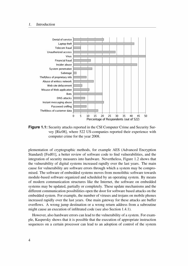
Security becomes more and more important for computers and embedded systems.With the ongoing integration of personal computers and embedded systems into net-works and finally into the Internet, security attacks on these systems arose. These net-worked, distributed devices may now compute sensitive data from the whole worldand the attacker does not need to be physically present. Also, the increased complex-ity of these devices increases the probability of errors which can be used to breakinto a system. Figure 1.1 shows a classification of different types of attacks related tocomputer systems. This information is obtained form the CSI Computer Crime andSecurity Survey [Ric08], where 522 US-companies reported their experience withcomputer crime. Further, the integration of networking interfaces into embeddeddevices, for which it would not be obviously necessary lead to strange attacks, forexample that someone can break into the coffee machine over the Internet and alterthe composition of the coffee [Wri08].
Within the last decade, the focus of the embedded software community paid moreattention onto security of software-based applications. Today, most of the softwareupdates fix security bugs and provide only little additional functionality. At the sametime, the number of embedded electronic devices including at least one processor isincreasing.
The awareness of security in digital systems lead to investigation of secure com-munication standards, for example SSL (Secure Socket Layer) [FKK96], the im-
3
1. Introduction
Denial of service
Laptop theft
Telecom fraud
Unauthorized access
Virus
Financial fraud
Insider abuse
System penetration
Sabotage
Theft/loss of proprietary info
Abuse of wirless network
Web site defacement
Misuse of Web application
Bots
DNS attacks
Instant messaging abuse
Password sniffing
Theft/loss of customer data
0 5 10 15 20 25 30 35 40 45 50Percentage of Respondents (out of 522)
Figure 1.1: Security attacks reported in the CSI Computer Crime and Security Sur-vey [Ric08], where 522 US-companies reported their experience withcomputer crime for the year 2008.
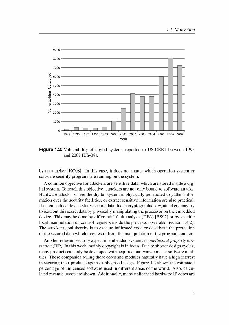
plementation of cryptographic methods, for example AES (Advanced EncryptionStandard) [Fed01], a better review of software code to find vulnerabilities, and theintegration of security measures into hardware. Nevertheless, Figure 1.2 shows thatthe vulnerability of digital systems increased rapidly over the last years. The maincause for vulnerability are software errors through which a system may be compro-mised. The software of embedded systems moves from monolithic software towardsmodule-based software organized and scheduled by an operating system. By meansof modern communication structures like the Internet, the software on embeddedsystems may be updated, partially or completely. These update mechanisms and thedifferent communication possibilities open the door for software based attacks on theembedded system. For example, the number of viruses and trojans on mobile phonesincreased rapidly over the last years. One main gateway for these attacks are bufferoverflows. A wrong jump destination or a wrong return address from a subroutinemight cause an execution of infiltrated code (see also Section 1.4.1).
However, also hardware errors can lead to the vulnerability of a system. For exam-ple, Kaspersky shows that it is possible that the execution of appropriate instructionsequences on a certain processor can lead to an adoption of control of the system
4
1.1 Motivation
1995 1996 1997 1998 1999 2000 2001 2002 2003 2004 2005 2006 20070
1000
2000
3000
4000
5000
6000
7000
8000
9000
Year
Vul
nera
bilit
ies
Cat
alog
ed
Figure 1.2: Vulnerability of digital systems reported to US-CERT between 1995and 2007 [US-08].
by an attacker [KC08]. In this case, it does not matter which operation system orsoftware security programs are running on the system.
A common objective for attackers are sensitive data, which are stored inside a dig-ital system. To reach this objective, attackers are not only bound to software attacks.Hardware attacks, where the digital system is physically penetrated to gather infor-mation over the security facilities, or extract sensitive information are also practical.If an embedded device stores secure data, like a cryptographic key, attackers may tryto read out this secret data by physically manipulating the processor on the embeddeddevice. This may be done by differential fault analysis (DFA) [BS97] or by specificlocal manipulation on control registers inside the processor (see also Section 1.4.2).The attackers goal thereby is to execute infiltrated code or deactivate the protectionof the secured data which may result from the manipulation of the program counter.
Another relevant security aspect in embedded systems is intellectual property pro-tection (IPP). In this work, mainly copyright is in focus. Due to shorter design cycles,many products can only be developed with acquired hardware cores or software mod-ules. Those companies selling these cores and modules naturally have a high interestin securing their products against unlicensed usage. Figure 1.3 shows the estimatedpercentage of unlicensed software used in different areas of the world. Also, calcu-lated revenue losses are shown. Additionally, many unlicensed hardware IP cores are
5

1. Introduction
Asia- P
acific
Centra
l & E
aste
rn E
urope
Latin
Am
erica
Mid
dle E
ast & A
frica
North
Am
erica
Wes
tern
Eur
ope
0
10
20
30
40
50
60
70
80un
licen
sed
softw
are
usag
e in
%
Asia- P
acific
Central &
Easte
rn E
urope
Latin
Am
erica
Mid
dle
East &
Afri
ca
North
Am
erica
Wes
tern
Euro
pe
0
2000
4000
6000
8000
10000
12000
14000
16000
Loss
es (
$M)
Figure 1.3: On the left side, the percentage of the usage of unlicensed software isshown in different areas of the world. On the right side the correspond-ing losses in million US-Dollars are depicted [All07].
used in products. At the RSA conference in 1998, it was estimated, that the adversityof the usage of unlicensed IP cores approaches 1 Billion US$ per day [All00].
Why Reliability?
In an integrated circuit, permanent errors and transient faults may occur. The dif-ference between defects, faults, and errors is described in Section 1.2.2. Permanenterrors are known since the invention of integrated circuits. Major causes of perma-nent errors are production defects and design errors. On the other hand, a transientfault corrupts the correct value of a signal for a short period of time. After the ef-fect’s duration, the correct value is usually recovered and the circuit is not physicallydamaged. Transient faults can be caused by on-chip perturbations, like power supplynoise or external noise [NX06]. The main cause for external noise inside the earth’satmosphere are high energy neutrons from cosmic ray interactions and alpha parti-cles from nuclear reactions. In space, the main source for radiation are high energycosmic rays and high energy protons from trapped radiation belts [Joh00]. Transientfaults caused by radiation are also called soft errors in the literature (see also Section1.3.4).
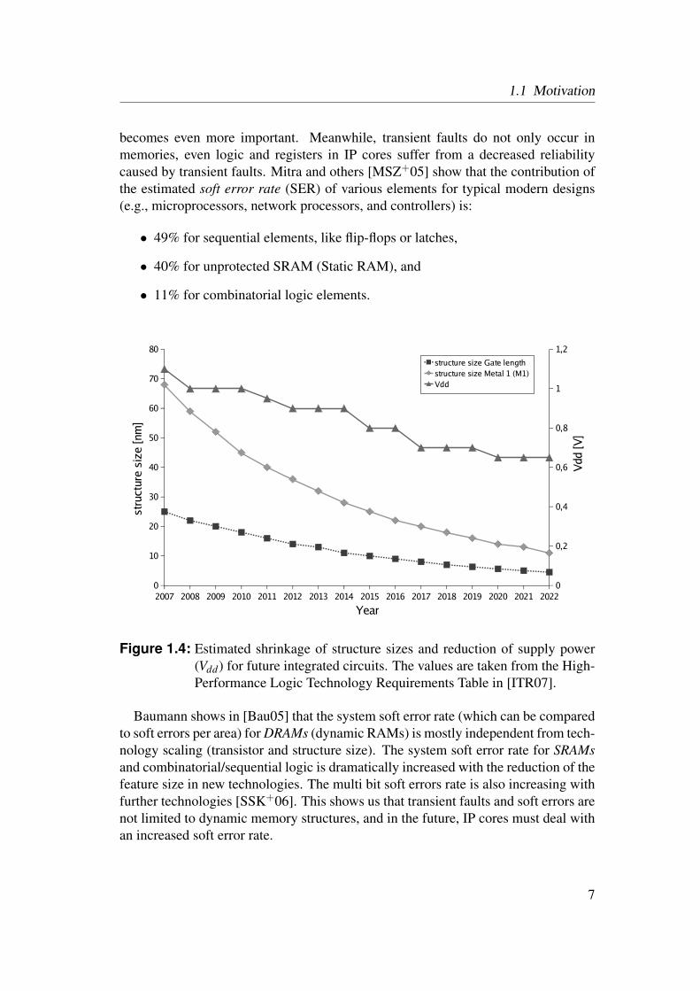
Dynamic memory structures are particularly sensitive to transient faults. Since the1970s, developers have dealt with soft errors in large dynamic memory structures[GWA79]. With the ongoing shrinkage of transistor sizes and on-chip structures andthe reduced power supply voltage (see Figure 1.4), the problem of transient faults
6
1.1 Motivation
becomes even more important. Meanwhile, transient faults do not only occur inmemories, even logic and registers in IP cores suffer from a decreased reliabilitycaused by transient faults. Mitra and others [MSZ+05] show that the contribution ofthe estimated soft error rate (SER) of various elements for typical modern designs(e.g., microprocessors, network processors, and controllers) is:
• 49% for sequential elements, like flip-flops or latches,
• 40% for unprotected SRAM (Static RAM), and
• 11% for combinatorial logic elements.
2007 2008 2009 2010 2011 2012 2013 2014 2015 2016 2017 2018 2019 2020 2021 20220
10
20
30
40
50
60
70
80
0
0,2
0,4
0,6
0,8
1
1,2
structure size Gate lengthstructure size Metal 1 (M1)Vdd
Year
stru
ctur
e si
ze [n
m]
Vdd
[V]
Figure 1.4: Estimated shrinkage of structure sizes and reduction of supply power(Vdd) for future integrated circuits. The values are taken from the High-Performance Logic Technology Requirements Table in [ITR07].
Baumann shows in [Bau05] that the system soft error rate (which can be comparedto soft errors per area) for DRAMs (dynamic RAMs) is mostly independent from tech-nology scaling (transistor and structure size). The system soft error rate for SRAMsand combinatorial/sequential logic is dramatically increased with the reduction of thefeature size in new technologies. The multi bit soft errors rate is also increasing withfurther technologies [SSK+06]. This shows us that transient faults and soft errors arenot limited to dynamic memory structures, and in the future, IP cores must deal withan increased soft error rate.
7

1. Introduction
Another challenge to build reliable embedded systems in the future is the increas-ing process variability. The random dopant fluctuation of transistors will increase infuture technologies, because of the discreteness of dopant atoms in the gate channel[Bor05]. The left side of Figure 1.5 shows the mean number of dopant atoms in atransistor channel over varying technology sizes. In the 32 to 16 nm technology gen-eration, we will have only tens of dopant atoms. A small variation of dopant atomsmay cause a huge variation of the transistor properties. The second source for tran-sistor variations is sub-wavelength lithography, which results in line-edge roughnessand several other effects, which may cause transistor variations [Bor05]. The righthand side of Figure 1.5 shows possible transistor variation increasing in the future.
Figure 1.5: On the left side, the mean number of dopant atoms in a transistor chan-nel is shown over different technologies. The right side shows the actualand the possible future variation of the threshold voltage Vt of transis-tors. Both figures are taken from [Bor05].
Also, the power dissipation density will increase into dimensions of over 100 Wcm2 .
Future technologies expand the distribution of physical parameters (e.g., tox, Le f f ,We f f , doping, Vt) disproportionately. The timing is only predictable in a small rangebecause of the variation of the wire delays by increased synchronization errors. Theseerrors are caused by different voltage or clock islands, and by massive capacitive/in-ductive crosstalk. The consequences are decreased reliability and a lifetime of com-plex, very large scale integration systems and dramatically decreasing yield of todaysstrategies. A design flow assuming the worst-case is not applicable in the future, be-cause this results in a design with a large power consumption which has a high impacton reliability.
This shows us that transistors will get more and more unreliable in the future. Thegreat challenge is to design reliable systems from unreliable components [Bor05].In conclusion, reliability in embedded systems is getting increasingly important. Inthe past, the need for additional functions to improve the reliability of the systemby monitoring and correcting errors was only given for safety-critical systems whichmust have a high fault tolerance like banking mainframes, control systems of nuclear
8

1.1 Motivation
plants or chip cards. In the future, the need for reliability-preserving and -increasingtechniques will also become substantial for consumer products, like personal com-puters or, in our case, embedded systems.
Why IP Cores?
With every new chip generation, the logic density and thus the chip complexity interms of transistors per chip rapidly increases (see Figure 1.6). This growth is higherthan the design productivity increase of the last years. Additionally, the market re-quires shorter product cycles, which intensify this problem. This creates the designproductivity gap between what we are able to build and what we can design. To closethe gap, many innovations in design technologies are applied to increase the produc-tivity. One of these innovations is the reuse of IP cores, which boosts the productivityof a design team by 200% according to [ITR07]. Only by reusing IP cores are weable to keep up future design productivity with the technologies improvements inchip manufacturing (see Figure 1.6).
2005 2006 2007 2008 2009 2012 2015 20180
500
1000
1500
2000
2500
0
2
4
6
8
10
12
14transistor density [Mtransistor/cm^2]productivity [Mtranistors/(100*designer*year)]design cycle [month]
Year
Mill
ion
Tran
sist
ors
mon
th
Figure 1.6: The increasing transistor density in MTranistorscm2 and the productivity in
MTransitors per design year with a team of 100 designers are shown.Also, the design cycle in months is depicted [ITR05].
Previously designed cores, like CPUs, buses, or cryptographic cores can be reusedby new projects or sold as IP cores to other users. The advantage besides the increasedproductivity is that designers or whole companies have the possibility of specializing
9

1. Introduction
on specific cores which may introduce an additional unique feature. Many companiesbase their business model on the sale of IP cores (e.g., ARM). Figure 1.7 shows thetrend of rising core reuse in digital designs.
2007 2008 2009 2010 2011 2012 2013 2014 2015 2016 2017 2018 2019 2020 2021 20220
10
20
30
40
50
60
70
Year
desi
gn r
euse
[%]
Figure 1.7: The percentage of reused IP cores compared to all designed logic willbe raised in the future [ITR07].
IP cores can be delivered at different design levels. Possible distribution levels areRTL (e.g., VHDL or Verilog code), logic (e.g., EDIF netlists), or device level (e.g.,layouts for ASICs or bitfiles for FPGAs). To improve the design and trade of IP coresas well as the interface between IP cores, the Virtual Socket Interface (VSI) Alliancewas founded in 1996 [See99]. The VSI Alliance accounts for significant barriersfor the trade with IP cores. One of these barriers is the lack of protection againstunlicensed usage [All00].
Future IP cores should not only be resistant against unlicensed usage. They shouldalso integrate state of the art reliability and security features at IP core level, such asautonomic error detection and correction methods.
Why FPGAs?
FPGAs (Field Programmable Gate Arrays) have their roots in the area of PLDs (Pro-grammable Logic Devices), such as PLAs (Programmable Logic Arrays) or PALs(Programmable Array Logics). Today, FPGAs have a significant market segment inthe microelectronics and, particularly in the embedded system area. The advantagesof FPGAs over ASICs are their flexibility, the reduced development costs, and theshort implementation time. Also, developers have a limited implementation risk, a),because of the easy possibility to update an erroneous design and b), because of the
10

1.1 Motivation
awareness, that the silicon devices are proofed and the underlying technology oper-ates correctly under the specified terms.
The main advantage of FPGAs is their reconfigurability. The demand for flexi-bility through reconfigurability will rise according to ITRS [ITR07] from 28% of allfunctionalities in 2007 until to an estimated 68% in the year 2022. Note that ITRSalso takes into account software running on a microprocessor which can be updated.Furthermore, many FPGA devices support dynamic partial reconfiguration, whichmeans that during runtime, the design or a part of it can be reconfigured. With thisadvantage, we can envisage new designs with new and improved possibilities andproperties, like an adaptive design, which can adapt itself to a new operation envi-ronment. Unfortunately, dynamic reconfiguration is currently used rarely due to thelack of improved design tools which increases the development costs for dynamic re-configuration. But now, improved design tools for partial reconfiguration are startingto become available, like the ReCoBus-Builder [KBT08, KHT08] or Xilinx Plana-head [DSG05]. Nevertheless, dynamic reconfiguration for industrial designs is in itsinfancy, and it will take several years to use all the great features of FPGAs.
In the last years, the main application area of FPGAs were in small volume em-bedded systems and rapid prototyping platforms, where ASIC designs can be im-plemented and verified before the expensive masks are produced. Nevertheless, theFPGA usage in higher volume market rises, mainly due to lower FPGA price, higherlogic density and lower power consumption. Furthermore, due to shorter time-to-market cycles (see Figure 1.6) and rising ASIC costs, FPGAs are breaking more andmore into traditional ASIC domains. On the other hand, FPGAs are becoming com-petitors in the (reconfigurable) DSP domain with multi-core and coarse-grain recon-figurable architectures, as well as from graphic processing units (GPU) where DSPalgorithms are adapted to run on these architectures. Nevertheless, these architec-tures suffer from the lack of flexibility and today, only FPGA technology is flexibleenough to implement a heterogeneous reconfigurable system-on-a-chip.
Why ASICs?
Besides the advantages and the success of FPGAs, there still exists a huge market fortraditional ASICs (Application Specific Integrated Circuit). ASICs are designed forhigh volume productions, where small cost-per-unit is important, as well as in lowpower and high performance applications and designs with a high logic density.
The implementation of a core on an ASIC instead of an FPGA (both 90 nm tech-nology) may require 40 times less area, may speed up the critical path by a factorbetween 3 and 4, and may reduce the power by a factor of about 12 [KR06]. Here,we see that the big advantage of ASICs over FPGAs is the higher logic density, whichresults in significantly lower production cost per unit. The disadvantages of ASICsare the higher development and the higher initial production costs (e.g., masks, pack-age design, test development [Kot06]). Therefore, the decision for using ASICs or
11
1. Introduction
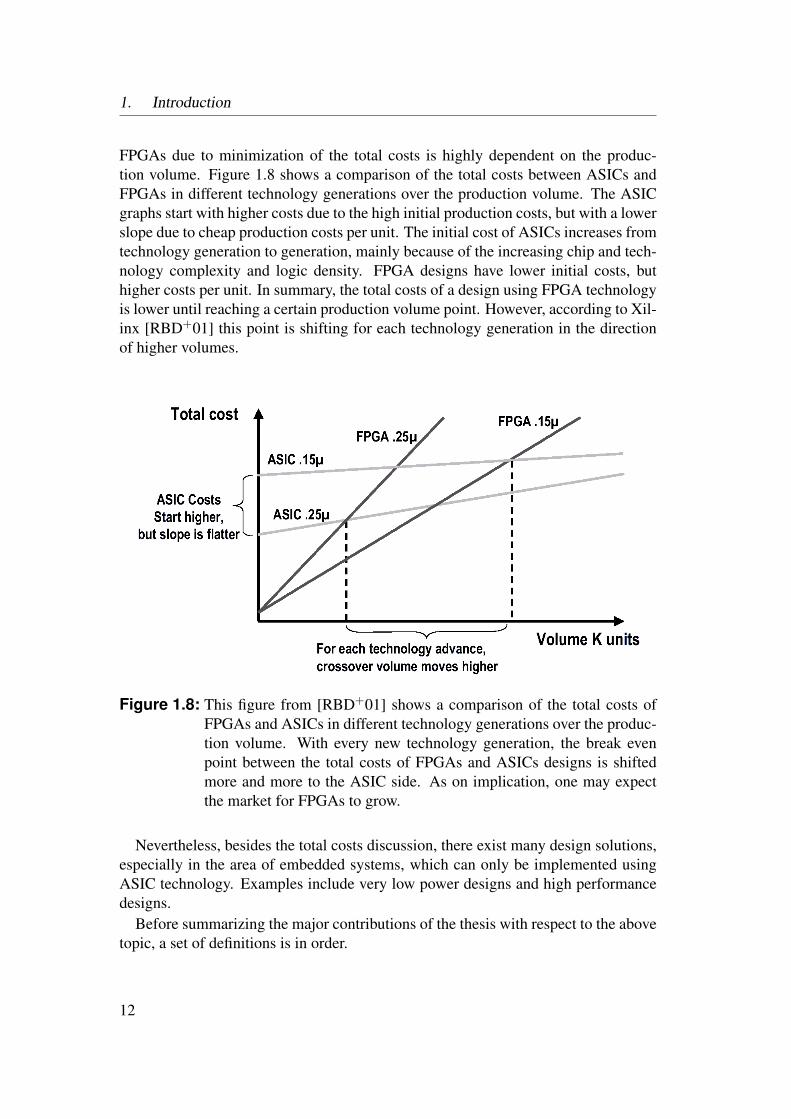
FPGAs due to minimization of the total costs is highly dependent on the produc-tion volume. Figure 1.8 shows a comparison of the total costs between ASICs andFPGAs in different technology generations over the production volume. The ASICgraphs start with higher costs due to the high initial production costs, but with a lowerslope due to cheap production costs per unit. The initial cost of ASICs increases fromtechnology generation to generation, mainly because of the increasing chip and tech-nology complexity and logic density. FPGA designs have lower initial costs, buthigher costs per unit. In summary, the total costs of a design using FPGA technologyis lower until reaching a certain production volume point. However, according to Xil-inx [RBD+01] this point is shifting for each technology generation in the directionof higher volumes.
Figure 1.8: This figure from [RBD+01] shows a comparison of the total costs ofFPGAs and ASICs in different technology generations over the produc-tion volume. With every new technology generation, the break evenpoint between the total costs of FPGAs and ASICs designs is shiftedmore and more to the ASIC side. As on implication, one may expectthe market for FPGAs to grow.
Nevertheless, besides the total costs discussion, there exist many design solutions,especially in the area of embedded systems, which can only be implemented usingASIC technology. Examples include very low power designs and high performancedesigns.
Before summarizing the major contributions of the thesis with respect to the abovetopic, a set of definitions is in order.
12

1.2 Definitions
1.2 Definitions
In this section, we introduce necessary definitions of terms with respect to securityand reliability of embedded systems that will be throughout this thesis. First, defi-nitions in the field of dependability and the difference between defects, faults, anderrors are outlined. After the categorization of faults and errors, definitions stem-ming from the area of security attacks are presented. Finally, different types of over-head, which are indispensable for additional security and reliability functions, aredescribed.
1.2.1 Dependability and its Attributes
The dependability of a system is defined by the IFIP 10.4 Working Group on De-pendable Computing and Fault Tolerance as: “... the trustworthiness of a comput-ing system which allows reliance to be justifiably placed on the service it delivers...” [IFI90]. According to Laprie and others [ALR01], the concept of dependabil-ity consists of three parts: the threats to, the attributes of, and the means by whichdependability is attained (see Figure 1.9).
Dependability Means
Attributes
Threats
Safety
Reliability
Availability
Maintainability
Integrity
Confidentiality
Fault Prevention
Fault Forecasting
Fault Removal
Fault Tolerance
Failures
Errors
Faults
Figure 1.9: The relationship of dependability between attributes, threats and means[ALR01].
The attributes of dependability are a way to assess the trustworthiness of a sys-tem. The attributes are: availability, reliability, safety, confidentiality, integrity, andmaintainability.
13

1. Introduction
Availability
The availability is considered as the readiness for correct service [ALR01]. Thismeans that the availability is a degree of the possibility to start a new function ortask of the system. Usually, the availability is given in the percentage of time thata system is able of serving its intended function and can be calculated using thefollowing formula:
Availability =Total Elapsed Time−Down Time
Total Elapsed Time(1.1)
Availability is also often measured in “nines”. Two nines means an availability of99%, three nines means 99.9% and so on. Table 1.1 shows the maximal downtimewithin a year for different availability values.
Availability Percentage 8-hour day 24-hour dayTwo nines 99% 29.22 hours 87.66 hours
Three nines 99.9% 2.922 hours 8.766 hoursFour nines 99.99% 17.53 mins 52.60 minsFive nines 99.999% 1.753 mins 5.260 minsSix nines 99.9999% 10.52 secs 31.56 secs
Table 1.1: The maximal annual downtime of a system for different values of avail-ability, running either 8 hours or 24 hours per day [Rag06].
Reliability
Reliability is defined as the ability of a system or component to perform its requiredfunctions under well-defined conditions for a specified time period [Ger91]. Laprieand others transcribe the reliability with the continuity of correct service [ALR01].Important parameters of reliability are the failure rate and its inversion, the MTTF(mean time to failure). Other parameters, like the MTBF (mean time between fail-ures) include the time which is necessary to repair the system. The MTBF is the sumof MTTF and the MTTR (mean time to repair).
Safety
Safety is the attribute of a safe system. This means that the system cannot lead tocatastrophic consequences for the users or the environment. Safety is relative, theelimination of all possible risks is usually impossible. Furthermore, the safety ofa system cannot be measured directly. It is rather a subjective confidence of thesystem. Whereas availability and reliability avoid all failures, safety avoids only thecatastrophic failures, which are only a small subset.
14

1.2 Definitions
Confidentiality
The confidentiality of a system describes the absence of unauthorized disclosure ofinformation. The International Organization of Standardization (ISO) defines theconfidentiality as “ensuring that information is accessible only to those authorizedto have access” [ISO05]. In many embedded systems (e.g., cryptographic systems),it is very important to secure the information (e.g., the secure key) stored inside thesystem against unauthorized access. But also the prevention of unlicensed usage ofsoftware programs or hardware cores are topics of confidentiality. Confidentiality is,like safety, subjective and cannot be measured directly.
Integrity
Integrity is the absence of improper system state alternation. This alternation canbe an unauthorized access to alter system information inside the system, which arenecessary for the correctness of the system. Furthermore, the system state alternationcan also be a damage or modification of the system. System integrity assures that nopart of the system (software or hardware) can be altered without the necessary privi-leges. Also, the IP core verification to ensure the correct creator and the absence ofunauthorized supplementary changes can elevate the integrity of a system. Integrityis the precondition for availability, reliability and safety [ALR01].
Maintainability
Maintainability is the ability to undergo repairs and modifications. This can be doneto repair errors, meet new requirements, make further maintenance easier, or to copewith a changed requirement or environment. A system with a high maintainabilitymay have a good documentation, a modular structure, is parameterizable, uses asser-tions and implements built-in self tests.
Security
Security is defined as a combination of the attributes (1) confidentiality (the preven-tion of the unauthorized disclosure of information), (2) integrity (the prevention ofthe unauthorized amendment or deletion of information), and (3) availability (theprevention of the unauthorized withholding of information) [ITS91]. An alternativedefinition for security could be the absence of unauthorized access to the system state[ALR01]. The prevention or detection of the usage of unlicensed software or IP corescan also be seen as a security aspect (confidentiality) as well as the prevention of theunauthorized alteration of software or IP cores (integrity). Like safety, security shallprevent only a class of failures which are caused by unauthorized access or unautho-rized handling of information.
15
1. Introduction
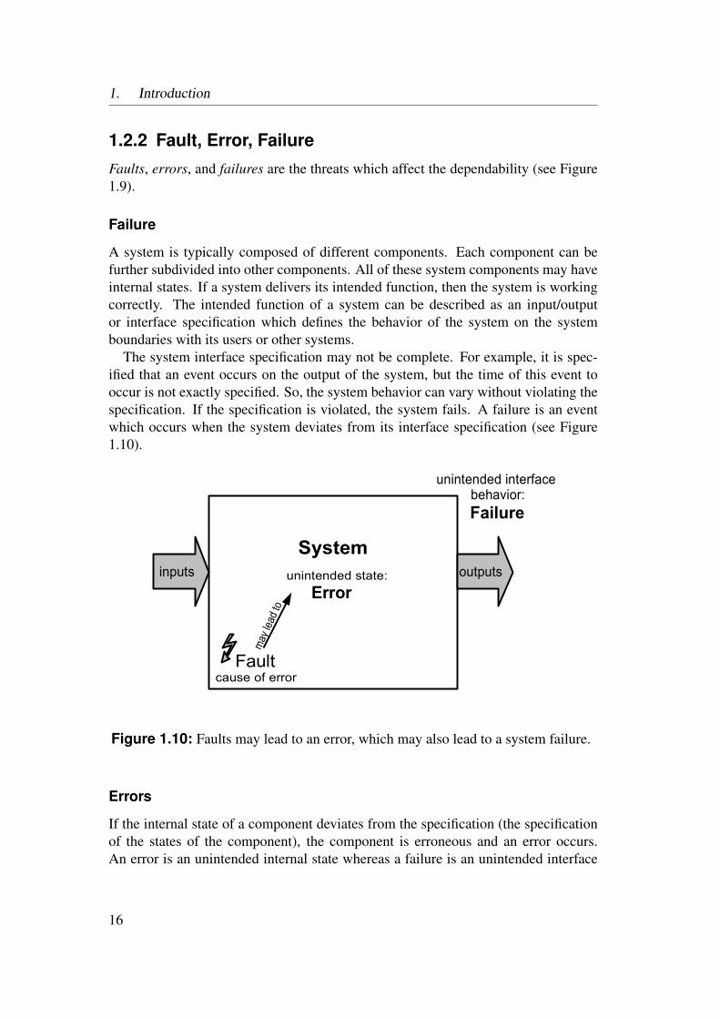
1.2.2 Fault, Error, FailureFaults, errors, and failures are the threats which affect the dependability (see Figure1.9).
Failure
A system is typically composed of different components. Each component can befurther subdivided into other components. All of these system components may haveinternal states. If a system delivers its intended function, then the system is workingcorrectly. The intended function of a system can be described as an input/outputor interface specification which defines the behavior of the system on the systemboundaries with its users or other systems.
The system interface specification may not be complete. For example, it is spec-ified that an event occurs on the output of the system, but the time of this event tooccur is not exactly specified. So, the system behavior can vary without violating thespecification. If the specification is violated, the system fails. A failure is an eventwhich occurs when the system deviates from its interface specification (see Figure1.10).
System
Faultcause of error
unintended state:Error
may l
ead t
o
inputs outputs
unintended interfacebehavior:Failure
Figure 1.10: Faults may lead to an error, which may also lead to a system failure.
Errors
If the internal state of a component deviates from the specification (the specificationof the states of the component), the component is erroneous and an error occurs.An error is an unintended internal state whereas a failure is an unintended interface
16
1.2 Definitions
behavior of the system. An error may lead to a failure. But it is also possible thatan error occurs and does not lead to a system failure, because of the component iscurrently not used or the error is detected and corrected fast enough. Errors can betransient or permanent. Transient errors caused by transient faults usually occur insystems without feedback. In systems with feedback, an error might be permanentby affecting all following states. In this case, the error only disappears by a reset orby shut down of the system.
Faults
A fault is defined as a defect that has the potential to cause an error [Jal94]. All errorsare caused by faults, but a fault may not lead to an error. In the latter case, the faultis masked out and has no impact on the system.
For example, consider the control path of a processor core. A fault like a singleevent transient fault, caused by an alpha particle impact, occurs on one signal of theprogram counter between two pipeline stages. If the time of occurrence is near therising active clock edge, an error may occur. Otherwise, if the time of occurrenceis far away form the rising edge of the clock, the fault does not lead to an error.The erroneous program counter value can now lead to a system failure, if the wrongsubroutine is executed and the interface behavior differs from the specification. Oth-erwise, if an error detection technique, like a control flow checker, as introduced laterin Chapter 4, is used, the error can be detected after the fault appearance, and theerror may be corrected by a re-execution of the corresponding instruction. But, thisadditional re-execution needs several clock cycles to restore the error free state. Forreal-time systems with very critical timing requirements, the possible output eventsmight be too late and the system thus might still fail.
1.2.3 Fault and Error Categorization
Faults can be categorized into different classes. The main classes are: persistence,nature, and origin (see Table 1.2) [ALRL04, Kop97].
Faults Errorspersistence nature origin location effectpermanent chance development e.g. data path value
sporadic transient intentional runtime control path timingperiodic transient memory
Table 1.2: An overview of different faults and error classes.
The persistence of a fault can be permanent or transient. The class of transientfaults can be further subdivided into sporadic and periodic faults. A permanent fault
17
1. Introduction
is, for example, a broken wire. Alpha particle radiation on a chip can cause sporadictransient faults, and jitter in a clock signal is a periodic transient fault. It is importantto know that transient faults can also lead to permanent errors. The nature of thefault can be chance or intentional. A chance fault occurs randomly with a specificprobability, like faults from radiation. An intentional fault can be a security attack to asystem or a faulty operation from the user. Intentional faults can be further subdividedinto malicious intentional faults and non-malicious intentional faults (more about thisin Section 1.2.5). The origin of a fault can be in the development phase of the systemor at runtime. Physical phenomena like lightning strokes belong to runtime faults,whereas, design faults are caused in the development phase.
Errors can be categorized into different error classes (see Table 1.2). Here, we dis-tinguish between the location and the effect class. Errors can be classified accordingto the location or components of their occurrence, for example, data path or controlpath errors. Value errors and timing errors belong to the effect class. For example,a value error occurs when an incorrect value of a register is caused by a single eventupset, whereas a timing error occurs if the delay of a signal is too large, caused, forexample, by a too high temperature.
There exist many other definitions of fault and errors classes in literature. Thepresented classes above present a minimal intersection between these different defi-nitions.
1.2.4 Means to Attain Dependability
Means are ways to increase the dependability of a system. There exist four means,namely fault prevention, fault tolerance, fault removal, and fault forecasting.
Fault Prevention
Fault prevention deals with the question “How the occurrence or introduction of faultscan be prevented?”. Design fault might be prevented with quality control techniquesduring the development and manufacturing of the software and hardware of a system.Fault prevention is further closely related to maintainability. Transient faults, likesingle event effects, might be reduced by shielding, radiation hardening, or largerstructure sizes. Attacks might be prevented by security measures, like firewalls oruser authentication. To prevent the usage of unlicensed programs or IP cores, the code(source, binary, or netlist code) could be delivered encrypted and only the authorizedcustomer has the right cryptographic key to decrypt the code. To prevent the impartof the key, techniques like dongles or an authentication with MAC-Address can beused.
18
1.2 Definitions
Fault Tolerance
A fault-tolerant system does not fail, even if an erroneous state is reached. Faulttolerance enables a system to continue operation in the case of one or more errors.This is usually implemented by error detection and system recovery to an error-freestate. In a fault tolerant system, errors may occur, but they must be handled correctlyto prevent a system failure.
The first step towards a fault tolerant system is error detection. Error detectioncan be subdivided into two classes: concurrent error detection and preemptive errordetection [ALR01]. Concurrent error detection takes place at runtime during theservice delivery, whereas preemptive error detection runs in phases where the servicedelivery is suspended. Examples for concurrent error detection are error codes (e.g.parity or CRC), control flow checking, or razor flip-flops [ABMF04].
Also, redundancy belongs to this class of error detection. One may distinguishthree types of redundancy: hardware, time and information redundancy. To detecterrors with hardware redundancy, we need at least two units where both results arefinally compared. If they divert, an error occurred. On time redundancy, the systemexecutes the same inputs twice, and both results are compared after the second ex-ecution. Information redundancy uses additional information to detect errors (e.g.,parity bits). More information about redundancy methods can be found in Section2.3.
BISTs (Built In Self Tests) or start-up checks belong to the preemptive error detec-tion class.
The next step is the recovery from the erroneous state. Recovery consists of twosteps, namely error handling and fault handling. Error handling is usually accom-plished by rollback or rollforward. Rollback is done by using error-free states whichare stored on certain checkpoints to restore the state of the system to an older error-free state. Rollback is attended by delaying the operation. This might be a problemin case of real-time applications. Rollforward uses a new error-free state to recoverthe system.
If the cause of the error is a permanent or periodic temporal fault, we need faulthandling to prevent the system from running into the same error state repeatedly. Thisis usually done by fault diagnosis, fault isolation, system reconfiguration and systemreinitialization. For example, in case at permanent errors in memory structures, thefaulty memory column is identified and this column is switched to a reserved sparecolumn. After the switch over, the column content must be reinitialized.
It is important to notice that fault tolerance is a recursive concept. The techniquesand methods which provide fault tolerance should obviously themselves be resistantagainst faults. This can, for example, be done by means of replication.
19
1. Introduction
Fault Removal
During the development phase and during the operational runtime, fault removalmight be performed. At the development phase, fault removal consists of the fol-lowing steps: verification, diagnostics, and correction [ALR01]. This is usually doneby debugging and/or simulation of software and hardware. For the verification offault tolerant systems, fault injection (see Section 4.2) can be used.
Fault removal during the operational runtime is usually done by maintenance.Here, faults can be removed by software updates or by the replacement of faultysystem parts.
Fault Forecasting
Fault forecasting predicts feasible faults to prevent or avoid the fault or decreasethe effect of the fault. This can be done by performing an evaluation of the systembehavior with respect to fault occurrence and effects. Modeling and simulation of thesystem and faults are a common way to achieve this evaluation.
1.2.5 Security Flaws and Attacks
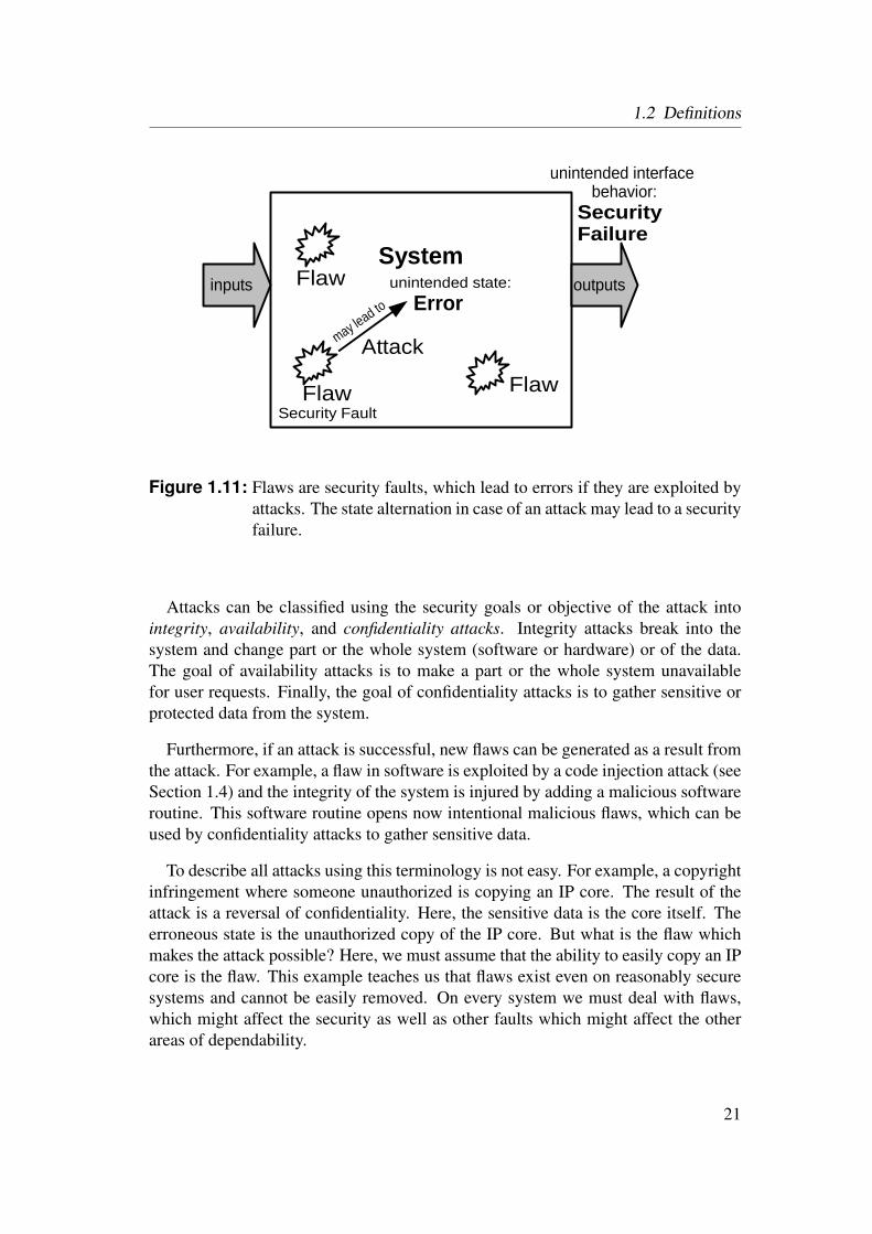
Faults affecting the security of a system are also called flaws [LBMC94]. In thiswork, the term flaw is used as a synonym of a fault, which leads to the degenerationof the security of a system. A flaw is therefore a weakness of the system whichcould be exploited to alter the system state (error). A threat is a potential eventwhich might lead to this alternation and therefore to a security failure. The process ofexploiting the flaw by a threat is called an attack (see Figure 1.11). A security failureoccurs when a security goal is violated. The main security goals are the dependabilityattributes integrity, availability, and confidentiality. The difference between a flawand a threat is that a flaw is a system characteristic, whereas a threat is an externalevent.
A flaw can be intentional or inadvertent. Intentional flaws can further be mali-cious or non-malicious. An intentional malicious flaw is, for example, a trojan horse[And72]. An intentional non-malicious flaw could be a communication path in acomputer system which is not intended as such by the system designer [LBMC94].An inadvertent flaw could be, for example, a bug in a software program, which en-ables unauthorized persons with specific attacks to read protected data.
Like other faults, flaws can also be further categorized using the origin of the flawand the persistence. The origin can be during the development (e.g., the developerimplement a back door to the system), or during operation or maintenance. Usually,the flaws exist for a longer period of time (e.g., from the flaw arise until the flaw isdisappeared by a security update). But also special flaws exists, which only appear oncertain situations (e.g., the year 2000 problem; switching from year 1999 to 2000).
20
1.2 Definitions
System
FlawSecurity Fault
unintended state:
Error
may lead to
inputs outputs
unintended interfacebehavior:
SecurityFailure
Attack
Flaw
Flaw
Figure 1.11: Flaws are security faults, which lead to errors if they are exploited byattacks. The state alternation in case of an attack may lead to a securityfailure.
Attacks can be classified using the security goals or objective of the attack intointegrity, availability, and confidentiality attacks. Integrity attacks break into thesystem and change part or the whole system (software or hardware) or of the data.The goal of availability attacks is to make a part or the whole system unavailablefor user requests. Finally, the goal of confidentiality attacks is to gather sensitive orprotected data from the system.
Furthermore, if an attack is successful, new flaws can be generated as a result fromthe attack. For example, a flaw in software is exploited by a code injection attack (seeSection 1.4) and the integrity of the system is injured by adding a malicious softwareroutine. This software routine opens now intentional malicious flaws, which can beused by confidentiality attacks to gather sensitive data.
To describe all attacks using this terminology is not easy. For example, a copyrightinfringement where someone unauthorized is copying an IP core. The result of theattack is a reversal of confidentiality. Here, the sensitive data is the core itself. Theerroneous state is the unauthorized copy of the IP core. But what is the flaw whichmakes the attack possible? Here, we must assume that the ability to easily copy an IPcore is the flaw. This example teaches us that flaws exist even on reasonably securesystems and cannot be easily removed. On every system we must deal with flaws,which might affect the security as well as other faults which might affect the otherareas of dependability.
21
1. Introduction
1.2.6 OverheadMethods for increasing security and reliability in embedded systems often have thedrawback of additional overhead. To evaluate the additional costs of these methods,we can use the following criteria:
• Area overhead (hardware cost overhead),
• Memory overhead, and
• Execution time overhead (CPU time).
Analysis and quantification of the additional costs significantly depends on thegiven architecture and the implementation on a specific target technology.
Area Overhead
The straightforward method for measuring the area overhead of an additional core isto measure the chip area occupied by the core. Unfortunately, this method can onlycompare cores implemented in the same technology with exactly the same process(lateral dimensions). To become independent of this process, the transistor countmay be used. However, information about the area of the signal routing is not in-cluded here. In most of the technologies and processes, signal routing requires littleadditional area because of the routing layers are above the transistors (in the thirddimension). This also depends on the specific process.
The number of transistors, however, is a reasonable complexity indicator, only ifthe compared cores use the same technology (e.g., CMOS, bipolar). To compare thehardware costs of a core mapped onto different technologies, the gate count can beused. Here, the number of logical (two input) gates is used to describe the hardwarecosts. For comparing cores between ASIC and FPGA technologies, the count ofprimitive components or operations, like n-bit adders or multipliers, can be used.
Using primitive components or operations for the description of the overhead, oneis independent of the underlying technology and process. Describing hardware costin a higher hierarchy level, like primitive components or operations, however, is moreinaccurate with respect to the real hardware costs than describing the overhead in chiparea. The resulting chip area of the used primitive components depends highly on thetechnology and process and also on the knowledge of the chip designer or the qualityof the tools.
Memory Overhead
The memory overhead for methods increasing the security and reliability can be mea-sured by counting the additional ram bits used by the corresponding method. Mem-ories embedded on the chip, so called internal memories, use hardware resources on
22
1.2 Definitions
the chip and so they contribute to the area overhead. Nevertheless, the content ofmemories can be relatively easily shifted to a cheaper external memory, for examplean off-chip system DRAM. So, we decided to handle the memory overhead sepa-rately. It must be taken into account that internal memory has higher hardware costsat the same size, but a lower latency. External memory is usually cheaper, but it in-volves additional hardware costs on the chip, as for example a DRAM controller. If aDRAM with the corresponding controller already exists on the chip, these resourcesmight be shared to reduce the hardware cost.
Execution Time Overhead
Some methods for increasing the security and reliability have additional latency. Thismeans that the result of the protected core or software appears later on the outputsthan on the unprotected one. For hardware cores, latency is usually counted in ad-ditional clock cycles. For software programs, latency can be expressed in additionalinstructions which must be executed by the processor or in additional execution timeof the processor. For example, some existing methods for control flow checking[GRRV03] generate additional instructions that are inserted into the original programrunning on the processor which is monitored. This might cause a timing impact forthe user program which impact can be measured by additional execution time of theprocessor. The execution time depends on the processor and the number of executedadditional instructions.
Also, if no additional software is executed on the processor and the processor isenhanced with additional hardware, some methods can stall [ZT09] the processorpipeline, slow down the execution of the user program, or insert additional pipelinesteps [Aus99] without executing additional instructions.
For processor architectures, the execution time overhead can be measured by count-ing the additional pipeline steps. If the processor architecture executes one instruc-tion in one pipeline step (in the best case one clock cycle), the number of additionalexecuted instructions are also given in the number of additional pipeline steps.
1.2.7 IP Cores and Design Flow
The reuse of IP cores is an important step to decrease the productivity gap, whichemerges from the rapid increase of the chip complexity and the slower growth of thedesign productivity. Today, there is a huge market and repertoire of IP cores whichcan be seen in special aggregation web sites, for example [Reu] and [Est], whichadministrate IP core catalogs.
The delivery format of IP cores is closely related to the design flow. The designflow consists of different design flow or abstraction levels which transfer the descrip-tion of the core from the level where the core is specified into the final implementa-
23

1. Introduction
tion. The design flow is dependent from the target technology. The FPGA and theASIC design flow look similar, however, there exist differences at some steps.
Figure 1.12 shows a general design flow for electronic designs with FPGA andASIC target technologies. This design flow view can be embedded into a highersystem model view for hardware/software co-design, for example the double roofmodel introduced by Teich [TH07]. The depicted design flow implements the logicsynthesis and the following steps in the double roof model. Furthermore, the differentabstraction levels are derived from the Y-diagram, introduced by Gaijski [GDWL92].
RTL levelHDLs, e.g., VHDL, Verilog
Logic level
Device level
Synthesis
Implementation
Netlists, e.g., EDIF
Bitfiles (FPGA), Layouts (ASIC), e.g., Mask files, ...
Figure 1.12: A general design flow for FPGA and ASIC designs with the synthesisand implementation steps and the different abstraction levels.
The different abstraction levels are the register-transfer level, the logic level, aswell as the device level. Designs specified at the register-transfer level (RTL) are usu-ally described in Hardware Description Languages (HDLs) like VHDL or Verilog,whereas designs at the logic level are usually represented in netlists, for example,Electronic Design Interchange Format (EDIF) netlists. At the device level, FPGAdesigns are implemented into bitfiles, while ASIC designs are usually represented bytheir chip layout description. The transformation of an HDL-model into an netlist-model is called logic synthesis, whereas the transformation of a netlist-model into atarget depended circuit is called implementation. The implementation consists of theaggregation of the different netlist cores and subsequent place and route step. Thetechnology mapping can be done in the synthesis or in the implementation step, orin both. For example, the Xilinx FPGA design flow maps the logic to device de-pendent primitive cells (LUT2, FF, etc.) in the synthesis step, whereas the mappingof these primitive cells to slices and configurable logic blocks (CLBs) is done in theimplementation step [Xilb].
24
1.3 Faults in Embedded Systems
IP cores can be delivered at all different abstraction levels in the correspondingformat: on the RTL as VHDL or Verilog code, on logic level as EDIF netlist, oron the device level as mask files for the ASIC flow or as FPGA depended (partial)bitfiles.
IP cores can be further categorized into soft and hard cores. Hard cores are readyto use and are offered into a target depended layout or bitfile. All IP cores which aredelivered into an HDL or netlist format belongs to the soft cores. These cores needfurther transformations of the design flow to be usable. The advantages of soft coresare their flexibility for different target technologies and their can be parameterizable.However, the timing and the area overhead are less predictable compared to hardcores due the impact of the needed design tools. Analog or mixed signal IP cores areusually delivered as hard cores.
1.3 Faults in Embedded Systems
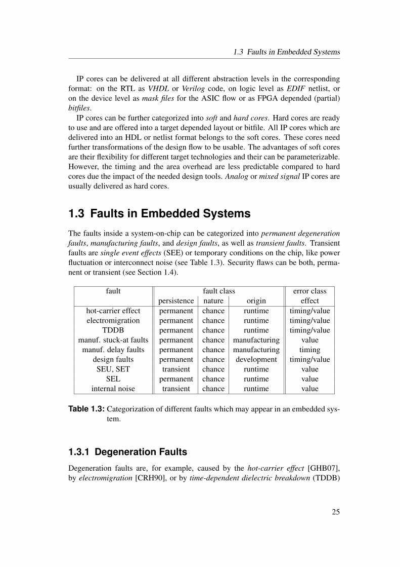
The faults inside a system-on-chip can be categorized into permanent degenerationfaults, manufacturing faults, and design faults, as well as transient faults. Transientfaults are single event effects (SEE) or temporary conditions on the chip, like powerfluctuation or interconnect noise (see Table 1.3). Security flaws can be both, perma-nent or transient (see Section 1.4).
fault fault class error classpersistence nature origin effect
hot-carrier effect permanent chance runtime timing/valueelectromigration permanent chance runtime timing/value
TDDB permanent chance runtime timing/valuemanuf. stuck-at faults permanent chance manufacturing valuemanuf. delay faults permanent chance manufacturing timing
design faults permanent chance development timing/valueSEU, SET transient chance runtime value
SEL permanent chance runtime valueinternal noise transient chance runtime value
Table 1.3: Categorization of different faults which may appear in an embedded sys-tem.
1.3.1 Degeneration Faults
Degeneration faults are, for example, caused by the hot-carrier effect [GHB07],by electromigration [CRH90], or by time-dependent dielectric breakdown (TDDB)
25

1. Introduction
[San]. All these faults are permanent chance runtime faults which at first lead to tim-ing errors and later, particularly electromigration, to value errors like open or shortcircuits.
Electromigration is caused by ion movement in the direction of the current flow[NX06, CRH90]. This leads to voids, which are able to open signal lines as well asmounds which have the ability to short the signal with an adjacent signal. Especiallypower signal lines suffer from electromigration, but also other signals are affected bythe phenomenon. High temperature accelerates this effect.
Due to gate channel shrinking in every new process generation, the electrical fieldstrength is increasing as well. This along with higher temperature leads to a highertunneling rate of electrons or holes into the gate oxide. This so called hot carriereffect [NX06, GHB07] can lead to a drift of the threshold voltage of the transistor,which affects the timing behavior. If the transistor switching behavior of the criticalpath in a design is affected, this effect can lead to timing errors.
Another degeneration effect is time-dependent dielectric breakdown (TDDB) [San,Cro79]. During the operation of a CMOS transistor, the gate oxide is exposed toan electrical field. Caused by irregulations of the structure of the oxide, chargesare trapped inside the oxide. This leads to a disturbed electrical field, where thefield strength is intensified or alleviated locally. During the lifetime of the chip, thisdisturbance is increasing, due to more trapped charges. Localized, the electrical fieldcan reach a extremely higher field strength, which leads to the dielectric breakdownafter reaching a certain threshold value. This means that the oxide is destroyed by anelectrical and a thermal runaway. Also this effect is accelerated by higher electricalfields and higher temperature.
1.3.2 Manufacturing Faults
Manufacturing faults are caused by permanent physical defects, which occur duringthe manufacturing process. These defects are, process defects, like missing contactwindows, parasitic transistors, or oxide breakdown, as well as material defects, likebulk defects (crack, crystal imperfections), or surface impurities [BA02]. Also pack-aging defects, like seal leaks belong to the manufacturing defects. These physicaldefects lead to stuck-at-0, stuck-at-1 or stuck-at-open faults as well as bridge faults[BA02] which may lead to value errors.
Also, signals which are after manufacturing too slow to meet given timing con-straints are manufacturing faults which may cause timing errors. All manufacturingfaults are permanent chance faults but emerge during the manufacturing process.
26

1.3 Faults in Embedded Systems
1.3.3 Design Faults
Design faults are permanent chance development faults which are caused by an in-correct specification or implementation of the developer. However, also design toolscan cause design faults.
Design faults may occur in different abstraction levels, from the system architec-ture to the transistor level. A design fault in higher abstraction levels has naturallya higher impact on the system, e.g., a too slow microprocessor then on the RTL, ortransistor level.
1.3.4 Single Event Effects
Single event effects (SEE) are sporadic chance runtime faults which are mainly causedby different types of energetic external radiation. This radiation can cause transientfaults, like single event upsets (SEU) or single event transient (SET) [GSB+04], aswell as permanent faults, like single event latch-ups (SELs) [MW04]. These faultsusually cause value errors.
An SEU is a bit flip in a memory cell or register caused by the impact of an en-ergetic particle, which generates a charge disturbance in the transistor channel. Thiseffect is only of temporal nature and is non-destructive to the transistor. MainlyDRAM and SRAM suffer from these effects, but also registers and latches in IPcores are affected.
If the impact is located into combinatorial logic, a transient pulse on a combina-torial signal may occur. If this pulse is wider than the logic transition time, which ispossible in current CMOS technologies, the pulse is propagated through the combi-natorial logic to a register or a latch [AAN00, GSB+04]. This effect is called singleevent transient (SET). Due to the characteristics of the combinatorial logic, thesefaults can be masked out. If we have an AND gate and one input is set to zero, SETson the other inputs are blocked. On the other hand, SETs can also be duplicated bycombinatorial logic if the SET propagates over many paths with different delays tothe register. Reaching the register or the latch, the SET pulse manifests only into anerror, if the time of arrival and the pulse width overlaps with a clock impulse. There-fore, the error rate of SETs is in contrast to SEUs highly dependent on the clockfrequency but also on the characteristics of the combinatorial logic. Buchner andothers [BBB+97] show that for cores which operate at a high clock frequency, theerrors caused by SETs dominate the errors caused by SEUs.
SEUs and SETs are also called soft errors, because of the transient, non-destructivenature of these effects. Compared to other faults, soft errors are responsible for mostfailures of electronic systems [MW04].
Beside the two transient soft error types, the permanent single event latch-up (SEL)effect exists. Because of the different doped layers of an CMOS circuit, an inherentparasitic thyristor might exist. This parasitic thyristor has no effect on the circuit if
27
1. Introduction
it is not active. However, the thyristor can be ignited by a heavy ionized particleimpact. The result is an shortcut from the power supply signal to ground which existsas long the power is switched on. If the fault is not detected fast enough, the circuitis destroyed by thermal runaway.
The sources of SEEs inside the earth’s atmosphere are low-energy alpha particles,high-energy cosmic particles, and thermal neutrons [MW04]. Outside the earth’satmosphere, the sources of SEEs are high energy cosmic rays and high energy protonsmainly from trapped radiation belts [Joh00].
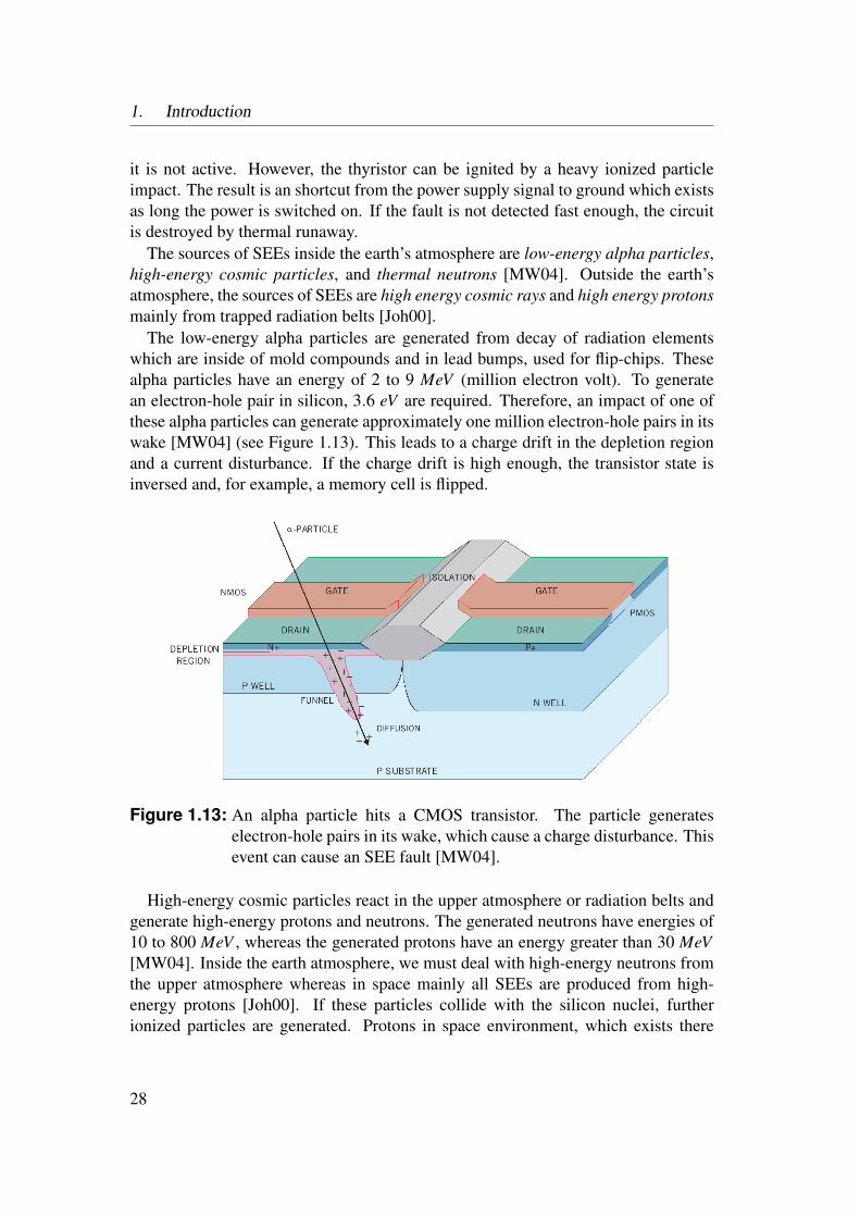
The low-energy alpha particles are generated from decay of radiation elementswhich are inside of mold compounds and in lead bumps, used for flip-chips. Thesealpha particles have an energy of 2 to 9 MeV (million electron volt). To generatean electron-hole pair in silicon, 3.6 eV are required. Therefore, an impact of one ofthese alpha particles can generate approximately one million electron-hole pairs in itswake [MW04] (see Figure 1.13). This leads to a charge drift in the depletion regionand a current disturbance. If the charge drift is high enough, the transistor state isinversed and, for example, a memory cell is flipped.
Figure 1.13: An alpha particle hits a CMOS transistor. The particle generateselectron-hole pairs in its wake, which cause a charge disturbance. Thisevent can cause an SEE fault [MW04].
High-energy cosmic particles react in the upper atmosphere or radiation belts andgenerate high-energy protons and neutrons. The generated neutrons have energies of10 to 800 MeV , whereas the generated protons have an energy greater than 30 MeV[MW04]. Inside the earth atmosphere, we must deal with high-energy neutrons fromthe upper atmosphere whereas in space mainly all SEEs are produced from high-energy protons [Joh00]. If these particles collide with the silicon nuclei, furtherionized particles are generated. Protons in space environment, which exists there
28
1.4 Attacks on Embedded Systems
in energies below 600 MeV as well as ionized particles from silicon collisions cangenerate electron-hole pairs in the substrate. Unlike alpha particles, these ionizedparticles have usually a higher energy, which results in a higher electron-holes rate.The neutron effect depends on the altitude. In an airplane, the effect can be 100 to800 times worse than on see-level [MW04].
Thermal neutrons are low-energy particles which come from the upper atmosphereand have reached the thermal equilibrium due to the loss of their kinetic energy. Theseneutrons usually have an energy of 25 meV . If the Boron-10 isotope is present onthe chip, which appears in large quantiles in BPSG (Boron-Phosphor-Silicate-Glass)dielectric layers, these neutrons are easily fetched by the isotope. This event resultsin fission where an alpha particle and a gamma ray is generated, which might leadto the SEE. If the Boron-10 isotope is present, then this is the main cause of SEEs[MW04].
SEEs are becoming increasingly important, because of the sensitivity of integratedcircuits to radiation is increasing due to smaller structure size and decreased powersupply voltage. Both trends result in reduction at the charges stored inside a nodewhich increases the probability of the appearance of an SEE [AAN00, NX06].
1.4 Attacks on Embedded Systems
There exist two ways for categorization of attacks. The first way is to categorize at-tacks by the violated security goals. The other way is to describe how the attackis realized and which way the attacker chose to compromise the system [Rag06,RRKH04].
Using the first categorization schema, the main security goals are integrity, avail-ability, and confidentiality (see Figure 1.14 above, and Section 1.2.5). Attacks whichcompromise integrity can be further subdivided into manipulation of data, manipu-lation of software or IP cores, as well as forging of authorship. Attacks which mayparalyze a system compromise the availability. Attacks to compromise the confiden-tiality of a system can be subdivided into gathering of sensitive data like passwords,keys, program code, or IP cores, and getting access control to a system. Additionally,copyright infringement compromises the confidentiality of the author of the core.
The means used to launch the attacks or the ways how the attack is realized canbe categorized into invasive and non-invasive attacks (see Figure 1.14 below). Bothgroups can further be subdivided into logical and physical attacks [RRKH04]. Phys-ical attacks typically require relatively expensive equipment and infrastructure, espe-cially physical invasive attacks. Whereas for logical attacks, usually only a computeror the embedded system is needed.
29

1. Introduction
Inte
gri
ty
Ma
nipu
latio
n of
IP
Cor
es
Ma
nipu
latio
n of
Dat
a
Ma
nipu
latio
n of
Sof
twar
e
Fo
rged
Au
thor
ship
Ava
ilab
ility
Ove
rload
the
Sys
tem
Co
nfi
den
tial
ity
Ga
ther
ing
Se
nsiti
ve D
ata
Cop
yrig
ht I
nfri
ngem
ent
Va
nqui
sh A
cces
s C
ontr
ol
Co
de
Inje
ctio
n A
ttac
ks
Sof
twar
e P
rogr
am
Har
dwar
e IP
Cor
e
Inva
sive
Ph
ysic
al A
ttac
ks
Mic
ropr
obin
g
Rev
erse
Eng
inee
ring
Dam
agi
ng
No
n-I
nva
sive
Lo
gic
al
Att
acks
Phi
shin
g
Fo
rged
Aut
hen
ticity
Cry
pto
Wea
kn.
Att
acks
No
n-I
nva
sive
Ph
ysic
al
Att
acks
Eav
esd
ropp
ing
Sid
e-C
hann
el A
tta
cks
Cop
yin
g
Des
troy
the
Sys
tem
Invasive
Non-Invasive
Logical
Physical
Logical
Physical
Co
mp
rom
ised
Sec
uri
ty G
oal
s
Mea
ns
to la
un
ch A
ttac
ks
Figure 1.14: Attacks can be categorized with the compromised security goals or theattack goals (above) and with the means to launch the attack (below).The different means of attacks can invalidate different security goals.
30

1.4 Attacks on Embedded Systems
1.4.1 Code Injection Attacks
Code injection assaults are attacks where the code integrity of a system is compro-mised. This can be the integrity of software as well the integrity of executed bitfilesin a reconfigurable system, such as FPGAs. The goals of code injection attacks aremanifolded. The demolished integrity of further program code or sensitive data, theparalysis of the system as well as getting access to sensitive data are in the foregroundof the attacker.
Code injection attacks bring the system under the control of the attacker. Programsinserted by the attacker, may easily read or alter the sensitive data and forward thedata to interfaces where the data can be collected.
To gain control over a system, the attacker must first insert a routine, which per-forms the intended behavior, into memory. This routine may, for example, read outsecured data, deactivate security protection, open gateways for the attackers, or loadanother infiltrated code from the Internet. The malicious code can be inside the pro-cessed input data which is loaded into the memory by the processor. The second stepis bringing the processor in a state to execute the inserted attacker’s code. This canbe done by manipulation of the program flow.
One way to achieve this is by utilizing buffer overflows for smashing stacks. Mostprograms are structured into subroutines with its own local variables. These variablesand also the arguments and the return address are stored in memory segments calledstacks. The return address is usually the first on the stack and the local variablesare concatenated on the bottom. Normally, like in the C programming language,the content of array variables are written from bottom to the top, and if the range isnot checked, the return address can be overwritten (see Figure 1.15). The attackercan manipulate the input data in a way that the return address is overwritten withthe address of his malicious code. On the return, the malicious code is executed[Ale96, PB04]. Another possibility is to overwrite the frame pointer address insteadof the return address [klo99].
Heap-based buffer overflows are another class of code injection attacks. The mem-ory heap is the dynamically allocated memory, in C managed by malloc() andfree(), in C++ by new() and delete(). The heap consists of many memoryblocks which are usually chained together by a double linked list. These memoryblocks are managed by the dynamic memory allocator, which can insert, unlink ormerge blocks together. The information (pointer to the previous and next block) ofthe linked lists is stored in a header for each block.
A heap-based buffer overflow may overwrite this header information in a way thatone pointer of the double linked list points to the stack segment before the returnaddress [Rag06]. If this block is now freed by the dynamic memory allocator, theheader information of the previous and next block are updated. Because one pointerpoints to the stack segment due to the attack, the stack is updated in a way that thereturn address is overwritten with the address of a heap block, which can now be
31

1. Introduction
Return Addressa[3]a[2]a[1]a[0]
bc
main
subroutine
malicious code
Program memory Detail view: Stack
Figure 1.15: On the left side, a part of the program memory is shown. Normally,the subroutine is called and after its execution, the program counterjumps back to the main program after the call instruction. However,if the return address in the stack is overwritten by a buffer overflow ofthe vector a[] (see right side), the erroneous return destination maybecome the entry point of the malicious code (dashed line).
executed after the control flow reaches a return [Rag06, PB04]. There exist manyother different possibilities to utilize heap-based buffer overflows [Con99, Dob03].
Arc injection or return-into-libc is an attack where a system function is exploitedto spawn a new process which performs the attacker’s desired operations. The namearc injection came from the inserting a new arc (control flow transfer) into the controlflow graph (CFG) of a program. In the standard C library (libc on UNIX-based sys-tems), there exists a function called system(). This function validates a processcall given as argument and after successful validation starts its execution as a newthread. The memory location of this standard function is usually known, and there-fore also the starting address to bypass the validation of the argument. The returnpointer of the stack can now be manipulated by using a stack-based buffer overflowto jump to the desired destination in the system function to execute a malicious pro-cess. The name of the malicious process can be transferred to the system function byusing registers [PB04]. This attack is useful if the architecture or operating systemprevents the stack or heap memory area from execution.
Shacham generalized the return-into-libc attacks to show that it is possible to domalicious computation without injecting malicious code [Sha07]. The idea is thatdue to shared libraries, e.g., libc, many analyzable and attackers known instructionsnippets are in the memory. Shacham proposes that an attacker can build an arbitrary
32
1.4 Attacks on Embedded Systems
program from these snippets which can do arbitrary computation. This can be doneby analyzing, for example, the libc library for code snippets which end with a returninstruction. Moreover, Shacham shows that for the x86 architecture, it is possibleto use only parts of instructions. The return instruction of the x86 architecture isa one byte instruction encoded with 0xc3. However, other instructions which arelonger consist also of this byte value. By starting the sequence in the middle of aninstruction, the original instruction alignment is bypassed which enables the attackerthe usage of additional new instruction sequences. From these building block, theattacker can build a program by chaining these snippets together by overwriting theregister which stores the return address. This so-called return-oriented programminghas been successfully transferred to other processor architectures, e.g., SPARC. In[BRSS08], a compiler is introduced which is able to construct return-oriented exploitsfrom a general propose language. In summary, Shacham shows that preventing theinjection of code is not sufficient for preventing malicious computation.
Pointer subterfuge is an attack technique where pointer values are changed. Thereexist four varieties: function pointer clobbering, data pointer manipulation, excep-tion handler hijacking and virtual pointer smashing [PB04].
Function pointer clobbering modifies a function pointer so that the pointer directsto the malicious code. When the control flow reaches the modified function call, theattacker’s function is called and his code is executed.
Data pointer modifications can be used for arbitrary memory writes. This tech-nique can be combined with other code injection attacks to launch complex attacks.
Exception handler hijacking modifies the thread environment block (in MS Win-dows) that points to the list of registered exception handler functions. Because ofthe fact that the list is stored on the stack, the entries can be easily manipulated toutilize stack based buffer overflows. This technique can be put to work to transfer thecontrol flow to a malicious function. Within Linux, function pointers in the fnlist canbe replaced to have a similar effect.
Virtual pointer smashing replaces the virtual function table used in the C++ imple-mentation of virtual functions. The virtual function table is used in C++ at runtime toimplement dynamic dispatch. Every C++ object has a virtual pointer, which pointsto the appropriate virtual function table. By modifying the virtual pointer to direct toan attacker’s virtual function table, malicious functions can be called when the nextvirtual function is invoked.
1.4.2 Invasive Physical Attacks
Invasive physical attacks physically tamper the embedded system with special equip-ment. Trivial physical attacks only compromise the availability of the system ordamage a part or the whole system by physical destruction. Also, switching off thepower supply voltage or cutting wires belongs to these trivial attacks.
33

1. Introduction
Other invasive physical attacks aim to read out confidential data or the implemen-tation of IP cores as well as the manipulation of the circuit or data to get access tosensitive data. These attacks have in common that expensive special equipment isused. The realization of these attacks requires days or weeks in specialized labora-tories. The first step is the de-packing of the circuit chips. This is usually done withspecial acids [KK99, Hag].
After removing the packaging, the layout of the circuit can be discovered with op-tical microscopes and cameras. By removing each metal layer the complete layoutof the chip can be captured in a map [KK99]. The gathered informations of the layerreconstruction can be used for reverse engineering the circuit, which gives competi-tors the possibility to optimize their product or to obtain more information about theimplementation to launch other attacks.
Further information can be collected by micro-probing the circuit. This can bedone by manual micro-probing, where metal probes have electrical contact to signalwires on chip. This is usually done on a micro-probing workstation with an opticalmicroscope [KK99].
Due to the decreased lateral structure dimensions in todays circuit technologies,manual micro-probing is nearly impossible. But there exist advanced technologies,like ion or electron beams, as well as infrared laser which make micro-probing alsopossible in todays chip manufacturing technologies. With a focused ion beam (FIB)the chip structure can be scanned in a very high resolution. The beam hits the chipsurface where electrons and ions are sputtered off and can be detected by a mass spec-trometer [DMW98]. With increased beam intensity, the beam can also remove chipmaterial with high resolution (see Figure 1.16). This can be used to cut signal wiresor drill holes to reach signal wires in underlying layers. These holes can be filled withplatinum to bring the signal to the surface, where it can be easily micro-probed. Withan electron beam tester, the activity on the signal wires can be recorded, if the clockfrequency is drastically reduced (under 100 kHz). Finally, with the infrared laser,the chip can be scanned from rear, because the silicon substrate is transparent in theinfrared wavelength range. With the photon current, internal states of transistors oractivity on signal wires can be read out [AK96, Ajl95].
These advanced technologies can be used to launch a variety of attacks. In focusare smart cards with implemented cryptographic algorithms. Most of the time, it isthe attackers goal to read a secret key. One example is to read out the memory contentusing bus probing. The problem here is the generation of the successive addressesto get a linear memory trace. The attacker can bypass the software by destroyingand deactivating the transistor gates which are responsible for branches and jumpswith an FIB. The result is a program counter with can only linearly count up, whichfits perfectly for this attack [KK99]. Other attacks are reading ROM, reviving andusing test modes, ROM overwriting by using a laser cutter, EEPROM overwriting,key retrieval using gate destruction, memory remanence, or probing single bus bits,as well as EEPROM alternation [KK99, Hag].
34
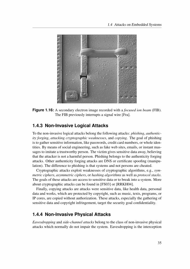
1.4 Attacks on Embedded Systems
Figure 1.16: A secondary electron image recorded with a focused ion beam (FIB).The FIB previously interrupts a signal wire [Fra].
1.4.3 Non-Invasive Logical Attacks
To the non-invasive logical attacks belong the following attacks: phishing, authentic-ity forging, attacking cryptographic weaknesses, and copying. The goal of phishingis to gather sensitive information, like passwords, credit card numbers, or whole iden-tities. By means of social engineering, such as fake web sites, emails, or instant mas-sages to imitate a trustworthy person. The victim gives sensitive data away, believingthat the attacker is not a harmful person. Phishing belongs to the authenticity forgingattacks. Other authenticity forging attacks are DNS or certificate spoofing (manipu-lation). The difference to phishing is that systems and not persons are cheated.
Cryptographic attacks exploit weaknesses of cryptographic algorithms, e.g., sym-metric ciphers, asymmetric ciphers, or hashing algorithms as well as protocol stacks.The goals of these attacks are access to sensitive data or to break into a system. Moreabout cryptographic attacks can be found in [FS03] or [RRKH04].
Finally, copying attacks are attacks were sensitive data, like health data, personaldata and works, which are protected by copyright, such as music, texts, programs, orIP cores, are copied without authorization. These attacks, especially the gathering ofsensitive data and copyright infringement, target the security goal confidentiality.
1.4.4 Non-Invasive Physical Attacks
Eavesdropping and side-channel attacks belong to the class of non-invasive physicalattacks which normally do not impair the system. Eavesdropping is the interception
35
1. Introduction
of conversations or data transmissions by unintended recipients. The attacker cangather sensitive information which is transmitted using electric media, e.g., email,instant messenger, or telephone. Sometimes a combination of eavesdropping andcryptographic weakness attacks are used to monitor sensitive data. For example,sniffing passwords in a WEP (Wired Equivalent Privacy) encrypted WLAN (WirelessLocal Area Network).
Information of cryptographic operations in embedded systems can be gathered byside-channel attacks. Usually, the goal is to get the secret key or information aboutthe implementation of the cryptographic algorithm. Cryptographic embedded sys-tems are particularly vulnerable to these attacks, because the attacker has full controlover the power and clock supply lines. The different side-channel attacks are timinganalysis, power analysis, electromagnetic analysis, fault analysis, and glitch analysis[Hag, KLMR04, RRKH04].
Timing analysis attacks are based on the correlation of output data timing behav-ior and internal data values. Kocher [Koc96] showed that it is possible to determinesecret keys by analyzing small variations in the execution time of cryptographic com-putations. Different key bit values cause different execution time, which makes a readout and reconstruction of the key possible.
Power analysis attacks are based on the fact that different instructions cause varia-tions in the activities on the signal lines, which result in different power consumption.The power consumption can be easily measured by observing the current or the volt-age on a shunt resistor. With simple power analysis (SPA) [KJJ99], the measuredpower consumption is directly interpreted to the different operations in a crypto-graphic algorithm. With this technique, program parts in a microprocessor, for ex-ample DES rounds or RSA operations, can be identified. Because of the executionof these program parts depend on a key bit, the key bits can be read out. Differentialpower analysis (DPA) [KJJ99] is an enhanced method which uses statistical analy-sis, error correction and correlation techniques to extract exact information about thesecret key.
Similar to power analysis techniques, information about the key, data, or the cryp-tographic algorithm or implementation can be extracted by electromagnetic radiationanalysis [AARR03].
During different fault analysis (DFA) attacks, the system is exposed to harsh en-vironment conditions, like heat, vibrations, pressure, or radiation, to enforce faultswhich result in an erroneous output. Comparing this output to the correct one, the an-alyst gains insight into the implementation of the cryptographic algorithms as well asthe secret key. With DFA attacks, it was possible to extract the key from a DES imple-mentation [BS97] as well as public key algorithm implementations [BDH+98, BS97].The last one shows that a single bit fault can cause fatal leakage of information whichcan be used to extract the key. Pellegrini and others show that using fault analysis,where the supply voltage of an processor is lowered, it is possible to reconstruct sev-eral bits from a secret key of the RSA cryptographic algorithm [PBA10]. For this
36

1.5 Contributions
attack, they used the RSA implementation of the common OpenSSL cryptographiclibrary and a SPARC Leon3 core, implemented on a Xilinx Virtex-II Pro FPGA. Thesupply voltage of the FPGA is lowered till sporadic bit errors occur on the calculationof the signature using the FPGA’s hardcore multiplier.
Glitch attacks also belong to the class of DFA attacks. Here, additional glitchesare inserted into the clock signal to prevent the registering of signal values on thecritical path. The simplest attack is to increase the clock frequency. One goal of glitchattacks can be the prevention of branches in a microprocessor program, because of thecalculation and registering of the new branch target address is a long combinatorialpath on many processor implementations [KK99].
1.5 Contributions
It has been shown in the previous sections of this chapter that security and reliabilityin embedded systems are very important topics, and that their significance is likelyto increase in the future. Additionally, this and the next chapter show that the topicinvolves a wide research area with a large number of annual publications. Afterthis introduction, major contributions of this thesis with respect to these topics areoutlined, concentrating on two major concerns, namely:
• Identification and Watermarking of IP Cores and
• Control Flow Checking.
The first topic is mainly about security issues, and is concerned with countermea-sures against unauthorized copying of IP cores, which compromises the confidential-ity of the core’s author. The second topic mainly treats reliability issues, but alsosecurity issues. In particular, soft errors (see Section 1.3.4), but also some degen-eration faults (see Section 1.3.1) and code injection attacks (see Section 1.4.1) arediscussed. Physical attacks, which affect the control flow of a program running onan embedded system (see Section 1.4.2 invasive physical attacks and Section 1.4.4differential fault analysis), are focused on as well. The key scientific contributions ofthis dissertation are summarized as follows:
• Watermarking and Identification Techniques for FPGA IP Cores: Unlikemost existing watermarking techniques, the focus of our techniques lies onease of verification, even if the protected cores are embedded into a product.Moreover, we have concentrated on higher abstraction levels for embeddingthe watermark, particularly at the logic level, where IP cores are distributed asnetlist cores. With the presented watermarking methods, it is possible to wa-termark IP cores at the logic level and identify them with a high likelihood andin a reproducible way in a purchased product from a company that is suspected
37
1. Introduction
to have committed IP fraud. To the best of our knowledge, this is only possiblefor netlist cores using our watermarking techniques. Moreover, approaches toidentify an embedded core by looking at special core properties without usinga watermark are presented as well [ZAT06]. Using these techniques, we coverthe protection of IP cores on all different abstraction levels from RTL to devicelevel without restrictions on the verifiability in a given product.
The investigated techniques establish the authorship by verification of either anFPGA bitfile (see also [ZAT06, SZT08]) or the power consumption of a givenFPGA (see also [ZT06, ZT08b, ZBT10b, ZT07a, ZT07b]). Both the FPGAbitfile and the measurement of the power consumption can be easily obtainedfrom a given product. However, if the product vendor uses encrypted bitfiles,only the watermark verification using the power consumption is possible withthe proposed methods. On the other hand, if the FPGA embeds multiple wa-termarked cores, the different power watermarking signals superpose whichmakes extraction of watermarks harder or even impossible. To circumvent thisobstacle, we propose multiplexing methods [ZBT10a]. Furthermore, we wouldlike to remark that the proposed power watermarking technique, which is theonly watermark verification method for netlist cores and the first one availablefor bitfile cores which works with bitfile encryption. Another watermarkingtechnique for encrypted bitfiles, introduced in [KMM08], uses thermal dissi-pation for verification and is commercially available as the product DesignTagfrom Algotonix. The commercialization underlines that there is a real demandfor IP protection by such watermarking techniques.
In summary, the key contributions of this part of the dissertation are:
– Extended theoretical watermarking and identificationmodels
– Non-invasive verification using solely the given product– Watermarking and identification of IP cores published as
HDL, netlist, and bitfile cores– Identification and watermarking techniques using the bit-
file for verification– Novel watermark verification techniques based on the ex-
ploration of power consumption
• Control Flow Checking for Embedded RISC Processors and General IPCores: The goal of control flow checking is to recognize, analyze, and correctsporadic and/or permanent errors that occur in the control path of embeddedCPUs or IP cores. Our vision is to define autonomously behaving elements[SBE+07b, SBE+07a] that resolve functional errors of the control paths locally
38
1.5 Contributions
inside the core at runtime and prevent false instructions or transitions frombeing executed, which could lead to an erroneous state (error-resilience). Thecorresponding autonomous elements are called control flow checkers. They aresupposed to recognize, evaluate, and even correct errors during runtime whichaffects the control flow of an embedded CPU or IP core (see also [ZT08a,ZT09]).
We present techniques for fast error detection inside embedded processors,which is important because errors should be detected even before they can man-ifest into registers or memories. This is achieved by monitoring the control flowin the first pipeline stages of the processors which makes it possible to correcterrors by a simple re-execution of the erroneous instructions without time andarea expensive restoration of registers and memory states. This allows us tobuild a lightweight checker unit with very low area and only moderate memoryoverhead.
Proposed is a unique control flow checking framework based on a modular ap-proach. Modularity allows to add or remove features in order to reduce theoverhead, to increase the error coverage, or add error correction measures. Us-ing our control flow checking approach, the developer of a core is able to decideabout trade offs between different features and their respective overheads.
Moreover, we point out the possibility of fast error correction and the integra-tion of these techniques with the methods for data path protection. This com-bination with data path protection scheme introduced in [BZS+06] enables anembedded RISC processor to detect disturbances, originating from the under-lying semiconductor technology as, for example, single event effects, and toreact accordingly. Both aspects, the fast error correction and the combinationwith data path protection, are new and go beyond the state-of-the-art of existingcontrol flow checking techniques. Other benefits of this approach are that it isnot necessary to change the application code or insert any additional instruc-tions. Therefore, there is no performance impact on error-free execution. Theapproach can be easily integrated into the software development flow and thus,the presented technique is completely transparent to the program developer.
This work provides new control flow methods mainly for embedded RISC-CPUs, which are also applicable for general IP cores. The focus in this contextis put on methods that can be easily integrated into ASIC designs. Naturally,these methods can also be used in FPGA designs, however the necessary reli-able underlying FPGA structure is not part of this work.
In summary, the key contributions of this part of the dissertation are:
– New methods for lightweight control flow checking– Detection of all errors which affect the control flow
39
1. Introduction
– Control flow checking techniques for embedded RISCCPUs and general IP cores using programmable hardwarechecker units
– Modular approach with support for fast error detection andcorrection and low hardware overhead
– Support of direct and indirect control flow instructions– Integration with methods for data path protection for em-
bedded CPUs– Prototypical implementation for the SPARC Leon3 proces-
sor
Both topics address problems which have a high significance for embedded sys-tems today and the importance tends to rise in the future with the ongoing technologyimprovements and the integration of more and more cores to very complex systems-on-a-chip. In particular, IP core watermarking addresses the issue of copyright pro-tection in an increasing market of IP cores, whilst control flow checking addressesproblems including soft errors, even in combinatorial logic in with the occurrence ofsoft errors is a new challenge.
On the other hand, hardware overhead and easy integration into processor designand application development flows are of utmost importance in many cost-sensitivesystems, particularly in embedded systems. Both methodologies, watermarking andcontrol flow checking, have a relatively low hardware overhead and are easy to inte-grate into current design flows. From the design flow point of view, this is an evo-lution, not a revolution, which means that today’s design tools can be used furtheronand without compromise.
Finally, this work provides case studies for FPGA implementations and experimen-tal evaluations. Besides the demonstration of feasibility of the proposed methods,these case studies indicate the amount of overhead for an FPGA implementation.
1.5.1 Overview of the Thesis
The remainder of this thesis is organized as follows:Chapter 2 gives an overview of related work for security and reliability in em-
bedded systems. The focus lies on methods for watermarking and IP protection ofIP cores, defenses against code injection attacks, measures against faults and errors,as well as methods for control flow checking in embedded CPUs and general RISCcores.
Chapter 3 provides new methods for IP core watermarking and identification.After introducing a novel theoretical model for watermarking and the threats to it,methods for bitfile and power watermarking are presented. The bitfile watermarking
40

1.5 Contributions
section presents methods using the lookup table content to identify the core (also pre-sented in [ZAT06]), as well as an implementation of watermarking using functionallookup tables (also presented in [SZT08]). The next section treats power watermark-ing. First, the model of the communication channel is introduced and then the ba-sic power watermarking methods. After that, several new methods which increasethe decoding robustness are presented (partly also presented in [ZT06], [ZT08b],[ZBT10b], [ZBT10a], [ZT07a], and [ZT07b]). Finally, experimental results for thebitfile and power watermarking are given.
Chapter 4 deals with techniques for control flow checking. The focus lies onmethods checking the correctness of control flow instructions issued during the ex-ecution of programs for embedded RISC CPUs. Using the suggested methodology,any error of illegal or faulty direct or indirect jump and branch instruction can bedetected for a given program code at runtime. Moreover, techniques for checkingthe control flow of general IP cores are presented. Furthermore, hardware conceptsfor a generic modular control flow checking framework which may be tightly at-tached to a given CPU are proposed. Finally, a prototypical implementation for theSPARC Leon3 processor and a case study which implements a turbo encoding/de-coding system, also presented in [MWB+10], are shown. Most of the control flowchecking methodology for embedded RISC processors is also presented in [ZT08a]and [ZT09].
Chapter 5 concludes the work and gives an outlook for future work.
41

1. Introduction
42
2Related Work
This chapter provides an overview of related work on security and reliability of em-bedded systems. Because of this is a very vast topic, we concentrate on issues relatedto IP core protection as well as control flow checking for embedded CPUs and IPcores.
The chapter is structured as follows: First, methods which increase the securityof embedded systems are discussed. This includes methods for IP protection relatedto IP core watermarking and identification as well as measures against code injec-tion attacks, related to control flow checking. Second, methods which increase thereliability of embedded systems are discussed. In focus are measures against singleevent effects and degeneration faults. Finally, approaches for control flow checkingare presented.
2.1 Security: IP Protection
Intellectual property (IP) denotes the absolute right on an intangible asset, like music,literature, artistic works, discoveries, inventions, words, phrases, symbols, designs,software, or IP cores. The owner of the IP can license his work to other peopleor companies. IPs are protected by law with patents, copyrights, trademarks, andindustrial design rights.
Drimer defines the following protection or defense categories against IP theft orfraud [Dri09]: social, reactive, and active protections.
Social protection means that IP works are protected by laws, non-disclosure agree-ments, copyrights, trademarks, patents, contracts, and so on. The deterrents are con-
43

2. Related Work
viction by a court of law and the loss of a good reputation. However, these deterrentsare only effective if the misconduct can be proven and the appropriate laws exist.Furthermore, the laws must be enforced which is handled differently from country tocountry.
Reactive protection means that the theft or fraud cannot be prevented, however, itcan be detected and delivers evidence of the misconduct. Some reactive protectionmechanisms deliver only suspicious facts which, however, may be enough to triggerfurther investigations. Furthermore, the persistence of reactive protection mecha-nisms might deter would-be attackers.
Active protection means that physical or cryptographic mechanisms prevent thetheft or fraudulent usage of the protected work. This category has the highest deter-rent degree. However, these mechanisms can be broken by attacks. Often the attackcan be proven if the misconduct is detected.
In this work, we concentrate on the protection of the IP of hardware cores. Theseso called IP cores are distributed like software and can easily be copied. Some coresuppliers encrypt their cores and deliver special development tools which can handleencrypted cores. The disadvantage is that common tools cannot handle encryptedcores and that the shipped tools can be cracked so that unlicensed cores can be pro-cessed. Another approach is to hide a signature in the core, a so-called watermark,which can be used as a reactive proof of the original ownership. There exist manyconcepts and approaches on the issue of integrating a watermark into a core.
In general, hiding a unique signature into user data, such as pictures, video, au-dio, text, program code, or IP cores is called watermarking. Embedding a watermarkinto multimedia data is achieved by altering the data slightly at points where humansense organs have lower perception sensitivity. For example, one can remove fre-quencies which cannot be perceived by the human ear by coding an audio sequenceinto an MP3 file. Now, it is possible to hide a signature into these frequencies withoutdecreasing quality of the coded audio sequence [BTH96].
One problem of watermarking is that for verification, the existence and the charac-teristic of a watermark must be disclosed, which enables possible attackers to removethe watermark. To overcome this obstacle, Adelsbach and others [ARS04] and Li andothers [LC06] presented so-called zero-knowledge watermark schemes which enablethe detection of the watermark without disclosing relevant information.
The watermarking of IP cores is different from multimedia watermarking, becausethe user data, which represents the circuit, must not be altered since functional cor-rectness must be preserved. A fingerprint denotes a watermark which is varied forindividual copies of a core. This technique can be used to identify individual autho-rized users. In case of an unauthorized copy, the user, the copied source belongs to,can be detected and the copyright infringement may be reconstructed. Watermark-ing procedures can be categorized into two groups of methods: additive methods andconstraint-based methods.
44
2.1 Security: IP Protection
In additive methods, the signature is added to the functional core, for example, byusing unused lookup-tables in an FPGA [LMSP98]. The constraint-based methodswere originally introduced by [KLMS+01] and restrict the solution space of an op-timization algorithm by setting additional constraints which are used to encode thesignature.
A survey and analysis of watermarking techniques in the context of IP cores isprovided by Abdel-Hamid and others [AHTA04]. Further, we refer to our own surveyof watermarking techniques for FPGA designs [ZT05]. A survey of security topicsfor FPGAs is given by Drimer [Dri09] who also maintains the FPGA design securitybibliography website: http://www.cl.cam.ac.uk/˜sd410/fpgasec/.
In order to compare different watermarking strategies, some criteria are defined inthe following [HP99]:
Functional correctness: This is the most important criteria. If the watermarkprocess destroys the functional correctness, it is useless to distribute the core.
Resource overhead: Many watermarking techniques need some extra resources.Some to generate and store the watermark itself, some because of the degradation ofthe optimization results from the design tools. The ratio between the original and thewatermarked core’s resource demand is defined as the resource overhead.
Transparency: The watermark procedure should be transparent to the designtools. It should be easy to integrate the watermarking step into the design flow, with-out altering common design tools.
Verifiability: The watermark should be embedded in such a way that the author-ship can be verified easily. It should be possible to read out the watermark only withthe given product and without any further information from the design flow whichmust be requested from a company suspected of IP fraud.
Difficulty of removal: The watermark should be resistant against removal. Theeffort to remove the watermark should be greater than the effort needed to develop anew core, or the removal of the watermark should cause corruptness of the function-ality of the core. Watermarks which are embedded into the function of the core arein general more robust against removal than additive watermarks.
Strong proof of authorship: The watermark should identify the author with astrong proof. It should be impossible that other persons can claim the ownership ofthe core. The watermarking procedure must be resistant against tampering.
45

2. Related Work
In this section, we first discuss IP protection methods using core encryption. Af-ter that, related work using additive and constraint based watermarking methods ispresented.
2.1.1 Encryption of IP Cores
The goals of active IP protection for cores are, first, that the core cannot be usedwithout a proper license and, second, that the core is protected from unauthorizedmodifications. The cores can be delivered in encrypted form and are decrypted bydesign tools. Other approaches for FPGAs use an encrypted configuration bitfilewhich is decrypted on the FPGA.
Encrypted HDL or Netlist Cores
One solution is to deliver encrypted IP cores to the customers and integrate de- andencryption functions into the EDA tools. The customer buys the encrypted core andobtains the appropriate key from the IP core developer or vendor. This technique isapplicable for IP cores of all abstraction or technology levels (RTL – HDL cores,logic level – netlist cores, device level – bitfile/layout cores). However, if, e.g., anHDL core should be protected at all abstraction levels, the synthesis tool must pro-duce an encrypted netlist. This must be done for all steps: decryption of the core,processing, and encryption. It is important that the customer only has access to theencrypted data, which means that the EDA tool routines must be protected againstread out attacks.
The problem is that no consistent industrial standard exists which handles en-crypted IP cores [Dau06]. This complicates the interoperability of IP cores and EDAtools.
Today, symmetric and asymmetric cryptographic approaches are used. Using sym-metric cryptographic approaches, the en- and decryption is done with the same key.The advantage of this approach is the reduced computational complexity comparedto asymmetric approaches. One problem is the secure distribution and communica-tion of the key. Furthermore, EDA tools must deal with different keys for differentIP vendors, and if one key is cracked, usually all IP cores of the corresponding ven-dor have lost their protection. Nevertheless, this approach is used, for example, byXilinx to encrypt some of their parameterizable HDL IP cores, e.g., the Microblazeprocessor softcore [Xild].
Methods using asymmetric cryptography are also known as public key cryptog-raphy which need two keys, the private and the public key. The private key is fordecryption inside the EDA tools, where as the encryption key is publicly availableand is used by the IP core vendor. The EDA vendor creates the key pairs and embedsthe private key in his tools. The IP core developer can now use the public key for theencryption. The advantage is that the private decryption key may not be transferred
46
2.1 Security: IP Protection
over untrusted communication channels and is only known by the EDA vendor. Thedisadvantage is that asymmetric approaches have a high computational complexitywhich results in long runtime for decryption up to several hours for IP cores [Dau06].Another drawback is that the IP vendor must create a separate version for each EDAtool, which is encrypted with the corresponding public key of the EDA vendor.
Dauman, Vice President of the Synopsys’ Synplicity Business Group, introduced ahybrid approach [Dau06]. The IP core is encrypted with a symmetric cryptographicmethod, like Triple-DES, or AES using a key which is generated by the IP vendor.This key, now referenced as the data key, is encrypted with an asymmetric crypto-graphic method, like RSA [RSA78], with the public key of the EDA vendor. Thisapproach is similar to the PGP approach [Zim95] for cryptographic privacy and au-thentication of messages. The decryption is done with the (decrypted) data key andthe cryptographic method which is specified by the IP vendor. Inside the EDA tools,there exist different symmetric cryptographic routines for the decryption of the core.The advantage is that the decryption with a symmetric algorithm is very fast and thecomputational complex asymmetric method is only used for the data key which isvery small compared to the whole IP core. Synplicity suggested this approach asfuture industry standard and includes this method called ReadyIP into the productSynplify Premier [Syna].
In 2007, a industry-wide panel discussion [Wil07] provided some insight into theperception of encrypted IP cores of the EDA industry. The conclusion was that thecurrent social-based protection works well for large cooperations. A better solutionis desirable but not necessarily urgent. However, they express their reservation tosmall companies or startups which are not known in the community and might not bewilling to sell IP cores to these companies.
Barrick argued against the usage of encrypted netlist cores due to their hiddencosts [Bar]. The disadvantages are the fixed constraints, the prevention to reuse partsof the logic for other cores, slower simulation speed or inaccurate behavioral models,restriction of the choice of EDA tools, and fewer debugging possibilities. However,sometimes encryption can be worth due to reduced acquisition costs.
Encrypted FPGA Configurations
Another kind of IP protection is the encryption of the FPGA configuration or bitfile.The bitfile is stored in a non-volatile memory, e.g., a PROM, and transferred to theFPGA encrypted. Inside the FPGA during the configuration, the bitfile is decrypted.This approach prevents copy attacks for bitfile designs and protects the bitfile fromreverse engineering.
The first suggestion of this method was in 1995 by a patent from Austin [Aus95].The first FPGA devices which offered configuration encryption was the Actel’s 60RSfamily. However, all FPGAs had the same permanent key, which prevents no copy at-tacks. Furthermore, the key was also stored in the software. Consequently, it was easy
47
2. Related Work
for attackers to extract the key from the software. Xilinx introduced configuration de-cryption with a Triple-DES hardcore for Virtex-II devices in the year 2000. The userdefined key can be stored and updated into an FPGA internal battery-backed SRAM.Today, bitfile encryption is supported by many high-end FPGA families. Some FPGAdevices, such as the Altera Stratix II/III, can be configured to always perform decryp-tion. This prevents the configuration with bitfiles which are not encrypted with theproper key.
There exist two different key storing techniques: volatile and non-volatile. Volatilekey storing uses low power SRAMs which are powered by an external battery. At-tackers must keep powering the key storage during the attack, which is more com-plicated. On an attacker’s error, the key is cleared and the bitfile cannot be loaded.The disadvantage is the increased printed circuit board space and costs for the exter-nal battery. Non-volatile key storage uses fuses, flash, or EEPROMs. The problemis that these technologies must be combined with the latest CMOS technology onthe same chip, which affords in a non-standard manufacturing step. The results areincreasing costs and more complex verification strategies.
An important aspect of methods using encrypted FPGA configuration bitfiles is thekey management which includes the generation and the distribution of keys. Keansuggests a method where the FPGA can encrypt and decrypt bitfiles with hardwarecores and a permanent embedded key [Kea01]. The FPGA is able to encrypt the bitfileon the first programming and store this encrypted bitfile in a non-volatile memory.Upon every FPGA configuration during the power-up cycle, the bitfile is loaded anddecrypted in the FPGA. The advantage is that the key never leaves the FPGA.
Bosset and others [BGB06] propose a method for using partial reconfiguration foren- and decryption of FPGA bitfiles by user-defined soft cores. At power-up, thedecryption core is initially loaded form the PROM which decrypts the bitfile with theuser logic. Soudan and others [SAH] propose a method for the encryption of partiallyreconfigurable bitfiles using device-specific keys.
2.1.2 Additive Watermarking of IP Cores
Additive methods are watermarking procedures, where a signature is added to thecore. This means that the watermark is not embedded into the function of the core.Nevertheless, the watermark can be masked, so it appears to be part of the functionalpart. Additive watermarks can be embedded into HDL, netlist, bitfile or layout cores.
HDL Cores
Additive watermarking for HDL cores seems to be very complicated, because of thehuman-readable structure of the HDL code. Hiding a watermark there is very dif-ficult, because on the one hand, an attacker may easily detect the watermark, and
48

2.1 Security: IP Protection
on the other hand, subsequently used design tools might remove the watermark dur-ing circuit optimization. However, it is not impossible to include an additive HDLcomponent into the core, which may not removed by the design tools.
Castillo and others hide a signature into unused space of dedicated lookup tablebased memory [CPG+06]. To extract the signature, an additional logic monitors theinput stream for a special signature extraction sequence. If this sequence is detected,the signature is sent to the outputs of the core. This approach was later generalizedfor other memory structures in [CPG+08]. The drawback is that distribution as anHDL core is not possible, because the signature extracting logic is easy to detect andto remove.
Oliveira presents a general method for watermarking finite state machines (FSMs)in a way that on occurrence of a certain input sequence, a specific property exhibits[Oli01]. The certain input sequence corresponds to the signature which is previouslyprocessed by cryptographic functions. A similar approach is presented by Torunogluand others in [TC00] which explores unused transitions.
Fan provides a method where the watermark or signature is sent as a preamble ofthe output of the test mode [FT03]. Some ASIC circuits provide a special test modewhich stimulates the core with special input patterns. To analyze the correctness ofthe core, the output of these input patterns are measured and compared to the correctpatterns. The idea is to send the watermark sequence over the output port before thetest sequence starts.
The disadvantage of these approaches is the usage of ports for signature verifica-tion. This works only if the ports are reachable. If the core is embedded into othercores, the ports of the watermarked core can be altered which falsifies or preventsthe detection of the signature in the output stream. This applies also to the signatureextraction sequence in the input stream.
Netlist Cores
To the best of our knowledge, there exist no publications on the use of additive wa-termarking at the level of netlist cores. In [ZT05] we presented the first two examplesof how additional watermarking for netlist cores can look like. The first idea is to ap-ply redundant logic in some paths of the core according to a signature. To verify thewatermark, one can optimize the core so that the redundant logic is removed, showthe differences and reconstruct the signature.
The second idea is to add false paths in the design which do not affect the followinglogic. The weakness of both ideas is that the design tools applied in subsequent stepsuse transformations which may destroy the watermark. Therefore, these ideas are notapplicable.
49
2. Related Work
Bitfile Cores
The approach of Lach and others watermarks bitfile cores by encoding the signa-ture into unused lookup tables [LMSP98]. At first, the signature will be hashed andcoded with an error correction code (ECC) to be able to reconstruct the signatureeven if some lookup tables are lost, e.g., during tampering. After the initial place androute pass, the number of unused lookup tables will be determined. The signature issplit into the size of the lookup tables and additional LUTs are added to the design.Then, the place and route process will be started again with the watermarked design.Later, the approach was improved by using many small watermarks instead of a sin-gle large one [LMSP99]. The size of the watermarks should be limited by the size ofa lookup table. The advantage is that small watermarks are easier to search for, andfor verification, only a part of all of watermark positions must be published. Withthe knowledge of the published position, the watermark can be easily removed byan attacker. At the verification process, only a few positions of the watermark needto be used to establish the ownership. A second improvement is that a fingerprintingtechnology is added to the approach that enables the owner to see which customer hasgiven the core away [LMSP01]. The fingerprinting technology is achieved by divid-ing the FPGA into tiles. In each tile, one lookup table is reserved for the watermark.The position of the mark in the tile encodes the fingerprint. For verification, it ispossible to read out the content of the lookup table from a bitfile. So, these methodsare easy to verify. It’s more difficult to determine the position of the watermark in atile, but it’s still generally possible. However, if an attacker knows the position of thewatermark, it is easy to overwrite it.
Saha and others present a watermarking strategy for FPGA bitfiles by subdividingthe lookup table locations into sets of 2× 2 tiles [SSK07]. The number of usedlookup tables in a set is used as signature. From an initial level, additional lookuptables are added to achieve the fill level according to the signature. The input andoutput are connected to the don’t care inputs of the neighboring cells. Kahng andothers show in [KLMS+98] that the configuration of the multiplexer of unused CLBoutputs in FPGA bitfiles can carry a signature. The signature is embedded after thebitfile creation and by knowing the encoding of the bitfile. These configuration bitscan be later extracted to verify the signature.
Van Le and Desmedt show that these additional watermark schemes for bitfilecores can be easily attacked by reverse engineering, watermark localization, and sub-sequent watermark removal [LD03]. A simple algorithm is introduced which iden-tifies lookup tables or multiplexers whose outputs are not connected to any outputpins. However, these attacks are only successful if reverse engineering of the bitfileis possible and the costs of reverse engineering are not too high. More about attackingcosts is described in Section 3.2.
Finally, Kean and others present a watermarking strategy where a signature is em-bedded into an FPGA bitfile core or design [KMM08]. The read out of the signature
50
2.1 Security: IP Protection
is done by measuring the temperature of the FPGA. This approach is commerciallyavailable as the product DesignTag from Algotronix.
2.1.3 Constraint-Based Watermarking of IP CoresAll optimization problems have constraints which must be satisfied to achieve a validsolution. Solutions which satisfy this constraints are the solution space. Constraint-based watermarking techniques represent a signature as a set of additional constraintswhich are applied to the hardware optimization and synthesis problem. These addi-tional constraints reduce the solution space (see Figure 2.1) since the chosen solutionmust also satisfy the additional constraints. The same solution could be achievedwith neglecting these additional constraints with probability Pc. The probability Pc ofthis event is given by the following formula:
Pc =nw
no(2.1)
where no is the number of solutions which satisfy the original constraints and nw isthe number of solutions which satisfy both the original and the additional constraints[KLMS+01, KHPC98]. If Pc is very small, a solution that also satisfies the additional(watermarking) constraints is a strong proof of the existence of the watermark.
valid optimization solutions
solution space for the watermarked design
Figure 2.1: The solution space of an original and a watermarked design. If a de-sign satisfies the original and the additional constraints, then the designis protected by a watermark. The probability that the additional con-straints are satisfied by chance should be low to have a strong proof ofauthorship.
Qu proposes a methodology to make a part of the watermark – for constraint-based watermarking, some additional constraints – public which should deter attack-ers [Qu02]. The other parts, called private watermark, are only known by the coreauthor and are used to verify the authorship in case that the public watermark was at-tacked. A similar approach is used by Qu and others to generate different fingerprints
51

2. Related Work
by dividing the additional constraints into two parts [QP00]: The first part is a set ofrelaxed constraints which denote the watermark. By applying distinct constraints tothe second part, different independent solutions can be generated which may be usedas diverse fingerprinted designs.
Charbon proposed a technique to embed watermarks on different abstraction levelswhich he called hierarchical watermarking [Cha98]. The idea is, if an attacker isable to remove a watermark, for example, embedded into the layout of a circuit, thewatermarks added at higher abstraction levels are still present. However, Charbonfocused more on layout, nets, and latch watermarking techniques which are onlyapplicable for ASIC layout cores.
The verification of a constraint-based watermark is usually done with the water-marked core as it is. This means the watermarked core can be purchased or publishedand from the distributed cores the watermark can be verified. However, if the coreis combined with other cores and traverses further design steps, the watermark infor-mation is usually lost or it cannot be extracted.
Van Le and Desmedt [LD03] present an ambiguous attack (see Section 3.2) forconstraint-based watermarking techniques. The authors add further constraints tothe watermarked solution by allowing only a minimal increase of the overhead. Theresult is a slightly degenerated solution which satisfies many additional constraints.This means that in this solution, a lot of different signatures can be found whichdestroys the unique identification of the core developer. They choose, for example,the constraint-based watermarking approach for graph coloring. Further, this attackmight be applicable to other constraint-based watermarking techniques.
As it was the case with additive watermarking strategies, constraint-based water-marking strategies are applicable for HDL, netlist, and bitfile cores.
HDL Cores
HDL code is usually produced by human developers or high-level synthesis tools.Both can set additional constraints to watermark a design. One approach is to use awatermarked scan chain [KP98]. Scan chains are usually used in ASIC designs toaccess the internal registers for debugging purposes. The use of scan chains in FPGAdesigns is rather unusual, but might be helpful in some cases. At first, a number willbe assigned to each register, and the registers will be sorted. Now, a pseudo randomsequence will be generated from the signature (one example is given in Section 3.2.2).Registers are selected with an algorithm which uses a random sequence as input. ForKc scan chains, the first Kc selected registers are chosen as the first register in eachchain. Depending on the signature, we have a variation on the scan chains whichcan be used to detect the watermark. It is possible that an unfortunately chosen startof a chain could result in the allocation of more routing resources. Moreover, themaximum clock frequency for the scan chain can be limited. This approach is easy toverify, if the scan chains can be accessed from outside of the chip. Problems occur,
52

2.1 Security: IP Protection
if the scan chain is only used internally or is not connected to any device. In such acase, there is no verification possibility.
Some work was done for watermarking digital signal processing (DSP) functions[RAMSP99, CD00]. This kind of watermarking has more in common with media wa-termarking instead if IP watermarking. Both approaches alter the function of the coreslightly by embedding a watermark. In [RAMSP99], the coefficients of finite impulseresponse (FIR) filters are slightly varied according to the watermark. Additionally,the authors use different structures to build the FIR filter which also corresponds tothe signature. In [CD00], these ideas are extended and proven correct by mathemati-cal analysis.
Netlist Cores
An approach to watermark netlist cores is to preserve certain nets during synthesis andmapping [KHPC98]. Synthesis tools merge signals or nets together and produce newnets. Only a few nets from the synthesis input will be visible in the synthesis result.The technology mapping tool also eliminates nets by assembling gates together in alookup table. Kirovski’s approach enumerates and sorts all nets in a design. The firstKc (see previous section) nets of the input are chosen by the synthesis tools accordingto a signature. These nets will be prevented from elimination by the design toolsby connecting these nets to a temporary output of the core. The new outputs fromadditional constraints for the synthesis tool, and the corresponding result is related tothe watermark. A disadvantage is that it is easy to remove the additional logic. If thecontent of the lookup table is synthesized again, the watermark will be removed.
Meguerdichan and others presented a similar approach for netlist cores where ad-ditional constraints are added during the technology mapping step of the synthesisprocess [MP00]. In this approach, critical signals are not altered which preserves thetiming and the performance of the core. The signature is encoded into the number ofallowed inputs of a certain primitive cell, e.g., a gate or a lookup table. The primitivecells which are not in the critical path are enumerated, and according to the signature,the number of usable inputs are constrained.
Khan and others watermark netlist cores by doing a rewiring after synthesis [KT05].Rewiring means that redundant connections between primitive cells are added in thenetlist which makes other original connections redundant. These new redundant con-nections are removed.
Bai and others introduce a method for watermarking transistor netlists for full cus-tom designs [BGXC07]. The transistors are enumerated and sorted into a list like inthe approach above. Corresponding to the pseudo random stream generated from thesignature, the width of the transistor gate is altered. If the transistor is assigned a ’1’from the random stream, the transistor width is increased by a constant value.
53

2. Related Work
Bitfile and Layout Cores
Additional placement, routing, or timing constraints can be added to watermark bit-file cores. To embed a watermark with placement constraints, Kahng and others placethe configurable logic blocks (CLBs) in even or odd rows depending on the signature[KMM+98]. In this approach, the signature is transformed into even/odd row place-ment constraints. The placed core will be tested on preserving the constraints and,if necessary, CLBs are swapped. This method has no logical resource overhead andthe additional costs of routing the resources are very small or tend to zero, becausethe placement is altered only marginally. The problem of verification is to extractthe CLB placement information. Only if knowing how the CLBs correspond to thesignature, the watermark can be verified. A strategy to achieve this is to uniquelyenumerate the CLBs in an FPGA from the top left corner.
Kahng and others [KMM+98] propose a second approach by adding constraintsto the router. The constraints achieve that a net selected by the signature is routedwith some additional, unusual routing resources. These unusual resources can be, forexample, wrong way segments. A wrong way segment is a segment in which the netgoes to the wrong direction and then back in the right direction to form a backstrap.The authors claim that this is unlikely for a normal router, and so such a net can beverified as a watermarked net.
Furthermore, additional timing constraints can be used to watermark a core. Tim-ing constraints limit the route and logic delay between two registers. Kahng andothers propose a technique to select paths which have timing constraints accordingto the signature. The timing constraints for these paths are split into two separateconstraints. For example, let a path have six logic gates and a timing constraint of10 ns. The new constraint is 4 ns for the first 3 cells and 6 ns for the rest [KLMS+01].
Another approach by Jain and others measures the delay on selected paths and addsnew timing constraints on these paths [JYPQ03]. The new constraints are chosenbased on the measured delay by setting the last digit to a value of a bit from thesignature. For example, let a path have a delay of 5.73 ns. If the coded bit is a ’1’, thenew constraint for this path is 5.71 ns, if the coded bit is ’0’, the constraint is 5.70 ns.
Narayan and others present a watermarking approach of the layout by modifyingthe number of vias and bends of certain nets [NNC+01]. Like in other approaches,the nets are enumerated, and additional vias or bends are inserted according to thesignature.
Saha and others present a watermarking scheme by altering the size of the repeatersaccording to the signature [SSK07]. In high performance ASIC designs, repeaters (abuffer for amplification of the signal) are inserted into critical nets to decrease thedelay.
54

2.1 Security: IP Protection
2.1.4 Other Approaches
Many other approaches exist for protecting IP cores or designs from unlicensed usageor alteration. For example, the VHDL Obfuscator & Watermarker [VIS] is able toobfuscate VHDL cores in a way that the algorithm is hidden, but leaves the coresynthesizeable. This approach make reverse engineering and alteration of the coremuch harder. Further, by using different scrambling techniques, a watermark can beembedded in the obfuscated code. Clearly, this watermark can only be detected at theRTL in the HDL core and is lost once the core is synthesized.
Other approaches prevent the copying of bitfile designs by using unique FPGAor board identification. If the obtained bitfile is programmed on another board, thefunction will not work. The unique identification can be done by using a non-volatileexternal device, a unique key embedded into the FPGA, or by physical unclonablefunctions (PUFs) [Dri09].
Kessner uses a non-volatile CPLD for board identification [Kes00]. A bit sequenceis calculated by a cryptographic algorithm implemented on the FPGA and addition-ally on the CPLD. If the results of both implementations are the same, then the design“knows” that it is executed on the “right” board and starts its operation. Similarly,challenge-response approaches are published in an Altera white paper [Altb] and aXilinx application note [Xila]. A challenge consisting of a sequence produced froma random generator is sent to a cryptographic algorithm implemented into a non-volatile device. The response of the device calculated with a secure key is comparedwith the result of the same algorithm and key implemented on the FPGA. The appli-cation is enabled if both results are the same. Couture and Kent propose a methodwhere the IP core reads out a secure token, stored in a non-volatile memory in peri-odic time-lags [CK06]. Inside the token, the type and the life span of the license isencoded. For preventing the cloning of the bitfile, the token also includes a uniqueFPGA identification number.
In the Spartan-3A FPGA family, Xilinx implants a factory-set read-only uniquenumber called Device DNA in each device [Xile]. This 57-bit number can be used todevelop cores which allow execution only on specified FPGA devices.
A physical unclonable function (PUF) returns a unique value, which is extractedfrom physical properties of an object. Silicon PUFs (SPUFs) generate this device-dependent value from different manufacturing-related variations of timing and delaybehaviors on nets of the silicon device [GCvDD02]. Related work of SPUFs canbe categorized into approaches using ring oscillators and approaches using so-calledArbiter-PUFs. Gassend and others propose a method using ring oscillators in FP-GAs for generating device-dependent values [GCvDD02]. The ring oscillators swingwith a certain frequency, and the output is used to enable a counter, clocked with theoperational clock. Lee and others [LLG+04] and Lim and others [LLG+05] presentSPUFs, realized with an Arbiter-PUF at the IC fabric. An Arbiter-PUF, shown inFigure 2.2, consists of two identical designed delay lines, one for a data signal and
55

2. Related Work
one for a clock signal which can be crossed with multiplexers. The challenge vectorenables a route through the multiplexers for both signals. Edges are generated andpropagate through the network according to the challenge vector. If the clock signalreaches the flip-flop, the current value of the data signal is registered. The result is a’1’ if the clock signal is faster than the data signal; otherwise the result is ’0’. Vary-ing the challenge vector will cause different results, which can only be reproducedon the same device. Using another device, the achieved results are completely dif-ferent. Mjzoobi and others [MKP09] show an implementation of an Arbiter-PUF forVirtex-5 FPGAs whereas Suh and Devadas [SD07] implement an Arbiter-PUF forVirtex-4. Holcomb and others [HBF07] and Guajardo and others [GKST07] presentapproaches where the initial state of SRAMs is used as a PUF. During the powerup of SRAMs, some memory cells switch to a ’1’, others to a ’0’, depending on theprocess variations. Guajardo and others reported that Block RAMs of some FPGAscan be used for generating a unique key which might be used for design protection.
edge
0
1
1
0
0
1
1
0
0
1
1
0
0
1
1
0
D Q
response
challenge[n:0]
Figure 2.2: An Arbiter-PUF consists of a flip-flop and two delay lines the routing ofwhich can be altered by different challenge values. An edge propagatesthrough the multiplexer network to the flip-flop. The registered responseis determined by which signal arrives first. The responses of differentchallenges are device dependent, hence to minimal uncontrollable pathdelay variations of different devices.
Simpson and Schaumont propose an authentication system for software, running ina soft core on an FPGA, by using a PUF [SS06]. Later, Guajardo and others enhancedthis approach [GKST07].
2.2 Security: Defenses Against Code InjectionAttacks
In this section, we show measures against different code injection attacks, as intro-duced in Section 1.4.1. A good overview of defenses against code injection attacks
56
2.2 Security: Defenses Against Code Injection Attacks
is further given in [Rag06] and [Erl07]. The related work in this section is dividedinto six groups: Methods using an additional return stack, software encryption, safelanguages, code analyzer, anomaly detection, as well as compiler, library and oper-ation system support. Control flow checking methods, which combine security andreliability issues are discussed in Section 2.4.
2.2.1 Methods using an Additional Return Stack
Almost all code injection attacks manipulate the memory-based return stack. The re-turn stack can be protected by an additional hardware-based return stack. Hardware-based return stacks are usually used for indirect branch prediction [KE91]. Xu andothers propose a secure return address stack (SRAS) which redundantly stores a copyof the memory-based stack [XKPI02]. If the return address from the SRAS differswith the processor-calculated address from the memory return stack, an exception israised which is handled by the operation system to determine whether it stems froma misprediction or from a code injection attack.
Lee and others propose a similar SRAS approach [LKMS04, MKSL03]. Addi-tionally, scenarios are considered when the control flow of a return from subroutinedoes not comes back to the point the function was called from. Lee suggests either toprevent these situations or to introduce additional instructions which manipulate theSARS to manually resolve such situations.
Ozdoganoglu and others [OVB+06] present another SRAS method called Smash-Guard. In some situations, the behavior of the correct control flow differs from thelast-in first-out (LIFO) return stack scheme. In these situations which are often re-ferred to as setjmp or longjmp calls, the control flow mostly returns to a previous callwhich is deeper in the stack. Ozdoganoglu resolves these situations by searching thetarget address of the currently executed return instruction in the complete stack.
Furthermore, Xu and others propose methods to divide the stack into a control anda data stack in [XKPI02]. Inside the control stack, the return addresses and stackpointers and inside the data stack variables, e.g., buffers are stored. This approacheffectively solves the problem of buffer overflows. To achieve the stack split, Xupresents two different techniques, one modifies the compiler and the other is a hard-ware technique which modifies the processor.
2.2.2 Methods using Address Obfuscation and SoftwareEncryption
Bhatkar and others [BDS03] and Xu and others [XKI03] propose methods for addressobfuscation. To exploit buffer overflows and achieve the execution of malicious code,the attacker must know the memory layout. Due to address obfuscation, the achieve-ment of such information about the memory structure is enormously complicated for
57
2. Related Work
the attacker. In these methods, the program code is modified so that each time thecode is executed, the virtual addresses of the code and data are randomized. Theseapproaches randomize the base address of the stack and heap, the starting address ofthe dynamic linked library, as well as the location of static data. Also, the order oflocal and static variables as well as the functions are permuted. For objects whichcannot be rearranged, Bhatkar inserts random gaps by padding, e.g., in stack frames.
Shao and others proposed hardware assisted protection against function pointerand buffer smashing attacks [SZHS03, SXZ+04]. The function pointers are XORedwith a randomly assigned key for each process which is hard to be reconstructed bythe attacker. This is a countermeasure for function pointer clobbering (see Section1.4.1). Furthermore, Shao introduces a hardware-based boundary checking methodto avoid stack smashing. On each memory write, it is checked if the write destinationis outside the current stack frame and if so, an exception is raised.
If the software is loaded encrypted into the memory and decrypted in the fetchstage, code injection attacks are impossible, because the attacker needs to inject hiscode encrypted. The key for de- and encryption is different for each process, hence itis impossible for the attacker to encrypt his code properly. Injection of unencryptedcode produces data garbage after decryption and results in a crash of the process.Barrantes and others propose a method which uses an x86 processor emulator forsimulate the decryption in the fetch stage [BAFS05]. The process is encrypted atload time, whereas Kc and others present an approach where the executable is storedencrypted on the hard disk [KKP03]. The proper key is stored in the executableheader which is loaded into a special register for decryption. However, the key is alsoeasily extractable for an attacker which lowers the effectiveness of this approach.
2.2.3 Safe LanguagesMany attacks can be launched due to the inherent security flaws which exist in the Cand C++ language. Programming in C or C++ allows a lot of programming close tothe hardware and the memory layout makes these languages very flexible. However,the programmer must consider many facts if he would like to produce invulnerablecode. Safe languages, like Java, are capable of some implementation vulnerabilitieswhich are discussed in Section 1.4.1. Nevertheless, C or C++ are preferred languagesfor low-level or even for high-level programming, especially in embedded systemswhich makes a safe implementation of these languages reasonable.
Cyclone is a C dialect which statically analyses given C code at compile-timeand inserts dynamic checks at places where it cannot ensure that the code is safe[JMG+02, GHJM05]. Cyclone is designed to avoid buffer overflows, format stringattacks, and memory management errors. However, the C syntax and semantics aswell as the capability of low-level programming are preserved. Insecure constructsare refused to compile until more information is provided to make these constructssecure. However, Cyclone programs need existing libraries, like the GNU C library
58

2.2 Security: Defenses Against Code Injection Attacks
libc which usually compiled with a standard C compiler [Rag06]. To secure libraryfunctions, the libraries should also be compiled with Cyclone.
Another approach is CCured which is a source to source translator for C [NCH+05].The used techniques are similar to Cyclone, which includes static analysis and dy-namic checks on these points where static analyses are not possible. CCured usespointer and type analysis to make casts secure. However, these techniques makeCCured programs incompatible with existing libraries. This obstacle can be solvedby introducing library wrappers.
2.2.4 Code AnalyzersCode analyzers can be categorized into two groups: static code analyzers and dy-namic code analyzers. Static code analyzer approaches check either the source codeor the compiled object code for vulnerabilities without executing the program. Itis impossible to detect buffer overflows statically. Therefore these tools use heuris-tics whose detection rates are never complete. The term analyzer corresponds to awide area of automatic tools ranging from only considering the behavior of simplecode statements to consider the complete source code. Some static code analyzerapproaches need annotations to the source code whereas other approaches need noannotations.
For example, an annotated static code analyzer is Splint [EL02]. It is a lightweighttool which uses annotations to check properties of objects, e.g., the range of a vari-able. Dor and others introduce the C String Static Verifier (CSSV) which is able todetect string manipulation errors [DRS03]. This tool also uses annotations that havepre-, post-, and side-effect conditions. Furthermore, it analyzes pointer interactionand performs integer analysis. A non-annotated static code analyzer for detectionof buffer overflows is described by Wagner and others in [WFBA00]. The analysisis done by formulating buffer overflows as an integer range problem. Another non-annotated analyzer approach is PREfix [BPS00] and its extension PREfast [LBD+04].These methods build an execution model of the analyzed code which includes all pos-sible execution paths of the program.
Other static approaches use lexical analysis which can be implemented as an editorextension. The written source code is compared to database entries of vulnerable codesnippets. If such an entry is found, the tool might examine them further and reportthe security impact. Approaches using such lexical analysis are ITS4 [VBKM00] andFlawfinder [Whe].
Dynamic code analyzers add further information to the source code and performtest runs in order to detect vulnerabilities. However, not all vulnerabilities might bedetected, because the used input stimulus for the test runs might not cover all situa-tions. Purify [HJ92] is a tool which tests software to detect memory errors like unini-tialized memory access, buffer overflows, or improper freeing of memory as well asmemory leakages. The tool is commercially available from IBM known as Rational
59

2. Related Work
Purify [IBM]. Haugh and Bishop introduce a dynamic buffer overflow detection toolfor C programs, called STOBO [HB03]. This tool instruments program code in or-der to keep track with memory buffers and checks function arguments. If a bufferoverflow occurs in a test run, a warning is printed. Ghosh and O’Conner present theFault Injection Security Tool (FIST) in [GO98]. This tool injects malicious strings inbuffers and observes the application response to detect vulnerabilities.
2.2.5 Anomaly DetectionAnomaly detection refers to methods which compare the actual application behaviorto a specified application profile. Any deviation from the profile will raise an excep-tion which triggers further measures. The application profile can be user-specified orlearned from past executions of the program. A disadvantage of these methods is thehigh false-positive rates due to the identification of any unusual behavior as an attack.
Hofmeyr and others and Forrest and others propose a method for monitoring sys-tem calls for UNIX processes [HFS98, FHSL96]. If the system call pattern deviatesfrom the previous recorded pattern, subsequent actions like program terminations canbe taken. A similar approach is presented from Wagner and Dean [WD01]. The oc-currence of system calls is also monitored and checked with a system call model. Themodel is built statically from the control flow graph of a program, where the controlflow graph is transformed into a system call graph, which models the sequence ofthe occurrence of system calls. Sekar and others also use a system call model foranomaly detection [SBDB01]. The model, however, is generated dynamically withsystem call recording in a learning phase. Furthermore, techniques using sliding win-dows which analyze the system calls inside the window are presented by Forrest andothers [FHSL96] and Wagner and others [WD01]. Forrest uses a dynamic learningphase whereas Wagner uses static information derived from the control flow graph.
Feng and others use, besides the system call information, the return address fromthe stack for anomaly detection [FKF+03]. Like the other methods, the checks aredone on system calls. During a learning phase, so-called virtual paths are recorded.A virtual path can be built with all return addresses, gathered from the stack, on asystem call. These return addresses correspond to all unreturned functions. Duringthe execution of the detection phase, the virtual path is checked on every system callto detect anomaly behavior.
Zhang and others present a hardware approach for detecting anomalies in the pro-gram behavior [ZZPL04]. In this approach, the detection is done on the control flowinstruction level which has a finer granularity than the other system call-based ap-proaches. Jump and branch information, like target addresses or favored conditionalbranch decisions, are stored additionally in the system memory. Fast memory accessis assured through common cache structures of the processor. This method has somesimilarities with our method which will be introduced in Section 4. However, thisapproach does not store control flow graphs, rather each branch or jump is separately
60
2.2 Security: Defenses Against Code Injection Attacks
looked up using a context addressable memory (CAM). Hereby, a hash of the branchor jump address is calculated which acts as index for the branch table. Although thisapproach needs more memory and has a higher latency as our approach, there is noneed for synchronization with the control flow of the executed program. The aim ofthe method is to recognize attacks by detecting anomalous behavior. Therefore dur-ing a learning phase, the decisions of conditional branches are recorded and storedin the branch table. If the recorded decisions differ from the control flow behaviorin the detection phase, a warning signal will be risen, whereas if the control flowdiverges from the stored jump and branch information, a threat is signaled. The ap-proach was extended with an anomalous path detection which compares sequences ofbranch decisions of the executed program with the decisions recorded in the learningphase [ZZPL05]. In the second approach, general indirect jumps (non returns fromsubroutine) are considered as well.
2.2.6 Compiler, Library, and Operating System Support
In this section we discuss countermeasures for code injection attacks through en-hancement of compilers, libraries, or the operation system.
Compiler Support
Compilers are the most convenient place to insert countermeasures for code injectionattacks without changing the programming language. Most attacks exploit bufferoverflows to overwrite stack based content. Therefore, many approaches proposestack frame protection measures. In the stack, mainly the return address or framepointers are in focus of attackers. Other items which can be protected with securityenhanced compiler support are pointers in the program code. Buffer overflows occur,if there is more data written to the buffer, than its capacity can hold (see Section1.4.1). Therefore, boundary check methods are in focus of this section.
There exist many different methods to protect the return address inside the stack,for example StackGuard [CPM+98, CBD+99], Stack Shield [Ven00], or Return Ad-dress Defender (RAD) [CH01]. StackGuard places a so-called canary word1 betweenthe return address and the local variables inside the stack. Before executing the returninstruction, the canary word is checked and verified whether it is intact. By exploit-ing buffer overflows for return address alteration, the canary word is also overwrittenwhich can be detected. Stack Shield uses a redundant return address which is copiedin the data segment in the beginning of the function. Before leaving the function
1The term canary word corresponds to the miner’s canary which was used in coal mines as an earlywarning system. If there were toxic gases in the mine, the birds died before the miners wereaffected. Canaries sing a lot, which made them very suitable for a visual and audible warningsystem. The last canaries in mines were phased out in 1986 in the UK [BBC05].
61
2. Related Work
with the return jump, the return address is compared to the copy. If the addresses dif-fer, the program will be terminated. A similar technique is used by RAD. However,the redundant copy of the return address is stored in an array in the data segmentwhich is called return address repository (RAR). The RAR is further protected byso-called mine zones or read only techniques. Mine zones are the read only arrayboundaries, which protect the RAR from buffer overflow attacks. All these returnaddress protection methods can be applied as a compiler patch for the gcc compiler.However, attacks described in [BK00] and [Ric02] are able to cancel the Stack Shieldand StackGuard protection. Foremost, StackGuard is vulnerable if the attacker usesa pointer which directly points to the return address which allows the return addressalteration without destroying the canary word.
Cowan and others introduce a compiler extension for pointer protection, knownas PointGuard [CBJW03]. The technique protects pointers through encrypting themwhile they are in the memory. Additional en- and decryption operations are insertedin pointer read and write sequences at compile-time. For example, by accessing apointer, the pointer is decrypted to a processor register which is safe against mali-cious overwriting. If a pointer is altered by overwriting the memory during a bufferoverflow attack, the decrypted result points to a different location which prevents theaccess of malicious code.
Lhee and others propose a compiler extension which inserts additional buffer sizechecks to prevent buffer overflows at runtime [LC02]. The buffer size informationis read out of a compilation with debugging information of the program. Using thisinformation, additional checks are automatically inserted into the source code.
Erlingsson and others propose a fine-grained software-based memory access con-trol technique called XFI [EAV+06, ABEL09]. This technique enriches the programcode to grant access to an arbitrary number of memory regions. Furthermore, theentry and exit point of a program can be controlled using XFI. Budiu and others pro-pose additional instructions to extend the instruction set architecture (ISA) for XFIhardware support [BEA06].
Jones and Kelly propose a method to identify out-of-bound pointers [JK97]. Everyresult of a pointer arithmetic must reference the same object as the original pointer. Ifnot, the pointer is out-of-bounds. Such pointers can be identified dynamically by ad-ditional instructions which are included at compile-time and a new object table whichis maintained during the execution. If a pointer is out-of-bounds, this pointer value isset to ’-2’. The problem of this approach is that out-of-bound accesses are not allowedin ANSI C, however, such pointers are used in many programs. Therefore, Ruwaseand Lam extend this approach with an out-of-bound object and call this approachC Range Error Detector (CRED) [RL04]. If a pointer becomes out-of-bounds, it isredirected to a special out-of-bound object which keeps the original pointer value andthe referenced data. This approach prevents buffer overflows, because all data writtenover the bounds of the buffer are automatically redirected to other memory locationsmanaged by the out-of-bound object.
62
2.2 Security: Defenses Against Code Injection Attacks
Library Support
Many buffer overflows are caused by mishandling vulnerable standard C libraryfunctions. Particularly, string handling functions are vulnerable for buffer overflowattacks. Therefore, the obvious solution is to design safer libraries. Safe string func-tion replacements are strlcpy() and strlcat() [MdR99] and SafeStr [MV05]which are immune to buffer overflows and format string vulnerabilities. Format-Guard is a patch for the glibc library to protect the printf() function from formatstring vulnerabilities [CBB+01].
Baratloo and others introduce two methods against buffer overflows which arecompletely transparent: libsafe and libverify [BST00]. Both approaches are imple-mented as dynamic link libraries under the Linux operating system. The library lib-safe intercepts all calls to vulnerable functions of the glibc library and substitutesthese calls with alternative functions which are not vulnerable to buffer overflow orformat string attacks. The library libverify uses binary re-writing of the process mem-ory to verify critical elements of the stack frame before they are used. The verificationand protection against buffer overflows is similar to the StackGuard [CPM+98] ap-proach, however the implementations differ. Whereas StackGuard is applied duringthe compilation, libverify embeds the verification code at the start of the process. Theadvantage is that the code does not have to be recompiled which makes this approachcompletely transparent to the user.
Robertson and others [RKMV03] and Krennmair [Kre03] propose countermea-sures for heap-based attacks, described in Section 1.4.1. The allocation and dealloca-tion routines of the standard C library are modified to protect the header of the heapsegment. Robertson includes a padding mechanism and a checksum in the headeron frame allocation and verifies these information, if the segment should be freed.Krennmairs technique, called ContraPolice, protects the heap pointer in the headerof each heap segment by randomly generating canaries like the StackGuard approachfor stack-based headers.
Operation System Support
Finally, the operating system can be enhanced to protect programs from code injec-tion attacks. Non-executable stack prevents the execution of malicious code, injectedinto the stack. However, this approach prevents some allowed situations where codeis executed in the stack. Examples are functional programming languages which gen-erate code during runtime in the stack, function trampolines for nested functions usedby the gcc compiler, or stack-based signal handling which is used by Linux. A patchfor a non-executable stack for the Linux operating system was provided in [Des97]which also handles the above mentioned executions by disabling the protection incase of these situations. However, this approach is defeated by Wojtczuk [Woj98].
63
2. Related Work
Lately, processor vendors have introduced hardware support to prevent the execu-tion of code from the stack. With a new flag, the so called NX (No eXecute) bit, mem-ory regions can be declared page-wise as non-executable areas which are excludedfrom execution by the hardware. Non-executable stack approaches for the Linux op-erating system, like PaX [PAX03] or Exec Shield [vdV04] are able to use this NXbit, or emulate it on processors which have no NX bit support. The technique canbe combined with write protection to achieve that no memory location in the processcan be marked as writable (’W’) and executable (’X’). This so called W⊕X protectionprevents attackers from injecting malicious code with subsequent execution. Never-theless, Shacham demonstrated that it is not necessary to inject code in order to domalicious computations [Sha07] (see also Section 1.4.1).
StackGhost is an operation system-based approach to protect the stack frame forsystems running on the SPARC architecture [FS01]. This method utilizes specialSPARC features like the windowed register file (see Section 4.5.1) and provides aredundant copy of the return address. StackGhost is available as a patch for theOpenBSD kernel.
2.3 Reliability: Measures against Faults andErrors
In this section, measures against faults and errors in embedded systems are described.To achieve a fault tolerant system, errors must be detected and subsequently cor-rected. At RTL and system level, error detection and correction is done using re-dundancies. There exist three different types of redundancies: Hardware, time, andinformation redundancy. Beyond that, there exist hybrid approaches and approacheswhich are using different types of redundancies for error detection and correction.For example, the control flow checking methods, that will be described in Chapter 4,exploit hardware and information redundancies for error detection and time redun-dancies for error correction.
The following criteria are important for the evaluation of different error detectionand correction methods. The error coverage denotes the degree of errors that can bedetected by a method. Another criterion is the detection latency which denotes thetime between the occurrence of a fault and its detection. This time is important toprevent a system failure. Only if an error is detected with a low latency, the error han-dling can react to transfer the system into a secure state or to trigger error correctionmeasures. On the other hand, the measures against errors may cause overheads, forexample, area overhead, memory overhead, or increase the delay of the processingcore.
Error masking should also be considered. If an error is detected which does notaffects any outputs, the error is masked. Correcting such errors is not necessary,
64
2.3 Reliability: Measures against Faults and Errors
because the error has no effect on the system and therefore, the reliability is not in-creased by correcting this error. Moreover, if time redundancy is used to correct thiserror, the system performance is decreased. Weaver and others propose to recorda detected error in microprocessor registers with a so-called π bit (pi for possiblyincorrect) [WEMR04]. Later in the calculation, a hardware checker can decide byexamining the π bit if this possible incorrect value affects the overall processor state.Furthermore, Weaver proposes to increase the error masking probabilities by inval-idate register states in microprocessors during long delays, for example at pipelinestalls. The probability that during such long delays a soft error effects the state ofvalid registers and turns this fault into an error is high. By invalidating the registerstate, the occurrence of errors can be reduced at the same soft error rate. Neverthe-less, the valid state must be restored after the delay by recalculation which impactsthe processor performance.
The second part of this section describes fault prevention and detection approachesfor single event effects at the process and device level. Fault detection schemes atdevice level can be combined with error correction methods using redundancies, e.g.,the data path protection methods described in Section 4.5.5.
2.3.1 Hardware Redundancy Methods
A common method for error detection is the duplication of the circuit with subsequentcomparison of the results. If the circuit is instantiated three times, the correct resultcan always be chosen without delay, assuming only single errors. This so-calledTriple Mode Redundancy (TMR) technique [SS98] uses an additional majority voterwhich compares the results of the three different processing instances and returns theresult which is calculated by at least two of them. Hardware redundancy can detectpermanent and transient faults which lead to value or timing errors. However, TMRhas an area overhead of over 200% (two redundant units plus the voter).
On the architecture level, the duplication of complete processing units or busesis most of the time too cost-intensive and thus prohibitive due to area overhead andpower consumption. Hence, these approaches are only used in safety-critical systemswith a high demand of reliability [Bar81, MAF+99, NMCB97].
Some approaches replicate only critical parts of the processing unit. These par-tial redundancy methods requires much less area and produces a much lower poweroverhead than the full redundancy methods. However, the error coverage per over-head (area, power) is higher than for the full redundancy methods.
Ragel and Parameswaran suggest to introduce a second instruction decoder forcontrol flow instructions with its own instructions [RP06, Rag06]. The control flowinstructions for this redundant decoder unit are stored inside the program code. TheCPU registers and the program counter are duplicated to shadow registers. ForSRAM caches, approaches have been developed which use redundant memory cells
65

2. Related Work
to map out defective memory locations during fabrication [YP97] or to repair perma-nent memory faults at runtime [NAB03].
Austin introduces the DIVA pipeline [Aus99] which consists of additional checkerpipeline stages. These additional stages are inserted before the commit stage andcheck the calculation of the previous pipeline stages by refetching the operandsfrom the memory or registers and recalculating the operation. DIVA accepts onlychecked results for the further processing to the commit phase. The simple rudimen-tary checker pipeline is assumed to be fault-free which is not the reality in today’sdeep submicron designs. Austin suggests to implement the checker pipeline usinglarger transistors which makes it resistant to single event effects like radiation orother noise-related faults. The complexity of Diva is lower than in the case of fullyredundant units, but it also reduces the performance, due to a longer pipeline. Weaverand Austin adapt this approach to an Alpha 21264 processor [WA01]. The additionalchecker requires less than 6% of the area and less than 1.5% of the power of theAlpha processor.
Bower and others extend the DIVA approach to detect permanent degenerationfaults during runtime [BSOS04, BSO07]. In [BSOS04], permanent faults in mem-ory structures inside the processor, like the reordering buffer or the branch historytable, are detected by writing the same value to two locations with subsequent com-parison. If a permanent fault is detected, the erroneous row is excluded from furtherusage. The handling of permanent faults in general processor logic is described in[BSO07]. High performance microprocessors have inherent redundancies to increasethe system throughput, e.g., multiple ALUs or register files for simultaneous multi-threading (SMT). By fault diagnosis, an erroneous unit is detected and switched off(deconfigured) whereas the complete system continues operation at a lower perfor-mance level. By using multiple DIVA checkers, permanent faults in these checkerscan be corrected by switching of the corresponding unit as well.
2.3.2 Time Redundancy Methods
Time redundancy methods can be used for error detection and for error correction.The result of a computation is calculated twice or more on the same resources witha subsequent comparison. The advantage over hardware redundancy is the lowerarea overhead. Only the checker or voter and additional control logic causes areaoverhead. However, permanent faults and design errors cannot be detected with thesemethods. Error correction is usually done by rollback or checkpointing methods.
Error Detection by Multithreading
Rotenberg proposes a method called AR-SMT to execute a program twice on the sameCPU using simultaneous multi-threading (SMT) [Rot99]. On SMT machines, theregister and the processor state is separated for each thread for the seamless execution
66
2.3 Reliability: Measures against Faults and Errors
of many threads. However, only one pipeline with the arithmetic units exits. Theredundant program or thread, called R-stream, is started with a slight lag due to a feedback over a delay buffer of the leading thread, called A-stream (advanced stream).The executed instructions between the A-stream and the redundant thread are verified.
Reinhard and Mukherjee extend Rotenbergs approach by introducing a so-calledsphere of replication [RM00]. Data that enters the sphere must be duplicated andresults that leave the sphere must be checked. Inside the sphere, the redundant threadsare processed independently on the SMT pipeline. Checking only results that leavethe sphere reduces the verification overhead enormously compared to Rotenbergsoriginal approach which verifies every instruction. Ray and others adapt the SMT-based reliability approach to superscalar out-of-order microarchitectures [RHF01].The R-stream is produced by dynamic injection of redundant instructions and in caseof an error, the program is reverted to a correct state. Other time redundant faulttolerance approaches using superscalar processors are [Fra95] and [RSR00].
The architecture of Rotenbergs approach is refined to a so-called slipstream2 pro-cessor which is able to speed up single thread processing [SPR00]. The complex-ity of the A-stream is reduced by speculative removing of ineffectual computations,whereas the R-stream has the full complexity. Using this technique, the throughput ofthe (multi-)processor can be increased over the execution of the single thread alone,due to speeding up the A-stream by removing instructions, and on the same timespeeding up the R-stream by transferring control flow information from the A-streamto the R-stream. This approach can be used either with an SMT or with a multipro-cessor architecture. If both streams execute the same instructions, an error can bedetected by time redundancy or time and space redundancy using multiprocessors.Nevertheless, if a fault or an error occurs in an instruction that is only executed bythe R-stream, these error cannot be detected. This slipstream approach counts to theso-called partial redundant threading (PRT) methods. Other PRT methods are intro-duced in [GV05] and [WP06]. Reddy and others compare PRT methods and evaluatethe performance impact and the fault coverage [RRP06]. Many other time redun-dant fault tolerance approaches exist for SMT processing and chip multiprocessors(CMP), e.g., [VPC02] and [GSVP03], respectively.
Oh and others present a method called Error Detection by Diverse Data and Du-plicated Instructions (ED4I) for redundant execution of a program [OMM02]. Theprocessed data of the second redundant program is transformed. The result is thatboth programs implement the same functionality, but with different representationsof the data. These data diversity enables the detection of permanent faults in the datapath besides temporal faults.
2The name slipstream is an analogy to stock-car racing. Due to the aerodynamic resistance, themaximum speed of the cars is limited. However, if one car is driven in the slipstream of anothercar both cars can achieve a higher maximum speed. The second car has less air pressure in thefront, whereas the front car has lesser air disturbances on the rear [SPR00].
67
2. Related Work
Error Correction by Rollback
A common usage of time redundancy is error correction for temporal faults by doingrollbacks and checkpointing. Rollbacks restore a correct state which was previouslyrecorded on so-called checkpoints. The recorded state coverage and the distancebetween the checkpoints are very important. Rollback techniques can be categorizedby means of the number of checkpoints or the rollback distance. In other words, theycan be categorized by how far they are able to jump back into the past.
On the one end, there are rollback methods which act at program level. If an erroris detected, the program is terminated and restarted with the same inputs. In this case,the checkpoints are the entrance of the program and the covered state are the inputs.By using this technique, the input variables must be stored as long as the calculationis not finished. An example of this rollback technique is [WLG+89].
Approaches which have a finer granularity do checkpointing during the executionof the program. At a checkpoint, all relevant information for retrieving the executionof this point are stored. This may include the program counter, the register contentand some variables in the system memory. Choosing the right checkpoints for statestoring as well as the distance between the points are, for example, researched byChandy [Cha75]. An early implementation of checkpointing is the STAR computer[AGM+71]. Note that checkpoints are called rollback points in this paper. For finegranular rollbacks at instruction level, Tamir and Tremblay extend the register fileand the cache [TT90]. With these extensions, the processor is able to recover thestate from a few cycles ago very fast. More about checkpointing can be found in[KK07].
If an error occurs and is detected fast enough so that register or memory contentsare not overwritten, the corresponding instruction can be re-executed by a pipelineflush and subsequent refill. Due to the unaffected state of the register file and mem-ory, only the program counter must be restored for this kind of rollback. In our controlflow checking approach (see Chapter 4), we use a similar technique for error correc-tion. However, we do not flush the pipeline. We set on the erroneous instructions anannul bit which prevents these instructions from being executed.
Finally, micro-rollbacks are rollbacks which can jump back one single clock cy-cle. This can be achieved by registering all registers in the pipeline with additionalso-called history registers [BZS+06]. The history registers hold the state before theclock cycle. After each original pipeline register, a multiplexer is inserted which usesthe value from the original register in normal operation and in case of a rollback thevalue from the history register. This approach is used for error correction of the datapath protection technique, described in Section 4.5.5. With this technique, a detectederror can be recovered in one clock cycle. However, the hardware overhead for stor-ing the last state by duplication of the pipeline register is not small. In [PV01], Pflanzand Vierhaus describe a technique which uses a lower overhead by redundantly fetch-ing every instruction twice. Using this double fetching approach, usually only the
68

2.3 Reliability: Measures against Faults and Errors
first instruction is executed in the pipeline. However, if an error occurs, the processorswitches back to the redundantly fetched instruction. Nevertheless, the performanceis degraded by factor 2, which is unacceptable in most applications.
2.3.3 Information Redundancy Methods
Information redundancy methods are often counted to the system level methods,whereas hardware and time redundancy methods belong to the register-transfer-level(RTL). Therefore, information redundancy methods cause either additional hardware(area or memory) overhead or performance impact and can also be counted to hard-ware or time redundancy methods. One of the well-known information redundancymethods is the protection of the data using error correcting codes (ECC). If, forexample, a bus communication should be protected, new signals (hardware redun-dancy) can be used to transmit the additional ECC bits which cause hardware over-head. However, the additional ECC bits can also be subsequently transmitted over thecommon data signals which causes a time overhead (time redundancy). Consideringpermanent faults, the underlying redundancy technique is important. A permanentbroken data signal affects the recovery of data more if time redundancy methods areused than if hardware redundancy methods are used.
Protecting Storage Elements
As mentioned before, the most common form of information redundancy is coding.Protecting data with coding is usually used for data communication or storage. Stor-age includes the protection of the data in external or internal memories as well ason disks. An important property of codes is the code distance. The code distanceis the minimal hamming distance between any two valid codewords. The hammingdistance between two code words is the number of bit positions in which the twowords differ. Furthermore, it must be distinguished between codes which have er-ror detection and correction possibilities, the so-called ECC codes, and codes whichonly have error detection possibilities. To belong to the first category for single biterrors, the code distance of the code must be greater than 3 [Lal01]. Another im-portant property of the code is the number of errors in one code word, which can bedetected or corrected. There exist many different error correcting codes, like paritycodes, checksums, cyclic redundancy checks (CRC), M-of-N, Berger, or arithmeticcodes [KK07].
Applications for protecting storage elements are ECC protection of external orinternal memories, and registers, as well as fault-tolerant state machines [Mey71].Gaisler proposes the fault-tolerant ERC32 and Leon3 processors, which protect reg-ister files and the caches with additional parity or ECC bits [Gai94, Gai02, Gaib].
69
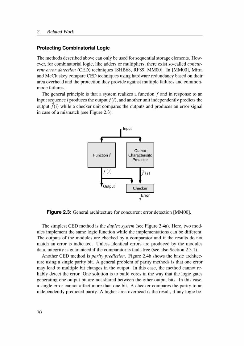
2. Related Work
Protecting Combinatorial Logic
The methods described above can only be used for sequential storage elements. How-ever, for combinatorial logic, like adders or multipliers, there exist so-called concur-rent error detection (CED) techniques [SHB68, RF89, MM00]. In [MM00], Mitraand McCluskey compare CED techniques using hardware redundancy based on theirarea overhead and the protection they provide against multiple failures and common-mode failures.
The general principle is that a system realizes a function f and in response to aninput sequence i produces the output f (i), and another unit independently predicts theoutput f (i) while a checker unit compares the outputs and produces an error signalin case of a mismatch (see Figure 2.3).
Function fOutput
CharacterisitcPredictor
Input
CheckerOutput
Error
f if i
Figure 2.3: General architecture for concurrent error detection [MM00].
The simplest CED method is the duplex system (see Figure 2.4a). Here, two mod-ules implement the same logic function while the implementations can be different.The outputs of the modules are checked by a comparator and if the results do notmatch an error is indicated. Unless identical errors are produced by the modulesdata, integrity is guaranteed if the comparator is fault-free (see also Section 2.3.1).
Another CED method is parity prediction. Figure 2.4b shows the basic architec-ture using a single parity bit. A general problem of parity methods is that one errormay lead to multiple bit changes in the output. In this case, the method cannot re-liably detect the error. One solution is to build cores in the way that the logic gatesgenerating one output bit are not shared between the other output bits. In this case,a single error cannot affect more than one bit. A checker compares the parity to anindependently predicted parity. A higher area overhead is the result, if any logic be-
70

2.3 Reliability: Measures against Faults and Errors
tween the different output bits is not shared. Parity prediction methods are shown,for example, in [Nic93], [TM97] and [NDMF97].
Module 1 Module 2
Comparator
Output Error
Input
Input
O1
O2
On
Predicted Parity P
Parity Checker
Output O1-O
nError
a) b)
Figure 2.4: On the left side, the duplex system is shown. On the right side, a CEDmethod using single parity bit prediction is shown. No logic sharingbetween the output bits is allowed [MM00].
Finally, there also exist methods which use unidirectional error codes. Thesemethods assume that all errors are unidirectional which means that either ’0’s changeto ’1’s or ’1’s change to ’0’s but not both. Berger codes and Bose-Lin codes are twounidirectional error detecting codes used for CED.
A Berger code-word is created by appending a binary string which includes thenumber of ’0’s (or the bit-wise complement of the number of ’1’s) in the given in-formation word (see Figure 2.5a). It requires some extra space and detects all uni-directional errors. Usually, these codes are used on communication channels; thebit-wise complement of ’1’s in the information word is represented by the check bits.It is important to notice that a single error causes unidirectional errors at the outputsand therefore logic circuits are restricted to be synthesized to be inverter-free (exceptat the primary inputs). Lo and others introduced a Berger code protected ALU in[LTRN92]. Pflanz and Vierhaus extend this approach by further protecting registersand shifters [PV01].
Using Bose-Lin codes (see Figure 2.5b), it is possible to detect t-bit unidirectionalerrors in the code word. The circuit also has to be inverter-free. Additionally, there isa restriction on the amount of logic sharing since the code can only detect t unidirec-tional errors [MM00].
Mitra and McCluskey analyze the overhead and the protection against temporaland permanent faults by simulation [MM00]. The area overhead of techniques forunidirectional error detecting codes (Berger, Bose-Lin) is quite high. Using parity
71

2. Related Work
a) b)
Logic Function(inverter-free)
Predict '1's count(inverter-
free)
Input
CheckerOutput
Error
Logic Function(inverter-free)
Predict 1s count(inverter-
free)
CheckerOutput
Error
Logic Function(inverter-free)
Max. Fanout2 outputs
Predict '1's count mod 4
(inverter-free)Max. Fanout
2 outputs
CheckerOutput
Error
Input
Figure 2.5: On the left side, a circuit which is protected by Berger codes is depicted.On the right side, a Bose-Lin code protected circuit with t = 2 is shown.For both methods, it is important that the combinatorial logic of thefunction and the code prediction circuit is inverter-free except of theprimary inputs [MM00].
prediction, the area overhead is smaller than using duplication. Note that routingoverhead has not been considered. Simulation showed that diverse duplication is thebest way to detect temporal and permanent faults, better than identical duplicationand parity prediction.
Joshi and others present a time redundancy based CED technique targeting invo-lutionary functions in [JWSK06]. A function is involutional if f ( f (x)) = x,∀x ∈ F .The proposed technique detects permanent and transient faults that affect the output.It can also detect permanent faults in a function even if the faults do not affect theoutput. This also enhances the security of the implementation since it is possible todetect attacks to the algorithm. The time overhead (after optimization) is less than8%, the area-overhead is less than 18% and the fault coverage is almost 100%. Thistechnique is primarily used in the domain of cryptography where a lot of involution-ary functions appear.
Almukhaizim and others proposes a concurrent error detection technique for com-binational and sequential logic [ADM04]. A state prediction of the next state of acontrol unit is calculated based on the current state and the inputs. The hardwareoverhead is typically smaller than in case of full redundancy on large state spaces.However, the method can only monitor the correct state transitions, but not the cor-rect storage of the state.
72

2.3 Reliability: Measures against Faults and Errors
2.3.4 Prevention and Detection of Single Event Effects
The prevention of single event effects can be done on the process level by applyingtriple wells or buried layers [MW04]. The goal is to drift the generated charges, pro-duced by an ionized particle impact, away from the active region. By using buriedjunctions in a triple well architecture, an opposite electrical field with respect to theNMOS-depletion is created which causes the drift of the electron-hole pairs, gener-ated by the particle impact, deep into the substrate. Furthermore, by replacing theradiating BPSG dielectric by purer mold components, the effect by thermal neutronscan be significantly lowered. The usage of silicon-on-insulator (SOI) can furtherincrease the robustness against soft errors by reducing the charge depth.
At the device level, the critical charge Qcrit stored inside a register cell can beincreased by increasing the capacitance or the voltage [MW04]. The capacitancecan be increased by using larger transistors. Both, however, raise the area and thepower overhead which restricts the applicability to selected nodes on critical partsof the circuit only. Memory cells which are insensitive to single event effects areintroduced in [CNV96] and [HKW+03]. These cells use more transistors which alsoincrease the area and power overhead. Mitra and others propose registers with built-in soft error resilience (BISER) for general logic in [MZS+08]. These registers arealso insensitive to single event effects.
To detect single event transients, Nicolaidis introduces a shadow register conceptin [Nic99]. A signal produced by combinatorial logic is sampled by multiple redun-dant registers with different clocks. The time lag δ between the rising edges of theclocks is greater than a typical single event effect. By using the original register andone shadow register, single event effects can be detected by comparing the registeredvalues. By using three registers, one original and two shadows with three differ-ent clocks, the single event effect can be corrected by a majority voter. A similarapproach is proposed by Mavis and Eaton [ME02].
Ernst and others use this technique with a main (original) and a shadow register todetect timing errors for dynamic voltage scaling (DVS) [EKD+03]. If timing errorsoccur, only the main register is affected due to the later sample point of the shadowregister. Therefore, if a timing error is detected, the value of the shadow register canbe fed back to the registers’ input. The penalty is a double latency for the operation.These enhanced registers are called Razor flip-flops. The approach is extended toadditionally detect and correct single event effects and variation-induced delay errorsby Das and others which is now called Razor-II [DTP+09].
A similar result is presented by [BZS+06], where Nicolaidis flip-flops are extendedwith an additional history register which can be used for rollbacks to correct errors.This technique is later combined with our control flow checking methods (see Section4 and in particular Section 4.5.5). The technique is extended with an ECC protectionfor detecting and correcting multiple errors [BZSH09]. Mehrara and others presentan approach to detect single event effects by doubled sampled latches [MAS+07].
73
2. Related Work
The correction is done by rollbacks to fixed checkpoints which separate the programinto so called epochs.
Some volatile FPGAs have an internal protection of the configuration memoryagainst single event upsets. A CRC value of the configuration memory is calculatedperiodically and compared to the CRC value stored in the configuration bitfile whichis calculated at bitfile generation [Alta].
2.4 Reliability and Security: Control FlowChecking
Control flow checking (CFC) denotes the task of checking the control flow of a pro-gram according to a given specification. The specification is derived mostly stati-cally at compile-time from the program. Control flow checking combines reliabilityand security issues and is a countermeasure against single event effect, degenerationfaults, code injection and invasive physical attacks.
Related work on control flow checking can be divided into completely software-based approaches and approaches using an additional hardware checker unit or awatchdog processor. Usually in these approaches, the program code is first structuredinto basic blocks3. Other approaches achieve control flow checking by redundantlydecoding the control flow instructions in an additional checker unit (e.g., [RLC+07]).
2.4.1 Software-Based Methods
Software-based control flow checking techniques belong to the so-called softwareimplemented hardware fault tolerance (SIHFT) methods. A famous software-basedCFC technique is called Control Flow Checking using Assertions (CCA) [KNKA96,MN98]. After the creation of the control flow graph (CFG, see also Section 4.3.2),special control instructions are inserted into the program code at the beginning and theend of a basic block (see Figure 2.6). The approach introduces two identifiers whichare set and checked with these instructions. At the entrance of a basic block, a basicblock identifier is assigned to a variable. Moreover, corresponding to the control flowgraph, a special control flow identifier is checked and subsequently set for the nextbasic block. At the end of a basic block, both identifiers are verified, so erroneousjumps or branches from or in the middle of a basic block are detected. By checkingthe control flow identifier, the correct processing order of the basic blocks is ensured.The advantage is that no hardware modules are required, however this approach has
3A basic block is a sequence of code which is executed successively without any jumps or branchesexcept, possibly, at the end. The basic block can only be left at the end of a block and can onlybe entered at the beginning. Only the last instruction can be a jump or branch and only the firstinstruction can be a jump or branch destination (see Section 4.3.2).
74
2.4 Reliability and Security: Control Flow Checking
impact on the performance of the program code and the erroneous jumps can only bechecked at the transitions of the basic blocks.
CPUProgram
Control Instructions
Control Instructions
BB1
BB2
BB3
Figure 2.6: Control instructions are usually inserted before and after a basic block(BB1-BB3) in software-based control flow checking approaches. Theadditional control flow instructions check the executed control flow ac-cording to the control flow graph.
The approach is enhanced for real-time distributed systems to achieve a lower per-formance overhead and faster error detection in [ANKA99]. The additional instruc-tions are inserted at an intermediate level of the compiler which makes this technique,called Enhanced Control Flow Checking with Assertions (ECCA), language indepen-dent.
Another software-based control flow checking approach called Block SignatureSelf Checking (BSSC) is introduced by Miremadi and others [MKGT92]. The codeis also structured into basic blocks and additional instructions are added at the entryand at the end of each block. Checking is done by storing a signature, e.g., the currentaddress, into a variable at the basic block entrance. Before leaving the basic block,this signature is verified. The method can verify the subsequent linear execution ofthe basic block. However, the processing of the correct basic block order cannot beverified.
Oh and others introduce a technique called Control Flow Checking by SoftwareSignatures (CFCSS) [OSM02]. A unique signature is assigned to each basic blockand the signature is embedded with the signature difference to the predecessor blockin the code. During the execution, a runtime signature is calculated and stored ina general purpose register. The signature of the last block and the stored signaturedifference are used to calculate and verify the current runtime signature at each basicblock entrance. In other words, this approach checks if the correct predecessor ofthe current basic block, according to the CFG, was processed. However, if a basic
75

2. Related Work
block has more than two predecessors, the method is not applicable. In this case, anadditional runtime variable is introduced to resolve the problem. Borin and otherspropose error classification for control flow checking and analyze the error coverageof the most existing software-based approaches [BWWA06]. Furthermore, they in-troduce two methods which are enhancements to the original CFCSS method. Thefirst method is called Edge Control Flow Checking (EdgCF) and the second is calledRegion Based Control Flow (RCF) technique.
Other similar approaches are SWIFT [RCV+05] and YACCA [GRRV03, GRRV05].All these method insert control instructions at the basic block borders into the pro-gram code, as depicted in Figure 2.6.
Bagchi and others introduce the Preemptive Control Signature (PECOS) checking,which is able to prevent jumps or branches in case of an error [BLW+01, BKIL03].The program code is equipped with additional checker instructions before each con-trol flow instruction. The runtime target address is determined and verified with thevalid target addresses, extracted from the compiled code. The list of valid target ad-dresses is stored inside the code, whereas the runtime target address is determined byloading the control flow instruction into a register and decode it by software. If theruntime target address is not in the list with valid addresses, an exception is triggeredwhich prevents the execution of the erroneous jump or branch. The drawback of thisapproach is that only the integrity of the control flow instruction in the memory ischecked. Transient faults, such as single event effects in the control path cannot bedetected by this method.
Abadi and others introduce a software-based CFC technique for security issuescalled Control Flow Integrity (CFI) [ABEL05, ABEL09]. This method focuses onindirect calls and returns. The destination of indirect calls and returns are determinedat compile-time, and each of these jump destination are labeled with a unique iden-tifier in the code. Instructions to check the identifier of the destination are added tothe program code before an indirect jump. Only if the identifier is correct, the jumpis executed. Budiu and others present an instruction set architecture (ISA) extensionwhich introduces new instructions for CFI hardware support [BEA06].
2.4.2 Methods using Watchdog ProcessorsA watchdog processor is a simple coprocessor which is able to monitor the behaviorof a main processor in order to detect errors [Lu82, MM88]. The predecessor of thewatchdog processor is the watchdog timer [CPW74, OCK+75]. A watchdog timeris reset by the program running on the main processor at certain intervals. If themonitored program hangs, the timer is not reset anymore. Therefore, the timer pro-duces an overflow which generates an interrupt. Inside the interrupt service routine,countermeasures can be started, e.g., the erroneous program can be terminated.
A watchdog processor is initialized with information about the main processor orthe process which should be monitored. At runtime, the watchdog processor concur-
76
2.4 Reliability and Security: Control Flow Checking
rently collects information about the execution of the program in the main processorand compares the gathered with initial information to detect errors. The informationmay include the memory access behavior, the control flow, the control signals, or thereasonability of results. Mahmood and McCluskey give a survey over error detec-tion with watchdog processors in [MM88]. Traditionally, a watchdog processor iscoupled with the main processor via a system bus. However, other approaches existwhere the watchdog processor is directly attached by dedicated signals.
The advantages of watchdog processors are the lower overhead than the duplicationof the main processor, the possibility of concurrently checking the execution whichresults in none or only little performance degeneration and the detection of commonor related design errors of the program or the processor due to the diversity of theprocessors architectures.
Watchdog processors, when used for control flow checking, have a watchdog pro-gram which is derived from the control flow of the checked program. The controlflow of a program can be represented in a graph whose nodes represent sequencesof code, e.g., basic blocks or whole functions, and the edges between the nodes rep-resent the control flow. An identifier, often called signature which is known by thewatchdog program is attached to each node. The signatures can be assigned at ran-dom or they can be derived form the instructions inside a node. Techniques usingthe arbitrarily assigned signatures are called assigned-signature control flow check-ing and techniques using the derived signature are called derived-signature controlflow checking [MM88]. The different watchdog processor approaches can be furthercategorized by the storage of the watchdog signatures. Therefore, the methods canbe divided into two groups, called Embedded Signature Monitoring (ESM) and Au-tonomous Signature Monitoring (ASM). ESM methods embed the watchdog signa-tures into the code of the checked program. To verify a signature, the correspondingsignature must first be transferred to the watchdog or to the main processor, depend-ing on the comparison location. The watchdog processors for the ASM methods havetheir own memory to store the signatures. Therefore, the watchdog must be initial-ized with all watchdog signatures before the program execution. In summary, thereexist four categories for control flow checking with watchdog processors (see Table2.1).
Watchdog-processor-based CFC approaches can be further categorized accordingto their error detection capability. The first category checks that the nodes are pro-cessed in an allowed sequence whereas approaches of the second category verify theinstruction sequence inside a node. The third category includes schemes which doboth [MM88].
Assigned-Signature Control Flow Checking
During the execution, the arbitrarily assigned signatures used for assigned-signatureCFC are transferred to the watchdog processor for verification. Usually, the trans-
77
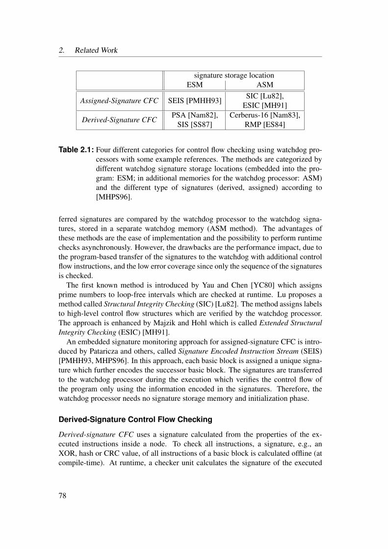
2. Related Work
signature storage locationESM ASM
Assigned-Signature CFC SEIS [PMHH93]SIC [Lu82],
ESIC [MH91]
Derived-Signature CFCPSA [Nam82], Cerberus-16 [Nam83],
SIS [SS87] RMP [ES84]
Table 2.1: Four different categories for control flow checking using watchdog pro-cessors with some example references. The methods are categorized bydifferent watchdog signature storage locations (embedded into the pro-gram: ESM; in additional memories for the watchdog processor: ASM)and the different type of signatures (derived, assigned) according to[MHPS96].
ferred signatures are compared by the watchdog processor to the watchdog signa-tures, stored in a separate watchdog memory (ASM method). The advantages ofthese methods are the ease of implementation and the possibility to perform runtimechecks asynchronously. However, the drawbacks are the performance impact, due tothe program-based transfer of the signatures to the watchdog with additional controlflow instructions, and the low error coverage since only the sequence of the signaturesis checked.
The first known method is introduced by Yau and Chen [YC80] which assignsprime numbers to loop-free intervals which are checked at runtime. Lu proposes amethod called Structural Integrity Checking (SIC) [Lu82]. The method assigns labelsto high-level control flow structures which are verified by the watchdog processor.The approach is enhanced by Majzik and Hohl which is called Extended StructuralIntegrity Checking (ESIC) [MH91].
An embedded signature monitoring approach for assigned-signature CFC is intro-duced by Pataricza and others, called Signature Encoded Instruction Stream (SEIS)[PMHH93, MHPS96]. In this approach, each basic block is assigned a unique signa-ture which further encodes the successor basic block. The signatures are transferredto the watchdog processor during the execution which verifies the control flow ofthe program only using the information encoded in the signatures. Therefore, thewatchdog processor needs no signature storage memory and initialization phase.
Derived-Signature Control Flow Checking
Derived-signature CFC uses a signature calculated from the properties of the ex-ecuted instructions inside a node. To check all instructions, a signature, e.g., anXOR, hash or CRC value, of all instructions of a basic block is calculated offline (atcompile-time). At runtime, a checker unit calculates the signature of the executed
78

2.4 Reliability and Security: Control Flow Checking
instruction in a basic block. When leaving a basic block, both signatures can becompared and errors inside the basic block can be detected. The derived-signatureCFC methods can also be categorized by the storage of the precalculated (golden)signature in ESM and ASM methods.
Embedded Signature Monitoring Derived-signature ESM methods store theoffline calculated signature (golden signature) in the program code with additionallyinserted instructions at the end or the beginning of each basic block. During run-time, the calculated signatures from the watchdog processor are compared to theseembedded signatures. The advantage of these methods is that all instructions can bechecked and a new program already contains the corresponding signature (see Fig-ure 2.7). The disadvantages are the performance impact and that a fault can onlybe detected at the end of a basic block which may be too late. Also, a single eventupset during the execution of the additionally inserted instructions can lead to a falsedetection or spoofing of an error.
CPU
Program
Control Instructions
Control Instructions
BB1
BB2
BB3
WatchdogProcessor
Figure 2.7: In the derived-signature ESM CFC approaches, a signature is calculatedfrom the executed instructions by a watchdog processor. The goldensignatures are calculated at compile-time and embedded with controlinstructions in the code. The additional control instructions read out theruntime calculated signature from the watchdog processor and compareit to the golden signature.
According to [MM88], the first derived-signature CFC method is introduced byNamjoo [Nam82] and is called Basic Path Signature Analysis (Basic PSA). The sig-natures are calculated by XORing over all instructions inside each basic block. Afterthe calculation of the signatures at compile-time, the signatures are stored at the be-ginning of each basic block. The watchdog processor monitors the instruction streamand identifies the loading of the signature from the instruction memory. During the
79
2. Related Work
execution of the basic block, the watchdog processor calculates the runtime signatureby XORing the processed instructions and, at the end of a basic block, the signaturesare compared. A very similar technique is proposed by Sidhar and Thatte in [ST82].
Other approaches use linear feedback shift registers (LFSR) [DS90, DS91] orchecksums [SM90] as signatures or try to lower the number of used signatures by us-ing larger blocks which include multiple branches [SS87, WS90]. Gaisler enhancedhis ERC32 processor with an ESM CFC technique where the signatures are embed-ded into NOP instructions [Gai94]. Meixner and others store the signatures for theArgus-1 checker into unused instruction bits of the SPARC ISA to reduce the perfor-mance and memory overhead of their ESM method [MBS07, MBS08]. If insufficientunused bits are available, they also embed the signature into NOP instructions.
Upadhyaya and Ramamurth propose a derived-signature CFC technique using m-of-n codes [UR94]. An m-of-n code is an n-bit code whose bit values have m ones. Atcompile-time, the signature of a basic block is calculated, for example, by XORingthe instructions. If the intermediate result is an m-of-n code, then this instructionis tagged. At runtime, the watchdog calculates the signature, recognizes the taggedinstructions and verifies on the tagged instructions if the runtime signature is an m-of-n code. At the basic block borders, an additional byte is inserted which adjuststhe current signature to an m-of-n code in order to force a check. The advantage isthat the signature must not be stored in the program code. However, one additionalbyte per branch is necessary to force a check in order to restart the runtime signaturecalculation at a new basic block. A similar approach is presented by Ohlsson andRimen called Implicit Signature Checking (ISC) [OR95]. The implicit signaturesare the current start addresses of the basic blocks. This can be achieved by usingadditional justified signatures embedded into the code.
Autonomous Signature Monitoring The golden (compile-time calculated) sig-natures of derived-signature ASM methods are stored in a separate memory for thewatchdog processor. The comparison between the golden and the runtime calculatedsignature is implemented in hardware (see Figure 2.8). If the control flow graphis mapped into the instruction memory of the watchdog processor, the jumps andbranch destinations can also be checked. The advantages are that the program codedoes not need to be altered and that there is no performance impact. Also, all in-structions can be monitored. The disadvantages are that extra memory is requiredfor the checker unit and the synchronization between the CPU and the checker unit isdifficult. Therefore, interrupts, multi threading, and indirect jumps cannot be coveredcompletely.
One of the first approaches using the ASM scheme is the Cerberus-16 watchdogprocessor [MM88, Nam83]. The control flow graph and the corresponding signa-tures are mapped in the microinstructions which are stored into the watchdog pro-cessor memory. The Cerberus-16 processor only has control flow instructions with
80

2.4 Reliability and Security: Control Flow Checking
CPU
Program
BB1
BB2
BB3
WatchdogProcessor
Control Instructions
BB1BB2BB3
Figure 2.8: In the derived-signature ASM approach, the watchdog processor hasa separate memory for storing the control instructions. The executionmust be synchronized between the CPU and the watchdog processor.
encoded signatures and instructions for the communication with the main processor.The processing of the control flow of the main and the watchdog processor are com-pletely synchronized. The approach is extended by Michel and others by a branchaddress hashing (BAH) technique, now called Watchdog Direct Processing (WDP)which reduces the memory overhead for the watchdog processor memory [MLS91].
An asynchronous ASM approach is presented by Eifert and Shen [ES84, ST87]which is called Roving Monitor Processor (RMP). At compile-time, the control flowof the program is extracted and the signatures (CRC values) are calculated. Duringthe execution, the runtime signatures are calculated with an additional signature gen-eration unit and, at the end of a block, the calculated signature is sent to the watchdogprocessor. The watchdog compares the received signature to the signatures achievedfrom the control flow graph and stores then in the watchdog memory. At branches,the received signature is compared with the two successor signatures of the currentnode in order to determine the next signature. This approach can also be used tocheck multi-processor systems where each processor has its own signature genera-tion unit and sends the signature via a signature queue to the watchdog processorwhich is responsible for the whole system. The approach is extended by Madeira andSilva who introduce the Online Signature Learning and Checking (OSLC) technique.In this approach, the golden signature is generated during a learning phase [MS91].The learned signatures are stored in the watchdog memory of an RMP-like watchdogprocessor.
Arora and others describe an ASM approach for security applications in [ARRJ06].This hardware approach consists of three parts: the Inter-Procedural CFC, the Intra-Procedural CFC, and the Instruction Stream Integrity Checker. The Inter-ProceduralCFC verifies the function calls and returns by implementing the function call graph
81

2. Related Work
in hardware using content addressable memories (CAMs) and an FSM. The Intra-Procedural CFC checks the basic blocks by a compile-time generated control flowgraph, implemented in checker memories. Finally, the Instruction Stream IntegrityChecker is similar to those of other ASM methods, however, they use hash functionsto generate and verify the signatures.
Our new control flow checking approach introduced in Section 4 belongs to theclass of derived-signature ASM methods. We propose a term checker unit for thewatchdog processor, because our unit is very simple with only few hardware over-head. However, like in the Cerberus-16 or the WDP approach, the control flow graphis mapped into microinstructions which are stored in a separate memory. Furtheradvantages of our control flow checker are the fast error detection due to the tight in-tegration into the processor, the error recovery possibility, and the expandability withmodules which support more control flow instructions or detect more errors. More-over, like the other ASM-methods we have no performance impact on the error-freecase and the program must not be altered.
2.5 SummaryThis chapter gives an overview of methods and techniques to increase the securityand reliability of embedded systems. The focus of this survey is on IP protection andcontrol flow checking which correlates with the following chapters. In addition to theintroduced methods, there exist security and reliability frameworks which combinemany of these techniques, for example, the RSE framework [NKIX04] or the Arguschecker [MBS08]. Nevertheless, this survey is far away from being complete, ratherits purpose is to give an impression of the different research areas of this topic. Therelevance increases more and more with the ongoing growing of complexity due tothe advances in technology.
82
3IP Core Watermarking and
Identification
In this chapter, methods for IP core watermarking and identification as well as theirimplementations are presented. First, we give an introduction to the topic and statethe goals of the proposed methods. The following section presents a theoretical modelfor watermarking and identification of IP cores. We proceed by introducing methodsfor extracting a watermark and verifying the authorship by IP core identification us-ing an FPGA bitfile. The subsequent section explains the extraction of a watermarkby analyzing the power consumption of the FPGA. After that, we provide experi-mental results for all introduced methods. In conclusion, the contributions will besummarized.
3.1 Introduction
The ongoing miniaturization of on-chip structures allows us to implement very com-plex designs which require very careful engineering and an enormous effort for de-bugging and verification. Indeed, complexity has risen to such enormous measuresthat it is no longer possible to keep up with productivity demands if all parts of adesign must be developed from scratch. In addition, the very lively market for em-bedded systems with its demand for very short product cycles intensifies this problemsignificantly. A popular solution to close this so called productivity gap is to reusedesign components that are available in-house or that have been acquired from othercompanies. The constantly growing demand for ready to use design components,
83
3. IP Core Watermarking and Identification
also known as IP cores, has created a very lucrative and flourishing market which isvery likely to continue its current path not only into the near future.
One problem of IP cores is the lack of protection mechanisms against unlicensedusage. A possible solution is to hide a unique signature (watermark) inside the core.However, there also exist techniques where an IP core can be identified without anadditional signature. Identification methods are based on the extraction of uniquecharacteristics of the IP core, e.g., lookup table contents for FPGA IP cores. Withthese techniques, the author of the core can be identified and an unlicensed usage canbe proven. In this chapter, watermarking as well as identification techniques for IPcores will be presented.
Our vision is that unlicensed IP cores, embedded in a complete SoC design whichcould be further embedded into a product, can be detected solely by using the givenproduct and information from the IP core developer. Information of the accused SoCdeveloper or product manufacturer should not be necessary and no extra informationshould be required from the accused company. Obviously, such concepts need ad-vanced verification techniques to detect a signature or certain IP core characteristics,present in one of many IP cores inside a system. Furthermore, the embedded authoridentification should be preserved even when the IP cores pass through different de-sign flow steps. On the one hand, we must deal with the problem that design toolsmight remove the signature or the characteristics during synthesis and optimization.On the other hand, we must also secure the signature or characteristics against the re-moval by pirates which do not want the IP core be identifiable. Licensing IP cores isa market where a lot of money is involved and if a company decides to use unlicensedcores, e.g., to lower the production costs, they usually have very high skilled employ-ees who might try to remove or bypass the watermark or identifying techniques.
In Figure 3.1, a possible watermarking flow is depicted. An IP core developer em-beds a signature inside his core using a watermark embedder and sells the protectedIP core. A third-party company may obtain an unlicensed copy of the protected IPcore and use it in one of their products. If the IP core developer becomes suspiciousthat his core might have been used in a certain product without proper licensing, hecan simply acquire the product and check for the presence of his signature. If thisattempt is successful and his signature presents a strong enough proof of authorship,the original core developer may decide to accuse the product manufacturer of IP fraudand press legal charges.
An extensive survey regarding existing watermark techniques was already givenin Section 2.1. The major drawback of these approaches is the limitation of theverification possibilities of the watermarked core. Our verification strategy solelyrequires the fishy product and no additional information from the producer.
IP cores exist for all design flow levels, from HDL cores at RTL to bitfile coresfor FPGAs or layout cores for ASIC designs at device level (see Section 1.2.7). Inthe future, IP core companies will concentrate more and more on the flexible HDL
84

3.1 Introduction
Signature
IP Core developer
=
IP Core
A Watermark Embedder
WatermarkedIP Core A
Product developer
WatermarkedIP Core
ProductImplementation
WatermarkedIP Core A
IP Core
ProductProduct
Watermark Extractor
Signature
ASignature
B
?
Buy Product
e.g., Copy Attack
B
Sell IP Cores
Obtain unlicensed Core
Figure 3.1: This figure shows a typical watermarking flow: An IP core developerembeds a watermark A inside his core. If a product developer obtainsan unlicensed core and embeds this core in his product, the IP coredeveloper can buy this product and extract the watermarks of all usedIP cores. Now, he is able to compare his signature with the extractedsignatures.
and netlist cores. One reason for this development is that these cores can be easilyadapted to new technologies and different FPGA devices.
This chapter focuses on watermarking and identification methods for IP cores im-plemented on FPGAs. These have a huge market segment and the inhibition thresholdfor using unlicensed cores is lower than in the ASIC market where products are pro-duced in high volumes and millions for mask production are spent. Nevertheless,some of these methods can be adapted for the ASIC design flow as well. Moreover,we concentrate on flexible IP cores which are delivered at RTL or logic level in HDLor netlist format. The advantage is that these cores can be used in different FPGAdevices and can be combined with other cores to provide a complete SoC solution.Most of the existing watermarking techniques do not cover the area of HDL or netlistcores, or are not able to easily extract the signature from a heterogeneous SoC imple-mentation in a given product.
The problem of applying watermarking techniques to FPGA designs is not thecoding and insertion of a watermark, rather the verification with an FPGA embed-
85

3. IP Core Watermarking and Identification
ded in a system. Hence, our methods concentrate particularly on the verification ofwatermarks. In general, there are five potential sources of information:
• Bitfile,
• Ports,
• Power,
• Electromagnetic (EM) radiation, and
• Temperature.
The bitfile of an FPGA can be extracted by wire tapping the communication be-tween the PROM and the FPGA. But some FPGA manufactures provide an optionto encrypt the bitstream. The bitfile is stored in the PROM in encrypted form andwill be decrypted inside the FPGA. Monitoring the communication between PROMand FPGA in this case is useless, because only the encrypted file will be transmitted.The bitfile is a proprietary format which is not documented by the FPGA manufac-turers. However, it seems to be possible to read out some parts of the bitfile such asinformation stored in RAMs or lookup tables. This makes it possible to evaluate thelookup tables of a design. In Section 3.3, we introduce bitfile watermarking methods.Note that we use the term “bitfile watermarking” for extracting the watermark of thebitfile. The insertion of the watermark and the delivery of the core to the customercan also be done at the RTL or logic level. If we mean the insertion of a watermarkat bitfile level, we use the term “watermarking for bitfile cores”.
Another popular approach for retrieving a signature from an FPGA is to employunused ports. Although this method works for top-level designs, it is impractical forIP cores, since these are mostly components that will be embedded into a design sothat the ports will not be accessible any more. Due to these restrictions, we do notdiscuss the extraction of watermarks over output ports.
In this thesis, we present a new and unique technique to read out the signature byanalyzing the power of an FPGA. We show that the clock frequency and togglinglogic can be extracted from the power spectrum. The basic idea behind these tech-niques is thus to force a certain toggle pattern and extract this signature from theFPGA’s power spectrum. We present the basics of these new methods with many ex-tensions in Section 3.4. We use the term “Power Watermarking” to refer to collectingthe signature from the FPGA’s power consumption.
Detecting a signature using the electromagnetic (EM) spectrum uses almost thesame strategy. This technique has the further advantage that a raster scan of an FPGAsurface with an EM sensor can also use the location information to extract and ver-ify the watermark. Unfortunately, more and more FPGAs are delivered in a metalchip package which absorbs the EM radiation. Nevertheless, this is an interestingalternative technique for extracting watermarks and invites for future research.
86

3.2 Theoretical Watermark Model
Finally, a watermark might also be read out by monitoring the temperature ra-diation. The concept is similar to the power or EM-field watermarking approach,however, the transmission speed is drastically reduced. Interestingly, this is the onlywatermarking approach which is commercially available [KMM08]. Here, readingthe watermark embedded into an FPGA design may need up to 10 minutes.
3.2 Theoretical Watermark Model
In this section, we propose a theoretical watermarking model. With this model, dif-ferent threats and attack scenarios can be described and evaluated. In general, wa-termarking techniques must deal with an uncontrolled area, where the watermarkedwork is further processed. This is true for multimedia watermarking, where, e.g.,watermarked images are processed to enhance the image quality by filters or for IPcore watermarking where the core is combined with other cores and traverses otherdesign flow steps. However, the watermarked work may be exposed further to attacksin this uncontrolled area that may destroy or negate the watermark and thus the proofof authorship as well. This uncontrolled area is difficult to describe in a precise wayand therefore, the security goals and issues for watermarking are often described innatural language which results in an imprecise description. This natural descriptionmakes an assessment of the security very difficult, particularly if the attackers areintelligent and creative.
Introducing a defined theoretical watermarking model with attackers and threatsallows us to assess the security of general watermarking techniques. However, itshould be noted that the model has to cover all possible attack scenarios and representall aspects of the real world behavior to allow for a meaningful assessment of thesecurity. In this section, we present a general watermark model introduced by Li etal. [LMS06] which will be enhanced with aspects of IP core watermarking.
3.2.1 General Watermark Model
Watermarking intellectual property can be specified precisely by characterizing theinvolved actions using a security model. We use the standard definitions from secu-rity theory, which defines security goals, threats and attacks. Security goals representcertain abilities of a scheme, which are important to protect in order to keep its func-tionality in tact. These abilities may be violated by threats which are realized byattacks. Regarding watermarking, the overall security goal is to be able to presenta proof of authorship that is strong enough to hold in front of a court. The secu-rity goal of a watermark scheme is violated if the original author cannot produce astrong enough proof of authorship, so that a dispute with another party will lead to anownership deadlock, but also in the occasion, that another party is able to present amore convincing proof of authorship than the original author, resulting in counterfeit
87
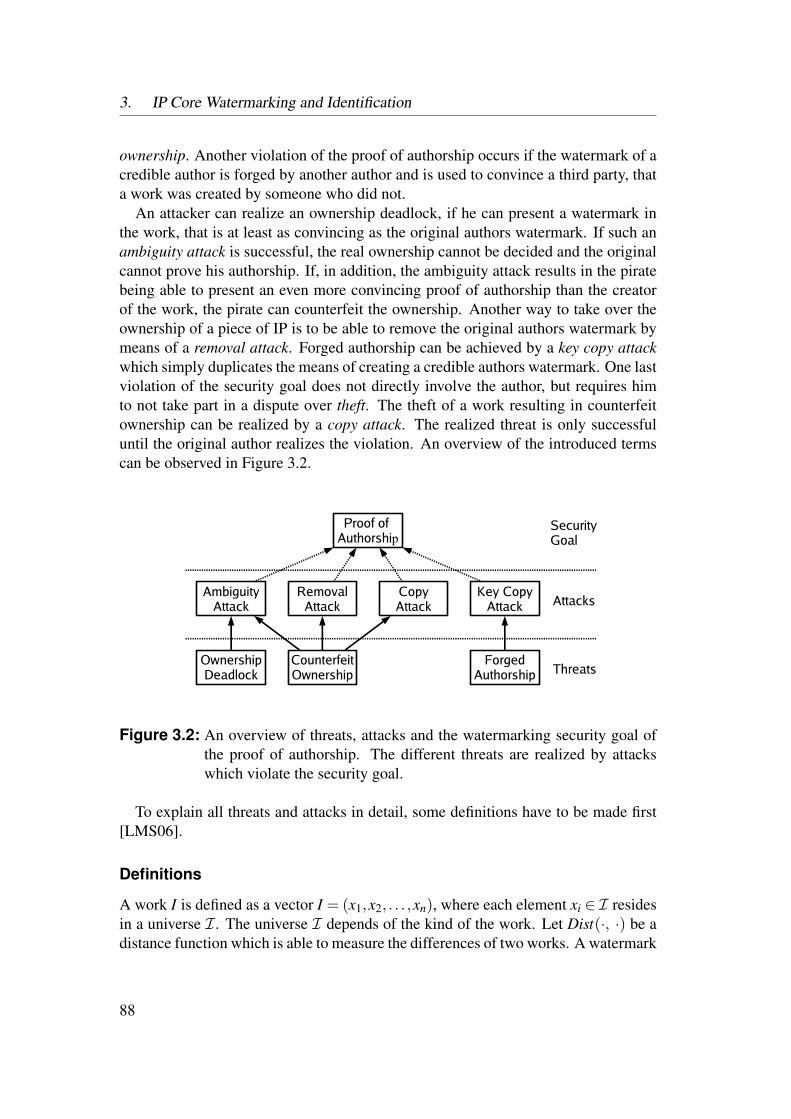
3. IP Core Watermarking and Identification
ownership. Another violation of the proof of authorship occurs if the watermark of acredible author is forged by another author and is used to convince a third party, thata work was created by someone who did not.
An attacker can realize an ownership deadlock, if he can present a watermark inthe work, that is at least as convincing as the original authors watermark. If such anambiguity attack is successful, the real ownership cannot be decided and the originalcannot prove his authorship. If, in addition, the ambiguity attack results in the piratebeing able to present an even more convincing proof of authorship than the creatorof the work, the pirate can counterfeit the ownership. Another way to take over theownership of a piece of IP is to be able to remove the original authors watermark bymeans of a removal attack. Forged authorship can be achieved by a key copy attackwhich simply duplicates the means of creating a credible authors watermark. One lastviolation of the security goal does not directly involve the author, but requires himto not take part in a dispute over theft. The theft of a work resulting in counterfeitownership can be realized by a copy attack. The realized threat is only successfuluntil the original author realizes the violation. An overview of the introduced termscan be observed in Figure 3.2.
Proof of Authorship
OwnershipDeadlock
CounterfeitOwnership
ForgedAuthorship
AmbiguityAttack
RemovalAttack
CopyAttack
Key CopyAttack
Security Goal
Threats
Attacks
Figure 3.2: An overview of threats, attacks and the watermarking security goal ofthe proof of authorship. The different threats are realized by attackswhich violate the security goal.
To explain all threats and attacks in detail, some definitions have to be made first[LMS06].
Definitions
A work I is defined as a vector I = (x1,x2, . . . ,xn), where each element xi ∈ I residesin a universe I. The universe I depends of the kind of the work. Let Dist(·, ·) be adistance function which is able to measure the differences of two works. A watermark
88
3.2 Theoretical Watermark Model
W is a vector W = (w1,w2, . . . ,wl), where each element wi ∈W . The universeW isdependent on the universe of the work I and the watermark generation process. Akey K is a sequence of m binary bits (K = 0, 1m).
In the general watermark model, there exist three algorithms: the watermark gen-erator G, the watermark embedder E , and the watermark detector D. The watermarkgenerator G is able to generate a watermark W in the universe W for the key K:W = G(K). The watermark embedder E embeds this watermark W into the work I.The output is the watermarked work I = E(I,W ). The watermark in I should obvi-ously not be visible. Therefore, the difference between I and I should be small. Withthe distance function, this can be expressed as Dist(I, I) < tI , where tI is a thresholdvalue upon the difference is noticeable. Using the watermark detector D, the exis-tence of the watermark W in the work I can be proven, if D(I,W ) = true or negatedif D(I,W ) = f alse.
This watermarking model may exist in different variations. The detection may beachieved with a watermarking extractor X instead of the watermark detector D. Thewatermark extractor X uses the watermarked work I as input and the extracted keyKX as output: KX =X (I). If no watermark is present in the work I, the watermark ex-tractor indicates this conveniently. Another extractor variant needs the watermarkedand the original work as input: KX = X (I, I). The extracted key KX can now becompared with the authors key K to establish the ownership.
Threat Model
The different threats against the security goal to establish the authorship of a work canbe explained using attack examples. Let an author create a work IA and a watermarkWA using his key KA with the watermark generator G: WA = G(KA). The author’swork is now watermarked with the watermark embedder E : IA = E(IA,WA). Thewatermarked work IA is published. The work can be modified by third parties, e.g.,by filtering a watermarked image, so several variants IAx of IA may exist. For allvariants, it is necessary that the difference to IA is smaller than a specified thresholdtI: Dist(IAx , IA) < tI,∀x. This condition is necessary, because if a work is completelyor exhaustively altered, the relation to IA is weak, and the work can be counted asa new work. Let I be a published work where the authorship is to be proven. Wepropose different scenarios where an attacker or pirate tries to sabotage the proof ofauthorship (see also Figure 3.2):
The first scenario is counterfeit ownership using a removal attack. The pirate ob-tains the watermarked work IA from the author or any variant of it (IAx) and managesto remove the watermark and transforms the obtained worked into a work without orwith a disabled watermark I. If the author of the work tries to proof his ownership ofthe work I, he fails:
Owner : Dist( IA , I ) < tI D(I,WA) = f alse
89

3. IP Core Watermarking and Identification
Furthermore, the pirate can embed his watermark WP into the work to take overthe ownership: IP = E(I,WP). For the proof, he presents the work with the removedwatermark I as original work.
Pirate : Dist( I , IP ) < tI D(IP,WP) = true
The next scenario is counterfeit ownership by using a copy attack where a workis copied without the permission from the author. To realize a counterfeit ownershipwith a simple copy attack, the original author must be passive, either if he publishes awork which is not watermarked, or publishes a watermarked work, but does not takenot part in the dispute. In both cases, the pirate can embed his watermark WP into thework I.
Pirate : IP = E(I,WP) Dist( I , IP ) < tI D(IP,WP) = true
If the author had not watermarked the work, he has no possibility to proof his au-thorship, whereas otherwise, by detecting his watermark in I and IP, he can establishthe authorship. Here, the author has shown that his watermark WA is present in thefake original work from the pirate I, whereas the pirate’s watermark WP is not in theoriginal work IA of the author. This proves that the pirate has taken a watermarkedwork from the author and embedded his watermark in it.
Owner : Dist( IA , IP ) < tI D(IP,WA) = true D(I,WA) = truePirate : Dist( I , IP ) < tI D(IP,WP) = true D(IA,WP) = f alse
In the next scenarios, the pirate analyzes the work I in order to find a fake wa-termark WP and a corresponding fake original work IP. This leads to an ownershipdeadlock by using an ambiguity attack. Both parties can show that the work I is wa-termarked with their corresponding watermarks and furthermore, the own watermarkis present in the original work of the opponent. This leads to an ownership deadlock,because the rightful owner cannot be chosen.
Owner : Dist( IA , I ) < tI D(I,WA) = true D(IP,WA) = truePirate : Dist( IP , I ) < tI D(I,WP) = true D(IA,WP) = true
Moreover, if the pirate can achieve that in his fake original work IP the watermarkof the author WA cannot be found, he can take over the ownership. This ambiguityattack leads to a counterfeit ownership.
Owner : Dist( IA , I ) < tI D(I,WA) = true D(IP,WA) = f alsePirate : Dist( IP , I ) < tI D(I,WP) = true D(IA,WP) = true
Forged authorship can be achieved by key copy attacks. Here, the key KA of acredible author is stolen, and a fake watermark W ′A is generated. With this watermark,
90

3.2 Theoretical Watermark Model
a work with lower quality IP is marked. The pirates goal is that everyone believesthat this poor work is from the credible author which might raise the value of his ownwork.
Pirate : W ′A = G(KA) IA′= E(IP,W ′A) D(IA
′,W ′A) = true
In the following, some security properties of a watermark scheme will be analyzedwith respect to the attacks and threats introduced above. Let attacker A be any algo-rithm of polynomial complexity.
Definition 3.1 A watermark scheme is tI-resistant to removal attacks if for any at-tackerA and given any work I watermarked by W, it is computationally infeasible forA to compute any work I′ such that Dist(I, I′) < tI and D(I′,W ) = f alse [LMS06].
The term tI-resistant means that the watermark scheme is resistant against removalattacks with respect to the threshold value tI . If the distance exceeds tI , the workscannot be counted as identical. For example, if the attacker creates a completelynew work, the watermark is also removed, but the works are not the same. Thephrase computationally infeasible follows the standard definition from cryptography.Something is computationally infeasible if the costs (e.g., memory, runtime, area) isfinite but impossibly large [DH76]. Here, this is true if the probability Pr[A(I) = I′]is negligible with respect to the problem size n. A quantity X is negligible withrespect to n if and only if for all sufficiently large n and any fixed polynomial q(·) (theattackerA is defined as an algorithm of polynomial complexity), we have X < 1/q(n)[LMS06].
In other words, with a sufficiently large problem size of watermarked work I, re-sistance against removal attacks means that the attacker is unable to remove the wa-termark as the problem size is beyond the computational capability of the attacker,unless the resulting work is perceptually different from the original work.
If we consider ambiguity attacks where a possible attacker finds a fake watermarkinside a watermarked work, we come to the following definition:
Definition 3.2 A watermark scheme is resistant to ambiguity attacks if for any at-tacker A and any work I, it is computationally infeasible for A to compute a validwatermark WP such that D(I,WP) = true [LMS06].
A watermark scheme cannot be resistant against copy attacks, because the water-mark scheme cannot distinguish if the work which is used as original work is reallythe work of the person which is identified by the key.
In case of key copy attacks, the key of a credible author is used to watermark awork with lower quality. In general, it should be impossible for an attacker to createa work I′ which is distinguishable from any work of another author where the key orwatermark of a credible author can be found.
91

3. IP Core Watermarking and Identification
Definition 3.3 A watermarking scheme is tI-resistant to key copy attacks if for anyattacker A and any work I = E(I,W ) for some original I and the watermark W, it iscomputationally infeasible for A to compute a work I′ such that Dist(I, I′) > tI , yetD(I′,W ) = true [LMS06].
To prevent key copy attacks, a private/public key algorithm, like RSA [RSA78] canbe used. RSA is an asymmetrical cryptography method. It is based on factorization ofa number into prime numbers. The author encrypts a message which clearly identifiesthe author and the work with his private key. The work can be identified by a hashvalue over the original work. This encrypted message is now used for generatingthe watermark and embedded inside the work. Stealing this watermark is useless,because everyone can decrypt the message with the public key, whereas no one canalter this message.
3.2.2 IP Core Watermark Model
Watermarking IP cores in electronic design automation is in some aspects differentfrom multimedia watermarking (image, audio, etc.). An essential difference is thatwatermarking should preserve the functionality of the core. Another difference isthat IP cores can be distributed at different abstraction levels which have completelydifferent properties for the watermark security against attacks. We define differentdesign steps as different technology or abstraction levels a work or IP core can bespecified on (see Section 1.2.7). On higher abstraction levels, e.g., the architecturelevel or RTL, the functionality is described by an algorithm which should be imple-mented. At these levels, mainly the behavior is described and the representation isoptimized for easy reading and understanding the algorithm. During the course of thedesign flow, more and more information is added. For example, at the device levelalso placement information is included in the representation of the core. Extractingonly the relevant information about the behavior of the algorithm is much harder thanat higher abstraction levels. Furthermore, the information at lower abstraction levelsis usually interpreted by tools rather than humans. The representation of this infor-mation is therefore optimized for tools and not for human readability. For example,consider an FPGA design flow. Here, three different abstraction levels exist: RTL,logic, and device level. An algorithm, specified at the register-transfer-level (RTL) inan HDL core is easier to understand than a synthesized algorithm at the logic level,represented by a netlist. In summary, we can say that the behavior of an algorithm iseasier to understand on higher abstraction levels than on the lower ones.
Transformations from a higher to a lower abstraction level are usually done by de-sign tools. For example, a synthesis tool is able to transform a HDL core specified atthe register-transfer-level (RTL) into its representation on the logic level. Transfor-mations from a lower to a higher level can be achieved by reverse engineering. Here,usually no common tools are available. One exception is the Java library JBits from
92
3.2 Theoretical Watermark Model
Xilinx [Xilc] which is able to interpret the bitfiles of Virtex-II device types. Thus,it is possible to transfer a bitfile core into a netlist at the logic level by using JBits.However, in general, reverse engineering must be considered as very challenging taskwhich may cause high costs.
A watermark can be embedded at every abstraction level. Furthermore, the water-marked core can be published and distributed also at every abstraction level whichmust not necessarily be the same level at which the watermark was embedded. How-ever, the extraction of the watermark is usually done in the lowest abstraction level,because this representation is implemented into the end product.
Hiding a watermark at a lower abstraction level is easier, because first, there aremore possibilities of how and where to hide the watermark. Second, the informationstored at these abstraction levels is usually outside the reception area of the humandeveloper.
Definitions
Our new definitions for the IP core watermarking model [SZT08] are derived fromthe general watermarking model introduced in the beginning of this section. A workor IP core that is specified at abstraction level Y is denoted by IY = (xY1,xY2, . . . ,xYm),where each xYi ∈IY is an element of the work, and IY is a universe, inherent to the ab-straction level Y . For example, an FPGA design at the device abstraction level mightbe represented by a bitfile which can be characterized as a work IB = (xB1, . . . ,xBm),whose elements reside in the universe Bit (IB). Hence, a bitfile IB with |IB| = m canalso be considered as a binary sequence IB = 0,1m.
Let T (·) be a transformation, which transforms a work on a specific abstractionlevel into a work of another abstraction level. A transformation from the higher levelY to the lower abstraction level Z is denoted TY→Z(·), whereas a transformation froma lower to a higher level is denoted TY←Z(·).
The distance function DistY (·, ·) in the context of IP core watermarking is onlyable to compare two works of the same abstraction level. If the distance of two IPcores IY and I′Y of the same abstraction level Y is smaller than a threshold value tI(DistY (IY , I′Y ) < tI), the two works may be considered similar.
Furthermore, the watermark generator G, embedder E , and detector D must berestricted in a way that they cannot cross the abstraction level boundaries. In detail,a specific watermark generator GX(·) is able to generate a watermark WX for theabstraction level X from a key K: WX =GX(K). The input of the watermark embedderor detector must be in the same abstraction level. For example, to watermark an IPcore IX at abstraction level X , also the watermark WX must be generated for thisabstraction level. So to obtain a watermarked work on the abstraction level X , it isnecessary to also use a watermarked and an embedding algorithm suitable for thesame abstraction level, i.e., IX = EX(IX ,WX).
93
3. IP Core Watermarking and Identification
In order to achieve full transparency of the watermarking process towards designtools, it is an essential requirement that a work, marked on any abstraction level,will retain the watermark if transformed to a lower abstraction level. Hence, ifDY (IY ,WY ) = true, so should also D(IZ,WZ) = true, if IZ = TY→Z(IY ), and WZ isa representation of WY on abstraction level Z.
However, considering reverse engineering, the watermark information is may beremoved by the reverse engineering transformation TY←Z(·), or the detection andremoval of the watermark may be easier on the higher abstraction level. For example,consider an FPGA bitfile IP core watermarking technique for which the watermark isstored in some placement information inside the bitfile. The watermark is generatedfor bitfiles at device level: WB = GB(K). The watermark is embedded in a bitfile coreIB to create the watermarked bitfile: IB = EB(IB,WB). If an attacker is able to reverseengineer the bitfile and reconstruct a netlist at logic level the placement informationwill get lost, since there is no representation for this on the logic level. This implies,of course, that the watermark is lost, as well: IL = TL←B(IB), DL(IL,WL) = f alse.Another problem of reverse engineering may be that an embedded watermark mightbecome obviously readable at the higher abstraction level and can be removed easily.
Figure 3.3 shows an example of the IP core watermark model considering differentabstraction levels.
Threat Model
The threat and attack model for general watermarking, as depicted in Figure 3.2, mayremain almost the same for the IP core watermarking model. However, the resistancedefinitions against different attacks must be redefined. Sometimes, it might be easierfor an attacker to redevelop an IP core than to remove a watermark. The questionto purchase or to redevelop a core is a pure matter of cost. An uprising economicalquestion is whether the development of an attack is an option. For many cases, theredevelopment from scratch might be cheaper than obtaining an unlicensed core anddevelop an attack in order to remove the watermark. On the other hand, there aredesigns involving such cunning cleverness and creativity that trying to redevelop awork of equivalent economic value would exceed the costs of developing an appro-priate attack by several orders of magnitude.
In the general watermarking model, it should be computationally infeasible to re-move the watermark without changing the properties of the work. For the introducedIP core watermarking model, this requirement does not necessarily hold. We mayconsider a watermarking technique secure, if the cost for obtaining an unlicensed IPcore and developing a removal attack is higher than to purchase the IP core.
Let the attacker AY be an algorithm which is able to transform a watermarked IPcore IY at the abstraction level Y into an IP core with removed or disabled water-mark I′Y = AY (IY ). Let C(·) be a cost function. Furthermore, let CD(·) denote thedevelopment cost of a specified IP core or attack and CP(·) the purchase cost of an
94
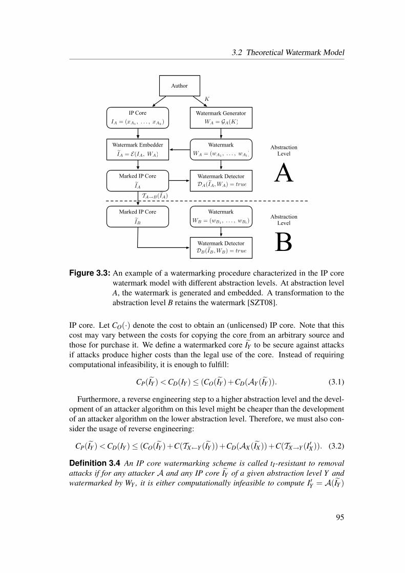
3.2 Theoretical Watermark Model
TA→B(IA)
AbstractionLevel
A
K
Author
IA = (xA1 , . . . , xAk)
IP CoreWA = GA(K)
Watermark Generator
WA = (wA1 , . . . , wAl)
WatermarkIA = E(IA, WA)
Watermark Embedder
IA
Marked IP Core Watermark Detector
IB
Marked IP CoreWB = (wB1 , . . . , wBl
)Watermark
Watermark Detector
AbstractionLevel
B
DA(IA, WA) = true
DB(IB , WB) = true
Figure 3.3: An example of a watermarking procedure characterized in the IP corewatermark model with different abstraction levels. At abstraction levelA, the watermark is generated and embedded. A transformation to theabstraction level B retains the watermark [SZT08].
IP core. Let CO(·) denote the cost to obtain an (unlicensed) IP core. Note that thiscost may vary between the costs for copying the core from an arbitrary source andthose for purchase it. We define a watermarked core IY to be secure against attacksif attacks produce higher costs than the legal use of the core. Instead of requiringcomputational infeasibility, it is enough to fulfill:
CP(IY ) < CD(IY )≤ (CO(IY )+CD(AY (IY )). (3.1)
Furthermore, a reverse engineering step to a higher abstraction level and the devel-opment of an attacker algorithm on this level might be cheaper than the developmentof an attacker algorithm on the lower abstraction level. Therefore, we must also con-sider the usage of reverse engineering:
CP(IY ) < CD(IY )≤ (CO(IY )+C(TX←Y (IY ))+CD(AX(IX))+C(TX→Y (I′X)). (3.2)
Definition 3.4 An IP core watermarking scheme is called tI-resistant to removalattacks if for any attacker A and any IP core IY of a given abstraction level Y andwatermarked by WY , it is either computationally infeasible to compute I′Y = A(IY )
95

3. IP Core Watermarking and Identification
with DistY (IY , I′Y ) < tI andDY (I′Y ,WY ) = f alse or produces higher costs than its legaluse.
For ambiguity attacks where an attacker tries to counterfeit the ownership or toachieve an ownership deadlock, the attacker searches for a fake watermark inside theIP core. This can be done by analyzing the IP core and searching for a structuralor statistical feature which might be suitable to interpret as a fake watermark. How-ever, the published IP core may be delivered in different target technology versions,e.g., for an ASIC design flow or different FPGA target devices. This fake watermarkshould also be present in any other distributed sample to guarantee the attacker’s au-thentic evidence of ownership. Furthermore, the attacker must present a fake originalwork, and the evidence of a comprehensible watermark generation from a unique key,which clearly identifies the attacker. These are all reasons, why ambiguity attacks arevery difficult in the area of IP core watermarking.
Definition 3.5 An IP core watermarking scheme is called resistant to ambiguityattacks if for any attacker A and any given IP core IY of a certain abstraction levelY and watermarked by WY , it is either computationally infeasible to compute a validwatermark W ′Y such thatDY (IY ,W ′Y ) = true or produces more costs than its legal use.
For copy attacks and key copy attacks, the threat model proposed for the generalwatermarking model remains the same for the IP core watermarking model. Hence,these attacks are independent of the actual watermarking scheme. We have seen forthe general watermarking model that cryptographic methods are suitable to preventkey copy attacks. Many different approaches exist to increase the confidence of asignature or watermark by using cryptographic methods. In the following an exam-ple taken from [QP03] is given for the usage of cryptographic methods for IP corewatermarking.
Example Cryptographic Preparation of a Watermark
A signature may be a short ASCII-text which identifies the owner of the core, forexample: “Hardware-Software-Co-Design, CS 12, University of Erlangen-Nurem-berg”. First, we hash the string to get a white spectrum of the probabilities of oc-currence of each letter (see Figure 3.4). A usual one-way-hash function is MD5[Riv92a]. MD5 generates a 128 Bit hash value with non-linear functions from anylong message. The next step is to encrypt the hashed string. This may be done usinga private/public key algorithm like RSA [RSA78]. To watermark a design, we needinformation where the watermark will be inserted and about the content of the water-mark. For the watermarking methods according to [QP03], this information comesfrom a pseudo random sequence produced from a seed which is the encrypted andhashed signature with a pseudo random generator like RC4 [Riv92b]. RC4 gener-
96
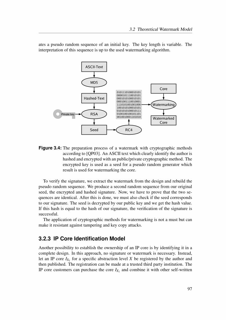
3.2 Theoretical Watermark Model
ates a pseudo random sequence of an initial key. The key length is variable. Theinterpretation of this sequence is up to the used watermarking algorithm.
ASCII-Text
MD5
Hashed-Text
RSA
010111010001010100001011100101010001010100010101000100111001000111101010010010001001010100010101010101010001011101001001001011010010010001101010
Private key
Seed RC4
Watermarking
Core
WatermarkedCore
Figure 3.4: The preparation process of a watermark with cryptographic methodsaccording to [QP03]. An ASCII text which clearly identify the author ishashed and encrypted with an public/private cryptographic method. Theencrypted key is used as a seed for a pseudo random generator whichresult is used for watermarking the core.
To verify the signature, we extract the watermark from the design and rebuild thepseudo random sequence. We produce a second random sequence from our originalseed, the encrypted and hashed signature. Now, we have to prove that the two se-quences are identical. After this is done, we must also check if the seed correspondsto our signature. The seed is decrypted by our public key and we get the hash value.If this hash is equal to the hash of our signature, the verification of the signature issuccessful.
The application of cryptographic methods for watermarking is not a must but canmake it resistant against tampering and key copy attacks.
3.2.3 IP Core Identification Model
Another possibility to establish the ownership of an IP core is by identifying it in acomplete design. In this approach, no signature or watermark is necessary. Instead,let an IP core IX1 for a specific abstraction level X be registered by the author andthen published. The registration can be made at a trusted third party institution. TheIP core customers can purchase the core IX1 and combine it with other self-written
97
3. IP Core Watermarking and Identification
or purchased IP cores IX2, IX3, . . . , IXm to a complete design which traverses furtherdesign steps to lower abstraction levels: IY = TX→Y (IX1 IX2 IX3 · · · IXm). The operator combines different cores to one design. If a company is suspected to usean unlicensed core, their design can be analyzed in a way that the unlicensed IP coreusage can be detected. This can be done by an IP core detector D which is able todetect the published IP core in a complete design: D(IY , IX1) = true/ f alse.
The threat and attack model against proof of authorship using IP core identificationmethods differ slightly from the threat and attack model when using watermarked IPcores. An attacker can try to achieve an ownership deadlock by using an ambiguityattack. He can claim that an identified IP core IX1 belongs to him. To prove his claim,he can further present the original IP core IX1 which he used to build his completedesign. This core can be obtained or purchased from the IP core developer or anyother source (e.g., legal customers of the core which copy the core). Since the IPcore IX1 has no signature, the real author cannot be determined. Only by using atrusted third party institute, the real owner of the IP core IX1 can be determined. Here,it is of utmost importance that the real owner of the core registered the IP core first.Usually, this should happen before the IP core is published. Furthermore, the attackercan take over the ownership of the core, if the original author forgot the registration.If the same IP core is registered at different trusted third party institutes, the date offiling should solve the dispute.
Furthermore, an attacker can counterfeit the ownership if he embeds a watermarkinside a copied core which identifies him as the legal author. This copy attack can beprevented if the core was previously registered at a trusted institution by the rightfulauthor. On the other hand, if an attacker registers a copied watermarked core at atrusted third party institution at which the work was not registered before, the estab-lishment of the ownership can be difficult. Because of the registered core carries al-ready the watermark, a judge would properly decide for the author of the watermark.This shows us that registration of an IP core at a trusted third party institute, even ifit is watermarked correctly, elevates the chances of the rightful proof of authorship.
In summary, it can be said that the clear proof of authorship using any identificationmethod can only be done if the IP core is registered. For watermarking methods, thisis not mandatory. However, registration can increase the trust into the ownershipproof significantly.
3.3 Bitfile Watermarking and Identification
This section explains methods where the verification is done by extracting an FPGAbitfile. The bitfile can be analyzed to detect structures that can carry a watermark orthat can be used to identify an IP core. In this work, lookup table contents are usedwhich are excellently suitable for watermarking and IP core identification.
98
3.3 Bitfile Watermarking and Identification
First of all, the extraction of the lookup table contents from an FPGA bitfile is dis-cussed. This step is necessary for all following IP core identification and bitfile water-marking methods. Afterwards, methods to identify a registered IP core in an FPGAbitfile are proposed. These include identifying netlist cores as well as HDL cores.Following, watermarking methods for netlist and bitfile cores are proposed. The fo-cus of these watermarking methods lies on the usage of functional lookup tables inorder to increase the robustness against removal attacks. The term functional lookuptable refers to lookup tables which are already used in a given (non-watermarked)IP core and represent a part of the functional logic of the core which may not beremoved by an attacker in order to retain the correctness of the core.
3.3.1 Lookup Table Content ExtractionIn this section, we discuss which possibilities exist to get information about the con-tents of lookup tables from a product. First, we need to extract the configurationbitfile of the FPGA from the product. On some devices, it is possible to read back thebitfile. This is the easiest way, but it is not always possible, because not all FPGAdevices support this feature, or it might have been disabled by the creator. In SRAMbased FPGAs, the bitfile is stored into a PROM and during the startup phase, theFPGA is configured by loading this bitfile. The communication between the FPGAand the PROM can be recorded by wire tapping and so, the bitfile can be obtained.
The extraction of the lookup table contents from the configuration bitfile dependson the FPGA device and the FPGA vendor. Xilinx provide the Java library JBits[Xilc] for Virtex-II FPGA configuration bitfiles. Although, all other Xilinx devicesmust be reversed engineered in order to obtain any information of their configurationbitfiles.
To read out the LUT content directly from the bitfile, it must be known at whichposition in the bitfile the lookup table content is stored and now these values must beinterpreted.
We have applied standard black-box reverse engineering procedures to Xilinx Vir-tex-II and Virtex-II Pro bitfiles. These bitfiles are structured in packets, where eachpacket consists of one or more configuration words for a certain configuration regis-ter which controls the configuration process [Xil05]. One large packet contains theconfiguration data for the circuit, which should be instantiated on the FPGA. Thispacket is divided into frames which are the smallest configuration unit. The lengthof one frame and the number of frames is device-dependent. There exist six frametypes: IOB, IOI, CLB, BRAM, BRAM Interconnect, and GCLK. In IOB (Input/Out-put Blocks) frames, the information about the right and left Input and Output Blocksis stored. The information about the upper and lower IOBs is stored in the CLB(Configurable Logic Block) frames. On the left and on the right side of the FPGAexists one column of IOB frames; each IOB column consists of four frames. TheIOI (Input/Output Interconnect) frames are next to the IOB frames. Here, the routing
99

3. IP Core Watermarking and Identification
information of the interconnect network for the IOBs is stored. There are also 22 IOIframes on each side of the FPGA. In the CLB frames, information about the CLBs,routing and the upper and lower IOBs are stored. The FPGA consists of a regularpattern of CLB columns. Each CLB column consists of 22 frames. In two of theseframes, the contents of the lookup tables are stored. In BRAM (Block Ram) and theBRAM Interconnect frames, the content and the configuration of the block rams aswell as the configuration of the hardware multiplier and the interconnect network isdeposited. Each BRAM column consists of 64 frames and each BRAM Interconnectcolumn consists of 22 frames. Each FPGA has one GCLK (Global Clock) column,consisting of four frames. Here, the information of DCMs (Digital Clock Manager),clock buffers and most of the clock routing is stored. More information can be foundin [Xil05].
Each frames of the configuration memory in the FPGA can be accessed by anindividual address. The address word contains a block address and a major and aminor address. The IOB, IOI, GCLK and CLB frames are stored in the block withaddress 0, whereas the BRAM frames are stored in the block with address 1. Block2 consists of the BRAM Interconnect frames. The major address directs the columnswhereas the minor address directs the frames in a column. Figure 3.5 shows theconfiguration map of a Xilinx Virtex-II or Virtex-II Pro FPGA. This is also the orderin which the frames are stored in the configuration packet in the bitfile.
Figure 3.5: The map of the configuration memory from Xilinx Virtex-II and Virtex-II Pro FPGAs [Xil05].
A Xilinx Virtex-II CLB consists of four slices, two horizontal and two vertical.Each slice has two lookup tables, the G- and the F-LUT. The content of the lookuptables for one slice column is stored in one frame, so two frames are used for thelookup table content in a CLB column. In the second frame of a CLB column, thelookup table content of the left slice column is stored whereas the third frame carriesthe content of the right slice column.
16 bits are stored in a four input lookup table. These bits are stored together in twobytes but with bit inverted values. The F and G lookup tables in a slice are separated
100
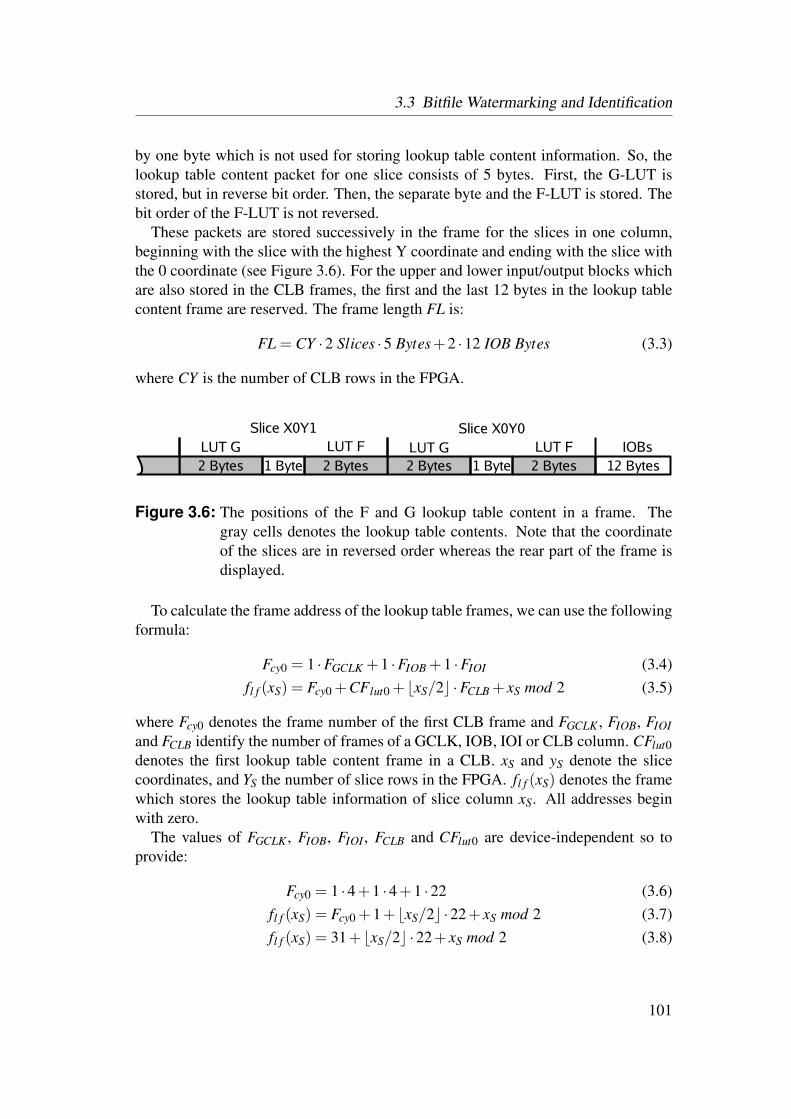
3.3 Bitfile Watermarking and Identification
by one byte which is not used for storing lookup table content information. So, thelookup table content packet for one slice consists of 5 bytes. First, the G-LUT isstored, but in reverse bit order. Then, the separate byte and the F-LUT is stored. Thebit order of the F-LUT is not reversed.
These packets are stored successively in the frame for the slices in one column,beginning with the slice with the highest Y coordinate and ending with the slice withthe 0 coordinate (see Figure 3.6). For the upper and lower input/output blocks whichare also stored in the CLB frames, the first and the last 12 bytes in the lookup tablecontent frame are reserved. The frame length FL is:
FL = CY ·2 Slices ·5 Bytes+2 ·12 IOB Bytes (3.3)
where CY is the number of CLB rows in the FPGA.
2 Bytes
Slice X0Y0
2 Bytes1 Byte 12 Bytes2 Bytes 2 Bytes1 ByteLUT FLUT G
Slice X0Y1LUT FLUT G IOBs
Figure 3.6: The positions of the F and G lookup table content in a frame. Thegray cells denotes the lookup table contents. Note that the coordinateof the slices are in reversed order whereas the rear part of the frame isdisplayed.
To calculate the frame address of the lookup table frames, we can use the followingformula:
Fcy0 = 1 ·FGCLK +1 ·FIOB +1 ·FIOI (3.4)fl f (xS) = Fcy0 +CFlut0 + bxS/2c ·FCLB + xS mod 2 (3.5)
where Fcy0 denotes the frame number of the first CLB frame and FGCLK , FIOB, FIOIand FCLB identify the number of frames of a GCLK, IOB, IOI or CLB column. CFlut0denotes the first lookup table content frame in a CLB. xS and yS denote the slicecoordinates, and YS the number of slice rows in the FPGA. fl f (xS) denotes the framewhich stores the lookup table information of slice column xS. All addresses beginwith zero.
The values of FGCLK , FIOB, FIOI , FCLB and CFlut0 are device-independent so toprovide:
Fcy0 = 1 ·4+1 ·4+1 ·22 (3.6)fl f (xS) = Fcy0 +1+ bxS/2c ·22+ xS mod 2 (3.7)fl f (xS) = 31+ bxS/2c ·22+ xS mod 2 (3.8)
101
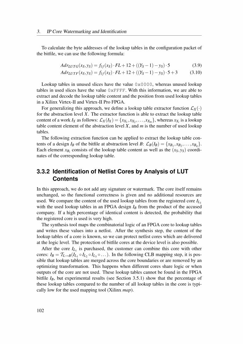
3. IP Core Watermarking and Identification
To calculate the byte addresses of the lookup tables in the configuration packet ofthe bitfile, we can use the following formula:
AdrLUT G(xS,yS) = fl f (xS) ·FL+12+((YS−1)− yS) ·5 (3.9)AdrLUT F(xS,yS) = fl f (xS) ·FL+12+((YS−1)− yS) ·5+3 (3.10)
Lookup tables in unused slices have the value 0x0000, whereas unused lookuptables in used slices have the value 0xFFFF. With this information, we are able toextract and decode the lookup table content and the position from used lookup tablesin a Xilinx Virtex-II and Virtex-II Pro FPGA.
For generalizing this approach, we define a lookup table extractor function LX(·)for the abstraction level X . The extractor function is able to extract the lookup tablecontent of a work IX as follows: LX(IX) = xX1,xX2, . . . ,xXm, whereas xXi is a lookuptable content element of the abstraction level X , and m is the number of used lookuptables.
The following extraction function can be applied to extract the lookup table con-tents of a design IB of the bitfile at abstraction level B: LB(IB) = xB1 ,xB2, . . . ,xBq.Each element xBi consists of the lookup table content as well as the (xS,yS) coordi-nates of the corresponding lookup table.
3.3.2 Identification of Netlist Cores by Analysis of LUTContents
In this approach, we do not add any signature or watermark. The core itself remainsunchanged, so the functional correctness is given and no additional resources areused. We compare the content of the used lookup tables from the registered core IL1
with the used lookup tables in an FPGA design IB from the product of the accusedcompany. If a high percentage of identical content is detected, the probability thatthe registered core is used is very high.
The synthesis tool maps the combinatorial logic of an FPGA core to lookup tablesand writes these values into a netlist. After the synthesis step, the content of thelookup tables of a core is known, so we can protect netlist cores which are deliveredat the logic level. The protection of bitfile cores at the device level is also possible.
After the core IL1 is purchased, the customer can combine this core with othercores: IB = TL→B(IL1 IL2 IL3 . . .). In the following CLB mapping step, it is pos-sible that lookup tables are merged across the core boundaries or are removed by anoptimizing transformation. This happens when different cores share logic or whenoutputs of the core are not used. These lookup tables cannot be found in the FPGAbitfile IB, but experimental results (see Section 3.5.1) show that the percentage ofthese lookup tables compared to the number of all lookup tables in the core is typi-cally low for the used mapping tool (Xilinx map).
102
3.3 Bitfile Watermarking and Identification
If a company is accused of using unlicensed cores in a product, the bitfile of theused FPGA can be extracted (see Section 3.3.1). After reading out the content and thepositions of the lookup tables from the bitfile and comparing them with the lookuptable contents from the original core, the ownership of the core can be proven byevaluating a detector function D(IB, IL1).
Identifying the Core
After the extraction of the content of lookup tables from a bitfile, we can com-pare the obtained values with the information in the netlist. The extraction of alllookup table contents from a bitfile is done as described in Section 3.3.1: LB(IB) =xB1,xB2 , . . . ,xBq. The content of the lookup tables can easily be read out from anetlist file: LL(IL1) = xL1,xL2, . . . ,xLr. For example, in an EDIF netlist for Xil-inx FPGA devices, the lookup table contents appear after the INIT property for thelookup table instances. Unfortunately, the mapping tools do not necessarily adoptthese values. The mapping tool may merge lookup tables from different cores to-gether, convert one, two or three input lookup tables to four input lookup tables andpermute the inputs to achieve a better routing.
All lookup tables of an FPGA have nl inputs. On most FPGA architectures, lookuptables have nl = 4 inputs. In a core netlist, also lookup tables with less than nl inputsmay exist. These lookup tables must be mapped onto nl input lookup tables. Ifone input is unused, only half of the memory is needed to store the function andthe remaining space must be filled. In the case that a function uses less inputs thanthe underlying technology of the FPGA provides, it is desirable to turn the unusedinputs into don’t cares. Intuitively, this can be achieved rather easily by replicatingthe function table as it is demonstrated in Figure 3.7.
000001010011100101110111
01110111
00011011
0111
0111
LUT2 LUT3
i1i0 i2i1i0 o o
Figure 3.7: Converting a two input lookup table into a three input lookup table withunused input i2.
103
3. IP Core Watermarking and Identification
The mapping tool can permute the inputs of the lookup tables, for example, toachieve a better routing. In most FPGA architectures, the routing resources forlookup table inputs are not equal, and so a permutation of the lookup table inputscan lower the amount of used routing resources. Permutation of the inputs signifi-cantly alters the content of a lookup table. For nl inputs, nl! permutations exist andthus up to nl! different lookup table values for one so-called unique function. Tocompare the contents of the lookup table from the netlist and the bitfile, it must bechecked if one of these possible different lookup table values for one unique functionis equal to the value of the lookup table in the bitfile. This is done by creating a tablewith all possible values of lookup tables for all unique functions (see Figure 3.8).
maptable
BitfileDesign
unique functions
maptable
NetlistCore
Lookup table contents
unique functions
compare:r is sub-set of q?
Lookup table contents
yes/no
q r
Figure 3.8: Before the lookup table contents of the bitfile and the netlist are com-pared, they are mapped into unique functions.
Robustness Analysis
For robustness analysis against false positive detection, it is necessary to know howmany different functions can be realized by an nl input lookup table, if it is allowedto permute the inputs. This topic is related to the problems of Boolean matching andequivalence classes [Har65, Hut03, ZV96, DS99]. Boolean matching is a techniqueto check if two Boolean function are equal with respect to transformations (e.g., inputpermutations, input negotiation, output negotiation). Functions which are equivalent
104

3.3 Bitfile Watermarking and Identification
with respect to these transformations are in the same equivalence class. Our interestis on the equivalence class P which allows to permute the inputs of a function.
The number of different values which can be encoded in an nl-input lookup tableis 22nl . The number of equivalence classes P is smaller. Table 3.1 shows the numberof equivalence classes of functions with different amounts of inputs. These valueswere obtained by experimentation. Functions which have a constant output do notappear in a netlist, but the mapping tool can create such functions later to generate apower or ground signal. Nevertheless, we define the set of unique functions as the setof equivalence classes without the two constant functions.
Inputs nl equivalence classes P unique functions fu1 4 22 12 103 80 784 3984 39825 37333248 [Har65] 37333246
Table 3.1: The number of different equivalence classes P and unique functions.
In order to decide whether a certain core is instantiated inside an FPGA, we definetwo vectors q and r that contain all quantities of each unique function appearing inthe core IL1 (r) and the whole design (q) that may consist of multiple different cores.Also, the number of different unique functions, denoted with fu, is of interest (seeTable 3.1).
The unique function i is included ri times in the core IL1 and thus qi times in thedesign IB. Moreover, r is the number of all functions or lookup tables in the core,and q the number of lookup tables in the whole design. The vector r can be obtainedfrom the set of different unique functions of the netlist of the core IL1 and the vectorq can be created from the information of the lookup table content extraction from thebitfile IB. Let
r = (r1,r2,r3, · · · ,r fu), (3.11)q = (q1,q2,q3, · · · ,q fu), (3.12)
and
r = r1 + r2 + r3 + · · ·+ r fu, (3.13)q = q1 +q2 +q3 + · · ·+q fu . (3.14)
Now, we can define a necessary criterion for a core to exist in a design: If thenumber of each different unique function qi in q is greater or equal to ri in r, the coreis possibly included in the design:
∀i ∈ 1, · · · , fu : qi ≥ ri (3.15)
105
3. IP Core Watermarking and Identification
Also, if a high percentage of unique functions qi in q is lower than ri in r, we cancome to the conclusion that the core is most likely not included.
An important value is the probability pc for the false-positive detection that a coreis found in a design by chance but which has this core not included. This value shouldbe very low to obtain a high robustness of this method. The probability depends onq, r, fu, the core r and the probability distribution pq of the unique functions of thewhole design.
pq = (p1, p2, p3, · · · , p fu), (3.16)p1 + p2 + p3 + · · ·+ p fu = 1, (3.17)
where p1 is the appearance probability of the function 1 in the design q.First, we assume that q = r. This means that we calculate the probability that the
number of each unique function of q and r is equal. All lookup tables of r must bein q with the probability distribution pq. This can be calculated with the multinomialdistribution:
pc =(
rr1,r2,r3, · · · ,r fu
)· pr1
1 · pr22 · pr3
3 · . . . · pr fufu . (3.18)
If q > r, the core IL1 (r) is combined with other cores or logic in the design IB (q).For each possible combination from r with other cores, the appearance probabilitymust be calculated and summed up. The first question is how many combinations ofother cores (s) exist. This can be calculated with the formula of combination withrepetitions:
s =( fu +q− r−1)!(q− r)! · ( fu−1)!
(3.19)
Now, all possible combinations of functions in these cores are calculated and storedin a matrix A.
A =
a11 a12 . . . a1 fua21 a22 . . . a2 fu
...... . . . ...
as1 as2 . . . as fu
, (3.20)
∀i ∈ 1, · · · ,s : ai1 +ai2 + · · ·+ai fu = q− r (3.21)
For example, for fu = 2 and q− r = 3:
A =
0 31 22 13 0
(3.22)
106
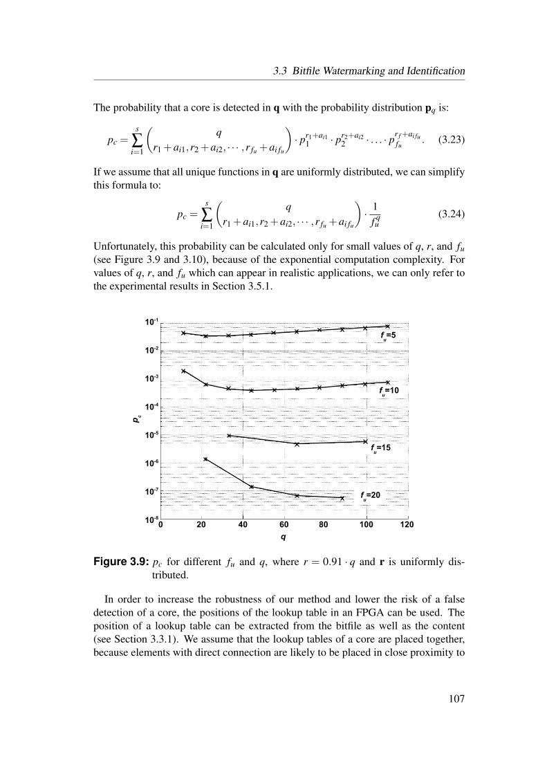
3.3 Bitfile Watermarking and Identification
The probability that a core is detected in q with the probability distribution pq is:
pc =s
∑i=1
(q
r1 +ai1,r2 +ai2, · · · ,r fu +ai fu
)· pr1+ai1
1 · pr2+ai22 · . . . · pr f +ai fu
fu . (3.23)
If we assume that all unique functions in q are uniformly distributed, we can simplifythis formula to:
pc =s
∑i=1
(q
r1 +ai1,r2 +ai2, · · · ,r fu +ai fu
)· 1
f qu
(3.24)
Unfortunately, this probability can be calculated only for small values of q, r, and fu(see Figure 3.9 and 3.10), because of the exponential computation complexity. Forvalues of q, r, and fu which can appear in realistic applications, we can only refer tothe experimental results in Section 3.5.1.
pc
q
4020 60 80 100 120
10-1
10-2
10-3
10-4
10-5
10-6
10-7
10-80
fu=5
fu=10
fu=15
fu=20
Figure 3.9: pc for different fu and q, where r = 0.91 · q and r is uniformly dis-tributed.
In order to increase the robustness of our method and lower the risk of a falsedetection of a core, the positions of the lookup table in an FPGA can be used. Theposition of a lookup table can be extracted from the bitfile as well as the content(see Section 3.3.1). We assume that the lookup tables of a core are placed together,because elements with direct connection are likely to be placed in close proximity to
107
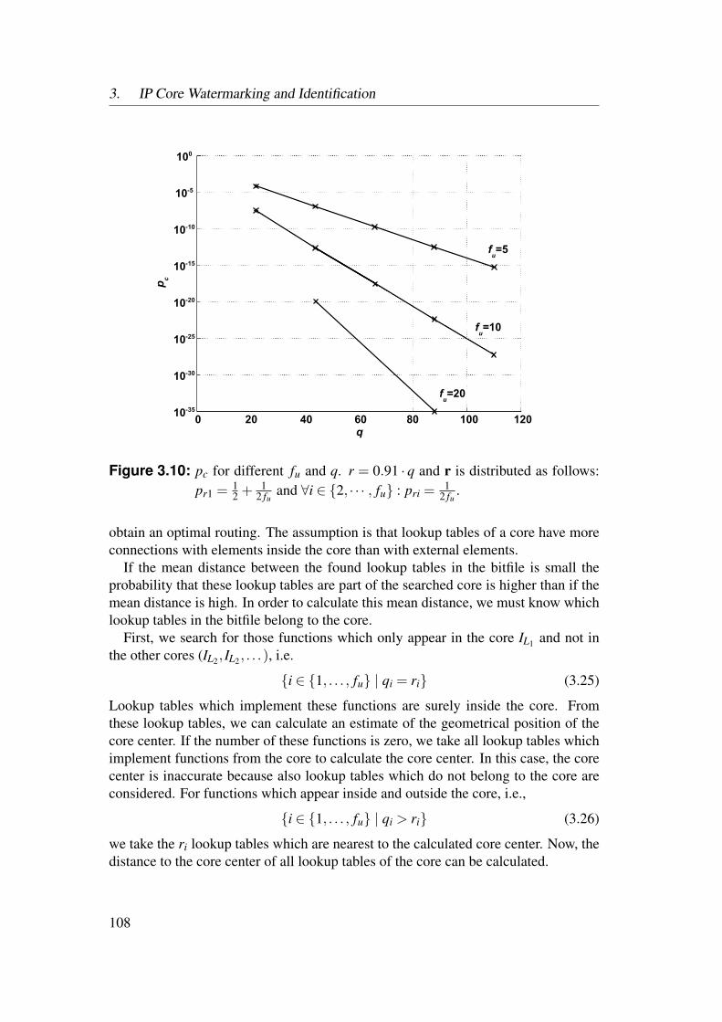
3. IP Core Watermarking and Identification
pc
q20 4020 60 80 100 120
100
10-5
10-10
10-15
10-20
10-25
10-30
10-350
fu=5
fu=10
fu=20
Figure 3.10: pc for different fu and q. r = 0.91 · q and r is distributed as follows:pr1 = 1
2 + 12 fu and ∀i ∈ 2, · · · , fu : pri = 1
2 fu .
obtain an optimal routing. The assumption is that lookup tables of a core have moreconnections with elements inside the core than with external elements.
If the mean distance between the found lookup tables in the bitfile is small theprobability that these lookup tables are part of the searched core is higher than if themean distance is high. In order to calculate this mean distance, we must know whichlookup tables in the bitfile belong to the core.
First, we search for those functions which only appear in the core IL1 and not inthe other cores (IL2 , IL2, . . .), i.e.
i ∈ 1, . . . , fu | qi = ri (3.25)
Lookup tables which implement these functions are surely inside the core. Fromthese lookup tables, we can calculate an estimate of the geometrical position of thecore center. If the number of these functions is zero, we take all lookup tables whichimplement functions from the core to calculate the core center. In this case, the corecenter is inaccurate because also lookup tables which do not belong to the core areconsidered. For functions which appear inside and outside the core, i.e.,
i ∈ 1, . . . , fu | qi > ri (3.26)
we take the ri lookup tables which are nearest to the calculated core center. Now, thedistance to the core center of all lookup tables of the core can be calculated.
108
3.3 Bitfile Watermarking and Identification
In the formula for pc, the difference between q and r is important. If q− r is small,then also the probability of a false detection pc is low. We can decrease q− r if wedefine a bounding box around the core and only consider lookup tables inside thebox. The dimensions of the box can be calculated from the positions of the lookuptables from the core inside the bitfile. However, the value of the probability pc mustbe multiplied with the number of all possible positions of the bounding box in thedesign.
Summary
We have presented a new method to identify IP cores in FPGA bitfiles. Possibletransformations of the mapping tools and the effect of the robustness of the methodwere discussed. The experimental results in Section 3.5.1 show that it is possible toidentify a core in the design with a high probability. The identification process isbased on two parameters, namely the number of found lookup tables of the core inthe design and the mean distance to the core center. However, it must be taken intoaccount that lookup tables of the core are removed by optimization tools, if parts ofthe core are not used because outputs are unused or constant values are applied toinputs.
3.3.3 Identification of HDL Cores by Analysis of LUTContents
In the last section we have shown that is possible to identify an IP core, distributedas a netlist, in an FPGA design by analyzing the LUT contents of the configurationbitfile. However, many IP cores are published at the RTL abstraction level as HDLcore.
To identify HDL cores, the lookup table contents can be used as well. However,the lookup table content is generated by the synthesis step, which is executed afterthe publication of the HDL cores. Therefore, a pirate who can obtain an unlicensedHDL core, controls the complete design flow from the RTL to the device level. Itis up to the pirate to decide which synthesis tool is used to synthesize the core andtherefore, create the lookup table contents. Different synthesis tools might createdifferent lookup table contents. To prove or disprove this assumption, we analyzedcommon synthesis tools with respect to the generation of lookup table contents.
The first step is to analyze different netlist cores to find out whether they weregenerated from the same HDL core. The goal is to find different netlist cores whichcan be assigned to a corresponding HDL source even if they were synthesized withdifferent tools and different synthesis parameters.
109
3. IP Core Watermarking and Identification
Criterion Value Method
To compare two netlist cores, we define the criterion value C. If this value is greaterthan 1, then it is likely that both netlist cores were generated from the same HDLsource. C is based on the lookup table content of both netlist cores. Therefore, thefirst step is to extract the lookup table contents from the netlist cores and map theseto unique functions. For one core, this step is the same procedure as in netlist coreidentification, described in Section 3.3.2. The procedure is done for both cores andthe results are two vectors which store the number of each unique function for thecorresponding core. ra is the vector of the first core ILA, and rb is the vector of thesecond core ILB:
ra = (ra1,ra2,ra3, · · · ,ra fu), ra =fu
∑i=1
rai, (3.27)
rb = (rb1,rb2,rb3, · · · ,rb fu), rb =fu
∑i=1
rbi. (3.28)
The number of lookup tables that can be found in both cores and, which implementthe same unique function can be calculated if we take the minimum for all elementsof both vectors:
rmin,i =min(rai,rbi), ∀i ∈ 1 . . . fu. (3.29)
The value Pa in b denotes the percentage of unique functions of ILA that can be foundin ILB. The value Pb in a is calculated vice versa:
Pa in b =fu
∑i=1
rmin,i
rb, (3.30)
Pb in a =fu
∑i=1
rmin,i
ra. (3.31)
Note that both values are not necessarily the same, because of the possibly differentnumber of used lookup tables or functions ra and rb. For example, if we comparea core with a large number of lookup tables with a core which has only few lookuptables, it is likely that the content of the few lookup tables of the second core is alsofound in the large core. Vice versa, however, the percentage of the found lookuptables should be very low.
If the number of used lookup tables differs extremely between the two cores, thenthe probability that both cores were generated from the same source is low. Weintroduce a parameter IP which indicates that the difference of the number of usedlookup tables of both cores is more than the average of used lookup tables:
110

3.3 Bitfile Watermarking and Identification
ravg =ra + rb
2, (3.32)
rdi f f = |ra− rb| , (3.33)
IP =
0, if rdi f f > ravg
1, if rdi f f ≤ ravg(3.34)
Now, we can calculate the criterion value C:
C = 25 · IP
(ravg
rdi f f
)2
·(
Pa in b− Pa in b +Pb in a
2
)2
+(
Pb in a− Pa in b +Pb in a
2
)2
(3.35)
This formula is derived from the experimental results in Section 3.5.2. If C > 1then the probability that both cores were generated from the same source is high, ifC < 1 it is rather unlikely that both cores are related.
Identification of Synthesis Tools
After the identification of netlist cores that have been generated from the same HDLsource, it is also of interest to identify the synthesis tool that was used to generatethe netlist. If it is possible to identify the used synthesis tool from the lookup tablecontents, the HDL core can be synthesized with the same tool. A comparison of thegenerated netlist core with the bitfile can possibly provide better identification result.The fact, that only a few synthesis tools exist for a certain technology simplifies theidentification of the synthesis tool as well as the used core.
The first step is to analyze netlists that were generated by different synthesis tools.We identify characteristic usage of special primitive cells, which can be found onlyin netlists which were synthesized by a certain tool. For example, in our analysisfor Virtex-II synthesis tools we found different implementations of a simple inverterfunction. On precision synthesis from Mentor Graphics an inverter is always imple-mented into a LUT1 or LUT1 L primitive cell, whereas the Xilinx Synthesis Tech-nology (XST) synthesis tool implements an inverter always as an INV primitive cell.Synplify Pro from Synopsis uses both implementations for an inverter. Furthermore,LUT D primitive cells which use the local and the normal lookup table output (see[Xilh]) exist only in netlists which were generated by the XST synthesis tool.
However, during the implementation of these cores into a bitfile, an INV primitivecell might also be implemented into a one-input lookup table, which removes thisspecial characteristic. Future research might find better characteristics for synthesistools which might still be present in the bitfile. Ideally, such characteristics should befound in lookup tables, which can be easily extracted.
111

3. IP Core Watermarking and Identification
Conclusions and Future Work
We have shown the first steps towards an identification of HDL cores in bitfiles. Weconcentrated on the synthesis step between the RTL and logic abstraction level andhave shown that it is possible to identify netlist cores that were generated from thesame HDL source. Furthermore, we have shown that it might be possible to identifythe synthesis tool a netlist was generated by. However, to build the complete chain foridentification of HDL cores from bitfiles some links are missing. Being able to iden-tify the synthesis tool helps for the identification, but even if the same tool is used, theresulting netlists may be different due to varying synthesis parameters. IdentifyingHDL cores in netlists has an inherent uncertainness comparable to the identificationof netlist cores in bitfiles. By combining both techniques the uncertainness can betoo high to give a trustful result. Nevertheless, this is an interesting topic for futureresearch.
3.3.4 Watermarks in LUTs for Bitfile Cores
In this section, we introduce our first watermarking technique for IP cores. The easi-est way to watermark an FPGA design is to place the watermarks into the bitfiles. Bit-files are very inflexible because they were specifically generated for a certain FPGAdevice type, however, it makes sense to sell bitfile IP cores for common developmentplatforms which carry the same FPGA type. Usually, a bitfile core is a whole designwhich is completely placed and routed and therefore ready to use. There also existpartial bitfiles which carry only one core. These partial bitfile cores can be com-bined into one FPGA which increases the flexibility of these cores and therefore mayincrease the trade possibilities.
In this approach, we hide our signature inside unused lookup tables. It is veryunlikely that a design or bitfile core uses all available lookup tables in an FPGA.Before a design reaches this limit, the routing resources are exhausted and the timingdegenerates rapidly. Therefore, many unused lookup tables exist in usual designs.On the other hand, lookup table content extraction is not difficult (see Section 3.3.1).Using lookup tables for hiding a watermark which are far away from the used ones,makes it easier for an attacker to identify and remove them. Even if an attacker isable to extract all lookup tables from a bitfile core, the lookup tables which carry thewatermark should not be suspicious.
In Xilinx devices, lookup tables are grouped together with flip-flops into slices. Aslice usually consists more than one lookup table, e.g., the Virtex-II and Virtex-II Prodevices which are discussed in Section 3.3.1, have two lookup tables in one slice.It is not unusual that only one lookup table of a slice is used and the other remainsunused. Hiding a watermark in the unused lookup table of a used slice is less obviousthan using lookup tables in unused slices. Even if the attacker is able to extract thelookup table content and coordinates, the watermarks are hard to detect.
112
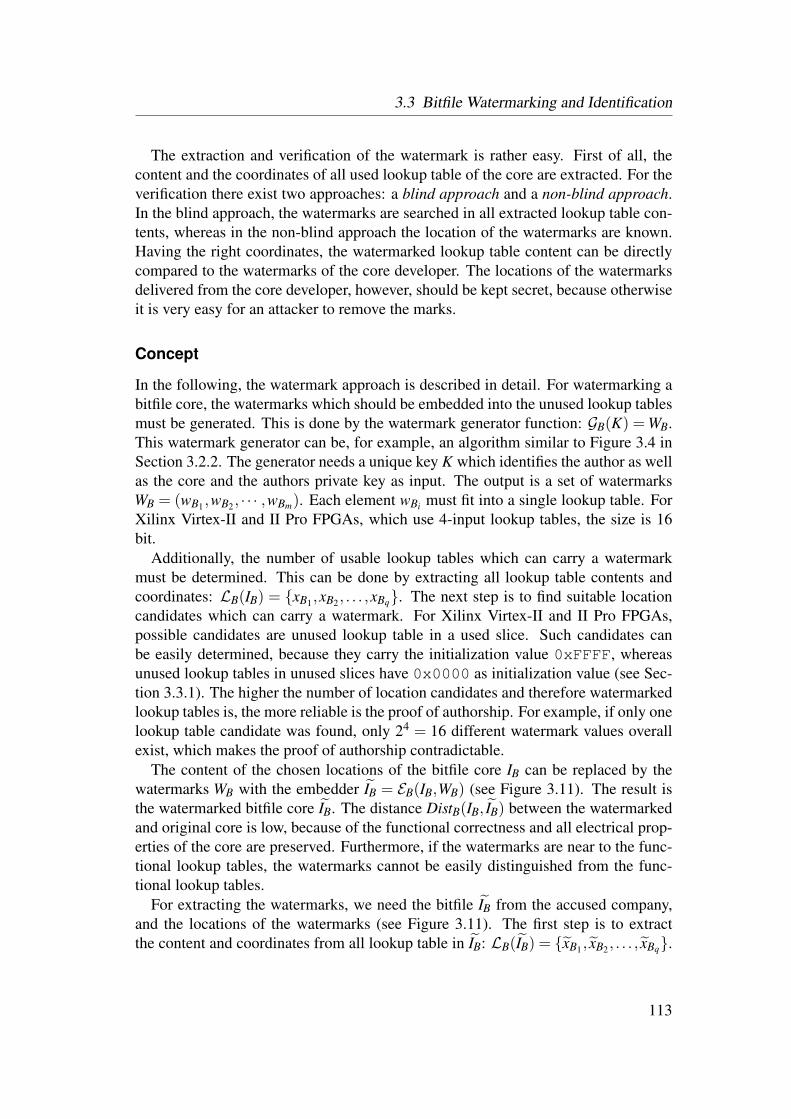
3.3 Bitfile Watermarking and Identification
The extraction and verification of the watermark is rather easy. First of all, thecontent and the coordinates of all used lookup table of the core are extracted. For theverification there exist two approaches: a blind approach and a non-blind approach.In the blind approach, the watermarks are searched in all extracted lookup table con-tents, whereas in the non-blind approach the location of the watermarks are known.Having the right coordinates, the watermarked lookup table content can be directlycompared to the watermarks of the core developer. The locations of the watermarksdelivered from the core developer, however, should be kept secret, because otherwiseit is very easy for an attacker to remove the marks.
Concept
In the following, the watermark approach is described in detail. For watermarking abitfile core, the watermarks which should be embedded into the unused lookup tablesmust be generated. This is done by the watermark generator function: GB(K) = WB.This watermark generator can be, for example, an algorithm similar to Figure 3.4 inSection 3.2.2. The generator needs a unique key K which identifies the author as wellas the core and the authors private key as input. The output is a set of watermarksWB = (wB1,wB2, · · · ,wBm). Each element wBi must fit into a single lookup table. ForXilinx Virtex-II and II Pro FPGAs, which use 4-input lookup tables, the size is 16bit.
Additionally, the number of usable lookup tables which can carry a watermarkmust be determined. This can be done by extracting all lookup table contents andcoordinates: LB(IB) = xB1 ,xB2, . . . ,xBq. The next step is to find suitable locationcandidates which can carry a watermark. For Xilinx Virtex-II and II Pro FPGAs,possible candidates are unused lookup table in a used slice. Such candidates canbe easily determined, because they carry the initialization value 0xFFFF, whereasunused lookup tables in unused slices have 0x0000 as initialization value (see Sec-tion 3.3.1). The higher the number of location candidates and therefore watermarkedlookup tables is, the more reliable is the proof of authorship. For example, if only onelookup table candidate was found, only 24 = 16 different watermark values overallexist, which makes the proof of authorship contradictable.
The content of the chosen locations of the bitfile core IB can be replaced by thewatermarks WB with the embedder IB = EB(IB,WB) (see Figure 3.11). The result isthe watermarked bitfile core IB. The distance DistB(IB, IB) between the watermarkedand original core is low, because of the functional correctness and all electrical prop-erties of the core are preserved. Furthermore, if the watermarks are near to the func-tional lookup tables, the watermarks cannot be easily distinguished from the func-tional lookup tables.
For extracting the watermarks, we need the bitfile IB from the accused company,and the locations of the watermarks (see Figure 3.11). The first step is to extractthe content and coordinates from all lookup table in IB: LB(IB) = xB1 , xB2, . . . , xBq.
113
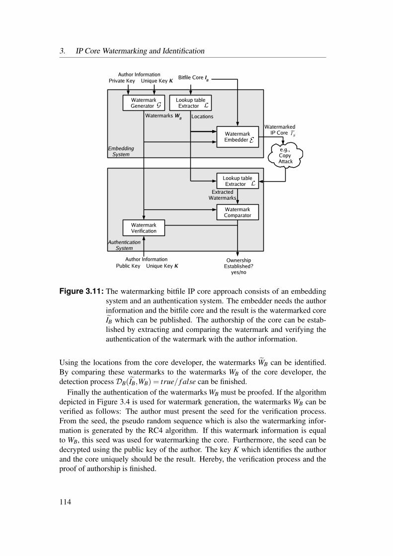
3. IP Core Watermarking and Identification
AuthenticationSystem
EmbeddingSystem
WatermarkGenerator
Watermarks WB
Unique Key K
WatermarkEmbedder
Private KeyAuthor Information
Lookup tableExtractor
Bitfile Core IB
Locations
e.g., Copy Attack
WatermarkedIP Core I B
Lookup tableExtractor
WatermarkComparator
ExtractedWatermarks
WatermarkVerification
Unique Key KPublic KeyAuthor Information Ownership
Established?yes/no
Figure 3.11: The watermarking bitfile IP core approach consists of an embeddingsystem and an authentication system. The embedder needs the authorinformation and the bitfile core and the result is the watermarked coreIB which can be published. The authorship of the core can be estab-lished by extracting and comparing the watermark and verifying theauthentication of the watermark with the author information.
Using the locations from the core developer, the watermarks WB can be identified.By comparing these watermarks to the watermarks WB of the core developer, thedetection process DB(IB,WB) = true/ f alse can be finished.
Finally the authentication of the watermarks WB must be proofed. If the algorithmdepicted in Figure 3.4 is used for watermark generation, the watermarks WB can beverified as follows: The author must present the seed for the verification process.From the seed, the pseudo random sequence which is also the watermarking infor-mation is generated by the RC4 algorithm. If this watermark information is equalto WB, this seed was used for watermarking the core. Furthermore, the seed can bedecrypted using the public key of the author. The key K which identifies the authorand the core uniquely should be the result. Hereby, the verification process and theproof of authorship is finished.
114

3.3 Bitfile Watermarking and Identification
Robustness Analysis
Attacks against the watermarking scheme are, according to Section 3.2.1, ambiguity,removal, and key copy attacks. The prevention of the copy attack, where an attackerwatermarks an IP core which he illegally obtained with his own signature, is almostimpossible. A possible solution of this dilemma is to watermark all published worksor register the core on a trusted third party institute.
In case of removal attacks, the attacker tries to remove the watermarks. If he knowsthe location of the watermarks this task is easy. Therefore, it is utmost important thatthe locations of the watermarked are kept secret. If the attacker does not know thelocations, he can try to analyze the bitfile. If he is only able to extract the lookup tablecontent and the locations of the lookup tables, it is almost impossible to detect thewatermark, because the locations are near the functional lookup tables and the contentis not distinguishable from the other lookup tables. However, if the attacker is able toreverse engineer the bitfile core to the logic level (IL = TL←B(IB)), the watermarks areeasy to detect and can be removed. This task is, however, very expensive if no reverseengineering tool is available. For Virtex-II devices the Xilinx “reverse engineering”tool JBits [Xilc] is available, which is in fact able to remove the watermarks.
The attacker may analyze the bitfile core and search for lookup table content whichhe can present as his own watermark in case of ambiguity attacks. He can use the in-serted watermarks and assert that these watermarks belong to him. To be successfulwith such an attack, he must also present the procedure to generate the watermarks.Hereby, the attacker must generate a signatures or key which identifies him as theauthor and fits to the watermarks inside the core. This is very hard to achieve due tothe usage of one way cryptographic functions. Furthermore, the attacker can presentsome functional lookup tables as his watermarks. This should also be nearly impossi-ble due to the characteristics of one way cryptographic functions. Another possibilityto check this attack, is to remove the watermarks from the bitfile core. The correctwatermarks are inserted after the implementation of the core and therefore the coreshould keep the functional correctness. Whereas the removal of the wrong water-marks which are functional lookup table contents, destroys the core.
Using asynchronous public/private key cryptographic functions for the watermarkgeneration and verification and further storing information about the core into theunique key successfully prevents key copy attacks.
3.3.5 Watermarks in Functional LUTs for Netlist Cores
After watermarking bitfile cores, we now watermark netlist cores. Netlist IP coresconsist of primitive cells (e.g., LUT4, DFF, XORCY) of a certain FPGA family whichcovers many different FPGA devices. For example, the whole Xilinx Virtex-4, orAltera Stratix-II family with all different FPGA sizes. This means, that one netlistcore can be deployed for the whole family without changing the file. Once again,
115

3. IP Core Watermarking and Identification
we are using the Virtex-II and II Pro family to demonstrate this approach. However,using other FPGA families should also be possible by adapting the methods to theirprimitive cells. Another big advantage from netlist cores over bitfile cores is that thebitfile creator (e.g., product developer) can combine different cores.
As mentioned before in Section 3.3.2, FPGAs usually consist of the same type oflookup tables with regard to the number of inputs. For example, the Xilinx Virtex-IIuses lookup tables with four inputs whereas the Virtex-5 has lookup tables with sixinputs. However, in common netlist cores many logical lookup tables exist, whichhave less inputs than the FPGA type. These lookup tables are mapped to the physicallookup tables of the FPGA. If the logical lookup table of the netlist cores has fewerinputs than the physical one, the memory space which cannot be addressed remainsunused. We use this memory space to embed a watermark into functional lookuptables.
One problem of watermarking netlist cores is that the core further traverses the de-sign flow which includes different optimization steps. Additive watermarking meth-ods which use redundant structures or logic as watermark have the problem that theglobal optimization steps may detect and remove this redundancy. Todays designtools are very sophisticated to find redundant logic in a design. Even if a special re-dundant logic which can be used as watermark is not removed by today’s tools, it isnot granted that future versions or other tools may not detect and remove this logic.The challenge is to find an element or component which can be used as watermarkand is not altered by design tools. For Xilinx FPGAs such elements are shift registersand memories which are implemented in lookup tables.
In some FPGA architectures (e.g., all Xilinx Virtex architectures), the lookup ta-bles (LUTs) can also be used as a shift register or distrubuted memory [Xilf]. Forexample, a 4-input lookup table can be further used as a 16-bit shift register (see Fig-ure 3.12). The content of such a shift register can be further addressed by the lookuptable input ports. So, the shift register can also be used as a functional lookup table. Ifthe lookup table is used as a LUT primitive cell, the content is interpreted as logic bythe design tools and is in focus of optimization. However, if the same content is usedas a shift register or memory primitive cell, the design tools do not touch the con-tent. Using the unused memory space of functional lookup tables for watermarkingwithout converting the lookup table either to a shift register or distributed memoryturns out to be not applicable, because design flow tools identify the watermark asredundant and remove the content due to optimization. Converting the watermarkedfunctional lookup table into shift registers or memory cells, prevents the watermarkfrom deletion due to optimization.
Embedding of the Watermark
In this approach we are use Virtex-II Pro FPGAs and convert LUT1, LUT2, or LUT3primitive cell which can be found in netlists of IP cores into the shift register primitive
116

3.3 Bitfile Watermarking and Identification
A1A2A3A4
CKEN
D
Q
Q15
SRL16A1A2A3A4
CKEN
D
Q
Q15
LUT4
Figure 3.12: In the Xilinx Virtex architecture, a lookup table (LUT4) can also beconfigured as a 16-bit shift register (SRL16).
cell SRLC16E. Note that LUT1 has one input, LUT2 two and so on. LUT4 has fourinput and uses the whole lookup table memory for its function which make this typeuninteresting for our approach. The content of the physical 4-input lookup table inan FPGA stores 16 bits. A LUT3 primitive cell uses only 8 bits, a LUT2 4 bits,and LUT1 only 2 bits out of the 16 bits. The Xilinx mapping tool map duplicatesthe used memory area to the unused area if not all inputs are needed (see Section3.3.2). Therefore, to use the unused memory space for embedding a watermark, wemust restrict the memory reachability of the function by clamping the unused inputsto constant values. In Figure 3.13, we demonstrate this idea for an AND-function,implemented by a LUT2. By clamping input A3 and A4 to zero, we can free 12 bitswhich can be used for carrying a watermark.
0 0 1
0 0 0 1 ? ? ? ? ? ? ? ? ? ? ? ?
A1A2A3A4
O
A4 <= '0'
A3 <= '0' Free space for watermark
0 0 0 0 0 0 1 1 1 1 1 1 10 0 0 0 1 1 1 1 0 0 0 0 1 1 1 10 0 1 1 0 0 1 1 0 0 1 1 0 0 1 10 1 0 1 0 1 0 1 0 1 0 1 0 1 0 1
O <= A1 and A2
Figure 3.13: Example of implementing a two input AND gate using a four inputlookup table. Addressable storage is restricted by connecting the un-used inputs to zero [SZT08].
117
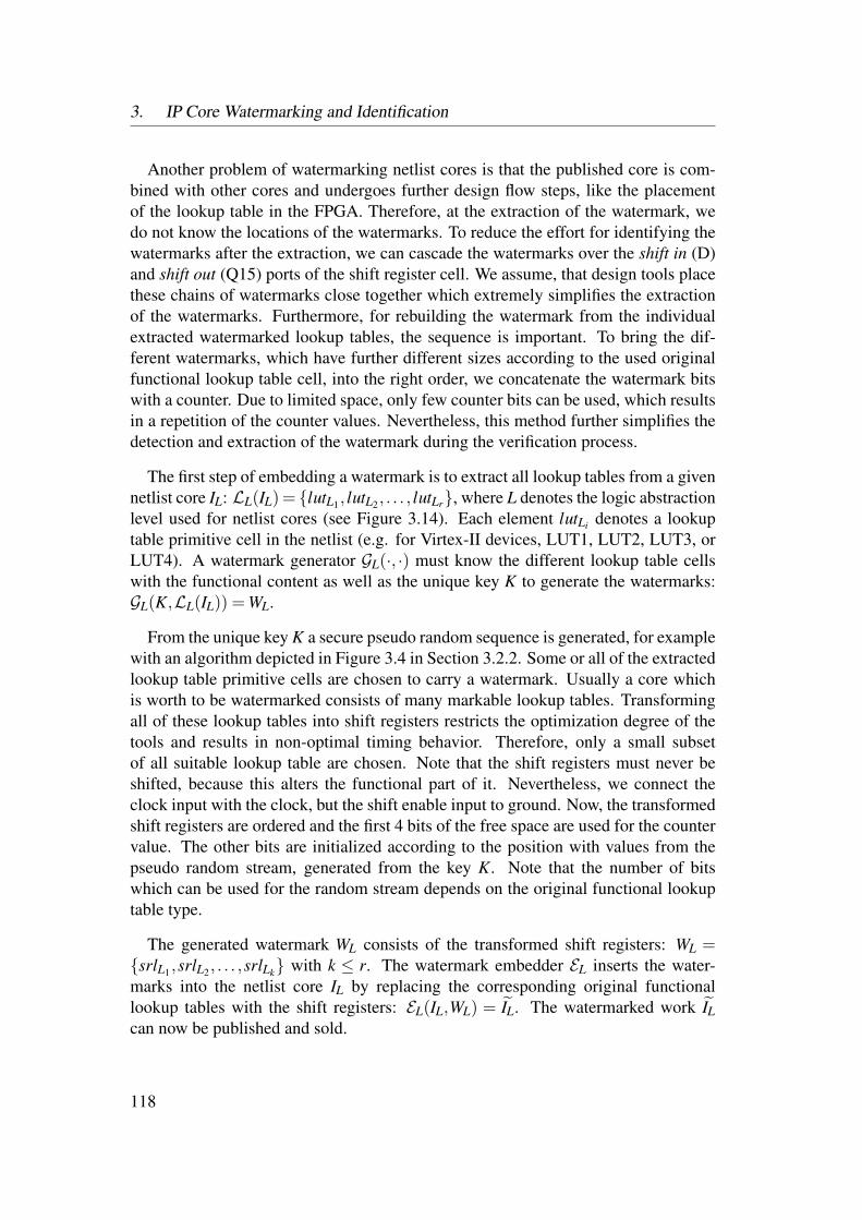
3. IP Core Watermarking and Identification
Another problem of watermarking netlist cores is that the published core is com-bined with other cores and undergoes further design flow steps, like the placementof the lookup table in the FPGA. Therefore, at the extraction of the watermark, wedo not know the locations of the watermarks. To reduce the effort for identifying thewatermarks after the extraction, we can cascade the watermarks over the shift in (D)and shift out (Q15) ports of the shift register cell. We assume, that design tools placethese chains of watermarks close together which extremely simplifies the extractionof the watermarks. Furthermore, for rebuilding the watermark from the individualextracted watermarked lookup tables, the sequence is important. To bring the dif-ferent watermarks, which have further different sizes according to the used originalfunctional lookup table cell, into the right order, we concatenate the watermark bitswith a counter. Due to limited space, only few counter bits can be used, which resultsin a repetition of the counter values. Nevertheless, this method further simplifies thedetection and extraction of the watermark during the verification process.
The first step of embedding a watermark is to extract all lookup tables from a givennetlist core IL: LL(IL) = lutL1, lutL2, . . . , lutLr, where L denotes the logic abstractionlevel used for netlist cores (see Figure 3.14). Each element lutLi denotes a lookuptable primitive cell in the netlist (e.g. for Virtex-II devices, LUT1, LUT2, LUT3, orLUT4). A watermark generator GL(·, ·) must know the different lookup table cellswith the functional content as well as the unique key K to generate the watermarks:GL(K,LL(IL)) = WL.
From the unique key K a secure pseudo random sequence is generated, for examplewith an algorithm depicted in Figure 3.4 in Section 3.2.2. Some or all of the extractedlookup table primitive cells are chosen to carry a watermark. Usually a core whichis worth to be watermarked consists of many markable lookup tables. Transformingall of these lookup tables into shift registers restricts the optimization degree of thetools and results in non-optimal timing behavior. Therefore, only a small subsetof all suitable lookup table are chosen. Note that the shift registers must never beshifted, because this alters the functional part of it. Nevertheless, we connect theclock input with the clock, but the shift enable input to ground. Now, the transformedshift registers are ordered and the first 4 bits of the free space are used for the countervalue. The other bits are initialized according to the position with values from thepseudo random stream, generated from the key K. Note that the number of bitswhich can be used for the random stream depends on the original functional lookuptable type.
The generated watermark WL consists of the transformed shift registers: WL =srlL1,srlL2 , . . . ,srlLk with k ≤ r. The watermark embedder EL inserts the water-marks into the netlist core IL by replacing the corresponding original functionallookup tables with the shift registers: EL(IL,WL) = IL. The watermarked work ILcan now be published and sold.
118
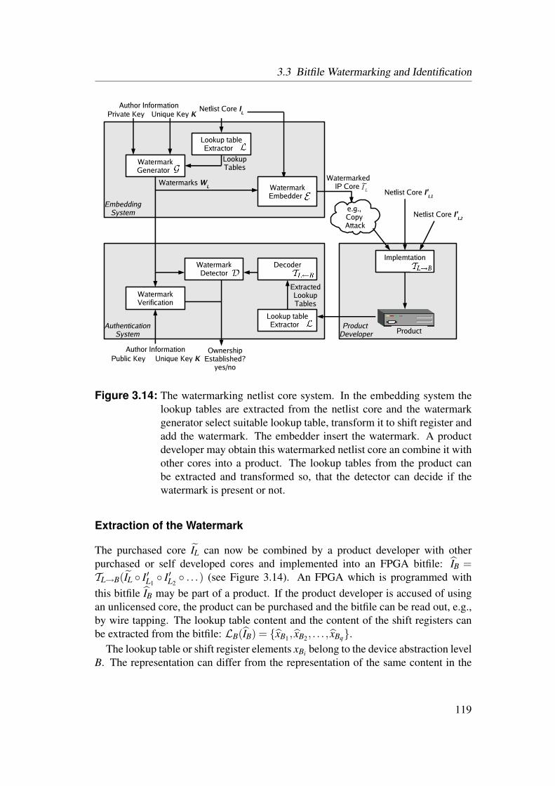
3.3 Bitfile Watermarking and Identification
Product Developer
AuthenticationSystem
EmbeddingSystem
WatermarkGenerator
Watermarks WL
Unique Key K
WatermarkEmbedder
Private KeyAuthor Information
Lookup tableExtractor
Netlist Core IL
LookupTables
e.g., Copy Attack
WatermarkedIP Core I L
Lookup tableExtractor
WatermarkDetector
ExtractedLookup Tables
WatermarkVerification
Unique Key KPublic KeyAuthor Information Ownership
Established?yes/no
Implemtation
Netlist Core I'L1
Netlist Core I'L2
Decoder
Product
Figure 3.14: The watermarking netlist core system. In the embedding system thelookup tables are extracted from the netlist core and the watermarkgenerator select suitable lookup table, transform it to shift register andadd the watermark. The embedder insert the watermark. A productdeveloper may obtain this watermarked netlist core an combine it withother cores into a product. The lookup tables from the product canbe extracted and transformed so, that the detector can decide if thewatermark is present or not.
Extraction of the Watermark
The purchased core IL can now be combined by a product developer with otherpurchased or self developed cores and implemented into an FPGA bitfile: IB =TL→B(IL I′L1
I′L2 . . .) (see Figure 3.14). An FPGA which is programmed with
this bitfile IB may be part of a product. If the product developer is accused of usingan unlicensed core, the product can be purchased and the bitfile can be read out, e.g.,by wire tapping. The lookup table content and the content of the shift registers canbe extracted from the bitfile: LB(IB) = xB1, xB2, . . . , xBq.
The lookup table or shift register elements xBi belong to the device abstraction levelB. The representation can differ from the representation of the same content in the
119
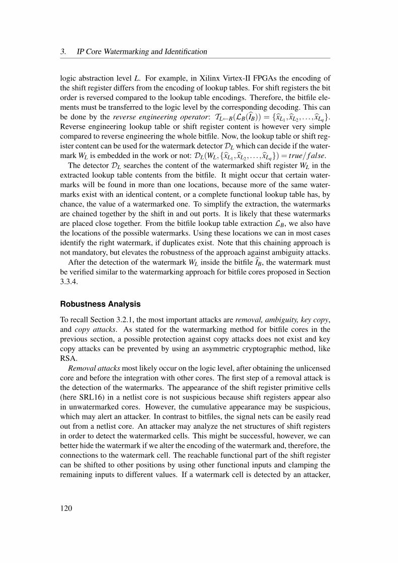
3. IP Core Watermarking and Identification
logic abstraction level L. For example, in Xilinx Virtex-II FPGAs the encoding ofthe shift register differs from the encoding of lookup tables. For shift registers the bitorder is reversed compared to the lookup table encodings. Therefore, the bitfile ele-ments must be transferred to the logic level by the corresponding decoding. This canbe done by the reverse engineering operator: TL←B(LB(IB)) = xL1, xL2, . . . , xLq.Reverse engineering lookup table or shift register content is however very simplecompared to reverse engineering the whole bitfile. Now, the lookup table or shift reg-ister content can be used for the watermark detectorDL which can decide if the water-mark WL is embedded in the work or not: DL(WL,xL1, xL2, . . . , xLq) = true/ f alse.
The detector DL searches the content of the watermarked shift register WL in theextracted lookup table contents from the bitfile. It might occur that certain water-marks will be found in more than one locations, because more of the same water-marks exist with an identical content, or a complete functional lookup table has, bychance, the value of a watermarked one. To simplify the extraction, the watermarksare chained together by the shift in and out ports. It is likely that these watermarksare placed close together. From the bitfile lookup table extraction LB, we also havethe locations of the possible watermarks. Using these locations we can in most casesidentify the right watermark, if duplicates exist. Note that this chaining approach isnot mandatory, but elevates the robustness of the approach against ambiguity attacks.
After the detection of the watermark WL inside the bitfile IB, the watermark mustbe verified similar to the watermarking approach for bitfile cores proposed in Section3.3.4.
Robustness Analysis
To recall Section 3.2.1, the most important attacks are removal, ambiguity, key copy,and copy attacks. As stated for the watermarking method for bitfile cores in theprevious section, a possible protection against copy attacks does not exist and keycopy attacks can be prevented by using an asymmetric cryptographic method, likeRSA.
Removal attacks most likely occur on the logic level, after obtaining the unlicensedcore and before the integration with other cores. The first step of a removal attack isthe detection of the watermarks. The appearance of the shift register primitive cells(here SRL16) in a netlist core is not suspicious because shift registers appear alsoin unwatermarked cores. However, the cumulative appearance may be suspicious,which may alert an attacker. In contrast to bitfiles, the signal nets can be easily readout from a netlist core. An attacker may analyze the net structures of shift registersin order to detect the watermarked cells. This might be successful, however, we canbetter hide the watermark if we alter the encoding of the watermark and, therefore, theconnections to the watermark cell. The reachable functional part of the shift registercan be shifted to other positions by using other functional inputs and clamping theremaining inputs to different values. If a watermark cell is detected by an attacker,
120

3.3 Bitfile Watermarking and Identification
he cannot easily remove the cell, because the cell also has a functional part. Byremoving the cell, the functional part is removed and the core is damaged. Therefore,after the detection of the watermark, the attacker must either decode the content of thewatermarked shift register to extract the functional part and insert a new lookup table,or overwrite the watermarked part of the cell with other values, so the watermark isnot detectable any more. The different encodings of the functional part of the shiftregister content complicates the analysis and the extraction of it. Furthermore, evenif some watermarks are removed, the establishment of the right ownership of the coreis still possible, because we need not all watermarked cells for a successful detectionof the signature.
In case of ambiguity attacks, an attacker analyzes the bitfile or the netlist to findshift register or lookup table contents which may be suitable to build a fake water-mark. Like the watermarking method for bitfile cores, the attacker must also presentthe insertion procedure to achieve a meaningful result. Due to the usage of secure oneway cryptographic functions for generating the watermark, the probability of a suc-cess is very low. Furthermore, the attacker can use a self-written netlist core which hewatermarked with his signatures and combine it with the obtained unlicensed core.The result is, that the watermarks of the authors of both cores are found in the bitfile,which are both trustful. Inside the unique key K, not only the author informationshould be included but also information of the core, e.g., a hash value over the netlistcore file without the watermark. Of course, the attacker can use the identification ofthe obtained unlicensed core for watermarking his core. However, to generate a hashvalue of the obtained core without watermarks, he must first remove the marks. Ingeneral, attacks against this approach are possible, but they need a high amount ofeffort. To increase the security against ambiguity attacks, the core may be registeredat a trusted third party.
Summary
In this section we presented a watermark method, which is able to watermark netlistcores. The netlist cores can be combined with other cores to assemble a productin an uncontrolled area from the core developer’s point of view. Nevertheless, thewatermark can be extracted from a bitfile which is recovered from a product from anaccused company. We have shown that the approach is resistant against removal andambiguity attacks.
The disadvantage of this approach is that we might have some timing overhead dueto the conversion of lookup tables to shift registers. As mentioned before, design toolscan permute inputs to achieve a better timing behavior. By converting the lookuptables into shift registers we take this optimization degree away from the tools, whichmay results in a worse timing. Experimental results of the timing overhead can befound in Section 3.5.4.
121

3. IP Core Watermarking and Identification
3.4 Power WatermarkingThis section introduces watermarking techniques, where a signature is verified overthe power consumption pattern of an FPGA. These techniques may also be suitablefor ASIC designs, however, we concentrate on FPGA designs and develop severalenhancements which are exclusively related to the FPGA technology. The presentedidea is new and differs from [KJJ99] and [AARR03] where the goal of using poweranalysis techniques is the detection of cryptographic keys and other security issues.
For power watermarking methods, the term signature refers to the part of the wa-termark which can be extracted and is needed for the detection and verification of thewatermark. The signature is usually a bit sequence which is derived from the uniquekey for author and core identification.
First of all, a short introduction is given and the communication channel betweenthe generation and the detection of the watermark is discussed. Next, the basismethod is presented and afterwards, several enhanced methods which increase therobustness of decoding the watermark in case of external or internal disturbances areintroduced. Finally, multiplex methods are discussed which enable the detection ofmore than one watermark if multiple watermarked cores are present in the design.
3.4.1 Verification over Power Consumption
There is no way to measure the relative power consumption of an FPGA directly,only through measuring the relative supply voltage or current. We have decided tomeasure the voltage of the core as close as possible to the voltage supply pins suchthat the smoothing from the plane and block capacities are minimal and no shunt isrequired. Most FPGAs have ball grid array (BGA) packages and the majority ofthem have vias to the back of the PCB for the supply voltage pins. So, the voltagecan be measured on the rear side of the PCB using an oscilloscope. The voltage canbe sampled using a standard oscilloscope, and analyzed and decoded using a programdeveloped to run on a PC. The decoded signature can be compared with the originalsignature and thus, the watermark can be verified. This method has the advantageof being non-destructive and requires no further information or aids than the givenproduct (see Figure 3.15).
The consumed power of an FPGA can be divided into two parts, namely the staticand the dynamic power. The static power consumption is caused by the leakage cur-rent from CMOS transistors and does not change over time if the temperature staysconstant. The dynamic power consists of the power related to short circuit currentsand the power required of reloading the capacities of transistors and wires. The shortcircuit current occurs when the PMOS and the NMOS transistors are both in conduct-ing state for a short time during the switching activity. As shown in [SKB02], themain part of an FPGA’s dynamic power results from capacity reloading. Both partsof the dynamic power consumption depend on the switching frequency [CSB92].
122
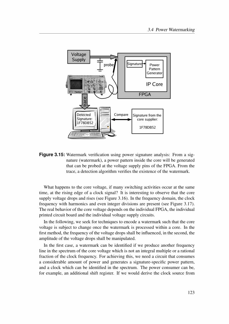
3.4 Power Watermarking
FPGA
Signature PowerPattern
Generator
VoltageSupply
trac
e
DetectedSignature:1F78DB52
Signature from the core supplier:
1F78DB52
Compare
probe
IP Core
Figure 3.15: Watermark verification using power signature analysis: From a sig-nature (watermark), a power pattern inside the core will be generatedthat can be probed at the voltage supply pins of the FPGA. From thetrace, a detection algorithm verifies the existence of the watermark.
What happens to the core voltage, if many switching activities occur at the sametime, at the rising edge of a clock signal? It is interesting to observe that the coresupply voltage drops and rises (see Figure 3.16). In the frequency domain, the clockfrequency with harmonics and even integer divisions are present (see Figure 3.17).The real behavior of the core voltage depends on the individual FPGA, the individualprinted circuit board and the individual voltage supply circuits.
In the following, we seek for techniques to encode a watermark such that the corevoltage is subject to change once the watermark is processed within a core. In thefirst method, the frequency of the voltage drops shall be influenced, in the second, theamplitude of the voltage drops shall be manipulated.
In the first case, a watermark can be identified if we produce another frequencyline in the spectrum of the core voltage which is not an integral multiple or a rationalfraction of the clock frequency. For achieving this, we need a circuit that consumesa considerable amount of power and generates a signature-specific power pattern,and a clock which can be identified in the spectrum. The power consumer can be,for example, an additional shift register. If we would derive the clock source from
123
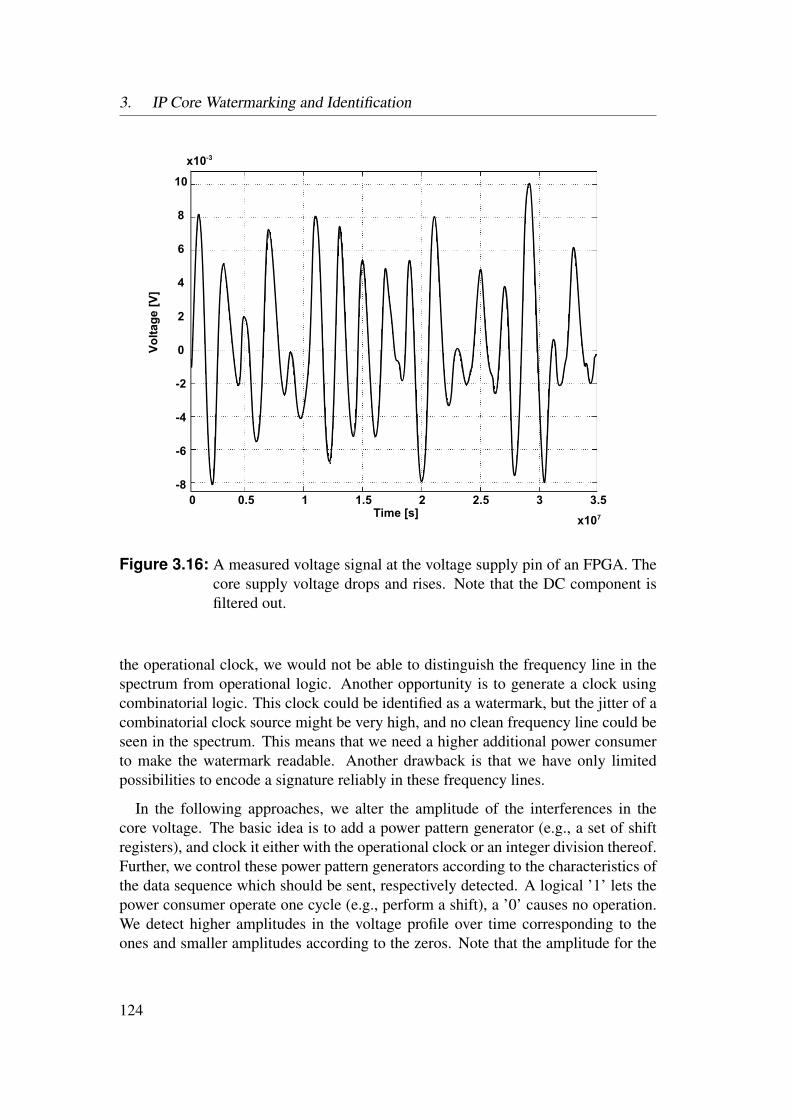
3. IP Core Watermarking and Identification
Vo
ltag
e [V
]
10.5 1.5 2.5 3.5-8
0 2 3Time [s]
x107
-6
-4
-2
0
2
4
6
8
10
x10-3
Figure 3.16: A measured voltage signal at the voltage supply pin of an FPGA. Thecore supply voltage drops and rises. Note that the DC component isfiltered out.
the operational clock, we would not be able to distinguish the frequency line in thespectrum from operational logic. Another opportunity is to generate a clock usingcombinatorial logic. This clock could be identified as a watermark, but the jitter of acombinatorial clock source might be very high, and no clean frequency line could beseen in the spectrum. This means that we need a higher additional power consumerto make the watermark readable. Another drawback is that we have only limitedpossibilities to encode a signature reliably in these frequency lines.
In the following approaches, we alter the amplitude of the interferences in thecore voltage. The basic idea is to add a power pattern generator (e.g., a set of shiftregisters), and clock it either with the operational clock or an integer division thereof.Further, we control these power pattern generators according to the characteristics ofthe data sequence which should be sent, respectively detected. A logical ’1’ lets thepower consumer operate one cycle (e.g., perform a shift), a ’0’ causes no operation.We detect higher amplitudes in the voltage profile over time corresponding to theones and smaller amplitudes according to the zeros. Note that the amplitude for the
124

3.4 Power Watermarking
50 15000 100
Frequency [Hz] x106
1000
150
2000
3000
4000
5000
6000
7000
8000
Am
plit
ud
e
Figure 3.17: The spectrum of the measured signal in Figure 3.16. The clock fre-quency of 50 MHz and harmonics can be seen. Also, a peak at thehalf of the clock frequency is visible which is caused by switchingactivities from the logic.
no-operation state is not zero, because the operational logic and the clock tree is stillactive.
The advantage of power watermarking methods is that the signature can easily beread out from a given device. Only the core voltage of the FPGA must be measuredand recorded. No bitfile is required which needs to be reverse-engineered. Further-more, these methods work also for encrypted bitfiles whereas methods where thesignature is extracted from the bitfile fail. Moreover, we are able to sign netlist cores,because our watermarking algorithm does not need any placement information. So,also cores at this level can be protectedly watermarked.
3.4.2 Communication Channel
The transmission of a signal, generated from a source of data, over the supply volt-age to a testing point outside of the FPGA which can be accessed by an oscilloscopepresents an unidirectional communication system. The source is the power pattern
125

3. IP Core Watermarking and Identification
generator inside the core, and the sink is a device that decodes the signal after ithas been measured, digitized and recorded by an oscilloscope. This communica-tion channel transforms the signal and adds noise. If we know how to characterizethe channel, we are able to build better en- and decoding systems. Therefore, thebehavior of the communication channel must be approximated in a channel model.This topic is related to communication engineering, therefore a short introduction forbuilding a channel model is given.
The basic elements of a communication system are the source, the source encod-ing, the channel encoding and modulation, the communication channel, the channeldemodulation and decoding, the source decoding and the sink (see Figure 3.18). Incurrent digital communication systems as well as in our power watermarking tech-nique, the source encoding is usually a binary encoding of the data to be transmitted.From the source encoded data, the transmission sequence is generated by channel en-coding. The digital modulation then translates the encoded data sequence into single,successively transmitted symbols.
Channel encoding
Channelmodulation
Source decoding
Channel decoding
Channel de-modulation
Channel
Source
Sink
Source encoding
Figure 3.18: The basic elements of a digital communication system. The sourcewhich is encoded by source encoding is first transferred to the chan-nel encoder and then modulated on the channel. The receiving partdemodulates the signal and decodes the channel encoded data.
A symbol σ is the smallest unit which carry information, however a symbol cancarry more than one bit of data. For example, by using a Quadrature Phase ShiftKeying (QPSK) [PS95] modulation, multiple bits can be represented by a single sym-bol. The sequence of different symbols generated by modulation is called signal. Thesignal is transmitted and altered by the communication channel. After receiving, thesignal is demodulated and decoded to the source coding.
On a real communication channel, the signal is disturbed by interferences, noises,line losses, delays, etc., which complicates its decoding. With a certain probabilityPE > 0, the symbol cannot be correctly decoded. For example, when using a binarymodulation where the bit ’1’ corresponds to the symbol σ1 and a ’0’ corresponds
126

3.4 Power Watermarking
to the symbol σ0, the decoder must first calculate the probability that the currentlyreceived symbol was sent as σ0 or σ1. After that, the decoder can decide in favorof one symbol. To lower PE , the channel code can add redundancy which increasesthe probability of correct decoding. The decision which channel code and modulationcan be used depends on the communication channel as well as the sender and receivercharacteristics. Thus, it is necessary to develop a channel model which adapts theactual communication and disturbance as close as possible.
For using the power channel for communication, the mapping of a bit sequencess = 0,1m into a sequence of symbols σ0,σ1m is called encoding: 0,1m →Zm,m ≥ 0 with the alphabet Z = σ0,σ1. Here each bit 0,1 is assigned to asymbol. Each symbol σi is a triple (ei,δi,ωi), with the event ei ∈ γ, γ, the periodlength δi > 0, and the number of repetitions ωi > 0. The event γ is power consumptionthrough a shift operation and the inverse event γ is no power consumption. The periodlength is given in terms of a number of clock cycles. For example, the encodingthrough 32 shifts with the period length 1 (one shift operation per cycle) if the databit ’1’ should be sent, and 32 cycles without a shift operation for the data bit ’0’ isdefined by an alphabet Z = (γ,1,32),(γ,1,32).
Impulse Response
Every linear, time invariant system or channel can be characterized by its impulseresponse. The impulse response h(t) is the reaction of the system to an infinitely briefsignal with an infinitely high amplitude – an impulse. Let x(t) be the input signal andy(t) the output signal of the system, then the output signal can be calculated by theconvolution of x(t) with the impulse response h(t):
y(t) =∫ ∞−∞
h(τ) · x(t− τ)dτ. (3.36)
With known impulse response, the original signal x(t) can be reconstructed fromthe received signal, if the signal/noise ratio is not too high. To determinate h(t), animpulse must be generated on the input and the output must be measured. A Dirac-pulse δ (t) is defined as an infinitely short signal with an infinitely high amplitude[GSS64]:
δ (t) =
∞, if t = 00, if t 6= 0
, (3.37)∫ ∞−∞
δ (t)dt = 1. (3.38)
To measure the impulse response in a real system, an approximation of the Dirac-pulse must be used. A single short and high rectangular signal is suitable in mostcases.
127

3. IP Core Watermarking and Identification
For measuring the power watermarking communication channel, such a singleshort pulse is used. The power consumption, measured in terms of the voltage swingoutside of the FPGA, should be used for this watermarking scheme. For this purpose,we use several power consumers which are all active only for a short time. A set ofshift registers with common clock input is suitable for the generation of the impulse.To obtain a high amplitude, the toggle rate in each shift register must be maximized.This can be done by initializing the shift registers with the alternating bit sequence“01010101 . . .” and feeding back the output to the input to perform a cyclic shift.If all shift registers are enabled for exactly one clock cycle, this causes a maximumpower consumption in a minimal amount of time.
The resulting signal is recorded and digitized outside the FPGA using a digitaloscilloscope. To reduce the noise and disturbances in the result, several responsesof different impulses are recorded and then averaged. The resulting signal is theimpulse response for this board and FPGA. Note that the impulse response may bedifferent for each combination of FPGA and board, because the power switchingcharacteristic depends mainly on different capacities inside the FPGA as well as onthe board. Furthermore, the power supply circuit has also a high influence on theimpulse response. Figure 3.19 shows a typical example impulse response for theDigilent Spartan-3 starter board [Dig].
Experimental results (see Section 3.5.5) show that the impulse responses of differ-ent boards look similar, but are not completely the same. Using mathematical ap-proximation, the impulse response can be generalized to find a function which can beparameterized over as few parameters as possible and which hopefully covers all pos-sible FPGA and board combinations. After transformation of the measured impulseresponses into the frequency domain, only few independent frequency componentscan be identified in the spectrum. Each of those components is approximated througha basic frequency component and an envelope function. A good starting point for ap-proximating the envelope is the probability density function of the χ2
n -distribution[Bau08]. The χ2
n -distribution is a common continuous probability distribution of asum of squares of n independent random variables. The density function of the χ2
n -distribution P(n, t) is especially suitable for approximation, because it has only oneextra parameter n besides the time t:
P(n, t) =t
n2−1 · e−t
n
2n2 ·Γ (n
2)∀t > 0, (3.39)
where the gamma function Γ (x) is defined as:
Γ (x) =∫ ∞
0tx−1e−t dt. (3.40)
For x > 0, the function can be written recursively:
Γ (x) = x ·Γ (x−1). (3.41)
128
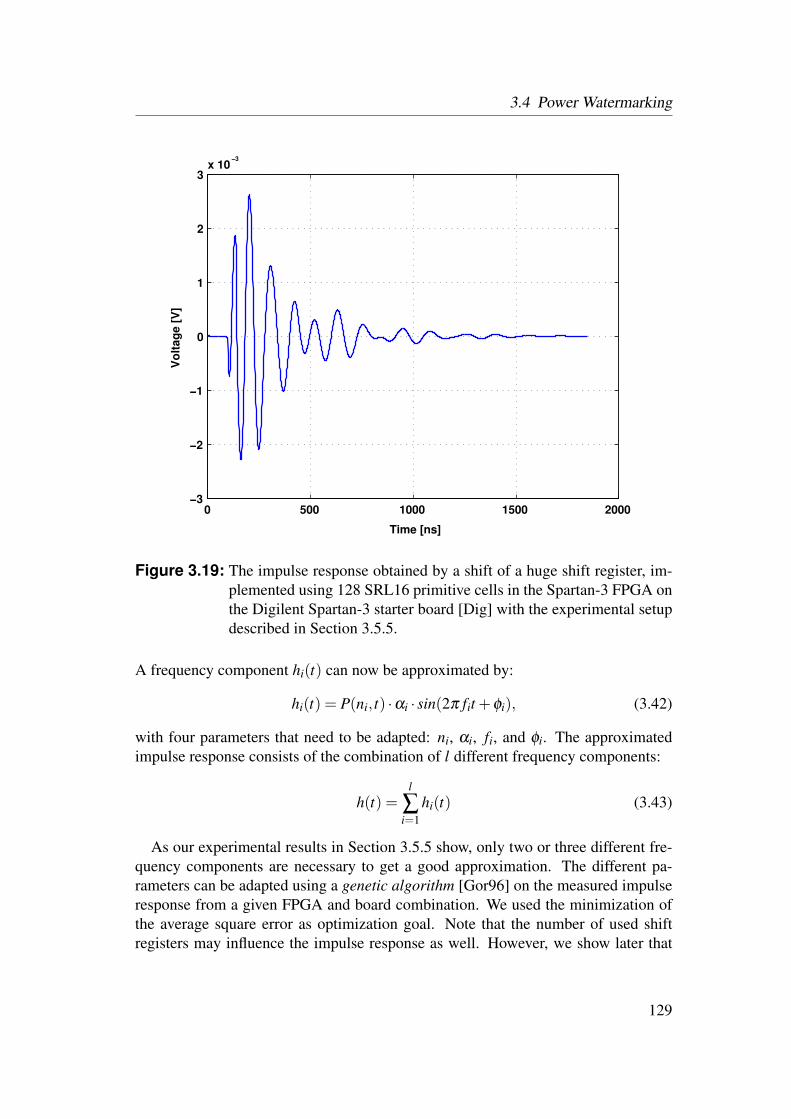
3.4 Power Watermarking
0 500 1000 1500 2000−3
−2
−1
0
1
2
3x 10
−3
Time [ns]
Vo
ltag
e [
V]
Figure 3.19: The impulse response obtained by a shift of a huge shift register, im-plemented using 128 SRL16 primitive cells in the Spartan-3 FPGA onthe Digilent Spartan-3 starter board [Dig] with the experimental setupdescribed in Section 3.5.5.
A frequency component hi(t) can now be approximated by:
hi(t) = P(ni, t) ·αi · sin(2π fit +φi), (3.42)
with four parameters that need to be adapted: ni, αi, fi, and φi. The approximatedimpulse response consists of the combination of l different frequency components:
h(t) =l
∑i=1
hi(t) (3.43)
As our experimental results in Section 3.5.5 show, only two or three different fre-quency components are necessary to get a good approximation. The different pa-rameters can be adapted using a genetic algorithm [Gor96] on the measured impulseresponse from a given FPGA and board combination. We used the minimization ofthe average square error as optimization goal. Note that the number of used shiftregisters may influence the impulse response as well. However, we show later that
129

3. IP Core Watermarking and Identification
the usage of more or less shift registers only influences the amplitude α of the signalwhich can be adapted by a constant factor.
Synchronization
For measuring the impulse response as well as for the decoding of the transmitteddata later, several repeated equal data sequences can be accumulated to reduce thenoise and disturbances which are not related to the sequence. For this approach, it isimportant that the individual sequences to be accumulated are exactly aligned overthe time axis. This can be done by synchronizing the oscilloscope sample clock withthe shift clock inside the FPGA.
Another way to get exact, noise-reduced data is by multiple oversampling insidethe oscilloscope for recording the measurements. Here, a subsequent resynchroniza-tion on the measured data might be necessary.
To check this, the different sequences are plotted on top of each other. If the se-quences match exactly, no resynchronization is necessary. If there is a shift over time,a resynchronization must be done. It is only necessary to look for the positions of themaxima if a sequence consists of only one event. A resynchronization is necessary ifthe positions of the maxima drift away over time and can be achieved by inserting orremoving samples for compensating the deviation.
Channel Approximation
The measured signal y(t) can be approximated with the help of the impulse response:
y(t) = c ·(∫ ∞−∞
h(τ) · x(t− τ)dτ
)+n(t). (3.44)
Here, x(t) is the input signal, consisting of Dirac-pulses which encode the signa-ture. For each Dirac-pulse, a scaled impulse response is inserted. The scaling factorc depends on the amplitude of the pulse which therefore corresponds to the numberof currently active shift registers. The assumption that the amplitude of the pulsesdepends linearly on the number of shift registers has been confirmed by experiment.Figure 3.20 shows the measured amplitude of the impulse response caused by differ-ent numbers of active shift registers.
Furthermore, the noise component n(t) has influence on the decoding quality. Thequality of the signal y(t) can be measured by the signal to noise ratio (SNR):.
SNR = c ·(∫ ∞−∞
h(τ) · x(t− τ)dτ
)· 1
n(t). (3.45)
If the SNR is low, it is difficult or impossible to correctly decode the correspondingsymbol. The SNR is therefore an indicator of how reliable the decoding of a givensignal is.
130
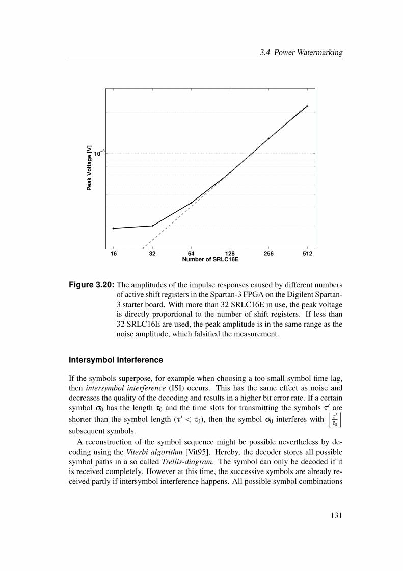
3.4 Power Watermarking
16 32 64 128 256 512
10−3
Number of SRLC16E
Peak V
olt
ag
e [
V]
Figure 3.20: The amplitudes of the impulse responses caused by different numbersof active shift registers in the Spartan-3 FPGA on the Digilent Spartan-3 starter board. With more than 32 SRLC16E in use, the peak voltageis directly proportional to the number of shift registers. If less than32 SRLC16E are used, the peak amplitude is in the same range as thenoise amplitude, which falsified the measurement.
Intersymbol Interference
If the symbols superpose, for example when choosing a too small symbol time-lag,then intersymbol interference (ISI) occurs. This has the same effect as noise anddecreases the quality of the decoding and results in a higher bit error rate. If a certainsymbol σ0 has the length τ0 and the time slots for transmitting the symbols τ ′ areshorter than the symbol length (τ ′ < τ0), then the symbol σ0 interferes with
⌊τ′
τ0
⌋subsequent symbols.
A reconstruction of the symbol sequence might be possible nevertheless by de-coding using the Viterbi algorithm [Vit95]. Hereby, the decoder stores all possiblesymbol paths in a so called Trellis-diagram. The symbol can only be decoded if itis received completely. However at this time, the successive symbols are already re-ceived partly if intersymbol interference happens. All possible symbol combinations
131
3. IP Core Watermarking and Identification
are stored in the Trellis-diagram, and if the decoder decides the value of the currentlycompletely received symbol, all combinations using the other values for the currentsymbol are deleted from the diagram.
3.4.3 Basic MethodIn this section, we describe the basic method for power watermarking of netlist cores.The concept, the embedding of the watermark, as well as the detection and verifica-tion procedure are described. The encoding and decoding for sending the signaturethrough the FPGA power communication channel is relatively simple and straight-forward in the basic method and will be refined later on with the enhanced methods.However, the basic concepts of embedding and the verification are very similar in allmethods.
For power watermarking, two shift registers are used, a large one for causing a rec-ognizable signature-dependent power consumption pattern, and a shift register stor-ing the signature itself (see Figure 3.15 in Section 3.4.1). The signature shift registeris clocked by the operational clock and the output bit enables the power pattern gen-erator. If the output bit is a ’1’, the power pattern register will be shifted at the nextrising edge of the operational clock. At a ’0’, no shift is done. Therefore, the channelencoding is Z = (γ,1,1),(γ,1,1). To avoid interference from the operational logicin the measured voltage, the signature is only generated during the reset phase of thecore.
As mentioned before in Section 3.3.5, a shift register can also be used as a lookuptable and vice versa in many FPGA architectures (see Figure 3.12 in Section 3.3.5).A conversion of functional lookup tables into shift registers does not affect the func-tionality if the new inputs are set correctly. This allows us to use functional logicfor implementing the power pattern generator. The core operates in two modes, thefunctional mode and the reset mode. In the functional mode, the shift is disabled andthe shift register operates as a normal lookup table. In the reset mode, the content isshifted according to the signature bits and consumes power which can be measuredoutside of the FPGA. To prevent the loss of the content of the lookup table, the outputof the shift register is fed back to the input, so the content is shifted circularly. Whenthe core changes to the functional mode, the content must be shifted to the properposition to have a functional lookup table for the core.
The amplitude of the generated power signature depends on the number and con-tent of the converted lookup tables. It will be assumed that the transitions betweenzeros and ones in the bit pattern of the lookup table contents are sufficient to pro-duce a recognizable pattern on the supply voltage. Experimental results in [Bau08]show that, on average, 8 of maximal 16 transitions are generated in functional 4 inputlookup tables of example cores if the content will be shifted.
To increase the robustness against removal and ambiguity attacks, the content ofthe power consumption shift register which is also part of the functional logic can be
132
3.4 Power Watermarking
initialized shifted. Only during the reset state, when the signature is transmitted, thecontent of the functional lookup table can be positioned correctly. So, normal coreoperation cannot start before the signature was transmitted completely. The advan-tage is that the core is only able to work after sending the signature. Furthermore, toavoid a too short reset time in which the watermark cannot be detected exactly, theright functionality will only be established if the reset state is longer than a predefinedtime. This prevents the user from leaving out or shorten the reset state with the resultthat the signature cannot be detected properly.
The signature itself can be implemented as a part of the functional logic in the sameway. Some lookup tables are connected together and the content, the function of theLUTs, represents the signature. Furthermore, techniques described in Section 3.3.5can be used to combine an additional watermark and the functional part in a singlelookup table if not all lookup table inputs are used for the function. For example,LUT2 primitives in Xilinx Virtex-II devices can be used to carry an additional 12-bit watermark by restricting the reachability of the functional lookup table throughclamping certain signals to constant values. Therefore, the final sending sequenceconsists of the functional part and the additional watermark. This principle makes italmost impossible for an attacker to change the content of the signature shift register.Altering the signature would also affect the functional core and thus result in a corruptcore.
The advantages of using the functional logic of the core also as a shift register area reduced resource overhead for watermarking and the robustness of this method, be-cause these shift registers are embedded in the functional design and it is hard, if notimpossible, to remove the shift registers without destroying the functionality of thecore. Furthermore, our watermarking procedure is difficult to be detected in a netlistfile, because the main part of the required logic for signature creation depends on thefunctional logic for the proper core. Another benefit is that our watermark cannotbe removed by an optimization step during the mapping into CLBs (ConfigurableLogic Blocks). Nevertheless, if an attacker had special knowledge of the watermark-ing method and of the EDIF netlist format, he may reverse-engineer the alterationof the embedding algorithm and remove or disable the sending method. This canbe avoided by initializing the power pattern register with shifted lookup table con-tents (see above). If sending of the signature is prevented, the core will not functionproperly.
Embedding of the Watermark
In this section, we describe the procedure of watermarking a core. The first step isto generate the watermark WL for embedding at the logic abstraction layer L. Asdescribed in the last section, the watermark is a bit sequence, consisting either of ran-dom choice bits, of partly functional bits of lookup tables, or completely of functionalbits. The watermark generation procedure depends on the sequence type.
133

3. IP Core Watermarking and Identification
If only random choice bits are used, the watermark generated needs only the uniquekey K which identifies the author of the core: GL(K) = WL. The unique key K canbe processed as depicted in Figure 3.4 in Section 3.2.2. The pseudo random outputcan be split into different shift registers: WL = wL1,wL2, . . . ,wLm. The numberof used shift registers m depends on the strength of the generated signature and theFPGA architecture. For example, a 128-bit signature can be stored in the Virtex-IIarchitecture in m = 8 shift registers.
If the content of functional lookup tables should be used as signature, the first stepis to extract all lookup tables form the netlist core: LL(IL) = lutL1 , lutL2, . . . , lutLr.The watermark generator GL searches for suitable functional lookup tables, trans-forms these into shift registers and either adds the watermark bits form the pseudorandom sequence GL(K,LL(IL)) = WL, or only uses the lookup table content as sig-nature: GL(LL(IL)) = WL.
The watermark embedder EL(IL,WL) = IL consists of two steps. First, the core ILmust be embedded in a wrapper which contains the control logic for emitting thesignature. This step is done at the register-transfer level before synthesis. The secondstep is at the logic level after the synthesis. A program converts suitable lookup tables(for example LUT4 for Virtex-II FPGAs) into shift registers for the generation of thepower pattern and attaches the corresponding control signal from the control logic inthe wrapper (see Figure 3.21).
The wrapper contains the control logic for emitting the watermark and the shiftregister, holding the signature. If functional lookup tables are used for implementingthe signature shift register, we add or convert this shift register in the second stepso that the wrapper contains only the control logic. Some control signals have nosink yet, because the sink will be added in the second step (e.g., the power patterngenerator shift register). So we must use synthesis constraints to prevent the synthesistool from optimizing these signals away. The ports of the wrapper are the same forthe core, so we can easily integrate this wrapper into the hierarchy. The controllogic shifts the signature shift register, while the core is in reset state. Also, thepower pattern shift register is shifted corresponding to the output of the signatureshift register. If the reset input of the wrapper gets inactive, the function of the corecannot start at the same cycle, because the positions of the content in the shift registerare not in the correct state. The control logic shifts the register content into the correctposition and leaves the reset state to start the normal operation mode.
The translation of lookup tables of the functional logic into shift registers is doneat the logic level. At Xilinx Virtex-II FPGAs, the usage of a LUT4 as a 16-bit shiftregister (SRL16) is only possible if the LUT4 is not part of a multiplexer logic, be-cause the additional shift logic and the multiplexer share common resources in a slice.Also, if the lookup table is a part of an adder, the mapping tool splits the lookup tableand the carry chain. In these two cases, additional slices would be required, so we donot convert these lookup tables into shift registers.
134

3.4 Power Watermarking
IP Core
Wrapper
Inputs
OutputsWM-
Control
Reset Reset
Signature
wmne LUT4
LUT4
Wrapper
Inputs
OutputsWM-
Control
Reset Reset
Signature
wmne SRL16
SRL16
Signature
IP Core
Figure 3.21: The core and the wrapper before (above) and after (below) the netlistalternation step. The signal “wmne” is an enable signal for shiftingthe power pattern generator shift register.
The embedding procedure for Virtex-II netlist cores is done by a program whichparses an EDIF netlist and writes back the modified EDIF netlist. First, the programreads all LUT4 instances and only select those that are not a “MUXF5”, a “MUXCY”or an “XORCY”. Then, the instances are converted to a shift register (SRL16), if re-quired, initialized with the shifted value and connected to the clock and the watermarkenable (wmne) signal according to Figure 3.21. Always two shift registers are con-nected together to rotate their contents. Finally, the modified netlist is created. Thewatermarked core IL is now ready for purchase or publication.
Detection Algorithm
A company may obtain an unlicensed version of the core IL and embeds this core in aproduct: IP = TL→B(IL I′L1
I′L2 . . .). If the core developer has a suspicious fact, he
135

3. IP Core Watermarking and Identification
can buy the product and verify that his signature is inside the core using a detectionfunction DP(IP,WL) = true/ f alse.
Detecting the basic power watermark, the measured voltage will be probed, digi-tized and decoded by a signature detection algorithm (see Figure 3.22). To decodethe digitalized voltage signal, the sampling rate, the clock frequency of the shiftedsignature and the bit length of the signature is needed. The clock frequency can beextracted using the Fast Fourier Transformation (FFT) of the measured signal. Ourdetection algorithm consists of five steps: down sampling, differential step, accu-mulation step, phase detection and quantization (see Figure 3.22). After successfulextraction, the decoded signature can be compared to the signature inside the water-mark WL to establish the ownership. Furthermore, the signature must be verified bycryptographic methods with the author’s unique key K. The key verification proce-dure is very similar to the bitfile watermarking methods presented in Section 3.3.
downsamplingclk freq.
sample freq.
probed voltage signal Spr
differential stepxdt
accumulation step∑ x
phase detection
quantization
decoded signature
SDS
SD
SAS
Figure 3.22: The five steps of the watermark detection algorithm: downsampling,differential and accumulation step, phase detection and finally quanti-zation.
As mentioned before, the main characteristic caused by a switching event is thedrop of the voltage followed by a subsequent overshoot. This results in extremeslopes. The basic method detection algorithm can find each rising edge as follows:First, the measured signal will be sampled down from the recorded sample rate to the
136

3.4 Power Watermarking
quadruple of the clock frequency, so each signature bit is represented by four samples.Then, the discrete derivative of the signal will be calculated. This transforms therising edges of the switching events into peaks. The easiest way to calculate thediscrete derivative at a discrete point in time SD[k] is to take the difference of twosubsequent samples over time (see Figure 3.23).
SD[k] = SDS[k]−SDS[k−1], (3.46)
where SDS is the down sampled probed voltage signal and k denotes the sample index.
0 2 4 6 8 10 12 14 16−4
−2
0
2
k
SD
S[k
]
0 2 4 6 8 10 12 14 16−4
−2
0
2
4
6
k
SD[k
]
Figure 3.23: An example voltage signal which represents the signature “0011”(above). The example voltage signal after the differentiation step (be-low).
Since the signature is repeated many times during the reset state, the signal canbe accumulated and averaged to reduce the noise level. To accumulate the coherentpattern, we need to know the bit length of the signature. If we record a longer signalsequence, we can accumulate more patterns and reduce noise as well as switchingevents which do not belong to the power consumption register of the watermarkingalgorithm. The disadvantage is that we would need a longer time for the reset phase.
After this third step, we have a signal in which each signature bit is represented byfour samples. But only one sample carries the information of the rising edge. Since
137
3. IP Core Watermarking and Identification
the measurement is not synchronized with the FPGA clock, the phase (position) ofthe relevant sample of a bit is unknown. We divide the signal into four new signals,where one signature bit is represented in one sample. The four signals have a phaseshift of 90o to each other. Let
SAS[k], k = 0,1, ..,4m−1 (3.47)
denote the sampled voltage signal after the accumulation step where m is the lengthof the signature. Then, we obtain the four following phase shifted signals
S0 = SAS[4k], k = 0,1, ..,m−1 (3.48)S90 = SAS[4k +1], ” (3.49)
S180 = SAS[4k +2], ” (3.50)S270 = SAS[4k +3], ” (3.51)
where SAS is the accumulated signal and S0, S90, S180, and S270 are the phase signals(see Figure 3.24).
We are able to extract the right phase of the signal if we calculate the mean value ofeach phase-shifted signal. The maximal mean value corresponds to the correct phase,because the switching event should cause the greatest rising edge in the signal.
Now, we have a signal in which each sample is represented by the accumulatedswitching activities of one bit of the signature. The decision if the sample correspondsto a signature bit ’1’ or ’0’ can be done by comparing the sample value with the meanvalue of the signal. If the sample value is higher than the mean value, the algorithmdecides a ’1’, in the other case a ’0’.
Robustness Analysis
The most common attacks against watermarking mentioned in Section 3.2.1 are re-moval, ambiguity, key copy, and copy attacks. Once again, key copy attacks can beprevented by asymmetric cryptographic methods, and there is no protection againstcopy attacks.
Removal attacks most likely take place on the logic level instead of the device levelwhere it is really hard to alter the design. The signature and power shift registers aswell as the watermark sending control logic in the wrapper are mixed with functionalelements in the netlist. Therefore, they are not easy to detect. Even if an attackeris able to identify the sending logic, a deactivation is useless if the content of thepower shift register is only shifted into correct positions after sending the signature.By preventing the sending of the watermark, the core is unable to start. Anotherpossibility is to alter the signature inside the shift register. The attacker may analyzethe netlist to find the place were the signature is stored. This attack is only successful
138
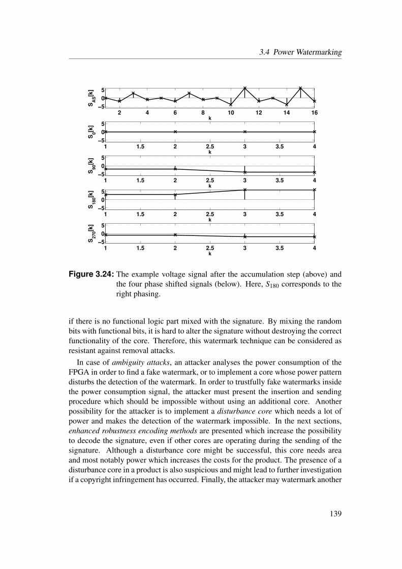
3.4 Power Watermarking
2 4 6 8 10 12 14 16−5
0
5
k
SA
S[k
]
1 1.5 2 2.5 3 3.5 4−5
0
5
k
S0[k
]
1 1.5 2 2.5 3 3.5 4−5
0
5
k
S90[k
]
1 1.5 2 2.5 3 3.5 4−5
0
5
k
S180[k
]
1 1.5 2 2.5 3 3.5 4−5
0
5
k
S270[k
]
Figure 3.24: The example voltage signal after the accumulation step (above) andthe four phase shifted signals (below). Here, S180 corresponds to theright phasing.
if there is no functional logic part mixed with the signature. By mixing the randombits with functional bits, it is hard to alter the signature without destroying the correctfunctionality of the core. Therefore, this watermark technique can be considered asresistant against removal attacks.
In case of ambiguity attacks, an attacker analyses the power consumption of theFPGA in order to find a fake watermark, or to implement a core whose power patterndisturbs the detection of the watermark. In order to trustfully fake watermarks insidethe power consumption signal, the attacker must present the insertion and sendingprocedure which should be impossible without using an additional core. Anotherpossibility for the attacker is to implement a disturbance core which needs a lot ofpower and makes the detection of the watermark impossible. In the next sections,enhanced robustness encoding methods are presented which increase the possibilityto decode the signature, even if other cores are operating during the sending of thesignature. Although a disturbance core might be successful, this core needs areaand most notably power which increases the costs for the product. The presence of adisturbance core in a product is also suspicious and might lead to further investigationif a copyright infringement has occurred. Finally, the attacker may watermark another
139
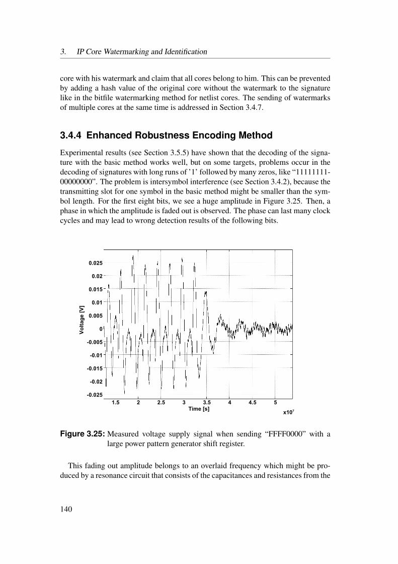
3. IP Core Watermarking and Identification
core with his watermark and claim that all cores belong to him. This can be preventedby adding a hash value of the original core without the watermark to the signaturelike in the bitfile watermarking method for netlist cores. The sending of watermarksof multiple cores at the same time is addressed in Section 3.4.7.
3.4.4 Enhanced Robustness Encoding Method
Experimental results (see Section 3.5.5) have shown that the decoding of the signa-ture with the basic method works well, but on some targets, problems occur in thedecoding of signatures with long runs of ’1’ followed by many zeros, like “11111111-00000000”. The problem is intersymbol interference (see Section 3.4.2), because thetransmitting slot for one symbol in the basic method might be smaller than the sym-bol length. For the first eight bits, we see a huge amplitude in Figure 3.25. Then, aphase in which the amplitude is faded out is observed. The phase can last many clockcycles and may lead to wrong detection results of the following bits.
4 4.5 52.5 3.51.5 2 3Time [s]
x107
0.005
0
-0.005
0.01
0.015
0.02
0.025
-0.01
-0.015
-0.02
-0.025
Vo
ltag
e [V
]
Figure 3.25: Measured voltage supply signal when sending “FFFF0000” with alarge power pattern generator shift register.
This fading out amplitude belongs to an overlaid frequency which might be pro-duced by a resonance circuit that consists of the capacitances and resistances from the
140

3.4 Power Watermarking
power supply plane and its blocking capacitances (see Section 3.4.2). This behavioris dependent on the printed circuit board and the power supply circuit.
To avoid such a false detection, the transmission time of one symbol is extended bythe time of the swing out of the printed circuit board by sending the same signaturebit multiple times: Z = (γ,1,ω),(γ,1,ω). The repetition rate for each signaturebit is ω clock cycles. If we connect two SRL16 together, one period for this shiftregister needs 32 clock cycles. If the reset phase ends and we have finished sendingone bit, the content in the shift register which also represents a part of the logic of thecore is in the correct position.
The detection algorithm differs for this method. First, the signal will be sampleddown and the approximate derivation will be calculated as in the original method (seeSection 3.4.3). Now, we average the signal to suppress the noise. Here, the lengthof one signature word is the length of the signature (m) multiplied by the number oftimes each bit is sent (ω).
SD[k], k = 0,1, ..,Kmax−1 (3.52)
ns =⌊ Kmax
4ω ·m⌋, (3.53)
S =1ns
ns−1
∑i=0
D[4ω ·m · i, ..,4ω ·n · i+4ω ·m−1], (3.54)
Here, SD is the voltage signal after the differential step with index k and ns being thenumber of repetitions of the pattern in SD.
The phase detection of the shift clock is the same as in the original method (seeSection 3.4.3), but we also need the position p where a new signature bit starts. Thisis done in a loop to detect this position. In the beginning, we assume that the startingposition is the beginning of our trace (p = 0). First, we accumulate ω successivevalues where ω is the repetition of one bit:
Sp[ j] =ω−1
∑i=0
Sφ [i+ p+ω j], j = 0,1, ..,m−1 (3.55)
Here, Sφ denotes the signal after the phase detection step. Now, we subtract the meanvalue and generate the absolute value and calculate the sum of it.
Fp =n−1
∑i=0
∣∣∣Sp[i]− 1n
n−1
∑j=0
Sp[ j]∣∣∣ (3.56)
Fp identifies how good our signature bit starting position p fits the real position.Now, we shift our trace one value (p = 1) and calculate the fitting value again, and
141
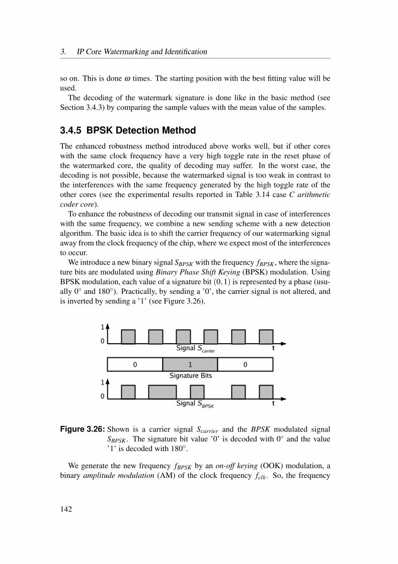
3. IP Core Watermarking and Identification
so on. This is done ω times. The starting position with the best fitting value will beused.
The decoding of the watermark signature is done like in the basic method (seeSection 3.4.3) by comparing the sample values with the mean value of the samples.
3.4.5 BPSK Detection MethodThe enhanced robustness method introduced above works well, but if other coreswith the same clock frequency have a very high toggle rate in the reset phase ofthe watermarked core, the quality of decoding may suffer. In the worst case, thedecoding is not possible, because the watermarked signal is too weak in contrast tothe interferences with the same frequency generated by the high toggle rate of theother cores (see the experimental results reported in Table 3.14 case C arithmeticcoder core).
To enhance the robustness of decoding our transmit signal in case of interferenceswith the same frequency, we combine a new sending scheme with a new detectionalgorithm. The basic idea is to shift the carrier frequency of our watermarking signalaway from the clock frequency of the chip, where we expect most of the interferencesto occur.
We introduce a new binary signal SBPSK with the frequency fBPSK , where the signa-ture bits are modulated using Binary Phase Shift Keying (BPSK) modulation. UsingBPSK modulation, each value of a signature bit (0,1) is represented by a phase (usu-ally 0 and 180). Practically, by sending a ’0’, the carrier signal is not altered, andis inverted by sending a ’1’ (see Figure 3.26).
0
t
1 0
t0
1
Signature Bits
tt0
1
Signal SBPSK
Signal Scarrier
Figure 3.26: Shown is a carrier signal Scarrier and the BPSK modulated signalSBPSK . The signature bit value ’0’ is decoded with 0 and the value’1’ is decoded with 180.
We generate the new frequency fBPSK by an on-off keying (OOK) modulation, abinary amplitude modulation (AM) of the clock frequency fclk. So, the frequency
142
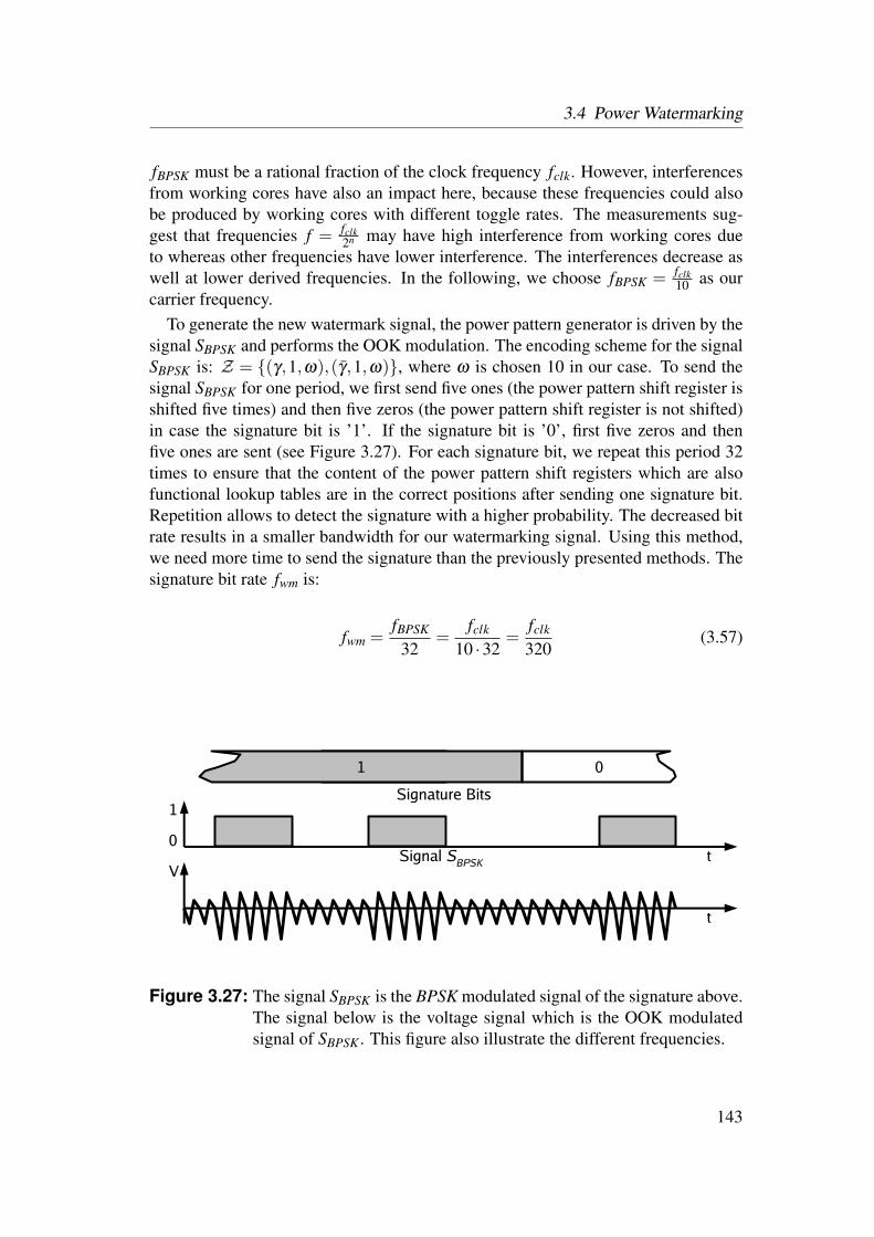
3.4 Power Watermarking
fBPSK must be a rational fraction of the clock frequency fclk. However, interferencesfrom working cores have also an impact here, because these frequencies could alsobe produced by working cores with different toggle rates. The measurements sug-gest that frequencies f = fclk
2n may have high interference from working cores dueto whereas other frequencies have lower interference. The interferences decrease aswell at lower derived frequencies. In the following, we choose fBPSK = fclk
10 as ourcarrier frequency.
To generate the new watermark signal, the power pattern generator is driven by thesignal SBPSK and performs the OOK modulation. The encoding scheme for the signalSBPSK is: Z = (γ,1,ω),(γ,1,ω), where ω is chosen 10 in our case. To send thesignal SBPSK for one period, we first send five ones (the power pattern shift register isshifted five times) and then five zeros (the power pattern shift register is not shifted)in case the signature bit is ’1’. If the signature bit is ’0’, first five zeros and thenfive ones are sent (see Figure 3.27). For each signature bit, we repeat this period 32times to ensure that the content of the power pattern shift registers which are alsofunctional lookup tables are in the correct positions after sending one signature bit.Repetition allows to detect the signature with a higher probability. The decreased bitrate results in a smaller bandwidth for our watermarking signal. Using this method,we need more time to send the signature than the previously presented methods. Thesignature bit rate fwm is:
fwm =fBPSK
32=
fclk
10 ·32=
fclk
320(3.57)
1
t0
1Signature Bits
t
VSignal SBPSK
1 0
Figure 3.27: The signal SBPSK is the BPSK modulated signal of the signature above.The signal below is the voltage signal which is the OOK modulatedsignal of SBPSK . This figure also illustrate the different frequencies.
143
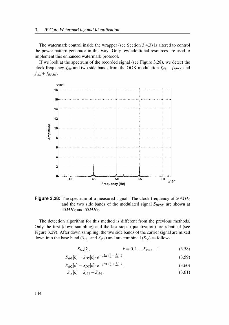
3. IP Core Watermarking and Identification
The watermark control inside the wrapper (see Section 3.4.3) is altered to controlthe power pattern generator in this way. Only few additional resources are used toimplement this enhanced watermark protocol.
If we look at the spectrum of the recorded signal (see Figure 3.28), we detect theclock frequency fclk and two side bands from the OOK modulation fclk− fBPSK andfclk + fBPSK .
45 1500
40 50
Frequency [Hz]x106
2
60
4
6
8
10
12
14
16
Am
pli
tud
e
55
18
x10-4
Figure 3.28: The spectrum of a measured signal. The clock frequency of 50MHzand the two side bands of the modulated signal SBPSK are shown at45MHz and 55MHz.
The detection algorithm for this method is different from the previous methods.Only the first (down sampling) and the last steps (quantization) are identical (seeFigure 3.29). After down sampling, the two side bands of the carrier signal are mixeddown into the base band (Ssb1 and Ssb2) and are combined (Scc) as follows:
SDS[k], k = 0,1, ..,Kmax−1 (3.58)
Ssb1[k] = SDS[k] · e− j2π·( 14−
140 )·k, (3.59)
Ssb2[k] = SDS[k] · e− j2π·( 14 + 1
40 )·k, (3.60)Scc[k] = Ssb1 +Ssb2, (3.61)
144
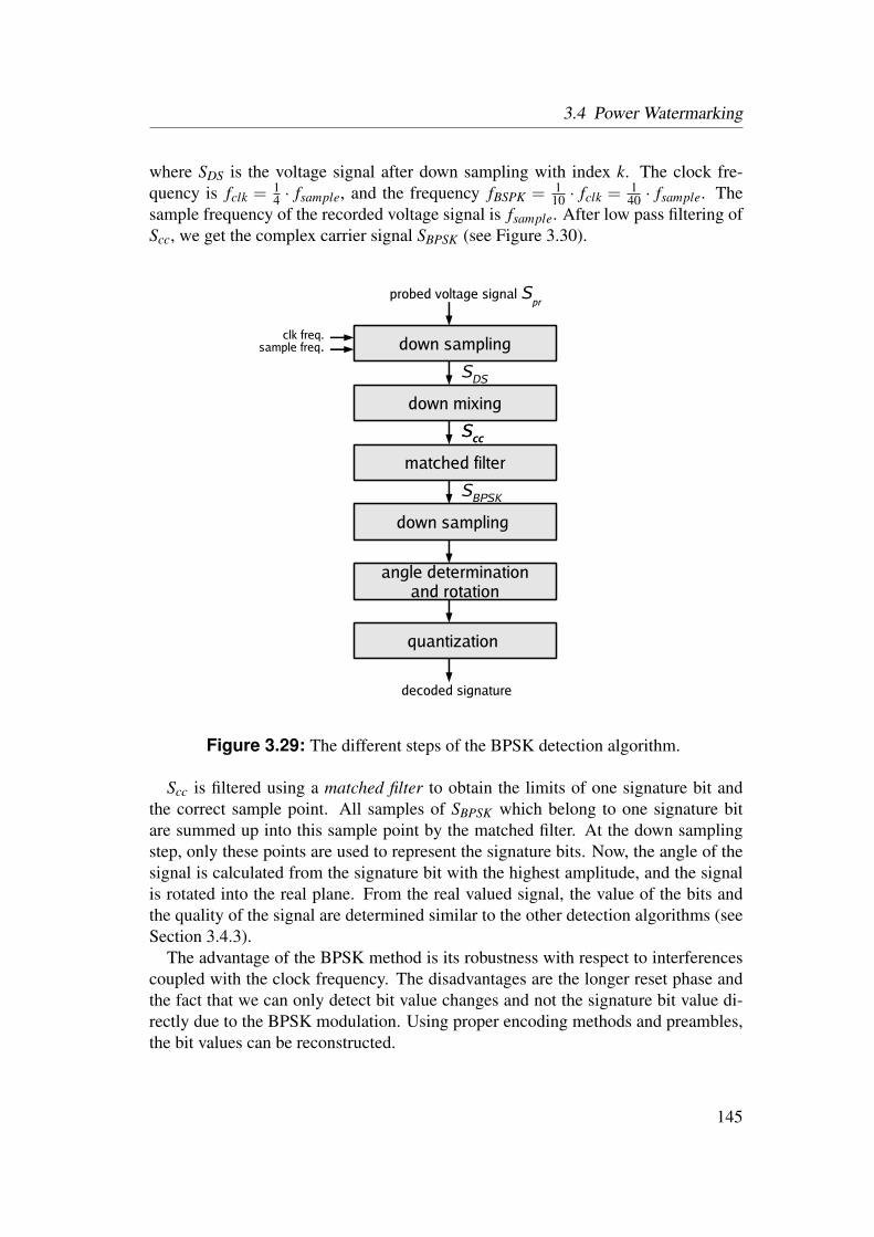
3.4 Power Watermarking
where SDS is the voltage signal after down sampling with index k. The clock fre-quency is fclk = 1
4 · fsample, and the frequency fBSPK = 110 · fclk = 1
40 · fsample. Thesample frequency of the recorded voltage signal is fsample. After low pass filtering ofScc, we get the complex carrier signal SBPSK (see Figure 3.30).
down samplingclk freq.
sample freq.
probed voltage signal Spr
down mixing
down sampling
angle determinationand rotation
quantization
decoded signature
matched filter
SccScc
SDS
SBPSK
Figure 3.29: The different steps of the BPSK detection algorithm.
Scc is filtered using a matched filter to obtain the limits of one signature bit andthe correct sample point. All samples of SBPSK which belong to one signature bitare summed up into this sample point by the matched filter. At the down samplingstep, only these points are used to represent the signature bits. Now, the angle of thesignal is calculated from the signature bit with the highest amplitude, and the signalis rotated into the real plane. From the real valued signal, the value of the bits andthe quality of the signal are determined similar to the other detection algorithms (seeSection 3.4.3).
The advantage of the BPSK method is its robustness with respect to interferencescoupled with the clock frequency. The disadvantages are the longer reset phase andthe fact that we can only detect bit value changes and not the signature bit value di-rectly due to the BPSK modulation. Using proper encoding methods and preambles,the bit values can be reconstructed.
145
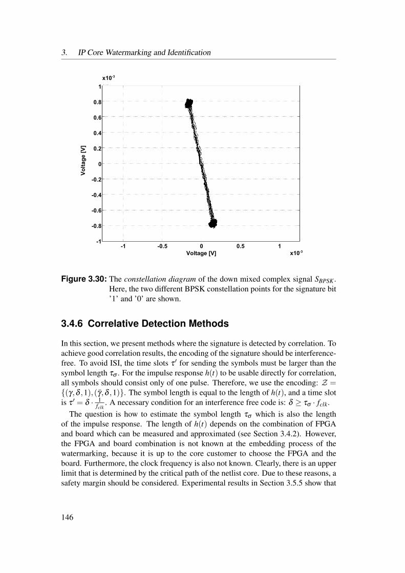
3. IP Core Watermarking and Identification
0.5 1-0.5 0-1Voltage [V] x10-3
0.2
0
-0.2
0.4
0.6
0.8
-0.4
-0.6
-0.8
-1
Vo
lta
ge
[V
]x10-3
1
Figure 3.30: The constellation diagram of the down mixed complex signal SBPSK .Here, the two different BPSK constellation points for the signature bit’1’ and ’0’ are shown.
3.4.6 Correlative Detection Methods
In this section, we present methods where the signature is detected by correlation. Toachieve good correlation results, the encoding of the signature should be interference-free. To avoid ISI, the time slots τ ′ for sending the symbols must be larger than thesymbol length τσ . For the impulse response h(t) to be usable directly for correlation,all symbols should consist only of one pulse. Therefore, we use the encoding: Z =(γ,δ ,1),(γ,δ ,1). The symbol length is equal to the length of h(t), and a time slotis τ ′ = δ · 1
fclk. A necessary condition for an interference free code is: δ ≥ τσ · fclk.
The question is how to estimate the symbol length τσ which is also the lengthof the impulse response. The length of h(t) depends on the combination of FPGAand board which can be measured and approximated (see Section 3.4.2). However,the FPGA and board combination is not known at the embedding process of thewatermarking, because it is up to the core customer to choose the FPGA and theboard. Furthermore, the clock frequency is also not known. Clearly, there is an upperlimit that is determined by the critical path of the netlist core. Due to these reasons, asafety margin should be considered. Experimental results in Section 3.5.5 show that
146

3.4 Power Watermarking
between 80 and 100 ns after the start of the symbol, 90% of the energy is emitted andafter 125 ns, over 95%. If we assume clock frequencies fclk < 200 MHz, then thenumber of clock cycles δ = 25 used for sending one symbol should be sufficient.
In this method, the detection of the signature is done by correlation. The cross-correlation Zx,y(t) of two function x(t),y(t) is defined as:
Zx,y(t) =∫ ∞−∞
x∗(t) · y(t + τ)dτ. (3.62)
In Equation 3.62, x∗(t) denotes to the complex conjugate of x(t). The cross-correlation is a measure of the similarity of the functions x(t) and y(t), if y(t) isshifted over the time axis t. The maximum of Zx,y(t) denotes the time with the high-est similarity.
To detect a signature, we can use two different correlation methods. In the firstmethod, the existence of a certain signature should be proven. From the adoptedsequence, the expected signal is constructed by inserting the approximated impulseresponse h(t) at times where the signature bit ’1’ should be sent, corresponding tothe encoding scheme: Z = (γ,δ ,1),(γ,δ ,1). The constructed signal is cross-correlated with the measured signal. If the maximum of cross-correlation is a dis-tinctive peak, a watermarked core with this signature may be present. The disadvan-tage of this method is to define the notion of a distinctive peak. If the signature isnot present in the core or another signature is present, the cross-correlation has alsopeaks (see Figure 3.31). It is hard to decide if the maximum peak belongs to thecorrect signature or not. Furthermore, if the expected and the actual present signatureare very similar and differ only in a few bits, the maximum of the cross-correlationis also a distinctive peak which is only a little bit lower than the peak of the correctsignature. Due to this problem, this approach does not seem to be applicable.
The second detection approach correlates the signal with the approximated impulseresponse h(t). If the signature bit ’1’ was sent, then the correlation result has a peak atthis position, otherwise, when a ’0’ was sent, no peak occurs. For better decoding, thesignal and the impulse response are mixed down into the base band of one frequencycomponent of h(t), e.g., h1(t). Then, the mixed down signal and impulse responseare correlated. Figure 3.32 shows such a correlation result. A possible decodingalgorithm can look at the positions of the symbols in order to find peaks. If the firstsymbol position is known, the other positions can be calculated based on the encodingscheme and the clock frequency. The symbols on these positions can be decoded bymaking a threshold decision. If the signal value is higher than a certain threshold,the decoder decides on a ’1’, otherwise on a ’0’. However, measurements showsthat after transmission of several bits with the value ’1’, the absolute peak values areincreasing slowly (see Figure 3.32). Therefore, the threshold value must be adapteddynamically based on the precedented values.
147
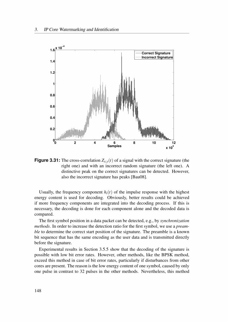
3. IP Core Watermarking and Identification
0 2 4 6 8 10 12
x 104
0
0.2
0.4
0.6
0.8
1
1.2
1.4
1.6x 10
−4
Samples
Correct Signature
Incorrect Signature
Figure 3.31: The cross-correlation Zx,y(t) of a signal with the correct signature (theright one) and with an incorrect random signature (the left one). Adistinctive peak on the correct signatures can be detected. However,also the incorrect signature has peaks [Bau08].
Usually, the frequency component hi(t) of the impulse response with the highestenergy content is used for decoding. Obviously, better results could be achievedif more frequency components are integrated into the decoding process. If this isnecessary, the decoding is done for each component alone and the decoded data iscompared.
The first symbol position in a data packet can be detected, e.g., by synchronizationmethods. In order to increase the detection ratio for the first symbol, we use a pream-ble to determine the correct start position of the signature. The preamble is a knownbit sequence that has the same encoding as the user data and is transmitted directlybefore the signature.
Experimental results in Section 3.5.5 show that the decoding of the signature ispossible with low bit error rates. However, other methods, like the BPSK method,exceed this method in case of bit error rates, particularly if disturbances from othercores are present. The reason is the low energy content of one symbol, caused by onlyone pulse in contrast to 32 pulses in the other methods. Nevertheless, this method
148
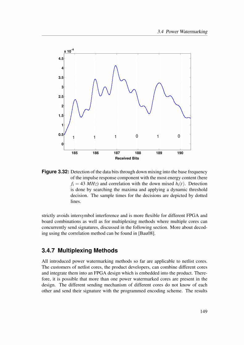
3.4 Power Watermarking
185 186 187 188 189 190
0
0.5
1
1.5
2
2.5
3
3.5
4
4.5
x 10−6
Received Bits
1 1 1 0 1 0
Figure 3.32: Detection of the data bits through down mixing into the base frequencyof the impulse response component with the most energy content (herefi = 43 MHz) and correlation with the down mixed hi(t). Detectionis done by searching the maxima and applying a dynamic thresholddecision. The sample times for the decisions are depicted by dottedlines.
strictly avoids intersymbol interference and is more flexible for different FPGA andboard combinations as well as for multiplexing methods where multiple cores canconcurrently send signatures, discussed in the following section. More about decod-ing using the correlation method can be found in [Bau08].
3.4.7 Multiplexing Methods
All introduced power watermarking methods so far are applicable to netlist cores.The customers of netlist cores, the product developers, can combine different coresand integrate them into an FPGA design which is embedded into the product. There-fore, it is possible that more than one power watermarked cores are present in thedesign. The different sending mechanism of different cores do not know of eachother and send their signature with the programmed encoding scheme. The results
149
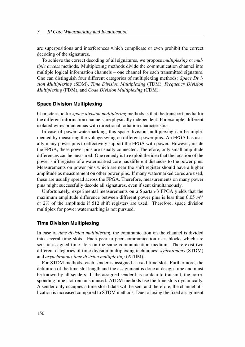
3. IP Core Watermarking and Identification
are superpositions and interferences which complicate or even prohibit the correctdecoding of the signatures.
To achieve the correct decoding of all signatures, we propose multiplexing or mul-tiple access methods. Multiplexing methods divide the communication channel intomultiple logical information channels – one channel for each transmitted signature.One can distinguish four different categories of multiplexing methods: Space Divi-sion Multiplexing (SDM), Time Division Multiplexing (TDM), Frequency DivisionMultiplexing (FDM), and Code Division Multiplexing (CDM).
Space Division Multiplexing
Characteristic for space division multiplexing methods is that the transport media forthe different information channels are physically independent. For example, differentisolated wires or antennas with directional radiation characteristics.
In case of power watermarking, this space division multiplexing can be imple-mented by measuring the voltage swing on different power pins. An FPGA has usu-ally many power pins to effectively support the FPGA with power. However, insidethe FPGA, these power pins are usually connected. Therefore, only small amplitudedifferences can be measured. One remedy is to exploit the idea that the location of thepower shift register of a watermarked core has different distances to the power pins.Measurements on power pins which are near the shift register should have a higheramplitude as measurement on other power pins. If many watermarked cores are used,these are usually spread across the FPGA. Therefore, measurements on many powerpins might successfully decode all signatures, even if sent simultaneously.
Unfortunately, experimental measurements on a Spartan-3 FPGA yields that themaximum amplitude difference between different power pins is less than 0.05 mVor 2% of the amplitude if 512 shift registers are used. Therefore, space divisionmultiplex for power watermarking is not pursued.
Time Division Multiplexing
In case of time division multiplexing, the communication on the channel is dividedinto several time slots. Each peer to peer communication uses blocks which aresent in assigned time slots on the same communication medium. There exist twodifferent categories of time division multiplexing techniques: synchronous (STDM)and asynchronous time division multiplexing (ATDM).
For STDM methods, each sender is assigned a fixed time slot. Furthermore, thedefinition of the time slot length and the assignment is done at design-time and mustbe known by all senders. If the assigned sender has no data to transmit, the corre-sponding time slot remains unused. ATDM methods use the time slots dynamically.A sender only occupies a time slot if data will be sent and therefore, the channel uti-lization is increased compared to STDM methods. Due to losing the fixed assignment
150

3.4 Power Watermarking
of the slots, the demultiplexer must know the receiver of the data. This is usually doneby sending the receiver information over the channel, for example, in the header ofthe data. Therefore, these methods are also known as address multiplexing methods.The time slot length is either fixed or variable, depending on the used technique.
The problem of adapting the TDM approach for power watermarking is that thesenders, the different power watermarked cores, have no synchronization possibili-ties. The reset signal might be used for synchronization, however, the different coresmay use different resets or clocks and due to the power watermarking methods, thereset length might be further altered. Therefore, a probabilistic approach for timedivision multiplexing is chosen, where each signature is sent with a given period.During one period, the signature is sent once and after that, the power pattern gener-ator inside the watermarked core is inactive until the period ends. The period lengthφi consists of the time for sending the signature tsig,i and the waiting time twait,i:φi = tsig,i + twait,i. By choosing different waiting times twait,i for different cores, thesending time of the different signatures drifts away over the time and the probabilityof a successful decoding increases with a higher measurement time (see Figure 3.33).One constraint on this method is that every watermarked core has its own unique pe-riod length φi which should be relatively prime to the period length of the other coresin order to minimize the superposition of different signatures. If nmax is the overallnumber of all existing power watermarked cores, then
GCD(φi,φ j) = 1 ∀i, j ∈ 1, . . . ,nmax. (3.63)
If all cores begin the transmission at the same start time, then the time span tdec forthe first collision-free decoding for two cores is:
tdec = φi ·⌈
tsig,i
φ j−φi
⌉, if φi < φ j, (3.64)
and for three cores:
tdec = LCM(
φi ·⌈
tsig,i
φ j−φi
⌉,φi ·
⌈tsig,i
φk−φi
⌉,φ j ·
⌈tsig, j
φk−φ j
⌉), if φi < φ j < φk.
(3.65)
To estimate the period length for real systems, we must first know how long thetime tsig for sending the signature is. For the correlation method, the usual symbollength is 200 ns. If we assume a signature length of 32 bit plus 12-bit preamble, thetime for sending the signature is: tsig = 8.8 µs. Furthermore, we need some timeto shift the power shift register to the right position for the functional logic. For theenhanced robustness method, the time for sending is ω · n · f−1
clk . With n = ω = 32and fclk = 50 MHz, we need 20.48 µs for sending the signature. Therefore, a value
151
3. IP Core Watermarking and Identification
A
0 5 10 15 20 25 30 35 40 45 50
A A A A A
B
0 5 10 15 20 25 30 35 40 45 50
B B B B
C
0 5 10 15 20 25 30 35 40 45 50
0 5 10 15 20 25 30 35 40 45 50
B B
C C C C
C A B C A C A C A
t
t
t
t
Signature A
Signature B
Signature C
TDM Channel
Figure 3.33: A schematic example for the application of the TDM method withthe transmission of three different signatures of different lengths. Theused periods are very short: φA = 9,φB = 10, and φC = 11 slots. Thetime slots with collisions are marked on the TDM channel row below.The first collision-free sending of all signatures is after time step t =22.
of 40 µs is a good approximation. One exception is the BPSK method. The sendingtime of a 32-bit signature there is 205 µs with fc = fclk
10 and fclk = 50 MHz.On the other hand, the sending of the watermarks is limited by the minimal reset
time, because all our power watermarking methods send the signature in the resetphase. If we assume a reset time of trst = 100 ms, and we would like to send each sig-nature at least 20 times for reasons of better decoding, then the maximum repetitionperiod is φ0 = 5 ms. For each additional signature, we reduce the period length bythe approximated 40 µs for sending the signature: φ1 = 4.96 ms,φ2 = 4.92 ms, . . . .Using this scheme, we have enough period times for signatures and a realistic resettime. Figure 3.34 shows a measurement of sending three different signatures usingour TDM method.
Frequency Division Multiplexing
In case of frequency division multiplexing (FDM), the different information channelsare assigned to different carrier frequencies. This can be done by modulating theinformation on a certain frequency. Different modulation methods, like amplitude(AM), frequency (FM), or phase modulation (PM) can be used. Furthermore, digital
152

3.4 Power Watermarking
30
Signature A
1.5 2.50.5 1 2Time [s] x106
0.5
0
-0.5
1.5
2
2.5
-1
-1.5
-2
-2.5
Vo
lta
ge
[mV
]
1
Signature C Signature B
Figure 3.34: Shown is the superposed sending of three different signatures usingthe TDM method on a Spartan-3 FPGA. The minimal period differ-ence between the signatures is approximately 16 µs. Signature A isproduced by 64 SRL16 shift registers, signature B uses 40 SRL16 shiftregisters, and signature C uses 25 SRL16 shift registers. In the mea-surement, collisions and proper decodeable signature transmissionsare highlighted.
signals are often transmitted using shift keying modulation, for example FrequencyShift Keying (FSK) or Phase Shift Keying (PSK).
The BPSK method, introduced in Section 3.4.5 uses an on-off keying (OOK) mod-ulation to shift the carrier frequency for sending the signature away from the clockfrequency. The aim of this modulation was the improved decoding, because mostinterferences from other cores are on the clock frequency or its divisions. However,using different carrier frequencies, more than one core can simultaneously send itssignature. The information of the signature bits is embedded into the carrier signalSBPSK by a BPSK modulation. Each watermarked core has its own carrier signalSBPSK,i which is OOK-modulated onto the clock frequency with different encodingschemes: Z = (γ,1,ωi),(γ,1,ωi). By choosing different repetition rates ωi, thedifferent signals SBPSK,i are sent on different frequencies which enables a congruentsending of all signatures. However, the number of usable frequencies or repetitionrates ωi is constrained by the clock frequency and the sending time of the signature.Nevertheless, this is an interesting approach for further research.
Code Division Multiplexing
Finally for code division multiplexing methods, the transmitted data from differentsenders are spread up with different unique codes, so called chips. A chip is either
153
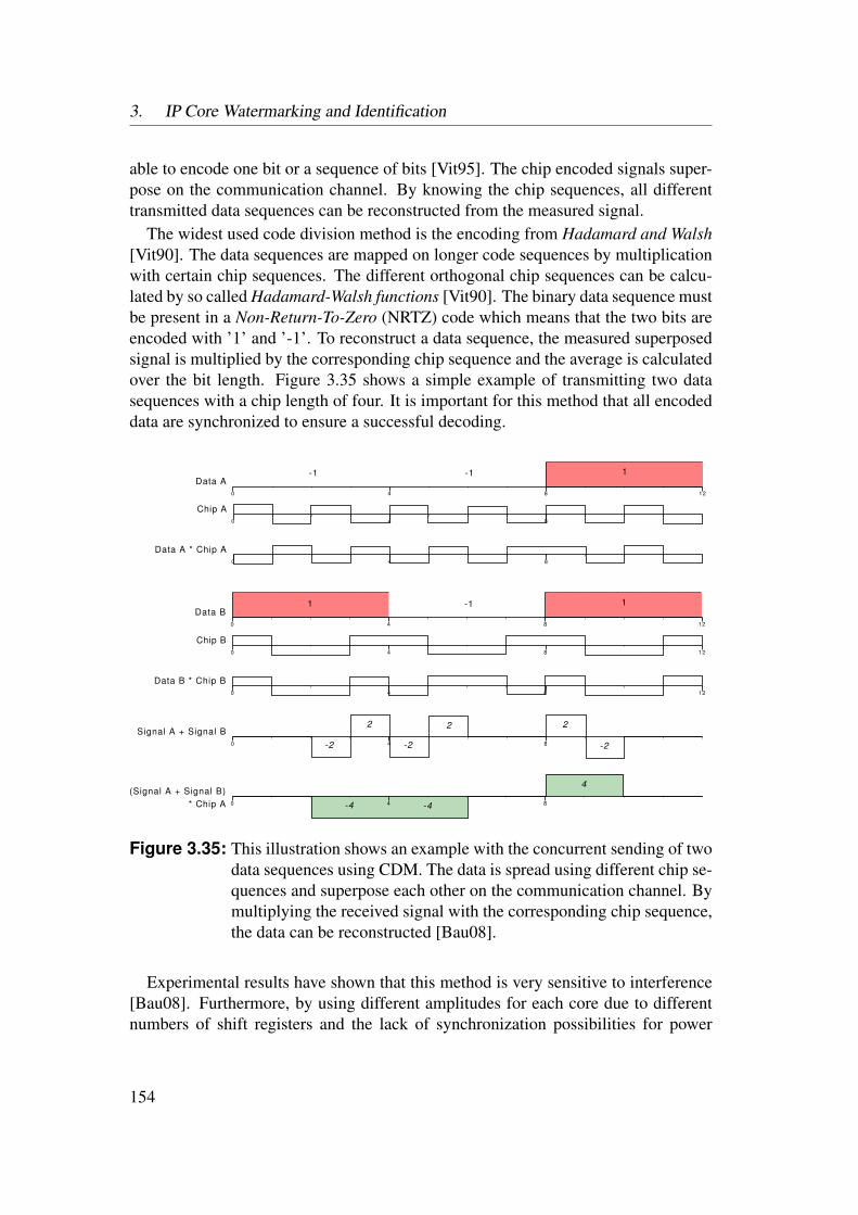
3. IP Core Watermarking and Identification
able to encode one bit or a sequence of bits [Vit95]. The chip encoded signals super-pose on the communication channel. By knowing the chip sequences, all differenttransmitted data sequences can be reconstructed from the measured signal.
The widest used code division method is the encoding from Hadamard and Walsh[Vit90]. The data sequences are mapped on longer code sequences by multiplicationwith certain chip sequences. The different orthogonal chip sequences can be calcu-lated by so called Hadamard-Walsh functions [Vit90]. The binary data sequence mustbe present in a Non-Return-To-Zero (NRTZ) code which means that the two bits areencoded with ’1’ and ’-1’. To reconstruct a data sequence, the measured superposedsignal is multiplied by the corresponding chip sequence and the average is calculatedover the bit length. Figure 3.35 shows a simple example of transmitting two datasequences with a chip length of four. It is important for this method that all encodeddata are synchronized to ensure a successful decoding.
0 4 8 12
-1 11
0 4 8 12
0 4 8 12
Data B
Data B * Chip B
Chip B
0 4 8 12
-1 1
0 4 8
0 4 8
Data A
Data A * Chip A
Chip A
-1
0 4 8
Signal A + Signal B
0 4 8
(Signal A + Signal B)
* Chip A -4 -4
4
-2 -2 -2
2 2 2
Figure 3.35: This illustration shows an example with the concurrent sending of twodata sequences using CDM. The data is spread using different chip se-quences and superpose each other on the communication channel. Bymultiplying the received signal with the corresponding chip sequence,the data can be reconstructed [Bau08].
Experimental results have shown that this method is very sensitive to interference[Bau08]. Furthermore, by using different amplitudes for each core due to differentnumbers of shift registers and the lack of synchronization possibilities for power
154
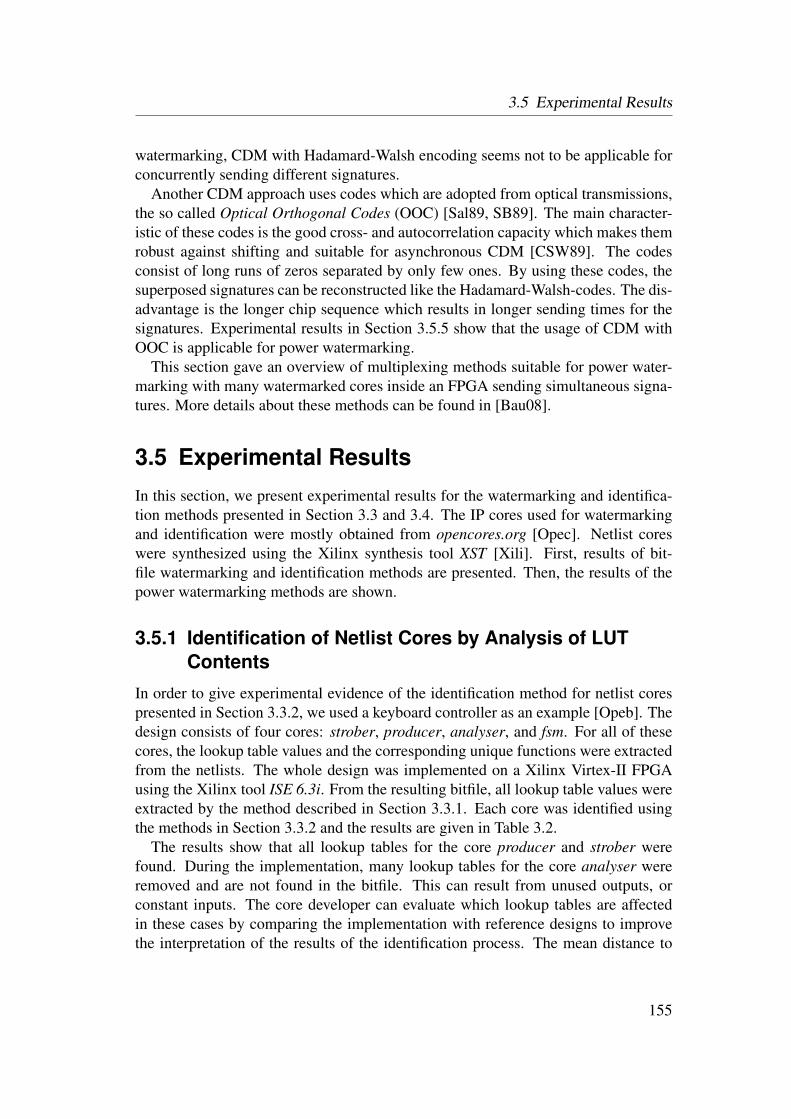
3.5 Experimental Results
watermarking, CDM with Hadamard-Walsh encoding seems not to be applicable forconcurrently sending different signatures.
Another CDM approach uses codes which are adopted from optical transmissions,the so called Optical Orthogonal Codes (OOC) [Sal89, SB89]. The main character-istic of these codes is the good cross- and autocorrelation capacity which makes themrobust against shifting and suitable for asynchronous CDM [CSW89]. The codesconsist of long runs of zeros separated by only few ones. By using these codes, thesuperposed signatures can be reconstructed like the Hadamard-Walsh-codes. The dis-advantage is the longer chip sequence which results in longer sending times for thesignatures. Experimental results in Section 3.5.5 show that the usage of CDM withOOC is applicable for power watermarking.
This section gave an overview of multiplexing methods suitable for power water-marking with many watermarked cores inside an FPGA sending simultaneous signa-tures. More details about these methods can be found in [Bau08].
3.5 Experimental ResultsIn this section, we present experimental results for the watermarking and identifica-tion methods presented in Section 3.3 and 3.4. The IP cores used for watermarkingand identification were mostly obtained from opencores.org [Opec]. Netlist coreswere synthesized using the Xilinx synthesis tool XST [Xili]. First, results of bit-file watermarking and identification methods are presented. Then, the results of thepower watermarking methods are shown.
3.5.1 Identification of Netlist Cores by Analysis of LUTContents
In order to give experimental evidence of the identification method for netlist corespresented in Section 3.3.2, we used a keyboard controller as an example [Opeb]. Thedesign consists of four cores: strober, producer, analyser, and fsm. For all of thesecores, the lookup table values and the corresponding unique functions were extractedfrom the netlists. The whole design was implemented on a Xilinx Virtex-II FPGAusing the Xilinx tool ISE 6.3i. From the resulting bitfile, all lookup table values wereextracted by the method described in Section 3.3.1. Each core was identified usingthe methods in Section 3.3.2 and the results are given in Table 3.2.
The results show that all lookup tables for the core producer and strober werefound. During the implementation, many lookup tables for the core analyser wereremoved and are not found in the bitfile. This can result from unused outputs, orconstant inputs. The core developer can evaluate which lookup tables are affectedin these cases by comparing the implementation with reference designs to improvethe interpretation of the results of the identification process. The mean distance to
155

3. IP Core Watermarking and Identification
Core r q fu found r distance dproducer + strober + fsm + analyser
producer 40 450 3982 40 4.225strober 93 450 3982 93 3.797
fsm 6 450 3982 5 0.883analyser 379 450 3982 217 5.946
Table 3.2: Results for identifying individual cores in a design including four cores.The number of LUT functions used in the core r and in the design q aswell as the number of different unique functions fu are depicted. Thevalues for mean distance to the core center d are in LUT positions.
the calculated core center in all four cases is small. In combination with the highpercentage of found lookup tables, this result supports the assumption that the coreis included in the bitfile. To verify the calculated core centers, we compare the corecenters with the real placement of the slices in the cores. Figure 3.36 shows that thecalculated core center positions correspond with the real positions of the cores.
To evaluate the robustness, we try to find the cores in a bitfile were they were notincluded. For this case, we implemented a Des56 design [Opea] on a Xilinx Virtex-II FPGA and extracted all lookup tables. Table 3.3 shows that the percentage ofthe found lookup tables is low and the mean distance to the calculated core centeris high. These values give evidence that the cores are not included in the design.For a more realistic scenario, we take two cores of the same functionality but froma different developer. For demonstration, a cordic core from Xilinx Coregen [Xilg]and opencores.org [Opec] are taken. We implement the Coregen core into the bitfileand search for the lookup table values from the opencores.org core. Table 3.3 showsthat more than half of the lookup table contents were found, however, the distanceis relatively high. This indicates that the opencores.org core is not included in thebitfile.
3.5.2 Identification of HDL Cores by Analysis of LUTContents
To obtain experimental results for the HDL core identification technique, introducedin Section 3.3.3 we used several cores from opencores.org [Opec]: The cryptographiccores Des56 and 3DES, the processor cores t400, minimips, and 68hc08, as well as thegeneral IP cores LCD, and colorconv. Furthermore, we used different synthesis tools:Xilinx Synthesis Technology (XST) [Xili], precision synthesis from Mentor Graphics[Gra], and Synplify Pro from Synopsis [Synb]. We use the Xilinx Spartan-3 as FPGAtarget technology.
156

3.5 Experimental Results
Figure 3.36: The calculated core centers compared with the real LUT placementsfor the example cores shown in Table 3.2.
Core r q fu found r distance dDes56
producer 40 1574 3982 2 5.55strober 93 1574 3982 44 15.97
fsm 6 1574 3982 3 12.597analyser 379 1574 3982 69 13.865
cordic from Xilinx Coregencordic from opencores 1052 1762 3982 633 26.39
Table 3.3: Results for identifying cores in a design where the cores are not included.First, the cores from the keyboard controller are searched for inclusioninside a Des56 core. The second result stems from trying to identify anopencores.org cordic core in a bitfile containing a Xilinx Coregen cordiccore.
157
3. IP Core Watermarking and Identification
First, we take the same core, synthesized using different synthesis tools and ana-lyze the different resulting lookup table contents. The first step is to map these lookuptable contents into unique functions. For identification, these functions are labeledwith the lowest content value of all lookup table contents which implement the sameunique function. Table 3.4 lists, for example, the unique functions of the core color-conv synthesized with all three synthesis tools. It can be seen that the distribution ofthe most used unique functions is very similar. Only the functions generated by Syn-plify differ slightly from the other tools which can also be seen in the overall numberof used lookup tables.
colorconvNo. LUT inputs unique function XST Precision Synplify
1 2 57 54 602 2 0 18 22 6 312 309 2072 8 0 0 2033 28 0 0 993 2e 48 48 483 ac 144 126 1444 0008 6 15 44 00ac 0 0 154 eefa 0 0 15
overall number of LUTs 579 581 820
Table 3.4: This table shows the different unique functions of the colorconv core syn-thesized with different synthesis tools. All lookup table contents whichimplement the same unique function are mapped to the lowest contentvalue. Note that only functions which appear at least ten times after syn-thesis by one synthesis tool are depicted.
To test the criterion method, we first compare the netlists which implement thesame core, but were synthesized with different synthesis tools. The results are shownin Table 3.5. The value Pa in b denotes to the percentage of the unique functions fromthe core a which can be found in core b. If the criterion value C is bigger thanone, then it is likely that these netlists were synthesized from the same HDL coredescription. This is true for all cores, except of the LCD core where the lookup tablecontent distribution is different for all three synthesis tools.
Next, we compare the lookup table contents of netlists which are generated fromdifferent cores. We compare netlists synthesized with XST or Precision. As it can beseen in Table 3.6, the criterion value C is less than 1 for most cores which indicates
158
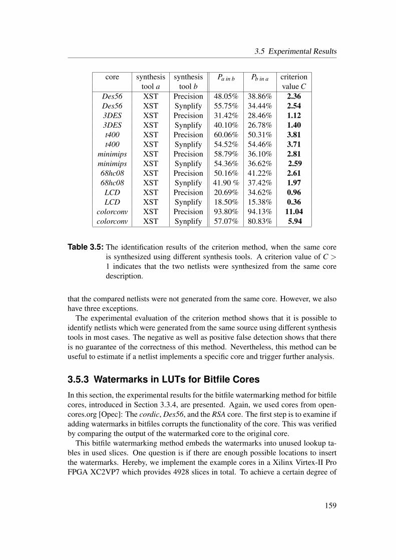
3.5 Experimental Results
core synthesis synthesis Pa in b Pb in a criteriontool a tool b value C
Des56 XST Precision 48.05% 38.86% 2.36Des56 XST Synplify 55.75% 34.44% 2.543DES XST Precision 31.42% 28.46% 1.123DES XST Synplify 40.10% 26.78% 1.40t400 XST Precision 60.06% 50.31% 3.81t400 XST Synplify 54.52% 54.46% 3.71
minimips XST Precision 58.79% 36.10% 2.81minimips XST Synplify 54.36% 36.62% 2.5968hc08 XST Precision 50.16% 41.22% 2.6168hc08 XST Synplify 41.90 % 37.42% 1.97LCD XST Precision 20.69% 34.62% 0.96LCD XST Synplify 18.50% 15.38% 0.36
colorconv XST Precision 93.80% 94.13% 11.04colorconv XST Synplify 57.07% 80.83% 5.94
Table 3.5: The identification results of the criterion method, when the same coreis synthesized using different synthesis tools. A criterion value of C >1 indicates that the two netlists were synthesized from the same coredescription.
that the compared netlists were not generated from the same core. However, we alsohave three exceptions.
The experimental evaluation of the criterion method shows that it is possible toidentify netlists which were generated from the same source using different synthesistools in most cases. The negative as well as positive false detection shows that thereis no guarantee of the correctness of this method. Nevertheless, this method can beuseful to estimate if a netlist implements a specific core and trigger further analysis.
3.5.3 Watermarks in LUTs for Bitfile CoresIn this section, the experimental results for the bitfile watermarking method for bitfilecores, introduced in Section 3.3.4, are presented. Again, we used cores from open-cores.org [Opec]: The cordic, Des56, and the RSA core. The first step is to examine ifadding watermarks in bitfiles corrupts the functionality of the core. This was verifiedby comparing the output of the watermarked core to the original core.
This bitfile watermarking method embeds the watermarks into unused lookup ta-bles in used slices. One question is if there are enough possible locations to insertthe watermarks. Hereby, we implement the example cores in a Xilinx Virtex-II ProFPGA XC2VP7 which provides 4928 slices in total. To achieve a certain degree of
159
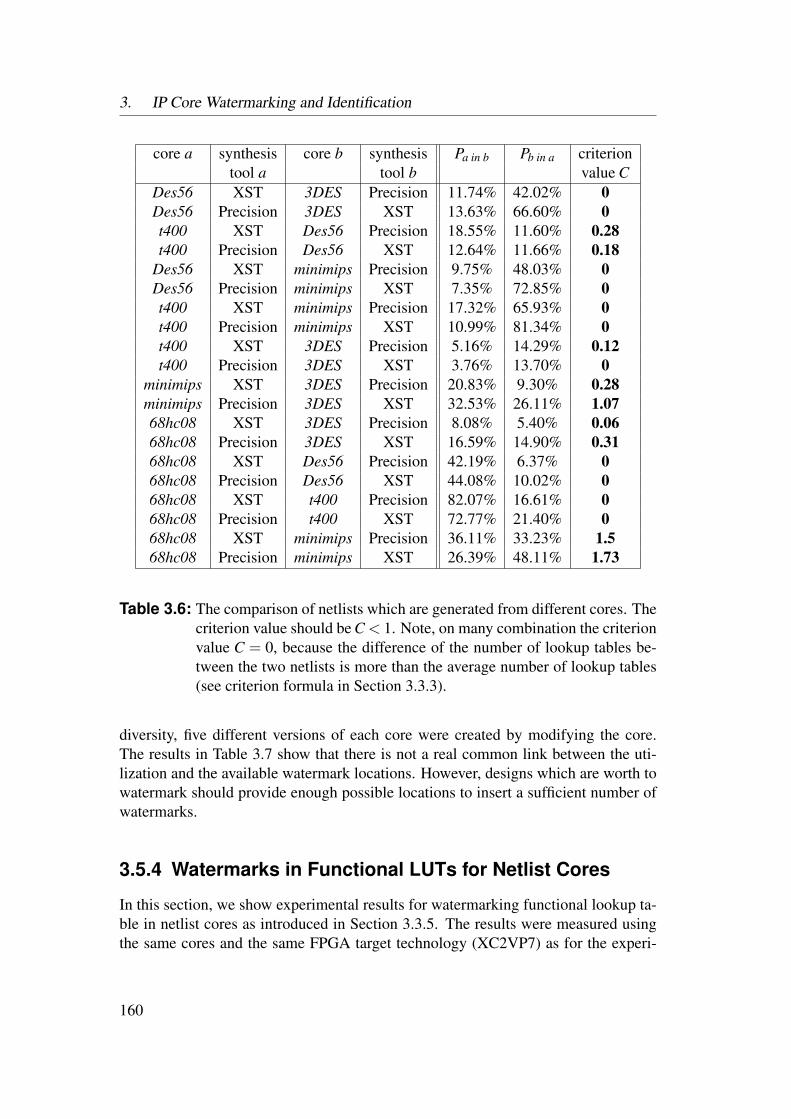
3. IP Core Watermarking and Identification
core a synthesis core b synthesis Pa in b Pb in a criteriontool a tool b value C
Des56 XST 3DES Precision 11.74% 42.02% 0Des56 Precision 3DES XST 13.63% 66.60% 0t400 XST Des56 Precision 18.55% 11.60% 0.28t400 Precision Des56 XST 12.64% 11.66% 0.18
Des56 XST minimips Precision 9.75% 48.03% 0Des56 Precision minimips XST 7.35% 72.85% 0t400 XST minimips Precision 17.32% 65.93% 0t400 Precision minimips XST 10.99% 81.34% 0t400 XST 3DES Precision 5.16% 14.29% 0.12t400 Precision 3DES XST 3.76% 13.70% 0
minimips XST 3DES Precision 20.83% 9.30% 0.28minimips Precision 3DES XST 32.53% 26.11% 1.0768hc08 XST 3DES Precision 8.08% 5.40% 0.0668hc08 Precision 3DES XST 16.59% 14.90% 0.3168hc08 XST Des56 Precision 42.19% 6.37% 068hc08 Precision Des56 XST 44.08% 10.02% 068hc08 XST t400 Precision 82.07% 16.61% 068hc08 Precision t400 XST 72.77% 21.40% 068hc08 XST minimips Precision 36.11% 33.23% 1.568hc08 Precision minimips XST 26.39% 48.11% 1.73
Table 3.6: The comparison of netlists which are generated from different cores. Thecriterion value should be C < 1. Note, on many combination the criterionvalue C = 0, because the difference of the number of lookup tables be-tween the two netlists is more than the average number of lookup tables(see criterion formula in Section 3.3.3).
diversity, five different versions of each core were created by modifying the core.The results in Table 3.7 show that there is not a real common link between the uti-lization and the available watermark locations. However, designs which are worth towatermark should provide enough possible locations to insert a sufficient number ofwatermarks.
3.5.4 Watermarks in Functional LUTs for Netlist Cores
In this section, we show experimental results for watermarking functional lookup ta-ble in netlist cores as introduced in Section 3.3.5. The results were measured usingthe same cores and the same FPGA target technology (XC2VP7) as for the experi-
160
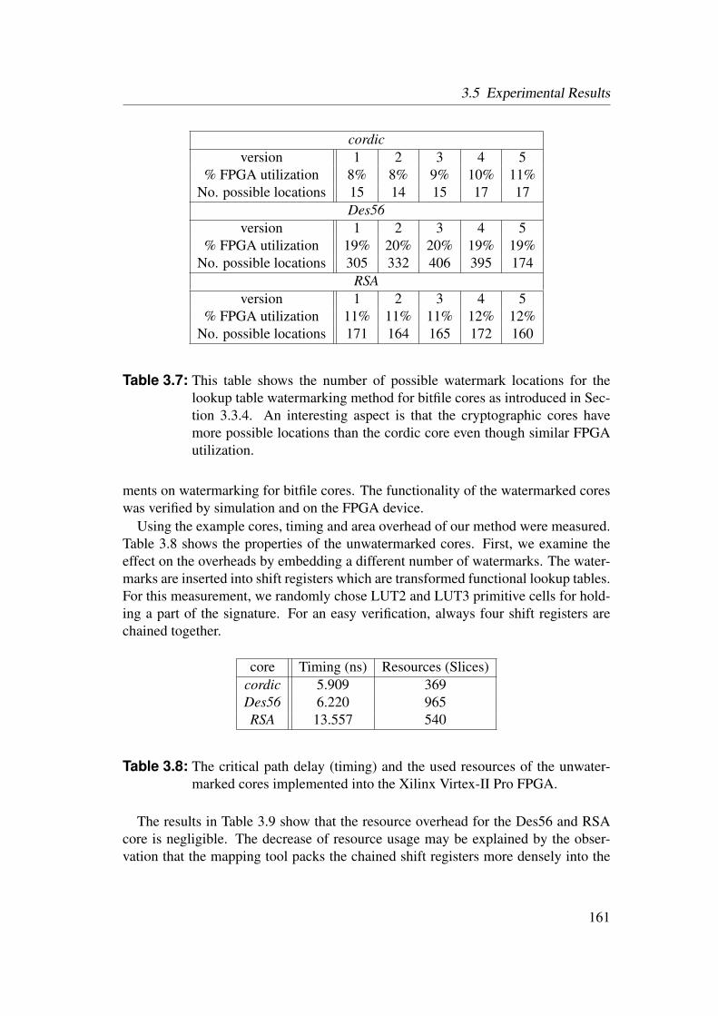
3.5 Experimental Results
cordicversion 1 2 3 4 5
% FPGA utilization 8% 8% 9% 10% 11%No. possible locations 15 14 15 17 17
Des56version 1 2 3 4 5
% FPGA utilization 19% 20% 20% 19% 19%No. possible locations 305 332 406 395 174
RSAversion 1 2 3 4 5
% FPGA utilization 11% 11% 11% 12% 12%No. possible locations 171 164 165 172 160
Table 3.7: This table shows the number of possible watermark locations for thelookup table watermarking method for bitfile cores as introduced in Sec-tion 3.3.4. An interesting aspect is that the cryptographic cores havemore possible locations than the cordic core even though similar FPGAutilization.
ments on watermarking for bitfile cores. The functionality of the watermarked coreswas verified by simulation and on the FPGA device.
Using the example cores, timing and area overhead of our method were measured.Table 3.8 shows the properties of the unwatermarked cores. First, we examine theeffect on the overheads by embedding a different number of watermarks. The water-marks are inserted into shift registers which are transformed functional lookup tables.For this measurement, we randomly chose LUT2 and LUT3 primitive cells for hold-ing a part of the signature. For an easy verification, always four shift registers arechained together.
core Timing (ns) Resources (Slices)cordic 5.909 369Des56 6.220 965RSA 13.557 540
Table 3.8: The critical path delay (timing) and the used resources of the unwater-marked cores implemented into the Xilinx Virtex-II Pro FPGA.
The results in Table 3.9 show that the resource overhead for the Des56 and RSAcore is negligible. The decrease of resource usage may be explained by the obser-vation that the mapping tool packs the chained shift registers more densely into the
161
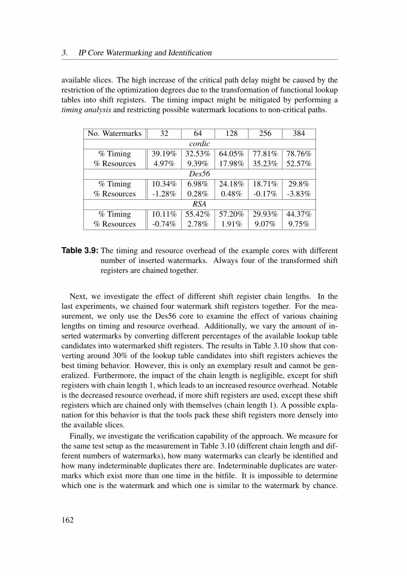
3. IP Core Watermarking and Identification
available slices. The high increase of the critical path delay might be caused by therestriction of the optimization degrees due to the transformation of functional lookuptables into shift registers. The timing impact might be mitigated by performing atiming analysis and restricting possible watermark locations to non-critical paths.
No. Watermarks 32 64 128 256 384cordic
% Timing 39.19% 32.53% 64.05% 77.81% 78.76%% Resources 4.97% 9.39% 17.98% 35.23% 52.57%
Des56% Timing 10.34% 6.98% 24.18% 18.71% 29.8%
% Resources -1.28% 0.28% 0.48% -0.17% -3.83%RSA
% Timing 10.11% 55.42% 57.20% 29.93% 44.37%% Resources -0.74% 2.78% 1.91% 9.07% 9.75%
Table 3.9: The timing and resource overhead of the example cores with differentnumber of inserted watermarks. Always four of the transformed shiftregisters are chained together.
Next, we investigate the effect of different shift register chain lengths. In thelast experiments, we chained four watermark shift registers together. For the mea-surement, we only use the Des56 core to examine the effect of various chaininglengths on timing and resource overhead. Additionally, we vary the amount of in-serted watermarks by converting different percentages of the available lookup tablecandidates into watermarked shift registers. The results in Table 3.10 show that con-verting around 30% of the lookup table candidates into shift registers achieves thebest timing behavior. However, this is only an exemplary result and cannot be gen-eralized. Furthermore, the impact of the chain length is negligible, except for shiftregisters with chain length 1, which leads to an increased resource overhead. Notableis the decreased resource overhead, if more shift registers are used, except these shiftregisters which are chained only with themselves (chain length 1). A possible expla-nation for this behavior is that the tools pack these shift registers more densely intothe available slices.
Finally, we investigate the verification capability of the approach. We measure forthe same test setup as the measurement in Table 3.10 (different chain length and dif-ferent numbers of watermarks), how many watermarks can clearly be identified andhow many indeterminable duplicates there are. Indeterminable duplicates are water-marks which exist more than one time in the bitfile. It is impossible to determinewhich one is the watermark and which one is similar to the watermark by chance.
162
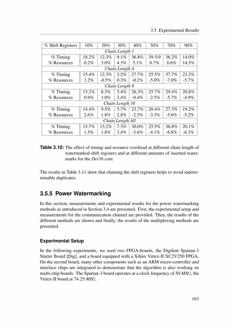
3.5 Experimental Results
% Shift Registers 10% 20% 30% 40% 50% 70% 90%Chain Length 1
% Timing 18.2% 12.3% 9.1% 36.8% 39.%9 36.2% 14.0%% Resources 0.2% 3.0% 4.3% 5.1% 6.7% 8.6% 14.5%
Chain Length 4% Timing 15.4% 12.3% 3.2% 27.7% 25.5% 37.7% 23.2%
% Resources 1.2% -0.5% 0.3% -0.2% -5.0% -7.0% -5.7%Chain Length 8
% Timing 15.2% 8.3% 5.4% 26.3% 25.7% 29.4% 20.8%% Resources 0.9% 1.0% 2.4% -0.4% -2.5% -5.7% -4.9%
Chain Length 16% Timing 14.4% 9.5% 5.7% 23.7% 28.4% 27.3% 19.2%
% Resources 2.6% 1.8% 2.8% -2.5% -3.3% -5.6% -5.2%Chain Length All
% Timing 15.7% 13.2% 7.3% 30.0% 25.5% 36.8% 20.1%% Resources 1.5% 1.8% 3.4% -3.6% -4.1% -6.8% -6.3%
Table 3.10: The effect of timing and resource overhead at different chain length ofwatermarked shift registers and at different amounts of inserted water-marks for the Des56 core.
The results in Table 3.11 show that chaining the shift registers helps to avoid indeter-minable duplicates.
3.5.5 Power Watermarking
In this section, measurements and experimental results for the power watermarkingmethods as introduced in Section 3.4 are presented. First, the experimental setup andmeasurements for the communication channel are provided. Then, the results of thedifferent methods are shown and finally, the results of the multiplexing methods arepresented.
Experimental Setup
In the following experiments, we used two FPGA-boards, the Digilent Spartan-3Starter Board [Dig], and a board equipped with a Xilinx Virtex-II XC2V250 FPGA.On the second board, many other components such as an ARM micro-controller andinterface chips are integrated to demonstrate that the algorithm is also working onmulti-chip boards. The Spartan-3 board operates at a clock frequency of 50 MHz, theVirtex-II board at 74.25 MHz.
163
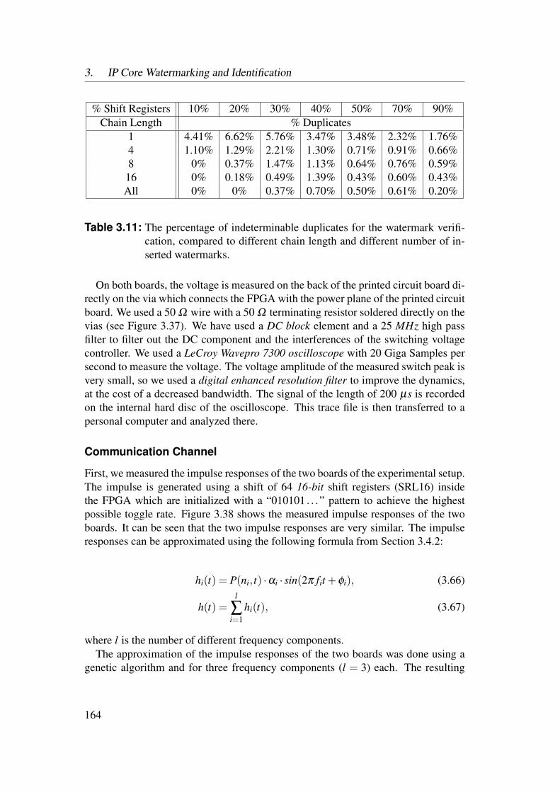
3. IP Core Watermarking and Identification
% Shift Registers 10% 20% 30% 40% 50% 70% 90%Chain Length % Duplicates
1 4.41% 6.62% 5.76% 3.47% 3.48% 2.32% 1.76%4 1.10% 1.29% 2.21% 1.30% 0.71% 0.91% 0.66%8 0% 0.37% 1.47% 1.13% 0.64% 0.76% 0.59%
16 0% 0.18% 0.49% 1.39% 0.43% 0.60% 0.43%All 0% 0% 0.37% 0.70% 0.50% 0.61% 0.20%
Table 3.11: The percentage of indeterminable duplicates for the watermark verifi-cation, compared to different chain length and different number of in-serted watermarks.
On both boards, the voltage is measured on the back of the printed circuit board di-rectly on the via which connects the FPGA with the power plane of the printed circuitboard. We used a 50 Ω wire with a 50 Ω terminating resistor soldered directly on thevias (see Figure 3.37). We have used a DC block element and a 25 MHz high passfilter to filter out the DC component and the interferences of the switching voltagecontroller. We used a LeCroy Wavepro 7300 oscilloscope with 20 Giga Samples persecond to measure the voltage. The voltage amplitude of the measured switch peak isvery small, so we used a digital enhanced resolution filter to improve the dynamics,at the cost of a decreased bandwidth. The signal of the length of 200 µs is recordedon the internal hard disc of the oscilloscope. This trace file is then transferred to apersonal computer and analyzed there.
Communication Channel
First, we measured the impulse responses of the two boards of the experimental setup.The impulse is generated using a shift of 64 16-bit shift registers (SRL16) insidethe FPGA which are initialized with a “010101 . . .” pattern to achieve the highestpossible toggle rate. Figure 3.38 shows the measured impulse responses of the twoboards. It can be seen that the two impulse responses are very similar. The impulseresponses can be approximated using the following formula from Section 3.4.2:
hi(t) = P(ni, t) ·αi · sin(2π fit +φi), (3.66)
h(t) =l
∑i=1
hi(t), (3.67)
where l is the number of different frequency components.The approximation of the impulse responses of the two boards was done using a
genetic algorithm and for three frequency components (l = 3) each. The resulting
164
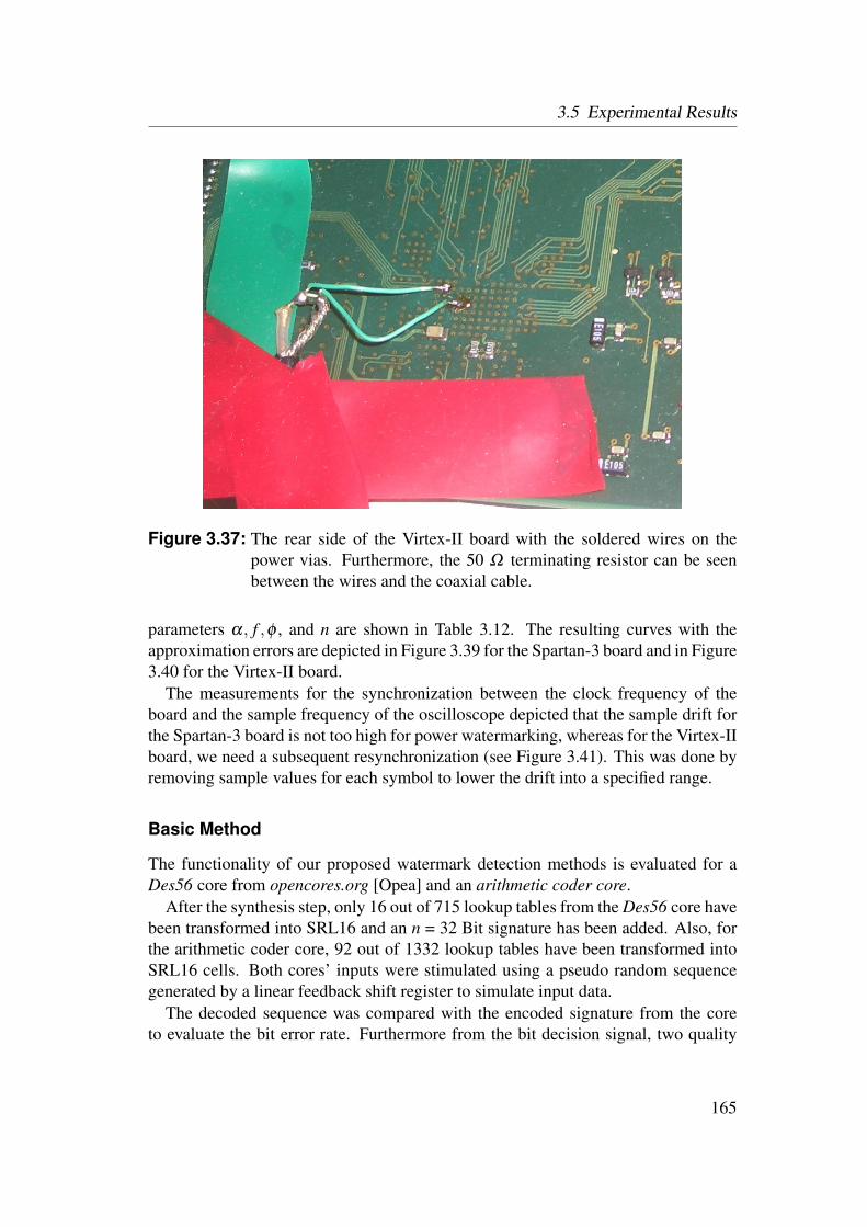
3.5 Experimental Results
Figure 3.37: The rear side of the Virtex-II board with the soldered wires on thepower vias. Furthermore, the 50 Ω terminating resistor can be seenbetween the wires and the coaxial cable.
parameters α, f ,φ , and n are shown in Table 3.12. The resulting curves with theapproximation errors are depicted in Figure 3.39 for the Spartan-3 board and in Figure3.40 for the Virtex-II board.
The measurements for the synchronization between the clock frequency of theboard and the sample frequency of the oscilloscope depicted that the sample drift forthe Spartan-3 board is not too high for power watermarking, whereas for the Virtex-IIboard, we need a subsequent resynchronization (see Figure 3.41). This was done byremoving sample values for each symbol to lower the drift into a specified range.
Basic Method
The functionality of our proposed watermark detection methods is evaluated for aDes56 core from opencores.org [Opea] and an arithmetic coder core.
After the synthesis step, only 16 out of 715 lookup tables from the Des56 core havebeen transformed into SRL16 and an n = 32 Bit signature has been added. Also, forthe arithmetic coder core, 92 out of 1332 lookup tables have been transformed intoSRL16 cells. Both cores’ inputs were stimulated using a pseudo random sequencegenerated by a linear feedback shift register to simulate input data.
The decoded sequence was compared with the encoded signature from the coreto evaluate the bit error rate. Furthermore from the bit decision signal, two quality
165
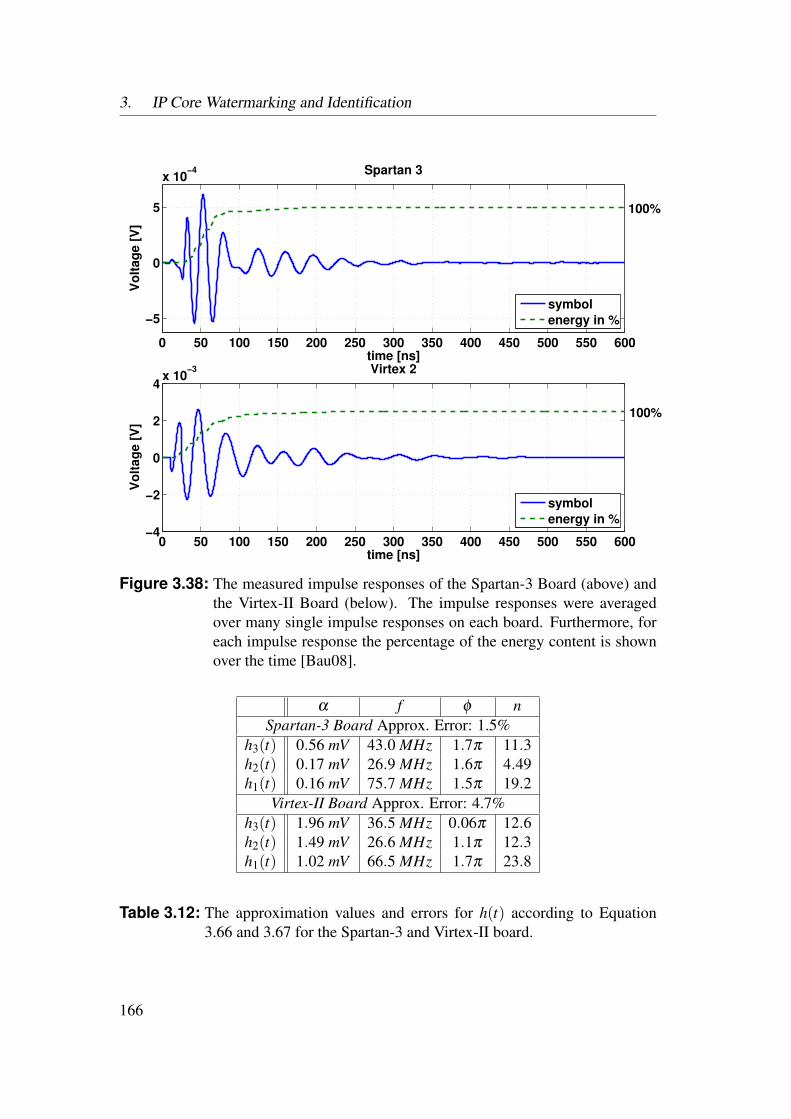
3. IP Core Watermarking and Identification
0 50 100 150 200 250 300 350 400 450 500 550 600
−5
0
5
x 10−4
time [ns]
Vo
lta
ge [
V]
Spartan 3
0 50 100 150 200 250 300 350 400 450 500 550 600−4
−2
0
2
4x 10
−3
time [ns]
Vo
lta
ge
[V
]
Virtex 2
symbol
energy in %
symbol
energy in %
100%
100%
Figure 3.38: The measured impulse responses of the Spartan-3 Board (above) andthe Virtex-II Board (below). The impulse responses were averagedover many single impulse responses on each board. Furthermore, foreach impulse response the percentage of the energy content is shownover the time [Bau08].
α f φ nSpartan-3 Board Approx. Error: 1.5%
h3(t) 0.56 mV 43.0 MHz 1.7π 11.3h2(t) 0.17 mV 26.9 MHz 1.6π 4.49h1(t) 0.16 mV 75.7 MHz 1.5π 19.2
Virtex-II Board Approx. Error: 4.7%h3(t) 1.96 mV 36.5 MHz 0.06π 12.6h2(t) 1.49 mV 26.6 MHz 1.1π 12.3h1(t) 1.02 mV 66.5 MHz 1.7π 23.8
Table 3.12: The approximation values and errors for h(t) according to Equation3.66 and 3.67 for the Spartan-3 and Virtex-II board.
166
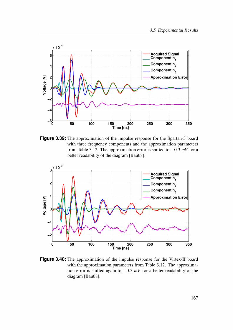
3.5 Experimental Results
0 50 100 150 200 250 300 350−6
−4
−2
0
2
4
6
x 10−4
Time [ns]
Vo
ltag
e [
V]
Acquired SignalComponent h
1
Component h2
Component h3
Approximation Error
Figure 3.39: The approximation of the impulse response for the Spartan-3 boardwith three frequency components and the approximation parametersfrom Table 3.12. The approximation error is shifted to −0.3 mV for abetter readability of the diagram [Bau08].
0 50 100 150 200 250 300 350
−2
−1
0
1
2
3x 10
−3
Time [ns]
Vo
lta
ge
[V
]
Acquired SignalComponent h
1
Component h2
Component h3
Approximation Error
Figure 3.40: The approximation of the impulse response for the Virtex-II boardwith the approximation parameters from Table 3.12. The approxima-tion error is shifted again to −0.3 mV for a better readability of thediagram [Bau08].
167
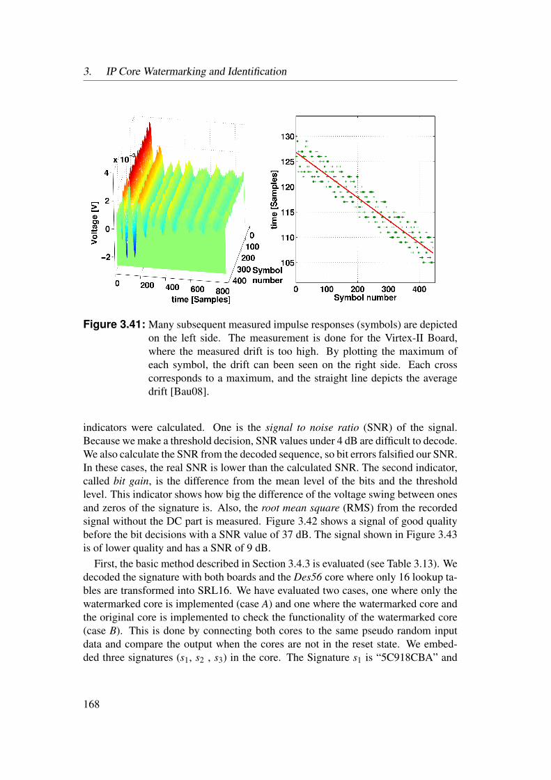
3. IP Core Watermarking and Identification
Figure 3.41: Many subsequent measured impulse responses (symbols) are depictedon the left side. The measurement is done for the Virtex-II Board,where the measured drift is too high. By plotting the maximum ofeach symbol, the drift can been seen on the right side. Each crosscorresponds to a maximum, and the straight line depicts the averagedrift [Bau08].
indicators were calculated. One is the signal to noise ratio (SNR) of the signal.Because we make a threshold decision, SNR values under 4 dB are difficult to decode.We also calculate the SNR from the decoded sequence, so bit errors falsified our SNR.In these cases, the real SNR is lower than the calculated SNR. The second indicator,called bit gain, is the difference from the mean level of the bits and the thresholdlevel. This indicator shows how big the difference of the voltage swing between onesand zeros of the signature is. Also, the root mean square (RMS) from the recordedsignal without the DC part is measured. Figure 3.42 shows a signal of good qualitybefore the bit decisions with a SNR value of 37 dB. The signal shown in Figure 3.43is of lower quality and has a SNR of 9 dB.
First, the basic method described in Section 3.4.3 is evaluated (see Table 3.13). Wedecoded the signature with both boards and the Des56 core where only 16 lookup ta-bles are transformed into SRL16. We have evaluated two cases, one where only thewatermarked core is implemented (case A) and one where the watermarked core andthe original core is implemented to check the functionality of the watermarked core(case B). This is done by connecting both cores to the same pseudo random inputdata and compare the output when the cores are not in the reset state. We embed-ded three signatures (s1, s2 , s3) in the core. The Signature s1 is “5C918CBA” and
168
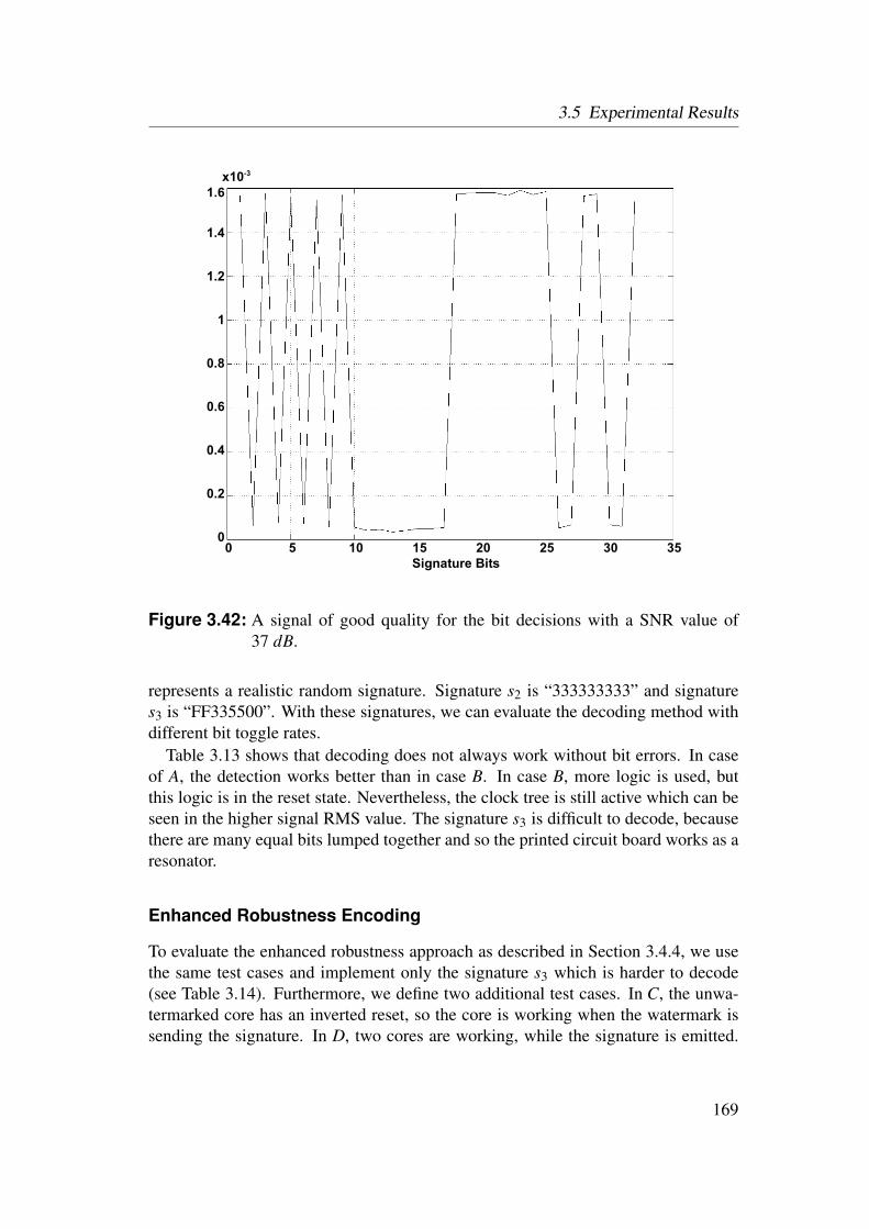
3.5 Experimental Results
25 30 3510 200 5 15Signature Bits
0.8
0.6
1
1.2
1.4
1.6
0.4
0.2
0
x10-3
Figure 3.42: A signal of good quality for the bit decisions with a SNR value of37 dB.
represents a realistic random signature. Signature s2 is “333333333” and signatures3 is “FF335500”. With these signatures, we can evaluate the decoding method withdifferent bit toggle rates.
Table 3.13 shows that decoding does not always work without bit errors. In caseof A, the detection works better than in case B. In case B, more logic is used, butthis logic is in the reset state. Nevertheless, the clock tree is still active which can beseen in the higher signal RMS value. The signature s3 is difficult to decode, becausethere are many equal bits lumped together and so the printed circuit board works as aresonator.
Enhanced Robustness Encoding
To evaluate the enhanced robustness approach as described in Section 3.4.4, we usethe same test cases and implement only the signature s3 which is harder to decode(see Table 3.14). Furthermore, we define two additional test cases. In C, the unwa-termarked core has an inverted reset, so the core is working when the watermark issending the signature. In D, two cores are working, while the signature is emitted.
169
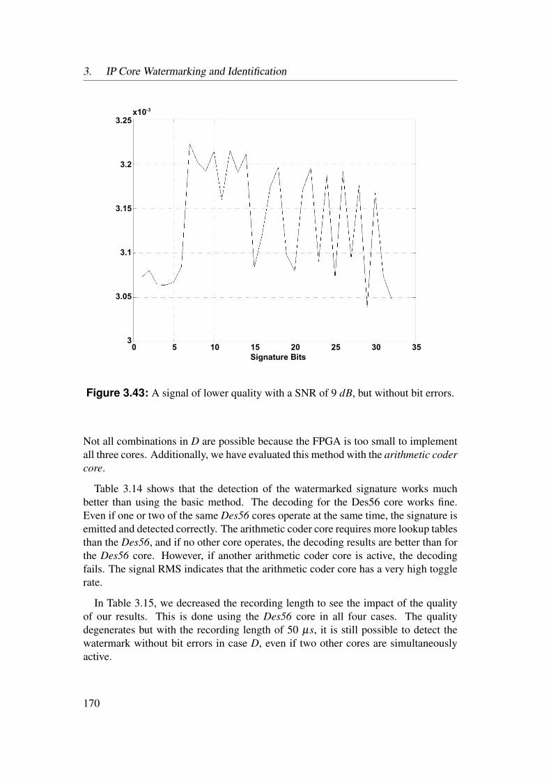
3. IP Core Watermarking and Identification
25 30 3510 200 5 15Signature Bits
3.1
3.15
3.2
3.25
3.05
3
x10-3
3.25
Figure 3.43: A signal of lower quality with a SNR of 9 dB, but without bit errors.
Not all combinations in D are possible because the FPGA is too small to implementall three cores. Additionally, we have evaluated this method with the arithmetic codercore.
Table 3.14 shows that the detection of the watermarked signature works muchbetter than using the basic method. The decoding for the Des56 core works fine.Even if one or two of the same Des56 cores operate at the same time, the signature isemitted and detected correctly. The arithmetic coder core requires more lookup tablesthan the Des56, and if no other core operates, the decoding results are better than forthe Des56 core. However, if another arithmetic coder core is active, the decodingfails. The signal RMS indicates that the arithmetic coder core has a very high togglerate.
In Table 3.15, we decreased the recording length to see the impact of the qualityof our results. This is done using the Des56 core in all four cases. The qualitydegenerates but with the recording length of 50 µs, it is still possible to detect thewatermark without bit errors in case D, even if two other cores are simultaneouslyactive.
170
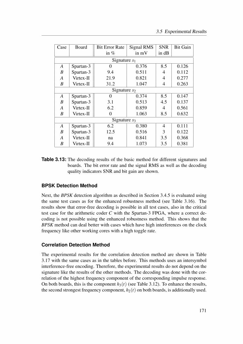
3.5 Experimental Results
Case Board Bit Error Rate Signal RMS SNR Bit Gainin % in mV in dB
Signature s1A Spartan-3 0 0.376 8.5 0.126B Spartan-3 9.4 0.511 4 0.112A Virtex-II 21.9 0.821 4 0.277B Virtex-II 31.2 1.047 4 0.263
Signature s2A Spartan-3 0 0.374 8.5 0.147B Spartan-3 3.1 0.513 4.5 0.137A Virtex-II 6.2 0.859 4 0.561B Virtex-II 0 1.063 8.5 0.632
Signature s3A Spartan-3 6.2 0.380 4 0.111B Spartan-3 12.5 0.516 3 0.122A Virtex-II na 0.841 3.5 0.368B Virtex-II 9.4 1.073 3.5 0.381
Table 3.13: The decoding results of the basic method for different signatures andboards. The bit error rate and the signal RMS as well as the decodingquality indicators SNR and bit gain are shown.
BPSK Detection Method
Next, the BPSK detection algorithm as described in Section 3.4.5 is evaluated usingthe same test cases as for the enhanced robustness method (see Table 3.16). Theresults show that error-free decoding is possible in all test cases, also in the criticaltest case for the arithmetic coder C with the Spartan-3 FPGA, where a correct de-coding is not possible using the enhanced robustness method. This shows that theBPSK method can deal better with cases which have high interferences on the clockfrequency like other working cores with a high toggle rate.
Correlation Detection Method
The experimental results for the correlation detection method are shown in Table3.17 with the same cases as in the tables before. This methods uses an intersymbolinterference-free encoding. Therefore, the experimental results do not depend on thesignature like the results of the other methods. The decoding was done with the cor-relation of the highest frequency component of the corresponding impulse response.On both boards, this is the component h3(t) (see Table 3.12). To enhance the results,the second strongest frequency component, h2(t) on both boards, is additionally used.
171
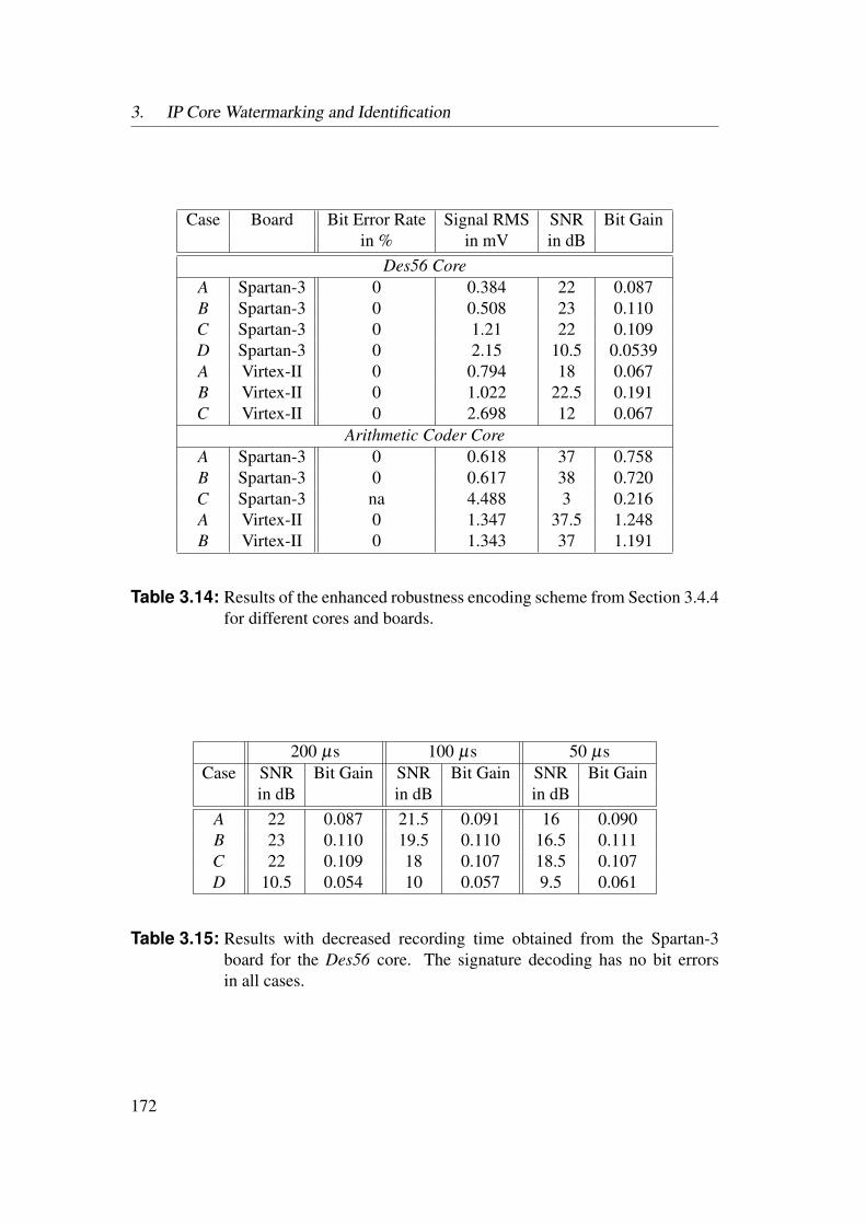
3. IP Core Watermarking and Identification
Case Board Bit Error Rate Signal RMS SNR Bit Gainin % in mV in dB
Des56 CoreA Spartan-3 0 0.384 22 0.087B Spartan-3 0 0.508 23 0.110C Spartan-3 0 1.21 22 0.109D Spartan-3 0 2.15 10.5 0.0539A Virtex-II 0 0.794 18 0.067B Virtex-II 0 1.022 22.5 0.191C Virtex-II 0 2.698 12 0.067
Arithmetic Coder CoreA Spartan-3 0 0.618 37 0.758B Spartan-3 0 0.617 38 0.720C Spartan-3 na 4.488 3 0.216A Virtex-II 0 1.347 37.5 1.248B Virtex-II 0 1.343 37 1.191
Table 3.14: Results of the enhanced robustness encoding scheme from Section 3.4.4for different cores and boards.
200 µs 100 µs 50 µsCase SNR Bit Gain SNR Bit Gain SNR Bit Gain
in dB in dB in dBA 22 0.087 21.5 0.091 16 0.090B 23 0.110 19.5 0.110 16.5 0.111C 22 0.109 18 0.107 18.5 0.107D 10.5 0.054 10 0.057 9.5 0.061
Table 3.15: Results with decreased recording time obtained from the Spartan-3board for the Des56 core. The signature decoding has no bit errorsin all cases.
172
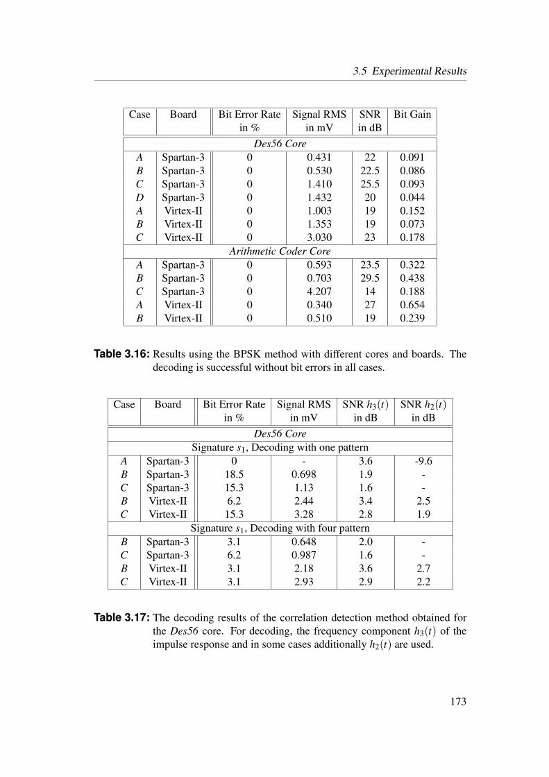
3.5 Experimental Results
Case Board Bit Error Rate Signal RMS SNR Bit Gainin % in mV in dB
Des56 CoreA Spartan-3 0 0.431 22 0.091B Spartan-3 0 0.530 22.5 0.086C Spartan-3 0 1.410 25.5 0.093D Spartan-3 0 1.432 20 0.044A Virtex-II 0 1.003 19 0.152B Virtex-II 0 1.353 19 0.073C Virtex-II 0 3.030 23 0.178
Arithmetic Coder CoreA Spartan-3 0 0.593 23.5 0.322B Spartan-3 0 0.703 29.5 0.438C Spartan-3 0 4.207 14 0.188A Virtex-II 0 0.340 27 0.654B Virtex-II 0 0.510 19 0.239
Table 3.16: Results using the BPSK method with different cores and boards. Thedecoding is successful without bit errors in all cases.
Case Board Bit Error Rate Signal RMS SNR h3(t) SNR h2(t)in % in mV in dB in dB
Des56 CoreSignature s1, Decoding with one pattern
A Spartan-3 0 - 3.6 -9.6B Spartan-3 18.5 0.698 1.9 -C Spartan-3 15.3 1.13 1.6 -B Virtex-II 6.2 2.44 3.4 2.5C Virtex-II 15.3 3.28 2.8 1.9
Signature s1, Decoding with four patternB Spartan-3 3.1 0.648 2.0 -C Spartan-3 6.2 0.987 1.6 -B Virtex-II 3.1 2.18 3.6 2.7C Virtex-II 3.1 2.93 2.9 2.2
Table 3.17: The decoding results of the correlation detection method obtained forthe Des56 core. For decoding, the frequency component h3(t) of theimpulse response and in some cases additionally h2(t) are used.
173
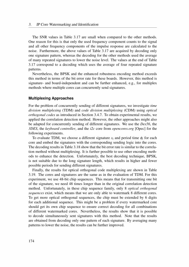
3. IP Core Watermarking and Identification
The SNR values in Table 3.17 are small when compared to the other methods.One reason for this is that only the used frequency component counts to the signaland all other frequency components of the impulse response are calculated to thenoise. Furthermore, the above values of Table 3.17 are acquired by decoding onlyone signature pattern, whereas the decoding for the other methods used the averageof many repeated signatures to lower the noise level. The values at the end of Table3.17 correspond to a decoding which uses the average of four repeated signaturepatterns.
Nevertheless, the BPSK and the enhanced robustness encoding method exceedsthis method in terms of the bit error rate for these boards. However, this method issignature- and board-independent and can be further enhanced, e.g., for multiplexmethods where multiple cores can concurrently send signatures.
Multiplexing Approaches
For the problem of concurrently sending of different signatures, we investigate timedivision multiplexing (TDM) and code division multiplexing (CDM) using opticalorthogonal codes as introduced in Section 3.4.7. To obtain experimental results, weapplied the correlation detection method. However, the other approaches might alsobe adapted for concurrently sending of different signatures. We use the Des56, the3DES, the keyboard controller, and the i2c core from opencores.org [Opec] for thefollowing experiments.
To evaluate TDM, we choose a different signature si and period time φi for eachcore and embed the signatures with the corresponding sending logic into the cores.The decoding results in Table 3.18 show that the bit error rate is similar to the correla-tion method without multiplexing. It is further possible to use other encoding meth-ods to enhance the detection. Unfortunately, the best decoding technique, BPSK,is not suitable due to the long signature length, which results in higher and fewerpossible periods for sending different signatures.
Finally, the results for optical orthogonal code multiplexing are shown in Table3.19. The cores and signatures are the same as in the evaluation of TDM. For thisexperiment, we use 48-bit chip sequences. This means that for transmitting one bitof the signature, we need 48 times longer than in the original correlation detectionmethod. Unfortunately, in these chip sequence family, only 8 optical orthogonalsequences exist, which means that we are only able to watermark 8 different cores.To get more optical orthogonal sequences, the chip must be extended by 6 digitsfor each additional sequence. This might be a problem if every watermarked coreshould get its own chip sequence to ensure correct decoding for all combinationsof different watermarked cores. Nevertheless, the results show that it is possibleto decode simultaneously sent signatures with this method. Note that the resultsare obtained from decoding only one pattern of each signature. By averaging manypatterns to lower the noise, the results can be further improved.
174

3.5 Experimental Results
Bit Error Rate in %Number of period Dec. one Dec. four
Core used SRLs Signature si time φi pattern patternDes56 40 0x153CA9F8 460 µs 9.4 3.13DES 64 0x128E92C1 500 µs 9.4 3.1
keyboard contr. 18 0x928CB241 420 µs 18.3 6.2i2c 25 0x74DE4FC1 380 µs 21.3 6.2
Table 3.18: The decoding results for one pattern and for the average of four patternof the TDM method. All four cores are implemented in one design andsending the corresponding signatures. Furthermore, the number of usedshift registered, converted from functional lookup tables are shown.
Number of Bit Error Rate in %Core used SRLs Chip Sequence h3(t) h3(t)+h2(t)
Des56 40 0xC00000002000 21.9 15.63DES 64 0xA00000400000 15.6 12.5
keyboard contr. 18 0x900010000000 6.25 6.25i2c 25 0x880400000000 18.75 18.75
Table 3.19: The results from applying the code division method using optical or-thogonal codes by sending all signatures simultaneously. The bit errorrates are achieved from decoding only one signature pattern for eachcore.
175
3. IP Core Watermarking and Identification
3.6 Summary
In this chapter, we have presented different approaches for watermarking and iden-tification of IP cores. Our methods follow the strategy of an easy verification of thewatermark or the identification of the core in a bought product from an accused com-pany without any further information. Netlist and HDL cores, which have a hightrade potential for embedded systems developers, are in the focus of our analysis. Weconcentrated on FPGA technology which represents a dynamic and increasing mar-ket. Nevertheless can the methods, especially the power watermarking techniques,also be adapted to ASIC designs.
To establish the authorship in a bought product by watermarking or core identifi-cation, we have discovered different new techniques, how information can be trans-mitted from the embedded core to the outer world. In this work, we concentratedon methods using the FPGA bitfile which can be extracted from the product and onmethods where the signature is transmitted over the power pins of the FPGA.
In Section 3.2, we adapt the theoretical general watermark approach from Li etal. [LMS06] for IP core watermarking and identification and show possible threatsand attacks. Section 3.3 deals with IP core watermarking and identification methodswhere the authorship is established by analysis of the extracted bitfile. The extractionof lookup table contents of a binary bitfile was demonstrated for Xilinx Virtex-II andVirtex-II Pro devices.
Subsequently, we have presented a new method to identify IP cores in FPGA bit-files. Possible transformations of the mapping tools and the effect of the robustnessof the method were discussed. The experimental results show that it is possible toidentify a core inside a design with high probability. The identification process isbased on two parameters, namely the number of found lookup tables of the core inthe design and the mean distance to the core center. However, it must be taken intoaccount that lookup tables of the core may be removed by optimization tools, if a partof the core is not used because the outputs are unconnected or constant values applyto inputs.
Furthermore, methods towards an identification of HDL cores are introduced. Thefirst step is to identify two netlist cores to determine if they were generated from thesame HDL source. Experimental results are promising. However, for a completeapproach for HDL core identification in a product, there are some gaps which mightbe stuffed by future research.
We introduced watermarking methods for bitfile and netlist cores which use a bit-file verification strategy. For bitfile cores, unused lookup tables in used slices carrythe watermark and are easy to extract. For netlist cores, the watermark is insertedinto functional lookup table which have less inputs as the corresponding primitivecell by restricting the reachable address space. By using functional lookup tables, thewatermarks are tightly integrated into the core and prevent the watermarked lookuptables from being removed by either an attacker or synthesis and optimization tools.
176
3.6 Summary
Experimental results show that the watermarks are correctly extractable with highprobability and cause only low overhead.
In Section 3.4, we have presented new watermark techniques for IP cores wherethe signature can be extracted easily over the power pins of the chip. The main ideais that during a reset phase of a chip, a watermark circuit is responsible to emit acharacteristic power pattern sequence that may be measured by voltage fluctuationson power pins. With these techniques, it is possible to decide with high confidence,whether an IP core of a certain vendor is present on th FPGA or not. We have shownhow a watermark can be integrated into a core. For Xilinx FPGAs, it is possible tointegrate the watermark algorithm and the signature into the functionality of the core,so it is hard to remove the watermark, and only very few additional resources arerequired for control. We have investigated also the communication channel from thepower pattern generator inside the core to an oscilloscope which is used to measurethe voltage trace outside the FPGA. A basic algorithm was introduced to detect asignature over the voltage trace of the FPGA, and experimental results have shownthat the functionality of the core is not altered. Also, we introduced an enhanced ro-bustness technique, and a new decoding principle based on BPSK (Binary Phase ShiftKeying) modulation which may improve the decoding quality of the signature evenfurther. Finally, correlation detection was presented which uses special communica-tion channel characteristics to avoid intersymbol interference. With these enhanceddecoding methods, we are able to decode a signature even if other cores are simulta-neously active on the same hardware device and emitting watermark specific powerpattern simultaneously. We also introduced quality indicators to evaluate the resultof the decoded signature and prove the robustness of the techniques.
The experimental results have shown that decoding is possible in all test cases, butit is possible to further improve the quality of the results if more lookup tables aretransformed into shift registers or if the recording time is extended. Additionally, thesignature width might be increased to insert error codes or cyclic redundancy check(CRC) values.
If an FPGA design includes multiple watermarked cores, mutual interference be-tween different signatures may occur, lowering the detection probability. We inves-tigated different multiplexing methods for scenarios where multiple unsynchronizedcores may simultaneously send their signatures. Here, asynchronous time divisionmultiplexing (TDM) which uses different sending periods and code division multi-plexing (CDM) which uses optical orthogonal codes are applicable.
In this chapter, we have presented many novel watermarking methods for differentkinds of cores. Their practical applicability was proven by experiments. For allmethods, we analyzed the strengths and weaknesses in case of removal of ambiguityattacks. Nevertheless, this is a very interesting topic and research is far away frombeing complete or finished.
177

3. IP Core Watermarking and Identification
178
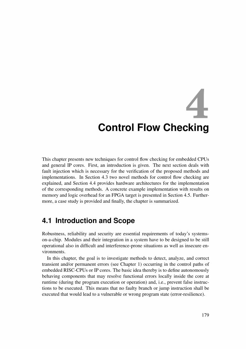
4Control Flow Checking
This chapter presents new techniques for control flow checking for embedded CPUsand general IP cores. First, an introduction is given. The next section deals withfault injection which is necessary for the verification of the proposed methods andimplementations. In Section 4.3 two novel methods for control flow checking areexplained, and Section 4.4 provides hardware architectures for the implementationof the corresponding methods. A concrete example implementation with results onmemory and logic overhead for an FPGA target is presented in Section 4.5. Further-more, a case study is provided and finally, the chapter is summarized.
4.1 Introduction and Scope
Robustness, reliability and security are essential requirements of today’s systems-on-a-chip. Modules and their integration in a system have to be designed to be stilloperational also in difficult and interference-prone situations as well as insecure en-vironments.
In this chapter, the goal is to investigate methods to detect, analyze, and correcttransient and/or permanent errors (see Chapter 1) occurring in the control paths ofembedded RISC-CPUs or IP cores. The basic idea thereby is to define autonomouslybehaving components that may resolve functional errors locally inside the core atruntime (during the program execution or operation) and, i.e., prevent false instruc-tions to be executed. This means that no faulty branch or jump instruction shall beexecuted that would lead to a vulnerable or wrong program state (error-resilience).
179
4. Control Flow Checking
4.1.1 AIS Project OverviewMost of the methods presented in this chapter were developed during the AIS (Au-tonomous Integrated Systems) project funded by the BMBF (German: Bundesmin-isterium fur Bildung und Forschung, Federal Ministry of Education and Research)and the edaCentrum e.V.. The project researches a new approach for reliable MP-SoCs (Multiprocessor-System-on-Chip) which deals with underlying unreliable com-ponents. The approach proposes a new architecture which consists of three logicallayers (see Figure 4.1) [SBE+07b, SBE+07a, SBH+09].
Figure 4.1: On the right side, three behavior levels and the connections betweenthem are shown. On the left side, the flow of modeling and system ex-ploration for autonomic components is depicted [SBE+07b, SBE+07a].
The Three Layer Model
The well known functional layer consists of usual functional elements, like CPUs,special purpose cores, and memories, as well as communication structures, for exam-ple buses.
On the autonomous layer, autonomous elements reside which are able to com-municate to each other over an interconnection structure. The autonomous elementsshall provide monitoring, error detection, and avoidance of failures for the underlying
180

4.1 Introduction and Scope
functional elements. They consist of sensors, evaluators, and actuators which featurethe element to detect and analyze faults, errors, or disturbances of the correspondingfunctional element. In case of an error, they trigger adequate reactions. The com-bination of functional and autonomous elements transform the functional elementsinto reliability-improved autonomous units. The functional and autonomous layersare only logical layers; both are implemented on the same die.
Finally, the third layer is the autonomic operating system layer which consists ofan operating system, running on the different CPUs, which are able to evaluate theinformation from the autonomous elements, and, if necessary, may migrate tasks.
4.1.2 AIS Work Packages Overview
To reach these goals AIS organized its research with two work packages (WP). Anew kind of system design methodology for autonomous integrated systems is ex-plored in the first work package. The second work package introduces the designof components to fulfill the previously named requirements on the component level.With this new component design methodology and components of architecture willbe dimensioned with autonomous characteristics and provided for system design. Ina process of exploration and integration these components will be combined with anautonomous behavior-based operating-system environment at system level. Besidethe hardware design, the new design process will include the operating system levelof the MPSoC.
System Level Techniques (WP1)
The exploration of system level techniques for increased error resiliency consists ofnew design methods, an autonomous operating system, and performance analysis.The research work on system level design methods consists of a transaction-level-based system model which can be explored for the well known optimization goalsperformance, area and power dissipation as well as the introduced new optimiza-tion goal reliability. The focus lies on modeling of degeneration faults which areaccelerated by a huge number of temperature cycles caused by aggressive powermanagement [SSB09].
The distributed autonomous operating system efficiently exploits the restricted re-sources of the MPSoC and provides communication and migration services for eachCPU. To achieve fault tolerance, the operating system generates replicas of services,which come active in the case of a node failure. Also, reliability information fromthe autonomous elements is analyzed and taken into account by the distribution ofservices. If a node becomes unreliable, the services will be migrated to other nodes[BSR09].
If error correction measures are active, they often have impact on the timing andthe performance of the system. The result may be system failures, if deadlines are
181

4. Control Flow Checking
missed and buffers may overflow or underflow. With a sophisticated fault model, theimpact of fault and error correction measures can be simulated and countermeasureslike traffic shaping or a better scheduling can be adapted [SE09].
Component Level Techniques (WP2)
The component level techniques work package of the AIS project analyzes and en-hances exemplarily three common functional components of an MPSoC in order totransform them into autonomous units. The three components are CPU data path,CPU control path, and on-chip communication resources.
The data path of a modern RISC CPU consists of different pipeline stages. Todetect soft errors like single event upsets and transients, a shadow register approachmay be used [ABMF04]. The shadow registers are clocked with a delayed clocksignal whose delay is usually the duration of a soft error effect. To correct a detectederror, history registers are used. Using these registers, the system can perform arollback of one clock cycle to correct the error [BZS+06] (see also Section 4.5.5).
The reliability of the communication resources between different components isas important as the reliability of the components itself. The necessary degree ofreliability depends highly on the type and amount of transferred data. For example,audio or video streams require a lower level of error correction than program data,where a single bit error can cause a system failure. A solution is that for differentcategories of transferred data, different error detection and correction techniques canbe used. Furthermore, error correction measures on a higher level of the protocolstack can be used. At the data link level, e.g., self-calibration and coding techniquesmay be combined to dynamically change the coding strength at runtime [MWB+10].
The methods and techniques discussed in this chapter and elaborated during theproject as part of this dissertation consider the development of concepts for an au-tonomous CPU control path that is able to guarantee the correct execution of thecontrol flow of a given CPU. The main task of the control logic in a CPU is to controlthe program flow. The actual state of execution of a program is in general given bythe state of the program counter and the CPU registers. Usually, the next instructionto fetch is given by an increment of the program counter, but also branches and jumpsmay occur. Now, it is possible to extract information about the program flow fromprogram executable at compile-time and use this information to check the controlflow of the processor with a so called control flow checker unit at runtime (see Figure4.2). If an error is detected, the autonomous control flow checker should be able toinitiate a re-execution of the control flow instruction immediately so to prevent a se-curity bottleneck or guarantee reliable execution of the correct control flow. A quitegeneral definition of the control flow checking may be given as follows:
Definition 4.1 Control flow checking denotes the task of testing whether a sequenceof program counter values is correct with respect to a given program specification.
182

4.2 Fault Injection
Program Counter
Informationfrom thecompiled
code
EmbeddedProcessor
Control FlowChecker
monitor
errorcorrection
Figure 4.2: Concepts for autonomously interacting control flow checking that canmonitor the program counter of a given processor and detect false jumpsor branches based on information in the compiled code. Moreover, thechecker should also be able to correct false jumps and branches.
The main contribution in the context of control flow checking will be concepts,methods, and implementations of novel techniques for autonomous control flow check-ing with the following improvements over the state-of-the-art: Low overhead, detec-tion of all errors which affect the control flow, and modularity.
Prior to presenting results, we discuss the problem of fault injection.
4.2 Fault Injection
This section discusses fault injection which is necessary for the simulation and veri-fication of control flow checking methods. In order to evaluate error detection andcorrection methods, we need to know the failure rate of the system. We can detect afailure, if the output of the system is different from the specification (for example, awrong, unintended or neglected printf() output).
Usually, the MTTF (mean time to failure) is very high in embedded systems, sowe must think of fault injection techniques to stimulate faults. We can inject faultsnaturally or through a fault model.
Natural faults can be injected in a radiation chamber, by applying extreme temper-atures, or through a high excessive clock frequency. The advantage to inject faultsnaturally is that we must not model theses faults. The disadvantage is that normallynot all types of fault can be covered and the equipment can be very expensive. Also, ifwe use FPGAs to demonstrate our methods, the FPGA configuration may be affectedinstead of the logic implemented in the FPGA.
The other option is to use a fault model to stimulate faults. These fault modelscan either be used in RTL system simulation, or be implemented as a fault injection
183
4. Control Flow Checking
component on the chip. Fault injection methods which are using a fault model can becategorized into two classes: Intentional fault injection and random fault injection.
4.2.1 Intentional Fault Injection
Using intentional fault injection, only faults which lead to an error are injected tobe detected by the error detection method. To test a new error detection method,this is usually the first step. If the error detection method works correct, all errorswhich are caused by the faults may be detected and, in the case of an error correctionmethod, also corrected. In the following, some examples of intentional fault injectionfor common embedded systems are given:
Permanent Memory Errors
Permanent memory errors are the result of permanent or transient memory faults, forexample, degeneration, manufacturing faults, SET or SEU inside the memory. To in-ject permanent errors into the memory in embedded systems, an in-circuit debuggercan be used. For example, the in-circuit debugger of the Leon3 [Gaib] system hasunlimited access to the system memory. The program code is written into the systemmemory only once at startup. If the code is manipulated inside the memory, perma-nent memory errors can be simulated. For testing control flow checking methods, itis also easy to manipulate some bits in the control flow instruction in order to the pro-gram counter jumps to an incorrect destination. For simulating permanent memoryfaults, it is also possible to manipulate the executable file (the program binary).
At RTL simulation, the content of the system memory is often stored in a file. Atthis level, it is also very easy to manipulate instructions.
Transient and Permanent On-Chip Errors
Transient and permanent errors in logic and registers inside IP cores can be injectedby altering values of signals. This can be done, for example, for permanent errors(faults) by clamping the signal to ’0’ or ’1’ (stuck at fault). For transient errors,signals can be XORed with an error signal (see Figure 4.3). If the error signal is high,the value of the original signal is inverted. Other possibilities are to take an AND orOR gate instead of the XOR gate to tie a signal up or down. So, SETs and SEUs canbe simulated.
The error signal can be read from a file in the case of RTL simulation, or can begenerated by a PRNG (pseudo random number generator) which can be, for example,an LFSR (linear feedback shift register) or in the trivial case, a counter. Using acounter, the error signal is set high if the counter has reached a specified value. Thesetechniques belong also to the class of intentional fault injection, because the time and
184

4.2 Fault Injection
place were the fault appears is intended. The advantage of the PRNG method is thatit is possible to run an RTL simulation and also implement it on the chip.
Transient On-Chip Faults
To model a SET in RTL simulation, the affected signal is set to high at a specific timeand after the usually time period which a SET affected the signal (usually far fewerthan a clock cycle), the signal is reset to the original value. With this technique, theeffects of a SET can be simulated. The trigger of the injection can also be achievedby a PRNG. Some RTL simulators support the alteration of signals without changingthe VHDL model (for example the force command in Modelsim). This techniquecan also be used to inject faults.
LFSR
fault trigger value
=
XORfault injection module
fast fault injection clock
correct signalcorrupted signal
Figure 4.3: A fault injection module. An LFSR is clocked by a fault injection clockfrom outside the module or internally in case of an RTL simulation. Ifthe LFSR reaches a certain state, a fault is triggered. To inject faults, asignal or net is split, and the fault injection module is inserted.
4.2.2 Random Fault Injection
To measure the reliability of a whole system, it is necessary to evaluate the MTTF.This can be done by using random fault injection. Here, the time and the place (thesignal) where the fault is injected is randomly distributed. To compare the reliabilitywith and without error correction methods, two measurements are necessary, oneusing the error correction module and one without. To get meaningful results, thefaults should be injected in both measurements at the same place and time, so the
185
4. Control Flow Checking
same fault injection configuration should be used. The measurement can be donethrough simulations or in hardware on an FPGA platform.
To inject faults at random, we can use the following strategy: First, the core or thesystem is synthesized and an EDIF netlist is written. A tool chooses signals (or netsfor EDIF netlists) randomly, and inserts fault injection modules (see Figure 4.3) asblack boxes. Afterwards, for simulation, the altered EDIF netlist is converted back toan HDL simulation model. To inject faults on the hardware demonstrator, this step isnot necessary.
Inside the fault injection module, the original signal is combined with an errorsignal using an XOR, AND or OR gate (same technique as in 4.2.1). The error signalis generated either from a file reading module or by a PNRG. To inject a fault in anFPGA demonstrator, only the PNRG method can be used. To inject faults at randomtimes, the PNRG can be initialized with different random values. To inject faultswith a PNRG at a higher time resolution than the clock frequency, a faster clock canbe used for the PNRG. If the PNRG reaches a specified value, a fault injection istriggered. The probability Pf that a fault is injected in a PNRG clock cycle is
Pf =1
2npnrg, (4.1)
where npnrg is the bit width of the PNRG and the trigger value. With the bit widthnpnrg and the number of fault injection modules, different fault probabilities can besimulated.
4.3 Methods for Control Flow CheckingIn this section, new methods for control flow checking in embedded processors andIP cores are presented. First, a classification of control flow instructions in embeddedRISC processors is given. Subsequently, two different methodological concepts forcontrol flow checking of direct jumps and branches are introduced and possibilities tocheck indirect jumps are discussed. Then, methods for repairing a corrupted programpath are proposed. Finally, methods for checking Finite State Machines (FSMs) ingeneral IP cores are analyzed.
4.3.1 Branches and Jumps
Control flow instructions (CFI) can be categorized into conditional branches and un-conditional jumps. Conditional branches depend on the result of a logical or an arith-metic operation. On most processor architectures, the arithmetic operation affects aregister, called integer condition codes (icc). This register consists of flags whichdescribe properties of the result, for example whether the result is greater than zero,or negative. Conditional branches evaluate this register for the decision to take or not
186
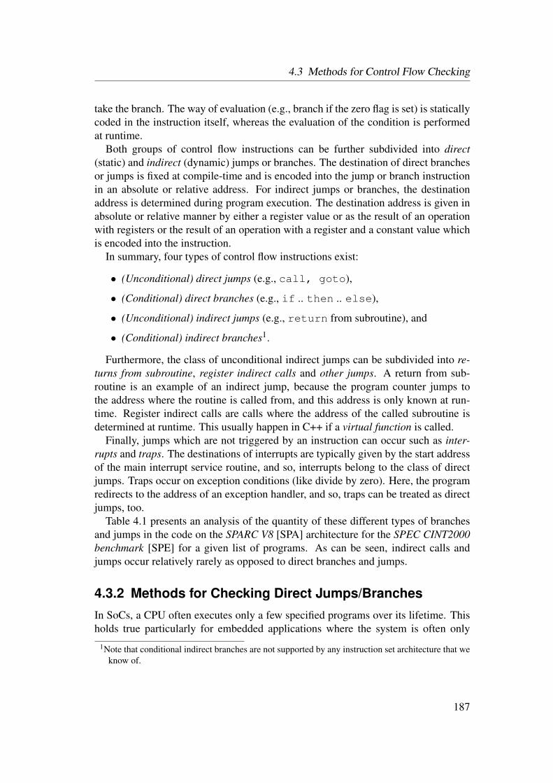
4.3 Methods for Control Flow Checking
take the branch. The way of evaluation (e.g., branch if the zero flag is set) is staticallycoded in the instruction itself, whereas the evaluation of the condition is performedat runtime.
Both groups of control flow instructions can be further subdivided into direct(static) and indirect (dynamic) jumps or branches. The destination of direct branchesor jumps is fixed at compile-time and is encoded into the jump or branch instructionin an absolute or relative address. For indirect jumps or branches, the destinationaddress is determined during program execution. The destination address is given inabsolute or relative manner by either a register value or as the result of an operationwith registers or the result of an operation with a register and a constant value whichis encoded into the instruction.
In summary, four types of control flow instructions exist:
• (Unconditional) direct jumps (e.g., call, goto),
• (Conditional) direct branches (e.g., if .. then .. else),
• (Unconditional) indirect jumps (e.g., return from subroutine), and
• (Conditional) indirect branches1.
Furthermore, the class of unconditional indirect jumps can be subdivided into re-turns from subroutine, register indirect calls and other jumps. A return from sub-routine is an example of an indirect jump, because the program counter jumps tothe address where the routine is called from, and this address is only known at run-time. Register indirect calls are calls where the address of the called subroutine isdetermined at runtime. This usually happen in C++ if a virtual function is called.
Finally, jumps which are not triggered by an instruction can occur such as inter-rupts and traps. The destinations of interrupts are typically given by the start addressof the main interrupt service routine, and so, interrupts belong to the class of directjumps. Traps occur on exception conditions (like divide by zero). Here, the programredirects to the address of an exception handler, and so, traps can be treated as directjumps, too.
Table 4.1 presents an analysis of the quantity of these different types of branchesand jumps in the code on the SPARC V8 [SPA] architecture for the SPEC CINT2000benchmark [SPE] for a given list of programs. As can be seen, indirect calls andjumps occur relatively rarely as opposed to direct branches and jumps.
4.3.2 Methods for Checking Direct Jumps/BranchesIn SoCs, a CPU often executes only a few specified programs over its lifetime. Thisholds true particularly for embedded applications where the system is often only
1Note that conditional indirect branches are not supported by any instruction set architecture that weknow of.
187

4. Control Flow Checking
SPEC all direct indirectprogram instructions branches jumps returns calls other jumps
gzip 19979 1426 599 111 4 0gcc 566280 54791 22446 2236 140 273vpr 51771 2764 2012 269 2 7mcf 3881 288 82 26 0 0
crafty 82891 4814 4074 108 0 13parser 36862 3189 1701 320 0 2
gap 236181 18733 4158 828 1262 5vortex 174567 12537 8491 913 15 21bzip2 12162 748 380 73 0 0twolf 102899 5701 2060 189 0 2
Table 4.1: Accumulated number of all and different kinds of control flow instruc-tions of benchmarks of the SPEC CINT2000 test suite [SPE] when com-piled to the SPARC V8 [SPA] architecture.
programmed once, and the code is never changed during the lifetime of the product,except for the update of the SoC with a new firmware and software. Furthermore, itis well known that in many computational intensive problems, most of the executiontime is spent in only few subroutines. So, it is beneficial to analyze these subroutinesfor branches and jumps statically.
If we assume that only direct jumps and branches exist in a given code segment,we will show that we are able to verify the control flow of this code and guaranteethe correct execution of each direct control flow instruction as well as the (succes-sively) linear execution of all the other instructions (the program counter value isincremented by one word address after each instruction). To verify the correct execu-tion of control flow instructions, we need to check whether the address of the controlflow instruction and the target address are correct. The program counter value beforeand after the execution of a control flow instruction can be compared to these ad-dresses. If there is a mismatch, an error signal is raised. To check a non control flowinstruction, the program counter before and after the execution of the instruction canbe compared. If the second one is not an increment of the first one, the error signal isalso raised.
In the following, we propose two alternative methods to obtain the correct ad-dresses of control flow instructions of a given machine program and the correspond-ing targets. The first method is called basic block or control flow method (CF). Thesecond method is called control flow instruction method (CFI).
188

4.3 Methods for Control Flow Checking
Control Flow Method
First, a given compiled machine code is separated into a set of basic blocks (BB). Abasic block is a sequence of code which is executed successively without any jumpsor branches except, possibly, at the end. The basic block can only be left at the endof a block and can only be entered at the beginning. Only the last instruction can bea jump or branch and only the first instruction can be a jump or branch destination.The following instructions define the beginning of a basic block [TH07]:
• the first instruction in a program or segment,
• the instruction following a control flow instruction,
• the instruction which is a destination of a control flow instruction.
From this information, the control flow graph CFG(BB,T ) is built: Each nodeBBi ∈ BB of the control flow graph represents a basic block. The nodes are sortedwith increasing start address of the corresponding basic block in ascending order.Each edge t j ∈ T represents a transition of the control flow from one basic block toanother. If the last instruction of a basic block BBi is a direct branch instruction, thebasic block has two successors. One is the basic block next in the list BBi+1 (if thebranch is not taken), and to a basic block where the first instruction is the branchdestination (if the branch is taken). Jumps have only one successor, and if the lastinstruction is not a control flow instruction, the successor basic block is always thenext basic block BBi+1. An example program and the corresponding CFG are shownin Figure 4.4 which is separated into basic blocks.
With the given CFG, we have all information to check a sequence of programcounter values for correctness leading to the specification of a proper control flowchecker unit according to Figure 4.2 as follows: The information of the CFG can beeither used to directly define a finite state machine (FSM) to check the correctnessof a sequence of control flow instructions. Alternatively, an implementation usingmicro-instructions of a micro-programmed circuit can be deducted from the CFG.
For an implementation of the checker unit as a micro-programmed circuit, theinformation of the CFG can be stored inside memories. For each basic block, weneed to store the start and the end address and also the indices of the successor basicblocks. The start address of each basic block is the end address of the previous basicblock incremented by one. To minimize the memory overhead, we can store only theend address and a global start address. Also, we only need to store one successor ofa basic block for branches because if the branch is not taken, the basic block with thenext index (BBi+1) is always executed.
With these memory overhead improvements, we need three memory items for eachbasic block inside the memory:
• One for the basic block end address (addr),
189

4. Control Flow Checking
A
B
C
Da
b
c1
2
3
4
5
6
...
for (.. ; ..>.. ; ..)
... if ( .. < .. ) ... ... ...
1
2
3
5
6
4
... cmp .. , .. bg <0x0c> (a) ... cmp .. , .. ble <0x0a> (b) ... ... ... ... b <0x02> (c) ...
0x01
0x030x02
0x04
0x060x05
0x07
0x090x08
0x0a
0x0c0x0b
Figure 4.4: An example program code is given on the left hand side together withthe corresponding assembler code. The CFIs are denoted A to C, andthe CFI destination addresses a to c. D denotes the end of the programor segment to be checked. Furthermore, the code is divided into ba-sic blocks BBi, i = 1, . . . ,6. On the right hand side, the correspondingcontrol flow graph (CFG) is shown.
• one for the index of the branch taken successor basic block (suc), and
• a flag ( f lag) which identifies the type of the last instruction of the basic block.
The flag is needed to choose the right transition to the next basic block (see Figure4.5). Note that if the last instruction of a basic block is not a CFI, the successor basicblock index (suc) is not needed.
The control flow checking algorithm is depicted in C language in Listing 4.1. Forchecking the control flow, we need the current program counter (PC) and the follow-ing program counter (nPC). The algorithm, implemented as a C function, returns 0if the control flow for the program counter and its successor is correct, and −1 ifthe control flow differs from its specification. Further, the index i of the current basicblock and the three memories (addr, suc, and f lag) are needed. The function addr(i)returns the entry with index i of the memory addr.
By looking up the basic block end address in the addr memory (addr(i)), we knowwhen the basic block end is reached (Line 3). If the basic block end is not reached,the address of the next program counter must be the current address incremented byone (Line 23). If not, an error occurs. If the basic block end is reached, we mustdistinguish between the different types of the last instruction inside the basic block(Line 4, 9, and 17). If this is an unconditional jump, like a call, only the jump
190

4.3 Methods for Control Flow Checking
addr suc flag
0x010x030x060x090x0b0x0c
-65-2-
NBBNJN
index
123456
Figure 4.5: Three memory areas are necessary to store required information foreach CFG. In the first column (addr), the address of the last instruc-tion of the basic block is stored. The successor basic block for a takenbranch is stored in the second column (suc). In the third column ( f lag),a flag is stored which identifies the type of the last instruction of a basicblock. An N denotes a non control flow instruction, whereas a B de-notes a branch. This example memory stores the values for the exampleprogram in Figure 4.4.
target must be checked for correctness. The corresponding target address is the startaddress of the successor basic block, given by its index. To get this address, theend address of the basic block with the previous index is fetched and the address isincremented (BBi−1 +1 or Line 5). Furthermore, the current index i must be updatedto the successor basic block index (Line 6). If the last basic block instruction isa conditional branch, two possible successor basic blocks exist. If the branch istaken (Line 10), the handling is the same as for an unconditional jump. If the branchis not taken (Line 13), the next program counter value should be the current valueincremented by one (nPC == PC + 1). Hence, the next instruction belongs to thesuccessive basic block and also the basic block index i must be updated (Line 14).Finally, if the last instruction of a basic block is not a CFI, the checking behavior isthe same as on conditional branches, where the branch is not taken (Line 18).
One very similar approach of a CF method is described in [ARRJ06]. Here, theCFG is implemented in hardware by a finite state machine and a lookup table forresolving the control flow instruction addresses and indices (in memory). The disad-vantage of this approach is that the checker unit must be synthesized new for eachprogram. Here, in our memory-based approach, only the contents of the memoriesneed to be reconfigured in order to check a new program.
191
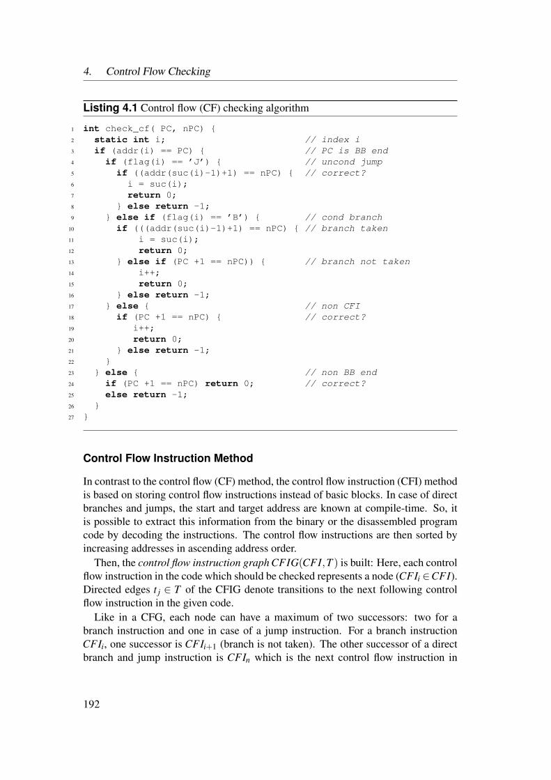
4. Control Flow Checking
Listing 4.1 Control flow (CF) checking algorithm
1 int check_cf( PC, nPC) 2 static int i; // index i3 if (addr(i) == PC) // PC is BB end4 if (flag(i) == ’J’) // uncond jump5 if ((addr(suc(i)-1)+1) == nPC) // correct?6 i = suc(i);7 return 0;8 else return -1;9 else if (flag(i) == ’B’) // cond branch
10 if (((addr(suc(i)-1)+1) == nPC) // branch taken11 i = suc(i);12 return 0;13 else if (PC +1 == nPC)) // branch not taken14 i++;15 return 0;16 else return -1;17 else // non CFI18 if (PC +1 == nPC) // correct?19 i++;20 return 0;21 else return -1;22 23 else // non BB end24 if (PC +1 == nPC) return 0; // correct?25 else return -1;26 27
Control Flow Instruction Method
In contrast to the control flow (CF) method, the control flow instruction (CFI) methodis based on storing control flow instructions instead of basic blocks. In case of directbranches and jumps, the start and target address are known at compile-time. So, itis possible to extract this information from the binary or the disassembled programcode by decoding the instructions. The control flow instructions are then sorted byincreasing addresses in ascending address order.
Then, the control flow instruction graph CFIG(CFI,T ) is built: Here, each controlflow instruction in the code which should be checked represents a node (CFIi ∈CFI).Directed edges t j ∈ T of the CFIG denote transitions to the next following controlflow instruction in the given code.
Like in a CFG, each node can have a maximum of two successors: two for abranch instruction and one in case of a jump instruction. For a branch instructionCFIi, one successor is CFIi+1 (branch is not taken). The other successor of a directbranch and jump instruction is CFIn which is the next control flow instruction in
192
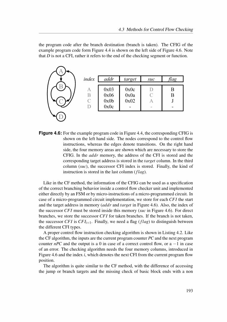
4.3 Methods for Control Flow Checking
the program code after the branch destination (branch is taken). The CFIG of theexample program code form Figure 4.4 is shown on the left side of Figure 4.6. Notethat D is not a CFI, rather it refers to the end of the checking segment or function.
A
B
C
D
addr suc flag
0x030x060x0b0x0c
DCA-
BBJ-
index
ABCD
target
0x0c0x0a0x02-
Figure 4.6: For the example program code in Figure 4.4, the corresponding CFIG isshown on the left hand side. The nodes correspond to the control flowinstructions, whereas the edges denote transitions. On the right handside, the four memory areas are shown which are necessary to store theCFIG. In the addr memory, the address of the CFI is stored and thecorresponding target address is stored in the target column. In the thirdcolumn (suc), the successor CFI index is stored. Finally, the kind ofinstruction is stored in the last column ( f lag).
Like in the CF method, the information of the CFIG can be used as a specificationof the correct branching behavior inside a control flow checker unit and implementedeither directly by an FSM or by micro-instructions of a micro-programmed circuit. Incase of a micro-programmed circuit implementation, we store for each CFI the startand the target address in memory (addr and target in Figure 4.6). Also, the index ofthe successor CFI must be stored inside this memory (suc in Figure 4.6). For directbranches, we store the successor CFI for taken branches. If the branch is not taken,the successor CFI is CFIi+1. Finally, we need a flag ( f lag) to distinguish betweenthe different CFI types.
A proper control flow instruction checking algorithm is shown in Listing 4.2. Likethe CF algorithm, the inputs are the current program counter PC and the next programcounter nPC and the output is a 0 in case of a correct control flow, or a −1 in caseof an error. The checking algorithm needs the four memory columns, introduced inFigure 4.6 and the index i, which denotes the next CFI from the current program flowposition.
The algorithm is quite similar to the CF method, with the difference of accessingthe jump or branch targets and the missing check of basic block ends with a non
193
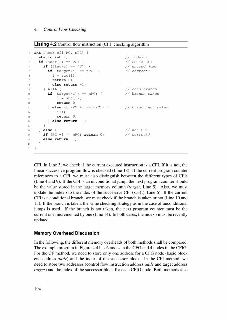
4. Control Flow Checking
Listing 4.2 Control flow instruction (CFI) checking algorithm
1 int check_cfi(PC, nPC) 2 static int i; // index i3 if (addr(i) == PC) // PC is CFI4 if (flag(i) == ’J’) // uncond jump5 if (target(i) == nPC) // correct?6 i = suc(i);7 return 0;8 else return -1;9 else // cond branch
10 if (target(i)) == nPC) // branch taken11 i = suc(i);12 return 0;13 else if (PC +1 == nPC)) // branch not taken14 i++;15 return 0;16 else return -1;17 18 else // non CFI19 if (PC +1 == nPC) return 0; // correct?20 else return -1;21 22
CFI. In Line 3, we check if the current executed instruction is a CFI. If it is not, thelinear successive program flow is checked (Line 18). If the current program counterreferences to a CFI, we must also distinguish between the different types of CFIs(Line 4 and 9). If the CFI is an unconditional jump, the next program counter shouldbe the value stored in the target memory column (target, Line 5). Also, we mustupdate the index i to the index of the successive CFI (suc(i), Line 6). If the currentCFI is a conditional branch, we must check if the branch is taken or not (Line 10 and13). If the branch is taken, the same checking strategy as in the case of unconditionaljumps is used. If the branch is not taken, the next program counter must be thecurrent one, incremented by one (Line 14). In both cases, the index i must be recentlyupdated.
Memory Overhead Discussion
In the following, the different memory overheads of both methods shall be compared.The example program in Figure 4.4 has 6 nodes in the CFG and 4 nodes in the CFIG.For the CF method, we need to store only one address for a CFG node (basic blockend address addr) and the index of the successor block. In the CFI method, weneed to store two addresses (control flow instruction address addr and target addresstarget) and the index of the successor block for each CFIG node. Both methods also
194
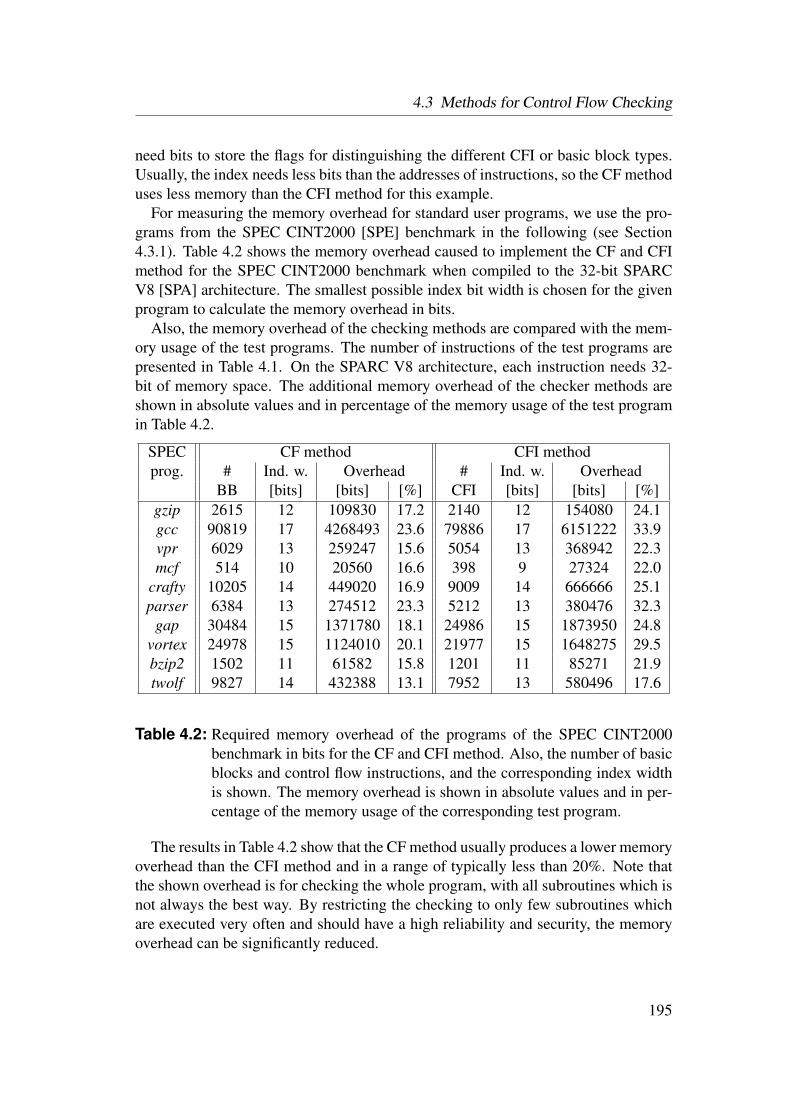
4.3 Methods for Control Flow Checking
need bits to store the flags for distinguishing the different CFI or basic block types.Usually, the index needs less bits than the addresses of instructions, so the CF methoduses less memory than the CFI method for this example.
For measuring the memory overhead for standard user programs, we use the pro-grams from the SPEC CINT2000 [SPE] benchmark in the following (see Section4.3.1). Table 4.2 shows the memory overhead caused to implement the CF and CFImethod for the SPEC CINT2000 benchmark when compiled to the 32-bit SPARCV8 [SPA] architecture. The smallest possible index bit width is chosen for the givenprogram to calculate the memory overhead in bits.
Also, the memory overhead of the checking methods are compared with the mem-ory usage of the test programs. The number of instructions of the test programs arepresented in Table 4.1. On the SPARC V8 architecture, each instruction needs 32-bit of memory space. The additional memory overhead of the checker methods areshown in absolute values and in percentage of the memory usage of the test programin Table 4.2.
SPEC CF method CFI methodprog. # Ind. w. Overhead # Ind. w. Overhead
BB [bits] [bits] [%] CFI [bits] [bits] [%]gzip 2615 12 109830 17.2 2140 12 154080 24.1gcc 90819 17 4268493 23.6 79886 17 6151222 33.9vpr 6029 13 259247 15.6 5054 13 368942 22.3mcf 514 10 20560 16.6 398 9 27324 22.0
crafty 10205 14 449020 16.9 9009 14 666666 25.1parser 6384 13 274512 23.3 5212 13 380476 32.3
gap 30484 15 1371780 18.1 24986 15 1873950 24.8vortex 24978 15 1124010 20.1 21977 15 1648275 29.5bzip2 1502 11 61582 15.8 1201 11 85271 21.9twolf 9827 14 432388 13.1 7952 13 580496 17.6
Table 4.2: Required memory overhead of the programs of the SPEC CINT2000benchmark in bits for the CF and CFI method. Also, the number of basicblocks and control flow instructions, and the corresponding index widthis shown. The memory overhead is shown in absolute values and in per-centage of the memory usage of the corresponding test program.
The results in Table 4.2 show that the CF method usually produces a lower memoryoverhead than the CFI method and in a range of typically less than 20%. Note thatthe shown overhead is for checking the whole program, with all subroutines which isnot always the best way. By restricting the checking to only few subroutines whichare executed very often and should have a high reliability and security, the memoryoverhead can be significantly reduced.
195
4. Control Flow Checking
Instruction Integrity Checker
The instruction integrity checker (IIC) is an extension to the control flow method tocheck all types of instructions, not only control flow instructions. A CRC (cyclicredundancy check) or hash value may be calculated offline for all instructions insidea basic block (at compile-time) and online inside the checker unit [MLS91]. Theoffline calculated CRCs are stored inside an additional memory which extends theother checker memories (see Figure 4.5). For each basic block, we store the endaddress addr, the index of the next basic block suc (for a jump or a taken branch),the flags f lag and additionally the CRC or hash value in the memory iic (instructionintegrity check).
The checker unit calculates a CRC from the instructions during the execution ofa basic block. At the last instruction of the basic block, the calculated CRC can becompared with the offline calculated CRC, stored inside the iic memory. If the CRCsare not equal, one or more bits are false in the instruction stream. This error can besignaled to the operating system by an interrupt or the system might be rebooted bya hardware reset. A re-execution or correction is not or hardly possible, because weare able to detect an error inside a basic block only at the end of the block.
The instruction integrity checking is not applicable for the CFI method, becausethere may exist more than one path to a CFI node, whereas in the CF method a basicblock is always traversed on the same path. As an example, consider the if clausein the program in Figure 4.4. In the CF method, if the branch (if) is not taken, onlybasic block 5 is traversed. If the branch is taken, basic blocks 4 and 5 is transversed,but basic block 5 is executed on the same way as if the branch was not taken. Unlikein the CFI method, if the branch is taken or not, always the CFI C is the successor.However, through the way to C the program flow takes different paths, depending onwhether the branch is taken or not.
Walking through different paths to a node results in different CRC or hash values.With the IIC method, we are only able to store one CRC or hash value in the addi-tional memory column for one node. Surely, we could extend the memory to store avalue for each possible path, but this would result in a huge memory overhead, be-cause we must reserve memory space for each node. This shows that the instructionintegrity checker is not practical to the CFI method.
Conclusions
Both introduced methods can only check direct branches and jumps, where start anddestination addresses can be extracted from the compiled code.
The advantage of the CF method is that in most cases, fewer additional memoryresources are needed than for the CFI method. The disadvantage of the CF method isthat memory handling is more difficult. On many processor architectures, the fastestexecution of one instruction is one clock cycle. Consider Algorithm 4.1, where we
196
4.3 Methods for Control Flow Checking
need access to the addr memory for each control flow instruction twice, once for theend address of the basic block (Line 3) and once for the start address of the successorbasic block (Line 5 and 10). To achieve this in a single clock cycle, we need adual-port memory which is more expensive than single port memories. Furthermore,for the second access to the memory, we need first the successor index from thesuc memory. To do both memory accesses in one clock cycle is nearly impossibleon high-clocked processors. Furthermore, the access to the suc memory cannot bescheduled one clock cycle before, because if the current basic block consists onlyof one instruction, and the previous basic block ends with a branch instruction, thecurrent index i depends on the result of the executed branch (taken or not). This showsus that we need at least two clock cycles to check a transition in CFG. To ensure thaton a basic block end the correct start and destination addresses are available, wemight pre-read both values. This can also be done with a single ported addr memory.On the first clock cycle, the basic block end address is read from the addr memoryand the successor basic block index is read from the suc memory. On the secondclock cycle, the target address is read from the addr. But this pre-read can only bedone if the basic block consists of more than one instruction. If a basic block consistsof only one instruction, we must stall the processor pipeline to verify the control flowinstruction to prevent possible erroneous behavior. Fortunately, basic blocks withonly one instruction are very rare.
The CFI method, on the other hand, requires only one memory access for eachmemory. In Line 3 of the Algorithm 4.2, we access the addr memory to get the nextCFI address. In the same clock cycle we can access the target memory to fetch thecorrect destination address (Line 5 and 10). With the CFI method, it is possible tocheck a transition in the CFI graph with at least one clock cycle. Therefore, the CFImethod has no execution time overhead at all.
The advantages of the CFI method are that the checker unit is very simple and usesonly few logic resources. Also, we have no performance impact, because the correctcontrol flow instruction address and target address may be loaded from the memoryin a single clock cycle. The disadvantages are that usually more memory resourcesare needed as for the CF method and that we are not able to check the integrity of noncontrol flow instructions.
Finally, both introduced concepts for control flow checking have the big advantageover [ARRJ06] in being reprogrammable. Thus, only the memory of the controlflow checker unit needs to be reprogrammed so to check a different program. Noadjustments of the hardware are thus necessary. Moreover, we have no performanceimpact for verify the control flow like the software-based methods.
4.3.3 Methods for Checking Indirect Jumps/BranchesChecking indirect jumps or branches is more difficult than direct branches or jumps,because the jump destination cannot be determined from the compiled program code.
197
4. Control Flow Checking
In fact, according to the instruction specification of indirect jumps, all possible targetswhich are inside the reachable area of the jump, are allowed. From the hardwareside, also a falsified indirect CFI which jumps to a wrong address is in accordance tothe processor specification. Almost all code injection attacks target this behavior bymanipulating indirect jump targets (the return stack). However, from the software orlogical side, there are certainly some restrictions of indirect jump targets: Compilersuse indirect jumps in a stylized manner which can be analyzed [LB94]. Almost allindirect jumps which are compiled from a modern program language, like C, C++,or Java, are returns from subroutine, or either belong to a switch case clause,which is implemented using a jump table, or are indirect calls which are mainly usedin object-oriented languages, like C++ or Java. Indirect jumps which appear in hand-written code are nearly impossible to analyze. Fortunately, hand-written assemblercode is used more and more rarely today.
The results reported in Table 4.1 show that returns from subroutine are clearly themain usage of indirect jumps. Upon a call, the address of the back-jump is storedinside a register or a memory stack, and on a return from subroutine, a back-jump tothis address is initiated.
Indirect jumps are also used for jump tables to efficiently implement switchcase clauses. Here, the alternative case targets are assembled in a jump tablewhich is addressed by the previously calculated operator. Furthermore, the targetsmay be direct jumps which lead the control flow to the desired code segment (seeFigure 4.7). Another way to use a jump table is to call different functions, dependingon an input. Here, the alternative function pointers are stored inside a jump table,whereas the index of the table is calculated with the input value. The address of thedesired function is fetched from the table and is called with an indirect jump. Notethat jump tables are not often used by compilers. Usually, switch case clausesare translated to an if .. else if tree. But, depending on the compiler andoptimization parameters, indirect jumps might nevertheless occur. Indirect jumpswhich result from jump table implementations are listed in Table 4.1 under the cate-gory “other jumps”.
Finally, the indirect jumps are also used as indirect calls (see Table 4.1). Duringindirect calls, the address of the target function is loaded inside a register and with anindirect jump the function will be called. This occurs mainly in object-oriented pro-gramming languages that support function pointers and virtual functions. However,functions called by a jump table also use indirect calls.
The methods for checking indirect jumps that will be described in the followingcan be categorized into methods using information which are gathered by analysis orsimulation at compile-time and methods which are only using runtime information.
198
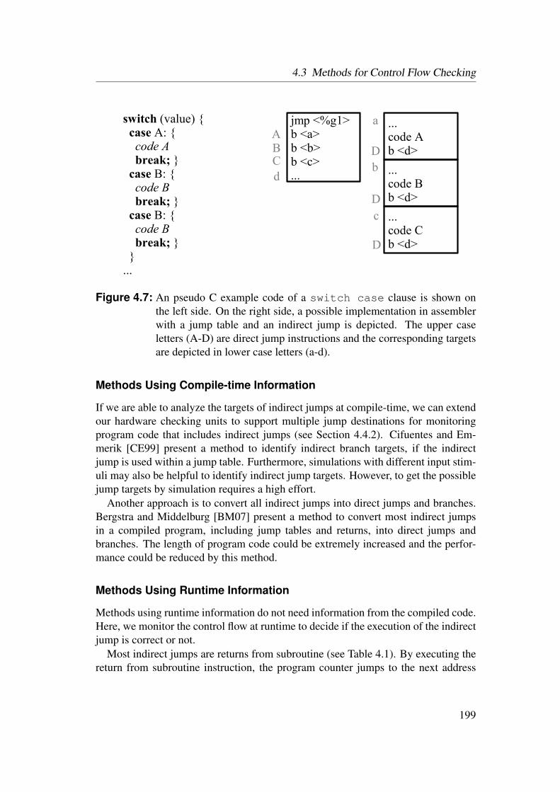
4.3 Methods for Control Flow Checking
ABC
D
a
b
c
jmp <%g1> b <a> b <b> b <c> ...
... code A b <d>
d ... code B b <d>
... code C b <d>
D
D
switch (value) case A: code A break; case B: code B break; case B: code B break; ...
Figure 4.7: An pseudo C example code of a switch case clause is shown onthe left side. On the right side, a possible implementation in assemblerwith a jump table and an indirect jump is depicted. The upper caseletters (A-D) are direct jump instructions and the corresponding targetsare depicted in lower case letters (a-d).
Methods Using Compile-time Information
If we are able to analyze the targets of indirect jumps at compile-time, we can extendour hardware checking units to support multiple jump destinations for monitoringprogram code that includes indirect jumps (see Section 4.4.2). Cifuentes and Em-merik [CE99] present a method to identify indirect branch targets, if the indirectjump is used within a jump table. Furthermore, simulations with different input stim-uli may also be helpful to identify indirect jump targets. However, to get the possiblejump targets by simulation requires a high effort.
Another approach is to convert all indirect jumps into direct jumps and branches.Bergstra and Middelburg [BM07] present a method to convert most indirect jumpsin a compiled program, including jump tables and returns, into direct jumps andbranches. The length of program code could be extremely increased and the perfor-mance could be reduced by this method.
Methods Using Runtime Information
Methods using runtime information do not need information from the compiled code.Here, we monitor the control flow at runtime to decide if the execution of the indirectjump is correct or not.
Most indirect jumps are returns from subroutine (see Table 4.1). By executing thereturn from subroutine instruction, the program counter jumps to the next address
199
4. Control Flow Checking
after the instruction, were the subroutine was called. The return address is typicallystored in a register inside the CPU so the return instruction is a special indirect jump.Returns can be verified by implementing an additional hardware stack [KE91]. On acall (direct or indirect), the return address is stored in the stack and when the returninstruction is executed, the back-jump can be verified.
Furthermore, indirect branch prediction units can be used to evaluate an indirectjump address. Branch prediction is used in pipelined processors to avoid pipelinestalls on branches. A prediction is made if a branch will be taken or not and the nextinstructions will be fetched according to the prediction. If the prediction was right,no stall occurs, if not, the pipeline must be stalled and the right instructions must befetched.
Indirect branch prediction units predict destinations of indirect jumps. The predic-tions are made based on the jump behavior in the past [CHP97, SFF+02, JMKP07].The result of an indirect branch predict unit might be used to evaluate how reliablethe jump destination is. If the prediction is correct, then the probability that this jumpis correct is high, but if the prediction is incorrect, the jump destination could be false.A non-predicted indirect jump target has a lower trustworthiness. With this method,no exact proposition can be made, but, for example, a higher level autonomic oper-ating system can evaluate this jump confidentially to increase the reliability of thewhole system.
4.3.4 Methods for Handling a Corrupt Control Flow
In the sections above, methods for autonomous monitoring the control flow weredescribed. However, what can we do if an error is detected? There are three opportu-nities:
• The faulty instruction can be re-executed.
• The CPU can be transferred into a secure state.
• The CPU can continue executing the code at a lower reliability level.
If an error in the control flow occurs, the faulty instruction might be re-executedas follows: The error should be detected fast enough to ensure that the state of theCPU is not altered by the erroneous instruction execution. To guarantee this, a pos-sible checker unit must monitor the program counter in the first pipeline stage of agiven RISC CPU. Unfortunately, in most architectures, the jump or branch instruc-tions need more than one cycle to execute. So, until the error is detected, someother instructions after the jump might be executed already. After error detection,the program counter is reset to a value previous to the error by looping back the pro-gram counter value from a subsequent pipeline step or by a calculated value from the
200

4.3 Methods for Control Flow Checking
checker unit. The details of the re-execution process depend highly on the processorarchitecture and design.
For example, the SPARC V8 architecture allows to execute one instruction aftera branch instruction or two instructions after a jump instruction before the branchor jump is performed (see SPARC Architecture Manual [SPA]). If an error is de-tected and the jump or branch instruction must be re-executed, also these followinginstructions must be re-executed. It must also be ensured that these instructions can-not alter the state (e.g., register content or memory operations) of the CPU beforere-execution. If the retry also fails, the instruction cache can be invalidated to ensurethat on the next re-execution, the instructions are transferred again from the memory.If a predefined number of retries fail, the checker unit can lead the CPU into a securestate. Also, the number of retries can be reported to the operating system to showhow reliable the CPU is.
Another possibility to react in the case of an error is to transfer the CPU into asecure state. This state can be the reset state or any other state until the program wasexecuted correctly. After reaching this state, the operating system can initialize theCPU with correct data and the CPU can start to execute from this clean state. Theinvalidation of the data resulting from the erroneous task can be also done by theoperating system.
However, the CPU might continue executing the code at lower reliability level withdeactivated checker if the task has a low reliability requirement or is further checkedby another process.
In all cases, the operating system should be informed about the error and updatethe internal reliability state of the CPU. If many errors occur, the CPU should onlybe allowed to execute tasks with low reliability requirements or unimportant tasks, orshould finally be excluded by the dispatcher and shut down.
4.3.5 IP Core Control Flow CheckingControl paths in general hardware IPs can be checked also using redundant checkerunits. These units are able to monitor the correct states and state transitions. In anIP core, the data and control path are typically mixed together. Separation is noteasy, but elements like finite state machines (FSMs) or counters can be assigned tothe control paths. For registers spread over the whole core, it depends on the inputbehavior. If the input of these registers is mainly dependent on the input data of thecore, these registers can be assigned to the data paths. If the states and the transitionsof these registers can be modeled by an FSM, these registers can be counted to thecontrol paths. One indication for the control path behavior can be, if the number ofvalid states is restricted to a defined state space, which can be calculated offline. Theassignment of registers to the data or control paths is not always clear and must bedecided individually. Registers which have more control paths characteristics pre-senting a state space, where not all states or transitions between states may be valid.
201
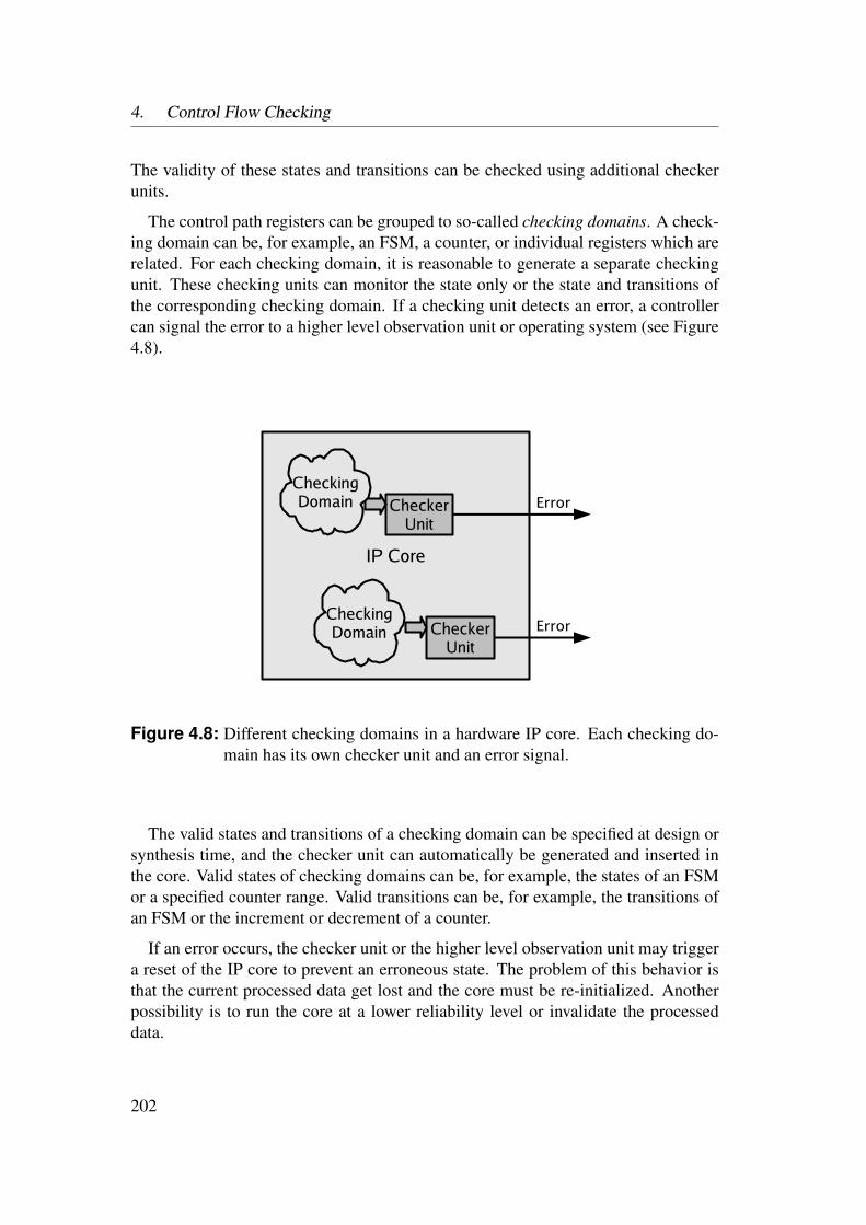
4. Control Flow Checking
The validity of these states and transitions can be checked using additional checkerunits.
The control path registers can be grouped to so-called checking domains. A check-ing domain can be, for example, an FSM, a counter, or individual registers which arerelated. For each checking domain, it is reasonable to generate a separate checkingunit. These checking units can monitor the state only or the state and transitions ofthe corresponding checking domain. If a checking unit detects an error, a controllercan signal the error to a higher level observation unit or operating system (see Figure4.8).
IP Core
CheckerUnit
CheckerUnit
Error
Error Checking
Domain
Checking Domain
Figure 4.8: Different checking domains in a hardware IP core. Each checking do-main has its own checker unit and an error signal.
The valid states and transitions of a checking domain can be specified at design orsynthesis time, and the checker unit can automatically be generated and inserted inthe core. Valid states of checking domains can be, for example, the states of an FSMor a specified counter range. Valid transitions can be, for example, the transitions ofan FSM or the increment or decrement of a counter.
If an error occurs, the checker unit or the higher level observation unit may triggera reset of the IP core to prevent an erroneous state. The problem of this behavior isthat the current processed data get lost and the core must be re-initialized. Anotherpossibility is to run the core at a lower reliability level or invalidate the processeddata.
202

4.4 Architectures for Control Flow Checking
4.4 Architectures for Control Flow Checking
In this section, we present hardware architectures to implement the control flowchecking methods described in the last section.
First, architectures for methods of checking the control flow of embedded CPUsare presented. These architectures are implemented in a module-based way so thatmethods for checking different types of instructions can be easily combined. First,in Section 4.4.1, architectures for checking direct jumps and branches as well as noncontrol flow instructions are presented. These two direct CFI checking architecturesprovide basic modules which can be extended by other checking modules or inter-faces. For indirect jumps, we provide extensions in Section 4.4.2 which use compile-time information and a return stack architecture. Techniques to handle interrupts andtraps are implemented in a further extension. Also, techniques for checking the in-tegrity of all instructions are presented. Finally, the extension to re-execute erroneousinstructions to correct a corrupt control flow is presented in Section 4.4.6. Our archi-tecture concept for checking the control flow of embedded CPUs is modular in thesense that the above coverage aspects can be traded off for implementation overhead.
Furthermore, architectures and techniques for checking general IP cores are intro-duced in Section 4.4.8, and in Section 4.4.9 and 4.4.10, a fault coverage and areaoverhead discussion of all proposed architectures and extensions are presented.
4.4.1 Handling Direct Jumps and Branches
In this section, we describe the basic architectures for the CF and CFI method intro-duced in Section 4.3.2 to check the control flow of direct jumps and branches as wellas non control flow instructions. In particular, the CFG/CFIG information is mappedto dedicated memories as it will be shown next.
To check the control flow, the checker must know the instruction’s program ad-dress PCn and the address of the next instruction PCn+1 to execute. Since most CPUarchitectures today are pipelined, these addresses can easily be taken from successivepipeline stages of the program counter.
If no jump or branch instruction occurs, the next instruction address is typicallyone instruction word higher than the value of the current program counter (PCn+1 =PCn + 1). So, an incremented instruction address can be compared to the addressafter the instruction (see comparator a in Figure 4.9 and 4.10). Otherwise, if thecurrent instruction is a direct jump or branch instruction, the next program counter isthe jump or branch destination if the branch is taken. If the branch is not taken, thenext address in the program code is the next instruction address.
In Section 4.3.2, we have shown how the correct address of direct jumps andbranches as well as the correct targets can be gathered from the program code. Here,we present the architectures for the corresponding methods.
203

4. Control Flow Checking
An Architecture for the CFI Method
Each pair of control flow instruction address and target address is stored in two mem-ories of the checker unit, one for the start and one for the target address (see Figure4.9). The addresses of the branch or jump instructions are stored subsequently in thestart address memory (sAdrRam) and the corresponding targets in the jump addressmemory (jAdrRam). Also, a checker unit program counter (CUPC) is needed whichpoints to the index of these memories where the address of the next direct branchor jump is stored. The CUPC implements the index of the next CFI described inSection 4.3.2. The start address in the START ADDR register is compared to the cur-rent program counter to determine whether a branch or jump instruction is executed(comparator b). In this case, the following program counter value is compared tothe address of the jump address RAM (TARGET ADDR register) to verify the correctexecution of the branch or the jump (comparator c). Now, the CUPC must point tothe next branch or jump address. This can be achieved by introducing a third mem-ory (ctrlRam or the suc memory in Section 4.3.2) where the next CUPC is stored foreach branch or jump. The next CUPC value is a part of the ctrlRam and thereforefor the CTRL register. After successfully checking a CFI, the values for the next CFIare loaded from all three memories into the corresponding registers: START ADDR,TARGET ADDR, and the CTRL register. By reaching the next CFI (comparator bdelivers true), the CFI can be checked without any wait cycle.
If the CFI is a branch, it must also be determined if the branch is taken or not.If the branch is taken, the next CUPC has the value which is stored in the ctrlRam.If the branch is not taken, then the CUPC is incremented. To distinguish betweenjumps and branches, we need additional memory space to store this information (seethe flags memory in Section 4.3.2). Here, we join the suc and flag memory columnsto one memory, called ctrlRam.
The CUPC and the ctrlRam present a micro-programmed architecture which im-plements the CFIG. The CUPC can be compared with the index of the CFI. Thetransitions of the CFIG are stored in the ctrlRam.
An Architecture for the CF Method
In the following, we describe an architecture for implementing the CF method intro-duced in Section 4.3.2. To check the correct execution of control flow instructions,we need the address of the currently executed instruction PCn and the addresses ofthe next instruction to execute (PCn+1). Checking the right execution sequence ofprogram counter values is done similar to the CFI method (see Section 4.4.1). Weare also using three comparators and a control RAM (ctrlRam) with a control unitprogram counter (CUPC) (see Figure 4.10).
Different from the previously proposed CFI method, however, the CF method isusing only two RAMs instead of three: the address RAM (adrRam) and the ctrl-
204

4.4 Architectures for Control Flow Checking
PCn
PCn+1
a
c
TARGETADDR
b
STARTADDR
CTRL
jAdrRamsAdrRam ctrlRam
=
=
=
+
1
+
1
CUPCflags
INDEX
Figure 4.9: Architecture for a control flow checker unit with three memories andthree comparators a, b, and c. Also, the control unit program counter(CUPC) is shown.
Ram. The end addresses of all basic blocks (BB) of the checked code sequence arestored successively in the memory adrRam. A memory for the target addresses is notneeded, because the jump and branch targets can be calculated from the values in theadrRam (see Section 4.3.2). The index (CUPC value) of the following basic block tobe executed after the currently executed basic block and some control flags are storedin the memory ctrlRam. The control flags denote the kind of the last instruction ofthe basic block. This can be either a CALL, BRANCH, RETURN, or a non controlflow instruction.
The correct address of a control flow instruction and its target address cannot eas-ily be read out of the RAMs like in the case of the CFI method. The end of thecurrent basic block is stored in adrRam[CUPC], and the correct address of the fol-lowing instruction is stored in adrRam[ctrlRam[CUPC]− 1] + 1. In contrast to theCFI method, however, we need two accesses to the adrRam in order to obtain thecorrect pair of instruction address and next instruction address at the end of a basicblock. However, the control flow check should be possible within one clock cycle tohave the ability to re-execute the instruction. To avoid a wait cycle, the correct pairof address and next address for the end of the basic block can be read when enteringthe basic block. Nevertheless, if the basic block consists of only one instruction, await cycle needs to be introduced.
205
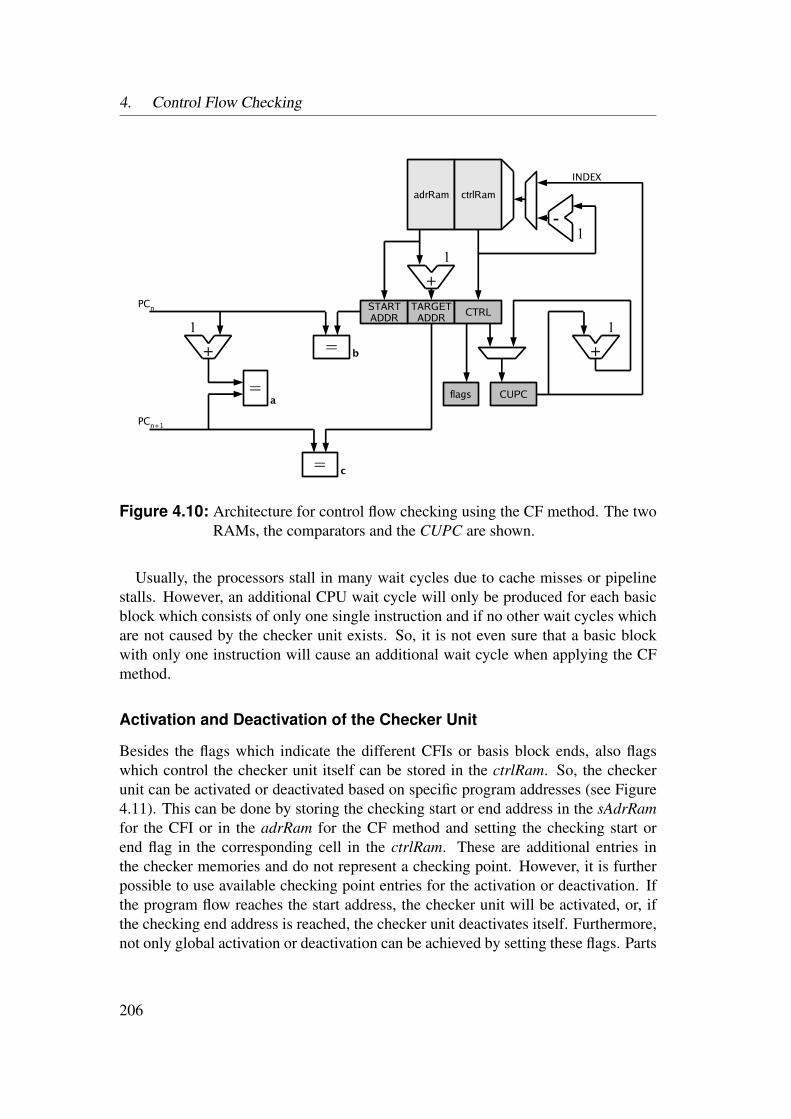
4. Control Flow Checking
PCn
PCn+1
a
c
TARGETADDR
b
STARTADDR CTRL
adrRam ctrlRam
=
=
=
+
1
+
1
CUPCflags
INDEX
+
1
-1
Figure 4.10: Architecture for control flow checking using the CF method. The twoRAMs, the comparators and the CUPC are shown.
Usually, the processors stall in many wait cycles due to cache misses or pipelinestalls. However, an additional CPU wait cycle will only be produced for each basicblock which consists of only one single instruction and if no other wait cycles whichare not caused by the checker unit exists. So, it is not even sure that a basic blockwith only one instruction will cause an additional wait cycle when applying the CFmethod.
Activation and Deactivation of the Checker Unit
Besides the flags which indicate the different CFIs or basis block ends, also flagswhich control the checker unit itself can be stored in the ctrlRam. So, the checkerunit can be activated or deactivated based on specific program addresses (see Figure4.11). This can be done by storing the checking start or end address in the sAdrRamfor the CFI or in the adrRam for the CF method and setting the checking start orend flag in the corresponding cell in the ctrlRam. These are additional entries inthe checker memories and do not represent a checking point. However, it is furtherpossible to use available checking point entries for the activation or deactivation. Ifthe program flow reaches the start address, the checker unit will be activated, or, ifthe checking end address is reached, the checker unit deactivates itself. Furthermore,not only global activation or deactivation can be achieved by setting these flags. Parts
206

4.4 Architectures for Control Flow Checking
of the program flow, e.g., non-critical sections or sections which cannot be checkeddue to not supported indirect jumps, might be excluded from the checking process bysetting the checking start and end flags.
0x0000..
0x01af....
0x02c3...
0x047c....
0x0677
checked program path
program memory
0x01af.
0x02c30x047c
.0x0677
activate.
deactivateactivate
.deactivate
unchecked program path
(s)AdrRam ctrlRam
Figure 4.11: The checker unit can be activated or deactivated on certain programaddresses. If a specified address is reached, the checker unit enablesor disables itself.
4.4.2 Handling Indirect Jumps and BranchesApproaches to extend the proposed direct checking architectures for checking indi-rect jumps are discussed in this section. First, an extension for checking indirectreturns from subroutine is presented. In the second part, architectures for checkinggeneral indirect jumps are shown.
Checking Returns from a Subroutine
The major use of indirect jumps occurs in the form of returns from a subroutine,see, e.g., Table 4.1. By executing a return from subroutine instruction, the programcounter jumps to the next address after the instruction from where the subroutinewas called. The return address is typically stored in a CPU register, so the returninstruction is a special indirect jump. Returns can be verified also in our approach byintroducing an additional hardware stack. Upon a call (direct or indirect), the returnaddress is stored in the stack. Once the return instruction is executed, the correctnessof the target address can be verified.
207

4. Control Flow Checking
To integrate the return stack extension into the basic architecture (see Figure 4.12),we need the return stack itself, and an additional comparator d. Note that the returnextension can be used for both the CFI and CF basic architecture. The addresses ofreturn instructions are stored in the sAdrRam for the CFI method, or in the adrRamfor the CF method, together with the entries for checking direct jumps and branches.An additional flag in the ctrlRam, the RETURN flag, identifies these entries as theaddresses of return instructions. The field in the jAdrRam for the CFI method, andthe field for the following CUPC (index) for both methods is left empty.
PCn
PCn+1
a
c
TARGETADDR
b
STARTADDR CTRL
jAdrRamsAdrRam ctrlRam
=
=
=
+
1
+
1
CUPC
d=returnStack
flags
INDEX
Figure 4.12: The integration of the return stack extensions to the basis architecture(in this figure the CFI architecture). Upon a call, the next instructionaddress and the next CUPC must be stored on the stack. The returnaddress can be verified by the comparator d. Furthermore, the CUPCstored in the stack must write back to the CUPC register to keep thechecker unit in sync.
Upon a call which is identified by the CALL flag, the next instruction-address andthe next CUPC value is stored in the stack. The comparator b and the RETURN flagin the CTRL register identify a return instruction. With the help of comparator d, thechecker unit can verify the back-jump to the return destination. Finally, the CUPCmust be updated to the next checking point (next CFI instruction for the CFI method,
208

4.4 Architectures for Control Flow Checking
or the next BB end for the CF method) which is stored in the stack together with thereturn target address.
With this architecture, we are able to check all returns from subroutine, even if thesubroutine is called from different locations in the program code. The depth of thestack is, however, dependent on the maximum allowed nesting of function calls. Ifthe stack overflows, the checker unit is unable to check the following program flow.
Checking General Indirect Jumps
For checking general indirect jumps, the program code can be analyzed or simulatedto detect all possible destinations of all indirect jumps (see Section 4.3.3). Thesedestinations are marked as jump-able and can be stored in an additional Ram (iJmp-Ram) inside the checker unit. Also, the addresses of all indirect jump instructionsare stored in the sAdrRam (for the CFI method) or adrRam (for the CF method).In the corresponding ctrlRam, these addresses are marked as indirect jumps with anadditional flag (see Figure 4.13).
PCn
PCn+1
STARTADDR
sAdrRam
ctrlRam
CUPC
0x17f2 indirectiJmpRam
TARG.ADDR CUPC
Search forPCn+1
found / not found
b=
Figure 4.13: If an indirect jump instruction is reached, the control checker searchesin the iJmpRam the jump destination. If the destination is found, theexecution is correct.
If the program flow reaches an indirect jump, the checker unit searches the wholeiJmpRam and compares the content with the following program counter address. Ifthe address can be found, the execution is assumed allowed, and thus correct. In theother case, the checker unit reports an error. In addition to the destination address,the next value of the CUPC must be stored in the iJmpRam to synchronize the CUPCwith the real program counter to detect the next checking point correctly. Searching
209

4. Control Flow Checking
the destination address in the iJmpRam may take more than a single clock cycle. Inthe worst case, all Ram rows must be read and compared, and for each row, oneclock cycle is needed. To speed up the search, a bisection method can be used if theaddresses in the iJmpRam are stored successively.
If the search operation takes place, the execution of the CPU must be halted toenable a fast report of the error in order to correct it if necessary. The advantage ofthis method is the flexibility in the number of different jump destinations which areonly limited by the number of rows of the memory iJmpRam. The disadvantagesare the slow execution of indirect jumps and the resulting performance impact on theCPU.
Indirect jump analysis in [CHP97] shows that the number of indirect jump des-tinations is small in most cases. So, the iJmpRam can be organized such that alldestinations of one indirect jump can be stored in one row (see Figure 4.14). A maxi-mum number of stored destinations Dmax in a row must be defined. For each jumpdestination, the corresponding CUPC value must also be stored in the iJmpRam. Ifan indirect jump has more destinations than Dmax, only Dmax destinations can be ver-ified, or an additional column in the iJmpRam is inserted, where a pointer of the rowwith the next Dmax destinations is stored. The address of the indirect jump instructionis stored in the sAdrRam or adrRam as in the first approach. Additionally to the indi-rect jump flag, the address of the row from the iJmpRam with the jump destinationsis stored in the ctrlRam. If the program flow reaches an indirect jump, the state of thenext program counter is compared with all destinations in one row of the iJmpRam.With parallel comparators, this can be done in a single clock cycle per row. If the nextstate of the program counter equals to one destination, the execution of the indirectjump is correct and CUPC is updated with the corresponding value form iJmpRam.The advantages of this method are the fast verification of the jump destinations andindividual checking for each indirect jump. The disadvantage is a larger resourceoverhead due to parallel comparators and additional memory cells.
4.4.3 Handling Interrupts and TrapsA jump may also occur in case of a trap or an interrupt. If there is an exception duringthe execution of an instruction (e.g., a division by zero), a trap is triggered. Then,a jump to a fixed or predefined address where the trap table is stored, is typicallyinduced. The different kinds of traps are distinguished in the trap table, and theright trap service routine is called. After the successful execution of the trap serviceroutine, a back-jump to the instruction following the trap is initialized. Interrupts arehandled similarly with a fixed or predefined address for the interrupt table.
It is important to note that an interrupt can occur asynchronously with respect toprogram execution. So, direct jumps to the base address for the trap and interrupttable are always allowed. Now, this base address for the trap and interrupt tablecan also be stored in the checker, and therefore, these jumps may be verified, too.
210
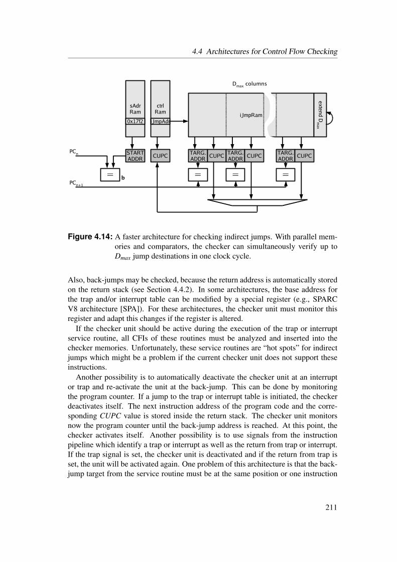
4.4 Architectures for Control Flow Checking
PCn+1
sAdrRam
ctrlRam
CUPC
0x17f2 iJmpAdriJmpRam
TARG.ADDR CUPC TARG.
ADDR CUPC TARG.ADDR CUPC
extend Dm
ax
Dmax columns
PCn STARTADDR
b= = = =
Figure 4.14: A faster architecture for checking indirect jumps. With parallel mem-ories and comparators, the checker can simultaneously verify up toDmax jump destinations in one clock cycle.
Also, back-jumps may be checked, because the return address is automatically storedon the return stack (see Section 4.4.2). In some architectures, the base address forthe trap and/or interrupt table can be modified by a special register (e.g., SPARCV8 architecture [SPA]). For these architectures, the checker unit must monitor thisregister and adapt this changes if the register is altered.
If the checker unit should be active during the execution of the trap or interruptservice routine, all CFIs of these routines must be analyzed and inserted into thechecker memories. Unfortunately, these service routines are “hot spots” for indirectjumps which might be a problem if the current checker unit does not support theseinstructions.
Another possibility is to automatically deactivate the checker unit at an interruptor trap and re-activate the unit at the back-jump. This can be done by monitoringthe program counter. If a jump to the trap or interrupt table is initiated, the checkerdeactivates itself. The next instruction address of the program code and the corre-sponding CUPC value is stored inside the return stack. The checker unit monitorsnow the program counter until the back-jump address is reached. At this point, thechecker activates itself. Another possibility is to use signals from the instructionpipeline which identify a trap or interrupt as well as the return from trap or interrupt.If the trap signal is set, the checker unit is deactivated and if the return from trap isset, the unit will be activated again. One problem of this architecture is that the back-jump target from the service routine must be at the same position or one instruction
211
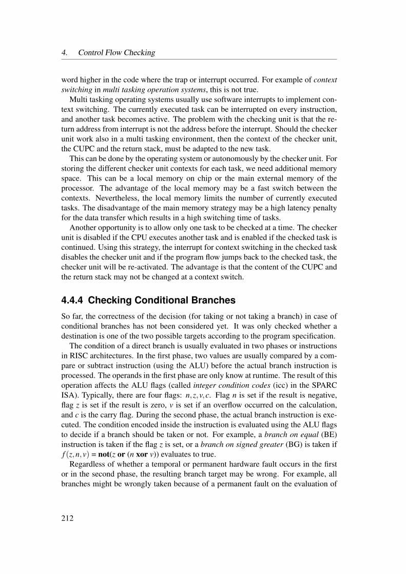
4. Control Flow Checking
word higher in the code where the trap or interrupt occurred. For example of contextswitching in multi tasking operation systems, this is not true.
Multi tasking operating systems usually use software interrupts to implement con-text switching. The currently executed task can be interrupted on every instruction,and another task becomes active. The problem with the checking unit is that the re-turn address from interrupt is not the address before the interrupt. Should the checkerunit work also in a multi tasking environment, then the context of the checker unit,the CUPC and the return stack, must be adapted to the new task.
This can be done by the operating system or autonomously by the checker unit. Forstoring the different checker unit contexts for each task, we need additional memoryspace. This can be a local memory on chip or the main external memory of theprocessor. The advantage of the local memory may be a fast switch between thecontexts. Nevertheless, the local memory limits the number of currently executedtasks. The disadvantage of the main memory strategy may be a high latency penaltyfor the data transfer which results in a high switching time of tasks.
Another opportunity is to allow only one task to be checked at a time. The checkerunit is disabled if the CPU executes another task and is enabled if the checked task iscontinued. Using this strategy, the interrupt for context switching in the checked taskdisables the checker unit and if the program flow jumps back to the checked task, thechecker unit will be re-activated. The advantage is that the content of the CUPC andthe return stack may not be changed at a context switch.
4.4.4 Checking Conditional BranchesSo far, the correctness of the decision (for taking or not taking a branch) in case ofconditional branches has not been considered yet. It was only checked whether adestination is one of the two possible targets according to the program specification.
The condition of a direct branch is usually evaluated in two phases or instructionsin RISC architectures. In the first phase, two values are usually compared by a com-pare or subtract instruction (using the ALU) before the actual branch instruction isprocessed. The operands in the first phase are only know at runtime. The result of thisoperation affects the ALU flags (called integer condition codes (icc) in the SPARCISA). Typically, there are four flags: n,z,v,c. Flag n is set if the result is negative,flag z is set if the result is zero, v is set if an overflow occurred on the calculation,and c is the carry flag. During the second phase, the actual branch instruction is exe-cuted. The condition encoded inside the instruction is evaluated using the ALU flagsto decide if a branch should be taken or not. For example, a branch on equal (BE)instruction is taken if the flag z is set, or a branch on signed greater (BG) is taken iff (z,n,v) = not(z or (n xor v)) evaluates to true.
Regardless of whether a temporal or permanent hardware fault occurs in the firstor in the second phase, the resulting branch target may be wrong. For example, allbranches might be wrongly taken because of a permanent fault on the evaluation of
212
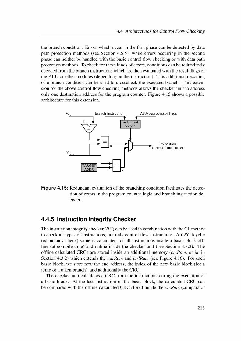
4.4 Architectures for Control Flow Checking
the branch condition. Errors which occur in the first phase can be detected by datapath protection methods (see Section 4.5.5), while errors occurring in the secondphase can neither be handled with the basic control flow checking or with data pathprotection methods. To check for these kinds of errors, conditions can be redundantlydecoded from the branch instructions which are then evaluated with the result flags ofthe ALU or other modules (depending on the instruction). This additional decodingof a branch condition can be used to crosscheck the executed branch. This exten-sion for the above control flow checking methods allows the checker unit to addressonly one destination address for the program counter. Figure 4.15 shows a possiblearchitecture for this extension.
redundantdecoder
executioncorrect / not correct
ALU/coprocessor flagsPCn
PCn+1
a=
+
1
c=TARGET
ADDR
branch instruction
Figure 4.15: Redundant evaluation of the branching condition facilitates the detec-tion of errors in the program counter logic and branch instruction de-coder.
4.4.5 Instruction Integrity Checker
The instruction integrity checker (IIC) can be used in combination with the CF methodto check all types of instructions, not only control flow instructions. A CRC (cyclicredundancy check) value is calculated for all instructions inside a basic block off-line (at compile-time) and online inside the checker unit (see Section 4.3.2). Theoffline calculated CRCs are stored inside an additional memory (crcRam, or iic inSection 4.3.2) which extends the adrRam and ctrlRam (see Figure 4.16). For eachbasic block, we store now the end address, the index of the next basic block (for ajump or a taken branch), and additionally the CRC.
The checker unit calculates a CRC from the instructions during the execution ofa basic block. At the last instruction of the basic block, the calculated CRC canbe compared with the offline calculated CRC stored inside the crcRam (comparator
213
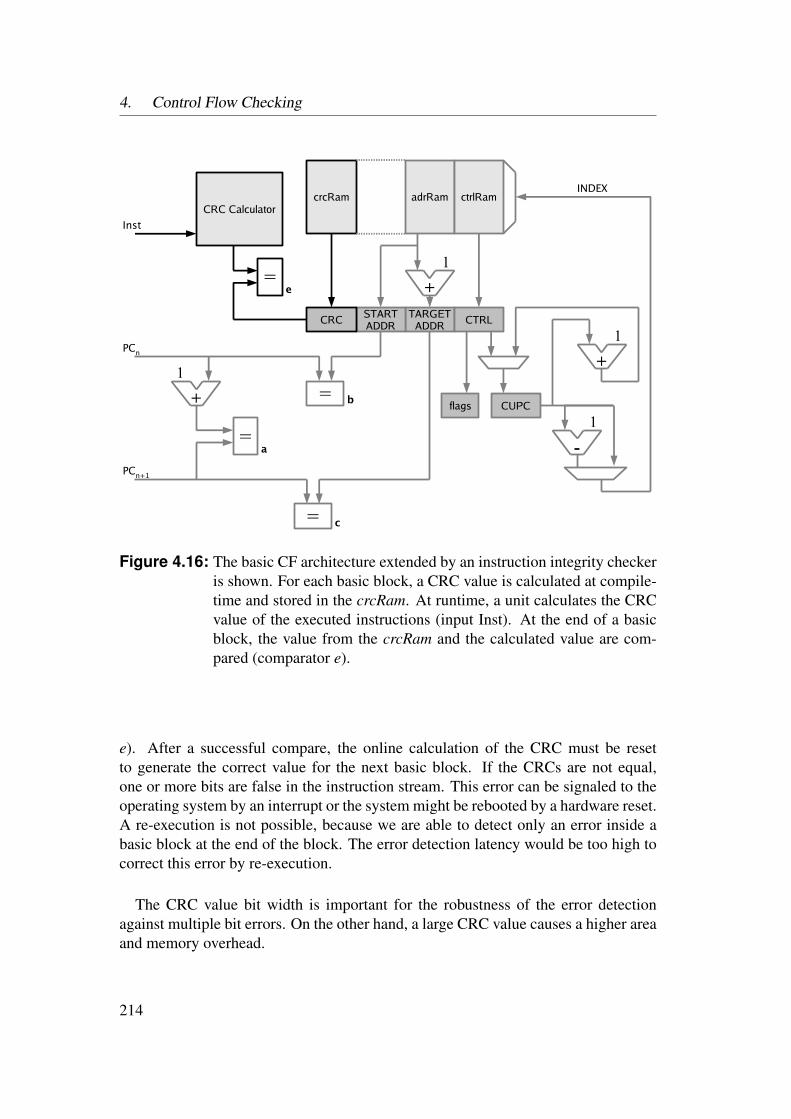
4. Control Flow Checking
PCn
PCn+1
a
c
TARGETADDR
b
STARTADDR CTRL
adrRam ctrlRam
=
=
=
+
1+
1
CUPCflags
INDEX
+
1
-
1
CRC
crcRamCRC Calculator
e=
Inst
Figure 4.16: The basic CF architecture extended by an instruction integrity checkeris shown. For each basic block, a CRC value is calculated at compile-time and stored in the crcRam. At runtime, a unit calculates the CRCvalue of the executed instructions (input Inst). At the end of a basicblock, the value from the crcRam and the calculated value are com-pared (comparator e).
e). After a successful compare, the online calculation of the CRC must be resetto generate the correct value for the next basic block. If the CRCs are not equal,one or more bits are false in the instruction stream. This error can be signaled to theoperating system by an interrupt or the system might be rebooted by a hardware reset.A re-execution is not possible, because we are able to detect only an error inside abasic block at the end of the block. The error detection latency would be too high tocorrect this error by re-execution.
The CRC value bit width is important for the robustness of the error detectionagainst multiple bit errors. On the other hand, a large CRC value causes a higher areaand memory overhead.
214

4.4 Architectures for Control Flow Checking
4.4.6 Repairing a Corrupt Control Flow by Re-Execution
If an erroneous control flow caused by a corrupt instruction is detected, the corre-sponding instruction must be annulled and re-executed. The problem is that the en-trance of the erroneous instruction in the processor pipeline and the observable effectof the corrupted control flow do not happen at the same time. In fact, many clockcycles can elapse between both events. Furthermore, due to faults in the proces-sor pipeline, the instruction might become erroneous inside the pipeline after it wasfetched from the memory. In both cases, many other instructions could enter theprocessor pipeline after the corrupted instruction.
The first step after the detection of the erroneous control flow is to stall the respon-sible instruction and all following instructions in the pipeline at the correspondingpipeline stages. Many processor architectures support an annul flag which preventsthe corresponding instructions from execution. This flag can be used for the erro-neous as well as the following instruction in the pipeline. This should be done fastenough to prevent the erroneous control flow to alter the state of the processor, e.g,write registers, or initiate memory write accesses. Fortunately, these actions happenusually at the last pipeline stage. Therefore, the detection of the corrupted controlflow should be as fast as possible which results that the checker unit should monitorthe control flow on the first pipeline stage.
The second step is to insert the address of the corrupted instruction at the firstpipeline stage which results in a re-fetch and re-execution of the instruction. Toidentify the responsible instruction and the corresponding instruction address, theinformation of the stored graph inside the checker memories can be used.
The example program in Figure 4.17 demonstrates the proposed re-execution tech-nique. On the left side, let the branch instruction at address 0x4d be responsible fora wrong branch target (0xde). The checker unit cannot recognize this error beforethe corrupt instruction reaches the third pipeline stage. Therefore, the branch and thefollowing two instructions are annulled by setting a corresponding annul flag A andthe branch instruction address is forwarded to the pipeline by the checker unit to fetchthe branch instruction again. During the second try shown on the right side, let thebranch be executed correctly. Furthermore, the previously annulled instructions havenow moved to later pipeline stages, but the annul bit prevents these instructions fromexecution.
To support this re-execution technique by the basic checker architectures, we needtwo additional outputs of the checker unit. The first one is the instruction address(CPCREEXPC) from where the re-execution should start. The second output (CPC-REEXCODE) tells the processor pipeline how many instructions should be annulled.The CPCREEXPC signal is derived from the STARTADDR register, if the the erro-neous instruction is an CFI. If not, the signal is taken from a history register, whichstores the program counter value of the previous cycle (see Figure 4.18). The numberof annulled instructions (CPCREEXCODE) can be derived from the checker flags
215
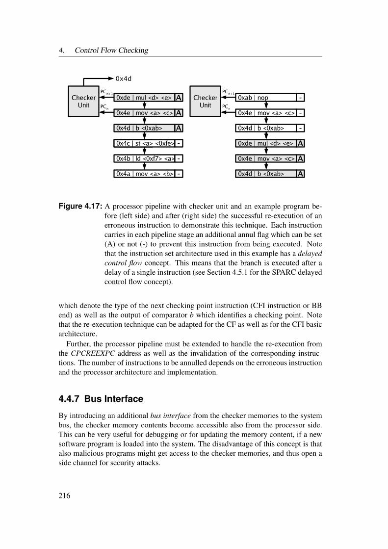
4. Control Flow Checking
0xde | mul <d> <e>
0x4d | b <0xab>
Memory Inst
0x4e | mov <a> <c>
0x4b | ld <0xf7> <a>
0x4a | mov <a> <b>
0x4c | st <a> <0xfe>
CheckerUnit
PCn+1
PCn
A
A
A
-
-
-
0x4d
0xde | mul <d> <e>
0x4d | b <0xab>
0x4e | mov <a> <c>
0x4e | mov <a> <c>
0x4d | b <0xab>
0xab | nopCheckerUnit
PCn+1
PCn
A
A
A
-
-
-
Figure 4.17: A processor pipeline with checker unit and an example program be-fore (left side) and after (right side) the successful re-execution of anerroneous instruction to demonstrate this technique. Each instructioncarries in each pipeline stage an additional annul flag which can be set(A) or not (-) to prevent this instruction from being executed. Notethat the instruction set architecture used in this example has a delayedcontrol flow concept. This means that the branch is executed after adelay of a single instruction (see Section 4.5.1 for the SPARC delayedcontrol flow concept).
which denote the type of the next checking point instruction (CFI instruction or BBend) as well as the output of comparator b which identifies a checking point. Notethat the re-execution technique can be adapted for the CF as well as for the CFI basicarchitecture.
Further, the processor pipeline must be extended to handle the re-execution fromthe CPCREEXPC address as well as the invalidation of the corresponding instruc-tions. The number of instructions to be annulled depends on the erroneous instructionand the processor architecture and implementation.
4.4.7 Bus Interface
By introducing an additional bus interface from the checker memories to the systembus, the checker memory contents become accessible also from the processor side.This can be very useful for debugging or for updating the memory content, if a newsoftware program is loaded into the system. The disadvantage of this concept is thatalso malicious programs might get access to the checker memories, and thus open aside channel for security attacks.
216

4.4 Architectures for Control Flow Checking
PCn
PCn+1
a
c
TARGETADDR
b
STARTADDR
CTRL
jAdrRamsAdrRam ctrlRam
=
=
=
+
1
+
1
CUPCflags
INDEX
+
1
histPC
CPCREEXCODE
CPCREEXPC
Figure 4.18: The basic CFI architecture with the re-execution extension. The twoadditional outputs (CPCREXPC and CPCREEXCODE) are shown.Note, the re-execution extensions work also with the CF basis archi-tecture as well as with the return stack extension.
Another fact is that internal on-chip memory is very expensive (see Section 1.2.6).If the checker unit has a bus interface, the contents or part of the content of thechecker memory may also be stored in the external system memory. Only the con-tent for checking the current part of the program (e.g., the current function or aset of functions which are currently in use) may therefore be held in the internalchecker memories. If the checker needs information which is not stored inside thelocal checker memories, the checker can generate a page-fault-like event to reloadthe checker memories with the needed contents. This concept of caching may reducethe amount of internal memory overhead significantly.
To have access to an existing system memory, the checker memories need a businterface. The architecture and implementation of the bus interface depends highlyon the used bus protocol.
217

4. Control Flow Checking
4.4.8 IP Core Control Flow Checking
In Section 4.3.5, possibilities for identifying control path registers in general IP coresare shown. In this section, we concentrate on checking finite state machines (FSMs)in general and counters in control paths when specified by FSMs.
An FSM is defined as a 6-tuple (ΣM,ΓM,SM,s0M,δM,ωM), where ΣM is the inputalphabet, ΓM is the output alphabet, SM is a finite set of states, s0M is the initial state,δM is the state-transition function, and ωM is the output function. The internal stateqM ∈ SM is stored in a state register. The transitions between the states are controlledby the state-transition function δM : SM×ΣM → SM which uses the current state qMand the current inputs xM ∈ ΣM into the FSM to calculate the next state δ (qM,xM).This function is implemented using combinatorial logic. If a Moore model is used, theoutputs ΓM depend only on the states: ωM : SM→ ΓM. Whereas the output of a Mealymachine depends on the states and the inputs: ωM : SM × ΣM → ΓM. Faults (e.g.,SEU, SET) inside an FSM can lead to an erroneous state or to erroneous transitionsbetween the states. The general IP core checking methods can check if a state qM isvalid, i.e., qM ∈ SM. Furthermore, it checks for a given next state qMn if this state isvalid according to δM, i.e., ∃xM ∈ ΣM : δM(qMn−1,xM) = qMn. It does not check thecondition and the timing depending on the inputs xM when a state is entered or left.
A counter is a specific FSM, more precisely the implementation of a specific Mooreautomaton. The state qM is given uniquely by the counter value. The states aresequentially ordered in a chain, which can be traversed in any direction. Here, wecan also check the states (the counter range) and the transitions between the states(counting up/down).
Checking the State
An FSM has a finite number of states qM ∈ SM. These states are encoded in a specifiedmanner into a state vector, which can be implemented and stored by a register. Thereexist many different encodings, e.g., gray, sequential, or 1-hot coding. Depending onthe encoding, and the available bits for the state register, the number of presentablestates can be higher than the actually used states. This means that not all possiblestates which can be represented by an n-bit register are valid.
To check if a state encoded into a register value is valid, we can use a combinatoriallogic which has the state register qM as input and an error signal as output. If thestate is valid, i.e., qM ∈ SM, the output is ’0’, otherwise ’1’. A straight forwardimplementation of this logic is a lookup table, where all invalid states are markedwith a ’1’ as output. One problem with this technique is that an erroneous transitionfrom one valid state to an other valid state is not detected. If the state vector has anormal binary encoding, the number of invalid state encoding is low which may leadto many undetected erroneous transitions.
218
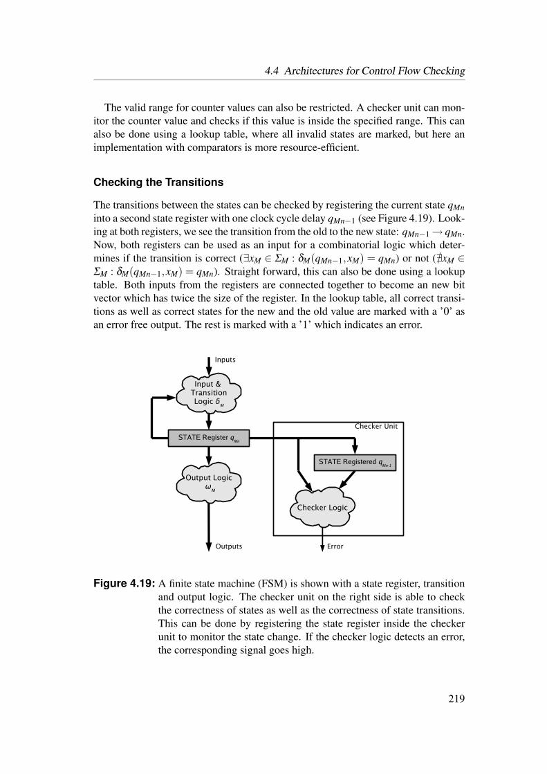
4.4 Architectures for Control Flow Checking
The valid range for counter values can also be restricted. A checker unit can mon-itor the counter value and checks if this value is inside the specified range. This canalso be done using a lookup table, where all invalid states are marked, but here animplementation with comparators is more resource-efficient.
Checking the Transitions
The transitions between the states can be checked by registering the current state qMninto a second state register with one clock cycle delay qMn−1 (see Figure 4.19). Look-ing at both registers, we see the transition from the old to the new state: qMn−1→ qMn.Now, both registers can be used as an input for a combinatorial logic which deter-mines if the transition is correct (∃xM ∈ ΣM : δM(qMn−1,xM) = qMn) or not (@xM ∈ΣM : δM(qMn−1,xM) = qMn). Straight forward, this can also be done using a lookuptable. Both inputs from the registers are connected together to become an new bitvector which has twice the size of the register. In the lookup table, all correct transi-tions as well as correct states for the new and the old value are marked with a ’0’ asan error free output. The rest is marked with a ’1’ which indicates an error.
STATE Register qMn
Error
STATE Registered qMn-1
Input & TransitionLogic δ
M
Output Logic ω
M
Checker Logic
Outputs
Inputs
Checker Unit
Figure 4.19: A finite state machine (FSM) is shown with a state register, transitionand output logic. The checker unit on the right side is able to checkthe correctness of states as well as the correctness of state transitions.This can be done by registering the state register inside the checkerunit to monitor the state change. If the checker logic detects an error,the corresponding signal goes high.
219

4. Control Flow Checking
For checking the transitions of counters, the same technique can be used. How-ever, we can see here that a lookup table implementation is very resource consuming.Implementing this function with a redundant counter saves more resources.
Implementation Issues
Implementing the checker logic with unoptimized lookup tables requires a very largeresource overhead for larger state register width. For an n-bit state register, the max-imal number of lookup table entries nE for checking only the correct state is:
nE = 2n (4.2)
For checking the correct states and the transitions the maximal number of requiredlookup table entries is:
nE = 22n (4.3)
For checking an 8-bit state register, we thus require at least 256 lookup table entries(1-bit correct/not correct) for checking the state and 65536 entries for checking thestates and the transitions for correctness. This overhead is quite huge. But dependingon the number of available used states there is also a large optimization potential. Ifwe look at a 1-hot encoding, we can check the state if we add all bits from the stateregister together and check if the result is one. This can be done for the 8-bit stateregister with a extremely low overhead than with a lookup table with 256 entries.Furthermore, the number of valid transitions is usually very low in contrast to allpossible (valid + invalid) transitions. This has also a high optimization potentialto bring the resource overhead down. Fortunately, synthesis tools are excellentlysuitable for optimizing this combinatorial problem.
One problem of the implementation is that the added checker unit represents re-dundant logic according to the synthesis tools which is usually removed due to areaoptimization. Also, the kind of state encoding as well as the proper encoding of eachstate of the FSM is usually decided by the synthesis tool. To handle these problems,the checker logic and the functional IP core shall be synthesized separately.
First, the IP core is synthesized without checker units. The different control pathsof the IP core which should be checked can now be chosen and the correspondingstate encoding scheme as well as the proper state coding can be taken from the syn-thesis report. Furthermore, a specification of the correct state transitions for the FSMsand/or the valid range for counters as well as the counter type (up, down, up/down)for generation of the checker unit is needed. For each checked control path a separatechecker unit is instantiated. These checker units can now be optimized and translatedinto a netlist by a synthesis tool. Finally, in the IP core netlist, we must insert blackbox instances which ingest later the checker units and connect the state or counter
220

4.4 Architectures for Control Flow Checking
register to these black boxes as well as the error signal to an IP core output. The IPcore and the checker units will be integrated in the following implementation steps.
In summary, this method and architecture can check the state and the state transi-tions of FSMs and counters embedded in general IP cores. Only errors which resultin an erroneous state or take an erroneous transition can be detected. The robustnessof an FSM can be increased by using a state encoding, e.g., 1-hot encoding, whereerrors lead to an erroneous state in most cases. The overhead depends on the registerbit width as well as on the encoding type. By using different checking domains withdifferent configurations (only checking states or states and transitions), checking thecontrol paths in hardware IPs is modular and widely parametrical. Furthermore, adesign flow to implement these methods was shown.
4.4.9 Fault Coverage
In the previous sections, the building blocks of an architecture which is able to checkand correct the control flow of CPU programs for RISC processors were introduced.The cadre of this architecture is based on one of the two alternative basic modules forthe CF and CFI method (see Section 4.4.1). These methods can be extended by thereturn stack and/or the other indirect checking architectures shown in Section 4.4.2 toalso support the checking of indirect jumps as well as methods to support and checkinterrupts and traps (see Section 4.4.3).
Obviously, which different types of faults can be detected depends heavily on theproposed error detection method. Fault coverage refers to the percentage of faultswhich can be detected from a defined set of faults. With the instruction integritychecker (see Section 4.4.5) and the conditional branch checker extensions (see Sec-tion 4.4.4), we are able to detect more errors and faults than using the basic methods.Finally, the re-execution extension (see Section 4.4.6) gives us the possibility to cor-rect errors which lead, if uncorrected, to an erroneous control flow.
The basic architecture of the CFI and CF method described in Section 4.4.1 is ableto detect the following types of faults:
• All permanent and transient faults in instruction memory, memory bus, mem-ory controller, instruction cache instruction register, and logic between differ-ent pipelined instruction registers, if the instruction affects the control flow.
• All permanent and transient faults which lead to errors in the program counterregister, the logic between different pipelined program counter registers as wellas the logic of the calculation of the next program counter.
• Security flaws which affect the control flow (e.g., stack and heap smashingattacks) with the return stack extension.
221
4. Control Flow Checking
• Design faults in hardware which can be detected through diversity of the pro-cessor core and the checker unit, and in software caused by diversity betweenthe compiled program and the checker unit entries (e.g., unauthorized softwareupdate).
Using the CF-method with the additional instruction integrity checker extensionpresented in Section 4.4.5, we can further detect the following types of faults besidesthose mentioned above:
• All permanent and transient faults leading to errors in the instruction mem-ory, memory bus, memory controller, instruction cache instruction register, andlogic between different pipelined instruction registers which appear before thepipeline step where the instruction integrity checker is instantiated.
Furthermore, using the conditional branch checker extensions (see Section 4.4.4),we are able to detect the following faults besides the previously mentioned faultsabove:
• All permanent and transient faults which lead to a false decoding of branchinstructions which results in an erroneous decision of taking or not taking abranch.
The general IP checker method is able to detect faults in FSMs and counters whichlead to invalid states or to erroneous, unspecified transitions. Note that the timingbehavior of the transition and the conditions are not checked.
4.4.10 Overhead Discussion
To evaluate the control flow checking architectures, it is necessary to consider therequired overhead. In this section, mainly the area and execution time overheads arein focus. The memory overhead for the different basic architectures were already dis-cussed in Section 4.4.1. To have a technology independent area overhead discussion,we decided to use primitive components (see Section 1.2.6) to describe the overhead.
Overhead of the Basic Architectures
The overhead in terms of primitive components of the basis architecture of the CFImethod (see Section 4.4.1) is:
• 1×30-bit adder,
• 1×ncupc-bit adder,
• 3×30-bit comparator,
222
4.4 Architectures for Control Flow Checking
• 11 flip-flops,
where ncupc denotes to the CUPC width.Additionally, three block memories and some resources for the control logic which
cannot be measured in terms of primitive components are required. Also, the bitwidth of the adders and the flip-flops can alter slightly due to different memory sizes.An important hint of complexity is the number of checker memory entries which isdependent on the index and therefore the CUPC width (ncupc) to address the memo-ries. Furthermore, the CUPC width also has impact on the word width of the ctrlRam.The number of necessary checker memory entries depends on the checked programand the number of checked functions. For both methods, the number of necessarychecker entries for the SPEC CINT2000 benchmark programs, if all functions arechecked, is shown in Table 4.2 in Section 4.3.2.
The area overhead of the basic architecture using the CF method (see Section 4.4.1)is very similar to the values above. However, due to more complex control logic (twoaccesses to the RAM), the area overhead of the CF method is always higher than theoverhead of the CFI method.
The resource requirements in terms of primitive components of the CF method are:
• 2×30-bit adder,
• 2×ncupc-bit adder,
• 3×30-bit comparators,
• 44 flip-flops.
Additionally, two local memories and additional resources for the control logicare required. Alike the CFI method, the bit width of the adders and the number offlip-flops can vary slightly due to different memory sizes.
The memory overhead of the CF method has already been discussed in Section4.3.2. In summary, the CF method usually requires fewer memory resources for thesame program than the CFI method.
If the program code contains basic blocks consisting of only one instruction, theremight be an extra CPU time penalty. Usually, the processors stall in many wait cyclesdue to cache misses or pipeline stalls. However, an additional CPU wait cycle willonly be produced for a basic block which consists of only one instruction and if noother wait cycles exist, which are not caused by the checker unit. Hence, it is not evensure that a basic block with only one instruction will actually cause an additional waitcycle if the CF method is used.
We have introduced several extensions for both basic methods of control flowchecking. The overhead of these extensions is discussed next.
223

4. Control Flow Checking
Overhead of the Return Stack
Returns from subroutine can be verified by introducing an additional hardware stack.Upon a call (direct or indirect), the return address may be stored on the stack. Whenthe return instruction is executed, the target address can be verified.
The caused memory overhead depends on the depth of the stack. To store an in-struction address, we need 30-bits for a 32-bit processor. The last 2 bits address theindividual bytes inside an instruction and do not need to be stored on the stack. Ad-ditionally, we must store the corresponding CUPC value to denote the next checkingpoint in case of a return instruction. Using a 32-bit processor, the memory overheadis therefore (30 bit+ncupc)×dstack, where dstack is the stack depth.
Also, the return stack causes additional area overhead for control logic which de-pends on the implementation.
Overhead of Indirect Jump Extensions
The memory overhead of the extensions for checking indirect jumps as introduced inSection 4.4.2 depends on the number of the indirect jump memory (iJmpRam) entriesand the width of the CUPC (checker unit program counter) register ncupc. For eachindirect jump which we would like to check in the code, we need one memory row inboth methods. The total memory overhead for the first method for a 32-bit processoris therefore in bits:
(30 bit +ncupc)×nT (4.4)
where nT denotes to the number of all indirect jump targets.For the second method in Section 4.4.2, the total memory overhead in bits is:
((30 bit +ncupc)×Dmax +ncupc)×niJ (4.5)
where niJ denotes to the number of all indirect jumps.The area overhead in terms of primitive components for the first method is there-
fore:
• min. 1×30-bit comparator and• logic for searching the indirect jump (e.g., bisection method).
The area overhead for the second method is:
• Dmax×30-bit comparators,• 1×ncupc-bit Dmax to 1 multiplexer, and
224
4.4 Architectures for Control Flow Checking
• control logic.
The execution time overhead for the first methods depends on the search algorithm.Using a bisection method, we need n+1 clock cycles for searching an indirect jumptarget among 2n entries. During this time, the processor must be stalled if we want tohave the possibility to re-execute an indirect jump if an error has occurred.
In the second method, we are able to check Dmax targets during one single clockcycle. If the indirect jump has more then Dmax possible targets, we produce an ex-ecution time overhead. The overhead in terms of clock cycles can be determinedas
⌊ nt
Dmax
⌋, (4.6)
where nt is the number of possible targets of an indirect jump.
Overhead of the Interrupt and Trap Extension
The interrupt and trap extension (see Section 4.4.3) enhances the basic method tosupport interrupts and traps. The easiest way is to evaluate signals from the processorpipeline which indicate if an interrupt or a trap occurs or if the interrupt or trapsservice routine is left to continue the execution of the checked function (return frominterrupt or trap). In this case, we only need some additional control logic to evaluatethese signals to deactivate or activate the checker unit.
If also the jump to and from the service routine should be checked, we need aregister where the address of the service routine is stored. Also a comparator isneeded which identifies if a trap occurs. The back-jump can be verified using thereturn stack. Here, the trap signaling from the processor pipeline is not obligatory,but both techniques can be combined. The additional area overhead is therefore:
• 1×30-bit register,
• 1×30-bit comparator,
• control logic.
If the checker unit should check more than one thread in a multi threading op-eration system, we need additional memory to store the context of the checker unitfor each thread. This memory space can be on the external memory or on chip lo-cal memory. For each thread, the context of the checker unit consists of the currentCUPC, the current program counter, and the whole return stack.
225
4. Control Flow Checking
Overhead of Checking Conditional Branch Extension
The area overhead of checking the conditional of direct branch instructions (see Sec-tion 4.4.4) consists of the redundant instruction decoder and a one bit multiplexer(see Figure 4.15 in Section 4.4.4). The overhead of the decoder depends highly onthe used processor architecture and implementation.
Overhead of the Instruction Integrity Checker
The overhead of the instruction integrity checker extension (see Section 4.4.5) de-pends mainly on the bit width of the used CRC values. The CRC width is importantfor the robustness of the error detection against multiple bit errors. On the other hand,a large CRC value causes a higher area and memory overhead.
The area overhead in terms of primitive components is:
• 1×ncrc comparator and
• ncrc flip-flops.
Additionally, block ram and some logic for calculating the CRC and control logicis needed. The memory overhead evaluates to:
ncrc×2ncupc (4.7)
This checker unit enhancement causes no further CPU time overhead.
Overhead of the Re-Execution Extension
With the re-execution extension (see Section 4.4.6), we are able to correct a corruptcontrol flow. To re-execute an erroneous instruction, we need the start point of re-execution (CPCREEXPC) as well as the number of instructions (CPCREXCODE)which must be annulled to prevent them from execution. The area overhead in termsof primitive components inside the checker unit to calculate both values is:
• 1×30-bit adder (increment),
• 1×30-bit register (hist register),
• 1×30-bit 2 to 1 multiplexer, and
• control logic.
Furthermore, we need some additional logic in the processor pipeline to start there-execution from the CPCREEXPC and also to annul the erroneous instruction aswell as their following instructions.
226

4.4 Architectures for Control Flow Checking
Summarized Overhead Functions for Embedded Processor ControlFlow Checking
In this section, all overhead functions of the introduced control flow checking ar-chitectures are summarized in one table (see Table 4.3). Here, ncupc denotes theCUPC bit width. The CFI method can handle 2ncupc control flow instructions andthe CF method can handle 2ncupc basic blocks. dstack denotes the return stack depth,nT denotes the number of different targets for all indirect jumps, Dmax is number ofdifferent targets for one indirect jump for the indirect jump method 2 which can bechecked within one clock cycle, niJ denotes to the number of all indirect jumps, ntis the number of possible targets of an indirect jump, and finally ncrc is the CRC bitwidth. However, in Table 4.3 the overhead for control and other logic is omitted.
Area Overhead Memory CPU timeOverhead Overhead
Architecture adders compara- flip- multi- bits cyclestors flops plexers
CFI Method1×30-bit, 3×30-bit 5+ncupc
(65+ncupc) none1×ncupc-bit ×2ncupc
CF Method2×30-bit, 3×30-bit 5+ncupc (35+ncupc) none2×ncupc-bit +30 ×2ncupc
Return (30+ncupc) noneStack ×dstack
Ind. Jump min. (30+ncupc) n+1 forMethod 1 1×30-bit ×nT 2n entries
Ind. JumpMethod 2
Dmax×30-bit
1× ((30+ncupc)× ⌊nt
Dmax
⌋ncupc-bit Dmax +ncupc)Dmax to 1 ×niJ
Interrupt/ 1×30-bit 1×30 none noneTraps
Conditional 1×2 to 1 none noneBranch Ch.
Inst. Integrity 1×ncrc ncrc×2ncupc none
Checker ncrc-bitRe-Execution 1×30-bit 1×30 1×30-bit none dependsArchitecture 2 to 1 on proc.
Table 4.3: Comparison of different overheads for each control flow checkingmethod and its extensions for a 32-bit RISC processor.
In summary, CFI and CF are two alternative methods and the presented extensionscan be combined with these methods and further extensions, resulting in a modu-lar framework for control flow checking. One exception is the instruction integritychecker which can only be combined with the CF method.
227

4. Control Flow Checking
4.5 Prototypical Implementation
In this section, the proposed control flow checker architectures for embedded pro-cessors are integrated into a given Leon3 processor system from Gaisler Research[Gaib] using the SPARC V8 [SPA] instruction set. The two basic architectures forcontrol flow checking (CFI and CF architecture) with the return stack, interrupt andtrap handling, and the re-execution extension are implemented on an FPGA proto-type.
First, the control flow instructions of the SPARC V8 instruction set are presentedand some mannerism of the SPARC architecture are shown. Next, an overview of theLeon3 processor system is given. After the presentation of the processor platform, theintegration of the control flow architectures and their extensions is shown. To analyzethe compiled program code, we need an analyzer tool which generates the properentries for the checker memories. In the next section, the integration and interactionwith the data path protection technique developed by the project partner TU Munich(TUM) [BZS+06] is shown. Finally, for better understanding, some examples andexperimental results from the simulation and implementation on an FPGA prototypeare given.
4.5.1 The SPARC V8 Instruction Set Architecture
The SPARC (Scalable Processor Architecture) V8 is a 32-bit RISC (Reduced Instruc-tion Set Complexity) instruction set architecture (ISA). Like other 32-bit RISC ISAs,each of the 72 different basic instructions are encoded in a single 32-bit word whichmeans that all instructions have the same word length. The SPARC V8 architec-ture consists of an integer unit (IU) and an optional floating point unit (FPU) or aco-processor (CP). The FPU and CP have their own registers and are accessed byspecial floating point and co-processor instructions. Beside the 32-bit SPARC V8ISA, also the 64-bit SPARC V9 ISA exists.
Instruction Overview
The instructions of the SPARC V8 ISA are encoded in 32-bit words. The format ofeach 32-bit word is depending on the type of instruction. In general, there are sixdifferent categories of instructions:
• Data Transfer (Load/Store): These instructions are able to access the mem-ory. 16-bit, 32-bit, and 64-bit accesses are supported.
• Arithmetic/Logical/Shift: These instructions initiate an arithmetic, logical orshift operation.
228

4.5 Prototypical Implementation
• Control Flow: All instructions which affect the control flow. This category isdescribed in detail later.
• Read/Write Control Register: Using these instructions, special control regis-ters can be accessed.
• Floating Point Operate: This kind of instructions initiate a floating point op-eration, if a FPU is present. If not, a trap is generated, which gives the programor operating system the possibility to emulate floating point instructions in soft-ware.
• Co-Processor Operate: These instructions initiate a co-processor operation.
For a detailed description of each type of instruction, see the SPARC V8 manual[SPA].
Control Flow Instructions
The SPARC ISA consists of control flow instructions for direct jump and branchesas well as indirect jumps. The target addresses of direct branches and jumps arecalculated in a relative manner, i.e., a value which is stored inside the instruction isadded to the current program counter in order to calculate the target address. Thetargets of the indirect jumps are register indirect, which means that the target is theprogram counter added with the result of an operation of two register values, or anoperation with a register and a constant value.
The SPARC ISA uses a delayed control flow concept for almost all control flowinstructions (except conditional traps). This means that the instruction following di-rectly a control flow instruction is executed, and then, the control flow transfer isinitiated. The effect of the control flow instruction is therefore delayed by one in-struction. The instruction after a CFI is called delay instruction. Furthermore, allCFIs which use this delayed concept have a flag (annul flag or a) encoded into theinstruction which indicates if the delay instruction should be executed or not. If theannul bit is not set (a = 0), the delayed instruction is executed. Whereas, if the an-nul bit is set (a = 1), the delay instruction is prevented from execution. This has thesame effect as executing a non operation instruction (NOP). However, if the CFI is aconditional branch and the branch is taken, the delay instruction is always executed,independent of the annul flag. Figure 4.20 shows an example of this delayed controlflow concept.
The different types of control flow instructions of the SPARC V8 architecture aredescribed in the following:
Call and Link (CALL) The call and link instruction is a direct jump to an addresswhich is encoded inside the instruction relatively to the current program counter.
229

4. Control Flow Checking
MOV <r6> <r4> CALL <0x5a> a=0 ADD <r4> <r5> ... MOV <r5> <r3>
0x400x440x48...0x5a
0x40
0x44
0x48
0x5a
Figure 4.20: On the left side, a program memory snippet with a call instruction(CALL) where the annul flag is not set (a = 0) is depicted. If thisprogram code is executed (right side), the delayed instruction ADDafter the call CFI is executed before the control flow is transferred tothe call target on address 0x5a.
The instruction has no annul flag, so that the following delay instruction is alwaysexecuted. Furthermore, the current program counter is copied into a special register(r[15]). This instruction is usually used to call a subroutine.
Jump and Link (JMPL) The jump and link instruction is the common indirectjump instruction for the SPARC architecture. This unconditional jump exists in twoversions. In the first version, the target address is calculated by an addition of tworegister values. The addresses of the registers are part of the instruction. In thesecond version, the target address is calculated by an addition of a register valueand a constant value, stored inside the instruction. The current program counter isstored in a register which can be selected by the instruction. Register indirect callsand returns from subroutine are in fact also special jump and link instructions. Forexample, the RET (return from subroutine) and RETL (return from leaf subroutine)assembler instructions are only aliases for special JMPL instructions.
Branch on Integer Condition Codes (Bicc) The branch on integer conditioncodes instruction family consists of different branch instructions with different con-ditions which evaluate the integer condition codes (icc). The icc is a special registerwhich is updated by an arithmetic operation. There exist four different icc flags: n isset if the result is negative; z is set if the result is zero; v is set if there was an overflowat the operation; c is set if the carry bit is set. The condition encoded in the branch in-struction evaluates these bits and decides if the branch is taken or not. Some exampleBicc instructions are: BE (branch on equal), BG (branch on greater), BLEU (branchon less or equal unsigned). There exist also two unconditional branch instructions:BA (branch always) and BN (branch never). If the branch is taken, first the delayedinstruction is executed, and then the control flow is transferred to a target addresswhich is stored inside the instruction relatively to the current program counter. TheBicc instructions have further an annul (a) bit, which only has effect if the branch is
230

4.5 Prototypical Implementation
not taken. One exception, however, is the BA instruction which also evaluates thisbit to decide if the delay instruction is executed or not.
Branch on Floating Point Condition Codes (FBfcc) The branch on floatingpoint condition codes instruction family is very similar to the Bicc instructions. Thedifference is that the floating point condition codes are evaluated instead of the inte-ger condition codes. The floating point condition codes result from a floating pointoperation.
Branch on Co-Processor Condition Codes (CBccc) Like the FBfcc in-structions, these instructions are very similar to the Bicc instructions. Here, the co-processor condition codes are evaluated.
Trap on Integer Condition Codes (Ticc) The trap on integer condition codesinstruction can be used for programmed traps. Like the Bicc instruction, the integercondition codes are evaluated with the conditions programmed inside the instruction.Depending of this evaluation, a trap is generated or not. The conditions are the sameas for the Bicc instructions. The target of this CFI is one of the 128 software traproutines. Which trap routine is called depends either on the addition of two registervalues or on an addition of one register value with a constant which is included in theinstruction. More about traps is discussed later in this section. The Ticc instructiontransfers the control flow immediately without executing a delay instruction. Like thecall instruction, the current program counter is stored in a register, if the trap is taken.
Return from Trap (RETT) The return from trap instruction is an indirect jumpwhich is used for the back-jump from the trap routine to the instruction where thetrap has occurred. The format and behavior of this instruction is very similar to theJMPL instruction. However, this instruction further leaves the supervisor mode andenables traps.
Registers
In the SPARC V8 ISA, general purpose and control and status registers are available.All registers have a word length of 32-bit. The general purpose registers, denotedr, consist of 8 global registers and a register window consisting of 24 registers. Theglobal registers are always available, whereas the register window is dynamic.
The register window is divided into three groups: 8 in registers, 8 local registers,and 8 out registers. The register window is only a visible part of a greater registerfile. With special instructions, the register window can be shifted, so that anotherpart of the register file is visible. With the SAVE instruction, the window is shifted16 registers to the right, whereas on a RESTORE instruction, the window is shifted
231
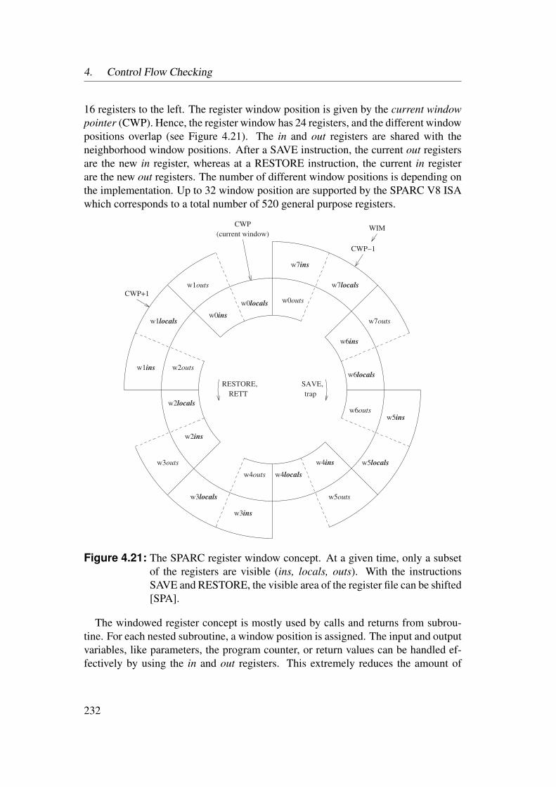
4. Control Flow Checking
16 registers to the left. The register window position is given by the current windowpointer (CWP). Hence, the register window has 24 registers, and the different windowpositions overlap (see Figure 4.21). The in and out registers are shared with theneighborhood window positions. After a SAVE instruction, the current out registersare the new in register, whereas at a RESTORE instruction, the current in registerare the new out registers. The number of different window positions is depending onthe implementation. Up to 32 window position are supported by the SPARC V8 ISAwhich corresponds to a total number of 520 general purpose registers.
w7ins
w7locals
w7outs
w6ins
w6locals
w6outs
w5ins
w5locals
w5outs
w4ins
w4localsw4outs
w3ins
w3locals
w3outs
w2ins
w2locals
w2outsw1ins
w1locals
w1outs
w0ins
w0localsw0outs
CWP+1
CWP
(current window)
CWP 1-
WIM
RESTORE,
RETT
SAVE,
trap
Figure 4.21: The SPARC register window concept. At a given time, only a subsetof the registers are visible (ins, locals, outs). With the instructionsSAVE and RESTORE, the visible area of the register file can be shifted[SPA].
The windowed register concept is mostly used by calls and returns from subrou-tine. For each nested subroutine, a window position is assigned. The input and outputvariables, like parameters, the program counter, or return values can be handled ef-fectively by using the in and out registers. This extremely reduces the amount of
232
4.5 Prototypical Implementation
memory accesses for calls and returns in comparison to, e.g., the x86 architecture,where all these variables must be copied into the memory stack on a call and need tobe restored from memory on a return. However, if the windowed registers overflow, atrap is triggered which copies the content into the memory and enables an unlimitednesting depth.
A further advantage of this concept is the improved robustness against buffer over-flows attacks, because of the return address is mostly stored into registers which canonly be addressed directly. This enormously hinders code injection attacks and thusimproves the security of the system. A study about exploits for the SPARC architec-ture [Sch08] shows that stack smashing with buffer overflows can only be exploitedwith a high effort to execute malicious code.
Traps
A trap of the SPARC ISA is a vectored transfer of control to trap service routines.The behavior is like an unexpected subroutine call. A vectored transfer of controlmeans that a trap table is used which has a certain base address which can be alteredwith a specific control register. The target of a trap is therefore the first 20 bits ofthe trap table base address, following 8 bits to encode the different types of traps (ttfield) and 4 zero bits. The trap table has also 256 (28) entries whereas every entryhas space for a maximum of 4 instructions (24 = 16/4 bytes per instruction). In thisspace usually the call to the service routine is initiated which is finished by a RETTinstruction. This means that in case of a trap the control flow jumps directly to thecorrect trap table entry which handles this type of trap.
Traps can be generated by exceptions during the execution, by external interruptevents, or by software using the Ticc instruction. Each type of exception or interruptuses a special tt encoding to jump to the correct service routine. For software traps,the tt field is encoded in the Ticc instruction which enables us to call different serviceroutines.
4.5.2 An Overview of the Leon3 Processor Architecture
The Leon3 processor from Gaisler Research [Gaib] is an implementation of the 32-bit SPARC V8 architecture. The processor core is included in the GRLIB library withmany other IP cores which are suitable to build a complete SoC. The communicationbetween the different IP cores inherits an advanced high performance bus (AHB)which is defined in the AMBA (advanced micro controller bus architecture) specifica-tion [ARM99]. The complete GRLIB, including the highly configurable Leon3 coreand the AHB, is an open source VHDL implementation and can be downloaded fromthe Gaisler website. After the configuration of the SoC, it is possible to synthesizeand implement the system for different ASIC or FPGA target technologies.
233
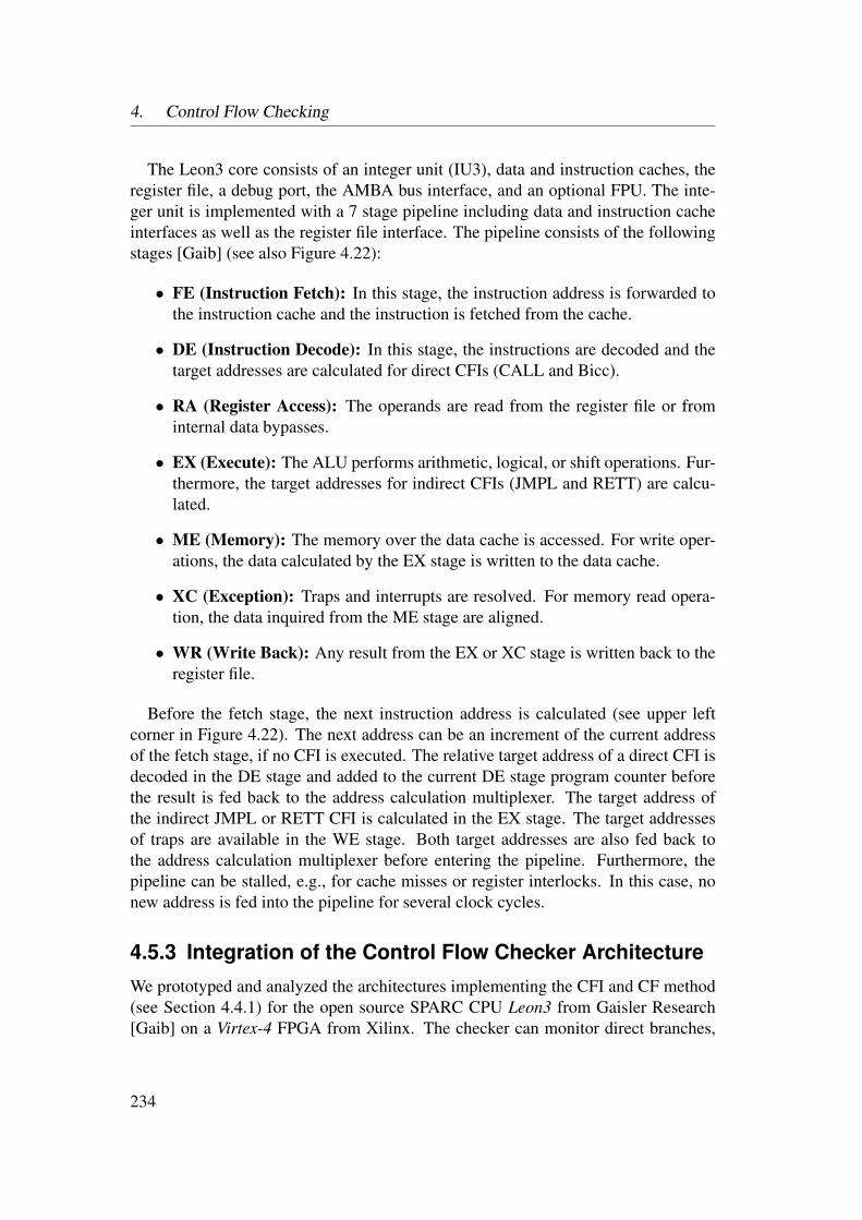
4. Control Flow Checking
The Leon3 core consists of an integer unit (IU3), data and instruction caches, theregister file, a debug port, the AMBA bus interface, and an optional FPU. The inte-ger unit is implemented with a 7 stage pipeline including data and instruction cacheinterfaces as well as the register file interface. The pipeline consists of the followingstages [Gaib] (see also Figure 4.22):
• FE (Instruction Fetch): In this stage, the instruction address is forwarded tothe instruction cache and the instruction is fetched from the cache.
• DE (Instruction Decode): In this stage, the instructions are decoded and thetarget addresses are calculated for direct CFIs (CALL and Bicc).
• RA (Register Access): The operands are read from the register file or frominternal data bypasses.
• EX (Execute): The ALU performs arithmetic, logical, or shift operations. Fur-thermore, the target addresses for indirect CFIs (JMPL and RETT) are calcu-lated.
• ME (Memory): The memory over the data cache is accessed. For write oper-ations, the data calculated by the EX stage is written to the data cache.
• XC (Exception): Traps and interrupts are resolved. For memory read opera-tion, the data inquired from the ME stage are aligned.
• WR (Write Back): Any result from the EX or XC stage is written back to theregister file.
Before the fetch stage, the next instruction address is calculated (see upper leftcorner in Figure 4.22). The next address can be an increment of the current addressof the fetch stage, if no CFI is executed. The relative target address of a direct CFI isdecoded in the DE stage and added to the current DE stage program counter beforethe result is fed back to the address calculation multiplexer. The target address ofthe indirect JMPL or RETT CFI is calculated in the EX stage. The target addressesof traps are available in the WE stage. Both target addresses are also fed back tothe address calculation multiplexer before entering the pipeline. Furthermore, thepipeline can be stalled, e.g., for cache misses or register interlocks. In this case, nonew address is fed into the pipeline for several clock cycles.
4.5.3 Integration of the Control Flow Checker Architecture
We prototyped and analyzed the architectures implementing the CFI and CF method(see Section 4.4.1) for the open source SPARC CPU Leon3 from Gaisler Research[Gaib] on a Virtex-4 FPGA from Xilinx. The checker can monitor direct branches,
234
4.5 Prototypical Implementation
alu/shift mul/div
y
register file
D-cacheaddress/dataoutdatain
3232
operand2rs1
imm
Ywres
result m_y
Decode
Execute
Memory
Write-back
rs2rs1
rd
tbr, wim, psr
30 jmpl address
e pc
30
+1
d_pc
jmpa
f_pc
Add
call/branch address
tbr‘0’
e_pc
m_pc
w_pc
d_inst
e_inst
m_inst
w_inst
Fetch
I-cacheaddressdata
Register Access
x_yxres
Exception
x_pcx_inst
r_pcr_inst
y, tbr, wim, psr
r_imm
Figure 4.22: The Leon3 integer unit pipeline. On the left side, the control paths areshown with the calculation of the next instruction address in the upperleft corner. On the right side, the data paths with the interface to thedata cache are shown [Gaib].
jumps and calls as well as indirect returns and also has the ability to re-execute acorrupted jump or branch instruction by fetching it again from the memory. Otherfeatures of the checker are the support of the activate and deactivate procedures de-scribed in Section 4.4.1. The complete implementation for control flow checking ofthe Leon3 core consists of the proposed architectures of checking of direct jumps andbranches (Section 4.4.1), the return stack (Section 4.4.2) and the repair mechanism(Section 4.4.6). To minimize the resource overhead, some features can be disabled(see Section 4.5.8). Indirect jumps which are not returns, are not supported so far,but many application programs or routines in embedded systems have none of theseinstructions, or should avoid their use.
235

4. Control Flow Checking
Implementation Overview
The implementation consists of a control path checker module (cpc basicReEx) andthe logic for re-execution in the integer pipeline of the Leon3 processor (iu3) (seeFigure 4.23). The different modular architectures of control flow checking are imple-mented into this checker module. The interface of this unit is kept generic, so the unitcan in principle be attached to any embedded RISC processor. For the Leon3 core,the checker module is attached to the integer pipeline.
Figure 4.23 shows the interface between the integer unit (iu3) of the Leon3 coreand the checker module. Also, an interface to the on-chip AMBA bus is shownwhich enables the access to the checker memories from the processor and debuggerside. Furthermore, Figure 4.24 shows the connection of the checker module interfaceto the integer pipeline, which is part of the iu3 module.
proc3
iu3cpc_basicReEx
cpc_cfLut
cpc_returnStack
Instruction Cache Interface (ICI)
AMBA Bus
PCn / PC
n+1
VALID
BRANCH
TRAP
RETT
CPCREEX
CPCREEXCODE
CPCREEXPC
ERROR
CPCEN
cpcAmba
Re-execution
logic
Figure 4.23: An overview of the control flow checker unit with the interface to theLeon3 integer unit (iu3). Each module (box) represents a VHDL mod-ule. All additional modules for the control flow checker are shown ingray.
The current program counter value (PCn) and the next program counter value(PCn+1) are taken from the first pipeline stages of the Leon3 core (see Figure 4.24).The current program counter for the checker is the program counter in the decode
236

4.5 Prototypical Implementation
PCn
PCn+1
+1
Fetch PC
Jump Addr
Branch Addr
Decode PC
Execute PC
Memory PC
Decode Inst
Execute Inst
Memory Inst
Control Flow
Checker
InstructionCache
Reg. Access PCReg. Access I.
Except. PCExcep. Inst
Write PCWrite Inst
Re-Execute PC
Memory Inst
Figure 4.24: The checker unit is placed between the first two pipeline stages of theLeon3 core [Gaib]. All bold lines denote new signal paths needed formonitoring and re-execution of jump and branch instructions.
pipeline step and the next program counter is the program counter of the fetch pipelinestep. For re-executing a jump or branch, the re-execution program counter from thechecker unit is fed to the program counter generation (a step prior to the fetch step),and the erroneous instructions are annulled, so the incorrect instructions are not exe-cuted and no registers or memories are written.
Checker Module (cpc basicReEx)
The general control flow checker (cpc basicReEx) consists of the control flow lookuptable (cfLut), the return stack (returnStack) and the checker logic. Additionally, anAMBA slave interface is included.
The interface of the checker module is depicted in Figure 4.23. The VALID sig-nal should be only active if the CURRPC and NEXTPC values are valid. For eachexecuted instruction, the VALID signal should be high for exactly one clock cycle.CURRPC is the current program counter and NEXTPC the next program counter.Both signals are taken from the instruction cache interface. The NEXTPC is the pro-gram counter after the fetch stage; CURRPC denotes the program counter before the
237
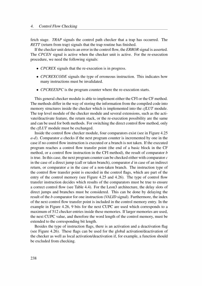
4. Control Flow Checking
fetch stage. TRAP signals the control path checker that a trap has occurred. TheRETT (return from trap) signals that the trap routine has finished.
If the checker unit detects an error in the control flow, the ERROR signal is asserted.The CPCEN signal is active when the checker unit is active. For the re-executionprocedure, we need the following signals:
• CPCREX signals that the re-execution is in progress.
• CPCREXCODE signals the type of erroneous instruction. This indicates howmany instructions must be invalidated.
• CPCREEXPC is the program counter where the re-execution starts.
This general checker module is able to implement either the CFI or the CF method.The methods differ in the way of storing the information from the compiled code intomemory structures inside the checker which is implemented into the cfLUT module.The top level module of the checker module and several extensions, such as the acti-vate/deactivate feature, the return stack, or the re-execution possibility are the sameand can be used for both methods. For switching the direct control flow method, onlythe cfLUT module must be exchanged.
Inside the control flow checker module, four comparators exist (see in Figure 4.25a-d). Comparator a checks if the next program counter is incremented by one in thecase if no control flow instruction is executed or a branch is not taken. If the executedprogram reaches a control flow transfer point (the end of a basic block in the CFmethod, or a control flow instruction in the CFI method), the result of comparator bis true. In this case, the next program counter can be checked either with comparator cin the case of a direct jump (call or taken branch), comparator d in case of an indirectreturn, or comparator a in the case of a non-taken branch. The instruction type ofthe control flow transfer point is encoded in the control flags, which are part of theentry of the control memory (see Figure 4.25 and 4.26). The type of control flowtransfer instruction decides which results of the comparators must be true to ensurea correct control flow (see Table 4.4). For the Leon3 architecture, the delay slots ofdirect jumps and branches must be considered. This can be done by delaying theresult of the b comparator for one instruction (VALID signal). Furthermore, the indexof the next control flow transfer point is included in the control memory entry. In theexample in Figure 4.26, 9 bits for the next CUPC are used which corresponds to amaximum of 512 checker entries inside these memories. If larger memories are used,the next CUPC value, and therefore the word length of the control memory, must beextended to the corresponding bit length.
Besides the type of instruction flags, there is an activation and a deactivation flag(see Figure 4.26). These flags can be used for the global activation/deactivation ofthe checker as well as local activation/deactivation if, for example, a function shouldbe excluded from checking.
238
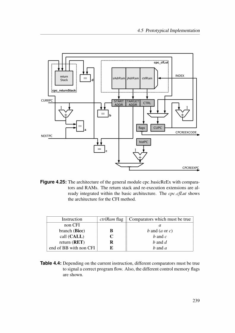
4.5 Prototypical Implementation
CURRPC
NEXTPC
a
c
TARGETADDR
b
STARTADDR CTRL
jAdrRamsAdrRam ctrlRam
=
=
=
+
1
+
1
CUPC
d=returnStack
flags
INDEX
+
1
histPC
CPCREEXCODE
CPCREEXPC
cpc_cfLut
cpc_returnStack
Figure 4.25: The architecture of the general module cpc basicReEx with compara-tors and RAMs. The return stack and re-execution extensions are al-ready integrated within the basic architecture. The cpc cfLut showsthe architecture for the CFI method.
Instruction ctrlRam flag Comparators which must be truenon CFI a
branch (Bicc) B b and (a or c)call (CALL) C b and creturn (RET) R b and d
end of BB with non CFI E b and a
Table 4.4: Depending on the current instruction, different comparators must be trueto signal a correct program flow. Also, the different control memory flagsare shown.
239

4. Control Flow Checking
D A E R C B next CUPC15 14 13 12 11 10 9 8 0
15 : Deactivate CPC14 : Activate CPC13 : Unused12 : End of Basic Block without CFI11 : Return from Subroutine10 : Call subroutine9 : Branch
8..0 : next CUPC
Figure 4.26: Control memory (ctrlRam) entry. The flags in the front denote the kindof the control flow transfer point. The last 9 bits represents the indexfor the next control flow point in case of a call or branch instruction.
If a trap occurs during the execution, which is signaled by the TRAP input, thechecker unit deactivates itself and the checker will be activated again by leaving thetrap routine (RETT signal).
Furthermore, logic and registers for the re-execution procedure are included inthe top level of the control path checker module. If the re-execution is triggered bya control transfer point, the correct start address is taken as the re-execution startaddress. If not, the value of a history register is taken which saves the last executedprogram counter (see Figure 4.25).
Control Flow LUT (cpc cfLut)
The only difference between the architecture of the CF and CFI method is in thecontrol flow LUT which implements the information of the control flow graph or thecontrol flow instruction graph. For both methods, the cfLut has the same interface,but different implementations. The LUT has also an AMBA bus interface to allowfor access to the LUT from the processor side.
The interface consists of the following signals: STARTADDR is the address ofthe next control flow transfer point and TARGETADDR is the corresponding targetaddress if the instruction is a direct jump or branch. CTRL is the control vector withthe control flags and the index of the next control flow point if the jump is executed(e.g., call or branch taken), as depicted in Figure 4.26. INDEX is the address of thechecker memories and the next values are fetched when the NEXTVALUE signal isactive. We need the VALID signal for the CF method, because the CF method needstwo clock cycles to fetch or calculate all values from the RAMs.
The implementation of the control flow LUT is depicted for the CFI method inFigure 4.25 and for the CF method in Figure 4.27.
240
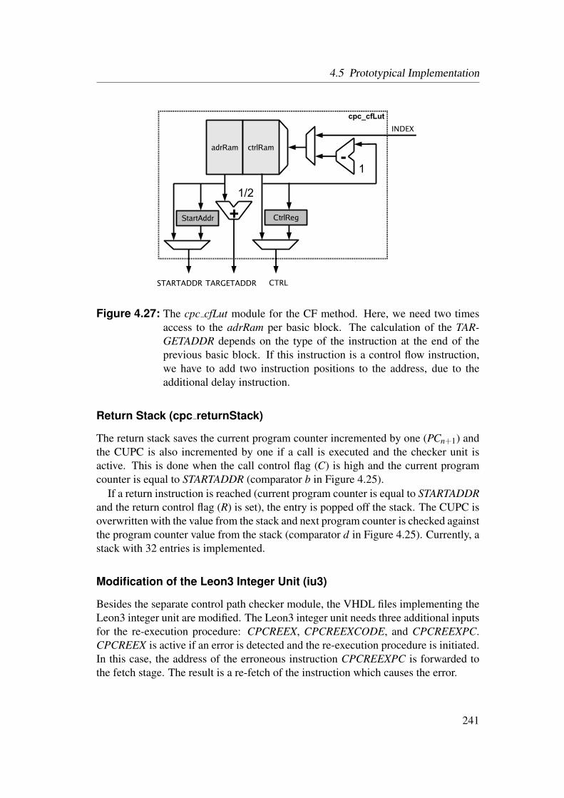
4.5 Prototypical Implementation
adrRam ctrlRam
+1/2
-1
cpc_cfLut
INDEX
STARTADDR TARGETADDR CTRL
StartAddr CtrlReg
Figure 4.27: The cpc cfLut module for the CF method. Here, we need two timesaccess to the adrRam per basic block. The calculation of the TAR-GETADDR depends on the type of the instruction at the end of theprevious basic block. If this instruction is a control flow instruction,we have to add two instruction positions to the address, due to theadditional delay instruction.
Return Stack (cpc returnStack)
The return stack saves the current program counter incremented by one (PCn+1) andthe CUPC is also incremented by one if a call is executed and the checker unit isactive. This is done when the call control flag (C) is high and the current programcounter is equal to STARTADDR (comparator b in Figure 4.25).
If a return instruction is reached (current program counter is equal to STARTADDRand the return control flag (R) is set), the entry is popped off the stack. The CUPC isoverwritten with the value from the stack and next program counter is checked againstthe program counter value from the stack (comparator d in Figure 4.25). Currently, astack with 32 entries is implemented.
Modification of the Leon3 Integer Unit (iu3)
Besides the separate control path checker module, the VHDL files implementing theLeon3 integer unit are modified. The Leon3 integer unit needs three additional inputsfor the re-execution procedure: CPCREEX, CPCREEXCODE, and CPCREEXPC.CPCREEX is active if an error is detected and the re-execution procedure is initiated.In this case, the address of the erroneous instruction CPCREEXPC is forwarded tothe fetch stage. The result is a re-fetch of the instruction which causes the error.
241

4. Control Flow Checking
The CPCREEXCODE denotes the kind of erroneous instruction. A non controlflow instruction is encoded with “00”, a direct call or branch is encoded with “10”and a return from subroutine is encoded with “01”. If the re-executed instruction isa direct call or branch, the current register window pointer CWP from the decodestage must be restored from the access stage so to ensure that the CWP has the samevalue before the erroneous instruction was executed. Also the integer condition codesicc must be restored. In case of an erroneous return from subroutine instruction, theCWP must be restored from the execute stage.
At last, the erroneous and the following instructions must be invalidated. This canbe done by setting the annul bit at the corresponding stage. In case of a direct call orbranch, the annul bit is set for the decode, register access, and execute stage and incase of an indirect return from subroutine, the annul bit for decode, register access,execute, memory and exception stage must be set. If the erroneous instruction wasnot a control flow instruction, only the decode stage must be invalidated.
4.5.4 A Tool for Program AnalysisTo prepare an application for control flow checking, the compiled code is analyzed bya program called “AISTool” which decodes the instructions and searches for controlflow instructions. This tool is able to generate the content of the checker memoriesfor the CF and the CFI cfLut module. The functions of the analyzed program whichshould be checked (user functions) can be specified in a separate file which is com-mitted to the analyzer program. The program first extracts all functions and searchesfor the user functions.
For the CFI method, all CFIs of the user functions are extracted and their addressesare stored in the sAdrRam initialization file and the destination address, except for thereturn instruction, is stored in the jAdrRam initialization file. For the CF method, theanalyzed program is first structured into basic blocks. The basic block end addressesare stored in the adrRam initialization file. For both methods, the correspondinginitialization file for the control Ram (ctrlRam) is generated. If a user function isleft by a call to a non user function, the checker will be deactivated and activatedagain on the back-jump. This is done by setting the corresponding activate (A) anddeactivate (D) flags in the control memory. Furthermore, the call to the first defineduser function (usually main()) which is the starting point for the checker is searchedand at this call, the checker unit will be activated. The index of this call must be’0’, because after global reset, the value at address ’0’ is loaded from the checkermemories. Finally, the memory initialization files and, optionally, a graph (CFG orCFIG) of the analyzed functions in the Graphviz .dot format [AR] are written. Theanalyzed application program remains completely unchanged.
The memory initialization files can be used for the synthesis of the checker unit,or for Xilinx FPGAs, the content of the rams can be initialized directly in the bitfileusing the Xilinx tool “data2mem”. We also implemented an AMBA bus interface
242
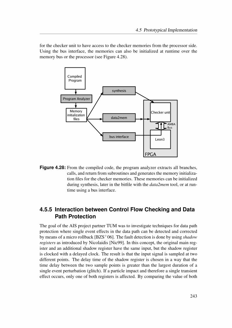
4.5 Prototypical Implementation
for the checker unit to have access to the checker memories from the processor side.Using the bus interface, the memories can also be initialized at runtime over thememory bus or the processor (see Figure 4.28).
Figure 4.28: From the compiled code, the program analyzer extracts all branches,calls, and return from subroutines and generates the memory initializa-tion files for the checker memories. These memories can be initializedduring synthesis, later in the bitfile with the data2mem tool, or at run-time using a bus interface.
4.5.5 Interaction between Control Flow Checking and DataPath Protection
The goal of the AIS project partner TUM was to investigate techniques for data pathprotection where single event effects in the data path can be detected and correctedby means of a micro rollback [BZS+06]. The fault detection is done by using shadowregisters as introduced by Nicolaidis [Nic99]. In this concept, the original main reg-ister and an additional shadow register have the same input, but the shadow registeris clocked with a delayed clock. The result is that the input signal is sampled at twodifferent points. The delay time of the shadow register is chosen in a way that thetime delay between the two sample points is greater than the largest duration of asingle event perturbation (glitch). If a particle impact and therefore a single transienteffect occurs, only one of both registers is affected. By comparing the value of both
243
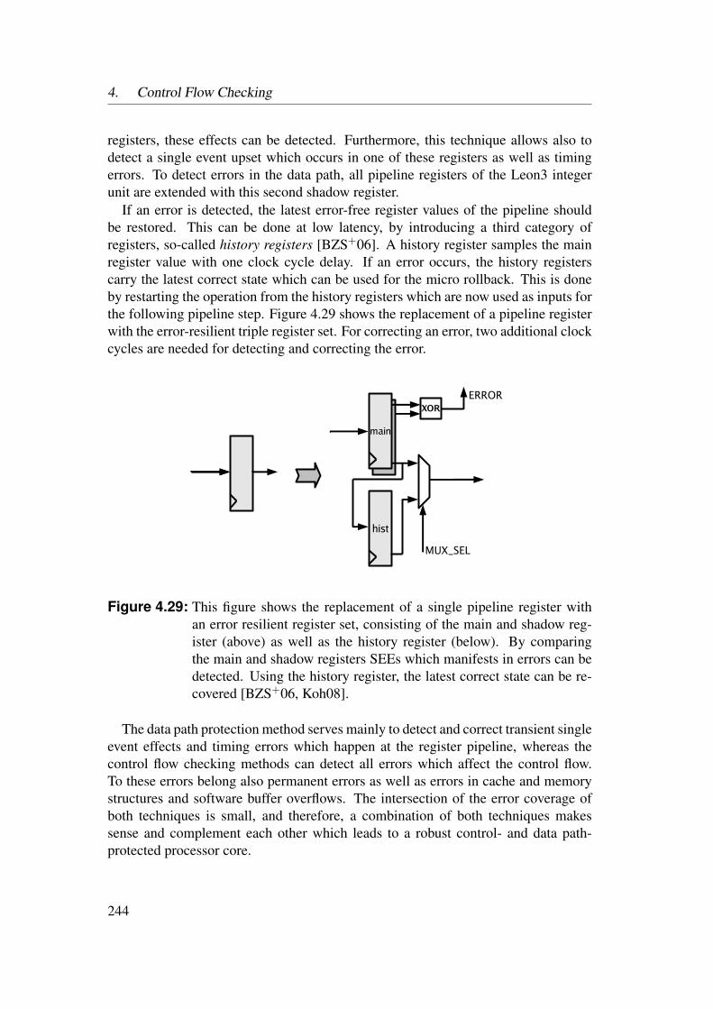
4. Control Flow Checking
registers, these effects can be detected. Furthermore, this technique allows also todetect a single event upset which occurs in one of these registers as well as timingerrors. To detect errors in the data path, all pipeline registers of the Leon3 integerunit are extended with this second shadow register.
If an error is detected, the latest error-free register values of the pipeline shouldbe restored. This can be done at low latency, by introducing a third category ofregisters, so-called history registers [BZS+06]. A history register samples the mainregister value with one clock cycle delay. If an error occurs, the history registerscarry the latest correct state which can be used for the micro rollback. This is doneby restarting the operation from the history registers which are now used as inputs forthe following pipeline step. Figure 4.29 shows the replacement of a pipeline registerwith the error-resilient triple register set. For correcting an error, two additional clockcycles are needed for detecting and correcting the error.
ERRORXOR
main
hist
MUX_SEL
Figure 4.29: This figure shows the replacement of a single pipeline register withan error resilient register set, consisting of the main and shadow reg-ister (above) as well as the history register (below). By comparingthe main and shadow registers SEEs which manifests in errors can bedetected. Using the history register, the latest correct state can be re-covered [BZS+06, Koh08].
The data path protection method serves mainly to detect and correct transient singleevent effects and timing errors which happen at the register pipeline, whereas thecontrol flow checking methods can detect all errors which affect the control flow.To these errors belong also permanent errors as well as errors in cache and memorystructures and software buffer overflows. The intersection of the error coverage ofboth techniques is small, and therefore, a combination of both techniques makessense and complement each other which leads to a robust control- and data path-protected processor core.
244

4.5 Prototypical Implementation
However, both techniques cannot easily be combined without modification, be-cause the error correction of one method affects the error detection of the othermethod. For example, consider a micro rollback of the data path protection causedby an error. The currently executed instruction is stalled and executed again, whichis identified by the control flow checker as a control flow error. It is obvious that themethod must communicate its correction action to the complementary method. Here,we cover only the control flow checking method. The question is how the controlflow checker deals with a micro rollback of the data path protection.
The easiest way is to deactivate the checker on a micro rollback and activate thechecker again after the reconstruction of a correct state. This can be easily done byevaluating a rollback signal from the data path protection control unit. The disadvan-tage is that during the rollback, the control flow checker unit is deactivated and thecontrol paths of the processor are unprotected.
The second possibility is to check also the control flow of the micro rollback.As mentioned before, the micro rollback consists of two steps. The first step is thedetection and freeze step. After successful detection of a data path error, the pipelineis stalled and the data path protection feeds the value of the history register of the fetchstep back to the program counter generation step in order to start the micro rollback(see Figure 4.30). From the control flow checker view, the PCn+1 input is set backto the PCn−1 value. To get this value, we can use the registered value from the PCninput. Actually, if the control flow re-execute feature is implemented, we alreadyhave such a register (histPC) that is used for the re-execution program counter value.To check the first rollback step, a new comparator f is introduced, which checks thecorrect new next program counter value in order to start the rollback [Koh08] (seeFigure 4.31).
The next step is the retry step, where the input of all pipeline stages is switched tothe history registers and as a result, the state of the data pipeline is rolled back to thestate before the error occurs. From the control flow checker view, the last instructionis executed again. The internal state of the control flow checker has also changed,hence, the state of this checker unit must also be rolled back. This can be done byintroducing history registers for the registers used inside the checker unit (see Figure4.31). For checking the control flow of the retried instruction, the values from thesehistory registers must be used. After successfully verifying the rollback, the controlflow checking unit is switched back to the normal registers just as the other registersof the data path pipeline.
If an (control path) error occurs during the micro rollback, the control flow checkeris able to correct this error by initializing a re-execution. If the error happens in thedetection/freeze step, the re-execution starts from the histPC register. However, ifthe error is inside this register, we have a problem which cannot be solved using thisarchitecture. A possible solution is to protect this register with an error correctingcode (ECC) or provide an additional redundant register. If the error occurs during thesecond rollback step, the normal re-execution procedure of the control flow checker
245
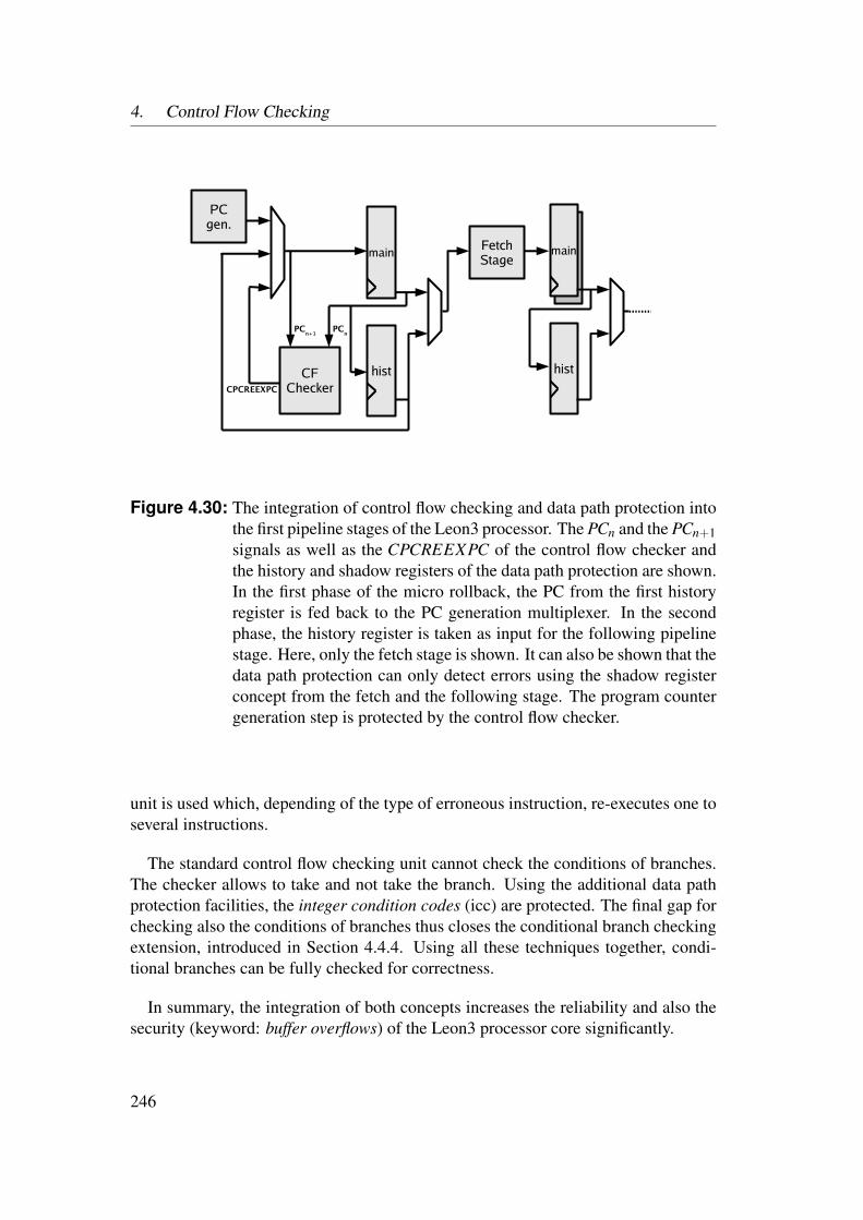
4. Control Flow Checking
main
CFCheckerCPCREEXPC
hist
PCgen.
PCn+1
PCn
FetchStage
main
hist
Figure 4.30: The integration of control flow checking and data path protection intothe first pipeline stages of the Leon3 processor. The PCn and the PCn+1signals as well as the CPCREEXPC of the control flow checker andthe history and shadow registers of the data path protection are shown.In the first phase of the micro rollback, the PC from the first historyregister is fed back to the PC generation multiplexer. In the secondphase, the history register is taken as input for the following pipelinestage. Here, only the fetch stage is shown. It can also be shown that thedata path protection can only detect errors using the shadow registerconcept from the fetch and the following stage. The program countergeneration step is protected by the control flow checker.
unit is used which, depending of the type of erroneous instruction, re-executes one toseveral instructions.
The standard control flow checking unit cannot check the conditions of branches.The checker allows to take and not take the branch. Using the additional data pathprotection facilities, the integer condition codes (icc) are protected. The final gap forchecking also the conditions of branches thus closes the conditional branch checkingextension, introduced in Section 4.4.4. Using all these techniques together, condi-tional branches can be fully checked for correctness.
In summary, the integration of both concepts increases the reliability and also thesecurity (keyword: buffer overflows) of the Leon3 processor core significantly.
246
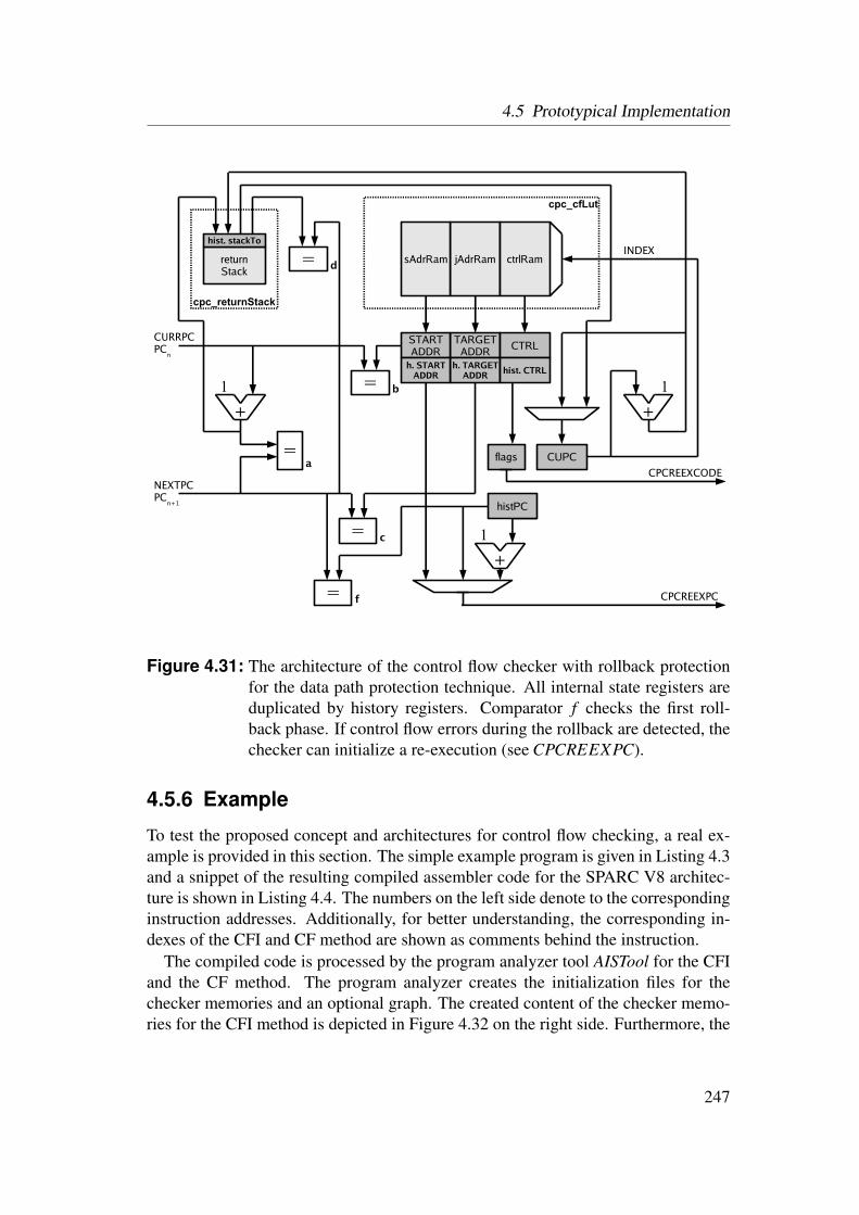
4.5 Prototypical Implementation
CURRPCPC
n
NEXTPCPC
n+1
a
c
TARGETADDR
b
STARTADDR CTRL
jAdrRamsAdrRam ctrlRam
=
=
=
+
1
+
1
CUPC
d=returnStack
flags
INDEX
+
1
histPC
CPCREEXCODE
CPCREEXPC
cpc_cfLut
cpc_returnStack
h. TARGETADDR
h. STARTADDR hist. CTRL
f=
hist. stackTo
Figure 4.31: The architecture of the control flow checker with rollback protectionfor the data path protection technique. All internal state registers areduplicated by history registers. Comparator f checks the first roll-back phase. If control flow errors during the rollback are detected, thechecker can initialize a re-execution (see CPCREEXPC).
4.5.6 Example
To test the proposed concept and architectures for control flow checking, a real ex-ample is provided in this section. The simple example program is given in Listing 4.3and a snippet of the resulting compiled assembler code for the SPARC V8 architec-ture is shown in Listing 4.4. The numbers on the left side denote to the correspondinginstruction addresses. Additionally, for better understanding, the corresponding in-dexes of the CFI and CF method are shown as comments behind the instruction.
The compiled code is processed by the program analyzer tool AISTool for the CFIand the CF method. The program analyzer creates the initialization files for thechecker memories and an optional graph. The created content of the checker memo-ries for the CFI method is depicted in Figure 4.32 on the right side. Furthermore, the
247

4. Control Flow Checking
Listing 4.3 Example program written in C
1 int inc = 0;2
3 void incr () 4 inc++;5 6
7 int main (int argc, char** argv) 8 while (inc < 3) 9 incr();
10 11
Listing 4.4 The compiled example program for the SPARC V8 architecture
1 40001054: call 40001180 <main> !CFI index: 0, CF index: 02 40001058: nop3 ...4 4000116c: restore !CF index: 15
6 40001170 <incr>:7 40001170: save %sp, -104, %sp8 40001174: inc %g19 40001178: ret !CFI index: 1, CF index: 2
10 4000117c: restore11
12 40001180 <main>:13 40001180: save %sp, -104, %sp !CF index: 314 40001184: cmp %g1, 215 40001188: bg 400011a0 !CFI index: 2, CF index: 416 4000118c: nop17 40001190: call 40001170 <incr> !CFI index: 3, CF index: 518 40001194: nop19 40001198: b 40001184 !CFI index: 4, CF index: 620 4000119c: nop21 400011a0: ret !CFI index: 5, CF index: 722 400011a4: restore
248
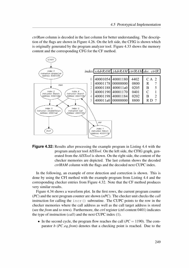
4.5 Prototypical Implementation
ctrlRam column is decoded in the last column for better understanding. The descrip-tion of the flags are shown in Figure 4.26. On the left side, the CFIG is shown whichis originally generated by the program analyzer tool. Figure 4.33 shows the memorycontent and the corresponding CFG for the CF method.
sAdrRAM jAdrRAM ctrlRAM
4000105440001178400011884000119040001198400011a0
4000118000000000400011a0400011704000118400000000
4402 08000205040102028800
index
012345
dec. ctrlR.
C A 2R ?B 5C 1B 2R D ?
Figure 4.32: Results after processing the example program in Listing 4.4 with theprogram analyzer tool AISTool. On the left side, the CFIG graph, gen-erated from the AISTool is shown. On the right side, the content of thechecker memories are depicted. The last column shows the decodedctrlRAM column with the flags and the decoded next CUPC index.
In the following, an example of error detection and correction is shown. This isdone by using the CFI method with the example program from Listing 4.4 and thecorresponding checker entries from Figure 4.32. Note that the CF method producesvery similar results.
Figure 4.34 shows a waveform plot. In the first rows, the current program counter(PC) and the next program counter are shown (nPC). The checker unit checks the callinstruction for calling the incr() subroutine. The CUPC points to the row in thechecker memories where the call address as well as the call target address is stored(see the from and to rows). Furthermore, the ctrl register (ctrl content 0401) indicatesthe type of instruction (call) and the next CUPC index (1).
• In the second cycle, the program flow reaches the call (PC = 1190). The com-parator b (PC eq from) denotes that a checking point is reached. Due to the
249

4. Control Flow Checking
adrRAM ctrlRAM
400010544000116c4000117840001180400011884000119040001198400011a0
44038000080010040207040202048800
index
01234567
dec. ctrlR.
C A 3D 2R ?E 4B 7C 2B 4R D ?
Figure 4.33: The results after processing the example program in Listing 4.4 withthe program analyzer tool AISTool for the CF method. On the left sidethe generated CFG is shown and on the right side the correspondingchecker memory content.
delay slot concept of the SPARC architecture, the call is executed in the nextcycle.
• In the third cycle, the call is first executed correctly (nPC = 1170), but thenan error occurs. The correct next program counter address 1170 is falsifiedto 3170. The error is detected by the checker unit because the comparator c(nPC eq to) is not longer true.
• In the forth cycle, the detected error is indicated by the error signal and the re-execution procedure is initialized. The starting point of the re-execution is thecall instruction (address 1190) which is shown by the reexPC signal. The reex-code signal indicates that the falsified instruction was a call, and therefore, thelatest three instructions in the pipeline should be annulled. This is done by an-nulling the decode (d.annull), the register access (a.annull), and the execution(e.annull) pipeline stages.
250

4.5 Prototypical Implementation
nPC
clk
PC
valid
nPC_eq_PC++
PC_eq_from
nPC stackTo_eq_
nPC_eq_to
reexPC
ctrl
from
to
stackCUPC
1190
118c
1194
1190
1170
1194 3170
1194
CUPC
stackTo
1190
1170
0401
03
105c
01
branch
error
reexcode
a.annull
11a0
1188
0205
02
3170
d.annull
e.annull
m.annull
x.annull
histPC
1170
1194
1174
1170
04
1178
0000
0800
01
1198
1190
1190
1190
10 0000
1188 1190 1194 3170 11941190118c
118c 1190 1194 3174 11981194
Figure 4.34: An example waveform showing the execution of the example programfrom Listing 4.4. During the execution of the call instruction on ad-dress 1190, an error occurs. The checker unit detects this error andstarts the re-execution procedure which corrects the error [Koh08].
251

4. Control Flow Checking
• In the fifth cycle, the call is executed again.
• In the sixth cycle, the jump is performed without error (comparator c is high).
After successfully executing the call, the values for the next checking point, the returninstruction with index 1 is loaded into the register from, to, and ctrl. Furthermore, itis also shown that the back-jump address for the return is put on the stack (stackTo =1198).
4.5.7 Simulation and Verification
In this section, we will discuss the verification of our control flow checker usingsimulation. For testing the handling of faults and errors with our control path checker,we need a fault model and methods for fault and error injection. The fault model andthe different kinds of fault and error injection are discussed in Section 4.2. For theverification, only intentional fault injections are used.
Fault and Error Injection
Now, we present the implementation of different kinds of fault and error injectionmethods as introduced in Section 4.2.
Permanent Memory Errors: The memory content of the SDRAM is stored forsimulation in *.srec files (sram.srec, sdram.srec, and prom.srec). TheVHDL model of the external SDRAM reads the content from these files during thesimulation. To inject permanent memory errors for simulation, we can alter the*.srec file. The checker memories of the checker unit which store the controlflow graph or control flow instruction graph, are generated using Xilinx Core Gen-erator (coregen) [Xilg]. The content of these checker memories is stored in *.miffiles for simulation. Here, we can also alter these files to inject permanent memoryerrors.
To generate permanent memory errors on the FPGA implementation, we can fur-ther use the in-circuit debugger of the Leon3 processor. Using this debugger, we areable to change the contents of all memory cells which are writable and mapped tothe address space of the processor over the AMBA bus interface. Since this appliesto the main memory of the processor system and the checker memories, it is easy toalter values and memory contents in this way.
Transient on Chip Processor Faults: There are two different ways to injecttransient faults for simulation. The first method is to use a simulator built-in com-mand to set a signal to a specific value. In Modelsim 6.3e, the command is calledforce.
252

4.5 Prototypical Implementation
VSIM> force -freeze signame forceval forcetime -cancel releasetime
The signal signame is forced to the value forceval at forcetime until releasetime.The freeze parameter indicates that the original signal value is overwritten with force-val.
The second method to inject transient faults into the processor system is to use afault injection unit instantiated in the integer pipeline of the Leon3. The injection unitcan inject multiple faults in the control path on the same signals as the simulationcommand method (rin.d.pc). The faults are triggered by a PRNG (see Section4.2 and [Koh08]). This method is able to inject single event transitions (SET) on a(pseudo-)random time with (pseudo-)random duration. This is done using the VHDLstatements wait for and transport after. Because of the usage of thesestatements, the method is only working in simulation.
A synthesizable injection unit is coupled with the clock frequency. This restrictsus to use a free time pattern for fault injection. We inject faults on the same signalsas in the fault injection methods above. For triggering the injection, we use a 5-bitcounter. If the counter overflows and the integer pipeline of the Leon3 executes aninstruction, a fault is injected. The processor executes approximately one instructionevery 5 clock cycles in average. But this pattern is very irregular due to pipelinestalls caused by cache misses, branches, bus arbitration and so on. The combinationof both, the counter overflow and the irregular pattern of execution of instructions,generates a (pseudo-)random distribution of injected faults.
Testbench and Verification
To verify the correctness of the checker unit by simulation, we are using the Leon3debug log. With the debug log enabled, the Leon3 simulation model prints the addressand name of every executed instruction on the ModelSim console. The output of theconsole can be logged into a file. If the debug log with and without fault or errorinjection is the same, the checker unit passes the test for the used test program.
For the complete verification, we used several test programs. These test programsare pbm and qsort from the Mibench benchmark [GRE+01] and the turbo decoderfrom AIS project partner TU Kaiserslautern (adapted from [BGT93]). We are usingthe counter fault injection method, because of this method is synthesizable. We canuse this method for simulation and for an FPGA implementation. On the FPGAimplementation, we check the output which is transferred over the RS232 link to thePC and compare it with the run without error injection.
Table 4.5 shows the simulation results of the test programs. Each program is ex-ecuted twice, one run without and one run with error injection. The number of exe-cuted instructions and the overall clock cycles are measured. With these values, theCPI (Clocks per Instruction) value can be calculated. Furthermore, the number of in-jected errors are depicted. It can been shown that the CPI value increases with enabled
253
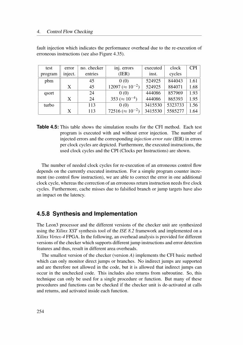
4. Control Flow Checking
fault injection which indicates the performance overhead due to the re-execution oferroneous instructions (see also Figure 4.35).
test error no. checker inj. errors executed clock CPIprogram inject. entries (IER) inst. cycles
pbm 45 0 (0) 524925 844043 1.61X 45 12097 (≈ 10−2) 524925 884071 1.68
qsort 24 0 (0) 444086 857969 1.93X 24 353 (≈ 10−4) 444086 865393 1.95
turbo 113 0 (0) 3415530 5323733 1.56X 113 72516 (≈ 10−2) 3415530 5585277 1.64
Table 4.5: This table shows the simulation results for the CFI method. Each testprogram is executed with and without error injection. The number ofinjected errors and the corresponding injection error rate (IER) in errorsper clock cycles are depicted. Furthermore, the executed instructions, theused clock cycles and the CPI (Clocks per Instructions) are shown.
The number of needed clock cycles for re-execution of an erroneous control flowdepends on the currently executed instruction. For a simple program counter incre-ment (no control flow instruction), we are able to correct the error in one additionalclock cycle, whereas the correction of an erroneous return instruction needs five clockcycles. Furthermore, cache misses due to falsified branch or jump targets have alsoan impact on the latency.
4.5.8 Synthesis and Implementation
The Leon3 processor and the different versions of the checker unit are synthesizedusing the Xilinx XST synthesis tool of the ISE 8.2 framework and implemented on aXilinx Virtex-4 FPGA. In the following, an overhead analysis is provided for differentversions of the checker which supports different jump instructions and error detectionfeatures and thus, result in different area overheads.
The smallest version of the checker (version A) implements the CFI basic methodwhich can only monitor direct jumps or branches. No indirect jumps are supportedand are therefore not allowed in the code, but it is allowed that indirect jumps canoccur in the unchecked code. This includes also returns from subroutine. So, thistechnique can only be used for a single procedure or function. But many of theseprocedures and functions can be checked if the checker unit is de-activated at callsand returns, and activated inside each function.
254

4.5 Prototypical Implementation
0,00
E+000
2,00
E-003
4,00
E-003
6,00
E-003
8,00
E-003
1,00
E-002
1,20
E-002
1,40
E-002
1,4
1,5
1,6
1,7
1,8
1,9
2
2,1
pbmqsortturbo
IER
CP
I
Figure 4.35: Plot of the number of cycles per instruction (CPI) over the injectederror rate (IER) according to the results reported in Table 4.5 for thethree test programs.
The second version (version B) has an additional 32-entry return stack extension.With this version, we can also monitor calls and returns, so most application programscan be fully monitored.
The last version (version C) has the additional capability of repairing an incorrectcontrol flow by re-execution (re-execution extension).
Table 4.6 shows the measured resource overheads of these three versions. Theresults show that the area overhead for logic (in terms of lookup tables and flip-flops) is very small compared to the amount of resources needed by the processorcore. If more control flow instructions shall be monitored and more checker memoryentries are needed, only the overhead of necessary block rams (BRAMs) increases.Using the CF methods instead of the CFI, the area overhead increases slightly for thesame maximum number of checker memory entries whereas the memory overheaddecreases. Note that typically, the CF method needs more checker entries than theCFI method for the same program. The bus interface for the AMBA bus creates anadditional area overhead of 68 LUTs and 5 flip-flops which can be subtracted fromthe values above if the bus interface is not needed.
The overhead values above consider the control flow checker implementationsonly. If these methods should be combined with the data path protection technolo-gies as described in Section 4.5.5, the area overhead increases. For example, a CFImethod in version C configuration (with return stack and re-execution extension)which is able to check also the micro rollback from the data path protection needs
255
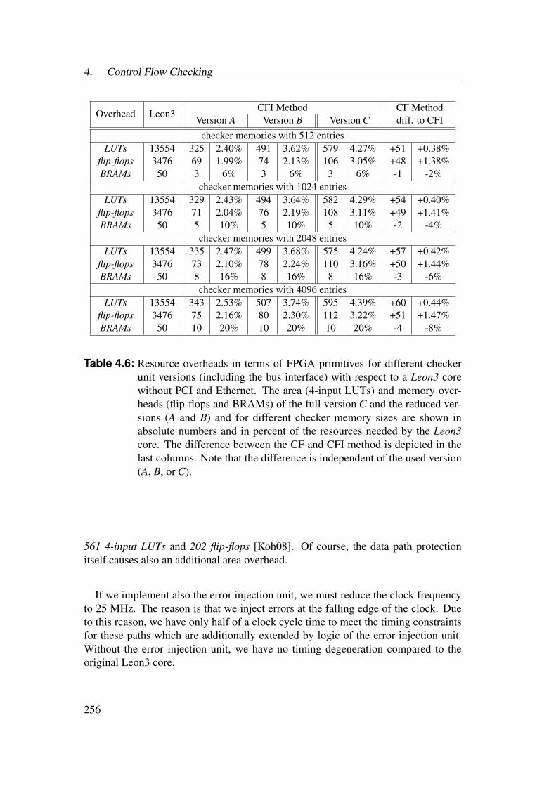
4. Control Flow Checking
Overhead Leon3CFI Method CF Method
Version A Version B Version C diff. to CFIchecker memories with 512 entries
LUTs 13554 325 2.40% 491 3.62% 579 4.27% +51 +0.38%flip-flops 3476 69 1.99% 74 2.13% 106 3.05% +48 +1.38%BRAMs 50 3 6% 3 6% 3 6% -1 -2%
checker memories with 1024 entriesLUTs 13554 329 2.43% 494 3.64% 582 4.29% +54 +0.40%
flip-flops 3476 71 2.04% 76 2.19% 108 3.11% +49 +1.41%BRAMs 50 5 10% 5 10% 5 10% -2 -4%
checker memories with 2048 entriesLUTs 13554 335 2.47% 499 3.68% 575 4.24% +57 +0.42%
flip-flops 3476 73 2.10% 78 2.24% 110 3.16% +50 +1.44%BRAMs 50 8 16% 8 16% 8 16% -3 -6%
checker memories with 4096 entriesLUTs 13554 343 2.53% 507 3.74% 595 4.39% +60 +0.44%
flip-flops 3476 75 2.16% 80 2.30% 112 3.22% +51 +1.47%BRAMs 50 10 20% 10 20% 10 20% -4 -8%
Table 4.6: Resource overheads in terms of FPGA primitives for different checkerunit versions (including the bus interface) with respect to a Leon3 corewithout PCI and Ethernet. The area (4-input LUTs) and memory over-heads (flip-flops and BRAMs) of the full version C and the reduced ver-sions (A and B) and for different checker memory sizes are shown inabsolute numbers and in percent of the resources needed by the Leon3core. The difference between the CF and CFI method is depicted in thelast columns. Note that the difference is independent of the used version(A, B, or C).
561 4-input LUTs and 202 flip-flops [Koh08]. Of course, the data path protectionitself causes also an additional area overhead.
If we implement also the error injection unit, we must reduce the clock frequencyto 25 MHz. The reason is that we inject errors at the falling edge of the clock. Dueto this reason, we have only half of a clock cycle time to meet the timing constraintsfor these paths which are additionally extended by logic of the error injection unit.Without the error injection unit, we have no timing degeneration compared to theoriginal Leon3 core.
256
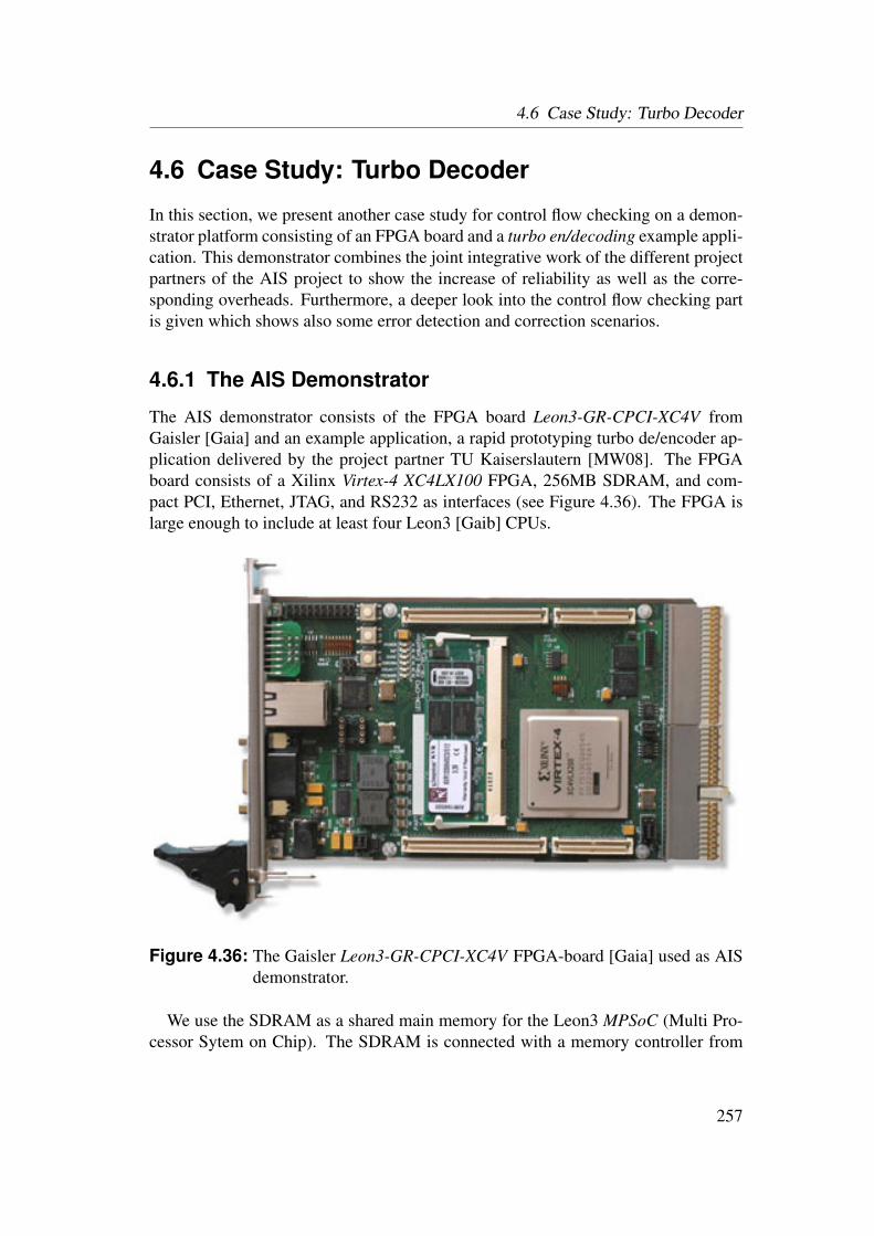
4.6 Case Study: Turbo Decoder
4.6 Case Study: Turbo Decoder
In this section, we present another case study for control flow checking on a demon-strator platform consisting of an FPGA board and a turbo en/decoding example appli-cation. This demonstrator combines the joint integrative work of the different projectpartners of the AIS project to show the increase of reliability as well as the corre-sponding overheads. Furthermore, a deeper look into the control flow checking partis given which shows also some error detection and correction scenarios.
4.6.1 The AIS Demonstrator
The AIS demonstrator consists of the FPGA board Leon3-GR-CPCI-XC4V fromGaisler [Gaia] and an example application, a rapid prototyping turbo de/encoder ap-plication delivered by the project partner TU Kaiserslautern [MW08]. The FPGAboard consists of a Xilinx Virtex-4 XC4LX100 FPGA, 256MB SDRAM, and com-pact PCI, Ethernet, JTAG, and RS232 as interfaces (see Figure 4.36). The FPGA islarge enough to include at least four Leon3 [Gaib] CPUs.
Figure 4.36: The Gaisler Leon3-GR-CPCI-XC4V FPGA-board [Gaia] used as AISdemonstrator.
We use the SDRAM as a shared main memory for the Leon3 MPSoC (Multi Pro-cessor Sytem on Chip). The SDRAM is connected with a memory controller from
257
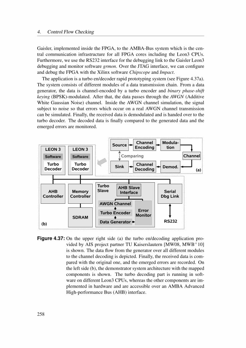
4. Control Flow Checking
Gaisler, implemented inside the FPGA, to the AMBA-Bus system which is the cen-tral communication infrastructure for all FPGA cores including the Leon3 CPUs.Furthermore, we use the RS232 interface for the debugging link to the Gaisler Leon3debugging and monitor software grmon. Over the JTAG interface, we can configureand debug the FPGA with the Xilinx software Chipscope and Impact.
The application is a turbo en/decoder rapid prototyping system (see Figure 4.37a).The system consists of different modules of a data transmission chain. From a datagenerator, the data is channel-encoded by a turbo encoder and binary phase-shiftkeying (BPSK)-modulated. After that, the data passes through the AWGN (AdditiveWhite Gaussian Noise) channel. Inside the AWGN channel simulation, the signalsubject to noise so that errors which occur on a real AWGN channel transmissioncan be simulated. Finally, the received data is demodulated and is handed over to theturbo decoder. The decoded data is finally compared to the generated data and theemerged errors are monitored.
TurboSlaveAHB
ControllerMemory
Controller
SDRAM
AHB SlaveInterface Serial
Dbg Link
RS232
Turbo Encoder
AWGN Channel
ErrorMonitor
Data Generator
LEON 3
Software
LEON 3
Software
TurboDecoder
TurboDecoder
Source
Channel
Sink
ChannelEncoding
Modula-tion
ChannelDecoding Demod.
Comparing
(a)
(b)
Figure 4.37: On the upper right side (a) the turbo en/decoding application pro-vided by AIS project partner TU Kaiserslautern [MW08, MWB+10]is shown. The data flow from the generator over all different modulesto the channel decoding is depicted. Finally, the received data is com-pared with the original one, and the emerged errors are recorded. Onthe left side (b), the demonstrator system architecture with the mappedcomponents is shown. The turbo decoding part is running in soft-ware on different Leon3 CPUs, whereas the other components are im-plemented in hardware and are accessible over an AMBA AdvancedHigh-performance Bus (AHB) interface.
258

4.6 Case Study: Turbo Decoder
This system is mapped into our demonstrator architecture (see Figure 4.37b). Thedata generator, turbo encoder, AWGN channel, and the error monitor are imple-mented as a hardware module inside the FPGA. The channel and the error monitorare connected to the AMBA bus. The turbo decode module is implemented in soft-ware running on one or more Leon3 CPUs. The data to and from the turbo decoderis transmitted over the AMBA Bus. Additionally, the main memory (SDRAM) isconnected to the AMBA Bus over the memory controller.
With this architecture, we are able to evaluate and demonstrate the autonomousunits developed for the AIS project. We can inject faults into the AMBA bus com-munication and the control and data paths of the Leon3 CPUs.
4.6.2 Control Flow Checking Contribution
For the control flow protected Leon3 CPU, we implemented the VHDL model of theCFI method with the return stack, re-execution, and bus interface extensions. To em-ulate control path errors, we used a synthesizable error injection unit based on a 5-bitcounter as introduced in Section 4.5.7. The number of detected and corrected errorsis recorded by an error counter which is accessible from software over a memory-mapped register. Also, the fault injection unit can be switched on or off by software,by setting a certain bit in a control register. The status of the fault injection unit isshown in the output of the software which is transferred over a RS232 link and canbe displayed using a serial terminal program. Also, the read values from the errorcounter register as well as a clock cycle and executed instructions counter register aredisplayed.
Additionally, the program counter signals from the first pipeline steps as well asthe CPCREEX (see Section 4.5.3) signal which shows that a re-execution procedureis in progress, are recorded and can be displayed with the Xilinx debugging toolChipscope.
Measuring the executed instructions and clock cycles when the turbo decodingsoftware is executed shows us that the average CPI (clocks per instructions) increaseswhen the error injection is switched on due to additional clock cycles for correctingerrors than without error injection (see Table 4.7). An additional latency of 4.7 clockcycles on average for each injected error is measured.
Figure 4.38 shows screenshots from Chipscope. In the upper trace (a), a fault isinjected at a non control flow instruction. The normal sequence from 0x40001F68over 0x40001F6C to 0x40001F70 is interrupted by an error of the program counter(0x40009F6C). The checker unit has detected this error and re-executes the erro-neous instruction (0x40001F6C).
In the trace below (b), the error is the wrong target (0x40009898 instead of0x40001898) of a branch (0x40001EA8). In this case, the error is also detectedand the branch is re-executed. Note that 0x40001EAC is the delay instruction.
259
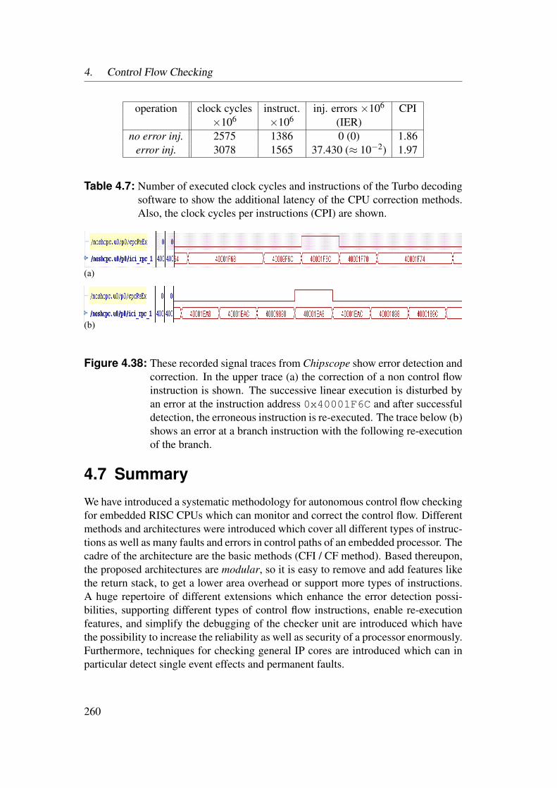
4. Control Flow Checking
operation clock cycles instruct. inj. errors ×106 CPI×106 ×106 (IER)
no error inj. 2575 1386 0 (0) 1.86error inj. 3078 1565 37.430 (≈ 10−2) 1.97
Table 4.7: Number of executed clock cycles and instructions of the Turbo decodingsoftware to show the additional latency of the CPU correction methods.Also, the clock cycles per instructions (CPI) are shown.
(a)
(b)
Figure 4.38: These recorded signal traces from Chipscope show error detection andcorrection. In the upper trace (a) the correction of a non control flowinstruction is shown. The successive linear execution is disturbed byan error at the instruction address 0x40001F6C and after successfuldetection, the erroneous instruction is re-executed. The trace below (b)shows an error at a branch instruction with the following re-executionof the branch.
4.7 Summary
We have introduced a systematic methodology for autonomous control flow checkingfor embedded RISC CPUs which can monitor and correct the control flow. Differentmethods and architectures were introduced which cover all different types of instruc-tions as well as many faults and errors in control paths of an embedded processor. Thecadre of the architecture are the basic methods (CFI / CF method). Based thereupon,the proposed architectures are modular, so it is easy to remove and add features likethe return stack, to get a lower area overhead or support more types of instructions.A huge repertoire of different extensions which enhance the error detection possi-bilities, supporting different types of control flow instructions, enable re-executionfeatures, and simplify the debugging of the checker unit are introduced which havethe possibility to increase the reliability as well as security of a processor enormously.Furthermore, techniques for checking general IP cores are introduced which can inparticular detect single event effects and permanent faults.
260

4.7 Summary
Implementations of some of these embedded processor checking modules wereprovided which can monitor and correct direct jumps and branches as well as returnsfrom subroutine. Experimental results show that the additional hardware overhead isquite small. In particular, lookup tables and flip-flops overhead amount to an over-head of less than 5% of the CPU core requirements in all cases. So, the actual over-head results from the additional memory needed to monitor the control flow instruc-tions. According to Michel et al. [MLS91], the Cerberus-16 processor has a memoryoverhead of 34-85%, whereas the WDP approach has an overhead of 24-61% (seeSection 2.4.2). Our control flow checking approach has a memory overhead of only15-30% according results reported in Table 4.2. Please note that these values are onlycomparable with care due to different processor architectures and benchmarks. Fur-thermore, the values from Table 4.2 do not include the overhead for the instructionintegrity checker (IIC). When also considering the IIC, the memory overhead of ourmethod is increased by approximate 5-10%.
A modular concept for generation of generic micro-programmable checker unitshas been proposed, so the area overhead can be further reduced by removing somemodular components. The detection of errors happens during the execution of theerroneous instruction, so we have the possibility to react immediately and prevent anyincorrect instruction from being executed. Furthermore, an incorrect jump or branchinstruction can be re-fetched and re-executed. With this technique, we therefore haveno performance impact on the CPU in the error-free case and the compiled programcode remains also unchanged.
In our implementations, an independent program counter CUPC with its own statemachine and own micro-code with own micro-instructions (ctrlRam) was introduced.The checker micro-program code is based on the extracted branch and jump instruc-tions from the program code. This reduced code covers only direct branches or jumpswithout the instructions between two branch points. With this technique, we en-hanced the CPU with a reduced second independent program counter and instructionunit at minimum additional hardware cost and full control of the program flow. Theapproach of Arora et al. [ARRJ06] has some similarities with our approach. Theadvantages of ours, however, is that we are a) more flexible in using memories tostore the control flow (instruction) graph instead of synthesizing a dedicated finitestate machine (FSM) in logic for each program to be executed. Moreover, we have b)no performance impact in the error-free case, and c) our checker unit is simpler andthus requires less resources. Compared to all existing approaches, however, the mainadvantage is the tight integration into the processor, which enables us to detect errorsvery fast and before the error manifests into the register of the processor which oftenmight be too late to circumvent failures or attacks. This allows us also to immediatelycorrect an error by a simple re-execution of the last instructions.
Finally, using the bus interface of the checker unit, the contents or part of thecontent of the checker memories might also be stored in the system memory insteadof dedicated memories. Only the content for checking the current part of the program
261

4. Control Flow Checking
(e.g., the current function or a set of functions which are current in use) may beheld in the local checker memories. If the checker needs information which is notstored inside the checker memories, the checker can generate a page-fault-like eventto signal the operating system to reload the these memories with the needed contents.This concept of caching can reduce the memory overhead significantly.
262
5Conclusions
This dissertation provides an overview of security and reliability issues for IP coresin embedded systems. Potential faults and attacks, which cause common securityand reliability problems, were classified. Major contributions of this thesis are noveltechniques for IP protection of cores and control flow checking for RISC processorcores.
The justification of the existence of such methods which clearly cause additionaloverhead and costs, are the ongoing technical advances of the underlying semicon-ductor technology. These advances lead, on the one hand, to more complex systems,consisting of billions of transistors. On the other hand, the individual transistors arebecoming more and more unreliable in new technology generations due to increasedprocess variation, accelerated aging, and increased sensitivity for single event effects.Current design methodologies like worst-case design flow or proprietary interfacescannot keep up with this development. New design methodologies are needed tohandle these challenges for systems using billions of transistors, which include themassive reuse of designs and cores. Interface standardization of IP cores will bea huge topic in the future, which will provide solutions, but also cause problems.Standardized IP core interfaces will boost the growth of the already vast market forreusable IP cores for ASIC and FPGA technologies enormously. Clearly, the ques-tion of confidentiality and protection against unlicensed usage of IP cores is becomingmore and more important. Our presented watermarking techniques can be a solutionto this problem for several IP cores. Furthermore, these complex systems consistingof manifold kinds of IP cores, such as processors, bus systems, interface cores, hard-ware accelerators, stand on shaky ground. The decreased reliability of the individualtransistors leads to the loss of faith that the underlying semiconductor technology,
263

5. Conclusions
combined with the corresponding verified design flow are error-free. The well knownworst case design flow is not longer applicable. Future designs and systems must dealwith the unreliable foundation they are built upon. They have to autonomously reactto environmental changes, and monitor faults. In other words, future designs musttake care of the underlying resources by using them resource-aware. However, thisresource-aware autonomous methodology needs new design paradigms which resultsin a redesign of existing cores. To circumvent the need to redesign, existing coresmust be extended by additional elements to implement this autonomous behavior.The control flow checking methodology proposed in this thesis provides one of theseunits which is able to monitor faults and errors caused by the underlying unreliabletechnology and which can correct them autonomously.
Summary
A brief summary of the three parts of this dissertation is given as follows:
• Overview of Security and Reliability Issues for Embedded Systems: InChapter 1, security and reliability problems for embedded systems are ana-lyzed and described. Basic definitions in the area of security, and dependabil-ity are given. A taxonomy of faults and attacks in embedded systems is pre-sented and the severity of these issues is emphasized, in particular for futuretechnology generations. In Chapter 2, related work on techniques to increasesecurity and reliability is presented. In focus are techniques for IP protectionand countermeasures for code injection attacks which corresponds to securityissues, as well as common techniques for increasing the reliability of IP coresin embedded systems. Finally, control flow checking techniques for embeddedprocessors are discussed which combine security and reliability issues.
• Watermarking and Identification Techniques for FPGA IP Cores: In Chap-ter 3, novel IP core watermarking and identification techniques for FPGA de-signs are presented. These techniques were developed in order to detect anunlicensed usage of IP cores. First, a general watermarking model, introducedby Li et al. [LMS06], is extended and adapted to watermarking and identifi-cation of IP cores used in the electronic design automation flow. Techniquesfor identification of HDL and netlist cores as well as approaches for water-marking of netlist and bitfile cores are proposed. All these methods have incommon that only the FPGA bitfile is needed from the company suspected ofIP fraud. Moreover, novel watermarking techniques that verify the authorshipby monitor the power consumption, so-called power watermarking, are intro-duced. Starting from a basic approach, many different encoding and decodingmethods are analyzed. Furthermore, different multiplexing techniques for con-current sending of different watermarked cores, combined in the same FPGA,
264
are investigated. Finally, the effectiveness, but also the additional costs areconfirmed by experimental results.
• Control Flow Checking for Embedded RISC Processors: In Chapter 4,new methods, architectures, and implementations for autonomous control flowchecking in embedded RISC processors are described. First, an overview ofthe project Autonomous Integrated Systems (AIS) and some initial remarks forfault injection are given. After that, methods and architectures for control flowchecking of all types of control flow instructions in embedded RISC cores andcommon IP cores are introduced. For direct jumps and branches, two alterna-tive methods are proposed which form a basis architecture. This basis architec-ture can be extended towards support of indirect jumps, detecting more types oferrors, or error correction measures. An example implementation of the basiscontrol flow checker for RISC processors as well as many extensions is shownfor the Leon3 SPARC V8 core. Moreover, the interaction with a data path pro-tection scheme and the corresponding overheads are elaborated. Finally, a casestudy consisting of an error protected multi-processor rapid prototyping plat-form which implements a turbo encoding/decoding system is demonstrated.
Future Directions
Security and reliability issues in embedded systems are becoming more and moreimportant with future generations of semiconductor technology. Therefore, the needfor methods and concepts as presented in this dissertation, will increase. However,there are several extensions to these methods and new techniques which worth toinvestigate in the future.
In the area of IP protection, several links are still missing to complete the chainfor identification of HDL cores in FPGA bitfiles. The identification of netlist coresin the FPGA bitfile and the comparison of different netlists in order to decide if theywere generated from the same source is possible. Future work might bring bothmethods together to identify HDL cores in bitfiles. Another interesting technique isto verify watermarks using electromagnetic radiation. The advantages over powerwatermarking techniques are an easy measurement without soldering wires onto thePCB board, and the raster scanning over the FPGA area which provides additionalgeometric location information. Power watermarking techniques can be further im-proved by investigation of new encoding and decoding methods in order to be moreresistant against noise and disturbances. Furthermore, these techniques can be usedto transfer general data from the cores out of the FPGA. Power communication mightbe useful if a communication possibility must be added later in the development andno further dedicated pins of the FPGA or wires on the board are available. Possi-ble applications include monitoring core status information or debugging. With themethods presented in this dissertation, we achieve data transfer rates of up to 500
265

5. Conclusions
kbit/s. Finally, all these watermarking and identification techniques can be bundledinto a framework which can be tightly integrated with the design flow in developmentenvironments.
Future research in the context of control flow checking techniques for embeddedRISC processors might consider the minimization of the memory overhead, full sup-port for indirect jumps and support of other processor architectures. The memoryoverhead can be reduced by introducing hierarchical checker structures as, for exam-ple, in [ARRJ06], and compression methods. Using hierarchical checkers, relativeaddresses can be used and combined with memory compression algorithms and thus,the memory overhead can be drastically decreased. By using caching techniqueswhere the checker content is stored in the system memory and loaded into a cache-like on-chip memory for checking the current part or function, the amount of expen-sive on-chip memory can be further reduced. The reloading of the cache may bedone by the operation system or autonomously by the checker unit. The approachesfor checking indirect jumps can also benefit from the memory overhead reductiontechniques. Furthermore, the identification of valid indirect jump targets is also apotential area of future research. Finally, our control flow checking approaches canbe adapted to other types of processor architectures. In particular single instruction,multiple data (SIMD) architectures and multi-cores which execute the program syn-chronously in parallel are suitable for our checking approach. On these architectures,only one checker unit is needed which reduces the relative hardware overhead.
Finally, the IP core watermarking techniques are applicable only to FPGA targetsand design flow, whereas the reliability methods presented in this dissertation arefocused on ASIC designs. The combination and adaption of both so to increase thereliability of FPGA designs might also be an interesting future area of research.
266

AGerman Part
Methoden zur Verbesserung derSicherheit und Zuverlassigkeitvon eingebetteten IP-Cores in
FPGA- und ASIC-Designs
267

A. German Part
268
Zusammenfassung
Die vorliegende Arbeit gibt einen Uberblick uber Sicherheits- und Zuverlassigkeits-aspekte in eingebetteten Systemen. Hierbei wurden mogliche Fehlerquellen und Si-cherheitsangriffe, sowie geeignete Gegenmaßnahmen aufgezeigt. Speziell wurdenneue Techniken zum Schutze geistigen Eigentums (engl. Intellectual Property – IP)von Schaltungsblocken sowie Kontrollflussuberwachungsmaßnahmen fur RISC Pro-zessoren untersucht.
Der Einsatz solcher Methoden, die zusatzliche Ressourcen benotigen und damitMehrkosten verursachen, ist notwendig und gerechtfertigt durch die Fortschritte inder Halbleitertechnologie. Diese Fortschritte erlauben komplexere Systeme, die ei-nerseits aus Milliarden von Transistoren bestehen konnen, jedoch andererseits mit je-der neuen Technologiegeneration immer unzuverlassiger werden. Grunde hierfur sindhohere Variationen in der Herstellung, eine schnellere Alterung, sowie eine hohereAnfalligkeit gegenuber sogenannten Single-Event-Effects. Heutige Entwurfsstrate-gien wie der Worst-Case Entwicklungsfluss oder proprietare Schnittstellen konnenmit dieser Entwicklung nicht mithalten. Um zum Beispiel Schaltungen zu beherr-schen, die aus Milliarden von Transistoren bestehen, mussen neue Entwurfsstrate-gien angewandt werden wie die massive Wiederverwendung von gekauften oderselbst geschriebenen Schaltungsblocken. Die Standardisierung der Schnittstellen vonSchaltungsblocken, die zwar Losungen bringt aber auch Probleme verursachen kann,wird eine Herausforderung sein. Das Wachstum des Markts von wiederverwendbarenSchaltungsblocken fur die FPGA oder ASIC Technologie wird durch die Standardi-sierung der Schnittstellen enorm beschleunigt. Naturlich wird dadurch auch die Fra-ge nach dem Schutz von geistigem Eigentum immer wichtiger. Die in dieser Arbeitvorgestellten Wasserzeichenmethoden konnen fur viele Schaltungsblocke eine Ant-wort auf diese Frage sein. Andererseits stehen diese komplexen Systeme – bestehendaus vielseitigen Schaltungsblocken wie Prozessoren, Bussen, Schnittstellenschaltun-gen, Hardwarebeschleunigern, usw. – auf wackligen Beinen. Dass die grundlegen-de Halbleitertechnologie kombiniert mit dem entsprechenden verifizierten Entwurfs-fluss fehlerfrei ist, kann durch die abnehmende Zuverlassigkeit der einzelnen Tran-sistoren nicht mehr sichergestellt werden. Der bekannte Worst-Case Entwurfsflussist in Zukunft nicht mehr anwendbar. Zukunftige Systeme mussen sich mit der un-zuverlassigen Halbleitertechnologie auf der sie aufbauen auseinandersetzen und au-tonom auf Anderungen der Umgebungsbedingungen sowie Fehler reagieren. Mit an-
269

A. German Part
deren Worten: Sie mussen auf die zugrundeliegende Halbleitertechnologie Rucksichtnehmen, indem sie diese ressourcengewahr verwenden. Diese neue autonome res-sourcengewahre Benutzung verlangt aber auch neuen Entwurfsparadigmen, welcheublicherweise einen Neuentwurf existierender Schaltungen nach sich zieht. Um dieszu verhindern, konnen auch existierende Schaltungen mit neuen Elementen, welchedieses autonome Verhalten bereit stellen, erweitert werden. Die in dieser Arbeit vor-gestellte Kontrollflussuberwachungseinheit ist eine solche autonome Einheit, die dementsprechenden Prozessor die Moglichkeit gibt, Fehler der zugrundeliegenden Halb-leitertechnologie zu erkennen, und diese selbststandig zu korrigieren.
Kapitelubersicht
Im Folgenden wird eine kurze Zusammenfassung der Kapitel gegeben:
• Sicherheits- und Zuverlassigkeitsaspekte in eingebetteten Systemen: In Ka-pitel 1 werden aktuelle Sicherheits- und Zuverlassigkeitsprobleme aufgezeigt,die in heutigen eingebetteten Systemen vorkommen. Dazu werden auch grund-legende Begriffe und Definitionen aus dem Sicherheits- und Verlasslichkeits-bereich, sowie mogliche Fehler und Sicherheitsangriffe vorgestellt. Die Wich-tigkeit dieser Aspekte, sowie die Notwendigkeit von Gegenmaßnahmen wirddadurch unterstrichen. Diese Maßnahmen werden in Kapitel 2 vorgestellt. ImMittelpunkt standen insbesondere Maßnahmen zum Schutz geistigen Eigen-tums, Gegenmaßnahmen fur sogenannte Code-Injection-Angriffe zur Erhohungder Sicherheit, sowie Maßnahmen um die Zuverlassigkeit von eingebettetenSchaltungen zu verbessern. Des Weiteren werden Kontrollflussuberwachungs-methoden vorgestellt, die gleichzeitig Sicherheits- als auch Zuverlassigkeitsas-pekte vereinen.
• Wasserzeichen und Identifikationsmethoden fur FPGA-Schaltungen: Ka-pitel 3 beschaftigt sich mit neuen Wasserzeichen- und Identifikationsmethodenzum Schutz geistigen Eigentums von FPGA-Schaltungsblocken. Diese Metho-den konnen eine nicht lizenzierte Verwendung des Schaltungsblocks aufde-cken. Zuerst wird ein von Li und anderen [LMS06] entwickeltes allgemeinesModell fur Wasserzeichenmethoden um Identifikationsvefahren fur elektrischeSchaltungen erweitert. Danach werden Identifikationsmethoden fur sogenann-te Netzlisten- und HDL-Schaltungsblocke, sowie Wasserzeichenmethoden furNetzlisten- und Bitfile-Schaltungsblocke vorgestellt. Alle diese Verfahren be-notigen nur das FPGA-Bitfile aus dem Produkt der Firma, die im Verdachtsteht, Schaltungsblocke anderer illegal einzusetzen. Des Weiteren wird ein neu-er Ansatz vorgestellt, bei dem das Wasserzeichen durch den Energieverbrauchdes FPGAs ausgelesen und verifiziert wird – das sogenannte Power Water-marking. Zuerst wird eine Basismethode dieses Verfahrens vorgestellt, die um
270

verschiedene Kodierungs- und Dekodierungsansatze erweitert wird. Zusatzlichwerden noch verschiedene Multiplexverfahren prasentiert, die ein gleichzeiti-ges Senden von mehreren Wasserzeichen verschiedener Schaltungsblocke ineinem FPGA erlauben. Zum Schluss werden die Kosten und die Funktionswei-se aller Methoden durch Experimente an Beispielschaltungen verifiziert.
• Kontrollflussuberwachung fur eingebettete RISC Prozessoren: In Kapi-tel 4 werden Methoden, Architekturen und Implementierungen fur autonomeKontrollflussuberwachung in eingebetteten Prozessoren vorgestellt. Diese Ver-fahren werden im Rahmen des Projekts Autonome Integrierte Systeme (AIS)untersucht, welches zu Beginn erortert wird. Zusatzlich werden grundlegen-de Aspekte zur Fehlerinjektion analysiert. Danach werden die Methoden undArchitekturen fur die Kontrollflussuberwachung vorgestellt, welche alle Ar-ten von Kontrollflussbefehlen eines eingebetteten RISC Prozessors abdecken.Dabei werden allgemeine Schaltungsblocke nicht außer Acht gelassen. Zweialternative Verfahren zur Uberwachung von direkten Sprungen und Verzwei-gungen bilden die Basisarchitekturen, welche durch zusatzliche Module zurUberwachung von indirekten Sprungen, Erkennung von anderen Arten vonFehlern oder Fehlerkorrekturmaßnahmen erweitert werden konnen. Eine bei-spielhafte Implementierung der Basisarchitekturen und einige Erweiterungenwurde fur den SPARC V8 Prozessor Leon3 realisiert. Zusatzlich wurde eineDatenpfaduberwachung in unsere Verfahren integriert und der zusatzliche Res-sourcenaufwand untersucht. Zum Schluss wird eine Fallstudie prasentiert, dieaus einem Multiprozessorsystem besteht, welches um unsere Fehlererkennungs-und Korrekturverfahren erweitert wurde, und auf dem eine Kodierungs- undDekodierungsanwendung nach dem Turbo-Verfahren ausgefuhrt wird.
Ausblick auf weiterfuhrende Themen
Auch mit zukunftigen Halbleitergenerationen werden Sicherheits- und Zuverlassig-keitsaspekte in eingebetteten Systemen immer wichtiger. Damit wird auch die Not-wendigkeit der in dieser Arbeit entwickelten Methoden und Konzepte steigen. Jedochist die Arbeit an diesen Methoden keinesfalls abgeschlossen und zukunftige Erweite-rungen und neue Techniken bieten genug Raum fur weitere Forschungen.
Auf dem Forschungsgebiet des Schutz geistigen Eigentums von FPGA-Schaltungs-blocken fehlen noch einige Glieder der vollstandigen Kette um HDL-Schaltungsblo-cke in einem FPGA-Bitfile ohne Wasserzeichen zu identifizieren. Die Identifikati-on von Netzlistenschaltungen in FGPA-Bitfiles, sowie die Entscheidung, ob mehrereNetzlistenschaltungen von dem gleichen HDL-Schaltungsblock generiert wurden, istjetzt schon moglich. In zukunftigen Arbeiten konnen diese beide Verfahren vereinigtwerden, um HDL-Schaltungblocke in FPGA-Bitfiles zu identifizieren. Das Ausle-sen und Verifizieren von Wasserzeichen mittels elektro-magnetischer Abstrahlung ist
271
A. German Part
auch ein interessantes zukunftiges Forschungsgebiet. Vorteile gegenuber dem Aus-lesen uber die Spannungsversorgung sind unter anderem das einfache Messen oh-ne aufwandige Lotarbeiten an der Platine und die Moglichkeit eines Abtasten derAbstrahlung an verschiedenen Stellen uber der FPGA-Flache, welches zusatzlichegeometrische Lokalisierungsinformationen liefert. Aber auch das Power Watermar-king Verfahren lasst sich mit neuen Kodierungs- und Dekodierungsmethoden er-weitern, um im Falle von Storungen noch bessere Dekodierungsergebnisse zu be-kommen. Daruber hinaus lassen sich diese Verfahren auch zur Ubertragung allge-meiner Daten aus dem FPGA einsetzen. Diese sogenannte Power Communicationkonnte dann in Fallen hilfreich sein, wenn diese Kommunikationsmoglichkeit erstspat in der Entwicklung eingesetzt werden muss und keine weiteren dafur vorgese-hene Pins oder Leitungen auf der Platine vorhanden sind. Mogliche Anwendungenwaren z.B. das Ubertragen von Uberwachungsinformationen des Schaltungblocksoder das Debuggen und Testen. Mit den in dieser Arbeit vorgestellten Verfahren las-sen sich Ubertragungsraten bis zu 500 kbit/s realisieren. Schließlich lassen sich al-le diese Wasserzeichen- und Identifikationsverfahren in einem Framework zusam-menfassen, welches in den bestehenden Entwicklungsumgebungen integriert werdenkann.
Weitere Forschungsrichtungen fur die Kontrollflussuberwachung von eingebette-ten RISC-Prozessoren sind die Minimierung des Speicheraufwands, die kompletteUnterstutzung von indirekten Sprungen, sowie die Unterstutzung von mehr Prozes-sorarchitekturen. Der Speicheraufwand kann durch hierarchische Uberwachungsstruk-turen, wie z.B. in [ARRJ06] und durch Kompressionsmethoden verringert werden.Hierarchische Uberwachungseinheiten verwenden relative Speicheradressen, wel-che zusatzlich durch Kompressionsverfahren weit weniger Speicher benotigen alsdie heutigen Methoden. Des Weiteren kann durch die Implementierung des Cache-Verfahrens der Bedarf des teuren On-chip-Speichers verringert werden. In diesemVerfahren werden die Informationen, die zur Uberwachung benotigt werden, im Sys-temspeicher abgelegt und zum Uberwachen einer gerade ausgefuhrten Funktion oderTeil des Programms in einen Cache-artigen On-chip-Speicher geladen. Das Wieder-auffullen des Caches mit neuen Daten kann durch das Betriebssystem oder selbst-standig von der Uberwachungseinheit veranlasst werden. Auch die Verfahren zurUberwachung von indirekten Sprungen konnen von den Speicherreduktionstechnikenprofitieren. Die automatische Identifizierung von indirekten Sprungzielen im Pro-gammcode ist auch ein mogliches zukunftiges Forschungsgebiet. Schließlich sollteauch die Portierung der hier vorgestellten Uberwachungseinheit auf anderen Pro-zessorarchitekturen untersucht werden. Vor allem Single-Instruction, Multiple-Data(SIMD) Architekturen und Multiprozessorsysteme, bei denen das Programm syn-chron parallel ausgefuhrt wird, eignen sich fur unseren Uberwachungsansatz, da indiesen Architekturen nur eine Uberwachungseinheit mehrere Ausfuhrungseinheitenkontrollieren kann.
272

Die in dieser Arbeit vorgestellten Wasserzeichenverfahren sind fur den FPGA-Entwurfsfluss entwickelt worden, wahrend die Methoden zur Verbesserung der Zu-verlassigkeit eher fur den ASIC-Entwurf ausgelegt sind. Eine Kombination und An-passung dieser Methoden um die Zuverlassigkeit von FPGA-Schaltungen zu verbes-sern konnte auch ein interessantes zukunftiges Forschungsgebiet sein.
273

A. German Part
274
Bibliography
[AAN00] Lorena Anghel, Dan Alexandrescu, and Michael Nicolaidis. Evalua-tion of a Soft Error Tolerance Technique based on Time and/or SpaceRedundancy. In Integrated Circuits and Systems Design, 2000. Pro-ceedings. 13th Symposium on, pages 237–242, 2000.
[AARR03] Dakshi Agrawal, Bruce Archambeault, Josyula R. Rao, and Pankaj Ro-hatgi. The EM Side-Channel(s). In CHES ’02: 4th International Work-shop on Cryptographic Hardware and Embedded Systems, pages 29–45, London, UK, 2003. Springer-Verlag.
[ABEL05] Martın Abadi, Mihai Budiu, Ulfar Erlingsson, and Jay Ligatti. Control-flow Integrity. In CCS ’05: Proceedings of the 12th ACM Confer-ence on Computer and Communications Security, pages 340–353, NewYork, NY, USA, 2005. ACM Press.
[ABEL09] Martın Abadi, Mihai Budiu, Ulfar Erlingsson, and Jay Ligatti. Control-flow Integrity: Principles, Implementations, and Applications. ACMTrans. Inf. Syst. Secur., 13(1):1–40, 2009.
[ABMF04] Todd Austin, David Blaauw, Trevor Mudge, and Krisztian Flautner.Making Typical Silicon Matter with Razor. Computer, 37(3):57–65,2004.
[ADM04] Sobeeh Almukhaizim, Petros Drineas, and Yiorgos Makris. Concur-rent Error Detection for Combinational and Sequential Logic via Out-put Compaction. In ISQED ’04: Proceedings of the 5th InternationalSymposium on Quality Electronic Design, pages 459–464, Washington,DC, USA, 2004. IEEE Computer Society.
[AGM+71] Algirdas Anthony Avizienis, GC Gilley, Francis Parkash Mathur,David Allen Rennels, JA Rohr, and DK Rubin. The STAR (self-testingand repairing) computer: An investigation of the theory and practiceof fault-tolerant computer design. IEEE Transactions on Computers,100(20):1312–1321, 1971.
275

Bibliography
[AHTA04] Amr T. Abdel-Hamid, Sofiene Tahar, and El Mostapha Aboulhamid. ASurvey on IP Watermarking Techniques. Design Automation for Em-bedded Systems, 9(3):211–227, 2004.
[Ajl95] Cheryl Ajluni. Two new Imaging Techniques Promise to Improve ICDefect Identification. Electronic Design, 43(14):37–38, 1995.
[AK96] Ross Anderson and Markus Kuhn. Tamper Resistance: A CautionaryNote. In WOEC’96: Proceedings of the 2nd conference on Proceedingsof the Second USENIX Workshop on Electronic Commerce, pages 1–11,Berkeley, CA, USA, 1996. USENIX Association.
[Ale96] Aleph One. Smashing the Stack for Fun and Profit. Phrack magazine,49(7), 1996.
[All00] VSI Alliance. Intellectual Property Protection White Paper: Schemes,Alternatives and Discussion Version 1.1. Issued by Intellectual Prop-erty Protection Development Working Group, Ver, 1.1, 2000.
[All07] Business Software Alliance. Fifth Annual BSA and IDC Global Soft-ware Piracy Study. Technical report, 2007.
[ALR01] Algirdas Avizienis, Jean-Claude Laprie, and Brian Randell. Funda-mental concepts of dependability. Technical Report Series – Universityof Newcastle upon Tyne Computing Science, 2001.
[ALRL04] Algirdas Avizienis, Jean-Claude Laprie, Brian Randell, and CarlLandwehr. Basic Concepts and Taxonomy of Dependable and SecureComputing. IEEE transactions on dependable and secure computing,pages 11–33, 2004.
[Alta] Altera. Error Detection and Recovery Using CRC in Altera FPGA De-vices. URL: http://www.altera.com/literature/an/an357.pdf.
[Altb] Altera. FPGA Design Security Solution Using MAX II Devices. URL:http://www.altera.com/literature/wp/wp_m2dsgn.pdf.
[And72] James P. Anderson. Computer Security Technology Planning Study,1972.
[ANKA99] Z. Alkhalifa, V. S. Sukumaran Nair, Narayanan Krishnamurthy, andJacob A. Abraham. Design and Evaluation of System-Level Checks forOn-Line Control Flow Error Detection. IEEE Trans. Parallel Distrib.Syst., 10(6):627–641, 1999.
276
Bibliography
[AR] AT&T-Research. Graphviz - Graph Visualization Software. URL:http://graphviz.org/.
[ARM99] ARM. AMBA specification (rev 2.0). ARM Limited, 1999.
[ARRJ06] Divya Arora, Srivaths Ravi, Anand Raghunathan, and Niraj K. Jha.Hardware-assisted Run-time Monitoring for Secure Program Execu-tion on Embedded Processors. IEEE Transactions on Very Large ScaleIntegration (VLSI) Systems, 14(12):1295–1308, 2006.
[ARS04] Andre Adelsbach, Markus Rohe, and Ahmad-Reza Sadeghi. Over-coming the Obstacles of Zero-knowledge Watermark Detection. InMM&Sec ’04: Proceedings of the 2004 workshop on Multimedia andsecurity, pages 46–55, New York, NY, USA, 2004. ACM.
[Aus95] Kenneth Austin. Data Security Arrangements for Semiconductor Pro-grammable Devices, February 7 1995. US Patent 5,388,157.
[Aus99] Todd M. Austin. DIVA: A Reliable Substrate for Deep Submicron Mi-croarchitecture Design. In MICRO 32: Proceedings of the 32nd annualACM/IEEE international symposium on Microarchitecture, pages 196–207, Washington, DC, USA, 1999. IEEE Computer Society.
[BA02] Michael L. Bushnell and Vishwani D. Agrawal. Essentials of Elec-tronic Testing for Digital, Memory, and Mixed-signal VLSI Circuits.Kluwer Academic, 2002.
[BAFS05] Elena Gabriela Barrantes, David H. Ackley, Stephanie Forrest, andDarko Stefanovic. Randomized Instruction Set Emulation. ACM Trans.Inf. Syst. Secur., 8(1):3–40, 2005.
[Bar] Scott Barrick. Designing Around an Encrypted Netlist: IsThe Pain Worth the Gain? D&R Industry Articles. URL:http://www.design-reuse.com/articles/18205/
encrypted-netlist.html.
[Bar81] Joel F. Bartlett. A NonStop Kernel. In SOSP ’81: Proceedings of theeighth ACM symposium on Operating systems principles, pages 22–29,New York, NY, USA, 1981. ACM.
[Bau05] Robert C. Baumann. Radiation-induced soft errors in advanced semi-conductor technologies. IEEE Transactions on Device and materialsreliability, 5(3):305–316, 2005.
277

Bibliography
[Bau08] Florian Baueregger. Identifikation von signierten Schaltungen an-hand von Leistungsverbrauchsmessungen. Dilpomarbeit, Departmentof Computer Science 12, University of Erlangen-Nuremberg, January2008.
[BBB+97] S. Buchner, M. Baze, D. Brown, D. McMorrow, J. Melinger, SFA Inc,and MD Largo. Comparison of Error Rates in Combinational andSequential Logic. IEEE Transactions on Nuclear Science, 44(6 Part1):2209–2216, 1997.
[BBC05] BBC. 1986: Coal Mine Canaries made Redundant. URL:http://news.bbc.co.uk/onthisday/hi/dates/stories/
december/30/newsid_2547000/2547587.stm, 2005.
[BDH+98] Feng Bao, Robert H. Deng, Yongfei Han, Albert B. Jeng, A. DesaiNarasimhalu, and Teow-Hin Ngair. Breaking Public Key Cryptosys-tems on Tamper Resistant Devices in the Presence of Transient Faults.In Proceedings of the 5th International Workshop on Security Proto-cols, pages 115–124, London, UK, 1998. Springer-Verlag.
[BDS03] Sandeep Bhatkar, Daniel C. DuVarney, and R. Sekar. Address Obfus-cation: An Efficient Approach to Combat a Broad Range of MemoryError Exploits. In SSYM’03: Proceedings of the 12th conference onUSENIX Security Symposium, pages 8–8, Berkeley, CA, USA, 2003.USENIX Association.
[BEA06] Mihai Budiu, Ulfar Erlingsson, and Martın Abadi. Architectural Sup-port for Software-based Protection. In ASID ’06: Proceedings of the 1stworkshop on Architectural and system support for improving softwaredependability, pages 42–51, New York, NY, USA, 2006. ACM.
[BGB06] Lilian Bossuet, Guy Gogniat, and Wayne Burleson. Dynamically Con-figurable Security for SRAM FPGA Bitstreams. International Journalof Embedded Systems, 2(1):73–85, 2006.
[BGT93] Claude Berrou, Alain Glavieux, and Punya Thitimajshima. Near Shan-non Limit Error-Correcting Coding and Decoding: Turbo-Codes. InProc. 1993 International Conference on Communications (ICC ’93),pages 1064–1070, Geneva, Switzerland, May 1993.
[BGXC07] Fujun Bai, Zhiqiang Gao, Yi Xu, and Xueyu Cai. A WatermarkingTechnique for Hard IP Protection in Full-custom IC Design. In Interna-tional Conference on Communications, Circuits and Systems (ICCCAS2007), pages 1177–1180, 2007.
278
Bibliography
[BK00] Bulba and Kil3r. Bypassing Stackguard and Stackshield. Phrack Mag-azine, 2000.
[BKIL03] Saurabh Bagchi, Zbigniew Kalbarczyk, Ravishankar Iyer, and Y. Lev-endel. Design and Evaluation of Preemptive Control Signature(PECOS) Checking. IEEE Transactions on Computers, 2003.
[BLW+01] Saurabh Bagchi, Y Liu, Keith Whisnant, Zbigniew Kalbarczyk, Rav-ishankar K. Iyer, Y. Levendel, and Larry Votta. A Framework forDatabase Audit and Control Flow Checking for a Wireless TelephoneNetwork Controller. In DSN ’01: Proceedings of the 2001 Interna-tional Conference on Dependable Systems and Networks (formerly:FTCS), pages 225–234, Washington, DC, USA, 2001. IEEE ComputerSociety.
[BM07] Jan A. Bergstra and C. A. Middelburg. Instruction Sequences withIndirect Jumps. Electronic Report PRG0709, Programming ResearchGroup, University of Amsterdam, 2007.
[Bor05] Shekhar Borkar. Designing Reliable Systems from Unreliable Compo-nents: The Challenges of Transistor Variability and Degradation. IEEEMicro, 25(6):10–16, 2005.
[BPS00] William R. Bush, Jonathan D. Pincus, and David J. Sielaff. A Static An-alyzer for Finding Dynamic Programming Errors. Software-PracticeExperience, 30(7):775–802, 2000.
[BRSS08] Erik Buchanan, Ryan Roemer, Hovav Shacham, and Stefan Savage.When Good Instructions go Bad: Generalizing Return-oriented Pro-gramming to RISC. In CCS ’08: Proceedings of the 15th ACM con-ference on Computer and communications security, pages 27–38, NewYork, NY, USA, 2008. ACM.
[BS97] Eli Biham and Adi Shamir. Differential Fault Analysis of Secret KeyCryptosystems. In CRYPTO ’97: Proceedings of the 17th Annual In-ternational Cryptology Conference on Advances in Cryptology, pages513–525, London, UK, 1997. Springer-Verlag.
[BSO07] Fred A. Bower, Daniel J. Sorin, and Sule Ozev. Online Diagnosis ofHard Faults in Microprocessors. ACM Transactions on Architectureand Code Optimization (TACO), 4(2):8, 2007.
[BSOS04] Fred A. Bower, Paul G. Shealy, Sule Ozev, and Daniel J. Sorin. Tolerat-ing Hard Faults in Microprocessor Array Structures. In DSN ’04: Pro-ceedings of the 2004 International Conference on Dependable Systems
279
Bibliography
and Networks, page 51, Washington, DC, USA, 2004. IEEE ComputerSociety.
[BSR09] Daniel Baldin, Katharina Stahl, and Franz Rammig. Ergebnisberichtuber Selbstorganisierende Betriebssysteme fur autonome IntegrierteSchaltungen. AIS Meilensteinbericht UPB-HNI-Q12, 2009.
[BST00] Arash Baratloo, Navjot Singh, and Timothy Tsai. Transparent Run-time Defense against Stack Smashing Attacks. In ATEC ’00: Proceed-ings of the annual conference on USENIX Annual Technical Confer-ence, pages 251–262, Berkeley, CA, USA, 2000. USENIX Associa-tion.
[BTH96] Laurence Boney, Ahmed H. Tewfik, and Khaled N. Hamdy. DigitalWatermarks for Audio Signals. In International Conference on Multi-media Computing and Systems, pages 473–480, 1996.
[BWWA06] Edson Borin, Cheng Wang, Youfeng Wu, and Guido Araujo. Software-Based Transparent and Comprehensive Control-Flow Error Detection.In CGO ’06: Proceedings of the International Symposium on CodeGeneration and Optimization, pages 333–345, Washington, DC, USA,2006. IEEE Computer Society.
[BZS+06] Abdelmajid Bouajila, Johannes Zeppenfeld, Walter Stechele, AndreasHerkersdorf, Andreas Bernauer, Oliver Bringmann, and WolfgangRosenstiel. Organic Computing at the System on Chip Level. In Pro-ceedings of the IFIP International Conference on Very Large Scale In-tegration of System on Chip (VLSI-SoC 2006). Springer, October 2006.
[BZSH09] Abdelmajid Bouajila, Johannes Zeppenfeld, Walter Stechele, and An-dreas Herkersdorf. Multi-bit Soft-and Timing Error Detection for CPUPipelines. In Proceedings of edaWorkshop 09. VDE VERLAG GmbH,2009.
[CBB+01] Crispin Cowan, Matt Barringer, Steve Beattie, Greg Kroah-Hartman,Mike Frantzen, and Jamie Lokier. FormatGuard: Automatic Protectionfrom printf Format String Vulnerabilities. In SSYM’01: Proceedingsof the 10th conference on USENIX Security Symposium, Berkeley, CA,USA, 2001. USENIX Association.
[CBD+99] Crispin Cowan, Steve Beattie, Ryan Finnin Day, Calton Pu, Perry Wa-gle, and Erik Walthinsen. Protecting Systems from Stack SmashingAttacks with StackGuard. In Linux Expo, 1999.
280

Bibliography
[CBJW03] Crispin Cowan, Steve Beattie, John Johansen, and Perry Wagle. Point-guardTM: Protecting Pointers from Buffer Overflow Vulnerabilities. InSSYM’03: Proceedings of the 12th conference on USENIX SecuritySymposium, Berkeley, CA, USA, 2003. USENIX Association.
[CD00] Roy Chapman and Tariq S. Durrani. IP Protection of DSP Algorithmsfor System on Chip Implementation. IEEE Transactions on Signal Pro-cessing, 48(3):854–861, 2000.
[CE99] Cristina Cifuentes and Mike Van Emmerik. Recovery of Jump TableCase Statements from Binary Code. In IWPC ’99: Proceedings of the7th International Workshop on Program Comprehension, pages 192–199, Washington, DC, USA, 1999. IEEE Computer Society.
[CH01] Tzi-Cker Chiueh and Fu-Hau Hsu. RAD: A Compile-time Solution toBuffer Overflow Attacks. In International Conference on DistributedComputing Systems, volume 21, pages 409–420. IEEE Computer Soci-ety; 1999, 2001.
[Cha75] K. Mani Chandy. A Survey of Analytic Models of Rollback and Re-covery Stratergies. Computer, 8(5):40–47, 1975.
[Cha98] Edoardo Charbon. Hierarchical Watermarking in IC Design. In Pro-ceedings of the IEEE Custom Integrated Circuits Conference, pages295–298, 1998.
[CHP97] Po-Yung Chang, Eric Hao, and Yale N. Patt. Target Prediction for Indi-rect Jumps. Proceedings of the 24th Annual International Symposiumon Computer Architecture, 25(2):274–283, 1997.
[CK06] Nathaniel Couture and Kenneth B. Kent. Periodic Licensing of FPGAbased Intellectual Property. In FPGA ’06: Proceedings of the 2006ACM/SIGDA 14th international symposium on Field programmablegate arrays, pages 234–234, New York, NY, USA, 2006. ACM.
[CNV96] T. Calin, Michael Nicolaidis, and Raoul Velazco. Upset HardenedMemory Design for Submicron CMOS Technology. IEEE Transac-tions on Nuclear Science, 43(6 Part 1):2874–2878, 1996.
[Con99] Matt Conover. w00w00 on Heap Overflows. URL: http://www.w00w00.org/files/articles/heaptut.txt, 1, 1999.
[CPG+06] Encarnacion Castillo, Luis Parrilla, Antonio Garcia, Antonio Loris, andUwe Meyer-Baese. IPP Watermarking Technique for IP Core Pro-tection on FPL Devices. In International Conference on Field Pro-
281
Bibliography
grammable Logic and Applications, 2006. FPL’06, pages 487–492,2006.
[CPG+08] Encarnacion Castillo, Luis Parrilla, Antonio Garcia, Uwe Meyer-Baese, Guillermo Botella, and Antonio Lloris. Automated SignatureInsertion in Combinational Logic Patterns for HDL IP Core Protection.In 4th Southern Conference on Programmable Logic, 2008, pages 183–186, 2008.
[CPM+98] Crispin Cowan, Calton Pu, Dave Maier, Heather Hintony, JonathanWalpole, Peat Bakke, Steve Beattie, Aaron Grier, Perry Wagle, andQian Zhang. StackGuard: Automatic Adaptive Detection and Pre-vention of Buffer-overflow Attacks. In SSYM’98: Proceedings of the7th conference on USENIX Security Symposium, Berkeley, CA, USA,1998. USENIX Association.
[CPW74] J. R. Connet, E. J. Pasternak, and B. D. Wagner. Software Defenses inReal-time Control Systems. Digest of papers, page 94, 1974.
[CRH90] P. J. Clarke, A. K. Ray, and C. A. Hogarth. Electromigration–A Tuto-rial Introduction. International Journal of Electronics, 69(3):333–338,1990.
[Cro79] Dwight L. Crook. Method of Determining Reliability Screens forTime Dependent Dielectric Breakdown. Reliability Physics Sympo-sium, 1979. 17th Annual, pages 1–7, 1979.
[CSB92] Anantha P. Chandrakasan, Samuel Sheng, and Robert W. Brodersen.Low-power CMOS Digital Design. IEEE Journal of Solid-State Cir-cuits, 27(4):473–484, 1992.
[CSW89] Fan R. K. Chung, Jawad A. Salehi, and Victor K. Wei. Optical Orthog-onal Codes: Design, Analysis and Applications. IEEE Transactions onInformation Theory, 35(3):595–604, 1989.
[Dau06] Andrew Dauman. An Open IP Encryption Flow Permits Industry-wideInteroperability. Synopsys, Inc. White Paper, June 2006.
[Des97] Solar Designer. Non-executable Stack Patch. URL: http://www.openwall.com/linux/, 1997.
[DH76] Whitfield Diffie and Martin E. Hellman. New Directions in Cryptogra-phy. IEEE Transactions on Information Theory, 22(6):644–654, 1976.
[Dig] Digilent. Spartan-3 Starter Board. URL: http://www.
digilentinc.com/.
282

Bibliography
[DMW98] J. H. Daniel, D. F. Moore, and J. F. Walker. Focused Ion Beams for Mi-crofabrication. Engineering Science and Education Journal, 7(2):53–56, 1998.
[Dob03] Igor Dobrovitski. Exploit for CVS Double free() for Linuxpserver. Neohapsis Archives (http://www.security-express.com/archives/fulldisclosure/2003-q1/0545.html), 2003.
[Dri09] Saar Drimer. Security for Volatile FPGAs. November 2009.
[DRS03] Nurit Dor, Michael Rodeh, and Mooly Sagiv. CSSV: Towards a Re-alistic Tool for Statically Detecting All Buffer Overflows in C. ACMSIGPLAN Notices, 38(5):155–167, 2003.
[DS90] X. Delord and Gabriele Saucier. Control Flow Checking in PipelinedRISC Microprocessors: the Motorola MC88100 Case Study. In Pro-ceedings of the Euromicro’90 Workshop on Real Time, pages 162–169,1990.
[DS91] X. Delord and Gabriele Saucier. Formalizing Signature Analysis forControl Flow Checking of Pipelined RISC Multiprocessors. In Pro-ceedings of the IEEE International Test Conference on Test, pages 936–945, Washington, DC, USA, 1991. IEEE Computer Society.
[DS99] Debatosh Debnath and Tsutomu Sasao. Fast Boolean Matching underPermutation using Representative. In Proceedings of the ASP-DAC’99Asia and South Pacific Design Automation Conference, 1999, pages359–362, 1999.
[DSG05] Nij Dorairaj, Eric Shiflet, and Mark Goosman. PlanAhead Softwareas a Platform for Partial Reconfiguration. Xilinx XCELL Journal, Art,55:68–71, 2005.
[DTP+09] Shidhartha Das, Carlos Tokunaga, Sanjay Pant, Wei-Hsiang Ma, Sud-herssen Kalaiselvan, Kevin Lai, David M. Bull, and David T. Blaauw.RazorII: In Situ Error Detection and Correction for PVT and SER Tol-erance. IEEE Journal of Solid-State Circuits, 44(1):32–48, 2009.
[EAV+06] Ulfar Erlingsson, Martın Abadi, Michael Vrable, Mihai Budiu, andGeorge C. Necula. XFI: Software Guards for System Address Spaces.In OSDI ’06: Proceedings of the 7th symposium on Operating systemsdesign and implementation, pages 75–88, Berkeley, CA, USA, 2006.USENIX Association.
283

Bibliography
[EKD+03] Dan Ernst, Nam Sung Kim, Shidhartha Das, Sanjay Pant, Rajeev Rao,Toan Pham, Conrad Ziesler, David Blaauw, Todd Austin, KrisztianFlautner, and Trevor Mudge. Razor: A Low-Power Pipeline Basedon Circuit-Level Timing Speculation. In MICRO 36: Proceedings ofthe 36th annual IEEE/ACM International Symposium on Microarchi-tecture, page 7, Washington, DC, USA, 2003. IEEE Computer Society.
[EL02] David Evans and David Larochelle. Improving Security Using Exten-sible Lightweight Static Analysis. IEEE Software, 19(1):42–51, 2002.
[Erl07] Ulfar Erlingsson. Low-level Software Security: Attacks and Defenses.Foundations of Security Analysis and Design IV, 4677:92, 2007.
[ES84] James B. Eifert and John Paul Shen. Processor Monitoring Using Asyn-chronous Signatured Instruction Streams. In Twenty-Fifth Interna-tional Symposium on Fault-Tolerant Computing, 1995,’Highlights fromTwenty-Five Years’, Reprinted from FTGS-14 1984, pages 394–399,1984.
[Est] Chip Estimate. ChipEstimate.com. URL: http://www.
chipestimate.com/.
[Fed01] Federal Information Processing Standards Publication 197. Announc-ing the Advanced Encryption Standard (AES). URL: http://csrc.nist.gov/publications/fips/fips197/fips-197.pdf,2001.
[FHSL96] Stephanie Forrest, Steven A. Hofmeyr, Anil Somayaji, and Thomas A.Longstaff. A Sense of Self for Unix Processes. In SP ’96: Proceed-ings of the 1996 IEEE Symposium on Security and Privacy, page 120,Washington, DC, USA, 1996. IEEE Computer Society.
[FKF+03] Henry Hanping Feng, Oleg M. Kolesnikov, Prahlad Fogla, Wenke Lee,and Weibo Gong. Anomaly Detection Using Call Stack Information.In SP ’03: Proceedings of the 2003 IEEE Symposium on Security andPrivacy, page 62, Washington, DC, USA, 2003. IEEE Computer Soci-ety.
[FKK96] Alan O. Freier, Philip Karlton, and Paul C. Kocher. The SSL Proto-col – Version 3.0. URL: http://www.mozilla.org/projects/security/pki/nss/ssl/draft302.txt, 1996.
[Fra] Fraunhofer IISB. FIB Focused Ion Beam - Anwendungs-beispiele, Spezifikationen und Prinzip. URL: http://www.iisb.fraunhofer.de/de/arb_geb/technologie_an_fib.htm.
284

Bibliography
[Fra95] Matthew Franklin. A Study of Time Redundant Fault Tolerance Tech-niques for Superscalar Processors. In DFT ’95: Proceedings of theIEEE International Workshop on Defect and Fault Tolerance in VLSISystems, page 207, Washington, DC, USA, 1995. IEEE Computer So-ciety.
[FS01] Mike Frantzen and Mike Shuey. StackGhost: Hardware FacilitatedStack Protection. In SSYM’01: Proceedings of the 10th conference onUSENIX Security Symposium, pages 55–66, Berkeley, CA, USA, 2001.USENIX Association.
[FS03] Niels Ferguson and Bruce Schneier. Practical Cryptography. JohnWiley & Sons, Inc., New York, NY, USA, 2003.
[FT03] Y. C. Fan and H. W. Tsao. Watermarking for Intellectual Property Pro-tection. Electronics Letters, 39(18):1316–1318, 2003.
[Gaia] Gaisler Research. GR-CPCI-XC4V LEON Compact-PCI Developmentboard. URL: http://www.gaisler.com.
[Gaib] Gaisler Research. LEON3 SPARC V8 Processor core. URL: http://www.gaisler.com.
[Gai94] Jiri Gaisler. Concurrent Error-detection and Modular Fault-tolerance ina 32-bit Processing Core for Embedded Space Flight Applications. InTwenty-Fourth International Symposium on Fault-Tolerant ComputingFTCS, 1994, pages 128–130. IEEE Computer Society Press, 1994.
[Gai02] Jiri Gaisler. A Portable and Fault-Tolerant Microprocessor Based onthe SPARC V8 Architecture. In DSN ’02: Proceedings of the 2002International Conference on Dependable Systems and Networks, pages409–415, Washington, DC, USA, 2002. IEEE Computer Society.
[GCvDD02] Blaise Gassend, Dwaine Clarke, Marten van Dijk, and Srinivas De-vadas. Silicon Physical Random Functions. In CCS ’02: Proceedingsof the 9th ACM conference on Computer and communications security,pages 148–160, New York, NY, USA, 2002. ACM.
[GDWL92] Daniel D. Gajski, Nikil D. Dutt, Allen C.-H. Wu, and Steve Y.-L. Lin.High-level Synthesis: Introduction to Chip and System Design. KluwerAcademic Publishers, Norwell, MA, USA, 1992.
[Ger91] Anne Geraci. IEEE Standard Computer Dictionary: Compilation ofIEEE Standard Computer Glossaries. IEEE Press, Piscataway, NJ,USA, 1991.
285
Bibliography
[GHB07] Chloe Guerin, Vincent Huard, and Alain Bravaix. The Energy-DrivenHot-Carrier Degradation Modes of nMOSFETs. IEEE Transaction onDevice and Materials Reliability, 7(2):225–235, 2007.
[GHJM05] Dan Grossman, Michael Hicks, Trevor Jim, and Greg Morrisett. Cy-clone: A Type-safe Dialect of C. C/C++ Users Journal, 23(1):112–139, 2005.
[GKST07] Jorge Guajardo, Sandeep S. Kumar, Geert-Jan Schrijen, and Pim Tuyls.FPGA Intrinsic PUFs and Their Use for IP Protection. In CHES ’07:Proceedings of the 9th international workshop on Cryptographic Hard-ware and Embedded Systems, pages 63–80, Berlin, Heidelberg, 2007.Springer-Verlag.
[GO98] Anup K. Ghosh and Tom O’Connor. Analyzing Programs for Vulner-ability to Buffer Overrun Attacks. In Proceedings of the 21st NationalInformation Systems Security Conference, Crystal City, VA, pages 274–382, 1998.
[Gor96] Michael B. Gordy. GA.M: A Matlab Routine for Function Maximiza-tion using a Genetic Algorithm. ftp://all.repec.org/RePEc/
cod/html/Matlab/gordy.m, 1996.
[Gra] Mentor Graphics. Precision Synthesis. URL: http:
//www.mentor.com/products/fpga/synthesis/precision_
rtl/upload/PrecisionFamilyAug2007.pdf.
[GRE+01] Matthew R. Guthaus, Jeffrey S. Ringenberg, Dan Ernst, Todd M.Austin, Trevor Mudge, and Richard B. Brown. MiBench: A Free, Com-mercially Representative Embedded Benchmark Suite. In WWC ’01:Proceedings of the Workload Characterization, 2001. WWC-4. 2001IEEE International Workshop, pages 3–14, Washington, DC, USA,2001. IEEE Computer Society.
[GRRV03] Olga Goloubeva, Maurizio Rebaudengo, Matteo Sonza Reorda, andMassimo Violante. Soft-Error Detection Using Control Flow Asser-tions. In DFT ’03: Proceedings of the 18th IEEE International Sympo-sium on Defect and Fault Tolerance in VLSI Systems, pages 581–588,Washington, DC, USA, 2003. IEEE Computer Society.
[GRRV05] Olga Goloubeva, Maurizio Rebaudengo, Matteo Sonza Reorda, andMassimo Violante. Improved Software-based Processor Control-flowErrors Detection Technique. In Reliability and maintainability sympo-sium, pages 583–589, 2005.
286
Bibliography
[GSB+04] Matthew J. Gadlage, Ronald D. Schrimpf, Joseph M. Benedetto,Paul H. Eaton, David G. Mavis, Mike Sibley, Keith Avery, andThomas L. Turflinger. Single Event Transient Pulse Widths in Digi-tal Microcircuits. IEEE Transactions on Nuclear Science, 51(6 Part2):3285–3290, 2004.
[GSS64] Izrail Moissevich Gel’fand, Georgi E. Shilov, and Eugene Saletan.Generalized Functions. Academic Press New York, 1964.
[GSVP03] Mohamed A. Gomaa, Chad Scarbrough, T. N. Vijaykumar, and IrithPomeranz. Transient-fault Recovery for Chip Multiprocessors. ISCA’03: Proceedings of the 30th annual international symposium on Com-puter architecture, 31(2):98–109, 2003.
[GV05] Mohamed A. Gomaa and T. N. Vijaykumar. Opportunistic Transient-Fault Detection. In ISCA ’05: Proceedings of the 32nd annual inter-national symposium on Computer Architecture, pages 172–183, Wash-ington, DC, USA, 2005. IEEE Computer Society.
[GWA79] C. S. Guenzer, E. A. Wolicki, and R. G. Allas. Single Event Upsetof Dynamic RAMs by Neutrons and Protons. IEEE Transactions onNuclear Science, 26(6):5048–5052, 1979.
[Hag] Hagai Bar-El, Discretix Technologies Ltd. Known AttacksAgainst Smartcards. URL: http://www.discretix.com/PDF/
KnownAttacksAgainstSmartcards.pdf.
[Har65] Michael A. Harrison. Introduction to Switching and Automata Theory.McGraw-Hill, 1965.
[HB03] Eric Haugh and Matt Bishop. Testing C Programs for Buffer OverflowVulnerabilities. In Proceedings of the Network and Distributed SystemSecurity Symposium, volume 2. Citeseer, 2003.
[HBF07] Daniel E. Holcomb, Wayne P. Burleson, and Kevin Fu. Initial SRAMState as a Fingerprint and Source of True Random Numbers for RFIDTags. In Proceedings of the Conference on RFID Security. Citeseer,2007.
[HFS98] Steven A. Hofmeyr, Stephanie Forrest, and Anil Somayaji. IntrusionDetection using Sequences of System Calls. Journal of Computer Se-curity, 6(3):151–180, 1998.
[HJ92] R. Hastings and B. Joyce. Purify: Fast Detection of Memory Leaksand Access Errors. In Proceedings of the Winter USENIX Conference,volume 136, 1992.
287

Bibliography
[HKW+03] Peter Hazucha, Tanay Karnik, Steven Walstra, Bradley Bloechel, JamesTschanz, Jose Maiz, Krishnamurthy Soumyanath, Greg Dermer, SivaNarendra, Vivek De, and Shekhar Borkar. Measurements and analysisof SER tolerant latch in a 90 nm dual-Vt CMOS process. In Proceed-ings of the IEEE Custom Integrated Circuits Conference, 2003., pages617–620, 2003.
[HP99] Inki Hong and Miodrag Potkonjak. Behavioral Synthesis Techniquesfor Intellectual Property Protection. In Design Automation Conference,pages 849–854, 1999.
[Hut03] Markus Hutter. Logic Synthesis with Complex Gates. dissertation,2003.
[IBM] IBM. Rational Purify. URL: http://www-01.ibm.com/
software/awdtools/purify/.
[IFI90] IFIP WG. Dependability: Basic Concepts and Terminology: in En-glish, French, German, Italian and Japanese: IFIP WG 10.4. Depend-able Computing and Fault Tolerance, 1990.
[ISO05] ISO JTC. 1/SC 27: Information Technology–Security Techniques–Code of Practice for Information Security Management. 2005.
[ITR05] ITRS. International Technology Roadmap for Semiconductors,2005 Edition, URL: http://www.itrs.net/Links/2005ITRS/
Home2005.htm. Technical report, 2005.
[ITR07] ITRS. International Technology Roadmap for Semiconductors,2007 Edition, URL: http://www.itrs.net/Links/2007ITRS/
Home2007.htm. Technical report, 2007.
[ITS91] ITSEC. Information Technology Security Evaluation Criteria (ITSEC).Office for Official Publications of the European Communities, 1991.
[Jal94] Pankaj Jalote. Fault Tolerance in Distributed Systems. Prentice-Hall,Inc., Upper Saddle River, NJ, USA, 1994.
[JK97] Richard W. M. Jones and Paul H. J. Kelly. Backwards-compatibleBounds Checking for Arrays and Pointers in C Programs. Automatedand Algorithmic Debugging, pages 13–26, 1997.
[JMG+02] Trevor Jim, J. Greg Morrisett, Dan Grossman, Michael W. Hicks,James Cheney, and Yanling Wang. Cyclone: A Safe Dialect of C. InATEC ’02: Proceedings of the General Track of the annual conference
288

Bibliography
on USENIX Annual Technical Conference, pages 275–288, Berkeley,CA, USA, 2002. USENIX Association.
[JMKP07] Jose A. Joao, Onur Mutlu, Hyesoon Kim, and Yale N. Patt. DynamicPredication of Indirect Jumps. IEEE Computer Architecture Letter,6(2):25–28, 2007.
[Joh00] Allan H. Johnston. Scaling and Technology Issues for Soft Error Rates.In 4th Annual Research Conference on Reliability, Stanford University,2000.
[JWSK06] Nikhil Joshi, Kaijie Wu, Jayachandran Sundararajan, and RameshKarri. Concurrent Error Detection for Involutional Functions with ap-plications in Fault Tolerant Cryptographic Hardware Design. IEEETransactions on Computer-Aided Design of Integrated Circuits andSystems, 25(6):1163–1169, 2006.
[JYPQ03] Adarsh K. Jain, Lin Yuan, Pushkin R. Pari, and Gang Qu. Zero Over-head Watermarking Technique for FPGA Designs. In GLSVLSI ’03:Proceedings of the 13th ACM Great Lakes symposium on VLSI, pages147–152. ACM Press, 2003.
[KBT08] Dirk Koch, Christian Beckhoff, and Jurgen Teich. ReCoBus-Builder - aNovel Tool and Technique to Build Statically and Dynamically Recon-figurable Systems for FPGAs. In Proceedings of International Confer-ence on Field-Programmable Logic and Applications (FPL 08), pages119–124, Heidelberg, Germany, September 2008.
[KC08] Kris Kaspersky and Alice Chang. Remote Code Execution through In-tel CPU Bugs. In Hack In The Box (HITB) 2008 Malaysia Conference,2008.
[KE91] David R. Kaeli and Philip G. Emma. Branch History Table Predic-tion of Moving Target Branches due to Subroutine Returns. SIGARCHComputer Architecture News, 19(3):34–42, 1991.
[Kea01] Tom Kean. Secure Configuration of a Field Programmable Gate Array.In FCCM ’01: Proceedings of the the 9th Annual IEEE Symposiumon Field-Programmable Custom Computing Machines, pages 259–260,Washington, DC, USA, 2001. IEEE Computer Society.
[Kes00] David Kessner. Copy Protection for SRAM based FPGADesigns. Application Note, Free IP Project, URL:http://web.archive.org/web/20031010002149/http:
//free-ip.com/copyprotection.html, 2000.
289
Bibliography
[KHPC98] Darko Kirovski, Yean-Yow Hwang, Miodrag Potkonjak, and JasonCong. Intellectual Property Protection by Watermarking Combina-tional Logic Synthesis Solutions. In ICCAD ’98: Proceedings of the1998 IEEE/ACM international conference on Computer-aided design,pages 194–198, New York, NY, USA, 1998. ACM.
[KHT08] Dirk Koch, Christian Haubelt, and Jurgen Teich. Efficient Reconfig-urable On-Chip Buses for FPGAs. In 16th Annual IEEE Symposiumon Field-Programmable Custom Computing Machines (FCCM 2008),pages 287–290. IEEE Computer Society, April 2008.
[KJJ99] Paul C. Kocher, Joshua Jaffe, and Benjamin Jun. Differential PowerAnalysis. In CRYPTO ’99: Proceedings of the 19th Annual Interna-tional Cryptology Conference on Advances in Cryptology, pages 388–397, London, UK, 1999. Springer-Verlag.
[KK99] Oliver Kommerling and Markus G. Kuhn. Design Principles forTamper-Resistant Smartcard Processors. In USENIX Workshop onSmartcard Technology (Smartcard ’99), pages 9–20, 1999.
[KK07] Israel Koren and C. Mani Krishna. Fault Tolerant Systems. MorganKaufmann Publishers Inc., San Francisco, CA, USA, 2007.
[KKP03] Gaurav S. Kc, Angelos D. Keromytis, and Vassilis Prevelakis. Coun-tering Code-injection Attacks with Instruction-set Randomization. InCCS ’03: Proceedings of the 10th ACM conference on Computer andcommunications security, pages 272–280, New York, NY, USA, 2003.ACM.
[KLMR04] Paul Kocher, Ruby Lee, Gary McGraw, and Anand Raghunathan. Se-curity as a new Dimension in Embedded System Design. In DAC ’04:Proceedings of the 41st annual Design Automation Conference, pages753–760, New York, NY, USA, 2004. ACM. Moderator-Ravi, Srivaths.
[KLMS+98] Andrew Byun Kahng, John Lach, William Henry Mangione-Smith,Stefanus Mantik, Igor Leonidovich Markov, Miodrag M. Potkonjak,Paul Askeland Tucker, Huijuan Wang, and Gregory Wolfe. Water-marking Techniques for Intellectual Property Protection. In DAC ’98:Proceedings of the 35th annual Design Automation Conference, pages776–781, New York, NY, USA, 1998. ACM.
[KLMS+01] Andrew Byun Kahng, John Lach, William Henry Mangione-Smith,Stefanus Mantik, Igor Leonidovich Markov, Miodrag M. Potkonjak,Paul Askeland Tucker, Huijuan Wang, and Gregory Wolfe. Constraint-Based Watermarking Techniques for Design IP Protection. IEEE
290
Bibliography
Transactions on Computer-Aided Design of Integrated Circuits andSystems, 20(10):1236–1252, 2001.
[klo99] klog. The Frame Pointer Overwrite. Phrack magazine, 55(9), 1999.
[KMM+98] Andrew Byun Kahng, Stefanus Mantik, Igor Leonidovich Markov,Miodrag M. Potkonjak, Paul Askeland Tucker, Huijuan Wang, and Gre-gory Wolfe. Robust IP Watermarking Methodologies for Physical De-sign. In DAC ’98: Proceedings of the 35th annual Design AutomationConference, pages 782–787, New York, NY, USA, 1998. ACM.
[KMM08] Tom Kean, David McLaren, and Carol Marsh. Verifying the Authen-ticity of Chip Designs with the DesignTag System. In HOST ’08:Proceedings of the 2008 IEEE International Workshop on Hardware-Oriented Security and Trust, pages 59–64, Washington, DC, USA,2008. IEEE Computer Society.
[KNKA96] Ghani A. Kanawati, V. S. Sukumaran Nair, Narayanan Krishnamurthy,and Jacob A. Abraham. Evaluation of Integrated System-level Checksfor on-line Error Detection. In IPDS ’96: Proceedings of the 2nd Inter-national Computer Performance and Dependability Symposium (IPDS’96), pages 292–301, Washington, DC, USA, 1996. IEEE ComputerSociety.
[Koc96] Paul C. Kocher. Timing Attacks on Implementations of Diffie-Hellman,RSA, DSS, and Other Systems. In CRYPTO ’96: Proceedings ofthe 16th Annual International Cryptology Conference on Advances inCryptology, pages 104–113, London, UK, 1996. Springer-Verlag.
[Koh08] Christian Kohn. Integration of Concepts for Assuring Correct Pro-gram Execution at Control and Data Path Level for Embedded RISC-Processors. Projektarbeit, Department of Computer Science 12, Uni-versity of Erlangen-Nuremberg, October 2008.
[Kop97] Hermann Kopetz. Real-time Systems: Design Principles for Dis-tributed Embedded Applications. Springer, 1997.
[Kot06] Arun Kottolli. The Economics of Structured- and Standard-cell-ASICDesigns. EDN Magazine, 51(6):61–68, 2006.
[KP98] Darko Kirovski and Miodrag Potkonjak. Intellectual Property Pro-tection Using Watermarking Partial Scan Chains For Sequential LogicTest Generation. In ICCAD ’98: Proceedings of the 1998 IEEE/ACMinternational conference on Computer-aided design, 1998.
291

Bibliography
[KR06] Ian Kuon and Jonathan Rose. Measuring the Gap between FPGAs andASICs. In FPGA ’06: Proceedings of the 2006 ACM/SIGDA 14th inter-national symposium on Field programmable gate arrays, pages 21–30,New York, NY, USA, 2006. ACM.
[Kre03] Andreas Krennmair. ContraPolice: A libc Extension for ProtectingApplications from Heap-smashing Attacks, 2003.
[KT05] M. Moiz Khan and Spyros Tragoudas. Rewiring for WatermarkingDigital Circuit Netlists. IEEE Transactions on Computer-Aided Designof Integrated Circuits and Systems, 24(7):1132–1137, 2005.
[Lal01] Parag K. Lala, editor. Self-checking and Fault-tolerant Digital Design.Morgan Kaufmann Publishers Inc., San Francisco, CA, USA, 2001.
[LB94] James R. Larus and Thomas Ball. Rewriting Executable Files to Mea-sure Program Behavior. Software-Practice and Experience, 24(2):197–218, 1994.
[LBD+04] James R. Larus, Thomas Ball, Manuvir Das, Robert DeLine, ManuelFahndrich, Jon Pincus, Sriram K. Rajamani, and Ramanathan Venkat-apathy. Righting Software. IEEE Software, 21(3):92–100, 2004.
[LBMC94] Carl E. Landwehr, Alan R. Bull, John P. McDermott, and William S.Choi. A Taxonomy of Computer Program Security Flaws. ACM Com-puting Surveys (CSUR), 26(3):211–254, 1994.
[LC02] Kyung-suk Lhee and Steve J. Chapin. Type-Assisted Dynamic BufferOverflow Detection. In Proceedings of the 11th USENIX Security Sym-posium, pages 81–88, Berkeley, CA, USA, 2002. USENIX Associa-tion.
[LC06] Qiming Li and Ee-Chien Chang. Zero-knowledge Watermark Detec-tion Resistant to Ambiguity Attacks. In MMSec ’06: Proceedings ofthe 8th workshop on Multimedia and security, pages 158–163, NewYork, NY, USA, 2006. ACM.
[LD03] Tri Van Le and Yvo Desmedt. Cryptanalysis of UCLA WatermarkingSchemes for Intellectual Property Protection. In IH ’02: Revised Pa-pers from the 5th International Workshop on Information Hiding, pages213–225, London, UK, 2003. Springer-Verlag.
[LKMS04] Ruby B. Lee, David K. Karig, John P. McGregor, and Zhijie Shi. En-listing Hardware Architecture to Thwart Malicious Code Injection. Se-curity in Pervasive Computing, pages 237–252, 2004.
292

Bibliography
[LLG+04] Jae W. Lee, Daihyun Lim, Blaise Gassend, G. Edward Suh, MartenVan Dijk, and Srini Devadas. A Technique to Build a Secret Key inIntegrated Circuits for Identification and Authentication Applications.In Proceedings of the IEEE VLSI Circuits Symposium, pages 176–179.Citeseer, 2004.
[LLG+05] Daihyun Lim, Jae W. Lee, Blaise Gassend, G. Edward Suh, MartenVan Dijk, and Srini Devadas. Extracting Secret Keys from IntegratedCircuits. IEEE Transactions on Very Large Scale Integration Systems,13(10):1200, 2005.
[LMS06] Qiming Li, Nasir Memon, and Husrev T. Sencar. Security Issues inWatermarking Applications – A Deeper Look. In MCPS ’06: Proceed-ings of the 4th ACM international workshop on Contents protection andsecurity, pages 23–28, New York, NY, USA, 2006. ACM.
[LMSP98] John Lach, William H. Mangione-Smith, and Miodrag Potkonjak. Sig-nature Hiding Techniques for FPGA Intellectual Property Protection.In ICCAD ’98: Proceedings of the 1998 IEEE/ACM international con-ference on Computer-aided design, pages 186–189, New York, NY,USA, 1998. ACM.
[LMSP99] John Lach, William H. Mangione-Smith, and Miodrag Potkonjak. Ro-bust FPGA Intellectual Property Protection through Multiple SmallWatermarks. In DAC ’99: Proceedings of the 36th annual ACM/IEEEDesign Automation Conference, pages 831–836, New York, NY, USA,1999. ACM.
[LMSP01] John Lach, William H. Mangione-Smith, and Miodrag Potkonjak. Fin-gerprinting Techniques for Field-Programmable Gate Array Intellec-tual Property Protection. IEEE Transactions on Computer-Aided De-sign of Integrated Circuits and Systems, volume 20, 2001.
[LTRN92] Jien-Chung Lo, Suchai Thanawastien, T. R. N. Rao, and Michael Nico-laidis. An SFS Berger Check Prediction ALU and its Application toSelf-checking Processor Designs. IEEE Transactions on Computer-Aided Design of Integrated Circuits and Systems, 11(4):525–540, 1992.
[Lu82] David J. Lu. Watchdog Processors and Structural Integrity Checking.IEEE Transaction on Computers, 31(7):681–685, 1982.
[MAF+99] M. Mueller, L. C. Alves, W. Fischer, M. L. Fair, and I. Modi. RASStrategy for IBM S/390 G5 and G6. IBM Journal of Research andDevelopment, 43(5):875–888, 1999.
293
Bibliography
[MAS+07] Mojtaba Mehrara, Mona Attariyan, Smitha Shyam, Kypros Constan-tinides, Valeria Bertacco, and Todd Austin. Low-cost Protection forSER Upsets and silicon Defects. In DATE ’07: Proceedings of the con-ference on Design, automation and test in Europe, pages 1146–1151,San Jose, CA, USA, 2007. EDA Consortium.
[MBS07] Albert Meixner, Michael E. Bauer, and Daniel Sorin. Argus: Low-Cost, Comprehensive Error Detection in Simple Cores. In MICRO ’07:Proceedings of the 40th Annual IEEE/ACM International Symposiumon Microarchitecture, pages 210–222, Washington, DC, USA, 2007.IEEE Computer Society.
[MBS08] Albert Meixner, Michael E. Bauer, and Daniel Sorin. Argus: Low-Cost,Comprehensive Error Detection in Simple Cores. IEEE Micro-Instituteof Electrical and Electronics Engineers, 28(1):52–59, 2008.
[MdR99] Todd C. Miller and Theo de Raadt. strlcpy and strlcat: Consistent,Safe, String Copy and Concatenation. In ATEC ’99: Proceedings ofthe annual conference on USENIX Annual Technical Conference, pages41–41, Berkeley, CA, USA, 1999. USENIX Association.
[ME02] David G. Mavis and Paul H. Eaton. Soft Error Rate Mitigation Tech-niques for Modern Microcircuits. In 40th Annual Reliability PhysicsSymposium Proceedings, pages 216–225, 2002.
[Mey71] John F. Meyer. Fault Tolerant Sequential Machines. IEEE Transactionson Computers, 20(10):1167–1177, 1971.
[MH91] Edgar Michel and Wolfgang Hohl. Concurrent Error Detection usingWatchdog Processors in the Multiprocessor System MEMSY. In Fault-tolerant computing systems: tests, diagnosis, fault treatment: 5th Inter-national GI/ITG/GMA Conference, Nurnberg, September 25-27, 1991:proceedings, page 54. Springer, 1991.
[MHPS96] Istvan Majzik, Wolfgang Hohl, Andras Pataricza, and Volker Sieh.Multiprocessor Checking using Watchdog Processors. Computer Sys-tems Science and Engineering, 11(5):301–310, 1996.
[Mic03] Giovanni De Micheli. Designing Robust Systems with Uncertain In-formation. In Asia and South Pacific Design Automation Conference(ASPDAC 03), 2003.
[MKGT92] Ghassem Miremadi, Johan Karlsson, Ulf Gunneflo, and Jan Torin. TwoSoftware Techniques for On-line Error Detection. In Digest of Papers,
294

Bibliography
Twenty-Second International Symposium on Fault-Tolerant Comput-ing. FTCS-22., pages 328–335, 1992.
[MKP09] Mehrdad Majzoobi, Farinaz Koushanfar, and Miodrag Potkonjak.Techniques for Design and Implementation of Secure ReconfigurablePUFs. ACM Transaction on Reconfigurable Technology Systems,2(1):1–33, 2009.
[MKSL03] John P. McGregor, David K. Karig, Zhijie Shi, and Ruby B. Lee. A Pro-cessor Architecture Defense against Buffer Overflow Attacks. In Pro-ceedings of the IEEE International Conference on Information Tech-nology: Research and Education (ITRE 2003), pages 243–250. Cite-seer, 2003.
[MLS91] Thierry Michel, Regis Leveugle, and Gabriele Saucier. A New Ap-proach to Control Flow Checking Without Program Modification. InDigest of Papers of Twenty-First International Symposium of Fault-Tolerant Computing, pages 334–343, 1991.
[MM88] Aamer Mahmood and Edward J. McCluskey. Concurrent Error De-tection Using Watchdog Processors-A Survey. IEEE Transaction onComputers, 37(2):160–174, 1988.
[MM00] Subhasish Mitra and Edward J. McCluskey. Which Concurrent ErrorDetection Scheme to Choose? In ITC ’00: Proceedings of the 2000IEEE International Test Conference, pages 985–994, Washington, DC,USA, 2000. IEEE Computer Society.
[MN98] Lee D. McFearin and V. S. Sukumaran Nair. Control Flow CheckingUsing Assertions. Dependable Computing and Fault Tolerant Systems,10:183–200, 1998.
[MP00] Seapahn Meguerdichian and Miodrag Potkonjak. Watermarking whilePreserving the Critical Path. In DAC ’00: Proceedings of the 37th An-nual Design Automation Conference, pages 108–111, New York, NY,USA, 2000. ACM.
[MS91] Henrique Madeira and Joao G. Silva. On-line Signature Learning andChecking: Experimental Evaluation. In CompEuro’91: Proceedings ofthe 5th Annual European Computer Conference of Advanced ComputerTechnology, Reliable Systems and Applications, pages 642–646, 1991.
[MSZ+05] Subhasish Mitra, Norbert Seifert, Ming Zhang, Quan Shi, and Kee SupKim. Robust System Design with Built-In Soft-Error Resilience. Com-puter, 38(2):43–52, 2005.
295

Bibliography
[MV05] Matt Messier and John Viega. Safe C String Library v1.0.3. URL:http://www.zork.org/safestr/, 2005.
[MW04] Ritesh Mastipuram and Edwin C. Wee. Soft errors’ impact on systemreliability. Electrical Design News, 49:69–76, 2004.
[MW08] Matthias May and Norbert Wehn. Modelle fur Demonstratorubergeben. AIS Meilensteinbericht TUK-EMS-Q09, 2008.
[MWB+10] Matthias May, Norbert Wehn, Abdelmajid Bouajila, Johannes Zeppen-feld, Walter Stechele, Andreas Herkersdorf, Daniel Ziener, and JurgenTeich. A Rapid Prototyping System for Error-Resilient Multi-ProcessorSystems-on-Chip. In Proceedings of DATE’10, pages 375–380, March2010.
[MZS+08] Subhasish Mitra, Ming Zhang, Norbert Seifert, T. M. Mak, andKee Sup Kim. Soft error resilient system design through error cor-rection. IFIP International Federation for Information Processing,249:143–156, 2008.
[NAB03] Michael Nicolaidis, Nadir Achouri, and Slimane Boutobza. DynamicData-bit Memory Built-In Self- Repair. In ICCAD ’03: Proceedings ofthe 2003 IEEE/ACM international conference on Computer-aided de-sign, page 588, Washington, DC, USA, 2003. IEEE Computer Society.
[Nam82] Masood Namjoo. Techniques for Concurrent Testing of VLSI Proces-sor Operation. In Proceedings of International Test Conference, pages461–468, 1982.
[Nam83] Massod Namjoo. CERBERUS-16: An Architecture for a General Pur-pose Watchdog Processor. In Proceedings of Symposium on Fault-Tolerant Computing, pages 216–219, 1983.
[NCH+05] George C. Necula, Jeremy Condit, Matthew Harren, Scott McPeak,and Westley Weimer. CCured: Type-safe Retrofitting of Legacy Soft-ware. ACM Transactions on Programming Languages and Systems(TOPLAS), 27(3):477–526, 2005.
[NDMF97] Michael Nicolaidis, Ricardo O. Duarte, Salvador Manich, and JoanFigueras. Fault-Secure Parity Prediction Arithmetic Operators. IEEEDesign & Test of Computers, 14(2):60–71, 1997.
[Nic93] Michael Nicolaidis. Efficient Implementations of Self-checkingAdders and ALUs. In FTCS-23: Digest of Papers of the Twenty-Third International Symposium on Fault-Tolerant Computing, pages586–595, 1993.
296

Bibliography
[Nic99] Michael Nicolaidis. Time Redundancy based Soft-error Tolerance toRescue Nanometer Technologies. In Proceedings of the 17th IEEEVLSI Test Symposium, pages 86–94, 25-29 April 1999.
[NKIX04] Nithin M. Nakka, Zbigniew T. Kalbarczyk, Ravi K. Iyer, and J. Xu. AnArchitectural Framework for Providing Reliability and Security Sup-port. In DSN ’04: Proceedings of the 2004 International Conferenceon Dependable Systems and Networks, pages 585–594, Washington,DC, USA, 2004. IEEE Computer Society.
[NMCB97] Jeffrey M. Nick, Brian B. Moore, Jen Yao Yao Chung, and Nicholas S.Bowen. S/390 Cluster Technology: Parallel Sysplex. IBM SystemsJournal, 36(2):172–201, 1997.
[NNC+01] Naveen Narayan, Rexford D. Newbould, Jo Dale Carothers, Jefrey J.Rodriguez, and W. Timothy Holman. IP Protection for VLSI Designsvia Watermarking of Routes. In Proceedings of the 14th Annual IEEEInternational ASIC/SOC Conference, pages 406–410, 2001.
[NX06] Vijaykrishnan Narayanan and Yuan Xie. Reliability Concerns in Em-bedded System Designs. Computer, 39(1):118–120, 2006.
[OCK+75] Severo M. Ornstein, William R. Crowther, M. F. Kraley, R. D. Bressler,A. Michel, and Frank E. Heart. Pluribus: A Reliable Multiprocessor.In AFIPS ’75: Proceedings of the May 19-22, 1975, national computerconference and exposition, pages 551–559, New York, NY, USA, 1975.ACM.
[Oli01] Arlindo L. Oliveira. Techniques for the Creation of Digital Watermarksin Sequential Circuit Designs. IEEE Transactions on Computer-AidedDesign of Integrated Circuits and Systems, 20(9):1101–1117, 2001.
[OMM02] Nahmsuk Oh, Subhasish Mitra, and Edward J. McCluskey. ED4I: ErrorDetection by Diverse Data and Duplicated Instructions. IEEE Transac-tion on Computers, 51(2):180–199, 2002.
[Opea] Opencores.org. Basic DES Crypto Core. URL: http://www.
opencores.org/project,basicdes.
[Opeb] Opencores.org. Keyboardcontroller. URL: http://www.
opencores.org/project,keyboardcontroller.
[Opec] Opencores.org. Opencores. URL: http://www.opencores.org.
297

Bibliography
[OR95] Joakim Ohlsson and Marcus Rimen. Implicit Signature Checking. InFTCS ’95: Proceedings of the Twenty-Fifth International Symposiumon Fault-Tolerant Computing, pages 218–227, Washington, DC, USA,1995. IEEE Computer Society.
[OSM02] Nahmsuk Oh, Philip P. Shirvani, and Edward J. McCluskey. Control-flow Checking by Software Signatures. IEEE Transactions on Relia-bility, 51(1):111–122, 2002.
[OVB+06] Hilmi Ozdoganoglu, T. N. Vijaykumar, Carla E. Brodley, Benjamin A.Kuperman, and Ankit Jalote. SmashGuard: A Hardware Solution toPrevent Security Attacks on the Function Return Address. IEEE Trans-action on Computers, 55(10):1271–1285, 2006.
[PAX03] PAX Team. Non Executable Data Pages. URL: http://pax.
grsecurity.net/docs/pax.txt, 2003.
[PB04] Jonathan Pincus and Brandon Baker. Beyond stack smashing: Recentadvances in exploiting buffer overruns. IEEE Security and Privacy,02(4):20–27, 2004.
[PBA10] Andrea Pellegrini, Valeria Bertacco, and Todd Austin. Fault-BasedAttack of RSA Authentication. In Proceedings of Design and Test inEurope (DATE’10), pages 855–860, March 2010.
[PMHH93] Andras Pataricza, Istvan Majzik, Wolfgang Hohl, and Joachim Honig.Watchdog Processors in Parallel Systems. Microprocessing and Micro-programming, 39(2-5):69–74, 1993.
[PS95] John G. Proakis and Masoud Salehi. Digital Communications.McGraw-Hill New York, 1995.
[PV01] Matthias Pflanz and Heinrich Theodor Vierhaus. Online Check and Re-covery Techniques for Dependable Embedded Processors. IEEE Micro,21(5):24–40, 2001.
[QP00] Gang Qu and Miodrag Potkonjak. Fingerprinting Intellectual Propertyusing Constraint-addition. In DAC ’00: Proceedings of the 37th AnnualDesign Automation Conference, pages 587–592, New York, NY, USA,2000. ACM.
[QP03] Gang Qu and Miodrag Potkonjak. Intellectual Property Protection inVLSI Designs. Kluwer Academic Publisher, 2003.
298
Bibliography
[Qu02] Gang Qu. Publicly Detectable Watermarking for Intellectual Prop-erty Authentication in VLSI Design. IEEE Transactions on ComputerAided Design of Integrated Circuits and Systems, 21(11):1363–1367,2002.
[Rag06] Roshan G. Ragel. Architectural Support for Security and Reliabilityin Embedded Processors. PhD thesis, University of New South Wales,Sydney, Australia, 2006.
[RAMSP99] Azra Rashid, Jeet Asher, William H. Mangione-Smith, and MiodragPotkonj. Hierarchical Watermarking for Protection of DSP FilterCores. In Proceedings of the Custom Integrated Circuits Conference.Piscataway, NJ, pages 39–45. IEEE Press, 1999.
[RBD+01] Rob A. Rutenbar, Max Baron, Thomas Daniel, Rajeev Jayaraman, ZviOr-Bach, Jonathan Rose, and Carl Sechen. (When) will FPGAs killASICs? (panel session). In DAC ’01: Proceedings of the 38th annualDesign Automation Conference, pages 321–322, New York, NY, USA,2001. ACM.
[RCV+05] George A. Reis, Jonathan Chang, Neil Vachharajani, Ram Rangan, andDavid I. August. SWIFT: Software Implemented Fault Tolerance. InCGO ’05: Proceedings of the international symposium on Code gener-ation and optimization, pages 243–254, Washington, DC, USA, 2005.IEEE Computer Society.
[Reu] Design & Reuse. Catalyst of Collaborative IP Based SoC Design. URL:http://www.design-reuse.com/.
[RF89] Thammavarapu R. N. Rao and Eiji Fujiwara. Error-control Coding forComputer Systems. Prentice-Hall, Inc., Upper Saddle River, NJ, USA,1989.
[RHF01] Joydeep Ray, James C. Hoe, and Babak Falsafi. Dual Use of Super-scalar Datapath for Transient-fault Detection and Recovery. In MICRO34: Proceedings of the 34th annual ACM/IEEE international sympo-sium on Microarchitecture, pages 214–224, Washington, DC, USA,2001. IEEE Computer Society.
[Ric02] Gerardo Richarte. Four different tricks to bypass stackshield andstackguard protection. URL: http://www1.corest.com/files/files/11/StackGuardPaper.pdf, 2002.
[Ric08] Robert Richardson. CSI Computer Crime and Security Survey. Tech-nical report, 2008.
299

Bibliography
[Riv92a] Ronald Linn Rivest. RFC 1321: The MD-5 Message Digest Algorithm.In Internet Activities Board, 1992.
[Riv92b] Ronald Linn Rivest. The RC4 Encryption Algorithm. In RSA DataSecurity, Inc., 1992.
[RKMV03] William Robertson, Christopher Kruegel, Darren Mutz, and FredrikValeur. Run-time Detection of Heap-based Overflows. In LISA ’03:Proceedings of the 17th USENIX conference on Large Installation Sys-tems Administraton, pages 51–60, Berkeley, CA, USA, 2003. USENIXAssociation.
[RL04] Olatunji Ruwase and Monica S. Lam. A Practical Dynamic BufferOverflow Detector. In Proceedings of the 11th Annual Network andDistributed System Security Symposium, pages 159–169, 2004.
[RLC+07] Eduardo L. Rhod, Calisboa A. Lisboa, L. Carro, Massimo Violante, andMatteo Sonza Reorda. A Non-intrusive On-line Control Flow Error De-tection Technique for SoCs. In IEEE Latin-Americam Test Workshop,LATW, volume 8, 2007.
[RM00] Steven K. Reinhardt and Shubhendu S. Mukherjee. Transient Fault De-tection via Simultaneous Multithreading. ACM SIGARCH ComputerArchitecture News, 28(2):25–36, 2000.
[Rot99] Eric Rotenberg. AR-SMT: A Microarchitectural Approach to Fault Tol-erance in Microprocessors. In FTCS ’99: Proceedings of the Twenty-Ninth Annual International Symposium on Fault-Tolerant Computing,pages 84–93, Washington, DC, USA, 1999. IEEE Computer Society.
[RP06] Roshan G. Ragel and Sri Parameswaran. Hardware Assisted Pre-emptive Control Flow Checking for Embedded Processors to ImproveReliability. In CODES+ISSS ’06: Proceedings of the 4th interna-tional conference on Hardware/software codesign and system synthe-sis, pages 100–105, New York, NY, USA, 2006. ACM.
[RRKH04] Srivaths Ravi, Anand Raghunathan, Paul Kocher, and Sunil Hattan-gady. Security in Embedded Systems: Design Challenges. ACM Trans-action on Embedded Computer Systems, 3(3):461–491, 2004.
[RRP06] Vimal K. Reddy, Eric Rotenberg, and Sailashri Parthasarathy. Un-derstanding Prediction-based Partial Redundant Threading for Low-overhead, High-coverage Fault Tolerance. ACM SIGOPS OperatingSystems Review, 40(5):83–94, 2006.
300
Bibliography
[RSA78] Ronald Linn Rivest, Adi Shamir, and Leonard Max Adleman. AMethod for Obtaining Digital Signatures and Public-key Cryptosys-tems. Communications of the ACM, 21(2):120–126, 1978.
[RSR00] Faisal Rashid, Kewal K. Saluja, and Parameswaran Ramanathan. FaultTolerance through Re-Execution in Multiscalar Architecture. In DSN’00: Proceedings of the 2000 International Conference on DependableSystems and Networks (formerly FTCS-30 and DCCA-8), pages 482–491, Washington, DC, USA, 2000. IEEE Computer Society.
[SAH] Bassel Soudan, Wael Adi, and Abdulrahman Hanoun. Enabling Se-cure Integration of Multiple IP Cores in the Same FPGA. D&R Indus-try Articles. URL: http://www.design-reuse.com/articles/21638/secure-integration-ip-cores-fpga.html.
[Sal89] Jawad A. Salehi. Code Division Multiple-access Techniques in OpticalFiber Networks – Part I: Fundamental Principles. IEEE Transactionson Communications, 37(8):824–833, 1989.
[San] Sanyo. Quality and Reliability Handbook Ver. 3. URL: http://www.semiconductor-sanyo.com/reliability/index.htm.
[SB89] Jawad A. Salehi and Charles A. Brackett. Code Division Multiple-access Techniques in Optical Fiber Networks – Part II: Systems Perfor-mance Analysis. IEEE Transactions on Communications, 37(8):834–842, 1989.
[SBDB01] R. Sekar, M. Bendre, D. Dhurjati, and P. Bollineni. A Fast Automaton-Based Method for Detecting Anomalous Program Behaviors. In SP’01: Proceedings of the 2001 IEEE Symposium on Security and Pri-vacy, pages 144–155, Washington, DC, USA, 2001. IEEE ComputerSociety.
[SBE+07a] Walter Stechele, Oliver Bringmann, Rolf Ernst, Andreas Herkersdorf,Katharina Hojenski, Peter Janacik, Franz Rammig, Jurgen Teich, Nor-bert Wehn, Johannes Zeppenfeld, and Daniel Ziener. Autonomic MP-SoCs for Reliable Systems. In Proceedings of Zuverlassigkeit und En-twurf (ZuD 2007), pages 137–138, Munich, Germany, March 2007.
[SBE+07b] Walter Stechele, Oliver Bringmann, Rolf Ernst, Andreas Herkersdorf,Katharina Hojenski, Peter Janacik, Franz Rammig, Jurgen Teich, Nor-bert Wehn, Johannes Zeppenfeld, and Daniel Ziener. Concepts for Au-tonomic Integrated Systems. In Proceedings of edaWorkshop07, Mu-nich, Germany, June 2007.
301

Bibliography
[SBH+09] Volker Schober, Oliver Bringmann, Andreas Herkersdorf, WalterStechele, Norbert Wehn, Matthias May, Daniel Ziener, AbdelmajidBouajila, Daniel Baldin, Johannes Zeppenfeld, Bjorn Sanders, JurgenTeich, Maurice Sebastian, Rolf Ernst, and Dieter Treytnar. AIS –Autonomous Integrated Systems. newsletter edacentrum, (04):05–13,2009.
[Sch08] Moritz G. Schmid. Proof of Concept Exploit for Leon3 Core. Technicalreport, Universitat Erlangen-Nurnberg, 2008.
[SD07] G. Edward Suh and Srinivas Devadas. Physical Unclonable Functionsfor Device Authentication and Secret Key Generation. In DAC ’07:Proceedings of the 44th annual Design Automation Conference, pages9–14, New York, NY, USA, 2007. ACM.
[SE09] Maurice Sebastian and Rolf Ernst. Reliability Analysis of Single BusCommunication with Real-Time Requirements. In PRDC ’09: Pro-ceedings of the 2009 15th IEEE Pacific Rim International Sympo-sium on Dependable Computing, pages 3–10, Washington, DC, USA,November 2009. IEEE Computer Society.
[See99] Ralf Seepold. Special Session—Virtual Socket Interface Alliance. InDATE ’99: Proceedings of the conference on Design, automation andtest in Europe, pages 182–182, New York, NY, USA, 1999. ACM.
[SFF+02] Oliverio J. Santana, Ayose Falcon, Enrique Fernandez, Pedro Medina,Alex Ramırez, and Mateo Valero. A Comprehensive Analysis of Indi-rect Branch Prediction. In ISHPC ’02: Proceedings of the 4th Interna-tional Symposium on High Performance Computing, pages 133–145,London, UK, 2002. Springer-Verlag.
[Sha07] Hovav Shacham. The Geometry of Innocent Flesh on the Bone:Return-into-libc without Function Calls (on the x86). In CCS ’07:Proceedings of the 14th ACM conference on Computer and commu-nications security, pages 552–561, New York, NY, USA, 2007. ACM.
[SHB68] Frederick F. Sellers, Mu-Yue Hsiao, and Leroy W. Bearnson. ErrorDetecting Logic for Digital Computers. McGraw-Hill, 1968.
[SKB02] Li Shang, Alireza S. Kaviani, and Kusuma Bathala. Dynamic PowerConsumption in Virtex-II FPGA Family. In FPGA ’02: Proceed-ings of the 2002 ACM/SIGDA tenth international symposium on Field-programmable gate arrays, pages 157–164, New York, NY, USA,2002. ACM Press.
302
Bibliography
[SM90] Nirmal Raj Saxena and Edward J. McCluskey. Control-Flow CheckingUsing Watchdog Assists and Extended-Precision Checksums. IEEETransactions on Computers, 39(4):554–559, 1990.
[SPA] SPARC International, Inc. The SPARC Architecture Manual V8. URL:http://www.sparc.com/standards/V8.pdf.
[SPE] SPEC (Standard Performance Evaluation Corporation). SPECCPU2000 V1.3. URL: http://www.spec.org.
[SPR00] Karthik Sundaramoorthy, Zach Purser, and Eric Rotenberg. SlipstreamProcessors: Improving Both Performance and Fault Tolerance. ACMSIGPLAN Notices, 35(11):257–268, 2000.
[SS87] Michael A. Schuette and John Paul Shen. Processor Control FlowMonitoring using Signatured Instruction Streams. IEEE Transactionon Computers, 36(3):264–277, 1987.
[SS98] Daniel P. Siewiorek and Robert S. Swarz. Reliable Computer Systems(3rd ed.): Design and Evaluation. A. K. Peters, Ltd., Natick, MA,USA, 1998.
[SS06] Eric Simpson and Patrick Schaumont. Offline Hardware/Software Au-thentication for Reconfigurable Platforms. Cryptographic Hardwareand Embedded Systems (CHES 2006), pages 311–323, 2006.
[SSB09] Bjorn Sander, Jurgen Schnerr, and Oliver Bringmann. ESL PowerAnalysis of Embedded Processors for Temperature and Reliability Es-timations. In CODES+ISSS ’09: Proceedings of the 7th IEEE/ACMinternational conference on Hardware/software codesign and systemsynthesis, pages 239–248, New York, NY, USA, 2009. ACM.
[SSK+06] Norbert Seifert, Paul Gregory Slankard, M. Kirsch, Balaj Narasimham,Victor Zia, Chris Brookreson, A. Vo, Subhasish Mitra, Balkaran Gill,and Jose A. Maiz. Radiation-Induced Soft Error Rates of AdvancedCMOS Bulk Devices. In Proceedings of the 44th Annual IEEE Inter-national Reliability Physics Symposium, pages 217–225, 2006.
[SSK07] Debasri Saha and Susmita Sur-Kolay. Fast Robust Intellectual PropertyProtection for VLSI Physical Design. In ICIT ’07: Proceedings of the10th International Conference on Information Technology, pages 1–6,Washington, DC, USA, 2007. IEEE Computer Society.
[ST82] Thirumalai Sridhar and Satish M. Thatte. Concurrent Checking of Pro-gram Flow in VLSI Processors. In Proceedings International Test Con-ference (ITC 1982), Philadelphia, PA, USA, pages 191–199, 1982.
303

Bibliography
[ST87] John Paul Shen and Stephen P. Tomas. A Roving Monitoring Processorfor Detection of Control Flow Errors in Multiple Processor Systems.Microprocessing and Microprogramming, 20(4-5):249–269, 1987.
[SXZ+04] Zili Shao, Chun Xue, Qingfeng Zhuge, Edwin Hsing Mean Sha, andBin Xiao. Security Protection and Checking in Embedded System In-tegration Against Buffer Overflow Attacks. In ITCC ’04: Proceedingsof the International Conference on Information Technology: Codingand Computing (ITCC’04) Volume 2, pages 409–412, Washington, DC,USA, 2004. IEEE Computer Society.
[Syna] Synopsys. Synplify Premier. URL: http://www.synopsys.
com/Tools/Implementation/FPGAImplementation/
CapsuleModule/syn_prem_ds.pdf.
[Synb] Synopsys. Synplify Pro. URL: http://www.synopsys.
com/Tools/Implementation/FPGAImplementation/
CapsuleModule/syn_pro_ds.pdf.
[SZHS03] Zili Shao, Qingfeng Zhuge, Yi He, and Edwin Hsing Mean Sha. De-fending Embedded Systems Against Buffer Overflow via Hardware/-Software. In ACSAC ’03: Proceedings of the 19th Annual ComputerSecurity Applications Conference, pages 352–361, Washington, DC,USA, 2003. IEEE Computer Society.
[SZT08] Moritz Schmid, Daniel Ziener, and Jurgen Teich. Netlist-Level IPProtection by Watermarking for LUT-Based FPGAs. In Proceedingsof IEEE International Conference on Field-Programmable Technology(FPT 2008), pages 209–216, Taipei, Taiwan, December 2008.
[TC00] Ilhami Torunoglu and Edoardo Charbon. Watermarking-based Copy-right Protection of Sequential Functions. IEEE Journal of Solid-StateCircuits, 35(3):434–440, 2000.
[TH07] Jurgen Teich and Christian Haubelt. Digitale Hardware/Software-Systeme: Synthese und Optimierung. Springer, 2007.
[TM97] Nur A. Touba and Edward J. McCluskey. Logic Synthesis of Mul-tilevel Circuits with Concurrent Error Detection. IEEE Transac-tions on Computer-Aided Design of Integrated Circuits and Systems,16(7):783–789, 1997.
[TT90] Yuval Tamir and Marc R. Tremblay. High-Performance Fault-TolerantVLSI Systems Using Micro Rollback. IEEE Transactions on Comput-ers, 39(4):548–554, 1990.
304
Bibliography
[UR94] Shambhu J. Upadhyaya and Bina Ramamurthy. Concurrent ProcessMonitoring with No Reference Signatures. IEEE Transaction on Com-puters, 43(4):475–480, 1994.
[US-08] US-CERT. Vulnerability Notes Database CERT Coordination Center.URL: http://www.kb.cert.org/vuls/, 2008.
[VBKM00] John Viega, J. T. Bloch, Yoshi Kohno, and Gary E. McGraw. ITS4: AStatic Vulnerability Scanner for C and C++ Code. In ACSAC ’00: Pro-ceedings of the 16th Annual Computer Security Applications Confer-ence, page 257, Washington, DC, USA, 2000. IEEE Computer Society.
[vdV04] Arjan van de Ven. New Security Enhancements in Red Hat EnterpriseLinux v.3, update 3. Red Hat, August, 2004.
[Ven00] Vendicator. Stack Shield: A Stack Smashing Technique Protec-tion Tool for Linux. URL: http://www.angelfire.com/sk/
stackshield/info.html, 2000.
[VIS] VISENGI. VHDL Obfuscator & Watermarker. URL: http://www.visengi.com/en/products/software/vhdl_obfuscator.
[Vit90] Andrew J. Viterbi. Very Low Rate Convolutional Codes for MaximumTheoretical Performance of Spread-Spectrum Multiple-Access Chan-nels. IEEE Journal on Selected Areas in Communications, 8(4):641–649, 1990.
[Vit95] Andrew J. Viterbi. CDMA: Principles of Spread Spectrum Communi-cation. Addison Wesley Longman Publishing Co., Inc., Redwood City,CA, USA, 1995.
[VPC02] T. N. Vijaykumar, Irith Pomeranz, and Karl Cheng. Transient-Fault Re-covery using Simultaneous Multithreading. In ISCA ’02: Proceedingsof the 29th annual international symposium on Computer architecture,pages 87–98, Washington, DC, USA, 2002. IEEE Computer Society.
[WA01] Chris Weaver and Todd M. Austin. A Fault Tolerant Approach to Mi-croprocessor Design. In DSN ’01: Proceedings of the 2001 Interna-tional Conference on Dependable Systems and Networks (formerly:FTCS), pages 411–420, Washington, DC, USA, 2001. IEEE ComputerSociety.
[WD01] David Wagner and Drew Dean. Intrusion Detection via Static Anal-ysis. In SP ’01: Proceedings of the 2001 IEEE Symposium on Secu-rity and Privacy, pages 156–169, Washington, DC, USA, 2001. IEEEComputer Society.
305

Bibliography
[WEMR04] Christopher Weaver, Joel Emer, Shubhendu S. Mukherjee, andSteven K. Reinhardt. Techniques to Reduce the Soft Error Rate of aHigh-Performance Microprocessor. In ISCA ’04: Proceedings of the31st annual international symposium on Computer architecture, page264, Washington, DC, USA, 2004. IEEE Computer Society.
[WFBA00] David Wagner, Jeffrey S. Foster, Eric A. Brewer, and Alexander Aiken.A First Step towards Automated Detection of Buffer Overrun Vulnera-bilities. In Network and Distributed System Security Symposium, pages3–17, 2000.
[Whe] David A. Wheeler. Flawfinder Home Page. URL: http://www.
dwheeler.com/flawfinder.
[Wil07] Ron Wilson. Panel Unscrambles Intellectual Property EncryptionIssues. EDN Magazine URL: http://www.edn.com/article/
CA6412249.html, 2007.
[WLG+89] John H. Wensley, Leslie Lamport, Jack Goldberg, Milton WilliamGreen, Karl N. Levitt, Peter Michael Milliar-Smith, Robert E. Shostak,and Charles Burr Weinstock. SIFT: Design and Analysis of a Fault-tolerant Computer for Aircraft Control. In Tutorial: Hard Real-timeSystems, pages 560–575. IEEE Computer Society Press, Los Alamitos,CA, USA, 1989.
[Woj98] Rafal Wojtczuk. Defeating Solar Designer Nonexecutable Stack Patch.Bugtraq mailinglist, 1998.
[WP06] Nicholas J. Wang and Sanjay J. Patel. ReStore: Symptom-based SoftError Detection in Microprocessors. IEEE Transactions on Dependableand Secure Computing, 3(3):188–201, 2006.
[Wri08] Craig Wright. Hacking Coffee Makers. URL: http://www.
securityfocus.com/archive/1/493387, 2008.
[WS90] Kent Wilken and John Paul Shen. Continuous Signature Monitoring:Low-cost Concurrent Detection of Processor Control Errors. IEEETransactions on Computer-Aided Design of Integrated Circuits andSystems, 9(6):629–641, 1990.
[Xila] Xilinx Inc. FPGA IFF Copy Protection Using Dallas Semi-conductor/Maxim DS2432 Secure EEPROMs. URL: http:
//www.xilinx.com/support/documentation/application_
notes/xapp780.pdf.
306
Bibliography
[Xilb] Xilinx Inc. ISE Design Suite Software Manuals and Help - PDFCollection These. URL: http://www.xilinx.com/support/
documentation/sw_manuals/xilinx11/manuals.pdf.
[Xilc] Xilinx Inc. JBits 3.0 SDK for Virtex-II. URL: www.xilinx.com/labs/projects/jbits/.
[Xild] Xilinx Inc. MicroBlaze Processor Reference Guide. URL:http://www.xilinx.com/support/documentation/sw_
manuals/mb_ref_guide.pdf.
[Xile] Xilinx Inc. Protect Your Brand with Extended Spartan-3AFPGAs. URL: http://www.xilinx.com/products/design_
resources/security/devicedna.htm.
[Xilf] Xilinx Inc. Virtex-II Platform FPGAs: Complete Data Sheet. URL:http://www.xilinx.com/support/documentation/data_
sheets/ds031.pdf.
[Xilg] Xilinx Inc. Xilinx Core Generator. URL: http://www.xilinx.com/ise/products/coregen_overview.pdf.
[Xilh] Xilinx Inc. Xilinx Virtex-II Pro Libraries Guide for HDL De-signs. URL: www.xilinx.com/itp/xilinx10/books/docs/
virtex2p_hdl/virtex2p_hdl.pdf.
[Xili] Xilinx Inc. XST User Guide. URL: http://toolbox.xilinx.com/docsan/xilinx5/pdf/docs/xst/xst.pdf.
[Xil03] Xilinx Inc. Next-Generation Virtex Family From Xilinx to top one Bil-lion Transistor Mark. URL: http://www.xilinx.com/prs_rls/silicon_vir/03131_nextgen.htm, 2003.
[Xil05] Xilinx Inc. Virtex-II Platform FPGA User Guide (UG002). 2.0, pages269–358. March 2005.
[XKI03] Jun Xu, Zbigniew Kalbarczyk, and Ravishankar K. Iyer. TransparentRuntime Randomization for Security. In Proceedings of the Symposiumon Reliable Distributed Systems, pages 260–272, 2003.
[XKPI02] Jun Xu, Zbigniew Kalbarczyk, Sanjay Patel, and Ravishankar K. Iyer.Architecture Support for Defending against Buffer Overflow Attacks.In Workshop on Evaluating and Architecting Systems for Dependabil-ity, 2002.
307

Bibliography
[YC80] Stephen S. Yau and Fu-Chung Chen. An Approach to ConcurrentControl Flow Checking. IEEE Transactions on Software Engineering,6(2):126–137, 1980.
[YP97] Lynn Youngs and Siva Paramanandam. Mapping and RepairingEmbedded-Memory Defects. IEEE Design and Test of Computers,14(1):18–24, 1997.
[ZAT06] Daniel Ziener, Stefan Aßmus, and Jurgen Teich. Identifying FPGAIP-Cores based on Lookup Table Content Analysis. In Proceedingsof 16th International Conference on Field Programmable Logic andApplications (FPL 2006), pages 481–486, Madrid, Spain, August 2006.
[ZBT10a] Daniel Ziener, Florian Baueregger, and Jurgen Teich. MultiplexingMethods for Power Watermarking. In Proceedings of the IEEE Int.Symposium on Hardware-Oriented Security and Trust (HOST 2010),Anaheim, USA, June 2010.
[ZBT10b] Daniel Ziener, Florian Baueregger, and Jurgen Teich. Using the PowerSide Channel of FPGAs for Communication. In Proceedings of the18th Annual International IEEE Symposium on Field-ProgrammableCustom Computing Machines (FCCM 2010), pages 237–244, May2010.
[Zim95] Philip R. Zimmermann. The official PGP user’s guide. MIT Press,Cambridge, MA, USA, 1995.
[ZT05] Daniel Ziener and Jurgen Teich. Evaluation of Watermarking Methodsfor FPGA-Based IP-cores. Technical Report 01-2005, University ofErlangen-Nuremberg, Department of CS 12, Hardware-Software-Co-Design, Am Weichselgarten 3, D-91058 Erlangen, Germany, March2005.
[ZT06] Daniel Ziener and Jurgen Teich. FPGA Core Watermarking Based onPower Signature Analysis. In Proceedings of IEEE International Con-ference on Field-Programmable Technology (FPT 2006), pages 205–212, Bangkok, Thailand, December 2006.
[ZT07a] Daniel Ziener and Jurgen Teich. Watermarking Apparatus, SoftwareEnabling an Implementation of an Electronic Circuit Comprising aWatermark, Method for Detecting a Watermark and Apparatus forDetecting a Watermark Europaisches Patent EP1835425, Anmelde-tag 17.03.2006, veroffentlicht 19.09.2007, Patentklassen (IPC) G06F17/50; G06F 21/00, September 2007.
308
Bibliography
[ZT07b] Daniel Ziener and Jurgen Teich. Watermarking Apparatus, Soft-ware Enabling an Implementation of an Electronic Circuit Compris-ing a Watermark, Method for Detecting a Watermark and Apparatusfor Detecting a Watermark. US-Patent US2007/0220263, Anmeldetag19.10.2006 aus EP 1835425, veroffentlicht 20.09.2007, Patentklassen(IPC) H04L 9/00, September 2007.
[ZT08a] Daniel Ziener and Jurgen Teich. Concepts for Autonomous ControlFlow Checking for Embedded CPUs. In Proceedings of the 5th Interna-tional Conference on Autonomic and Trusted Computing (ATC 2008),pages 234–248, Oslo, Norway, June 2008.
[ZT08b] Daniel Ziener and Jurgen Teich. Power Signature Watermarking of IPCores for FPGAs. Journal of Signal Processing Systems, 51(1):123–136, April 2008.
[ZT09] Daniel Ziener and Jurgen Teich. Concepts for Run-time and Error-resilient Control Flow Checking of Embedded RISC CPUs. Int. Jour-nal of Autonomous and Adaptive Communications Systems, 2(3):256–275, July 2009.
[ZV96] Zeljko Zilic and Zvonko G. Vranesic. Using BDDs to design ULMsfor FPGAs. In Proceedings of the 1996 ACM fourth international sym-posium on Field-programmable gate arrays, pages 24–30, New York,NY, USA, 1996. ACM Press.
[ZZPL04] Tao Zhang, Xiaotong Zhuang, Santosh Pande, and Wenke Lee. Hard-ware Supported Anomaly Detection: Down to the Control Flow Level.Technical report, Georgia Institute of Technology, 2004.
[ZZPL05] Tao Zhang, Xiaotong Zhuang, Santosh Pande, and Wenke Lee. Anoma-lous Path Detection with Hardware Support. In CASES ’05: Proceed-ings of the 2005 international conference on Compilers, architecturesand synthesis for embedded systems, pages 43–54, New York, NY,USA, 2005. ACM.
309

Bibliography
310
Symbols
AdrLUT F . . . . . . . . . . . . . . . . . . . . . . . . . . . . . . . . . . . . . . . . . . . . . . . . . . . . address of LUTFAdrLUT G . . . . . . . . . . . . . . . . . . . . . . . . . . . . . . . . . . . . . . . . . . . . . . . . . . . . address of LUTGA . . . . . . . . . . . . . . . . . . . . . . . . . . . . . . . . . . . . . . . . . . . . . . . . . . . . . . . . . . . . . . . . . . . attackerBB . . . . . . . . . . . . . . . . . . . . . . . . . . . . . . . . . . . . . . . . . . . . . . . . . . . . . . . . set of basic blocksBBi . . . . . . . . . . . . . . . . . . . . . . . . . . . . . . . . . . . . . . . . . . . . . . . . . . . . . . . . . . . . . . basic blockc . . . . . . . . . . . . . . . . . . . . . . . . . . . . . . . . . . . . . . . . . . . . . . . . . . . . . . . . . . . . . . scaling factorC . . . . . . . . . . . . . . . . . . . . . . . . . . . . . . . . . . . . criterion value for HDL core identificationCD . . . . . . . . . . . . . . . . . . . . . . . . . . . . . . . . . . . . . . . . . . . . . . . . . . . . . cost to develop a coreCO . . . . . . . . . . . . . . . . . . . . . . . . . . . . . . . . . . . . . . . . . . . . . . . . . . . . . . . cost to obtain a coreCP . . . . . . . . . . . . . . . . . . . . . . . . . . . . . . . . . . . . . . . . . . . . . . . . . . . . .cost to purchase a coreCFlut0 . . . . . . . . . . . . . . . . . . . . . . . . . . . . . . . . . . . . . . . . . . . . . . .first LUT frame in a CLBCFG(BB,T ) . . . . . . . . . . . . . . . . . . . . . . . . . . . . . . . . . . . . . . . . . . . . . . . control flow graphCFI . . . . . . . . . . . . . . . . . . . . . . . . . . . . . . . . . . . . . . . . . . . . set of control flow instructionsCFIi . . . . . . . . . . . . . . . . . . . . . . . . . . . . . . . . . . . . . . . . . . . . . . . . . . control flow instructionCFIG(CFI,T ) . . . . . . . . . . . . . . . . . . . . . . . . . . . . . . . . . . . control flow instruction graphCY . . . . . . . . . . . . . . . . . . . . . . . . . . . . . . . . . . . . . . . . . . number of CLB rows in an FPGAd . . . . . . . . . . . . . . . . . . . . . . . . . . . . . . . . . . . . . . . . . . . . . . . . . . . . . . . . . . . . . . LUT distanceDmax . . . . . . maximal number of verified indirect jump destination in one clock cycledstack . . . . . . . . . . . . . . . . . . . . . . . . . . . . . . . . . . . . . . . . . . . . . . . . . . . . . . . return stack depthD . . . . . . . . . . . . . . . . . . . . . . . . . . . . . . . . . . . . . . . . . . . . . . . . . watermark or core detectorei . . . . . . . . . . . . . . . . . . . . . . . . . . . . . . . . . . . . . . . . . . . . . . . . . . . . . . . . . . . . . . . power eventE . . . . . . . . . . . . . . . . . . . . . . . . . . . . . . . . . . . . . . . . . . . . . . . . . . . . . . . watermark embedderf . . . . . . . . . . . . . . . . . . . . . . . . . . . . . . . . . . . . . . . . . . . . . . . . . . . . . . . . . . . . . . . . . . . functionfclk . . . . . . . . . . . . . . . . . . . . . . . . . . . . . . . . . . . . . . . . . . . . . . . . . . . . . . . . . . clock frequencyfBPSK . . . . . . . . . . . . . . . . . . . . . . . . . . . . . . . . . . . . . . . . . . . . . . . . . . . . . frequency of SBPSK
FCLB . . . . . . . . . . . . . . . . . . . . . . . . . . . . . . . . . . . . . . . . . . . . . . . . . . number of CLB framesFcy0 . . . . . . . . . . . . . . . . . . . . . . . . . . . . . . . . . . . . . . . frame number of the first CLB frameFGCLK . . . . . . . . . . . . . . . . . . . . . . . . . . . . . . . . . . . . . . . . . . . . . . . number of GCLK frames
311
Symbols
FIOB . . . . . . . . . . . . . . . . . . . . . . . . . . . . . . . . . . . . . . . . . . . . . . . . . . . number of IOB framesFIOI . . . . . . . . . . . . . . . . . . . . . . . . . . . . . . . . . . . . . . . . . . . . . . . . . . . . number of IOI framesfl f (xS) . . . . . . . . . . . . . . . . . . . . . . . . . . . . . . . . . . . . . . . . . . . . . . frame storing LUTs of xS
FL . . . . . . . . . . . . . . . . . . . . . . . . . . . . . . . . . . . . . . . . . . . . . . . . . . . . . . . . . . . . . . frame lengthFp . . . . . . . . . . . . . . . . . . . . . . . . . . . . . . . . . . . . . . . . . . . . . . . . . . . . . . . . . . . fitting value of pfu . . . . . . . . . . . . . . . . . . . . . . . . . . . . . . . . . . . . . . . . . number of different unique functionfwm . . . . . . . . . . . . . . . . . . . . . . . . . . . . . . . . . . . . . . . . . . . . . . . . . . . . . . . . . signature bit ratef . . . . . . . . . . . . . . . . . . . . . . . . . . . . . . . . . . . . . . . . . . . . . . . . . . . . . . . . . . predicted functionG . . . . . . . . . . . . . . . . . . . . . . . . . . . . . . . . . . . . . . . . . . . . . . . . . . . . . . . watermark generatorh(t) . . . . . . . . . . . . . . . . . . . . . . . . . . . . . . . . . . . . . . . . . . . . . . . . . . . . . . . . impulse responsei . . . . . . . . . . . . . . . . . . . . . . . . . . . . . . . . . . . . . . . . . . . . . . . . . . . . . . . . . . . . . . index variableI . . . . . . . . . . . . . . . . . . . . . . . . . . . . . . . . . . . . . . . . . . . . . . . . . . . . . . . . . . . . . . . . . . . . . . workIA . . . . . . . . . . . . . . . . . . . . . . . . . . . . . . . . . . . . . . . . . . . . . . . . . . . . . . . . . . . . . author’s workIB . . . . . . . . . . . . . . . . . . . . . . . . . . . . . . . . . . . . . . . . . . . . . . . . . . . . . . . bitfile core or designIL . . . . . . . . . . . . . . . . . . . . . . . . . . . . . . . . . . . . . . . . . . . . . . . . . . . . . . . . . . core at logic levelIP . . . . . . . . . . . . . . . . . . . . . . . . . . . . . . . . . . . . . . . . . . . . . . . . . . . . . . . . . fake original workI . . . . . . . . . . . . . . . . . . . . . . . . . . . . . . . . . . . . . . . . . . . . . . . . . . . . . . . . . . watermarked workIA . . . . . . . . . . . . . . . . . . . . . . . . . . . . . . . . . . . . . . . . . . . . . . . . . author’s watermarked workIB . . . . . . . . . . . . . . . . . . . . . . . . . . . . . . . . . . . . . . . . . . . . . . . . . . . . watermarked bitfile coreIL . . . . . . . . . . . . . . . . . . . . . . . . . . . . . . . . . . . . . . . . . . . . . watermarked core at logic levelIP . . . . . . . . . . . . . . . . . . . . . . . . . . . . . . . . . . . . . . . . . . . . . . . . . . pirate’s watermarked workI . . . . . . . . . . . . . . . . . . . . . . . . . . . . . . . . . . . . . . . . . . . . . . . . . . . . . . . . . . . . . published workIAx . . . . . . . . . . . . . . . . . . . . . . . . . . . . . . . . . . . . . a variant of author’s watermarked workI . . . . . . . . . . . . . . . . . . . . . . . . . . . . . . . . . . . . . . . . . . . . . . . . . . universe of work elementsIB . . . . . . . . . . . . . . . . . . . . . . . . . . . . . . . . . . . . . . . . . . . . . . . . . . . . . . . . . . . . . . universe Bitj . . . . . . . . . . . . . . . . . . . . . . . . . . . . . . . . . . . . . . . . . . . . . . . . . . . . . . . . . . . . . . index variablek . . . . . . . . . . . . . . . . . . . . . . . . . . . . . . . . . . . . . . . . . . . . . . . . . . . . . . . discrete point in timeK . . . . . . . . . . . . . . . . . . . . . . . . . . . . . . . . . . . . . . . . . . . . . . . . . . . . . . . . . . . . . . . . . . . . . . . keyKA . . . . . . . . . . . . . . . . . . . . . . . . . . . . . . . . . . . . . . . . . . . . . . . . . . . . . . . . . . . . . . author’s keyKc . . . . . . . . . . . . . . . . . . . . . . . . . . . . . . . . . . . . . number of applied additional constraintsKmax . . . . . . . . . . . . . . . . . . . . . . . . . . . . . . . . . . . . . . . . . . . . . . . . . . . . . . . . . . . . signal lengthKx . . . . . . . . . . . . . . . . . . . . . . . . . . . . . . . . . . . . . . . . . . . . . . . . . . . . . . . . . . . . . extracted keyl . . . . . . . . . . . . . . . . . . . . . . number of different frequency components of approx. h(t)Le f f . . . . . . . . . . . . . . . . . . . . . . . . . . . . . . . . . . . . . . . . . . . . . . . . . . . . . .physical gate lengthlutLi . . . . . . . . . . . . . . . . . . . . . . . . . . . . . . . . . . . . . . . . . . . a LUT primitive cell in a netlist
312
L . . . . . . . . . . . . . . . . . . . . . . . . . . . . . . . . . . . . . . . . . . . . . . . . . . . . . . lookup table extractorn . . . . . . . . . . . . . . . . . . . . . . . . . . . . . . . . . . . . . . . . . . . . . . . . . . . . . . . . . . . . . . . . word widthncrc . . . . . . . . . . . . . . . . . . . . . . . . . . . . . . . . . . . . . . . . . . . . . . . . . . . . . bit width of the CRCncupc . . . . . . . . . . . . . . . . . . . . . . . . . . . . . . . . . . . . . . . . . . . . . . . . . . . bit width of the CUPCnE . . . . . . . . . . . . . . . . . . . . . . . . . . . . . . . . . . . . . . . . . . . . . number of lookup table entriesni, αi, fi, φi . . . . . . . . . . . . . . . . . . . . . . . . . . . . . . . . . . parameters for h(t) approximationniJ . . . . . . . . . . . . . . . . . . . . . . . . . . . . . . . . . . . . . . . . . . . . . . . number of all indirect jumpsnl . . . . . . . . . . . . . . . . . . . . . . . . . . . . . . . . . . . . . . . . . . . . . . . . . . . . . number of LUT inputsnmax . . . . . . . . . . . . . . . . . . . . . . . . . . . . . . . . . . . . . . number of power watermarked coresno . . . . . . . . . . . . . . . . . . . . . . . . . . . . . . . . . . . . . . . number of non-watermarked solutionsnpnrg . . . . . . . . . . . . . . . . . . . . . . . . . . . . . . . . . . . . . . . . . . . . . . . . . . . bit width of the PNRGns . . . . . . . . . . . . . . . . . . . . . . . . . . . . . . . . . . . number of signature repetitions in a signalnt . . . . . . . . . . . . . . . . . . . . . . . . . . . . . . . . . . . . . . . . number of targets of an indirect jumpnT . . . . . . . . . . . . . . . . . . . . . . . . . . . . . . . . . . . . . . . . . . number of all indirect jump targetsnw . . . . . . . . . . . . . . . . . . . . . . . . . . . . . . . . . . . . . . . . . . . number of watermarked solutionsn(t) . . . . . . . . . . . . . . . . . . . . . . . . . . . . . . . . . . . . . . . . . . . . . . . . . . . . . . . . . . . . . noise signalm . . . . . . . . . . . . . . . . . . . . . . . . . . . . . . . . . . . . . . . . . . . . . . . . . . . . . . . . length of somethingp . . . . . . . . . . . . . . . . . . . . . . . . . . . . . . . . . . . . . . . . . . . . . . . . . . . . . . signature start positionP . . . . . . . . . . . . . . . . . . . . . . . . . . . . . . . . . . . . . equivalence class with input permutationPa in b . . . . . . . . . . . . . . . . . . . . . . . . percent of the unique functions of the core ILA in ILB
Pb in a . . . . . . . . . . . . . . . . . . . . . . . . percent of the unique functions of the core ILB in ILA
PE . . . . . . . . . . . . . . . . . . . . . . . . . . . . . . . . probability of successful decoding of a signalPf . . . . . . . . . . . . . . . . . . . . . . . . . . . . . . . . . . . . . . . . . . . probability that a fault is injectedPc . . . . . . . . . . . . . . . . . . . . . . . . . . . . . . . . . probability of carry the watermark by chancepq . . . . . . . . . . . . . . . . . . . . . . . . . . . probability distribution of the unique functions of qP(n, t) . . . . . . . . . . . . . . . . . . . . . . . . . . . . . . . . . . . density function of the χ2
n -distributionPCn . . . . . . . . . . . . . . . . . . . . . . . . . . . . . . . . . . . . . . . . . . . . . . . . . . current program counterPCn+1 . . . . . . . . . . . . . . . . . . . . . . . . . . . . . . . . . . . . . . . . . . . . . . . . . . next program counterq . . . . . . . . . . . . . . . . . . . . . . . . . . . . . . . . . . . . . . number of lookup tables in a netlist coreq . . . . . . . . . . . . . . . . . . . . . . . . . . . . . . . . . . . . . . . set of unique functions in a netlist coreqi . . . . . . . . . . . . . . . . . . . . . . . . . . . number of appearance of unique function i in a coreqM . . . . . . . . . . . . . . . . . . . . . . . . . . . . . . . . . . . . . . . . . . . . . . . . . . . .current state of an FSMr . . . . . . . . . . . . . . . . . . . . . . . . . . . . . . . . . . . . number of lookup tables in a bitfile designr . . . . . . . . . . . . . . . . . . . . . . . . . . . . . . . . . . . . . . set of unique functions in a bitfile designri . . . . . . . . . . . . . . . . . . . . . . . . . number of appearance of unique function i in a design
313
Symbols
s . . . . . . . . . . . . . . . . . . . . . . . . . . . . . . . . . . . . . . . . . . . . . number of combinations of coresS . . . . . . . . . . . . . . . . . . . . . . . . . . . . . . . . . . . . . . . . . . . . . . . . . . . . . . . . . . . . . . . . . . . . . . signalS0, S90, S180, S270 . . . . . . . . . . . . . . . . . . . . . . . . . . . . . . . . . . . . . . . . . . . . . . . . phase signalss1, s2 , s3 . . . . . . . . . . . . . . . . . . . . . . . . . . . . . . . . . . . . . . . . . . . . . . . . . . different signaturesSAS . . . . . . . . . . . . . . . . . . . . . . . . . . . . . . . . . . . . . . . . . . . . . . . . . . . . . . . accumulated signalSBPSK . . . . . . . . . . . . . . . . . . . . . . . . . . . . . . . . . . . . . . . . . . . . . . . . BPSK modulated signalScc . . . . . . . . . . . . . . . . . . . . . . . . . . . . . . . . . . . . . . . . . . . . . . . . combined base band signalSD . . . . . . . . . . . . . . . . . . . . . . . . . . . . . . . . . . . . . . . . . . . . . signal after the differential stepSDS . . . . . . . . . . . . . . . . . . . . . . . . . . . . . . . . . . . . . . . . . . . . . . . . . . . . . down sampled signalSpr . . . . . . . . . . . . . . . . . . . . . . . . . . . . . . . . . . . . . . . . . . . . . . sampled probed voltage signalSM . . . . . . . . . . . . . . . . . . . . . . . . . . . . . . . . . . . . . . . . . . . . . . . finite set of states of an FSMss . . . . . . . . . . . . . . . . . . . . . . . . . . . . . . . . . . . . . . . . . . . . . . . . . . . . . . . . . signature sequenceSsb1,Ssb2 . . . . . . . . . . . . . . . . . . . . . . . . . . . . . . . . . . . . . . . . side bands of the carrier signalSφ . . . . . . . . . . . . . . . . . . . . . . . . . . . . . . . . . . . . . . . . . signal after the phase detection steps0M . . . . . . . . . . . . . . . . . . . . . . . . . . . . . . . . . . . . . . . . . . . . . . . . . . . . initial state of an FSMSNR . . . . . . . . . . . . . . . . . . . . . . . . . . . . . . . . . . . . . . . . . . . . . . . . . . . . . . signal to noise ratiot . . . . . . . . . . . . . . . . . . . . . . . . . . . . . . . . . . . . . . . . . . . . . . . . . . . . . . . . . . . . . . . . . . . . . . . timeT . . . . . . . . . . . . . . . . . . . . . . . . . . . . . . . . . . . . . . . . . . . . . . . . . . . . . . . . . . . set of transitionstdec . . . . . . . . . . . . . . . . . . . . . . . . . . . . . . . . time span for the first collision-free decodingt j . . . . . . . . . . . . . . . . . . . . . . . . . . . . . . . . . . . . . . . . . . . . . . . . . . . . . . . . . . . . . . . . . . transitiontI . . . . . . . . . . . . . . . . . . . . . . . . . . . . . . . . . . . . . . . . . . . . . . . . . . . . . . . . . . . . . threshold valuetox . . . . . . . . . . . . . . . . . . . . . . . . . . . . . . . . . . . . . . . . . . . . . . . . . . . . . . . . . . . oxide thicknesstrst . . . . . . . . . . . . . . . . . . . . . . . . . . . . . . . . . . . . . . . . . . . . . . . . . . . . . . . . . . . . . . . . reset timetsig,i . . . . . . . . . . . . . . . . . . . . . . . . . . . . . . . . . . . . . . . . . . . . . time for sending the signaturetwait,i . . . . . . . . . . . . . . . . . . . . . . . . . . . . . . . . . . . . . . . . . . . . . . . . . . . . . . . . . . . . waiting timeT . . . . . . . . . . . . . . . . . . . . . . . . . . . . . . . . . . . . . . . . . . . . . abstraction level transformationVdd . . . . . . . . . . . . . . . . . . . . . . . . . . . . . . . . . . . . . . . . . . . . . . . . . . . . . power supply voltageVt . . . . . . . . . . . . . . . . . . . . . . . . . . . . . . . . . . . . . . . . . . . . . . . . . . . . . . . . . . threshold voltagewi . . . . . . . . . . . . . . . . . . . . . . . . . . . . . . . . . . . . . . . . . . . . . . . . . . . . . . . . watermark elementW . . . . . . . . . . . . . . . . . . . . . . . . . . . . . . . . . . . . . . . . . . . . . . . . . . . . . . . . . . . . . . . . watermarkWA . . . . . . . . . . . . . . . . . . . . . . . . . . . . . . . . . . . . . . . . . . . . . . . . . . . . . . . author’s watermarkW ′A . . . . . . . . . . . . . . . . . . . . . . . . . . . . . . . . . . . . . . . . . . . . . . . . . . . . . . . . . . . fake watermarkWB . . . . . . . . . . . . . . . . . . . . . . . . . . . . . . . . . . . . . . . . . . . . . . . . . . watermark at device levelWL . . . . . . . . . . . . . . . . . . . . . . . . . . . . . . . . . . . . . . . . . . . . . . . . . . . watermark at logic levelWe f f . . . . . . . . . . . . . . . . . . . . . . . . . . . . . . . . . . . . . . . . . . . . . . . . . . . . . . physical gate width
314
WP . . . . . . . . . . . . . . . . . . . . . . . . . . . . . . . . . . . . . . . . . . . . . . . . . . . . . . . . pirate’s watermarkW . . . . . . . . . . . . . . . . . . . . . . . . . . . . . . . . . . . . . . . . . . . . universe of watermark elementsX ,Y,Z . . . . . . . . . . . . . . . . . . . . . . . . . . . . . . . . . . . . . . . . . . . . . . example abstraction levelsxBi . . . . . . . . . . . . . . . . . . . . . . . . . . . . . . . . . . . . . . . . . . . . . . . . . . . . . . . . . . . . bitfile elementxi . . . . . . . . . . . . . . . . . . . . . . . . . . . . . . . . . . . . . . . . . . . . . . . . . . . . . . . . . . . . . . work elementxM . . . . . . . . . . . . . . . . . . . . . . . . . . . . . . . . . . . . . . . . . . . . . . . . . . . current input of an FSMxS . . . . . . . . . . . . . . . . . . . . . . . . . . . . . . . . . . . . . . . . . . . . . . . . . . . . . . . . . . slice x coordinatex(t) . . . . . . . . . . . . . . . . . . . . . . . . . . . . . . . . . . . . . . . . . . . . . . . . . . . . . . . . . . . . . . input signalx∗(t) . . . . . . . . . . . . . . . . . . . . . . . . . . . . . . . . . . . . . . . . . . . . . . . .complex conjugate of x(t)X . . . . . . . . . . . . . . . . . . . . . . . . . . . . . . . . . . . . . . . . . . . . . . . . . . . . . . . watermark extractoryS . . . . . . . . . . . . . . . . . . . . . . . . . . . . . . . . . . . . . . . . . . . . . . . . . . . . . . . . . . slice y coordinateYS . . . . . . . . . . . . . . . . . . . . . . . . . . . . . . . . . . . . . . . . . . . number of slice rows in an FPGAy(t) . . . . . . . . . . . . . . . . . . . . . . . . . . . . . . . . . . . . . . . . . . . . . . . . . . . . . . . . . . . . output signalZx,y(t) . . . . . . . . . . . . . . . . . . . . . . . . . . . . . . . . . . . . . . . . . . . . . . . . . . . . . . . cross-correlationZ . . . . . . . . . . . . . . . . . . . . . . . . . . . . . . . . . . . . . . . . . . . . . . . . . . . . . . . . . encoding alphabetδi . . . . . . . . . . . . . . . . . . . . . . . . . . . . . . . . . . . . . . . . . . . . . . . . . . . . . . . . . . . . . . period lengthδM . . . . . . . . . . . . . . . . . . . . . . . . . . . . . . . . . . . . . . . . . state-transition function of an FSMδ (t) . . . . . . . . . . . . . . . . . . . . . . . . . . . . . . . . . . . . . . . . . . . . . . . . . . . . . . . . . . . . . Dirac-pulseγ . . . . . . . . . . . . . . . . . . . . . . . . . . . . power consumption event through a shift operationγ . . . . . . . . . . . . . . . . . . . . . . . . . . . . . . . . . . . . . . . . . . . . . . . . no power consumption eventΓM . . . . . . . . . . . . . . . . . . . . . . . . . . . . . . . . . . . . . . . . . . . . . . . . . output alphabet of an FSMΓ (x) . . . . . . . . . . . . . . . . . . . . . . . . . . . . . . . . . . . . . . . . . . . . . . . . . . . . . . . . gamma functionωi . . . . . . . . . . . . . . . . . . . . . . . . . . . . . . . . . . . . . . . . . . . . . . . . . . . . . . number of repetitionsωM . . . . . . . . . . . . . . . . . . . . . . . . . . . . . . . . . . . . . . . . . . . . . . . . output function of an FSMφi . . . . . . . . . . . . . . . . . . . . . . . . . . . . . . . . . . . . . . . . . . . . . . . . . . . . . . . . . . . . . . period lengthσi . . . . . . . . . . . . . . . . . . . . . . . . . . . . . . . . . . . . . . . . symbol which carries modulated dataΣM . . . . . . . . . . . . . . . . . . . . . . . . . . . . . . . . . . . . . . . . . . . . . . . . . . input alphabet of an FSMτ0 . . . . . . . . . . . . . . . . . . . . . . . . . . . . . . . . . . . . . . . . . . . . . . . . . . . . . . . . . . . . . symbol lengthτ ′ . . . . . . . . . . . . . . . . . . . . . . . . . . . . . . . . . . . . . . . . . . . . . . . . . . . . . transmitting slot length
315

Symbols
316

Curriculum Vitae
Daniel Ziener took his university entrance qualification in 1998. He received hisdiploma degree (Dipl.-Ing. (FH)) in Electrical Engineering from University of Ap-plied Science Aschaffenburg, Germany, in August 2002. Beside his studies, hegained industrial research experience during an internship at the IBM Germany De-velopment Labs in Boblingen. From 2003 to 2009 he worked for the Fraunhofer In-stitute of Integrated Circuits (IIS) in Erlangen, Germany as a research staff in the elec-tronic imaging department. Furthermore, in 2003 he joined the Chair of Hardware-Software-Co-Design at the University of Erlangen-Nuremberg, Germany, headed byProf. Jurgen Teich as Ph.D. student. His main research interests are IP core wa-termarking, the efficient usage of the FPGA structures, design of signal processingFPGA cores, and reliable and fault tolerant embedded systems. Daniel Ziener hasbeen a reviewer for several international conferences, for the IET Journal on Com-puters & Digital Techniques, the IEEE Transactions on Very Large Scale IntegrationSystems, and the Elsevier Journal for Microprocessors and Microsystems.
317