Techniken der Oberflächenphysik (Techniques of Surface ... · Techniques of Surface Physic ---STM...
52
Fachgebiet 3D-Nanostrukturierung, Institut für Physik Contact: [email protected] [email protected] Office: Heisenbergbau (Gebäude V) 202, Unterpörlitzer Straße 38 (tel: 3748) www.tu-ilmenau.de/nanostruk Vorlesung: Mittwochs (G), 9 – 10:30, C 108 Übung: Mittwochs (U), 9 – 10:30, C 108 Prof. Yong Lei & Dr. Yang Xu Techniken der Oberflächenphysik (Techniques of Surface Physics)
Transcript of Techniken der Oberflächenphysik (Techniques of Surface ... · Techniques of Surface Physic ---STM...

Fachgebiet 3D-Nanostrukturierung, Institut für Physik
Contact: [email protected]
Office: Heisenbergbau (Gebäude V) 202, Unterpörlitzer Straße 38 (tel: 3748)
www.tu-ilmenau.de/nanostruk
Vorlesung: Mittwochs (G), 9 – 10:30, C 108 Übung: Mittwochs (U), 9 – 10:30, C 108
Prof. Yong Lei & Dr. Yang Xu
Techniken der Oberflächenphysik (Techniques of Surface Physics)

Characterization of surfaces
An appropriate characterization will play a crucial role in determining
various surface structures and their properties (especially for nano-
surfaces.
Three broadly approved aspects of characterization are
1. Morphology
2. Crystalline structure
3. Chemical analysis

SEM: Scanning Electron Microscope; STM/AFM: Scanning Tunneling
Microscope/Atomic Force Microscope
TEM: Analytical Transmission Electron Microscope
X-Ray: X-ray Morphology; IP: Image Processing; LM: Lightweight
Morphology; RBS: Rutherford Backscattering Spectrometry (Kelsall et al., Nanoscale science and technology. 2005)

Techniques of Surface Physic
---STM and AFM(SPM)

Visible by eyes
10-3 ~~~ mm
Optical microscope
10-6 ~~~ µm
SEM and TEM
10-9 ~~~ nm
m
SPM


The tunneling phenomenon in quantum mechanics: an electron's penetration of an energy barrier, even though the electron's energy is below the height of barrier. The tunneling situation:
Scanning Tunneling Microscope

Scanning Tunneling Microscope
• tunneling phenomenon:

Gerd Binnig Heinrich Rohrer
(born 20 July 1947) German physicist (born June 6, 1933) Swiss physicist
They shared half of the 1986 Nobel Prize in Physics with for the design of the scanning tunneling microscope (STM).

• STM

The principle of STM
Pro
be
Sample
http://www.youtube.com/watch?NR=1&v=lR9-O_uwomc&feature=endscreen

It ~ e-2kd
The structure of STM
http://www.youtube.com/watch?v=47UgMpXFVj4

The manipulation of STM

Constant current image (topography) of an antiferromagnetic atomic layer iron on W(001) with defects and atoms.


The Application of STM
• 1. Atomic imaging
Nickel (110)
Platinum (111)

High performance STM image showing atomic resolution on Si(111) 7nm x 7nm
cobalt sulfide "nanoflower" structure synthesized on a Au(111) surface 9nm x 9nm

• 2. Manipulation of single atoms and single molecules


Desorption: Similar to vertical manipulation, but desorption of atom/molecule into surrounding gas phase.
Lateral manipulation: Transfer of atoms/molecules along surface using attractive/ repulsive forces between tip and atom/molecule.
Vertical manipulation: Transfer of atoms/molecules between surface and STM tip using electronic/ vibration excitation by tunneling.

positioning 48 iron atoms into a ring in order to "corral" surface state electrons and force them into "quantum" state.

• 3. Single-molecular chemical reactions
Synthesis: Selective bond formation between two molecular units using lateral manipulation followed by electronic/vibration excitation.
Dissociation: Selective bond breaking within a molecule by tunneling processes.

Schematic of bond formation in Au-PTCDA switch: In non-bonded state, atom and molecule are both negatively charged and stabilized by repulsive interaction (a). By tunneling out of molecular resonance, PTCDA is neutralized, and electrostatic repulsion is weakened (b). This makes Au atom moving towards molecule and form the bond.
4. Construct molecular-level electronic device
Terbium atom (red) is sandwiched between two organic molecules (grey and blue) to form a single-molecule magnet.

The advantages and disadvantages of STM
• Advantages: a 3D profile of a surface, allows to detect many features, including roughness, defects, and to determine size and conformation of molecules. Other advantages: • obtain much more details than other microscopes, for a
better understanding of research topics at molecular level. • STM is versatile, it can be used in ultra-high vacuum, air,
water and other liquids, and gas. • can be operated in temperatures from zero Kelvin up to a few
hundred degrees (Celsius).

• Disadvantages:
• It is difficult to use STM effectively. It is a very specific technique that requires a lot of skill and precision.
• STM requires very stable and clean surfaces, excellent vibration control and sharp tips. STM only can be used to scan conducting samples which are not easily oxidized.
• STM uses highly specialized equipment that is expensive.
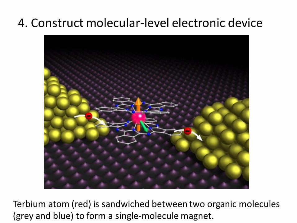
Atomic Force Microscope (AFM)
1986 --- Binnig, Quate and Gerber invented the first atomic force microscope

The structure of AFM
Feedback circuit
Position Sensing Part
Force Sensing Part
Position Sensing photodetector

The principle of AFM
When a tip is close to sample,
typically two forces operate:
Coulombic and van der Waals
interactions.
Coulombic Interaction: strong, short range
repulsive force between tip and sample.
This repulsion increases as the distance
decreases.
Van der Waals interactions: long range attractive force, which become
obvious at distance of down to 10 nm.
The combination of these interactions
results in a force-distance curve

•As tip is brought towards
the sample, van der Waals
forces cause attraction.
• As tip gets closer to the
sample this attraction
increases.
•However at very small
separations the repulsive
coulombic force becomes
dominant. The repulsive
force causes the cantilever
to bend when the tip is
getting closer to the
surface.

The manipulation of AFM
Constant-height scan
• Two scanning processes (contact mode):
Constant-force scan

• Three AFM imaging modes:
• 1. Contact AFM
• < 0.5 nm probe-surface separation
• 2. Tapping mode AFM
• 0.5-2 nm probe-surface separation
• 3. Non-contact AFM
• 0.1-10 nm probe-surface separation

• 1. Contact AFM
•tip contacts the sample
surface.
•The photo detector monitors
the changing of cantilever
deflection and the force is
calculated using Hooke’s law:
•The feedback circuit adjusts the probe height to maintain a constant
force and deflection on the cantilever, i.e. deflection setpoint.
F = − k x (F = force, k = spring constant, x = cantilever deflection)
Constant-force scan

• 2. Tapping mode AFM (Intermittent contact )
•cantilever oscillates at (or
slightly below) its resonant
frequency. Oscillation
amplitude ranges in 20-100
nm. Tip lightly touch
(“taps”) on sample surface
during scanning.
•Oscillation decreases when tip is closer to surface. Hence changes of
oscillation amplitude are used for measuring tip/surface separation.
Feedback circuit adjusts probe height to maintain a constant amplitude
of oscillation. i.e. the amplitude setpoint. Constant-height scan
• Resonant frequency of cantilever dependent on tip/surface separation.

Tapping mode in air:
A small piezoelectric crystal on AFM tip holder makes the cantilever oscillate up and down.
Tapping mode in liquids:
Tapping mode operation in liquids is a very useful tool for biologists.

• 3. Non-contact AFM
• cantilever oscillate near sample
surface, but does not contact it.
Oscillation is at slightly above
resonant frequency. Van der Waals
force decrease resonant frequency.
This decrease of resonant
frequency causes oscillation
amplitude to decrease.
•Normally adsorbed fluidic layer is much thicker than the dominant
region of van der Waals force - probe is either out of range of van der
Waals force, or becomes trapped in fluidic layer. Therefore non-
contact mode AFM works best under ultra-high vacuum conditions.

The Properties of the different operation modes in AFM.

Advantage Disadvantage
Contact Mode
- High scan speeds - “Atomic resolution” possible - Easier scanning of rough
samples with large changes in vertical topography.
• Lateral forces distort image • Combination of forces reduces spatial resolution and cause damage to soft samples.
Tapping Mode
- High lateral resolution (1 to 5 nm). - Lower forces, less damage to soft samples in air. - Almost no lateral forces.
• Slower scan speed than contact mode
Non-contact Mode
- Both normal and lateral forces are minimised, good for measuring very soft samples
- Can get atomic resolution in UHV environment
• Slower scan speed than tapping and contact modes •Lower lateral resolution, limited by tip-sample separation. •Usually only applicable in extremely hydrophobic samples with a minimium fluidic layer.
Advantages and Disadvantages of AFM Modes

• 1. Imaging
The application of AFM
AFM 3D image of a detail of the free surface of an artificial pattern
The figure illustrates 800 nm wide and 10 nm high Pd/Fe/Pd thin film dots fabricated using electron lithography.

NCAFM image of the Ge/Si(105) surface, 4.2 nm x 4.2 nm
PMMA spheres scanning range 45x45 μm
AFM image of human plasma sample (fibrinogen)

• 2. Measuring forces (and mechanical properties) at nanoscale
Illustration of an AFM tip measuring the force to move a cobalt atom on a crystalline surface. (Credit: Image courtesy of IBM) http://www.youtube.com/watch?v=BUq2bQkL1zo

Single-molecule force microscope uses a target molecule at AFM tip end to probe surface molecules with a strong attractive force. Force measurements are mapped as an image.

• 3. As a nanoscale tool
bending, cutting and extracting soft materials (Polymers, DNA, nanotubes), at nano-scale
grab and hold a nanoparticle in a position
Manipulating nanotube on Si substrate. AFM tip creates Greek letter "theta" from a 2.5 μm long nanotube

A single nanotube (red) on an insulating substrate (SiO2, green) is manipulated in a few steps onto a W film thin wire (blue), finally stretched across an tungsten oxide barrier (yellow).

Advantages :
1) high-resolution 3-D surface images
2) not require special sample treatments (no sample's destruction)
3) Usually not require vacuum (operate both in air and liquid);
4) could be used for organic materials
Disadvantages:
1) image size is much smaller than that of electron microscopes;
2) slow scanning rate, unlike an electron microscope which
does it in almost real-time.
3) tip convolution -- not true sample topography
4) expensive tips
The advantage and disadvantage of AFM

Tip convolution----Tip Related Artifacts
protrusions (dots) appear
wider, depressions (pores) appear narrower than the reality.

AFM Section Analysis of the nano-discs, the average height and size of
the nano-discs are approximately 1.5 and 80 nm, respectively.

AFM Section Analysis of the nano-hemisphere. To accurately reflect the shape
of the nanoparticles, we used the same dimension scale for the horizontal and
vertical coordinates. The average height and base diameter of the nano-
hemispheres are approximately 35-40 and 75 nm, respectively.

AFM Section Analysis of the nano-hemiellipsoids. To accurately reflect the shape
of the nanoparticles, we used the same dimension scale for the horizontal and
vertical coordinates. The average height and base diameter of the nano-
hemiellipsoids are approximately 50-55 and 65 nm, respectively.

AFM Section Analysis of the nano-conics. To accurately reflect the shape of the
nanoparticles, we used the same dimension scale for the horizontal and vertical
coordinates. The average height and base diameter of the nano-conics are
approximately 55-60 and 60 nm, respectively.

Thank you and have a nice day!