Technical specification for Small Form Factor Pluggable (SFP)lason/SFP/TRX100007/SCP6Gx8c.pdf ·...
18
Specification: TS-S08D026C September, 2008 (SCP6G28/SCP6G08-GL) 1 / 18 Technical specification for Small Form Factor Pluggable (SFP) OC-48 (2488.32Mbps) Sumitomo Part Number Function SCP6G28-GL-# W E SR, 1310nm, 2km SCP6G08-GL-# W E IR-1, 1310nm, 15km Sumitomo Electric reserves the right to make changes in this specification without prior notice. Sumitomo Electric Industries, Ltd. and ExceLight Communications, Inc. have been granted license to the following patents under a license agreement with Finisar corporation: US5,019,769, US6,439,918 B1 ---------------------------------------------------------------------------- #Safety Precaution Symbols This specification uses various picture symbols to prevent possible injury to operator or other persons or damage to properties for appropriate use of the product. The symbols and definitions are as shown below. Be sure to be familiar with these symbols before reading this specification. Caution Wrong operation without following this instruction may lead to human injury or property damage. ! ! Warning Wrong operation without following this instruction may lead to human death or serious injury. ! ! Examples of picture symbols indicates prohibition of actions. Action details are explained thereafter. indicates compulsory actions or instructions. Action details are explained thereafter. !
Transcript of Technical specification for Small Form Factor Pluggable (SFP)lason/SFP/TRX100007/SCP6Gx8c.pdf ·...

Specification: TS-S08D026C September, 2008
(SCP6G28/SCP6G08-GL) 1 / 18
TTeecchhnniiccaall ssppeecciiffiiccaattiioonn ffoorr
SSmmaallll FFoorrmm FFaaccttoorr PPlluuggggaabbllee ((SSFFPP))
OC-48 (2488.32Mbps)
Sumitomo Part Number Function
SCP6G28-GL-# W E SR, 1310nm, 2km
SCP6G08-GL-# W E IR-1, 1310nm, 15km
Sumitomo Electric reserves the right to make changes in this specification without prior notice. Sumitomo Electric Industries, Ltd. and ExceLight Communications, Inc. have been granted license to the
following patents under a license agreement with Finisar corporation: US5,019,769, US6,439,918 B1
- - - - - - - - - - - - - - - - - - - - - - - - - - - - - - - - - - - - - - - - - - - - - - - - - - - - - - - - - - - - - - - - - - - - - - - - - - - - #Safety Precaution Symbols This specification uses various picture symbols to prevent possible injury to operator or other persons or damage to properties for appropriate use of the product. The symbols and definitions are as shown below. Be sure to be familiar with these symbols before reading this specification.
Caution Wrong operation without following this instruction may lead to human injury or property damage.!!
Warning Wrong operation without following this instruction may lead to human death or serious injury.!! Examples of picture symbols indicates prohibition of actions. Action details are explained thereafter.
indicates compulsory actions or instructions. Action details are explained thereafter.
!

Specification: TS-S08D026C September, 2008
(SCP6G28/SCP6G08-GL) 2 / 18
1 General Features and applications of SCP6G28/SCP6G08 are listed below. Features
* RoHS-6 Compliant. * Compliant with SFP MSA. * SFF-8472 rev.9 compliant diagnostic monitoring implemented. * Power Supply Voltage Single +3.3V * Compact Package Size 57.5 X 13.9 X 8.6 mm * Electrical Interface AC coupled for DATA, LVTTL for Tx Disable and open collector output for
LOS and Tx Fault. Circuit ground is internally isolated from frame ground. * Connector Interface LC Duplex * Serial ID Functionality * Alarm and Warning Flags * Bail type Actuator
2 Block diagram
100LaserDriver
AutomaticPower
Controller
10k
4.7k – 10k
LD MonitorPD TD+
TD-
TxDisable
LOS
PostAmplifier 100
RD+
RD-Pre
Amplifier
PD
EEPROM
MOD- DEF0
SFP module Host board
150
MOD- DEF1MOD- DEF2
4.7k – 10k
4.7k – 10k
TxFault
Diagnostic monitor
TemperatureSupply voltage
Tx bias currentTx output power
Rx received power
Transmitter
Receiver
EEPROM
Figure 1. Block diagram
Caution!Do not disassemble this product. Otherwise, failure, electrical shock, overheating or fire may occur.
Caution!!Do not disassemble this product. Otherwise, failure, electrical shock, overheating or fire may occur.

Specification: TS-S08D026C September, 2008
(SCP6G28/SCP6G08-GL) 3 / 18
3 Package dimensions
Bail color is blue.
Note1 All Dimensions in mm
Note2 Dimensions with parentheses indicate the bail and latch release position
Figure 2. Package dimensions
Specification: TS-S08D026C September, 2008
(SCP6G28/SCP6G08-GL) 4 / 18
VeeT
VeeT
VeeR
VeeR
TD-
TD+
RD+
RD-
VccT
VccR
VeeT
VeeR
TXFault
MOD-DEF(2)
MOD-DEF(1)
MOD-DEF(0)
NUC
LOS
1
2
3
4
5
6
7
8
9
10
20
19
18
17
16
15
14
13
12
11
TowardsASIC
TowardsBezel
TX Disable
VeeR
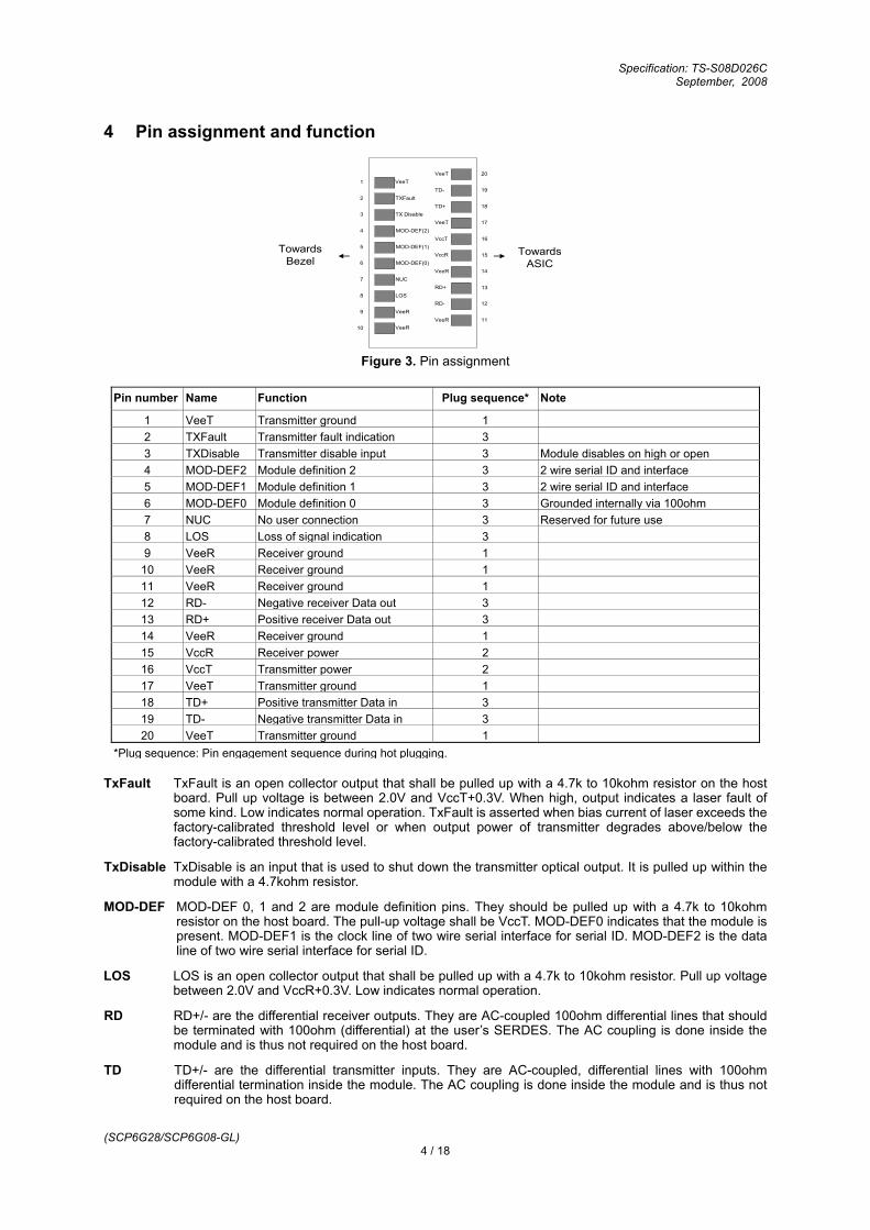
4 Pin assignment and function
Figure 3. Pin assignment
Pin number Name Function Plug sequence* Note
1 VeeT Transmitter ground 12 TXFault Transmitter fault indication 33 TXDisable Transmitter disable input 3 Module disables on high or open 4 MOD-DEF2 Module definition 2 3 2 wire serial ID and interface 5 MOD-DEF1 Module definition 1 3 2 wire serial ID and interface 6 MOD-DEF0 Module definition 0 3 Grounded internally via 100ohm 7 NUC No user connection 3 Reserved for future use 8 LOS Loss of signal indication 39 VeeR Receiver ground 1
10 VeeR Receiver ground 111 VeeR Receiver ground 112 RD- Negative receiver Data out 313 RD+ Positive receiver Data out 314 VeeR Receiver ground 115 VccR Receiver power 216 VccT Transmitter power 217 VeeT Transmitter ground 118 TD+ Positive transmitter Data in 319 TD- Negative transmitter Data in 320 VeeT Transmitter ground 1
*Plug sequence: Pin engagement sequence during hot plugging. TxFault TxFault is an open collector output that shall be pulled up with a 4.7k to 10kohm resistor on the host
board. Pull up voltage is between 2.0V and VccT+0.3V. When high, output indicates a laser fault of some kind. Low indicates normal operation. TxFault is asserted when bias current of laser exceeds the factory-calibrated threshold level or when output power of transmitter degrades above/below the factory-calibrated threshold level.
TxDisable TxDisable is an input that is used to shut down the transmitter optical output. It is pulled up within the module with a 4.7kohm resistor.
MOD-DEF MOD-DEF 0, 1 and 2 are module definition pins. They should be pulled up with a 4.7k to 10kohm resistor on the host board. The pull-up voltage shall be VccT. MOD-DEF0 indicates that the module is present. MOD-DEF1 is the clock line of two wire serial interface for serial ID. MOD-DEF2 is the data line of two wire serial interface for serial ID.
LOS LOS is an open collector output that shall be pulled up with a 4.7k to 10kohm resistor. Pull up voltage between 2.0V and VccR+0.3V. Low indicates normal operation.
RD RD+/- are the differential receiver outputs. They are AC-coupled 100ohm differential lines that should be terminated with 100ohm (differential) at the user’s SERDES. The AC coupling is done inside the module and is thus not required on the host board.
TD TD+/- are the differential transmitter inputs. They are AC-coupled, differential lines with 100ohm differential termination inside the module. The AC coupling is done inside the module and is thus not required on the host board.

Specification: TS-S08D026C September, 2008
(SCP6G28/SCP6G08-GL) 5 / 18
Figure 4 SFP host board mechanical layout
Figure 5 Recommended bezel design
Specification: TS-S08D026C September, 2008
(SCP6G28/SCP6G08-GL) 6 / 18
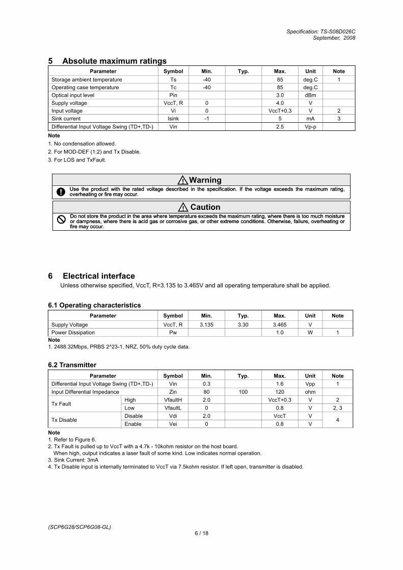
5 Absolute maximum ratings Parameter Symbol Min. Typ. Max. Unit Note
Storage ambient temperature Ts -40 85 deg.C 1 Operating case temperature Tc -40 85 deg.C Optical input level Pin 3.0 dBm Supply voltage VccT, R 0 4.0 V Input voltage Vi 0 VccT+0.3 V 2 Sink current Isink -1 5 mA 3 Differential Input Voltage Swing (TD+,TD-) Vin 2.5 Vp-p
Note 1. No condensation allowed. 2. For MOD-DEF (1:2) and Tx Disable. 3. For LOS and TxFault.
!Warning!
Use the product with the rated voltage described in the specification. If the voltage exceeds the maximum rating, overheating or fire may occur.!
Warning!!Use the product with the rated voltage described in the specification. If the voltage exceeds the maximum rating, overheating or fire may occur.
Caution!Do not store the product in the area where temperature exceeds the maximum rating, where there is too much moisture or dampness, where there is acid gas or corrosive gas, or other extreme conditions. Otherwise, failure, overheating or fire may occur.
Caution!!Do not store the product in the area where temperature exceeds the maximum rating, where there is too much moisture or dampness, where there is acid gas or corrosive gas, or other extreme conditions. Otherwise, failure, overheating or fire may occur.
6 Electrical interface
Unless otherwise specified, VccT, R=3.135 to 3.465V and all operating temperature shall be applied.
6.1 Operating characteristics Parameter Symbol Min. Typ. Max. Unit Note
Supply Voltage VccT, R 3.135 3.30 3.465 V Power Dissipation Pw 1.0 W 1
Note 1. 2488.32Mbps, PRBS 2^23-1, NRZ, 50% duty cycle data.
6.2 Transmitter Parameter Symbol Min. Typ. Max. Unit Note
Differential Input Voltage Swing (TD+,TD-) Vin 0.3 1.6 Vpp 1 Input Differential Impedance Zin 80 100 120 ohm
High VfaultH 2.0 VccT+0.3 V 2 Tx Fault
Low VfaultL 0 0.8 V 2, 3 Disable Vdi 2.0 VccT V
Tx Disable Enable Vei 0 0.8 V
4
Note 1. Refer to Figure 6. 2. Tx Fault is pulled up to VccT with a 4.7k - 10kohm resistor on the host board. When high, output indicates a laser fault of some kind. Low indicates normal operation. 3. Sink Current: 3mA 4. Tx Disable input is internally terminated to VccT via 7.5kohm resistor. If left open, transmitter is disabled.
Specification: TS-S08D026C September, 2008
(SCP6G28/SCP6G08-GL) 7 / 18
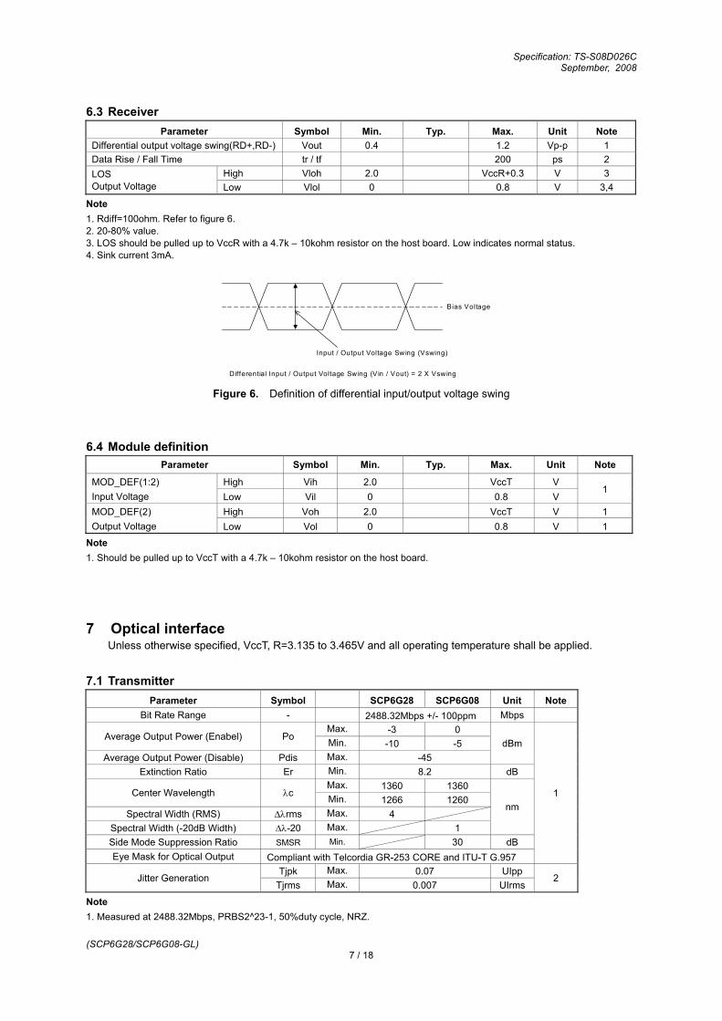
6.3 Receiver Parameter Symbol Min. Typ. Max. Unit Note
Differential output voltage swing(RD+,RD-) Vout 0.4 1.2 Vp-p 1 Data Rise / Fall Time tr / tf 200 ps 2
High Vloh 2.0 VccR+0.3 V 3 LOS Output Voltage Low Vlol 0 0.8 V 3,4
Note 1. Rdiff=100ohm. Refer to figure 6. 2. 20-80% value. 3. LOS should be pulled up to VccR with a 4.7k – 10kohm resistor on the host board. Low indicates normal status. 4. Sink current 3mA.
Figure 6. Definition of differential input/output voltage swing
6.4 Module definition Parameter Symbol Min. Typ. Max. Unit Note
High Vih 2.0 VccT V MOD_DEF(1:2) Input Voltage Low Vil 0 0.8 V
1
High Voh 2.0 VccT V 1 MOD_DEF(2) Output Voltage Low Vol 0 0.8 V 1
Note 1. Should be pulled up to VccT with a 4.7k – 10kohm resistor on the host board. 7 Optical interface
Unless otherwise specified, VccT, R=3.135 to 3.465V and all operating temperature shall be applied.
7.1 Transmitter Parameter Symbol SCP6G28 SCP6G08 Unit Note
Bit Rate Range - 2488.32Mbps +/- 100ppm Mbps Max. -3 0
Average Output Power (Enabel) Po Min. -10 -5 Average Output Power (Disable) Pdis Max. -45
dBm
Extinction Ratio Er Min. 8.2 dB Max. 1360 1360
Center Wavelength λc Min. 1266 1260 Spectral Width (RMS) Δλrms Max. 4
Spectral Width (-20dB Width) Δλ-20 Max. 1
nm
Side Mode Suppression Ratio SMSR Min. 30 dB Eye Mask for Optical Output Compliant with Telcordia GR-253 CORE and ITU-T G.957
1
Tjpk Max. 0.07 UIpp Jitter Generation
Tjrms Max. 0.007 UIrms 2
Note 1. Measured at 2488.32Mbps, PRBS2^23-1, 50%duty cycle, NRZ.
Bias Voltage
Input / Output Voltage Swing (Vswing)
D ifferential Input / Output Voltage Swing (Vin / Vout) = 2 X Vswing

Specification: TS-S08D026C September, 2008
(SCP6G28/SCP6G08-GL) 8 / 18
2. SONET OC-48c data pattern filled with a 2^23-1, PRBS payload. Measured with a band pass filter having a high-pass cutoff frequency of 12kHz and a low-pass cutoff frequency of 20MHz.
Figure 7. Optical Pulse Mask with Fourth Order Bessel Thomson Filter Specified in ITU-T G.957
Warning!Do not look at the laser beam projection area (e.g. end of optical connector) with naked eyes or through optical equipment while the power is supplied to this product. Otherwise, your eyes may be injured.
Warning!!Do not look at the laser beam projection area (e.g. end of optical connector) with naked eyes or through optical equipment while the power is supplied to this product. Otherwise, your eyes may be injured.
7.2 Receiver
Parameter Symbol SCP6G28 SCP6G08 Unit Note
Bit Rate Range - 2488.32Mbps +/- 100ppm Mbps Max. 1580
Center Wavelength - Min. 1260
nm
Overload Pmax Min. +0 Minimum Sensitivity Pmin Max. -19
1, 2
Max. -19.5 LOS Activation Level PLa
Min. -35 Max. -19
LOS Deactivation Level PLd Min. -34.5
dBm
Max. 6.0 LOS Hysteresis Phys
Min. 0.5
2
Optical Reflectance REFr Max -27 dB
Note 1. BER = 1E-10. 2. Measured at 2488.32Mbps, PRBS2^23-1, NRZ 7.3 Transceiver timing characteristics
Parameter Symbol Min. Typ. Max. Unit Note TxDisable assert time t_off 10 us 1 TxDisable negate time t_on 1 ms 2 Time to initialize t_init 300 ms 3 TxFault assert time t_fault 100 us 4 TxDisable to reset t_reset 10 us 5 LOS assert time t_loss_on 100 us 6 LOS de-assert time t_loss_off 100 us 7 Serial ID clock rate - 100 kHz
1.25
1.00
0.75
0.25
0
-0.25
0.20UI
Time (UI)0 1.0
Nor
mal
ized
Am
plitu
de
Logic " 1 "
Logic " 0 "
Specification: TS-S08D026C September, 2008
(SCP6G28/SCP6G08-GL) 9 / 18
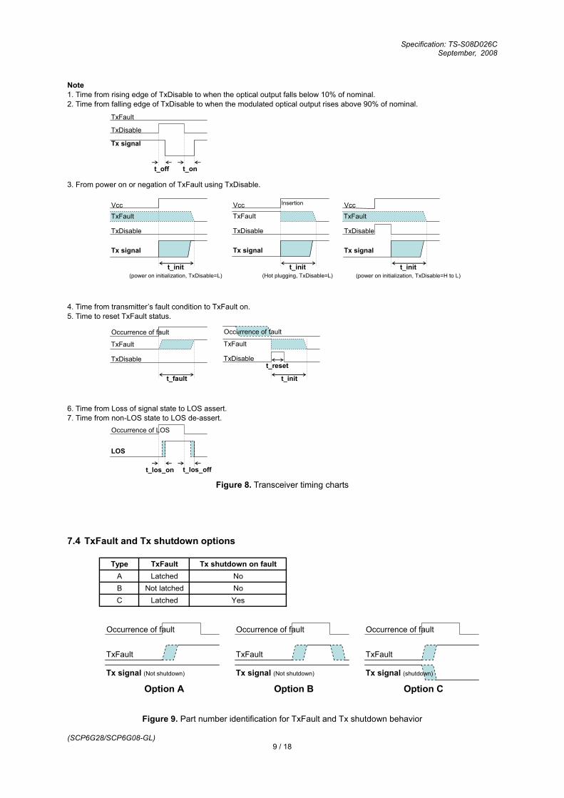
Note 1. Time from rising edge of TxDisable to when the optical output falls below 10% of nominal. 2. Time from falling edge of TxDisable to when the modulated optical output rises above 90% of nominal.
TxFault
TxDisable
Tx signal
t_off t_on 3. From power on or negation of TxFault using TxDisable.
TxFault
TxDisable
Tx signal
t_init(power on initialization, TxDisable=L)
VccTxFault
TxDisable
Tx signal
t_init(Hot plugging, TxDisable=L)
Vcc Insertion
TxDisable
Tx signal
t_init(power on initialization, TxDisable=H to L)
VccTxFault
4. Time from transmitter’s fault condition to TxFault on. 5. Time to reset TxFault status.
TxFault
TxDisable
t_fault
Occurrence of fault
TxFault
TxDisable
t_init
Occurrence of fault
t_reset
6. Time from Loss of signal state to LOS assert. 7. Time from non-LOS state to LOS de-assert.
Occurrence of LOS
LOS
t_los_on t_los_off Figure 8. Transceiver timing charts
7.4 TxFault and Tx shutdown options
Figure 9. Part number identification for TxFault and Tx shutdown behavior
TxFault
Tx signal (Not shutdown)
Occurrence of fault
Option A
TxFault
Tx signal (Not shutdown)
Occurrence of fault
Option B
TxFault
Tx signal (shutdown)
Occurrence of fault
Option C
Type TxFault Tx shutdown on faultA Latched NoB Not latched NoC Latched Yes

Specification: TS-S08D026C September, 2008
(SCP6G28/SCP6G08-GL) 10 / 18
8 EEPROM memory contents The data can be read using the 2-wire serial CMOS EEPROM protocol of the Atmel AT24C01A or equivalent.
1010000X(A0h) 1010001X(A2h)
0 Serial ID (96bytes) 0 Alarm and warning thresholdsection 8.1 (56bytes)
5556 Cal constants (40bytes)
95 9596 Vendor specific (32bytes) 96 Realtime diagnostic interface
(24bytes)section 8.2
119127 120 Vendor specific (136bytes)128 Reserved (128bytes)
255 255
Figure 10. Digital diagnostic memory map

Specification: TS-S08D026C September, 2008
(SCP6G28/SCP6G08-GL) 11 / 18
8.1. Serial ID (A0h)
Address Name of field Hex ASCII Description Address Name of field Hex ASCII Description
0 Identifier 03 SFP Transceiver 64 001 Ext. Identifier 04 65 1A2 Connector 07 LC Connector 66 BR, max 003 00 67 BR, min 004 00 68 Year5 00 69 Month6 00 707 00 718 00 729 00 7310 00 7411 Encoding 05 SONET Scrambled 7512 BR, Nominal 19 2488.32Mbps 7613 Reserved 00 7714 Length(9um) - km 7815 Length (9um) 7916 Length (50um) 00 8017 Length (62.5um) 00 8118 Length (Copper) 00 8219 Reserved 00 8320 53 S 8421 75 u 8522 6D m 8623 69 i 8724 74 t 8825 6F o 8926 6D m 9027 6F o 9128 45 E 92 Diagnostic Monitoring Type 58 Note629 6C l 93 Enhanced Options F0 Note730 65 e 94 SFF-8472 Compliance 01 Diagnostics31 63 c 95 CC_EXT Note532 74 t33 72 r 96 2034 69 i 97 2035 63 c 98 2036 Reserved 00 99 2037 00 100 2038 00 101 2039 5F 102 2040 53 S 103 2041 43 C 104 2042 50 P 105 2043 36 6 106 2044 47 G 107 2045 32/30 2/0 108 2046 38 8 109 2047 2D - 110 2048 47 G 111 2049 4C L 112 2050 2D - 113 2051 41/42/43 A/B/C TxFault Type 114 2052 57 W Temperature Range 115 2053 45 E Diagnostics 116 2054 20 117 2055 20 118 2056 41 to 5A A to Z Variable 119 2057 20 120 2058 20 121 2059 20 122 2060 123 2061 124 2062 Reserved 00 125 2063 CC_BASE Note2 126 20
127 20
Note4
Vendor rev
Wavelength
Vendor PN
Vendor OUI
Read-only
Vendor name
Date code
Note1
VENDOR SPECIFIC ID FIELDS
Transceiver
BASE ID FIELDS EXTENDED ID FIELDS
Options
Vendor SN Note3
Note1

Specification: TS-S08D026C September, 2008
(SCP6G28/SCP6G08-GL) 12 / 18
Note 1. Refer to the section 8-2. 2. Address 63 is a checksum of bytes 0 to 62. 3. Address 68 to 83 is vendor’s serial number area. 4. Address 84 to 91 is date-code. 5. Address 95 is a checksum of bytes 64 to 94. 6. Diagnostic monitoring types are listed below.
Address Bit Status Description 92 7 0 Reserved for legacy diagnostic implementations. 92 6 1 Digital diagnostic monitoring is implemented. 92 5 0 92 4 1
externally calibrated
92 3 1 Receiver power measurement type. 1=Average power. 92 2 0 Address change is not required. 92 1 0 Reserved 92 0 0 Reserved
7. Enhanced options are listed below.
Address Bit Status Description 93 7 1 Alarm/warning flags implemented for all monitored quantities 93 6 1 Soft TxDisable control is implemented. 93 5 1 Soft TxFault monitoring is implemented. 93 4 1 Soft RxLOS monitoring is implemented. 93 3 0 Soft rate-select control and monitoring is not implemented. 93 2 0 Reserved 93 1 0 Reserved 93 0 0 Reserved
8.2. SCP6G28/6G08-xWE EEPROM Information (Transceiver Code etc)
SCP6G28 SCP6G08Hex Hex
3 00 004 01 12 01:SR, 12:IR-1 , 0A:IR-25 00 006 00 007 00 008 00 009 00 0010 00 0014 Length(9um) - km 02 0F 02:2km, 0F:15km, 0F:15km15 Length (9um) 14 96 14:20*100m, 96:150*100m, 96:150*100m60 05 0561 1E 1E
Address Name of field
Wavelength 051E: 1310nm, 060E: 1550nm
Description
Transceiver

Specification: TS-S08D026C September, 2008
(SCP6G28/SCP6G08-GL) 13 / 18
8.3 Real-time diagnostics (A2h) Setting of bit 6, address 92 means digital diagnostic monitoring is implemented. Two calibration options are possible. If bit 5 of address 92,”Internally calibrated”, is set, the transceiver directly reports calibrated values in units of current, power etc. If bit 4, “Externally calibrated”, is set, the reported values are A/D counts which must be converted to real world units using calibration values read using 2 wire serial address 1010001X(A2h) from bytes 55 to 95. Monitoring range and accuracy are described in section 8.4.
Address Bit Name Description
96 MSB 97 LSB
Temperature (TAD) Junction temperature of the point illustrated in section 3. 16-bit signed 2’s complement value. See Note 1 and 6.
98 MSB 99 LSB
Vcc (VAD) Internally measured supply voltage “VccT” in a module. Unsigned 16-bit value. See Note 2 and 6.
100 MSB 101 LSB
Tx bias current (IAD) Unsigned 16-bit value. See Note 3 and 6.
102 MSB 103 LSB
Tx power (TPAD) Measured TX output power. Unsigned 16-bit value. See Note 4 and 6.
104 MSB 105 LSB
Rx power (RPAD) Measured RX received power. Unsigned 16-bit value. 1digit=0.1uW. See Note 5 and 6.
106 - - Reserved 107 - - Reserved 108 - - Reserved 109 - - Reserved
Note
1. Temperature (1/256deg.C/digit) T = Tslope * TAD + Toffset (Ext. cal.) 2. Vcc (100uV/digit) V = Vslope * VAD + Voffset (Ext. cal.) 3. TX bias current (2uA/digit) I = Islope * IAD + Ioffset (Ext. cal.) 4. TX power (0.1uW/digit) TP = TPslope * TPAD + TPoffset (Ext. cal.) 5. RX power (0.1uW/digit) RP = RP4*RPAD
4+RP3*RPAD3+RP2*RPAD
2+RP1*RPAD+RP0 (Ext. cal.) 6. Calibration constants(A2h) are listed below.
Address Bytes Name Description
56:59 4 RP4 Single precision floating-point calibration data. Byte 56 is MSB.60:63 4 PR3 Single precision floating-point calibration data. Byte 60 is MSB.64:67 4 PR2 Single precision floating-point calibration data. Byte 64 is MSB.68:71 4 PR1 Single precision floating-point calibration data. Byte 68 is MSB.72:75 4 RP0 Single precision floating-point calibration data. Byte 72 is MSB.76:77 2 Islope Unsigned fixed-point calibration data. Byte 76 is MSB. 78:79 2 Ioffset 16-bit signed 2’s complement calibration data. Byte 78 is MSB.80:81 2 TPslope Unsigned fixed-point calibration data. Byte 80 is MSB. 82:83 2 TPoffset 16-bit signed 2’s complement calibration data. Byte 82 is MSB.84:85 2 Tslope Unsigned fixed-point calibration data. Byte 84 is MSB. 86:87 2 Toffset 16-bit signed 2’s complement calibration data. Byte 86 is MSB.88:89 2 Vslope Unsigned fixed-point calibration data. Byte 88 is MSB. 90:91 2 Voffset 16-bit signed 2’s complement calibration data. Byte 90 is MSB.92:94 3 - Reserved
95 1 - Checksum. Low order 8 bits of the sum at data address 0 to 94.

Specification: TS-S08D026C September, 2008
(SCP6G28/SCP6G08-GL) 14 / 18
8.4 A/D accuracy and monitoring range
Monitoring range Parameter Accuracy Min. Max.
Unit Note
Temperature +/- 3deg.C -40 85 deg.C 1 Vcc +/- 3% 3.135 3.465 V Tx bias current +/- 10% 1 60 mA 2
-10 -3 SCP6G28 Tx power +/- 3dB
-5 +0 dBm
SCP6G08 Rx Power Note3 +/-3dB -22 +0 dBm
Note 1. Junction temperature. Specified at Vcc=3.3V. 2. Specified by nominal value. 3. At specified transmitter wavelength. 8.5 Optional status bit(A2h)
Address Bit Name Description
110 0 Data ready bar Indicates transceiver has achieved power up and data is ready. Bit remains high until data is ready to be read.
8.6 Alarm and Warning Flags(A2h)
Address Bit Name Description
7 Temp High Alarm Set when temperature exceeds high alarm level. 6 Temp Low Alarm Set when temperature is below low alarm level. 5 Vcc High Alarm Set when measured internal voltage exceeds high alarm level.4 Vcc Low Alarm Set when measured internal voltage is below low alarm level. 3 Tx bias High Alarm Set when TX bias current exceeds high alarm level. 2 Tx bias Low Alarm Set when TX bias current is below low alarm level. 1 Tx power High Alarm Set when TX output power exceeds high alarm level.
112
0 Tx power Low Alarm Set when TX output power is below low alarm level. 7 RX power High Alarm Set when received power exceeds high alarm level. 6 RX power Low Alarm Set when received power is below low alarm level. 113
5:0 Reserved 114 7:0 Reserved 115 7:0 Reserved
7 Temp High Warning Set when temperature exceeds high warning level. 6 Temp Low Warning Set when temperature is below low warning level. 5 Vcc High Warning Set when measured internal voltage exceeds high warning level.4 Vcc Low Warning Set when measured internal voltage is below low warning level.3 Tx bias High Warning Set when TX bias current exceeds high warning level. 2 Tx bias Low Warning Set when TX bias current is below low warning level. 1 Tx power High Warning Set when TX output power exceeds high warning level.
116
0 Tx power Low Warning Set when TX output power is below low warning level. 7 RX power High Warning Set when received power exceeds high warning level. 6 RX power Low Warning Set when received power is below low warning level. 117
5:0 Reserved 118 7:0 Reserved 119 7:0 Reserved
Specification: TS-S08D026C September, 2008
(SCP6G28/SCP6G08-GL) 15 / 18
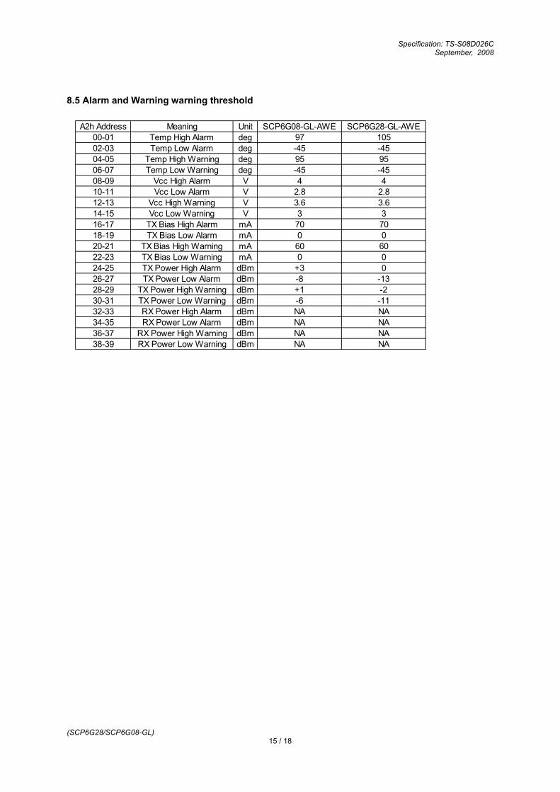
8.5 Alarm and Warning warning threshold
A2h Address Meaning Unit SCP6G08-GL-AWE SCP6G28-GL-AWE
00-01 Temp High Alarm deg 97 10502-03 Temp Low Alarm deg -45 -4504-05 Temp High Warning deg 95 9506-07 Temp Low Warning deg -45 -4508-09 Vcc High Alarm V 4 410-11 Vcc Low Alarm V 2.8 2.812-13 Vcc High Warning V 3.6 3.614-15 Vcc Low Warning V 3 316-17 TX Bias High Alarm mA 70 7018-19 TX Bias Low Alarm mA 0 020-21 TX Bias High Warning mA 60 6022-23 TX Bias Low Warning mA 0 024-25 TX Power High Alarm dBm +3 026-27 TX Power Low Alarm dBm -8 -1328-29 TX Power High Warning dBm +1 -230-31 TX Power Low Warning dBm -6 -1132-33 RX Power High Alarm dBm NA NA34-35 RX Power Low Alarm dBm NA NA36-37 RX Power High Warning dBm NA NA38-39 RX Power Low Warning dBm NA NA

Specification: TS-S08D026C September, 2008
(SCP6G28/SCP6G08-GL) 16 / 18
9 Recommended interface circuit
TRANSMIT DATA
100Ω
RECEIVE DATA
SFPMODULE
TD+
TD-
RD+
RD-
MOD- DEF (0)
MOD- DEF (1)
MOD- DEF (2)
100Ω
Vcc
4.7k to
TX Fault
TX Disable
4.7k to10kΩ
LOS
4.7k to
VccT
Ω
HOSTBOARD
10kΩ
10kΩ
Vcc
Vcc
EEPROM
50Ω lineFG
DiagnosticMonitor
10k
150
Figure 11. Recommended interface circuit
Figure 12. Recommended supply filtering network
VccT
VccR
SFP Module
1uH
0.1uF
0.1uF 10uF
1uH
0.1uF 10uF
3.3V
VeeT
VeeR

Specification: TS-S08D026C September, 2008
(SCP6G28/SCP6G08-GL) 17 / 18
GR-468-CORE Issue 1, December 1998 Laser module
LTPD SS C
Mechanical shock MIL-STD-883Method 2002
5 times/axis1,500G, 0.5ms 20 11 0
Vibration MIL-STD-883Method 2007
Cond. A 20G, 20 to 2,000Hz,4min/cy, 4cy/axis 20 11 0
Accel. aging (High temp.) (R)-4-53Section 5.18
85deg.C; rated power1,000h for pass/fail2,000 & 5,000h for info
- 2510
-
Low temp. storage -Minimum strage temperature1,000h for pass/fail2,000h for info
20 11 0
Temperature cycling Section 5.20-40 to 85deg.C500cy for pass/fail1,000cy for info
20-
1111
0-
Damp heat with biasMIL-STD-202Method 103 orIEC-60068-2-3
85deg.C/85%RH1,000h 20 11 0
Cyclic moisture resistance Section 5.23 - 20 11 0
Internal moisture MIL-STD-883Method 1018 Max. 5,000ppm water vapor 20 11 0
ESD threshold Section 5.22 - 6 -
SS; sample sizeC; maximum number of failure allowed to pass the test.
Sampling
Mechanical Integrity
Endurance
Special test
Heading Test Reference Conditions
10. RoHS COMPLIANCY Compliancy versus requirements contained inside the following reference document is guaranteed: ”Directive 2002/95/EC of 27 January 2003 on the restriction of the use of certain hazardous substances in electrical and electronic equipment: from official journal of European Union (European Parliament and of the Council). This product is Compliant at RoHS-6/6 level and Contains no leaded solders. 11 Reliability test program 12 Laser safety This product uses a semiconductor laser system and is a laser class 1 product acceptable FDA, complies with 21CFR 1040.10 and 1040.11. Also this product is a laser class 1 product acceptable IEC60825-1:2001.
Caution!!If this product is used under conditions not recommended in the specification or this product is used with unauthorized revision, classification for laser product safety standard is invalid. Classify the product again at your responsibility and tale appropriate actions.
13 Other precaution Under such a strong vibration environment as in automobile, the performance and reliability are not guaranteed. The governmental approval is required to export this product to other countries. To dispose of these components, the appropriate procedure should be taken to prevent illegal exportation. This module must be handled, used and disposed of according to your company’s safe working practice.
Operating transceiver products can have an outer package temperature exceeding 70degC. To reduce the risk of injury from burns, do not touch the transceiver module underany circumstances while it is operational. When installing or uninstalling products that have been operating, handle with extreme care.
WarningOperating transceiver products can have an outer package temperature exceeding 70degC. To reduce the risk of injury from burns, do not touch the transceiver module underany circumstances while it is operational. When installing or uninstalling products that have been operating, handle with extreme care.
WarningOperating transceiver products can have an outer package temperature exceeding 70degC. To reduce the risk of injury from burns, do not touch the transceiver module underany circumstances while it is operational. When installing or uninstalling products that have been operating, handle with extreme care.
Warning
Specification: TS-S08D026C September, 2008
(SCP6G28/SCP6G08-GL) 18 / 18
Warning!!Do not put this product or components of this product into your mouth. This product contains material harmful to health.
Caution!!Dispose this product or equipment including this product properly as industrial waste according to the regulations.
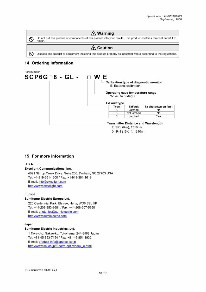
14 Ordering information Part number
SCP6G□8 - GL - □ W E Calibration type of diagnostic monitor E: External calibration Operating case temperature range W: -40 to 85degC TxFault type
Type TxFault Tx shutdown on faultA Latched No B Not latched No C Latched Yes
Transmitter Distance and Wavelength 2: SR (2Km), 1310nm 0: IR-1 (15Km), 1310nm 15 For more information U.S.A. Excelight Communications, Inc.
4021 Stirrup Creek Drive, Suite 200, Durham, NC 27703 USA Tel. +1-919-361-1600 / Fax. +1-919-361-1619 E-mail: [email protected] http://www.excelight.com
Europe Sumitomo Electric Europe Ltd.
220 Centennial Park, Elstree, Herts, WD6 3SL UK Tel. +44-208-953-8681 / Fax. +44-208-207-5950 E-mail: [email protected] http://www.sumielectric.com
Japan Sumitomo Electric Industries, Ltd.
1 Taya-cho, Sakae-ku, Yokohama, 244-8588 Japan Tel. +81-45-853-7154 / Fax. +81-45-851-1932 E-mail: [email protected] http://www.sei.co.jp/Electro-optic/index_e.html