TECHNICAL MANUAL - S100 Computers
130
THE WORLD'S fiRST . ... S ... 00 Single Board Computer TECHNICAL MANUAL for SUPER QUAD 12700·8 Knott Avenue. Garden Grove. CA 92641 TELE: (714) 891-4004 / TELEX: 678401 Tabirin
Transcript of TECHNICAL MANUAL - S100 Computers

THE WORLD'S fiRST . ...
S ... 00 Single Board Computer
TECHNICAL MANUAL
for
SUPER QUAD
12700·8 Knott Avenue. Garden Grove. CA 92641 TELE: (714) 891-4004 / TELEX: 678401 Tabirin

INTROoucrroN
ADVANCED DIGITAL CORPORATION is proud to introduce the SUPER QUAD.
The SUPER QUAD is a Z80 based single board caTlputer designed to be
a bus master in an SIOO bus system. The SUPER QUAD SOC has all the
hardware needed to run a single user CP 1M system or 2 user MP 1M system with up to 4 external floppy disk drives and an external
Centronics parallel interface printer all on one board.
The board also runs with TUROO-OOS tm.
The SUPER QUAD SBC contains:
1) Z-80A cpu (4 MHZ)
2) Floppy disk controller (up to 4 drives 8" or 5~")
3) 64K of dynamic merrory (16K bank selectible)
4) 2K or 4K of shadaN epran (2716 or 2732)
5) 2 serial ports (Z80A SIO opt. syncronous)
6) 2 12 bit parallel ports, (Z80A PIO)
one of which can be used
for SIOO vectored interrupts
7) Real time interrupt clock (Z80A CTC)
8) SIOO extended address Al6-A23
ONE YEAR WARRANTY.
*Note: Items 5 and 6 require external adaptation for RS-232 and
Centronics. The adapter boards are 2 .X 2" and are called
PS NET. They hoop up to the back of the main frame with
a DB-25 connector.
1

TABLE OF CONTENTS Page
introduction . . . . . . . . . . . . . . . . . . . . . . . . . . . . . . . . . . . . . . . . . . . . . . . . . . . 1
Table of Contents •••••••••••••••••••••••••••••••••••••••••••••• 2,3
1.0
2.0
Operation •••••••••••••••••••••••••••••••••••••• 1.1 Floppy disk •••••••••••••••••••••••••••• 1.2 64 K Dynamic Ram ••••••••••••• :- ••••••••• 1.3 Monitor Eprom •••••••••••••••••••••••••• 1.4 Serial Ports ••••••••••••••••••••••••••• 1.5 Parallel Ports ••••••••••••••••••••••• ~. 1.6 Real Time Clock •••••••••••••••••••••••• 1.7 5100 bus interface •••••••••••••••••••••
EPROM 2.1 2.2 2.3 2.4
and Monitor •••••••••••••••••••••••••••••• Enable I Disable software ••••••••••••••• Monitor Sign-on ••••••••••••••••••••••••• Monitor Commands ••••••••••••••••••••••• Cold boot loader program •••••••••••••••
4 4 5 5 5 6 6
7 7 8 8 9
3.0 Input / Output port assignments ••••••••••••••••• 10
4.0
5.0
6.0
Input / Output port description 11
4.1 SIO serial port channel A •••••••••••••• 11 4.2 SIO serial port channel B •••••••••••••• 11 4.3 PIO parallel port channel A •••••••••••• 11 4.4 PIO parallel port channel B ••••••.•••.• 11 4.5 Control ti~et Interrupt circuit ••••••• 11 4.6 Floppy Disk controller ••••••••••••••••• 11 4.7 Floppy disk control port ••••••••••••••• 12 4.8 Extended address port •••••••••••••••••• 13 4.9 On-board memory control port ••••••••••• 14
Jumper
Jumper 6.1 6.2 6.3 6.4 6.5 6.6 6.7 6.8 6.9 6.10
6.11 6.12
definitio11S •••••••••••••••••••••••••••••
descriptions •••••••••••••••••••••••••••• Jumper A - CPU clock rate •••••••••••••• Jumper B - SIO channel A clock ••••••••• Jumper C - SIO channel B clock ••••••••• Jumper D - Drive type selection •••••••• Jumper E - VIO I Jumper P - VIO / Jumper N - VII / Jumper M - VI2 / Jumper K - VI3 / Jumper J - VI4 /
PINT . . . . . . . . . . . . . . . . . . para1led bit D0 · . . . . . . paralled bit 01 · . . . . . . paralled bit D2 · . . . . . . paralled bit D3 · . . . . . . paralled bit D4 · ......
Jumper H - VIS / para1led bit D5 Jumper G - VI6 / paralled bit D6
2
15
15
16 16 17 18 18 18
18 19

7.0
8.0
6.13 6.14 6.15 6.16 6.17
Jumper F - VI7 / paralled bit D7 •••••.• 19 Jumper R - 2716 / 2732 •••••••••••••••.• 19 Jumper S - Floppy connector ••••••••••.• Jumper T - Memory Write Signal ••••••••• 20 Jumper layout ••••••••••••••••••••••••••• AA
Baud 7.1
Rate Switch ••••••••••••••••••••••••••••••• Switch Setting . . . . . . . . . . . . . . . . . . . . . . . . .
External Connector pin definitions •••••••••••.• 8.1 J1 - S10~ ~us •••••••••••••••••••••••••• 8.2 J2 - Parallel Port •••••••••••••••••••.• 8.3 J3 Floppy Disk controller ••••••••••.• 8.4 J4 Serial port channel A •••••••••••.• 8.5 J5 Serial port channel B •••••••••••••
21 21
22 22 23 24 25 25
9.0 Block Diagram ••••••••••••••••••••••••••••••.••• 26
10.0 Factory 10.1 10.2 10.3 10.4 10.5 10.6 10.7 10.8 10.9 10.9.1
Ins tall e d J urn per s ••••••••.•••••••••••.• 8 inch drive configuration ••••••••••••• 5.25 inch drive configuration •••••••••• Shugart 801 drive •••••••••••••••••••••• shugart 850 ••••••••••••••••••••••••••••• MP I d r i ve •••••••••••••••••••••••••••••• MFE model 7Q0 ••••••••••••••••••••••••••• TANDON SLIM LINE •••.•••••••••••••••••.• NEC model FDl160 •••• ~ •••••••••••••••••.• QUME Data Track 8 •••••••••••••••••••.•.• TANDON 5 1/4" ...•.......................
27
28 29
30
31
11.0 Appendex & Data sheets ••••••.••••.••••••••••••• 32 11.1 Appendex A - Z80A SIO / DART ••••••.•..• 11.2 Appendex B - Z80A PIO ••••••••••••••••.• 11.3 Appendex C - Z80A CTC •••••••••••••.••.• 11.4 Appendex D - Floppy Disk controller .•.• 11.4.1 WD l691,BR1941 ••••••••••••.•••••••••••.• 11.5 Appendex E - Z80A CPU •••••••••.•••••••• 11.6 Appendix F- FLOPPY ERROR CODE .•••••.•.• 11.8 Warranty ••••••••••••••••••••••••••••.•.• 11.9 Application notes:
Turbo-Dos app. notes .•• Additional memory boards ••.•.
11.10 Recomended additional 5-100 boards: Hard disk: morrow designs,konan,xcomp Memory: measurement systems,PCE Graphics: micro angelo Slave Processor: Advanced Digital, Musys corp.
12.0 Parts list
13.0 Schematic Diagram
3

1.1 The Floppy Disk Controller
----------~-----~--~-~----
The floppy disk controller can access up to four 8 inch or 5.25
inch floppy disk drives. It can read and write IBM 3749 single
density format and double density 128,256,512,1924 sector size
formats. Data transfer is done by programmed I/O with wait and
interrupt syncronization.
Note: The controller cannot access both 8 inch and 5.25 inch drives
simultanious1y,The controller is switched from 8 inch to 5.25 inch
drives by hardware jumper options.
1.2 The 64 k Dynamic ram
The 64 k ram array can be switched on and off in 16 k increments
(0-16K,16K-32K,32K-48K,48K-64K) under software control. This allows the
CPU to access bank switchable external memory on the Sl00 bus.
The memory has an access time of 200ns. Refresh is done during
za0 Ml cycles and during wait and reset states. The memory can
be accessed by an external DMA device on the S100 bus.
Note : Any external DMA device that is using continous mode DMA
cycles must transfer data at an average rate of 15 us per byte or
faster when holding the DMA request line for more than 1.5 ms This is
not a problem because most designers are smart enough to use
byte-at-a-time or burst transfer modes when dealing with slow DMA
transfer rates. The ram row address is the low order address there-
for the entire ram array is refreshed by the DMA device every 128
contiguous memory cycles.
4
1.3 System Monitor Eprom
The system monitor eprom is switched on during reset. It can be
disabled and enabled under software control. It resides when
enabled at F000h to FFFFh. It has commands that allow the user
to load the CP/M, MP/M or other boot loaders from floppy disk.
In addition it can be used to load, examine goto and test
memory. When the prom is disabled. it does not use any system address
space.
1.4 Serial ports
A Za9A DART is used for the two serial ports , but
a Za9A SIO/0 chip can be used in it's place. This allows
asyncronous and synchronous serial data communications plus a variety
of interrupt modes. Modem control signals are available at each
serial connector. There are two switch selectible baud rate
generators for baud rates of 50 to 19.2 k baud.
Note : The serial ports are TTL and must be connected to external
interface boards for RS232 communications.
(PS NET/I)
1.5 Parallel ports
A Za0A PIO is used as the parallel port. The "A" channel of this Cllip
is connected to the parallel port connector. This port has 8 bi-dir
~ctional data lines and two hand shake lines. The "B" port can be split
between the parallel port connector and the 9100 bus vectored interrupt
lines by jumper options. This allows the port to be used as an
additional parallel port or interrupt controller or both.
In the output mode the parallel ports can drive one TTL load •
5

1.6 Real Time Interrupt clock
A ZaeA CTC is used for providing a real time system clock fOI MP/M.
Three channels of the CTC are available to the user for strapping via
a jumper header for synchronous baud rates or long clock times.
1.7 Sl~0 Bus Interface
The Sl00 bus interface provides the signals necessary for an 8 bit
bus master as described by the IEEE 696 bus specification.
vectored interrupt lines VIe - VI7 are supported via jumper options
and Al6 - A23 are also supported vis an I/O port.
The PAMNTON line is also implemented for the dynamic ram array.
6
2.0 EPROM and Monitor operation
The onboard EPROM occupies address F000H-FFFF'H. The EPROM
is switched on automatically during reset or power on, the
EPROM contains S10 and FDC initialization code along with a
5impl~ debugger and floppy disk cold start loader. After
the operating system is loaded the EPROM can be turned off
so that the ram at address F000H-FFFFH can be accessed. The
~PROM can be turned on and off at any time so that hardware
dependent I/O routines can be called.
2.1 Eprom Enable / Disable
switching EPROM on . . F033 3E4F MV1 A,01001111B iRESET POWER ON JUMP
; AND ENABLE MEMORY, EPROM f'035 D316 OUT 168 iWR1TE TO CONTROL PORT
switching EPROM off
F033 3E4F MVI A,01101111B iRESET POWER ON JUMP i AND ENABLE MEMORY, EPROM
F035 0316 OUT 16H iWRITE TO CONTROL PORT
Jumper R configures the board to accept a 2716 or 2732 EPROM.
Note : The EPROM is always addressed at F800H and can not
be moved. Since the 2716 EPROM is 2K long it appears
twice, F8'HHI-FC00H and F'BFFH-FfFFH.
2.2 Monitor Signoo
The EPROM contains a simple debugger. The monitor signs on wjth
> ADVANCED DIG 11'1\L CORP.
>
Monitor Version 1.1 Mar - 1982 Press "H" for help
2.3 Monitor Commands
7
ON
OFF'

The monitor commands are :
Control B = Load disk boot loader 5.25"
Control C = Load disk boot loader 8 "
o SSSS OOQO = Dump memory in hex from SSSS to 0000
F SSSS 0000 SS = Fill memory from SSSS to QQOQ with BS
G 1\AAA = Go to address AA1\A
L 1\AAA = Load memory starting at AA1\A
M SSSS OQQO 00 = Move from S to Q to 1\ODR DD
P SSSS OQOQ = Print in ascii from ssss to 0000
T = Test Memory
ESC will terminate any command
The cold boot loader will select and home drive 0.
Track 0 sector I will be read into memory at location 0.
Single density is assumed for track 0.
If an error occures an error code will be printed.
The error code must be translated using the table
in appendex F page F-4 fig 2. e.g. FDC COLD BOOT ERROR 80= DISK NOT DETECTED
FOC COLD BOOT ERROR 10= WRONG FORMAT OR NO DATA ON DISK OR BAD PHASE LO~ LOOP.
2.4 Cold Boot Program
READ TRACK 0 SECTOR 1 INTO MEMORY
SOOT 5: MVI A,08H OUT WAIT ;set double for 5 inch
BOOT: F4B5 3B0D MVI A,00H ; RESET FOC F4B7 D30C OUT FDC ; I SSU E COr-tMAN D F4B9 00 Nap
E'DCW1: F4BA DB0C IN FOC CHECK BUSY f'4BC 0F RRC F4BD DABAF4 JC FDCWI
F4C0 00 NOP KILL TIME
8
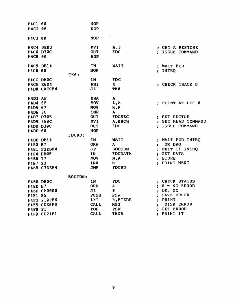
F4C1 00 Nap F4C2 00 Nap
F4C3 00 NOP
F4C4 JEI3 MVI A,3 ; GET A RESTORE E'4C6 038C OUT FDC ISSUE COMMAND f'4C8 01 NOP
F4C9 0814 IN WAIT ; WAIT FOR E'4CB 00 NOP INTRQ
TK0: F4CC OBOC IN FDC F4CE E604 ANI 4 CHECK TRACK " F40B CACCF4 JZ TK0
F403 AF XRA A F404 6F MOV L,A POINT AT LaC 0 F405 67 MOV H,A F406 3C INR A F407 D3BE OUT FOCSEC SET SECTOR F409 3E8C MVI A,B8CH GET READ COMMAND F40B 030C OUT FOC ISSUE COMMAND F4DD 80 NOP
FDCRO: f'4DE D814 IN WAIT WAIT FOR INTRQ F4EfJ 87 ORA A OR ORQ F4E1 F2EBF4 JP BOOTON EXIT IF IN'I'RQ F4E4 DBBF IN FOCOATA GET DATA E4E6 77 MOV M,A STORE F4E7 23 INX H ;. POIN'l' NEXT F4E8 C3DEF4 JMP FOCRD
BOOTDN: F4EB DB0C IN FOC CHECK S'l'ATUS F'4EO B7 ORA A ~ = NO ERROR F4EE CAee00 JZ 0 i OK, GO F4Fl F5 PUSH PSW SAVE ERROR F4F2 210FF6 LXI H,BTERR PRINT F4F5 CDE6F0 CALL MSG DISK ERROR F4F8 F1 POP PSW GE'l' ERROR F4F9 C021Fl CALL THXB PRINT IT
9

INPUT / OUTPUT PORT ASSIGMENTS
Address
00 01 02 03 04 05 06 07 08 09 0A 0B 0C OD 0E 0F 10 11 12 13 14 15 16 17 18 19 lA IB Ie lD It: IF
Read/Write Read/Write Read/Write Read/Write Read/Write Read/W ro i te ~rite
Wr i te Read/Write Read/Write Read/Write Read/Write Read/Write Read/Write Read/Wr i te Read/Write
Read/W'r i te Write write
Function
S10 Channel A Data port SIO Channel A Status/Control Port SIO Channel B Data port SIO ChannelB Status/Control Port PIO Channel A Data port PIO Channel B Data port PIO Channel A Control port PIO Channel B Control Port c'rc Channel 0 Control Port CTC Channel 1 Control Portal CTC Channel 2 Control Port CTC Channel 3 Control Port FDC Command/States Port FDC Track Register FDC Sector Register FDe Data Port Unused Unused Unused Unused FDC .5yncronization/Drive/Density S100 Buss Extended Address A16-A24 On-Board Memory Control Port Unused Unused Unused Unused Unused Unused Unused Unused Unused
All addresses are listed in Hexidecimal.
The unused input / output ports are internally decoded and
should not be used by external 5100 I/O boards.
10
4.0 INPUT / OUTPUT PORT DISCRIPTIONS
4.1 S(;[icl1 Communications Port A --- See Appendux A 00 Read/Wlite SIO Channel A Data port 01 Read/Write SIO Channel A Status/Control Port
4.2 Serial Communications POlt B --- See Append(;x A
4.3
4.4
02 03
Read/Write Reao/writE:.:
paralled Interface POlt A
04 06
Read/Wr i te \~t it€:
parallel Interface Port B
SIO Channel B Data pOlt 510 Channcl B Stc.ltus/Control Pot t
See Appendix B
PIO Channel A Data POlt PIO Channel A Control Pott
See Appenoix B
'lhis port can be jumpered via jumpers E through P to the
5100 vedtoted Interrupt lines or to connector J2 (see sec 6.0 )
05 07
Read/Write Writ.e
PIO Channel B Data port PIO Channel B Control Port
4.5 Control 'rimmer Inlellul-'t circuit --- SeE.! 1-.ppendix C
4 .6
08 09 0A 08
Floppy 0C 0D 0E
" I·
Read/Write Read/Write Read/Write Read/Wlile
Disk ContLollcl Read/Wlite Read/Write Hcad/Write Head/Wr i te
e'1'C Channel 0 Control POL t C'IC Challn~l 1 Control POll C'fC Channe 1 2 Con II 01 Po r l eTC Challnel 3 Control Port
See Appendix D FDe Command/States Port FDC Ttack Register FOe Sector Register FOC Oa ta Po r l
11
4.7 Floppy Disk Contlol Port 14 Read/Write FDC Syncronization/Drive/Density
Port Read : CC
When the cpu reads this port the cpu is placed into e wail
state until a data byte can be transfered to or from the flopp)
disk controller or untill the command complete/terminate status
(INTRO) is set by the floppy disk controller. The floppy disk
controller INTRQ status bit is placed on the data bus as bit D7.
This bit can be tested to determine if data is to be transfered
of if the command is complete.
+----+----+----+----+----+----+----+----+ ! D7 ! D6 ! D5 1 04 ! 03 ! 02 ! DilDO ! +----+----+----+----+----+----+----+----+
1 1 1 II! I 1 +--I! I 1 +-------I I I I +------------1 ! +-----------------+---------------------I +---------------------------1 +--------------------------------+-------------------------------------
Port write:
D7 = MSB, D0 = LSB
Don't care Don't care Don't care Don't care Don't care Don't cale Don't care INTRQ* 0=active, l=inactive
The low two bits 00 and Dl of this port control which drive is
selected.
Dl D0
" " 1 I
o I
" I
Disk drive" selected Disk drive I selected Disk drive 2 selected Disk drive 3 selected
12

Bit 03 sets the density mode. When bit 03 = 0, single density is
selected. When bit 03 = 1, double density is selected.
+----+----+----+----+----+----+----+----+ ! 07 1 D6 1 05 ! 04 ! 03 ! D2 ! D1 ! DO! 07 = MSB, DC = LSB +----+----+----+----+----+----+----+----+ 111 ! 1 1 +-- Disk drive select bit 00 1 1 +------- Disk drive select bit D1
! 1 1 +------------ SIDE SELECT, 0=HEAD 0,l=HEAD 1 !! +----------------- Density, 0=single, 1=double 1 1 +---------------------- Don't care +--------------------------- Don't care +-------------------------------- Don't care +------------------------------------- Don't care
4.8 Extended address port See section B.1 (buss defination) S100 Buss Extended Address A16-A23 15 Write
Port Write:
This port controls the S100 Extended address lines.
+----+----+----+----+----+----+----+----+ 1 07 ! 06 1 D5 1 04 ! D3 I D2 1 DIlDO! 07 = MSB, 00 = LSB +----+----+----+----+----+----+----+----+
! 1 1 1 ! 1 ! +-- A16
1 II!! +------- A17 I! ! +------------ AlB 1 1 +----------------- A19 1 1 "I +---------------------- A20 1 +--------------------------- A21 +-------------------------------- A22 +------------------------------------- A23
13
4.9 On-Board Memor~ Control Port 16 Write On-Board Memory Control Port
Tilis port controls the onboard memory managment circuit,
Prom enable and disable and power on jump Ieset circuits.
Par L wI i te :
The fout low order bits D0,Dl,D2 and D3 switch the on board memolY
ill 16k banks corresponding to address 0'HJ0h-3FF'Fh,4000H-7FFFH,
8000H-BFF'FH and C000-FFFFH on and off. When a particular bank is
switched off, external S109 memory can be accessed in that
banks address range. This feature a110\-/5 external memory to be
added to the system for multi-user operating systems.
Bit D5 ot this port switches the on-board EPROM on and off.
1'he onboard EPROM occupies address F'000H-F'FFFH. The EPROM
is switched on automatically during reset or power on, the
EPROM contains ~IO aud FDe initialization code along with a
simple debugger and floppy disk cold start loader. After
the operating system i!:i loaded thE:: EPROM can be turned off
so that the ram at address F~HHc"H-F~'FF'H can be accessed.
bit 06 leset the power on jump circuit. Bit 06 must be 5et
l,igh after a reset 01 power on situation before ram can
be accessed.
+ - - - - + - - - - +- - - - + - - - - ... - - - - +-- - - ... - - - - -to - - - - + ! 07 ! 06 1 05 ! 04 1 03 ! D2 ! 01 ! DO ! +----+----+----+----+----+----+----+----+
1 +--
+-------1 1 1 -t.-----------
+----------------+---------------------+--------------------------+--------------------------------+-------------------------------------
14
07 = MSB, 00 = LSB
l=bank on, 0=bank off Memory Bank 0000H-3FFFH Memo I y Bank 4iHH?JH-7f F'FH Memory Bank 8000H-BF'F'FH Menoty Bank C000H-FFFFH Don't care PROM ~nab1e=0, Disable=1 Power on jump reset::l Don' t ca r f-;

5.0 Jumper Definitions
Jumper E'unction
A CPU clock late 2mhz/4mhz B t.xt.ernal/Entt:cnal Tx/Rx cloc:k fot SIO channel A C Bxternal/Enternal 1'x/Rx clock fat 510 channel B o Eight inch - five inch Drive selection E Select 5100 interrupt vector line VI0 OR PINT. P Select 5100 interrupt v€ctor VIO/PINT or Parallel
POlt B bit D0 on J2-25. N Select 5100 interrupt vectot VII 01 Parallel
Port B bit 01 on J2-27. M Select 5100 interrupt vector VI2 or Parallel
Port B bit 02 on J2-29. K Select 5100 interru~t vectol VI3 Ot Parallel
Port B bit 03 on J2-3l. J Select S100 interrupt vcctOl V14 or Parallel
POlt B bit D4 on J2-33. Ii Select 5100 intcl.tupt vector VI5 or Parallel
Port B bit 05 on J2-35. G Sel~ct Sl00 interrupt vector VI6 or Parallel
Port B bit D6 on J2-37. F 5~lect S100 intel[Up~ vector VI? or Parallel
Port B bit D7 on J2-39. R Select 2716 or 2732 EPROM. S Define floppy disk connectol [01 ejght ad five incll
drives. '1' EnaLle I Disable Sln0 bus memory wIite signal on
Jl - 68
6.0 Jumper Descri~tion5
6.1 A CPU clock tate 2mhz/4mhz This jumpea: determines the cpu clock tate. The jumper is locat:(;d below Ie U7.
+----t --- .. ----+ ! 1 ! 2 ! 3 ! +---+---+---+
Install Plug between posts 1 & 2 for 4mhz opetolion.
Install Plug between posts 2 &: 3 fot 281hz operation.
6.2 B External/internal Tx/Rx clock fot SIO channel A
Jumper b connects the SIO channel l\ to €ither the internal baud rate
9 en era lor 0 Ito the con nee tor J 4 pin 9 to l use ins y C' ton 0 U S c~ p pI i l: uti a H S .-
15

Jumper B is located near J5.
+---+ 1 I 1 Connector J5 pin 9 +---+ ! 2 I SIO Tx/Rx clock input +---+ ! 3 ! Baud rate generator channel A +---+
Install Plug between posts 1 & 2 for external SIO clock.
Install Plug between posts 2 & 3 for Baud rate gen.cr8tor.
6.3 C External/internal Tx/Rx clock for SIO channel B
Jumper C connects the SIO channel B to either the internal baud rate
generator or to connector J5 pin 9 for use in sycronous applications.
Jumper C is located near J5.
+---+ ! 1 ! Connector J5 pin 9 +---+ ! 2 ! SIO Tx/Rx clock input +---+ 1 3 ! Baud rate generator channel B +---+
Install Plug between posts I & 2 for external SIO clock.
Install Plug between posts 2 & 3 for Baud rate generator.
6.4 D Eight inch - five inch Drive selection
Jumper D is located near IC U2.
+---+ 1 6 ! 8 inch floppy clock source +---+ ! 5 ! FDC clock input +---+ 1 4 ! 5.25 inch floppy clock source +---+ ! 3 ! 5.25 head load/motor +---+ 1 2 ! Head load source +---+ ! I ! 8 inch head load +---+
Install Plug between posts 1 & 2 and 5 & 6 for 8 drives.
Install Plug between posts 2 & 3 and 4 & 5 for 5.25 inch drives.
16

Note: There ate other board modifications needed to interface
tIle FDe: to a 5.25 inch drive.
6.5 E Select S100 interr~pt vector line VI0 OR PINT.
Jumper E selects the inteltUpt line to be used when channel B
bit 00 is programmed for interrupts.
Jumper E is located below Ie us.
+---+---+---+ ! 1 1 2 ! 3 1 +---+---+---+
Install Plug between posts 1 & 2 for VI0 interrupt pin. (Jl-4)
Install Plug between posts 2 & 3 for PINT interrupt pin. (Jl-73)
6.6 p Select 5100 intertupt vector VIC/PINT Ot Parallel Port B bit 00 on J2-25.
This Jumper is located near connector J2. +---+---+---+ II! 2 ! 3 ! +---+---+---+
Install Plug between posts 1 & 2 to connect the PIO bit 00
to J2 pin 25 (when the PIO bit is programmed for input/output).
Install Plug between posts 2 & 3 to connc~t the PIO bit 00
to the jumper selectoI area E, VI0/PINT (when the PIO bit is
programmed for inter rupt mode).
6.7 N Select 5100 interrupt vector VII or Parallel Port B bit 01 on J2-27.
This jumpet is located near connector J2. +---+---+---+ 1 I 1 2 ! 3 ! +---+---+---+
Install Plug between posts 1 & 2 to connect the PIO bit 01
lo J2 pin 25 (when the PIO bit is ~rogrammed for input/output).
Install Plug between posts 7. & 3 to connect the PIa bit 01
to the vectored interrupt line VII (when the PIO bit is
programmed for intctrupt mode).
17
6.8 M Select 8109 interrupt vector VI2 or Parallel Port B bit 02 on J2-29.
This jumper is located neat connector J2. +---+---+---+ ! 1 ! 2 1 3 ! +---+---+---+
Install Plug between posts 1 & 2 to connect the PIO bit 02
to J2 pin 25 (when the PIO bit is programmed for input/output).
Install Plug between posts 2 & 3 to connect the PIO bit 02
to the vectored interrupt line VI2 (when the PIO bit is
programmed for interrupt mode).
6.9 K Select 8100 interrupt vector VI3 or Parallel Port B bit 03 on J2-31.
This jumper is located near connector J2. +---+---+---+ 1 I ! 2 ! 3 ! +---+---+---+
Install Plug between posts I & 2 to connect the PIO bit D3
to J2 pin 25 (when the PIO bit is programmed for input/output).
Install Plug between posts 2 & 3 to connect the PIO bit 03
to the vectored interrupt line VI3 (when the PIO bit is
programmed for interrupt mode).
6.10 J Select 5100 interrupt vector VI4 01 Parallel Port B bit D4 on J2-33.
This jumper is located near connector J2. +---+---+---+ ! I ! 2 ! 3 ! +---+---+---+
Install Plug between posts I & 2 to connect the PIO bit 04
to J2 pin 25 (when the PIO bit is programmed for input/output).
Install plug between posts 2 & 3 ~o connect the PIO bit D4
to the vectored interrupt linr VI4 (when the PIO bit is
programmed for interrupt mode).
6.11 H Select 5100 interrupt vector VIS or Parallel Port B bit D5 on J2-35.
18

'l'hi s jumper is located near connector J2.
+---+---+---+ ! 1 ! 2 ! 3 ! +--- .... ---+---+
Install Plug between posts 1 & 2 to connect the PlO bit 05
to .12 pill 25 (when the PIa bit is programmed for input/output) •
• Install Plug between posts 2 & 3 to connect the PlO bit 05
to the vectoled interrupt line VIS (when the PlO bit is
programmed for interrupt mode).
6.12 G Select 5100 interrupt vector VI6 or Parallel Port B bit D6 on J2-37.
This jumper is located I.car connectot J2. +---~---+---+
! 1 ! 2 ! 3 ! +---+---+---+
Install Plug between posts 1 & 2 to connect the PIO bit 06
to J2 pin 25 (when the PIO bit is progrpmmed for input/output).
Install plug bet'h'een posts 2 & 3 to connect thE:! PIO bit 06
to the vectored interrupt line VI6 (wherl the PIO bit is
programmed fOl i (Iter rupt mode).
6.13 Select Sl0~ interrupt vector VI7 or Parallel Port B bit 07 on J2-39.
This jumper is located near connector J2. +---i----t----+ ! 1 ! 2 ! 3 ! +---+---+---+
Install Plug between posts 1 & 2 to connect the PIO Lit 07
to J2 ~in 25 (when the PlO bit is programmed for input/output).
Install Plug between posts 2 & 3 to connect the PIO bit 07
to the \tectored interrupt line VI7 (when the PIO bit is
programmed for interru~t mode).
6.14 R Select 2716 or 2732 EPROM.
19
Jumper R configures the board to accept a 2716 or 2732 EPROM.
Jumper R is located near the Z80 chip.
+---+ ! 1 1 Address line All +---+ 1 2 ! EPROM input +---+ ! 3 ! +5 volts +---+
Install plug between posts 1 & 2 fot' a 2732 EPROM.
Install Plug between posts 2 & 3 for a 2716 EPROM.
Note : The EPROM is always addressed at F800H and can not
be moved. Since the 2716 EPROM is 2K long it appears
twice , E800H-FC00H and FBFFH-FFFFH.
6.15 5 Define floppy disk connector for eight , five inch drives and FDC chip type.
This jumper is located U26. +---+---+---+ ! 1 1 2 ! 3 ! +-·--+----r---+ ! 4 ! 5 ! 6 ! +---+---+---+ 171819 ! +---+---+---+ ! ,101 111 121 +---+---+---+
For 8" set-up plug the following jumpers: lto4,2t03,5t06,7to8.
For 5 1/4" plug the following jumpers: Ito2,5to8,6t09,7to10,11to12.(see factory installed jumpers for additional jumpers or changes.)
20
6.16 TEnable / Disable 5100 bus memory write signal on J1 - 68
This jumper is located near U18.
+---+---+ ! 1 ! 2 ! +---+---+
Install Plug between posts 1 & 2 to connect the memory write
signal (MEMWR) to the 5100 bus pin 68.
7.0 Baud Rate Switch
'I'he baud rate of the two serial channels can be select separately
by setting the baud rate switch. The baud rate switch is an 8
pole switch located near U54. It is split into two sections.
switches 1,2,3,4 set the baud rate for the 510 channel
switches 5,6,7,8 set the baud rate for the 510 channel
+-------------------------------+ OFF (up) SW1 ! 8 ! 7 ! 6 ! 5 ! 4 ! 3 ! 2 ! 1 !
+-------------------------------+ ON (down) (- Channel B -) (- Channel A -)
7.1 Baud rate switch setting
Switch Switch
8 4
7 3
6 2
5 1
Channel B baud rate Channel A baud rate
Band
A.
----------------------------------------------------on on on on off on on on on off on on off off on on on on off on off on off on on off off on off off off on on on on off off on on off on off on off off off on off on on off off off on off off on off off off off off off off
For exact baud rate frequencies
50 75 110 134.5 150 300 600 1200 1800 2000 2400 3600 4800 7200 960" 19,200
see Appendix D
21
8.0 External Connector Pin definitions
8.1
PINt
1 2 3 4 5 6 7 8 9 10 11 12 13 ' 14 15 16 17 18 19 20 21 22 23 24 25 26 27,28 29-34 35 36 37 38 39 40-43 44 45 46 47 48 49 50
Connector J1 5100 bus connector
NAME PIN t
+8V 51 +16V 52 XRDY 53 VI0* 54 VIl* 55-57 VI2* 58 VI3* 59 VI4* 60 VI5* 61-64 VI6* 65,65 VI7* 67 NM1* 68 PWRFAIL* 69 DMA3* 70 A18 71 A17 72 A16 73 SOSB* 74 CDSB* 75 GND 76 NDEF 77 ADSS* 78 DOOSB* 79-87 o 88-95 PSTVAL* 96 PHLOA 97 RFU 98 A5,A4,A3,A15,AI2,A9 ~Ol/DATA 1 99 D00/DATA 0 100 A10 004 DOS 006,012,OI3,DI7 SMI SOUT SINP SMEMR SHLTA CLOCK GND
22
NAME
+8V -16V GND SLAVE CLR* DMAO*-DMA2* SXTRQ* A19 SIXTN* A20-A23 NDEF PHAN'l'OM* MWRT RFU GND RFU ROY INT* HOLO* RESET~;
PSYNCH PWR* POBIN A0-A11 D02-010 SINTA SWO* ERROR*
POC* GNO

8.2 Connector J2 Parallel port connector
1 ARDY PIO Channel A ready signal 2 AROY RET ground 3 AS'l'RB* PIO Channel A strobe 4 ASTRB RET ground 5 PA0 PlO Channel A data bit 00 6 PA0 RET ground 7 PAl PIO Channel A data bit 01 8 PAl RET ground 9 PA2 PIO Channel A data bit 02 10 PA2 RET ground 11 FA3 PIO Channel A data bit 03 12 PA3 RET ground 13 PA4 PIO Channel A data bit 04 14 PA4 RET ground 15 PA5 PIO Channel A data bit 05 16 PAS RET ground 17 PA6 PlO Channel A data bit 06 18 PA6 RET ground 19 PA7 PlO Channel A data bit 07 20 PA7 RET ground 21 BROY PIO Channel B ready signal 22 BROY RET ground 23 BSTRB· PIO Channel B strobe 24 BSTRB RET ground
* 25 PB0 PIO Channel B data bit 00 26 PB0 RET ground
* 27 PBI PIO Channel B data bit 01 28 PBI RET ground
* 29 PB2 PlO Channel B data bit D2 30 PB2 RET ground
* 31 PB3 PIO Channel B data bit 03 32 PB3 RET ground
* 33 PB4 PIO Channel B data bit D4 34 PB4 RET ground
... 35 PBS PIO Channel B data bit 05 36 PBS RET ground
* 37 PB6 PIO Channel B data bit D6
38 PB6 RET ground 39 PB7 PIO Channel B data bit D7 40 + 5 VOLTS
-Ie Note : These pins can can be jumpered to the 5100 bus
vectored interrupt lines.
23

8.3 Connector J3 Floppy disk connector
8 inch 5.25 inch
1 ground 2 Alternate Head 2* 3 ground 4 N/C 5 ground 6 N/C ~ ground I
8 N/C 9 ground 10 N/C 11 glound 12 N/C 13 ground 14 Head 2* 15 ground 16 N/C l7 1 ground 18 2 Head load* 19 3 ground 20 4 Index* 21 5 ground 22 6 Ready* 23 7 ground 24 8 Above Track 43* 25 9 ground 26 10 Drive select 0"" 27 11 ground 28 12 Drive select 1* 29 13 ground 30 l4 Drive select 2* 31 15 ground 32 16 Drive select 3'11
33 17 ground 34 18 Direction 35 19 ground 36 20 Step* 37 21 ground 38 22 Write Data* 39 23 ground 40 24 Write gate* 41 25 ground 42 26 Track 0* 43 27 glound 44 28 Write protect* 45 29 ground 46 30 Read data* 47 31 ground 48 32 Motor on* 49 33 ground 50 34 N/C
24

8.4 Connector J4 Serial port Channel A
1 N/C 2 DCDA* Data Carrer Detect Channel A * 3 SYNCA* Sync Detect 4 RxDA Receive data 5 CTSA* Clear to send 6 TxDA Transmit data 7 RTSA* Request to send 8 DTRA* Data terminal ready 9 Tx/RxCA* Transmitt / receive clock 10 GND 11 N/C 12 +16 VOLTS 13 -16 VOLTS 14 +5 VOLTS
8.5 Connector J5 Serial port Channel B
1 N/C 2 DeDA* Data Carrer Detect Channel A ". 3 SYNCA" Sync Detect 4 RxDA Receive data 5 CTSA* Clear to send 6 TxDA Transmit data 7 RTSA* Request to send 8 DTRA* Data terminal ready 9 Tx/RxCA* Transmitt / receive clock 10 GND 11 N/C 12 +16 VOLTS 13 -16 VOLTS 14 +5 VOL'I'S
25

+-----------+ ! connector ! +-+-----+---+
1 ! +-------+ +-----+jumpers!
+-+-----+--+ ! Parallel !
ports +--+-------+
+--+----+
+------------+ ! connector +-----+------+
+-----+------+ ! Floppy disk! ! controller! +-----+------+
+----+ !conn! +-+--+
+----+ !conn! +--+-+
!
+-+---------+-+ ! A Serial B ! 1 ports +-----+-------+
+----+---------------------------+--------------------+
~-----+ !clock!
+-----+
+-------+--+ ! data rec.! ! /drivers ! +-----------1-
+-+
+-----+ +-----+------+ leprom! CPU !2k,4k+--+--+ +-----+ +------------+
+-------+------+ ! 5100 address ! ! drivers +-------+------+
+-----+-------+ Ram Array!
! +-----+-------+
VI lines
+-----------------------------+
+----+---------+-----------+---------------------------------+ S100 BUS
f------------------------------------------------------------+
26

10.0 Factory Installed Jumpers
10.1 Factory Installed jumpers for 8 inch floppy option
Jumper
A B C D E F G H J K M N P R S T
2-3 2-3 2-3 1-2,5-6 1-2 2-3 2-3 2-3 2-3 2-3 2-3 2-3 2-3 2-1 1,2;2,3;5,6;7,8 1-2
CPU clock 4mhz Tx/Rx clock for SIO A internal Tx/Rx clock for SIO B internal Eight inch Drive selection Select vector line VI0 parallel Port B bit 00 on J2-2S. Parallel Port B bit 01 on J2-27. Parallel Port B bit D2 on J2-29. Parallel Port B bit D3 on J2-3l. parallel Port B bit D4 on J2-33. Parallel Port B bit os on J2-3S. parallel Port B bit 06 on J2-37. Parallel Port B bit D7 on J2-39. Select 2716 define floppy disk connector Enable 5100 bus memory write signal
27

10.2 Factory Installed jumpers for 5.25 inch floppy option
Jumper
A 2-3 CPU clock 4mhz B 2-3 Tx/Rx clock for SIO A internal C 2-3 Tx/Rx clock for 510 B internal o 1-2,5-6 Eight inch Drive selection E 1-2 Select vector line VI0 F 2-3 Parallel Port B bit 00 on J2-25. G 2-3 Parallel Port B bit 01 on J2-27. H 2-3 . Parallel Port B bit 02 on J2-29. J 2-3 Parallel Port B bit 03 on J2-31. K 2-3 Parallel Port B bit 04 on J2-33. M 2-3 Parallel Port B bit 05 on J2-35. N 2-3 Parallel Port B bit 06 on J2-37. P 2-3 Parallel Port B bit 07 on J2-39. R 2-1 Select 2716 5 1,2;5,8;6,9;7,10;11,12 Define floppy disk connector T 1-2 Enable 5100 bus memory write signal
(to convert an 8" board to 5-1/4" the following is required in addi-tion to the addendum)
Capacitor C22 is changed to a 100pf or parallel a 47pf with it. capacitor C6 is changed to a 10mf. Resistor R4 is changed to 220k ohm Re-adjust the phase lock loop by adjusting the R26 pot. An easy way to adjust would be to put one trace of the scope on pin 7 of the u27(74s124) and the other channel on a 2 MHZ.
28

10.3 Shugart SA 800 Jumpers
Disk drive jumpers
Remove all jumpers on the disk drive. Install jumpers as follows:
10.4
Jumper y Jumper C Jumper T2 Jumper '1'1 Jumper 800 Jumper L Jumper A Jumper B Jumper OS
Shugart 850 -----------
Disk drive Jumpers
Jumper 25 Jumper C Jumper A Jumper B Jumper R Jumper I Jumper Y Jumper 850 Jumper 52 Jumper IT Jumper FS Jumper RM Jumper HL Jumper S Jumper M Jumper FM,MFM DSl for drive land 052 for drive 2 install termination at the end of cable.
10.6 MFE Model 700
Disk drive jumpers
Install jumpers as follows:
Jumper J3 Jumper J1-4,Jl-8 C Jumper RHL Jumper J10
Jumper J4 Jumper J7 Jumper L-1 Jumper 5S! Jumper J3 Jumper SE2 Jumper WPl Jumper Jll,HS1
29
10.7 TANDON SLIM LINE
Disk drive jumpers
Install jumpers as follows:
DSl OR DS2 INSTALL THE TERMINATION RES. AT THE END OF THE CABLE
10.8 NEC model FDl160
Disk drive Jumpers
Install jumpers as follows:
Jumper C Jumper N Jumper HLS Jumper M
Jumper PRI Jumper DLD Jumper FU
10.9 QUME data track 8
Disk drive jumpers
Install jumpers as follows:
DSI OR DS2 CUT X CUT Z CUT L INSTALL Y INSTALL C
10.9.1 TANDON 5 1/4 " DRIVE(48TPI)
Disk drive jumpers
Install jumpers as follows: On the dip shunt header only pin2,7,8 are on. for DS1 and pins3,7,8 for DS2.
30

11.0 Appendex & Data sheets
11.1 Appendex A - Z80A S10 / DART •••••••••••
31

• Two independent full-duplex channels with separate modem controls. Modem status can be monitored.
• Receiver data registers are quadruply buffered; the transmitter is doubly buffered.
• Interrupt features include a programmable interrupt vector, a "status affects vector" mode for fast interrupt processing, and the standard Z-80 peripheral daisy-chain interrupt structure that provides automatic interrupt vectoring with no external logic.
The Z-80 DART (Dual-Channel Asynchronous Receiver/Transmitter) is a dual-channel multi-function peripheral compOnent that satisfies a wide variety of asynchronous serial data communications requirements in microcomputer systems. The Z-80 DART is used as a serial-to-parallel, parallel-to-serial converterl controller in asy.nchronous applications. In addition, the device also provides modem controls for both channels. In applications where
RaGA
Ilia ToDA
r.a WiIiIm
!ill
}~ IITIl CTIl Imm IR!IJl
RaDB
IiiTil!I ToDB
WiiiiiiI
-}~ DTRB
IR!1II
1-= COIITIIOL iOiiQ
~ : IIIl
+5Y GND CLK
Flgun I. _ DART PIll FUIICtloaII
18470 zaer DUI' .aI Alyac:laroB.as _I .. r' ........... n.r
Prodacl IpacHlc:ad.B
March 1981
• In xl clock mode, data rates are 0 to SOOK bits/second with a 2.5 MHz clock, or 0 to BOOK hits/second with a 4.0 MHz clock.
• Programmable options include I, 1 Y2 or 2 stop bits; even, odd or no parity; and xl, xI6, x32 and x64 clock modes.
• Break generation and detection as well as parity-, overrun- and framing-error detection are available.
modem controls are not needed, these lines can be used for general-purpose VO.
Zilog also offers the Z-80 SIO, a more versatile device that provides synchronous (Bisync, HDLC and SDLC) as well as asynchronous operation.
The Z-80 DART is fabricated with n-channel silicon-gate depletion-load technology, and is packaged in a 40-pin plastic or ceramic DIP.
0, «I Do Us 31 U.
Clf.A Os 31 D.
II-, 37 De IRT 31 iiiiil:i lEi 35 er
lEO 34 1111
III 33 CIO Yoo 32 1m
WiIIliYl 10 31 GND
m II Z·NDAIIT
30 W/RDYB RaDA 12 21 lUI
RiCA 13 • !bOB
~ 14 27 iiiTi9 ToGA 15 21 ToDB
CN·. I5fiIl Ie 25 iiiiiii IifiA ~ 17 24 ii'fii CfiA ~ II 23 CTii ~ " 22 6eI5I
CLK ... 20 21 mn
89
I i

PIn DMcrIptioD
90
B/A. Channel A Or B Select (input, High selects Channel B). This input defines which channel is accessed during a data transfer between the CPU and the Z-80 DART.
C/D. Control Or Data Select (input, High selects Control). This input specifies the type of information (control or data) transferred on the data bus betwe,en the CPU and the Z-80 DART.
CE. Chip Enable (input, activ~ Low). A Low at this input enables the Z-80 DART to accept command or data input from the CPU during a write cycle, or to transmit data to the CPU during a read cycle.
CLK. System Clock (input). The Z-80 DART uses the standard Z-80 single-phase system clock to synchronize internal signals.
CTSA. CTSB. Clear To Send (inputs, active Low). When programmed as Auto Enables, a Low on these inputs enables the respective transmitter. If not programmed as Auto Enables, these inputs may be programmed as general-purpose inputs. Both inputs are Schmitt-trigger buffered to accommodate slowrisetime signals.
Do-D,. System Data Bus (bidirectional, 3-state) transfers data and commands between the CPU and the 2-80 DART.
DCDA. DCDB. Data Carrier Detect (inputs, active Low). These pins function as receiver enables if the Z-80 DART is programmed for Auto Enables;· otherwise they may be used as general-purpose input pins. Both pins are Schmitt-trigger buffered.
DTRA. DTRB. Data Terminal Ready (outputs, active Low). These outputs follow the state programmed into the DTR bit. They can also be programmed as general-purpose outputs.
lEi. Interrupt Enable In (input, active High) is used with lEO to form a priority daisy chain when there is more than one interrupt-driven device. A High on this line indicates that no other device of higher priority is being serviced by a CPU interrupt service routine.
lEO. Interrupt Enable Out (output, active High). lEO is High only if lEI is High and the CPU is not servicing an interrupt from this Z-80 DART. Thus, this signal blocks lower priority devices from interrupting while a higher priority device is being serviced by its CPU interrupt service routine.
INT. Interrupt Request (output, open drain, active Low). When the Z-80 DART is requesting an interrupt, it pulls INT Low.
NI. Machine Cycle One (input from Z-80 CPU, active Low). When MI and RD are both active, the 2-80 CPU is fetching an instruction from memory; when Ml is active while 10RQ is active, the Z-80 DART accepts MI and IORQ
as an interrupt acknowledge if the Z-80 DART is the highest priority device that has iriterrupted the 2-80 CPU.
IORQ. Input/Output Request (input from CPU, active Low). 10RQ is used in conjunction with B/A, c/o, CE and RD to transfer commands and data between the CPU and the 2-80 . DART. When CE, RD and 10RQ are all active, the channel selected by BIA transfers data to the CPU (a read operation). When CE and 10RQ are active, but RD is inactive, the channel selected by B/A is written to by the CPU with either data or control information as specified by c/o. RxCA. RxCB. Receiver Clocks (inputs). Receive data is sampled on the rising edge of RxC. The Receive Clocks may be 1, 16,32 or 64 times the data rate.
RD. Read Cycle Status. (input from CPU, active Low). If RD is active, a memory or 110 read operation is in progress.
RxDA. RxDB. Receive Data (inputs, active High).
RESET. Reset (input, active Low). Disables both receivers and transmitters, forces TxDA and TxDB marking, forces the modem controls High and disables all interrupts.
RIA. RIB. Ring Indicator (inputs, Active Low). These inputs are similar to CTS and DCD. The Z-80 DART detects both logic level transitions and interrupts the CPU. When not used in switched-line applications, these inputs can be used as general-purpose inputs.
RTSA. RTSB. Request to Send (outputs, active Low). When the RTS bit is set, the RTS output goes Low. When the RTS bit is reset, the output goes High after the transmitter empties.
TxCA. TxCB. Transmitter Clocks (inputs). TxD changes on the falling edge of TxC. The Transmitter Clocks may be I, 16, 32 or 64 times the data rate; however, the clock multiplier for the transmitter and the receiver must be the same. The Transmit Clock inputs are Schmitt-trigger buffered. Both the Receiver and Transmitter Clocks may be driven by the 2-80 CTC Counter Time Circuit for programmable baud rate generation.
TxDA. TxDB. Transmit Data (outputs, active High).
W/ltDYA. W/RDYB. Wait/Ready (outputs, open drain when programmed for Wait function, driven High and Low when programmed for Ready function). These dual-purpose outputs may be programmed as Ready lines for a DMA controller or as Wait lines that synchronize the CPU to the Z-80 DART data rate. The reset state is open drain.

FUDCtloaai o.cnptloa
2044·001
The functional capabilities of the Z-80 DART can be described from two different points of view: as a data communications device, it transmits and receives serial data, and meets the requirements of asynchronous data communications protocols; as a Z-80 family peripheral, it interacts with the Z-80 CPU and other Z-80 peripheral circuits, and shares the data, address and control buses, as well as being a part of the Z-80 interrupt structure. As a peripheral to other microprocessors, the Z-BO DART offers valuable features such as nonvectored interrupts, polling and simple hand-
CommuDlcatloDB CapablUties. The Z-80 DART provides two independent full-duplex channels for use as an asynchronous receiver/transmitter. The following is a short description of receiver/transmitter capabilities. For more details, refer to the Asynchronous Mode section of the Z-80 S10 Technical Manual. The Z-80 DART offers transmission and reception of five to eight bits per character, plus optional even or odd parity. The transmitter can supply one, one and a half or two stop bits per character and can provide a break output at any time. The receiver break detection logic interrupts the CPU both at the start and end of a received break. Reception is protected from spikes by a transient spike rejection mechanism that checks the signal onehalf a bit time after a Low level is detected on the Receive Data input. If the Low does not persist-as in the case of a transient-the character assembly process is not started.
1/0 lat.rface Capabllltles. The Z-80 DART offers the choice of Polling, Interrupt (vectored or non-vectored) and Block Transfer modes to transfer data, status and control information to
OATA ....
CPU SUS tID
CONTROl. ••• L __ J
INTERRUPT CONTROl.
LINES
f f f +IVGND CLK
INTERNAl CONTROl.
LOGIC
INTERRUPT CONTROl
LOGIC
shake capability. The first part of the follOWing functional
description introduces Z-80 DART data communications capabilities; the second part describes the interaction between the CPU and the Z-80 DART.
A more detailed explanation of Z-80 DART operation can be found in the Z-80 S10 Technical Manual (Document Number 03-3033-00. Because this manual was written for the Z-80 SIO, it contains information about synchronous as well as asynchronous operation.
Framing errors and overrun errors are detected and buffered together with the character on which they occurred. Vectored interrupts allow fast servicing of interrupting conditions using dedicated routines. Furthermore, a built-in checking process avoids interpreting a framing error as a new start bit: a framing error results in the addition of one-half a bit time to the point at which the search for the next start bit is begun.
The Z-80 DART does not require symmetric Transmit and Receive Clock signals-a feature that allows it to be used with a Z-80 CTC or any other clock source. The transmitter and receiver can handle data at a rate of 1, 1116, 1/32 or 1164 of the clock rate supplied to the Receive and Transmit Clock inputs. When using Channel B, the bit rates for transmit and receive operations must be the same because RxC and TxC are bonded together (RxTxCB).
and from the CPU. The Block Transfer mode can be implemented under CPU or DMA control.
CHANNEL A RIEADlWRITE REGISTERS
CHANNELS RIEADlWRtTE I:EGlSTEAS
SERIAl DATA
CHANNEL CLOCKS
WiITiII6lW
_OR OTHER CONTROLS
MODEM OR OTHER CONTROlS
Ail
SERiAl DATA
CHANNEL ClOCK WAiliiimiV
Figure 3. Block Diagram
91
I I

Fu~c:tloDal DetlcrlptloD (Continued)
92
POLLING. There are no interrupts in the Polled mode. Status registers RRO and.RRl are updated at appropriate times for each function being performed. All the interrupt modes of the Z-80 DART must be disabled to operate the device in a polled environment.
While in its Polling sequence, the CPU examines the status contained in RRO for each channel; the RRO status bits serve as an acknowledge to the Poll inquiry. The two RRO
INTERRUPTS. The Z-80 DART offers an elaborate interrupt scheme that prOVides fast interrupt response in real-time applications. As a member of the Z-80 family, the Z-80 DART can be daisy-chained along with other Z-80 peripherals for peripheral interrupt-priority resolution. In addition, the internal interrupts of the Z-80 DART are nested to prioritize the various interrupts generated by Channels A and B. Channel B registers WR2 and RR2 contain the interrupt vector that points to an interrupt service routine in the memory. To eliminate the necessity of writing a status analysis routine, the Z-80 DART can modify the interrupt vector in RR2 so it points directly to one of eight interrupt service routines. This is done under program control by setting a program bit (WRl, O2) ip Channel B called "Status Affects Vector." When this bit is set, the interrupt vector in RR2 is modified according to the assigned priority of the various interrupting conditions.
Transmit interrupts, Receive interrupts and External/Status interrupts are the main sources of interrupts. Each interrupt source is enabled under program control with Channel A having a higher priority than Channel B, and with Receiver. Transmit and External/Status interrupts prioritized in that order within each channel. When the Transmit interrupt is enabled, the CPU is interrupted by the transmit buffer becoming empty. (This implies that the transmitter must have had a data character written into it so it can become
CPUIDMA BLOCK TRANSFER. The Z-80 DART provides a Block Transfer mode to accommodate CPU block transfer functions and DMA block transfers (Z-80 DMA or other designs). The Block Transfer mode uses the W /RDY output in conjunction with the Wait/Ready bits of Write Register 1. The W/RDY output can be defined under software control as aWait line in the CPU Block
. status bits Do and O2 indicate that a data transfer is needed. The status also indicates Error or other special status conditions (see "Z-80 DART Programming"). The Special Receive Condition status contained in RRI does not have to be read in a Polling sequence because the status bits in RRlare accompanied by a Receive Character Available status in RRO.
empty.) When enabled, the receiver can interrupt the CPU in one of three ways:
• Interrupt ,on the first received character
• Interrupt on all received characters
• Interrupt on a Special Receive condition
Interrupt On First Character is typically used with the Block Transfer mode. Interrupt On All Receive Characters can optionally modify the interrupt vector in the event of a parity error. The Special Receive Condition interrupt can occur on a character basis. The Special Receive condition can cause an interrupt only if the Interrupt On First Receive Character or Interrupt On All Receive Characters mode is selected. In Interrupt On First Receive Character, an interrupt can occur from Special Receive conditions (except Parity Error) after the first receive character interrupt (example: Receive Overrun interrupt).
The main function of the External/Status interrupt is to monitor the signal transitions of the CTS, OeD and RI pins; however, an External/Status interrupt is also caused by the detection of a Break sequence in the data stream. The interrupt caused by the Break sequence has a special feature that allows the Z-80 DART to interrupt when the Break sequence is detected or terminated. This feature facilitates the proper termination of the curren! message, correct initialization of the next message, and the accurate timing of the Break condition.
Transfer mode or as a Ready line in the DMA Block Transfer mode.
To a DMA controller, the Z-80 DART Ready output indicates that the Z-80 DART is ready to transfer data to or from memory. To the CPU, the Wait output indicates that the Z-80 DART is not ready to transfer data, thereby requesting the CPU to extend the 110 cycle.
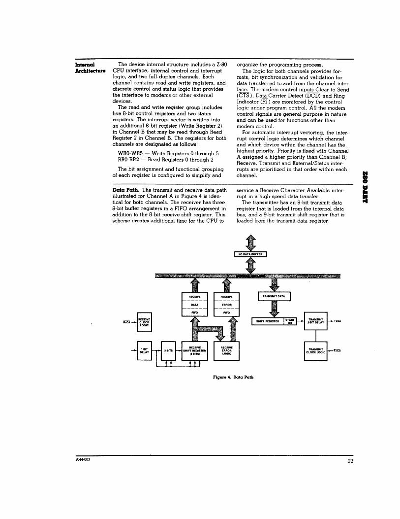
Internal ArchItecture
2044-003
The device internal structure includes a 2-80 CPU interface, internal control and interrupt logic, and two full-duplex channels. Each channel contains read and write registers, and discrete control and status logic that provides the interface to modems or other external devices.
The read and write register group includes five 8-bit control registers and two status registers. The interrupt vector is written into an additional 8-bit register (Write Register 2) in Channel B that may be read through Read Register 2 in Channel B. The registers for both channels are designated as follows:
WRO-WRS - Write Registers 0 through S RRO-RR2 - Read Registers 0 through 2
The bit assignment and functional grouping of each register is configured to simplify and
Data Path. The transmit and receive data path illustrated for Channel A in Figure 4 is identical for both channels. The receiver has three 8-bit buffer registers in a FIFO arrangement in addition to the 8-bit receive shift register. This scheme creates additional time for the CPU to
organize the programming process. The logic for both channels provides for
mats, bit synchronization and validation for data transferred to and from the channel interface. The modem control inputs Clear to Send (CTS), Data Carrier Detect (DCD) and Ring Indicator (HI) are monitored by the control logic under program control. All the modem control signals are general purpose in nature and can be used for functions other than modem control.
For automatic interrupt vectoring, the interrupt control logic determines which channel and which device within the channel has the highest priority. Priority is fixed with Channel A assigned a higher priority than Channel B; Receive, Transmit and External/Status interrupts are prioritized in that order within each channel.
service a Receive Character Available interrupt in a high-speed data transfer.
The transmitter has an 8-bit transmit data register that is loaded from the internal data bus, and a 9-bit transmit shift register that is loaded from the transmit data register.
Figure 4. Data Path
93
I i

Read. Write aDCl Interrupt TlmlDg
94
Read Cycle. The timing signals generated by a Z-80 CPU input instruction to read a Data or
Writ. Cycle. Figure Sb illustrates the timing and data signals generated by a Z-80 CPU out-
Interrupt Aclmowledge Cycle. After receiving an Interrupt Request signal (INT pulled Low), the Z-OO CPU sends an Interrupt Acknowledge signal (MI and IORQ both Low). The daisy-chained interru'pt circuits determine the highest priority interrupt requestor. The lEI of the highest priority peripheral is terminated High. For any peripheral that has no interrupt pending or under service, lEO = lEI. Any peripheral that does have an interrupt pending or under service forces its lEO Low.
Return From Interrupt Cycle. Normally, the Z-80 CPU issues an RETI (Return From Interrupt) instruction at the end of an interrupt service routine. RETI is a 2-byte opcode (ED-4D) that resets the interrupt-under-service latch to terminate the interrupt that has just been processed.
CLOCK
CE ------,~+-------------'
~----------~--------------------DATA ----------------0000(0...---
Figure Sa. Read Cycle
CLOCK
~ ~'--------, ' ___ I
iiD--------------------------------~r_--__.~-----IEI _________ I \ ____ _
DATA----------------~~~------
Figure Sc. Interrupt Acknowledge Cycle
Status byte from the Z-80 DART are illustrated in Figure Sa.
put instruCtion to write a Data or Control byte into the Z-80 DART.
To insure stable conditions in the daisy chain, all interrupt status signals are prevented from changing while MI is Low. When IORQ is Low, the highest priority interrupt requestor (the one with lEI High) places its interrupt vector on the data bus and sets its internal interrupt-under-service latch.
Refer to the Z-80 SIO Technical Manual for additional details on the interrupt daisy chain and interrupt nesting.
When used with other CPUs, the Z-80 DART allows the user to return from the interrupt cycle with a special command called "Return From Interrupt" in Write Register 0 of Channel A. This command is interpreted by the Z-80 DART in exactly the same way it would interpret an RET! command on the data bus.
CLOCK
Ci ----Rti---------------------------~------------------------------
DATA __________ -J)(~ _____ IN _____ >e::::: Figure 5b. Write Cycle
IEI------ I ------.1 lEO r---_______ ...IJ
'
Figure 5d. Return from Interrupt Cycle
2044-008, 009, OW, 011

Z-80 DART Programming
To program the Z-80 DART, the system program first issues a series of commands th(lt initialize the basic mode and then other commands that qualify conditions within the selected mode. For example, the character length, clock rate, number of stop bits, even or odd parity are first set, then the Interrupt mode and, finally, receiver or transmitter enable.
Write Registers. The Z-80 DART contains six registers (WRO-WR5) in each channel that are programmed separately by the system program to configure the functional personality of the channels (Figure 4). With the exception of WRO, programming the write registers requires two bytes. The first byte contains three bits (Do-D2) that point to the selected register; the second byte is the actual control word that is written into the register to configure the Z-80 DART.
WRO is a special case in that all the basic commands- (CMDo-CMD2) can be accessed with a single byte. Reset {internal or external} initializes the pointer bits Do-D2 to point to WRO. This means that a register cannot be
Read Registers. The Z-80 DART contains three registers (RRO-RR2) that can be read to obtain the status information for each channel (except for RR2, which applies to Channel B only). The status information includes error conditions, interrupt vector and standard communications-interface signals.
To read the contents of a selected read register other than RRO, the system program must first write the pointer byte to WRO in exactly the same way as a write register operation. Then, by executing an input instruction, the contents of the addressed read register can be read by the CPU.
Both channels contain command registers that must be programmed via the system program prior to operation. The Channel Select input (BfA) and the ControVData input (CfD) are the command structure addressing controls, and are normally controlled by the CPU address bus.
pointed to in the same operation as a channel reset.
Write Register Functions
WRO Register pointers, initialization commands for the various modes, etc.
WRI TransmitlReceive interrupt and data transfer mode definition.
WR2 Interrupt vector (Channel B only)
WR3 Receive parameters and control
WR4 TransmitlReceive miscellaneous parameters and mooes
WR5 Transmit parameters and controls
The status bits of RRO and RRI are carefully grouped to simplify status monitoring. For example, when the interrupt vector indicates that a Special Receive Condition interrupt has occurred, all the appropriate error bits can be read from a single register (RRl).
Read Register FundioDS
RRO TransmitlReceive buffer status, interrupt status and external status
RRI Special Receive Condition status
RR2 Modified interrupt vector (Channel B only)
95
I §

READ REGISTER 0
I~~I~ ~ ~I~I~I~I
Z-80 DART Read and Write Reglsten
~~I L: :TC;E:~:.~~:~:~:~~ ~ T. BUFFER EMPTY
~D } USED WITH "EXTERNAU CTS STATUS INTERRUPT" NOT USED MODE
96
READ REGISTER I"
L-NOTUSED
PARITY ERROR
~--------------BRPK
ID~7ID~'!Ds~ID~'~~ALLSENT R. OVERRUN ERROR
FRAMING ERROR
NOT USED "Used Wllh Special Receive Condition Mode
WRITE REGISTER 0
1~1~IDsiDsIDsIDsI~IDsI
T-C! o 0 NULL CODE o 0 NOT USED
REGISTER 0 REGISTER 1 REGISTER 2 REGISTER 3 REGISTER 4 REGISTER 5
o 1 RESET EXT/STATUS INTERRUPTS o 1 CHANNEL RESET 1 0 ENABLE INT ON NEXT R. CHARACTER 1 0 RESET hiNT PENDING 1 1 ERROR RESET 1 1 RETURN FROM INT (CH·A ONLy)
L------------NOT USED
WRITE REGISTER 2 (CHANNEl. B ONLY)
1~IDsIDsIDsIDslDsI~IDsI
~I ~~ !INTERRUPT ~V4 VECTOR
VS
V6
L----------------V7
WRITE REGISTER 4
1~IDs!Ds!DsiDsIDsI~IDsI
ITT I L PARITY ENABLE
L PARITY EVEN/ODfi
o 0 NOT USED o 1 1 STOP BIT/CHARACTER 1 0 1 'I. STOP BITS/CHARACTER 1 1 2 STOP BITS/CHARACTER
NOT USED
o 0 Xl CLOCK MODE o 1 Xl6 CLOCK MODE 1 0 X32 CLOCK MODE 1 1 X64 CLOCK MODE
READ REGISTER 2
1~IDsIDsIDsI~I~I~IDsI
~I ~~:: !INTERRUPT ~V4 VECTOR
VS
VI
~------------- V7 ""Variable JI ·Slatus Affects
Vector Is Programmed
WRITE REGISTER 1
T ~L EXT INT ENABLE
L T. INT ENABLE STATUS AFFECTS VECTOR (CH. BONlY)
o 1 R. INT ON FIRST CHARACTER OR ON o 0 R. INT DISABLE }
1 0 IN!;>F~~~~ :~gT'6AR~ACTER. S (PARITY :~~~:~~ INT ON All Rx CHARACTERS (PARITY CONDITION
DOES NOT AFFECT VECTOR) L--______ WAIT/READY ON R/T
L-. ______ WAIT/READY FUNCTION
'------- WAIT/READY ENABLE
WRITE REGISTER 3
1~IDsIDsIDsIDsIDsI~I~1
L-- NOT USED
"--------- AUTO ENABLES T I ~ LR.ENABlE
Rx 5 BITS/CHARACTER R. 7 BITS/CHARACTER Rx I BITS/CHARACTER R. 8 BITS/CHARACTER
WRITE REGISTER 5
1~IDsIDsIDsiDs!~!~IDsI
T ~I ~ :~;USED ~ NOTUSED
T. ENABLE
SEND BREAK
o 0 Tx 5 BITS (OR lESS)lCHARACTER o 1 T. 7 BITS/CHARACTER 1 0 Tx 6 BITS/CHARACTER 1 1 T.8 BITS/CHARACTER
"-----DTR
2044·()()4.oo5

11.2 Appendex B - Z80A PIO ••••••••••••••••••
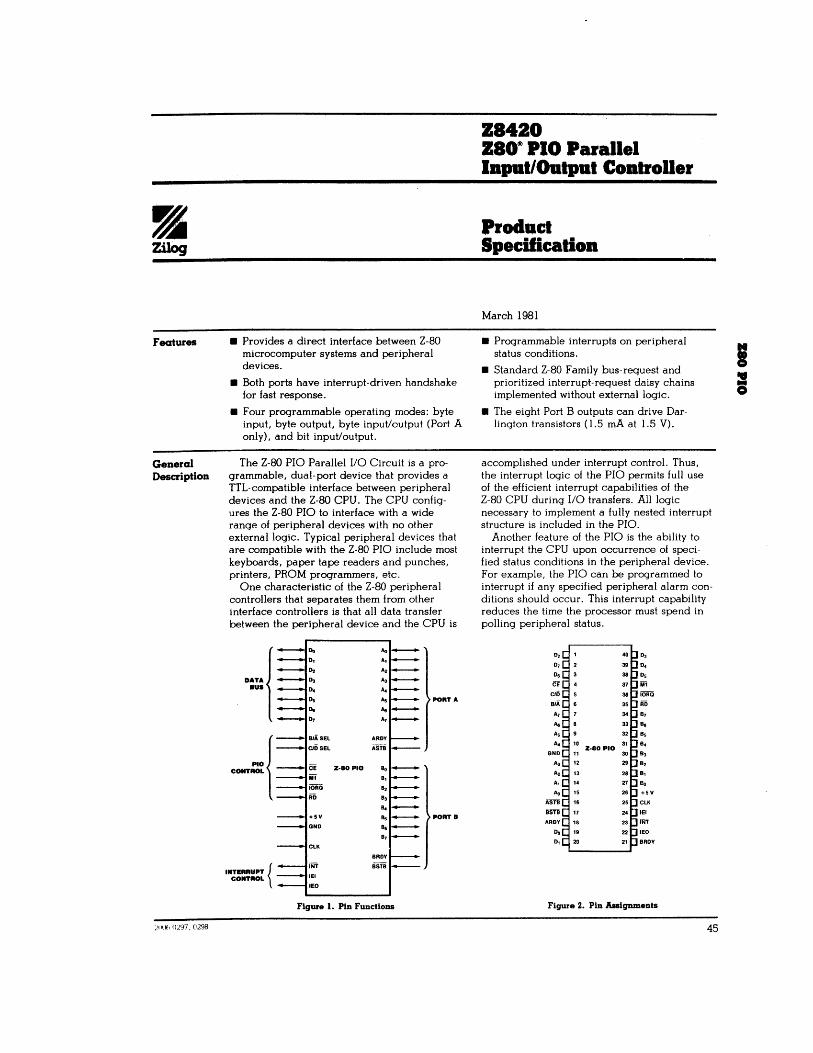
Features
General Description
}IHII, 0297,0298
• Provides a direct interface between Z-80 microcomputer systems and peripheral devices.
• Both ports have interrupt-driven handshake for fast response.
• Four programmable operating modes: byte input, byte output, byte input/output (Port A only), and bit input/output.
The Z-80 PIO Parallel I/O Circuit is a programmable, dual-port device that provides a TTL-compatible interface between peripheral devices and the Z-80 CPU. The CPU configures the Z-80 PIO to interface with a wide range of peripheral devices with no other external logic. Typical peripheral devices that are compatible with the Z-80 PIO include most keyboards, paper tape readers and punches, printers, PROM programmers, etc.
One characteristic of the Z-80 peripheral controllers that separates them from other interface controllers is that all data transfer between the peripheral device and the CPU is
UTA/ aus
"oj CONTROL
INTURUPT { CONTROL
PORTA
ASTB
Z-80PIO
8,
PORTB
lEO
Figure 1. Pin Functions
Z8420 Z80~ PIO Parallel lapat/Oatpat Coatroller
Prodac:t Spec:Uic:atioa
March 1981
• Programmable interrupts on peripheral status conditions.
• Standard Z-80 Family bus-request and prioritized interrupt-request daisy chains implemented without external logic.
• The eight Port B outputs can drive Darlington transistors (1.5 rnA at 1.5 V).
accomplished under interrupt control. Thus, the interrupt logic of the PIO permits full use of the efficient interrupt capabilities of the Z-80 CPU during 110 transfers. All logiC necessary to implement a fully nested interrupt structure is included in the PIa.
Another feature of the PIa is the ability to interrupt the CPU upon occurrence of specified status conditions in the peripheral device. For example, the PIO can be programmed to interrupt if any speCified peripheral alarm conditions should occur. This interrupt capability reduces the time the processor must spend in polling peripheral status.
D,~ 1 40 0,
D,~ 39 D.
D6E 38 OS
CE 37 M1 c/o 38 lORa
B/A 35 iiii A, 34 B,
Aa 33 B6
As 32 Bs
Aa 10 Z·80 PIO
31 B.
GND 11 30 B,
A, 12 29 B,
A, 13 28 IJ B,
A, 14 27 Bo
Aa 15 26 +5V
ASTB 16 25 ClK
BSTB 17 24 lEI
ARDY 18 23 iNT Do 19 22 lEO
D, 20 21 BRDY
Figure 2. Pin Assignments
45
I ! o

General Description (Continued)
46
The Z-80 PIO interfaces to peripherals via two independent general-purpose I/O ports, designated Port A and Port B. Each port has eight data bits and two handshake signals, Ready and Strobe, which control data transfer. The Ready output indicates to the peripheral that the port is ready for a data transfer. Strobe Is an input from the peripheral that indicates when a data transfer has occurred.
Operating Modes. The Z-80 PIO ports can be programmed to operate in' four modes: byte output (Mode O), byte input (Mode 1), byte input/output (Mode 2) and bit input/output (Mode 3).
In Mode 0, either Port A or Port B can be programmed to output data. Both ports have output registers that are individually addressed by the CPU; data can be written to either port at any time. When data is written to a port, an active Ready output indicates to the external device that data is available at the associated port and is ready for transfer to the external device. After the data transfer, the external device responds with an active Strobe input, which generates an interrupt, if enabled.
In Mode I, either Port A or Port B can be configured in the input mode. Each port has an input register addressed by the CPU. When the CPU reads data from a port, the PIO sets the Ready signal, which is detected by the external device. The external device then places data on the I/O lines and strobes the I/O port, which latches the data into the Port Input Register, resets Ready, and triggers the Interrupt Request, if enabled. The CPU can read the input data at any time, which again sets Ready.
Mode 2 is bidirectional and uses Port A, plus the interrupts and handshake signals from both PGfts. Port B must be set to Mode 3 and masked off. In operation, Port A is used for both data input and output. Output operation is similar to Mode 0 except that data is allowed out onto the Port A bus only when ASTB is Low. For input, operation is similar to Mode 1, except that the data input uses the Port B handshake signals and the Port B interrupt (if enabled).
Both ports can be used in Mode 3. In this mode, the individual bits are defined as either input or output bits. This proVides up to eight separate, individually defined bits for each port. During operation, Ready and Strobe are
not used. Instead, an interrupt is generated if the condition of one input changes, or if all inputs change. The requirements for generating an interrupt are defined during the programming operation; the active level is specified as either High or Low, and the logic condition is specified as either one input active (OR) or all inputs active (AND). For example, if the port is programmed for active Low inputs and the logic function is AND, then all inputs at the speCified port must go Low to' generate an interrupt.
Data outputs are controlled by the CPU and can be written or changed at any time.
• Individual bits can be masked off.
• The handshake signals are not used in Mode 3; Ready is held Low, and Strobe is disabled.
• When using the Z-80 PIO interrupts, the Z-80 CPU interrupt mode must be set to Mode 2.
RxCA
TxCA
RxCD
fiCa
SYSTEM BUSES
PIG
lEI
lEO
INT
lEI
RDY
DMA
Figure 3. PIO in a Typical zaD Family Environment
2041-0156
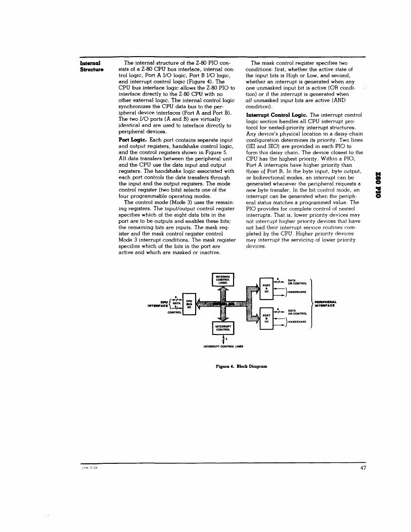
Internal Structure
"I'llf, !llIh
The internal structure of the Z-80 PIa consists of a Z-80 CPU bus interface, internal controllogic, Port A I/O logic, Port B I/O logic, and interrupt control logic (Figure 4). The CPU bus interface logic allows the Z-80 PIO to interface directly to the Z-80 CPU with no other external logic. The internal control logic synchronizes the CPU data bus to the peripheral device interfaces (Port A and Port B). The two I/O ports (A and B) are virtually identical and are used to interface directly to peripheral devices.
Port Logic. Each port contains separate input and output registers, handshake control logic, and the control registers shown in Figure 5. All data transfers between the peripheral unit and the CPU use the data input and output registers. The handshake logic associated with each port controls the data transfers through the input and the output registers. The mode control register (two bits) selects one of the four programmable operating modes.
The control mode (Mode 3) uses the remaining registers. The input/output control register specifies which of the eight data bits in the port are to be outputs and enables these bits; the remaining bits are inputs. The mask register and the mask control register control Mode 3 interrupt conditions. The mask register specifies which of the bits in the port are active and which are masked or inactive.
INTERRUPT CONTROL LINES
The mask control register specifies two conditions: first, whether the active state of the input bits is High or Low, and second, whether an interrupt is generated when any one unmasked input bit is active (OR condition) or if the interrupt is generated when all unmasked input bits are active (AND condition) .
Interrupt Control Logic. The interrupt control logic section handles all CPU interrupt protocol for nested-priority interrupt structures. Any device's physical location in a daisy-chain configuration determines its priority. Two lines (lEI and lEO) are prOVided in each PIa to form this daisy chain. The device closest to the CPU has the highest priority. Within a PIa, Port A interrupts have higher priority than those of Port B. In the byte input, byte output, or bidirectional modes, an interrupt can be generated whenever the peripheral requests a new byte transfer. In the bit control mode, an interrupt can be generated when the peripheral status matches a programmed value. The PIa provides for complete control of nested interrupts. That is, lower priority devices may not interrupt higher priority devices that have not had their interrupt service routines completed by the CPU. Higher priority devices may interrupt the servicing of lower priority devices.
DATA OR CONTROL
} HANDSHAKE
DATA OR CONTROL
} HANDSHAKE
PERIPHERAL IIIT.PACE
Figure 4. Block Diagram
47
I B
Internal Structure (Continued)
48
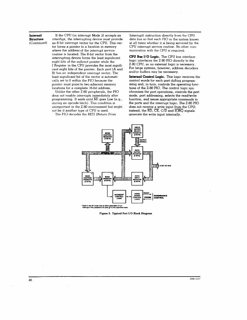
If the CPU (in interrupt Mode 2) accepts an interrupt. the interrupting device must provide an 8-bit interrupt vector for the CPU. This vector forms a pointer to a location in memory where the address of the interrupt service routine is located. The 8-bit vector from the interrupting device forms the least significant eight bits of the indirect pointer while the I Register in the CPU provides the most significant eight bits of the pointer. Each port (A and B) has an independent interrupt vector. The least significant bit of the vector is automatically set to 0 within the PIO because the pointer must point to two adjacent memory locations for a complete 16-bit address.
Unlike the other 2-80 peripherals, the PIO does not enable interrupts immediately after programming. It waits until M1 goes Low (e.g., during an opcode fetch). This condition is unimportant in the 2-80 environment but might not be if another type of CPU is used.
The PIO decodes the RETI (Return From
MODE CONTROL REGISTER
(2 BITS)
INTERRUPT CONTROL
lOGIC
'U_ In the bll mode only 10 a._llllnaralion 01 an Inl,,"upl II the peripheral UO plnl go 10 the lpaclfled Ilate.
Interrupt) instruction directly from the CPU data bus so that each PIO in the system knows at all times whether it is being serviced by the CPU interrupt service routine. No other communication with the CPU is required.
CPU Bus 1/0 Logic. The CPU bus interface logic interfaces the 2-80 PIO directly to the 2-80 CPU, so no external logic is necessary. For large systems, however, address decoders and/or buffers may be necessary.
Intemal Control Logic. This logic receives the control words for each port duf-ing programming and, in turn, controls the operating functions of the 2-80 PIO. The control logic synchronizes the port operations, controls the port mode, port addressing, selects the read/write function, and issues appropriate commands to the ports and the interrupt logic. The 2-80 PIO does not receive a write input from the CPU; instead, the RD, CE, cii5 and IORQ signals generate the write input internally.
HANDSHAKE
CONTROL lOGIC
II-BIT UO BUS
READY } HANDSHAKa
STROBE CONTROL
Figure S. Typical Port 1/0 Block Diagram
20060317

ProgrClllUDing Mode O. 1. or 2. (Byte Input, Output, or Bidirectional). Programming a port for Mode 0, 1, or 2 requires two words per port. These words are:
A Mode Control Word. Selects the port operating mode (Figure 6). This word may be written any time.
An Interrupt Vector. The Z-80 PIO Is designed for use with the Z-80 CPU in interrupt Mode 2 (Figure 7). When interrupts are enabled, the PIO must provide an interrupt vector.
Mode 3. (Bit Input/Output). Programming a port for Mode 3 operation requires a control word, a vector (if interrupts are enabled), and three additional words, described as follows:
1/0 Register Control. When Mode 3 is selected, the mode control word must be followed by another control word that sets the I/O control register, which in turn defines which port lines are inputs and which are outputs (Figure 8).
IDr\o.IDSID.I' I, I ' I ' I
I T L,_.~_, CONTROL WORD
DON'T CARE
MODE SELECT
MODED MODE' MODE 2 MODE 3
Figure 6. Mode Control Word
IDrI~\~I~I~I~I~lol
I L IDENTIFIES INTERRUPT
VECTOR
L ____ ~~~~O~PPLIED INTERRUPT
Figure 7. Interrupt Vector Word
IDrIDeI~I~I~I~I~IDeI I D SETS BIT TO OUTPUT
, SETS BIT TO INPUT
Figure 8. 1/0 Register Control Word
20060318.0319.0320,0321.0322,0323
Interrupt Control Word. In Mode 3, handshake is not used. Interrupts are generated as a logic function of the input signal levels. The interrupt control word sets the logic conditions and the logic levels required for generating an interrupt. Two logic conditions or functions are available: ANO (if all input bits change to the active level, an interrupt is triggered), and OR (if anyone of the input bits changes 10 the active level, an interrupt is triggered). Bit 0 6 sets the logic function, as shown in Figure 9. The active level of the input bits can be set either High or Low. The active level is controlled by Bit 05.
Mask Control Word. This word sets the mask control register, allowing any unused bits to be masked off. If any bits are to be masked, then 0 4 must be set. When 04 is set, the next word written to the port must be a mask control word (Figure 10).
Interrupt Disable. There is one other control word which can be used to enable or disable a port interrupt. It can be used without changing the rest of the interrupt control word (Figure II).
III L ::::::::, ro~ D. = , MASK WORD FOLLOWS
Ds = 0 ACTIVE LEVEL IS LOW Ds = 1 ACTIVE LEVEL IS HIGH
D8 = 0 INTERRUPT ON OR FUNCTION ~ = , INTERRUPT ON AND FUNCTION
L-_______ ~ : ~ :~~~::~:~ ~~::t:~.
·NOTE: THE PORT IS NOT ENABLED UNTIL THE INTERRUPT ENABLE IS FOLLOWED BY AN ACTIVE iii.
Figure 9. Interrupt Control Word
IDrlo.l~I~I~I~I~IDeI
I MBo-MB7 MASK BITS. A BIT IS MONITORED FOR AN
L. ---- INTERRUPT IF IT IS DEFINED AS AN INPUT AND THE MASK BIT IS SET TO D.
Figure 10. Mask Control Word
IDrIDeI~ID.1 0 I D I, 1'1 1 T c= IDENTIFIES INTERRUPT DISABLE WORD
DON'TCARE
Dr = 0 INTERRUPT DISABLE 07 = , INTERRUPT ENABLE
Figure II. Interrupt Disable Word
49

Pin DeKrlptloD
50
Ao-A,. Port A Bus (bidirectional, 3-state). This a-bit bus transfers data, status, or control information between Port A of the PIO and a peripheral device. Ao is the least significant bit of the Port A data bus.
ARDY. Register A Ready (output, active High). The meaning of this signal depends on the mode of operation selected for Port A as follows:
Output Mode. This signal goes active to indicate that the Port A output register has been loaded and the peripheral data bus is stable and ready for transfer to the peripheral device.
Input Mode. This signal is active when the Port A input register is empty and ready to accept data from the peripheral device.
Bidirectional Mode. This signal is active when data is available in the Port A output register for transfer to the peripheral device. In this mode, data is not placed on the Port A data bus, unless ASTB is active.
Control Mode. This signal is disabled and forced to a Low state.
ASTB. Port A Strobe Pulse From Peripheral Device (input, active Low). The meaning of this signal depends on the mode of operation selected for Port A as follows:
Output Mode. The positive edge of this strobe is issued by the peripheral to acknowledge the receipt of data made available by the PIO.
Input Mode. The strobe is issued by the peripheral to load data from the peripheral into the Port A input register. Data is loaded into the PIO when this signal is active.
Bidirectional Mode. When this signal is active, data from the Port A output register is gated onto the Port A bidirectional data bus. The positive edge of the strobe acknowledges the receipt of the data.
Control Mode. The strobe is inhibited internally.
80-1,. Port B Bus (bidirectional, 3-state). This 8-bit bus transfers data, status, or control information between Port B and a peripheral device. The Port B data bus can supply 1.5 rnA at 1.5 V to drive Darlington transistors. Eo is the least Significant bit of the bus.
B/X. Port B Or A Select (input, High = B). This pin defines which port is accessed during a data transfer between the CPU and the PIa. A Low on this pin seleds Port A; a High selects Port B. Often address bit Ao from the CPU is used for this selection function.
BRDY. Register B Ready (output, active High). This signal is similar to ARDY, except that in the Port A bidirectional mode this signal is High when the Port A input register is empty and ready to accept data from the peripheral device.
BSTB. Port B Strobe Pulse From Peripheral Device (input, active Low). This signal is similar to ASTB, except that in· the Port A bidirectional mode this signal strobes data from the peripheral device into the Port A input register.
,
C/O. Control Or Data Select (input, High = C). This pin defines the type of data transfer to be performed between the CPU and the PIa. A High on this pin during a CPU write to the PIa causes the Z-80 data bus to be interpreted as a command for the port selected by the BiA Select line. A Low on this pin means that the Z-80 data bus is being used to transfer data between the CPU and the PIa. Often address bit A I from the CPU is used for this function.
CEo Chip Enable (input, active Low). A Low on this pin enables the PIO to accept command or data inputs from the CPU during a write cycle or to transmit data to the CPU during a read cycle. This signai is generally decoded from four I/O port numbers for Ports A and B, data, and control. CLK. System Clock (input). The Z-80 PIO uses the standard single-phase Z-80 system clock.
00-0,. Z8G CPU Data Bus (bidirectional, 3-state). This bus is used to transfer all data and command~ between the 2-80 CPU and the Z-80 PIa. Do is the least significant bit.
lEI. Interrupt Enable In (input, active High). This signal is used to form a priority-interrupt daisy chain when more than one interruptdriven device is being used. A High level on this pin indicates that no other devices of higher priority are being serviced by a CPU interrupt service routine.
lEO. Interrupt Enable Out (output, active High). The lEO signal is the other signal required to form a daisy chain priority scheme. It is High only if lEI is High and the CPU is not servicing an interrupt from this PIa. Thus this signal blocks lower priority devices from interrupting while a higher priority device is being serviced by its CPU interrupt service routine.
INT. Interrupt Request (output, open drain, active Low). When INT is active the 2-80 PIa is requesting an interrupt from the 2-80 CPU.
IORQ. Input/Output Request (input from 2-80 CPU, active Low). IORQ is used in conjunction with B/A, C/O, CE, and RD to transfer commands and data between the 2-80 CPU and the 2-80 PIa. When CE, RD, and IORQ are active, the port addressed by B/A transfers data to the CPU (a read operation). Conversely, when CE and IORQ are active but RD is not, the port addressed by BiA Is written into from the CPU with either data or control information, as speCified by C/O. Also, if 10RQ and MI are active simultaneously, the CPU is acknowledging an interrupt; the interrupting port automatically places its interrupt vector on the CPU data bus if it is the highest priority device requesting an interrupt.

Pin Desc:rlptlon ( Continued)
TlmlDg
MI. Machine Cycle (input from CPU, active Low). This signal is used as a sync pulse to control several internal PIa operations. When both the MI and RD signals are active, the 2-80 CPU is fetching an instruction from memory. Conversely, when both Ml and 10RQ are active, the CPU is acknowledging an interrupt. In addition, MI has two other functions within the 2-80 PIa: it synchronizes
The folloWing timing diagrams show typical timing in a 2-80 CPU environment. For more precise specifications refer to the composite ac timing diagram.
Write Cycle. Figure 12 illustrates the timing for programming the 2-80 PIa or for writing data to one of its ports. No Wait states are allowed for writing to the PIa other than the automatically inserted TWA. The PIa does not receive a specific write signal; it internally generates its own from the lack of an active RD signal.
Read Cycle. Figure 13 illustrates the timing for reading the data input from an external device to one of the 2-80 PIa ports. No Wait states are allowed for reading the PIO other than the automatically inserted TWA.
Output Mode (Mode 0). An output cycle (Figure 14) is always started by the execution of an output instruction by the CPU. The WR· pulse from the CPU latches the data from the CPU data bus into the selected port's output register. The WR· pulse sets the Ready flag after a Low-going edge of CLK, indicating data is available. Ready stays active until the positive edge of the, trobe line is received, indicating that data WdS taken by the peripheral. The positive edge of the strobe pulse generates an INT if the interrupt enable flipflop has been set and if this device has the highest priority.
CLK
PORT
the PIa interrupt logic; when Ml occurs without an active RD or 10RQ Signal. the PIa is. reset.
RD. Read Cycle Status (input from 2-80 CPU, active Low). If "Ro is active, or an 110 operation is in progress, RD is used with B/A, C/O, CE, and 10RQ to transfer data from the 2-80 PIa to the 2-80 CPU.
T, T2 TWA T3 T,
eLK
e/i),.,i =:::x >e:= Ci
IORO \ r-DATA X IN x= WR' \ r-
'WR = RD • CE • C/D • IORO
Figure 12. Write Cycle Timing
T, T, TWA T3 T,
eLK
C/O,./i ==x >C Ci " I
IORO \ I AD \ I
DATA ( OUT >-RD' \ I
ORO = RD • CE • C/O • IORO
Figure 13. Read Cycle Timing
OUTPUT ------J'----+-----f----I--
READY
° WR = RO. CE • C/O • IORO
Figure 14. Mode 0 Output Timing
2006,0324. 0325, 0326
N
I • ... 0
51

Timing (Continued)
52
Input Moel. (Mod. 1). When STROBE goes Low, data is loaded into the selected port input register (Figure 15). The next rising edge of strobe activates INT, if Interrupt Enable is set and this is the highest-priority requesting device. The following falling edge of CLK resets Ready to an inactive state, indicating
*RD = RD. CE • C/O. IORQ
that the input register is full and cannot accept any more data until the CPU completes a read. When a read is complete, the positive edge of RD sets Ready at the next Low-going transition of CLK. At this time new data can be loaded into the PIO.
Figure 15. Mod. 1 Input Timing
Bidirectional Moel. (Mode 2). This is a combination of Modes 0 and I using all four handshake lines and the eight Port A 110 lines (Figure 16). Port B must be set to the bit mode and its inputs must be masked. The Port A handshake lines are used for output control and the Port B lines are used for input control.
eLK
ARDY
If interrupts occur, Port A's vector will be used during port output and Port B's will be used during port input. Data is allowed out onto the Port A bus only when ASTB is Low. The rising edge of this strobe can be used to latch the data into the peripheral.
~RTA _____________________ ~~~~=>--------~ DATA BUS
BRDY
*WR = RD· CE • CtD • IORQ
Figure 16. Mode 2 Bidirectional Timing
2006-0327. 0328

TlmlDg (Continued)
)(KIh lH29 tn<o (n 11
Bit Mode (Mode 3). The bit mode does not utilize the handshake signals, and a normal port write or port read can be executed at any time. When writing, the data is latched into the output registers with the same timing as the output mode (Figure 17).
When reading the PIO, the data returned to the CPU is composed of output register data from those port data lines assigned as outputs and input register data from those port data
eLK
lines assigned as inputs. The input register contains data that was present immediately prior to the falling edge of RD. An interrupt is generated if interrupts from the port are enabled and the data on the port data lines satisfy the logical equation defined by the 8-bit mask and 2-bit mask control registers. However, if Port A is programmed in bidirectional mode, Port B does not issue an interrupt in bit mode and must therefore be polled.
DATA~:; ____ --'X DATA WOAD 1 X DATA WOAD 2
t
"Timing Diagram Refers to Bit Mode Read =0 1 PLACED ON 8US ~ Figure 17. Mode 3 Bit Mode Timing
Interrupt Acknowledge Timing. During Ml time, peripheral controllers are inhibited from changing their interrupt enable status, permitting the Interrupt Enable signal to ripple through the daisy chain. The peripheral with lEI High and lEO Low during INTACK places a preprogrammed S-bit interrupt vector on the data bus at this time (Figure IS). lEO is held Low until a Return From Interrupt (RETI) instruction is executed by the CPU while lEI is High. The 2-byte RETI instruction is decoded internally by the PIO for this purpose.
Return From Interrupt Cycle. If a Z-80 peripheral has no interrupt pending and is not under service, then its lEO = lEI. If it has an interrupt under service (Le., it has already interrupted and received an interrupt acknowledge) then its lEO is always Low, inhibiting lower priority devices from interrupting. If it has an interrupt pending which has not yet been acknowledged, lEO is Low unless an "ED" is decoded as the first byte of a 2-byte opcode (Figure 19). In this case, lEO goes High until the next opcode byte is decoded, whereupon it goes Low again. If the second byte of the opcode was a "4D," then the opcode was an RET I instruction.
After an "ED" opcode is decoded, only the peripheral device which has interrupted and is currently under service has its lEI High and its
•••
Figure 18. Intenupt Acknowledge Timing
lEO Low. This device is the highest-priority device in the daisy chain that has received an interrupt acknowledge. All other peripherals have lEI = lEO. If the next opcode byte decoded is "4D," this peripheral device resets its "interrupt under service" condition.
__________________ ~r____ Figure 19. Retwn From Intenupt
I B
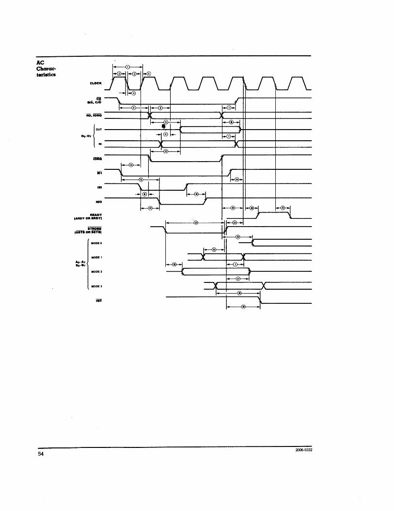
AC Characteristics
54
CLOCK
Ci 8Ii,eli)
RD,IORQ -------------r-1~----_1----------------~~~~~~---------+-------------
Do-D7 {OUT
IN
lEi
lEO
READY IARDY OR aROY,
iiiiiiii (iiii OR UTa.
IIODEO
MODE 1
IIODE2
IIODE3
2006-0332

Z-8O PlO Z-8OA PlO Z-80B Pl0I9) lila Max MID Max MID Max
N~ Symbol Parameter (as)- (as) (as) (as) (-) (as) Comment
TcC Clock Cycle Time 400 [I) 250 [1) 165 [I)
2 TwCh Clock Width (High) 170 2000 105 2000 65 2000
3 TwCI Clock Width (Low) 170 2000 105 2000 65 2000
4 TfC Clock Fall Time 30 30 20
5-TrC Clock Rise Time 30 30 20
6 TsCS(RI) CE, BiA, cm to RD, IORO I Setup Time 50 50 50 [6)
7 Th Any Hold Times for Specified Setup Time 0 0 0 0
8 TsRI(C) RD, IORO to Clock f Setup Time 115 115 70
9- TdRI(OO)-- RD, IORO Ito Data Out Delay 430 380 300 [2)--
10 TdRI(DOs) RD, IORO t to Data Out Float Delay 160 110 70 N
11 TsDI(C) Data In to Clock t Setup Time 50 50 40 CL = 50 pF • TdIO(DOI) IORQ I to Data Out Delay
0 12 • (INTACK Cycle) 340 160 120 [3) .. 13- TsMl(Cr)-- MI I to Clock t Setup Time-- 210 90 70 0
14 TsMl(Cf) MI--Lto Clock I Setup Time (MI Cycle) 0 0 0 [8)
IS TdMI(IEO) MI I to lEO I Delay (Interrupt Immediately Preceding MI I) 300 190 100 [5,7)
16 TsIEI(IO) lEI to IORO I Setup Time (INTACK Cycle) 140 140 100 [7)
17 - T dIEI(IEOf)- lEI I to lEO I Delay 190 130 120 [5)--CL = 50 pF
18 TdIEI(IEOr) lEI t to lEO t Delay (after ED Decode) 210 160 160 [5)
19 TcIO(C) IORQ t to Clock I Setup Time (To Activate READY on Next Clock Cycle) 220 290 170
20-TdC(RDYr)- Clock I to READY t Delay---200 190 170 [5)--CL = 50 pF
21 TdC(RDYf) Clock I to READY t Delay 150 140 120 [5)
22 TwSTB ""STROBE Pulse Width 150 150 120 [4)
23 TsSTB(C) ~ t to Clock I Setup Time (To Activate READY on Next Clock Cycle) 220 220 150 [5)
24 -TdIO(PD)-- IORQ t to PORT DATA Stable Delay (Mode 0) 200 180 160 (5)
25 TsPD(STB) PORT DATA to ~ t Setup Time (Mode I) 260 230 190
26 TdSTB(PD) STROBE I to PORT DATA Stable (Mode 2) 230 210 180 [5)
27 -TdSTB(PDr)-STROBE I to PORT DATA Float Delay (Mode 2) 200 180 160 CL = 50 pF
28 TdPD(INT) PORT DATA Match to INT I Delay (Mode 3) 540 490 430
29 TdSTB(lNT) ~ I to 1Nf I Delay 490 440 350
NOTES: [61 TsCS(Rl) may be reduced. However. the time subtracted III TcC = TwCh + TwCI + TrC + TIC. from TsCS(Rl) will be added to TdRI(OO). ILl Increase TdRI(DO) by 10 ns for each 50 pF increase in load [71 2.5 TcC > (N-2)TdIEI(IEOf) + TdMI(IEO) + TsIEl(IO)
up to 200 pF max. + TTL Buller Delay. if any. III Increase TdIO(DOI) by 10 ns lor each 50 pF. increase in [81 Ml must be active for a minimum of two clock cycles to
luading up to 200 pF max. reset the PI~. 141 For Mode 2: TwSTB > TsPD(STB). [91 ZSOB PIa numbers are preliminary and subject to change. lSI Increase these values by 2 ns for each 10 pF increase in
loading up to 100 pF max.
55
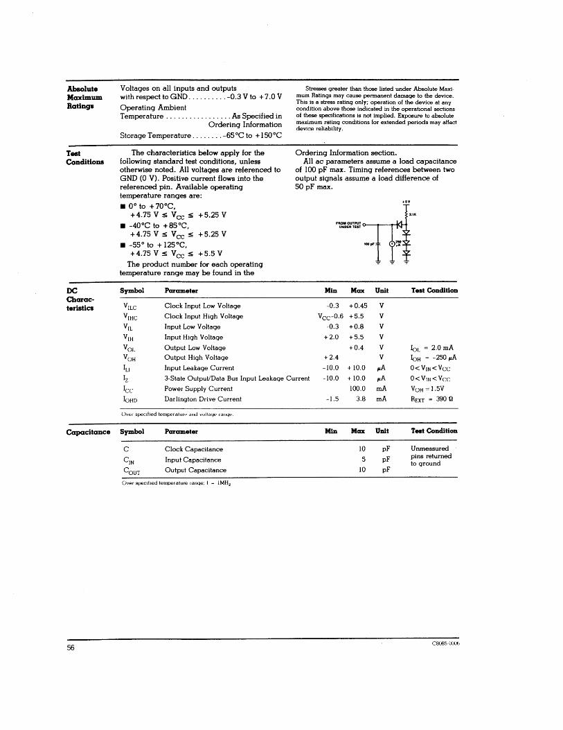
Absolute Maximum Ratings
Test Conditions
DC Charac-teristics
Capacitance
56
Voltages on all inputs and outputs with respect to GND .......... -0.3 V to + 7.0 V Operating Ambient Temperature ................. As Specified in
Ordering Information Storage Temperature ........ -65°C to + 150 °C
The characteristics below apply for the follOWing standard test conditions, unless otherwise noted. All voltages are referenced to GND (0 V). Positive current flows into the referenced pin. Available operating temperature ranges are:
• 0° to + 70°C, +4.75 V $ Vee $ +5.25 V
• -40°C to +85°C, +4.75 V $ Vee $ +5.25 V
• -55° to + 125°C, +4.75 V $ Vee $ +5.5 V
The product number for each operating temperature range may be found in the
Symbol Parameter
VILC Clock Input Low Voltage
V1HC Clock Input High Voltage
VIL Input Low Voltage
VIH Input High Voltage
VOL Output Low Voltage VOH Output High Voltage
ILl Input Leakage Current
Stresses greater than those listed under Absolute Maximum Ratings may cause permanent damage to the device. This is a stress rating only; operation of the device at any condition above those indicated in the operational sections of these specifications is not implied. Exposure to absolute maximum rating conditions for extended periods may affect device reliability.
Ordering Information section. All ac parameters assume a load capacitance
of 100 pF max. Timing references between two output signals assume a load difference of 50 pF max.
.IV
2.1K
Min Max Unit Test Condition
-0.3 +0.45 V
Vcc-0.6 +5.5 V
-0.3 +0.8 V
+2.0 +5.5 V
+0.4 V +2.4 V
-10.0 + 10.0 ~ Iz 3-State Output/Data Bus Input Leakage Current -10.0 + 10.0 p.A
IoL = 2.0 rnA IoH = -250 p.A
O<VIN<VCC
O<VIN<VCC
VOH = 1.5V
REXT = 390 {} Icc Power Supply Current 100.0 rnA
IOHD Darlington Drive Current -1.5 3.8 rnA
Over specified temperaturp dnd voltage range.
Symbol Parameter Min Max Unit Test Condition
C Clock Capacitance 10 pF Unmeasured
C1N Input Capacitance 5 pF pins returned to ground
COUT Output Capacitance 10 pF
Over specliJed temperature range; t = IMHz
C8085UUUb
11.3 Appendex C - Z8~A CTC ••••••••••••••••••

Features
General Description
20410154,0155
• Four independently programmable counter/timer channels, each with a readable down counter and a selectable 16 or 256 prescaler. Downcounters are reloaded automatically at zero count.
• Three channels have Zero Count/Timeout outputs capable of driving Darlington transistors.
The Z-80 eTC four-channel counter/timer can be programmed by system software for a broad range of counting and timing applications. The four independently programmable channels of the Z-80 eTC satisfy common microcomputer !;ystem requirements for event counting, interrupt and interval timing, and general clock rate generation.
System design is Simplified because the eTC connects directly to both the Z-80 CPU and the Z-80 SIO with no additional logic. In larger systems, address decoders and buffers may be required.
Programming the CTe is straightforward:
CPU! DATA BUS
CTC { COIlTROL PROM
CPU
DAISY { CHAIII
IIiTURUPT COIITROL
lEO
iiiT
f f f CLK +5 V GNO
Figure 1. Pin Functions
CHAIlIlau. SIGNALS
18430 zaer eTC Coa.terl ""er Clreult
Prodact SpecUlcatloD
March 1981
• Selectable positive or negative trigger initiates timer operation.
• Standard Z-80 Family daisy-chain interrupt structure provides fully vectored. prioritized interrupts without external logic. The CTC may also be used as an interrupt controller.
• Interfaces directly to the Z-80 CPU or-for baud rate generation-to the Z-80 SIO.
each channel is programmed with two bytes; a third is necessary when interrupts are enabled. Once started, the eTC counts down, reloads its time constant automatically, and resumes counting. Software timing loops are completely eliminated. Interrupt processing is Simplified because only one vector need be speCified; the eTC internally generates a unique vector for each channel.
The Z-80 CTC requires a single + 5 V power supply and the standard Z-80 single-phase system clock. It is fabricated with n-channel silicon-gate depletion-load technology, and packaged in a 28-pin plastic or ceramic DIP.
O. 28 1>3 Os 27 0,
De 28 0,
0, 25 Do GND 24 +5V
RD 23 ClKITAGo
ZClTOo Z~~OA C::C 22 ClKITAG,
ZClTO, 21 ClKITAG,
ZClTo" 20 ClKITAG.
IORO 10 19 CS,
lEO 11 18 CSo
iiiT 12 17 REffi lEI 13 18 CE ii1 14 15 ClK
Figure 2. Pin Assignments
59
I a
FUDCt10Dal Description
Architecture
60
The Z-80 CTC has four independent counterl timer channels. Each channel is individually programmed with two words: a control word and a time-constant word. The control word selects the operating mode (counter or timer), enables or disables the channel interrupt, and selects certain other operating parameters. If the timing mode is selected, the control word also sets a prescaler, which divides the system clock by either 16 or 256. The time-constant word is a value from 1 to 256.
During operation, the individual courtter channel counts down from the preset time constant value. In counter mode operation the counter decrements on each of the CLKlTRG input pulses until zero count is reached. Each decrement is synchronized by the system clock. For counts greater than 256, more than one counter can be cascaded. At zero count, the down-counter is automatically reset with the time constant value.
The timer mode determines time intervals as small as 4 p.s (Z-80A) or 6.4 p.s (Z-80) without additional logic or software timing loops. Time intervals are generated by dividing the system clock with a prescaler that decrements
The CTC has four major elements, as shown in Figure 3.
• CPU bus I/O • Channel control logic • Interrupt logic • Counterltimer circuits CPU Bus 110. The CPU bus I/O circuit decodes the address inputs, and interfaces the CPU data and control signals to the CTC for distribution on the internal bus.
PROM Z80CPU
{
DATA
CONTROL
a preset down-counter. Thus, the time interval is an integral mul
tiple of the clock period, the prescaler value (16 or 256) and the time constant that is preset in the down-counter. A timer is triggered automatically when its time constant value is programmed, or by an external CLKlTRG input.
Three channels have two outputs that occUr at zero count. The first output is a zerocount/timeout pulse at the ZC/TO output. The fourth channel (Channel 3) does not have a ZC/TO output; interrupt request is the only output available from Channel 3.
The second output is Interrupt Request (INT), which occurs if the channel has its interrupt enabled during programming. When the Z-80 CPU acknowledges Interrupt Request, the Z-80 CTC places an interrupt vector on the data bus.
The four channels of the Z-80 CTC are fully prioritized and fit into four contiguous slots in a standard Z-80 daisy-chain interrupt structure. Channel 0 is the highest priority and Channel 3 the lowest. Interrupts can be individually enabled (or disabled) for each of the four channels.
Intemal Control Logic. The CTC internal control logic controls overall chip operating functions such as the chip enable, reset, and read/write logic.
Interrupt Logic. The interrupt control logic ensures that the CTC interrupts interface properly with the Z-80 CPU interrupt system. The logic controls the interrupt priority of the CTC as a function of the lEI signal. If lEI is High, the CTC has priority. During interrupt
iNT lEI
lEO
lCITO
CLKlTRQ
Figure 3. Functional Block Diagram
2041·0157

ArehlteCture (Continued)
/()41 IJI'i"
processing, the interrupt logic holds lEO Low, which inhibits the interrupt operation on lower priority devices. If the lEI input goes Low~ priority is relinquished and the interrupt logic drives lEO Low.
If a channel is programmed to request an interrupt, the interrupt logic drives lEO Low at the zero count, and generates an INT signal to the Z-BO CPU. When the Z-BO CPU responds with interrupt acknowledge (Ml and IORQ), then the interrupt logic arbitrates the CTC internal priorities, and the interrupt control logic places a unique interrupt vector on the data bus.
H an interrupt is pending, the interrupt logic holds lEO Low. When the Z-BO CPU issues a Return From Interrupt (RETn instruction, each peripheral device decodes the first byte (EDI6). If the device has a pending interrupt, it raises lEO (High) for one Ml cycle. This ensures that all lower priority devices can decode the entire RETI instruction and reset properly.
ZClTO
Figure 4. Counter/Timer Block Diagram
Counter/Timer Circuits. The eTe has four independent counter/timer circuits, each containing the logic shown in Figure 4.
Channel Control Logic. The channel control logic receives the 8-bit channel control word when the counter/timer channel is programmed. The channel control logic decodes
the control word and sets the following operating conditions:
• Interrupt enable (or disable) • Operating mode (timer or counter) • Timer mode prescaler factor (16 or 256) • Active slope for CLKITRG input • Timer mode trigger (automatic or CLKlTRG
input) • Time constant data word to follow • Software reset Time CoDStant Register. When the counter/ timer channel is programmed, the time constant register receives and stores an 8-bit time constant value, which can be anywhere from 1 to 256 (0 = 256). This constant is automatically loaded into the down-counter when the counter/timer channel is initialized, and subsequently after each zero count.
Prescaler. The prescaler, which is used only in timer mode, divides the system clock frequency by a factor of either 16 or 256. The prescaler output clocks the down-counter during timer operation. The effect of the prescaler on the down-counter is a multiplication of the system clock period by 16 or 256. The prescaler factor is programmed by bit 5 of the channel control word.
Down-Counter. Prior to each count cycle, the down-counter is loaded with the time constant register contents. The counter is then decremented one of two ways, depending on operating mode:
• By the prescaler output (timer mode) • By the trigger pulses into the CLKITRG
input (counter mode)
Without disturbing the down-count, the Z-80 CPU can read the count remaining at any time by performing an I/O read operation at the port address assigned to the CTC channel. When the down-counter reaches the zero count, the Ze/TO output generates a positivegoing pulse. When the interrupt is enabled, zero count also triggers an interrupt request signal (lNT) from the interrupt logiC.
61
I a

Programming
62
Each Z-80 eTC channel must be programmed prior to operation. Programming consists of writing two words to the 110 port that corresponds to the desired channel. The first word is a control word that selects the operating mode and other parameters; the second word is a time constant, which is a binary data word with a value from 1 to 256. A time constant word must be preceded by a channel control word.
After initialization, channels may be reprogrammed at any time. If updated control and time constant words are written to a channel during the count operation, the count continues to zero before the new tilne constant is loaded into the counter.
If the interrupt on any Z-80 CTC channel is enabled, the programming procedure should also include an interrupt vector. Only one vector is required for all four channels, because the interrupt logic automatically modifies the vector for the channel requesting service.
A control word is identified by a 1 in bit O. A 0 in bit 2 indicates a time constant word is to follow. Interrupt vectors are always addressed to Channel 0, and identified by a 0 in bit O.
Addressing. During programming, channels are addressed with the channel select pins CSI and CS2. A 2-bit binary code selects the appropriate channel as shown in the following table.
Channel CSI CSo
000 1 0 1 2 1 0 3 1 1
Reset. The CTC has both hardware and software resets. The hardware reset terminates all down-counts and disables all CTC interrupts by resetting the interrupt bits in the control registers. In addition, the ZC/TO and Interrupt outputs go inactive, lEO reflects lEI, and
IIITERRUPT J J 1 ENABLES INTERRUPT o DISABLES INTERRUPT .
MODE o SELECTS TIMER MODE
1 SELECTS COUNTER MODE
PRESCALER VALUE" 1 = VALUE OF 256 o = VALUE OF 16
CLKITRO EOOE SELECTIOII o SELECTS FALLING EDGE
1 SELECTS RISING EDGE
00-07 go to the high-impedance state. All channels must be completely reprogramJIled after a hardware reset.
The software reset is controlled by bit I in the channel control word. When a channel receives a software reset, it stops counting. When a software reset is used, the other bits in the control word also change the contents of the channel control register. After a software reset a new time constant word must be written to the same channel.
If the channel control word has both bits Dl and 02 set to 1, the addressed channel stops operating, pending a new time constant word. The channel is ready to resume after the new constant is programmed. In timer mode, if 0 3 = 0, operation is triggered automatically when the time constant word is loaded.
Channel Control Word Programming. The channel control word is shown in Figure 5. It sets the modes and parameters described below.
Interrupt Enable. D7 enables the interrupt, so that an interrupt output (INT) is generated at zero count. Interrupts may be programmed in either mode and may be enabled or disabled at any time.
Operating Mode. 06 selects either timer or counter mode.
Prescaler Factor. (Timer Mode Only). D5 selects factor-either 16 or 256.
Trigger Slope. 0 4 selects the active edge or slope of the CLK/TRG input pulses. Note that reprogramming the CLK/TRG slope during operation is equivalent to issuing an active edge. If the trigger slope is changed by a control word update while a channel is pending operation in timer mode, the result is the same as a CLK/TR G pulse and the timer starts. Similarly, if the channel is in counter mode, the counter decrements.
~L COIITROL OR VECTOR
0= VECTOR 1 = CONTROL WORD
RESET o = CONTINUED OPERATION 1 = SOFTWARE RESET
TIME COIISTAIIT o = NO TIME CONSTANT FOLLOWS 1 = TIME CONSTANT FOLLOWS
TIMER TRIGGER" o = AUTOMATIC HUGGER WHEN
TIME CONSTANT IS LOADED 1 = CLKlTRG PULSE STARTS TIMER
'TIMER MODE ONLY
Figure 5. Channel Control Word
2041-0159

Programming (Continued)
.IU41 UHiO, Ul61
Trigger Mode (Timer Mode Only). D3 selects the trigger mode for timer operation. When D3 is reset to 0, the timer is triggered automatically. The time constant word is programmed during an I/O write operation, which takes one machine cycle. At the end of the write operation there is a setup delay of one clock period. The timer starts automatically (decrements) on the rising edge of the second clock pulse (T 2) of the machine cycle following the write operation. Once started, the timer runs continuously. At zero count the timer reloads automatically and continues counting without interruption or delay, until stopped by a reset.
When D3 is set to 1, the timer is triggered externally through the CLK/TRG input. The time constant word is programmed during an 1/0 write operation, which takes one machine cycle. The timer is ready for operation on the rising edge of the second clock pulse (T 2) of the following machine cycle. Note that the first timer decrement follows the active edge of the CLK/TRG pulse by a delay time of one clock cycle if a minimum setup time to the rising edge of clock is met. If this minimum is not met, the delay is extended by another clock period. Consequently, for immediate triggering, the CLK/TRG input must precede T 2 by one clock cycle plus its minimum setup time. If the minimum time is not met, the timer will start on the third clock cycle (T3)'
Once started the timer operates continuously, without interruption or delay, until stopped by a reset.
Time Constant to Follow. A I in D2 indicates that the next word addressed to the selected channel is a time constant data word for the time constant register. The time constant word may be written at any time.
A 0 in D2 indicates no time constant word is to follow. This is ordinarily used when the channel is already in operation and the new channel control word is an update. A channel will not operate without a time constant value. The only way to write a time constant value is to write a control word with D2 set.
:~: ~~ I ~~ :~: TC'~ LTC2
TC. rCa
Figure 6. Time Constant Word
Software Reset. Setting DJ to 1 causes a software reset, which is described in the Reset section.
Control Word. Setting Do to 1 identifies the word as a control word.
Time Constant Programming. Before a channel can start counting it must receive a time constant word from the CPU. During programming or reprogramming, a channel control word in which bit 2 is set must precede the time constant word to indicate that the next word is a time constant. The time constant word can be any value from 1 to 256 (Figure 6). Note that 0016 is interpreted as 256.
In timer mode, the time interval is controlled by three factors:
• The system clock period (¢)
• The prescaler factor (P), which multiplies the interval by either 16 or 256
• The time constant (T), which is programmed into the time constant register
Consequently, the time interval is the product of ¢ x P x T. The minimum timer resolution is 16 x ¢ (4 p.s with a 4 MHz clock). The maximum timer interval is 256 x ¢x 256 (16.4 ms with a 4 MHz clock). For longer intervals timers may be cascaded.
Interrupt Vector Programming. If the 2-80 CTC has one or more interrupts enabled, it can supply interrupt vectors to the 2-80 CPU. To do so, the 2-80 CTC must be pre-programmed with the most-significant five bits of the interrupt vector. Programming consists of writing a vector word to the I/O port corresponding to the 2-80 CTC Channel O. Note that Do of the vector word is always zero, to distinguish the vector from a channel control word. DJ and D2 are not used in programming the vector word. These bits are supplied by the interrupt logic to identify the channel requesting interrupt service with a unique interrupt vector (Figure 7). Channel 0 has the highest priority.
V7-V.=oJ SUPPLIED BY USER L 0 = INTERRUPT VECTOR WORD
1 = CONTROL WORD
CHANNEL IDENTIFIER «AUTOMATICALLY INSERTED BY CTC) o 0 = CHANNEL 0 o 1 = CHANNEL 1 1 0 = CHANNEL 2 1 1 = CHANNEL 3
Figure 7. Interrupt Vector Word
63
I 9
PIa o.cnptiOD
64
CE. Chip Enable (input, active Low). When enabled the CTC accepts control words, interrupt vectors, or time constant data words from the data bus during an 110 write cycle; or transmits the contents of the down-counter to the CPU during an 110 read cycle. In most applications this signal is decoded from the eight least significant bits 'of the address bus for any of the four 110 port addresses that are mapped to the four counter-timer channels.
CLK. System Clock (input). Standard singlephase Z-80 system clock.
CLIITRGo-CLK/TRGa. External Clock/Timer Trigger (input, user-selectable active High or Low). Four pins corresponding to the four Z-80 CTC channels. In counter mode, every active edge on this pin decrements the down-counter. In timer mode, an active edge starts the timer.
CSo-CSI. Channel Select (inputs active High). Two-bit binary address code selects one of the four CTC channels for an 110 write or read (usually connected to Ao and AI).
Do-D,. System Data Bus (bidirectional, 3-state). Transfers all data and commands between the Z-80 CPU and the Z-80 CTC.
SYITEM lUlU
~IO
lEI
lEO
Figure 8. A Typical Z-80 EDYlroDlDeDt
lEI. Interrupt Enable In (input, active High). A High indicates that no other interrupting devices of higher priority in the daisy chain are being serviced by the Z-80 CPU.
lEO. Int~rrupt Enable Out (output, active High). High only if lEI is High and the Z-80 CPU is not servicing an interrupt from any Z-80 CTC channel. lEO blocks lower priority devices from interrupting while a higher priority .interrupting device is being serviced.
INT. Interrupt Request (output, open drain, active Low). Low when any Z-80 CTC channel that has been programmed to enable interrupts has a zero-count condition in its down-counter.
10BQ. Input/Output R9!1!:!....est (i~t from CPU, active Low). Used with CE and RD to transfer data and channel control words between the Z-80 CPU and the Z-80 CTC. During a write cycle, IORQ and CE are active and RD inactive. The Z-80 CTC does not receive a speCific write signal; rather, it internally generates its own from the inverse of an active RD signal. In a read cycle, IORQ, CE and RD are active; the contents of the down-counter are read by the Z-80 CPU. If IORQ and Ml are both true, the CPU is acknowledging an interrupt request, and the highest priority interrupting channel places its interrupt vector on the Z-80 data bus.
MI. Machine Cycle One (input from CPU, active Low). When Ml and 10RQ are active, the Z-80 CPU is acknowledging an interrupt. The Z-80 CTC thEm places an interrupt vector on the data bus if it has highest priority, and if a channel has requested an interrupt (INT).
RD. Read Cycle Status (input, active Low). Used in conjunction with IORQ and CE to transfer data and channel control words between the Z-80 CPU and the Z-80 CTC.
BESET. Reset (input active Low). Terminates all down-counts and disables all interrupts by resetting the interrupt bits in all control registers; the ZC/TO and the Interrupt outputs go inactive; lEO reflects lEI; Do-D7 go to the high-impedance state.
ZC/TOo-ZC/T02. Zero Count/Timeout (output, active High). Three Ze/TO pins corresponding to Z-80 CTC channels 2 through 0 (Channel 3 has no ZC/TO pin). In both counter and timer modes the output is an active High pulse when the down-counter decrements to zero.
2041·0156
Timing Read Cycle Timing. Figure 9 shows read cycle timing. This cycle reads the contents of a down-counter without disturbing the count. During clock cycle T2, the Z-80 CPU initiates a read cycle by driving the following inputs Low: RD, IORQ, and CE. A 2-bit binary code at inputs CSI and CSo selects the channel to be read. Ml must be High to distinguish this cycle from an interrupt acknowledge. No additional wait states are allowed.
CLK
CSo. CS1. Ci ==:::x: CHANNEL ADDRESS x::= IORQ \ r-
AD \ r-_ --7"--------------.1 ,
_.t
DATA----------<
Figure 9. Read Cycle Timing'
Write Cycle Timing. Figure 10 shows write cycle timing for loading control, time constant or vector words.
The CTC does not have a write signal input, so it generates one internally when the read (RD) input is High during TI. During T2 IORQ and CE inputs are Low. Ml must be High to distingUish a write cycle from an interrupt acknowledge. A 2-bit binary code at inputs CSI and CSo selects the channel to be addressed, and the word being written is placed on the Z-80 data bus. The data word is
CLK
CSo. CS1. Ci ==:::x: CHANNEL ADDRESS x:=
--T-------------------AD , .-'
- . -..,.-------------------M1 .... '
DATA _____ -..JX'-__ '_N_,.,X'--___ _
Figure 10. Write Cycle Timing
latched into the appropriate register with the rising edge of clock cycle TWA. No additional wait states are allowed.
CLKlTRG
IIIT8RIIAL T ......
Figur. 11. TIm ... Mod. Timing
Timer Operation. In the timer mode, a CLKlTRG pulse input starts the timer (Figure 11) on the second succeeding rising edge of CLK. The trigger pulse is asynchronous. and it must have a minimum width. A minimum lead time (210 ns) is required between the active edge of the CLK/TRG and the next rising edge of CLK to enable the prescaler on the following clock edge. If the CLK/TRG edge occurs closer than this, the initiation of the timer function is delayed one clock cycle. This corresponds to the startup timing discussed in the programming section. The timer can also be started automatically if so programmed by the channel control word.
CLKITRG
INTERNAL COUNTER ___ --'I
ZCITO _____ --'
Figure 12. Counter Mod. Timing'
Counter Operation. In the counter mode, the CLK/TRG pulse input decrements the downcounter. The trigger is asynchronous, but the count is synchronized with CLK. For the decrement to occur on the next rising edge of CLK, the trigger edge must precede CLK by a minimum lead time as shown in Figure 12. If the lead time is less than specified, the count is delayed by one clock cycle. The trigger pulse must have a minimum Width, and the trigger period must be at least twice the clock period.
The ZC/TO output occurs immediately after zero count, and follows the rising CLK edge.
65

Interrupt Operation
66
The 2-80 CTC follows the 2-80 system interrupt protocol for nested priority interrupts and return from interrupt, wherein the interrupt priority of a peripheral is determined by its location in a daisy chain. Two lines-lEI and lEO-in the CTC connect it to the system daisy chain. The device closest to the + 5 V supply has the highest priority (Figure 13). For additional information on the 2-80 interrupt structure, refer to the Z-80 CPU Product Specification and the Z-80 CPU Technical Manual.
HIGHU' PRIORITY DEVICE
lOWES' PRIORITY DEVICE
Figure 13. Datsy-ChalD IDtenupt Prloritl ..
Within the 2-80 CTC, interrupt priority is predetermined by channel number: Channel 0 has the highest priority, and Channel 3 the lowest. If a device or channel is being serviced with an interrupt routine, it cannot be interrupted by a device or channel with lower priority until service is complete. Higher priority devices or channels may interrupt the servicing of lower priority devkes or channels.
A 2-80 CTC channel may be programmed to request an interrupt every time its downcounter reaches zero. Note that the CPU must be programmed for interrupt mode 2. Some time after the interrupt request, the CPU sends an interrupt acknowledge. The CTC interrupt control logic determines the highest priority channel that is requesting an interrupt. Then, if the CTC lEI input is High (indicating that it has priority within the system daisy chain) it places an 8-bit interrupt vector on the system data bus. The high-order five bits of this vector
ClK
,--------, ' ____ I
1.1:::::::.1 DATA -----------(~~---
Figure 14. Interrupt Aclmowledge Timing
were written to the CTC during the programming process; the next two bits are provided by the CTC interrupt control logic as a binary code that identifies the highest priority channel requesting an interrupt; the low-order bit is always zero.
Interrupt Acknowledge Timing. Figure 14 shows interrupt acknowledge timing. After an interrupt request, the 2-80 CPU sends an interrupt acknowledge (Ml and IORQ). All channels are inhibited from changing their interrupt request status when Ml is active-about two clock cycles earlier than IORQ. RD is High to distinguish this cycle from an instruction fetch.
The CTC interrupt logic determines the highest priority channel requesting an interrupt. If the CTC interrupt enable input (lEI) is High, the highest priority interrupting channel within the CTC places its interrupt vector on the data bus when IORQ goes Low. Two wait states (TWA) are automatically inserted at this time to allow the daisy chain to stabilize. Additional wait states may be added.
Return &om Interrupt Timing. At the end of an interrupt service routine the RETI (Return From Interrupt) instruction initializes the daisy chain enable lines for proper control of nested priority interrupt handling. The CTC decodes the 2-byte RET! code internally and determines whether it is intended for a channel being serviced. Figure 15 shows RETI timing.
If several 2-80 peripherals are in the daisy chain, lEI settles active (High) on the chip currently being serviced when the opcode ED16 is decoded. If the follOWing opcode is 4D16, the peripheral being serviced is released and its lEO becomes active. Additional wait states are allowed.
elK
iii ''-__ .oJ' '---'-DO-D7---0{ ED
IEI------ , ______ J
.EO r ------------------~
Figure 15. Return From Interrupt Timing
2041-0166,0167,0168

11.4 Appendex D - Floppy Disk controller ••••

GENERAL DESCRIPTION The FD179X are MaS LSI devices which perform the functions of a Floppy Disk Formatter/Controller in a single chip implementation. The FD179X. which can be considered the end result of both the FD1n1 and FD1781 designs. is IBM 3740 compatible in single density mode (FM) and System 34 compatible in Double Density Mode (MFM). The FD179X contains all the features of its predecessor the FD1n1. plus the added features necessary to read/write and format a double density diskette. These include address mark detection. FM and MFM encode and decode logic. window extension. and write precompensation. In order to maintain compatibility. the FD1n1. FD1781. and FD179X designs were made as close as possible with the computer interface. instruction set. and I/O registers being identical. Also. head load
PIN OUTS
PIN NUMBER PIN NAME SYMBOL
1 NO CONNECTION NC
19 MASTER RESET MR
20 POWER SUPPLIES Vss
21 Vee
40 Voo COMPUTER INTERFACE:
2 WRITE ENABLE WE
3 CHIP SELECT CS
4 READ ENABLE RE
5,6 REGISTER SELECT AO, A1 LINES
7-14 DATA ACCESS LINES DALC-DAL7
24 CLOCK ClK
control is identical. In each case. the actual· pin assigMlents vary by only a few pins from any one to another.
The processor interface consists of an 8-bit bidirectional bus for data. status. and control word transfers. The FD179X is set up to operate on a multiplexed bus with other bus-oriented devices.
The FD179X is fabricated in N-channef Sificon Gate MOS technology and is TTL compatible on all inputs and outputs. The 1793 is identical to the 1791 except the DAL lines are TRUE for systems that utifize true data busses. The 179517 has a side select output for controlling double sided drives. and the 1792 and 1794 are "Single Density Only" versions of the 1791 and 1793. On these devices. DDEN must be left open.
FUNCTION
Pin 1 is internally connected to a back bias generator and must be left open by the user.
A logic low on this input resets the device and loads HEX 03 into the command register. The Not Ready ~atus Bit 7) is reset during MR ACTIVE. When MR is brought to a logic high a RESTORE Command is executed, regardless of the state of the Ready signal from the drive. Also, HEX 01 is loaded into sector register.
Ground
+5V ±5%
+12V ±5%
A logic low on this input gate~ata on the DAL into the selected register when CS is low.
A logic low on this input selects the chip and ena-bles computer communication with the device.
A logic low on this input controls the placement of data from a selected register on the DAl when CS is low.
These inputs select the register !!L receivel transfer data on the DAl lines under RE and WE control:
A1 AO RE WE
0 0 Status Reg Command Reg 0 1 Track Reg Track Reg 1 0 Sector Reg Sector Reg 1 1 Data Reg Data Reg
Eight bit inverted Bidirectional bus used for trans-fer of data, control, and status. This bus is receiver enabled by WE or transmitter enabled by RE.
This input requires a free-running square wave clock for internal timing reference, 2 MHz for 8" drives, 1 MHz for mini-drives.

PIN NUMBER PIN NAME SYMBOL FUNCT10N
38 DATA REQUEST ORO This open drain output indicates that the DR' c0n-tains assembled data in Read operations. or the DR is empty in Write operations. This signal is reset when serviced by the computer through reading or loading the DR in Read or Write opera-tionS. respectively. Use 10KpuH-up resistor to +5.
39 INTERRUPT INTRQ This open drain output is set at the completion of any REQUEST command and is reset when the STATUS register is
read or the command register is written to. Use 10K
FLOPPY DISK INTERFACE: pull-up resistor to +5.
15 STEP STEP The step output contains a pulse for each step.
16 DIRECTION DIRC Direction Output is active high when stepping in. active low when stepping out.
17 EARLY EARLY Indicates that the WRITE DATA pulse occurring while Early is active (high) should be shifted early for write precompensation.
18 LATE LATE Indicates that the write data pulse occurring while late is active (high) should be shifted late for write precompensation.
22 TEST TEST This input is used for testing purposes only and should be tied to +5V or left open by the user un-less interfacing to voice coil actuated motors.
23 HEAD LOAD TIMING HLT When a logic high is found on the Hl T input the head is assumed to be engaged.
25 READ GATE (1791/3) RG A high level on this output indicates to the data separator circuitry that a field of zeros (or ones) has been encountered. and is used for synchroni-zation.
25 SIDE SELECT OUTPUT sse The logic level of the Side Select Output is directly (1795. 1797) controlled by the 'S' flag in Type II or III commands.
When S = 1. SSO is set to a logic 1. When S = 0, SSO is set to a logic O. The Side Select Otjput is only updated at the beginning of a Type II or III command. It is forced to a logic 0 upon a MASTER RESET condition.
26 READ CLOCK RClK A nominal square-wave clock signal derived from the data stream must be provided to this input. Phasing (i.e. RClK transitions) relative to RAW READ is important but polarity (RClK high or low) is not.
27 RAW READ RAW READ The data input signal directly from the drive. This input shall be a negative pulse for each recorded flux transition.
28 HEAD LOAD HLD The HLD output controls the loading of the Read-Write head against the media.
29 TRACK GREATER TG43 This output informs·the drive that the ReadlWrite THAN 43 head is positioned between tracks 44-76. This output
is valid only during Read and Write Commands.
WRITE GATE WG This output is made valid before writing is to be performed on the diskette.
-

PIN NUMBER PIN NAME SYMBOL
31 WRITE DATA WD
32 READY READY
33 WRITE FAULT WFNFOE VFO ENABLE
34 TRACK 00 TROO
35 INDEX PULSE iP
36 WRITE PROTECT WPRT
37 DOUBLE DENSITY DDEN
ORGANIZATION The Floppy Disk Formatter block diagram is illustrated on page 5. The primary sections include the parallel processor interface and the Floppy Disk interface ..
Data Shift Register-This a-bit register assembles serial data from the Read Data input (RAW READ) during Read operations and transfers serial data to the Write Data output during Write operations.
Data Register-This a-bit register is used as a holding register during Disk Read and Write operations. In Disk Read operations the assembled data byte is transferred in parallel to the Data Register from the Data Shift Register. In Disk Write operations information is transferred in parallel from the Data Register to the Data Shift Register.
FUNCTION
A 250 ns (MFM) or 500 ns (FM) pulse per flux transition. WD contains the unique Address marks as well as data and clock in both FM and MFM formats. This input indicates disk readiness and is sampled for a logic high before Read or Write commands are performed. If Ready is low the Read or Write operation is not performed and an interrupt is generated. Type I operations are performed re-gardless of the state of Ready. The Ready input appears in inverted format as Status Register bit 7.
This is a bi-directional signal used to signify writing faults at the drive, and to enable the external PLO data separator. When WG = 1, Pin 33 functions as a WF input. If WF = 0, any write command will im-mediately be terminated. When WG = 0, Pin 33 func-tions as a VFOE output. VFOE will go low during a read operation after the head has loaded and settled (HLT = 1). On the 179517, it will remain low until the last bit of the second CRC byte in the 10 field. VFOE will then go high until a bytes (MFM) or 4 bytes (FM) before the Address Mark. It will then go active until the last bit of the second CRC byte of the Data Field. On the 1791/3, VFOE will remain low until the end of the Data Field.
This input informs the FD179X that the Read/Write head is positioned over Track 00.
This input informs the FD179X when the index hole is encountered on the diskette.
This input is sampled whenever a Write Command is received. A logic low terminates the command and sets the Write Protect Status bit.
This pin selects either single or double density op-eration. When DDEN = 0, double density is selected. When DDEN = 1, single density is selected. This line must be left open on the 1792/4
When executing the Seek command the Data Register holds the address of the desired Track position. This register is loaded from the DAL and gated onto the DAL under processor control.
Track Register-This a-bit register holds the track number of the current ReadIWrite head position. It is incremented by one every time the head is stepped in (towards track 76) and decremented by one when the head is stepped out (towards track (0). The contents of the register are compared with the recorded track number in the 10 field during disk Read, Write, and Verify operations. The Track Register can be loaded from or transferred to the DAL. This Register should not be loaded when the device is busy.

I~'AO ---CouPU'EA INTERlACE Co...'AOl
=!-~
'-------- ------« OCLK
d ... 1~'ERf.""':f CONTRe..:.
~--
•
FD179X BLOCK DIAGRAM
Sector Aeglster (SR)-This 8-bit register holds the address of the desired sector position. The contents of the register are compared with the recorded sector number in the 10 field during disk Read or Write 0perations. The Sector Register contents can be loaded from or transferred to the OAL. This register should not be loaded when the device is busy.
Command Aeglster (CR)-This 8-bit register holds the command presently being executed. This register should not be loaded when the device is busy unless the new command is a force interrupt. The command register can be loaded from the OAL, but not read onto the OAL. Status Aeglster (STR)-This 8-bit register holds device Status information. The meaning of the Status bits is a function of the type of command previously executed. This register can be read onto the OAL, but not loaded from the OAL. CRC Logic-This logic is used to check or to generate the 16-bit Cyclic Redundancy Check (CRC). The polynomialis:G(x) = x 16 + X12 + XS + 1.
335
The CRC includes all information starting with the address mark and up to the CRC characters. The CRC register is preset to ones prior to data being shifted through the circuit.
Arithmetic/Logic Unit (ALU)-The ALU is a serial comparator, incrementer, and decrementer and is used for register modification and comparisons with the disk recorded 10 field.
nmlng and Control-All computer and Floppy Disk Interface controls are generated through this logic. The internal device timing is generated from an external crystal clock. The F01791/3 has two different modes of~ation according to the state of DOEN. When ODEN = 0 double density (MFM) is assumed. When r:mEN = 1, single density (FM) is assumed.
AM Detector-The address mark detector detects 10, data and index address marks during read and write operations.

PROCESSOR INTERFACE The interface to the processor is accomplished through the eight Data Access Unes (DAL) and associated control signals. The DAr are used to transfer Data. Status. and Control words out of. or into the FD179X. The DAL are three state buffers that are enabled as output drivers when Chip Select (CS) and Read Enable (RE) are active (low lOgic state) or act as input receivers when CS and Write Enable (WE) are active. When transfer of data with the Floppy Disk Controller is required by the host processor. the device address is decoded and CS is made low. The address bits A 1 and AO. combined with the signals RE during a Read operation or WE during a Write operation are interpreted. as selecting the following registers:
A1-AO READ (RE) WRITE (WE)
o 0 Status Register Command Register o Track Register Track Register
o Sector Register Sector Register Data Register Data Register
During Direct Memory Access (DMA) types of data transfers between the Data Register of the FD179X and the processor. the Data Request (ORO) output is used in Data Transfer control. This signal also appears as status bit 1 during Read and Write operations. On Disk Read operations the Data Request is activated (set high) when an assembled serial input byte is transferred in parallel to the Data Register. This bit is cleared when the Data Register is read by the processor. If the Data Register is read after one or more characters are lost. by having new data transferred into the register prior to processor readout. the Lost Data bit is set in the Status Register. The Read operation continues until the end of sector is reached. On Disk Write operations the data Request is activated when the Data Register transfers its contents to the Data Shift Register. and requires a new data byte. It is reset when the Data Register is loaded with new data by the processor. If new data is not loaded at the time the next serial byte is required by the Floppy 9isk. a byte of zeroes is written on the diskette and the Lost Data bit is set in the Status Register. At the completion of every command an INTRO is generated. INTRO is reset by either reading the status register or by loading the command register with a new command. In addition. INTRO is generated if a Force Interrupt command condition is met.
FLOPPY DISK INTERFACE The 179X has two modes of ~ation according to the state of DDEFJ (Pin 37). When 0DEfiI = 1. single density is selected. In either case. the eLK input (Pin 24) is at 2 MHz. However. when interfacing with the mini-floppy, the ClK input is set at 1 MHz for both single density and double density. When the clock is at 2 MHz, the stepping rates of 3,6, 10, and 15 ms are obtainable. When ClK equals 1 .MHz these times are doubled.
HEAD POSITIONING Five commands cause positioning of the Read-Write head (see Command Section). The period of each positioning step is specified by the r field in bits 1 and o of the command word. After the last directional step an additional 15 milliseconds of head settling time takes place if the Verify flag is set in Type I commands. Note that this time doubles to 30 ms for a 1 MHz clock. If Tm = 0, there is zero settling time. There is also a 15 ms head settling time if the E flag is set in any Type" or '" command.
The rates (shown in Table 1) can be applied to a Step-Direction Motor through the device interface.
Step-A 2 ILs (MFM) or 4 ILS (FM) pulse is provided as an output to the drive. For every step pulse issued. the drive moves one track location in a direction determined by the direction output.
Direction (DlRC)-The Direction signal is active high when stepping in and low when stepping out. The Direction signal is valid 12 ILS before the first stepping pulse is generated.
When a Seek. Step or Restore command is executed an optional verification of Read-Write head position can be performed by setting bit 2 (V = 1) in the command word to a logic 1. The verification operation begins at the end of the 15 millisecond settling time after the head is loaded against the media. The track number from the first encountered 10 Field is compared against the contents of the Track Register. If the track numbers compare and the 10 Field Cyclic Redundancy Check (CRC) is correct, the verify operation is complete and an INTRO is generated with no errors. The FD179X must find an 10 field with correct track number and correct CRC within 5 revolutions of the media; otherwise the seek error is set and an INTRO is generated.
Table 1. STEPPING RATES
CLk 2 MHz 2 MHz 1 MHz 1 MHz 2 MHz 1 MHz
i50EN A1 AO TEST=1 TEST=1 TEST = 1 TEST=l TEsT=O TEST=O
0 0 3 ms 3 ms 6 ms 6 ms 184,..5 368"s
0 1 6 ms 6 ms 12 ms 12 ms lOOpS 380,.5
1 0 10 ms 10 ms 20 ms 20 ms 198p5 396,,5
1 1 15 ms 15 m5 30 ms 30ms 208,.s 41&,.5
The Head Load (HLD) output controls the movement of the read/write head against the media. HlD is activated at the beginning of a Type I command if the h flag is set (h = 1). at the end of the Type I command if the verify flag (V = 1), or upon receipt of any Type " or '" command. Once HLD is active it remains active until either a Type I command is received with (h = 0 and V = 0); or if the FD179X is in an idle state (non-busy) and 15 index pulses have occurred.
336
Head Load Timing (HL T) is an input to the FD179X which is used for the head engage time. When HL T = 1, the FD179X assumes the head is completely engaged. The head engage time is typically 30 to 100 ms depending on drive. The low to high transition on HLD is typically used to fire a,.pne shot. The output of the one shot is then used for HL T and supplied as an input to the FD179X.
HLO~ 1---5010 l00mS~r-____ _
s,.---i I Hl T IFROM ONE SHOT)
HEAD LOAD TIMING
When both HLD and HLT are true, the FD179X will then read from or write to the media. The "and" of HLD and HL T appears as a status bit in Type I status. In summary for the Type I commands: if h = 0 and V = 0, HLD is reset. If h = 1 and V = 0, HLD is set at the beginning of the command and HL T is not sampled nor is there an internal 15 ms delay. If h = 0 and V = 1, HLD is set near the end of the command, an internal 15 ms occurs, and the FD179X waits for HLT to be true. If h = 1 and V = 1, HLD is set at the beginning of the command. Near the end of the command, after all the steps have been issued, an internal 15 ms delay occurs and the FD179X then waits for HLT to occur.
For Type II and III commands with E flag off, HLD is made active and HL T is sampled until true. With E flag on, HLD is made active, an internal 15 ms delay occurs and then HL T is sampled until true.
DISK READ OPERATIONS Sector lengths of 128, 256, 512 or 1024 are obtainable in either FM or MFM formats. For FM, DDEN should be placed to logical "1." For MFM formats, DDEN should be placed to a logical "0 ... · Sector lengths are determined at format time by a special byte in the "10" field. If this Sector length byte in the 10 field is zero, then the sector length is 128 bytes. If 01 then 256 bytes. If 02, then 512 bytes. If 03, then the sector length is 1024 bytes. The number of sectors per track as far as the FD179X is concerned can be from 1 to 255 sectors. The number of tracks as far as the FD179X is concerned is from 0 to 255 tracks. For IBM 3740 compatibility, sector lengths are 128 bytes with 26 sectors per track. For System 34 compatibility (MFM), sector lengths are 256 bytes/sector with 26 sectors/track; or lengths of 1024 bytes/sector with 8 sectors/track. (See Sector Length Table.)
For read operations, the FD179X requires RAW READ Data (Pin 27) signal which is a 250 ns pulse per flux transition and a Read clock (RCLK) signal to indicate flux transition spacings. The RCLK (Pin 26) signal is provided by some drives but if not it may be
derived externally by Phase lock loops, one shots, or counter techniques. In addition, a Read Gate Signal is provided as an output (Pin 25) which can be used to inform phase lock loops when to acquire synchronization. When reading from the media in FM. RG is made true when 2 bytes of zeroes are detected. The FD179X must find an address mark within the next 10 bytes; otherwise RG is reset and the search for 2 bytes of zeroes begins all over again. H an address mark is found within 10 bytes, RG remains true as long as the FD179X is deriving any useful information from the data stream. Similarfy for MFM, RG is made active when 4 bytes of "00" or "FF" are detected. The FD179X must find an address mark within the next 16 bytes, otherwise RG is reset and search resumes.
During read operations (WG = 0), the VFOE (Pin 33) isFtfEvided for phase lock loop synchronization. V will go active when:
a) Both HL T and HLD are True b) Settling Time, if programmed, has expired c) The 179X is inspecting data off the disk
If Wf! /WOE is not used, leave open or tie to a 10K resistor to +5.
DISK WRITE OPERATION When writing is to take place on the diskette the Write Gate (WG) output is activated, allowing current to flow into the Read/Write head. As a precaution to erroneous writing the first data byte must be loaded into the Data Register in resp-Jnse to a Data Request from the FD179X before the Write Gate signal can be activated. Writing is inhibited when the Write Protect input is a logic low, in which case any Write command is immediately terminated, an interrupt is generated and the Write Protect status bit is set. The Write Fault input, when activated, signifieS a writing fault condition detected in disk drive electronics such as failure to detect write current flow when the Write Gate is activated. On detection of this fault the FD179X terminates the current command, and sets the Write Fault bit (bit 5) in the Status Word. The Write Fault input should be made inactive when the Write Gate output becomes inactive.
For write operations, the FD179X provides Write Gate (Pin 30) and Write Data (Pin 31) outputs. Write data consists of a series of 500 ns pulses in FM (DDEN = 1) and 250 ns pulses in MFM (DDEN = 0). Write Data provides the unique address marks in both formats.
Also during write, two additional signals are provided for write precompensation. These are EARLY (Pin 17) and LATE (Pin 18). EARLY is active true when the WD pulse appearing on (Pin 30) is to be written early. LATE is active true when the WD pulse is to be written LATE. If both EARLY and LATE are low when the WD pulse is present, the WD pulse is to be written at nominal. Since write precompensation values vary from disk manufacturer to disk manufacturer, the actual value is determined by several one shots or delay lines which are located external to the F0179X. The write precompensation signals EARLY and LATE are valid for the duration of WD in both FM and MFM formats.
337

Whenever a Read or Write command (Type II or III) is received the FD179X samples the Ready input. " this input is logic low the command is not executed and an interrupt is generated. All Type I commands are performed regardless of the state of the Ready input. Also. whenever a Type II or III command is received. the TG43 signal output is updated.
COMMAND DESCRIPTION The FD179X will accept eleven commands. Command words should only be loaded in the Command Register when the Busy status bit is off (Status bit 0). The one exception is the Force Interrrupt command. Whenever a command is being executed. the Busy status bit is set. When a command is completed. an interrupt is generated and the Busy status bit is reset. The Status Register indicates whether the completed command encountered an error or was fault free. For ease of discussion. commands are divided into four types. Commands and types are summarized in Table 2.
Table 2 COMMAND SUMMARY
BITS
TYPE COMMAND 765 4 3 2 1 0
I Restore 0 000 h V rl ro
I Seek 0 0 0 1 h V rl ro
I Step o 0 1 u h V rl ro
I Step In 0 1 0 u h V rl ro
I Step Out 0 1 1 u h V rl ro
II Read Sector 1 0 o m F2 E F, 0
II Write Sector 1 0 1 m F2 E F, 80
III Read Address 1 1 o 0 0 E 0 0
III Read Track 1 1 1 o 0 E 0 0
III Write Track 1 1 1 1 o E 0 0
IV Force Interrrupt 1 1 0 1 h b II 10
Note: Bits shown in TRUE form.
Table 3 FLAG SUMMARY
TYPE I COMMANDS
h = Head load Flag (Bit 3)
h = 1. load head at beginning h = O. Unload head at beginning
V = Verify flag (Bit 2)
V = 1. Verify on destination track V = O. No verify
rlro = Stepping motor rate (Bits 1-0)
Refer to Table 1 for rate summary
u = Update flag (Bit 4)
u = 1. Update Track register u = O. No' update
Table 4 FLAG SUMMARY
TYPE II & III COMMANDS
m = Multiple Record flag (Bit 4)
m = O. Single Record m = 1. Multiple Records
80 = Data Address Mark (Bit 0)
80 = O. FB (Data Mark) 80 = 1. F8 (Deleted Data Mark)
E = 15 ms Delay(2MHz)
E = 1.15 ms delay
E = 0, no 15 ms delay
(F2) S = Side Select Flag (1791/3 only)
S = 0, Compare for Side 0 S = l;-,Compare for Side 1
(F,) C = Side Compare Flag (1791/3 only)
C = O. disable side select compare C = 1, enable side select compare
(F,) S = Side Select Flag
(Bit 1. 1795/7 only)
S = 0 Update SSO to 0
S = 1 Update SSO to 1
(F,) b = Sector length Flag
(Bit 3. 1975/7 only)
Sector Length Field
00 01 10 11
b=O 256 512 1024 128
b = 1 128 256 512 1024
Table 5 FLAG SUMMARY
TYPE IV COMMAND
Ii = Interrupt Condition flags (Bits 3-0)
10 = 1. Not-Ready to Ready Transition 11 = 1. Ready to Not-Ready Transition 12 = 1. Index Pulse 13 = 1. Immediate Interrupt 13 -10 = O. Terminate with no Interrupt
TYPE I COMMANDS The Type I Commands include the Restore. Seek, Step. Step-In, and St8JK)ut commands. Each of the Type I Commands contains a rate field (rim), which determines the stepping motor rate as defined in Table 1.
338

The Type I Commands contain a head load flag (h) which determines if the head is to be loaded at the beginning of the command. If h = 1, the head is loaded at the beginning of the command (HlD output is made active). If h = O. HlO is deactivated. Once the head is loaded, the head will remain engaged until the F0179X receives a command that specifically disengages the head. If the FD179X is idle (busy = 0) for 15 revolutions of the disk. the head will be automatically disengaged (HlD made inactive).
The Type I Commands also contain a verification (V) flag which determines if a verification operation is to take place on the destination track. If V = 1, a verification is performed, if V = 0, no verifICation is performed.
During verification, the head is loaded and after an internal 15 ms delay. the Hl T input is sampled. When HL T is active (logic true), the first encountered 10 field is read off the disk. The track address of the
TYPE I COMMAND FLOW
339
10 field is then compared to the Track Register; if there is a match and a valid 10 CRC. the verification is complete. an interrupt is generated and the Busy status bit is reset. If there is not a match but there is valid 10 CRC. an interrupt is generated, and Seek Error Status bit (Status bit 4) is set and the Busy status bit is reset. If there is a match but not a valid CRC. the CRC error status bit is set (Status bit 3). and the next encountered 10 field is read from the disk for the verification operation. If an 10 field with a valid CRC cannot be found after four revolutions of the disk, the FD179X terminates the operation and sends an interrupt, (INTRa).
The Step. Step-In, and Step-Out commands contain an Update flag (U). When U = 1, the track register is updated by one for each step. When U = 0, the track register is not updated.
On the 1795/7 devices, the SSO output is not affected during Type 1 commands, and an internal side compare does not take place when the (V) Verify Flag is on.
TYPE I COMMAND FLOW

RESTORE (SEEK TRACK 0) Upon receipt of this command the Track 00 (TROO) input is sampled. If moo is active low indicating the Read-Write head is positioned over track 0, the Track Register is loaded with zeroes and an interrupt is generated. If TROO is not active low, stepping pulses (pins 15 to 16) at a rate specified by the f1ro field are issued until the ffRX) input is activated. At this time the Track Register is ~ with zeroes and an interrupt is generated. If the TROO input does not go active low after 255 stepping pulses. the Fo179X terminates operation, interrupts. and sets the Seek error status bit. A verification operation takes place if the V flag is set. The h bit allows the head to be loaded at the start of command. Note that the Restore command is executed when MR goes from an active to an inactive state.
NOTE IJ"'TlS' 0 'HfR( IS NO I SUS DElA Y iflfST IANOel" • ...., THERfI<; ........ [)fl."
TYPE I COMMAND FLOW
340
SEEK This command assumes that the Track Register contains the track number of the current position of the Read-Write head. and the Data Register contains the desired track number. The Fo179X will update the Track register and issue stepping pulses in the appropriate direction until the contents of the Track register are equal to the contents of the Data Register (the desired track location). A verification operation takes place if the V flag is on. The h bit allows the head to be loaded at the start of the command. An interrupt is generated at the completion of the command.
STEP
Upon receipt of this command. the F0179X issues one stepping pulse to the disk drive. The stepping motor direction is the same as in the prev.ious step command. After a delay determined by ther,ro field. a verification takes place if the V flag is on. If the u flag is on, the Track Register is updated. The h bit allows the head to be loaded at the start of the command. An interrupt is generated at the completion of the command.
STEP-IN
Upon receipt of this command. the Fo179X issues one stepping pulse in the direction towards track 76. If the u flag is on, the Track Register is incremented by one. After a delay determined by the r,r'0 field, a verification takes place if the V flag is on. The h bit allows the head to be loaded at the start of the command. An interrupt is generated at the completion of the command.
STEP-OUT
Upon receipt of this command, the Fo179X issues one stepping pulse in the direction towards track O. If the u flag is on. the Track Register is decremented by one. After a delay determined by the r,ro field. a verification takes place if the V flag is on. The h bit allows the head to be loaded at the start of the command. An interrupt is generated at the completion of the command.
TYPE II COMMANDS The Type II Commands are the Read Sector and Write Sector commands. Prior to loading the Type II Command into the Command Register. the computer must load the Sector Register with the desired sector number. Upon receipt of the Type II command, the busy status Bit is set. If the E flag = 1 (this is the normal case) Hlo is made active and Hl T is sampled after a 15 msec delay. If the E flag is 0, the head is loaded and HlT sampled with no 15 msec delay. The 10 field and Data Field format are shown onpage13.
When an 10 field is located on the disk, the F0179X compares the Track Number on the 10 field with the Track Register. If there is not a match, the next en-

countered 10 field is read and a comparison is again made. " there was a match, the Sector Number of the 10 field is compared with the Sector Register. " there is not a Sector match, the next encountered 10 field is read off the disk and comparisons again made. "the 10 field CRC is correct, the data field is then located and wil be either written into, or read from depending upon the command. The F0179X must find an 10 field with a Track number, Sector number, side number, and CRC within four revolutions of the disk; otherwise, the Record not found status bit is set (Status bit 3) and the command is terminated with an interrupt.
1...8'1':.~·~~Y,1
•
-NOlE If iiSi tJ 'HEM IS NO lWS DEl"''t' If~ IANOClK tUMI rHfAfISlOIr.\DEl",¥
TYPE U COMMAND
341
Sector Length Table Sector Length Number of Bytes
Field (hex) in Sector (decimal)
00 128 01 258 02 512 03 1024
Each of the Type II Commands contains an (m) ftag which determines if multiple records (sectors) are to be read or written, depending upon the command. " m = 0, a single sector is read or written and an interrupt is generated at the completion of the oommand. " m = 1, multiple records are read or written. with the sector register intemally updated so that an address verification can occur on the next record. The F0179X wiD continue to read or write multiple records and update the sector register until the sector regis-
TYPE. COMMAND

ter exceeds the number of sectors on the track or until the Force Interrupt command is loaded into the Command Register, which terminates the command and generates an interrupt.
If the Sector Register exceeds the number of sectors on the track, the Record-Nat-Found status bit will be set.
The Type" commands also contain side select compare flags. When C = 0, no side comparison is made. When C = 1, the lSB of the side number is read off the 10 Field of the disk and compared with the contents of the (S) flag. If the S flag compares with the side number recorded in the 10 field, the 179X continues with the 10 search. If a comparison is not made within 5 index pulses, the interrupt line is made active and the RecordNot-Found status bit is set.
The 1795/7 READ SECTOR and WRITE SECTOR commands include a 'b' flag. The 'b' flag, in conjunction with the sector length byte of the 10 Field, aHows different byte lengths to be implemented in each sector. For IBM compatability, the 'b' flag should be set to a one. The
TYPE II COMMAND
's' flag aIows direct control over the sse Une (Pin 25) and is set or reset at the begi'lning of the command, dependent upon the value d this flag.
READ SECTOR
Upon receipt of the Read Sector command. the head is loaded, the Busy status bit set, and when an 10 field is encountered that has the correct track number, correct sector number. correct side number, and correct CRC. the data field is presented to the computer. The Data Address Mark of the data field must be found within 30 bytes in single density and 43 bytes in double density of the last 10 field CRe byte; if not. the Record Not Found status bit is set and the operation is terminated.
When the first character or byte of the data field has been shifted through the OSR, it is transferred to the DR, and ORO is generated. When the next byte is accumulated in the OSR, it is transferred to the DR and another ORO is generated. If the Computer has not read the previous contents of the DR before a new character is transferred that character is /ost and
TYPE H COMMAND
342
the Lost Data Status bit is set. This sequence continues until the complete data field has been inputted to the computer. If there is a CRC enor at the end of the data field, the CRC error status bit is set, and the command is terminated (even if it is a multiple record command).
At the end of the Read operation, the type of Data Address Mark encountered in the data field is recorded in the Status Register (Bit 5) as shown below:
STATUS BIT 5
1 Deleted Data Mark o Data Mark
WRITE SECTOR
Upon receipt of the Write Sector command, the head is loaded (HLO active) and the Busy status bit is set. When an 10 field is encountered that has the correct track number, correct sector number, correct side number, and correct CRC, a ORO is generated. The F0179X counts off 11 bytes in single density and 22 bytes in double density from the CRC field and the Write Gate (WG) output is made active if the ORO is serviced (i.e .• the DR has been loaded by the computer). If ORO has not been serviced. the command is terminated and the Lost Data status bit is set. If the ORO has been serviced. the WG is made active and six bytes of zeros in single density and 12 bytes in double density are then written on tne disk. At tnis time the Data Address Mark is then written on the disk as determined by the So field of the command as shown below:
ao Data Address Mark (Bit 0)
1 Deleted Data Mark o Data Mark
The F0179X then writes the data field and generates ORa's to the computer. If the ORO is not serviced in time for continuous writing the Lost Data Status Bit is set and a byte of zeros is written on the disk. The command is not terminated. After the last data byte has been written on the disk. the two-byte CRC is computed intemally and written on the disk followed by one byte of logic ones in FM or in MFM. The WG output is then deactivated.
TYPE III COMMANDS READ ADDRESS
Upon receipt of the Read Address command, the head is loaded and the Busy Status Bit is set. The
GAP III
next encountered 10 field is then read in from the disk, and the six data bytes of the 10 field are assembled and transferred to the DR, and a ORO is generated for each byte. The six bytes of the 10 field are shown below:
Although the CRC characters are transferred to the computer. the F0179X checks for validity and the CRC error status bit is set if there is a CRC error. The Track Address of the 10 field is written into the sector register. At the end of the operation an interrupt is generated and the Busy Status is reset.
READ TRACK
Upon receipt of the Read Track command, the head is loaded and the Busy Status bit is set. Reading starts with the leading edge of the first encountered Index pulse and continues until the next index pulse. As each byte is assembled it is transferred to the Data Register and the Data Request is generated for each byte. No CRC checking is performed. Gaps are included in the input data stream. The accumulation of bytes is synchronized to each Address Mark encountered. Upon completion of the command. the interrupt is activated. RG is not activated during the Read Track Command. An internal side compare is not performed during a Read Track.
WRITE TRACK
Upon receipt of the Write Track command, the head is loaded and the Busy Status bit is set. Writing starts with the leading edge of the first encountered index pulse and continues until the next index pulse. at which time the interrupt is activated. The Data Request is activated immediately upon receiving the command. but writing will not start until after the first byte has been loaded into the Data Register. If the DR has not been loaded by the time the index pulse is encountered the operation is terminated making the device Not Busy. the Lost Data Status Bit is set. and the Interrupt is activated. If a byte is not present in the OR when needed, a byte of zeros is substituted. Address Marks and CRC characters are written on the disk by detecting certain data byte pattems in the outgoing data stream as shown in the table below. The CRC generator is initialized when any data byte from Fe to FE is about to be transferred from the DR to the OSR in FM or by receipt of F5 in MFM.
DATA CRC CRC AM DATA FIELD 1 2
DATA FIELD
In MFM only. lOAM and DATA AM are preceded by three bytes of A1 with cfock transition between bits 4 and 5 missing.
343

TYPE IH COMMAND WRITE TRACK
TYPE III COMMAND WRITE TRACK
CONTROL BYTES FOR INmAUZATION
DATA PATTERN F0179X INTERPRETATION F01791/3 INTERPRETATION IN DR (HEX) IN FM (ODEN = 1) IN MFM (0DEfiI = 0)
00 thru F4 Write 00 thru F4 with CLK = FF Write 00 thru F4. in MFM F5 Not Allowed Write A1* in MFM. Preset CRC F6 Not Allowed Write C2** in MFM F7 Generate 2 CRC bytes Generate 2 CRC bytes Fe thru FB Write F8 thru FB. CIk = C7, Preset CRC Write Fe thru FB. in MFM FC Write FC with CIk = 07 Write FCin MFM FD Write FO with Clk = FF Write FD in MFM FE Write FE. Clk = C7. Preset CRC Write FE in MFM FF Write FF with Clk = FF Write FF in MFM
* Missing clock transition -between bits 4 and 5 *. Missing clock transition between bits 3 & 4
344
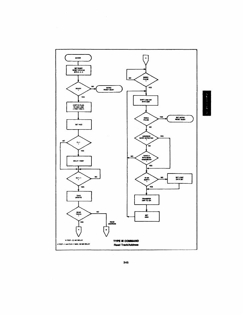
.. TEST- •• NOOElAY
.TEST-I .... CU<-IIIIIZ.30 .. OElAY
III1RQ RESET as\'
345

RESETIUSY SET INTAO SETRNF
TYPE 10 COMMAND Read Track/Address
TYPE IV COMMAND
FORCE INTERRUPT
This command can be loaded into the command regist~r at any time. If there is a current command under execution (Busy Status Bit set), the command will be terminated and an interrupt will be generated when the condition specified in ·the 10 through 13 field is detected. The interrupt conditions are shown below:
10 = Not-Ready-To-Ready Transition 1, = Ready-To-Not~Ready Transition 12 = Every Index Pulse b = Immediate Interrupt (requires reset, see
Note) NOTE: If 10 - 13 = 0, there is no interrupt generated but
the current command is terminated and busy is reset. This is me only command that will enable the immediate interrupt to clear on a subsequent Load Command Register or Read Status Register.
STATUS DESCRIPTION Upon receipt of any command, except the Force Interrupt command, the Busy Status bit is set and the rest of the status bits are updated or cleared for the new command. If the Force Interrupt Command is received when there is a current command under execution, the Busy status bit is reset, and the rest of the status bits are unchanged. If the Force Interrupt command is received when there is not a current command under execution, the Busy Status bit is reset and the rest of the status bits are updated or cleared. In this case, Status reflects the Type I commands.
The format of the Status Register is shown below:
Status varies according to the type of command executed as shown in Table 6.
346

FORMATTING THE DISK
(Refer to section on Type III commands for flow diagrams.)
Formaning the disk is a relatively simple task when operating programmed 1/0 or when operating under Formaning the disk is accomplished by positioning the R/W head oyer the desired track number and issuing the Write Track command. Upon receipt of the Write Track command, the FD179X raises the Data Request Signal. At this point in time, the user loads the data register with desired data to be written on the disk. For every byte of information to be written on the ·disk, a data request is generated. This sequence continues from one index mark to the next index mark. Normally, whatever data pattern appears in the data register is written on the disk with a normal clock panern. However, if the F0179X detects a data pattem of F5 thru FE in the data register, this is interpreted as data address marks with missing clocks or CRC generation. For instance, in FM an FE panern will be interpreted as an 10 address mark (DATA-FE, CLK-C7) and the CRC will be initialized. An F7 panern will generate two CRC characters in FM or MFM. As a consequence, the panems F5 thru FE must not appear in the gaps, data fields. or 10 fields. Also, CRe's must be generated by an F7 pattern. Disks may be formatted in IBM 3740 or System 34 formats with sector lengths of 128. 256, 512, or 1024 bytes.
."..,,~otooGC~OC. ,-..,.s.'oQItII
.'M( ... 't~ •• I1110~ ¥<SS-.GCIOClit ' • .ues.',01'10 .... , .... ''\\a..o.
IBM 3740 FORMAT-128 BYTESISECTOR
Shown below is the IBM single-density format with 128 bytes/sector. In order to format a diskette. the user must issue the Write Track command, and Ioac the data register with the following values. For eve!') byte to be written, there is one data request.
NUMBER HEX VALUE OF OF BYTES BYTE WRITTEN
40 FF (or 00)' 6 00 1. FC (Index Mark)
26 FF (or 00) 6 00 1 FE (10 Address Mark) 1 Track Number 1 Side Number (00 or 01) 1 Sector Number (1 thru lA) 1 00 f. F7 (2 CRC's wrinen)
11 FF (or 00) 6 00 t FB (Data Address Mark)
126 Data (IBM uses E5) 1 F7 (2 CRC's written)
27 FF (or 00) 247" FF (or 00)
·Write bracketed field 26 times
**Continue writing until F0179X interrupts out. Approx. 247 bytes.
l-Optional '00' on 1795/7 only .
11M TRACK FORMAl.
347

1_ SYSTEM 34 FORMAT-256 BYTESISECTOR Shown below is the IBM dual-density format with 256 bytes/sector. In order to format a diskette the user must issue the Write Track command and load the data register with the following values. For every byte to be written, there is one data request.
NUMBER HEX VALUE OF OF BYTES BYTE WRITTEN
80 4E 12 00 3 F6 1 FC (Index Mark) . 4E
12 00 3 F5 1 FE (10 Address Mark) 1 Track Number (0 thru 4C) 1 Side Number (0 or 1) 1 Sector Number (1 thru 1A) 1 01 1 F7 (2 CRCs written)
22 4E 12 00 3 F5 1 FB (Data Address Mark)
256 DATA 1 F7 (2 CRCs written) ~ 4E
598·- 4E
• Write bracketed field 26 times --Continue writing until FD179X interrupts out.
Approx. 598 bytes.
ELECTRICAL CHARACTERISTICS MAXIMUM RATINGS
1. NON-IBM FORMAlS
Variations in the IBM format are possible to a Iimit~ extent if the following requirements are met: sector size must be a choice d 128, 256, 512, or 1024 bytes; gap size must be according to the following table. Note that the Index Mark Is not required by the 179X. The minimum gap sizes shown are that which Is required by the 179X, with PLL Iock-up time, motor speed variation, etc., adding additional bytes.
FM MFM
Gap I 16 bytes FF 32 bytes4E
Gap II 11 bytes FF 22 bytes4E
. 6 bytes 00 12 bytes 00 3 bytesA1
Gap III 10 bytes FF 24 bytes4E 3 bytesA1
.- 4 bytes 00 8 bytes 00
Gap IV 16 bytes FF 16 bytes4E
-Byte counts must be exact . --Byte counts are minimum, except exactly 3 bytes
of A 1 must be written.
Voo With Respect to Vss (Ground) =15 to -0.3V Max. Voltage to Any Input With =15 to -0.3V
Respect to Vss
Operating Temperature Storage Temperature
OOC to 700c -55°C to +1250C
VOD = 10 ma Nominal VCC = 35 rna Nominal
OPERATING CHARACTERISTICS (DC) TA = O"C to 7O"C. Voo = + 12V ± .6V, Vss = OV. Vee = + 5V ± .25V
SYMBOL CHARACTERISTIC MIN. MAX. UNITS CONDITIONS III Input Leakage 10 p.A V". = Voo 101. Output Leakage 10 p.A VOOT = Voo VVH Input High Voltage 2.6 V VIL Input low Voltage 0.8 V
VCY>I Output High Voltage 2.8 V 10 = -100 p.A VOl Output Low Voltage 0.45 V 10 = 1.6 rnA Po Power Dissipation 0.5 W
348

nlllNG CHARACTERISTICS
TA = OOC to 700c. Voo = + 12V ± .6V. Vss = OV. Vee =+5V ± .25V
READ ENABLE 'OMINO
SYMBOL TSET THLD TRE TORR TIRR TDACC TOOH
CHARACTERISTIC MIN. TYP.
Setup ADOR & CS to ~ 59 Hold ADDR & CS from FiE 10 RE Pulse Width 400 ORa Reset from RE 400 INTRa Reset from RE 500 Data Access from RE Data Hold From RE 50
III' ---+---.
,1!AlO ---t-----t
IiIIOTI , B ••• "...,.....'lY'.OlOW"DlS .. O ." .. DOUafS ..... aocc 'UH.
!~AV;~~ ~~ST CASEI
'UF .. '3SuS
READ EMABLE 'OMiNO
349
MAX. UNITS CONDITIONS
nsec nsec nsec CA.=50pf
500 nsec 3000 nsec See Note 5 350 nsec CA.=50pf 150 nsec CA.=50pf
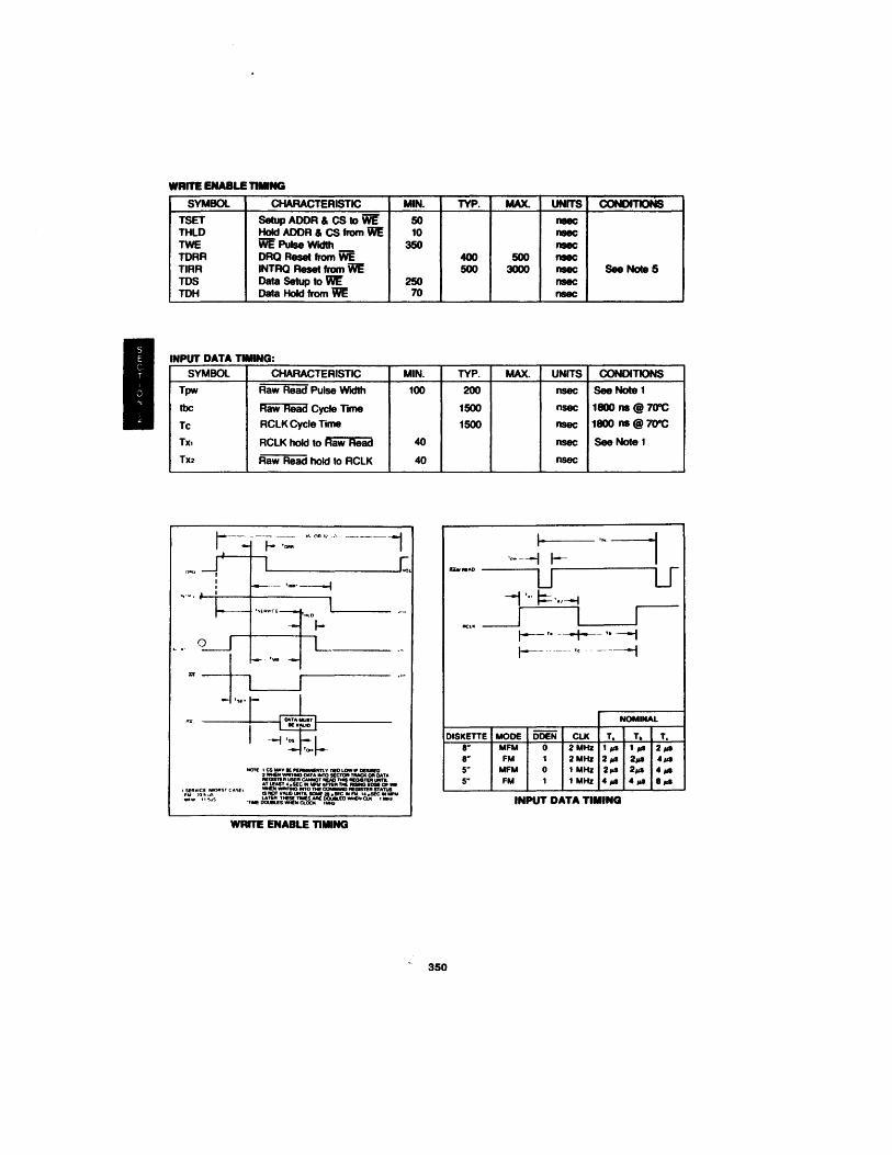
WRITE ENABLE TIMING
SYMBOl CHARACTERISTIC MIN. TYP. MAX. UNITS CONDITIONs TSET Setup ADDR & CS to WE 50 nsec THLO Hold ADOR & CS from ~ 10 nsec TWE WE Pulse Width 350 nsec TORR ORO Reset from WE 400 500 nsec TIRR INTRQ Reset from ~ 500 3000 nsec See Note 5 TOS Data Setup to \W 250 nsec TDH Data Hold from ~ 70 nsec
INPUT DATA nMlNG: SYMBOL CHARACTERISTIC MIN. TYP. MAX. UNITS CONDITIONS
Tpw Raw Read Pulse Width 100 200 "sec See Note 1
tbc Raw Read Cycle Time 1500 "sec 1800 ns @ 7O"C
Tc RCLK Cycle Time 1500 nsec 1800 ns @ 7O"C
TXl RCLK hold to Raw Read 40 "sec See Note 1
TX2 Raw Read hold to RCLK 40 "sec
I '~I ' •• -----I ~ iiw .. AO
U Lf -1'" t:=,.,~
I I lieU
t--'. ---t---"-1 1-- 'c -- ----I
NOMINAL
OISKETTE MODE DDEN elK T. T. Tc 8" MFM 0 2 MHz 1,.. 1,.. 2,.. 8" FM 1 2 MHz 2,.. 2,.. 4,.. 5" MFM 0 1 MHz 2,.. 2,.. 4,.. 5" FM 1 1 MHz 4,.. 4,.. 8,..
INPUT DATA TIMING
WRITE ENABLE nlllNG
350
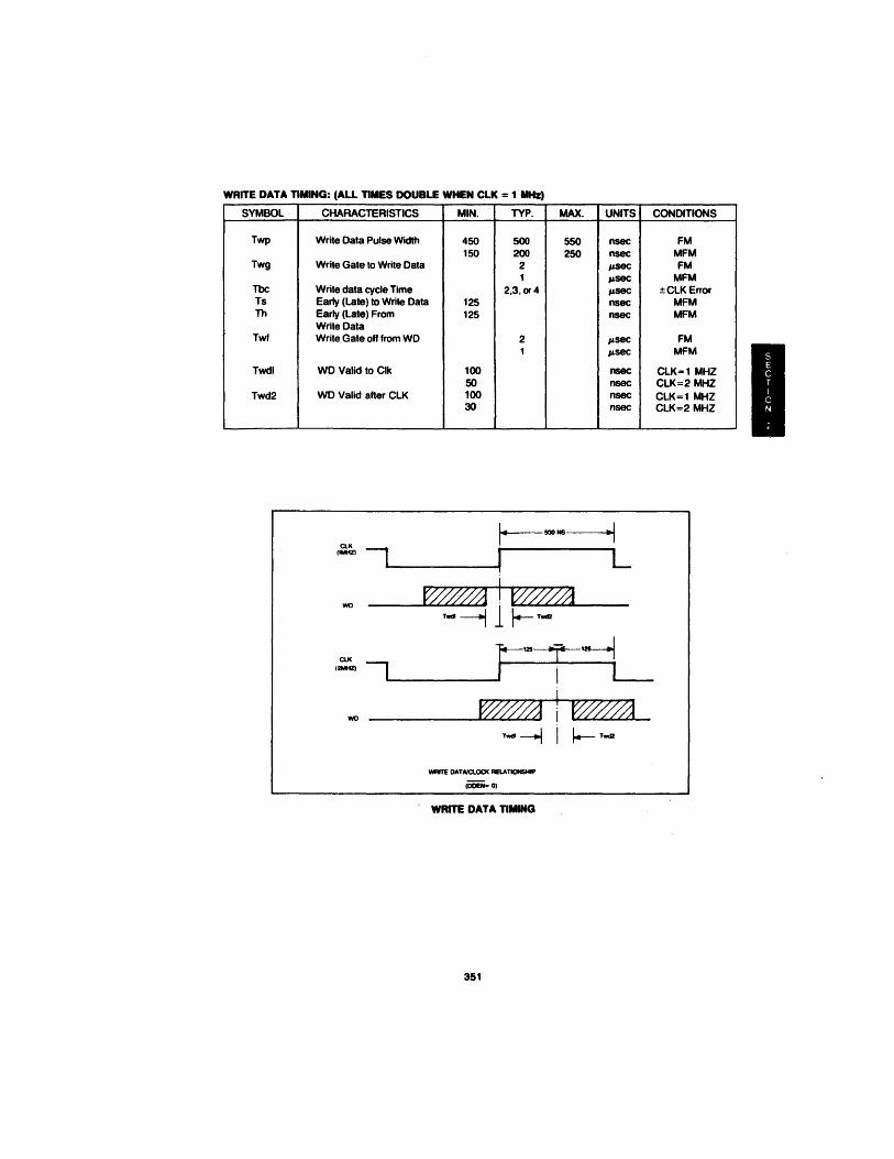
WRITE DATA nMlNG: (ALL nMES DOUBLE WHEN eLK = 111Hz)
SYMBOL
Twp
Twg
Tbc Ts Th
Twf
Twdl
Twd2
CHARACTERISTICS MIN. TYP. MAX.
Write Data Pulse Width 450 500 550 150 200 250
Write Gate to Write Data 2 1
Write data cycle Time 2,3, or4 Early (Late) to Write Data 125 Early (late) From Write Data Write Gate off from WD
WD Valid to Clk
WD Valid after CLK
ClK IIMHZ!
WD
ClJ(
(2MHZ)
we
I
125
2 1
100 50 100 30
r---, ~4 IW/p~
Twd! ---i 1 ~Twd2
WRITE DATA/ClOClC AElATlONSHIP
(OOEN- 0)
WAITE DATA nMING
351
UNITS CONDITIONS
nsec FM nsec MFM
"sec FM
"sec MFM p.S8C ±ClKError nsec MFM nsec MFM
"sec FM
"sec MFM
nsec ClK=1 MHZ nsec CLK=2 MHZ nsec ClK=1 MHZ nsec CLK=2 MHZ
~I
L

MISCELLANEOUS nMING:
SYMBOL CHARACTERISTIC MIN. TYP. MAX. UNITS CONDITIONS
TCD, Clock Duty (low) 230 250 20000 nsec TCDtI Clock Duly (high) 200 250 20000 nsec TSTP Step Pulse Output 201'4 p.sec See Note 5 TDIR Dir Setup to Step 12 p.sec ±CLKERROR TMA Master Reset Pulse Width 50 p.sec TIP Index Pulse Width 10 p.sec See Note 5 TWF Write Fault Pulse Width 10 p.sec
;;; j f , ..
I---- ',p---I w' I I I J ""
1----'". ~ ;;; J I I 1 ""
1---- ,- -I
,00< ~"'P'" f~L..--_ 'Ol 1-.o,.-l'''.I----l'''.~ I-"".-j"'pl-
~~ MISCELLANEOUS TIMING
NOTES: 1. Pulse width on RAW READ (Pin 27) is normally
100-300 ns. However. pulse may be any width if pulse is entirely within window. If pulse occurs in both windows. then pulse width must be less than 300 ns for MFM at CLK = 2 MHz and 600 ns for FM at 2 MHz. Tmes double for 1 MHz.
3. tbc should be 2 p.S, nominal in MFM and 4 p's nominal in FM. Times double when CLK = 1 MHz.
2. A PPL Data Separator is recommended for 8" MFM.
4. RCLK may be high or low during RAW READ (Polarity is unimportant).
5. Times double when clock = 1 MHz.
352

WESTERN DIGITAl. c o R P 0 R A T I o N
FD179X Application Notes
INTRODUCTION
Over the past several years, the Aoppy Disk Drive has become the most popular on-line storage device for mini and microcomputer systems. Its fast access time, reliability and low cost-per-bit ratio enables the Floppy Disk Drive to be the solution in mass storage for microprocessor systems. The drive interface to the Host system is standardized, allowing the OEM to substitute one drive for anotl}er with minimum hardwareJ software modifications.
Since Floppy Disk Data is stored and retrieved as a self-clocking serial data stream, some means of separating the clock from the data and assembling this data in parallel form must be accomplished. Data is stored on individual Tracks of the media, requiring control of a stepper motor to move the ReadlWrite head to a predetermined Track, Byte sychronization must also be accomplished to insure that the parallel data is properly assembled. After all the design considerations are met, the final controller can consist of 40 or more TTL packages.
To alleviate the burden of Floppy Disk Controller design, Western Digital has developed a Family of LSI Floppy Disk controller devices. Through its own set of macro commands, the FD179X Controller Family will perform all the functions necessary to read and write data to the drive. Both the 8" standard and 5114" minifloppy are supported with single or double density recording techniques. The FD179X is compatible with the IBM 3740 (FM) data format, or the System 34 (MFM) standards. Provisions for non-standard formats and variable sector lengths have been induded to provide more storage capability per track. Requiring standard +5, +12 power supplies the FD179X is available in a standard 40 pin dual-in-line package.
The FD179X Family consists of 6 devices. The differences between these devices is summarized in Figure 1. The 1792 and 1794 are "single density only" devices, with the Double Density Enable pin (DDEN) left open by the user. Both True and inverted Data bus devices are available. Since the 179X can only drive one TTL Load, a true data bus system may use the 1791 with external inverting buffers to arrive at a true bus scheme. The 1795 and 1797 are identical to the 1791 and 1793, except a side select output has been added that is controlled through the command Register.
I Ii ... III
SYSTEM DESIGN \I >
The first consideration in Aoppy Disk Design is to de- i termine which type of drive to use. The choice ranges from single-density single sided mini-ftoppy to the 8" double-density double-sided drive. Figure 2 illustrates the various drive and data capacities associated with each type. Although the 8" doubJe..density drive offers twice as much storage, a more complex data separator and the addition of Write Precompensation circuits are mandatory for reliable data transfers. Whether to go with 8" double-density or not is dependent upon PC board space and the additional circuitry needed to accurately recover data with extreme bit shifts. The byte transfer time defines the nominal time required to transfer one byte of data from the drive. " the CPU used cannot service a byte in this time, then a DMA scheme will probably be required. The 179X also needs a few microseconds for overhead, which is subtracted from the transfer time. Figure 3 shows the actual service times that the CPU must provide on a byte-by-byte basis. "these times are not met, bytes of data win be lost during a read or write operation. For each byte transferred, the 179X generates a ORO (Data Request) signal on Pin 38. A bit is provided in the status register which is also set upon receipt of a byte from the Disk. The user has the option of reading the status register through program control or using the ORO Une with DMA or interrupt schemes. When the data register is read, both the status register ORO bit and the ORO Une are automatically reset. The next full byte will again set the ORO and the process continues until the sector(s) are read. The Write operation works exadly the same way, except a WRITE to the Data Register causes a reset of both ORa's.
RECORDING FORMATS
The FD179X accepts data from the disk in a Frequency-Modulated (FM) or Modified-Frequency-Modulated (MFM) Format. Shown in Figures 4A and 4B are both these Formats when writing a Hexidecimal byte of '02'. In the FM mode, the 8 bits of data are broken up into "bit cells." Each bit cel begins with a clock pulse and the center of the bit cell defines the data. H the data bit = 0, no pulse is written; if the data = 1, a pulse is written in the center of the cell. For the 8" drive, each clock is written 4 microseconds apart.
355

In the MFM mode, clocks are decoded into the data stream. The byte is again broken up into bit cells, wtth the data bit written in the center of the bit cell if data = 1. Clocks are only written if both surrounding data bits are zero. Figure 4B shows that this occurs only once between Bit cell 4 and 5. Using this encoding scheme, pulses can occur 2, 3 or 4 microseconds apart. The bit cell time is now 2 microseconds; twice as much data can be recorded without increasing the Frequency rate due to this encoding scheme.
The 179X was designed to be compatible with the IBM 3740 (FM) and System 34 (MFM) Formats. Although most users do not have a need for data exchange with IBM mainframes, taking advantage of these well studied formats will insure a high degree of system performance. The 179X will allow a change in gap fields and sector lengths to increase usable storage capacity, but variations away from these standards is not recommended. Both IBM standards are soft-sector format. Because of the wide variation in address marks, the 179X can only support soft-sectored media. Hard sectored diskettes have continued to lose popularity, mainly due to the unavailability of a standard and the limitation of sector lengths imposed by the physical sector holes in the diskette.
PROCESSOR INTERFACE
The Interface of the 179X to the CPU consists of an 8-bit Bi-directional bus, read/write controls and optional interrupt lines. By selecting the device via the CHIP SELECT Une, each of the five internal registers can be accessed.
Shown below are the registers and their addresses:
PIN 3 PIN 6 PIN 5 PIN 4 PIN 2 CS A1 Ao RE=d WE-4
0 0 I 0 STATUS REG COMMAND REG
0 0 1 TRACK REG TRACK REG 0 1 0 SECTOR REG SECTOR REG 0 1 1 DATA REG DATA REG 1 X X H1-Z H1-Z
Each time a command is issued to the 179X, the Busy bit is set and the INTRa (Interrupt Request) Une is reset. The user has the option of checking the busy bit or use the INTRa Une to denote command completion. The Busy bit will be reset whenever the 179X is idle and awaiting a new command. The INTRa Une,. once set, can only be reset by a READ of the status register or issuing a new command. The MR (Master Reset) Une does not affect INTRa.
The P.o, A1, Unes used for register selections can be configured at the CPU in a variety of ways. These lines may actually tie to CPU address lines, in which case the 179X will be memory-mapped and addressed like RAM. They may also be used under Program Control by tying toa port device such as the 8255, 6820, etc. As a diagnostic tool when checking out the CPU interface, the Track and Sector registers should respond like "RAM" when the 179X is idle (Busy = INTRa = 0).
Because of internal synchronization cycles, certain time delays must be introduced when operating under Programmed I/O. The worst case delays are:
PERATION NEXT OPERATION
DELAY REO'
READ STATUS MFM = 141Ls· REGI~TER ___ FM = 28ILs. __
RITE TO READ FROM A NO DELAY Y REGISTER DIFFERENT REG
·NOTE: Times Double when CLK = 1MHz (5Y4" drive)
Other CPU interface lines are CLK, MR and DDEN. The ClK line should be 2MHz (8" drive) or 1MHz (5V4" drive) with a 50% duty cycle. Accuracy should be ±1% (crystal source) since all internal timing, including stepping rates, are based upon this clock.
The MR or Master Reset Une should be strobed a minimum of 50 microseconds upon each power-on condition. This line clears and initializes all intemal registers and issues a restore command (Hex '03') on the rising edge. A quicker steppinQE!te can be written to the command register after a MR, in which case the remaining steps will occur at the faster programmed rate. The 179X will issue a maximum of 255 stepping pulses in an attempt to expect the TROO line to go active low. This line should be connected to the drive's TROO sensor. The DDEN line causes selection of either single density (DDEN = 1) or double density operation. DDEN should not be switched during a read or write operation.
356

FLOPPY DISK INTERFACE
The Floppy Disk Interface can be divided into three sections: Motor Control, Write Signals and Read Signals. All of these lines are capable of driving one TTL load and not compatible for direct connection to the drive. Most drives require an open-collector TTL interface with high current drive capability. This must be done on all outputs from the 179X. Inputs to the 179X may be buffered or tied to the Drives outputs, providing the appropriate resistor termination networks are used. Undershoot should not exceed -0.3 volts, while integrity of V1H and VOH levels should be kept within spec.
MOTOR CONTROL
Motor Control is accomplished by the STEP and DIRC lines. The STEP Une issues stepping pulses with a period defined by the rate field in all Type I commands. The DIRC line defines the direction of steps (DIRC = 1 STEP IN/DiRC = 0 STEP OUT).
Other Control lines include the iP or Index Pulse. This line is tied to the drives' Index l.E.D. sensor and makes an active transition for each revolution of the diskette. The TROO Une is another l.E.D. sensor that informs the 179X that the stepper motor is at its furthest position, over Track 00. The READY line can be used for a number of functions, such as sensing "door open", Drive motor on, etc. Most drives provide a programmable READY Signal selected by option jumpers on the drive. The 179X will look at the ready signal prior to executing READ/WRITE commands. READY is not inspected during any Type I commands. All Type I commands will execute regardless of the logic level on this line.
WRITE SIGNALS
Writing of data is accomplished by the use of the WD, WG, WF, TG43, EARLY and LATE lines. The WG or Write Gate line is used to enable write current at the drive's R/W head. It is made active prior to writing data on the disk? The WF or WRITE FAULT line is used to inform the 179X of a failure in drive electronics. This signal is multiplexed with the VFOE line and must be logically separated if required. Figure 5 illustrates three methods of demultiplexing.
The TG43 or "TrACK GREATER than 43" line is used to decrease the Write current on the inner tracks, where bit densities are the highest. If not required on the drive, TG43 may be left open.
WRITE PRECOMPENSATION
The 179X provides three signals for double density Write Precompensation use. These signals are WRITE DATA, EARLY and LATE. When using single density drives (eighter 8" or 511."), Write Precompensation is not necessary and the WRITE DATA line is generally TTL Buffered and sent directly to the drive. In this mode, EARLY and LATE are left open. For double density use, Write Precompensation is a function of the drive. Some manufacturers recommend Precompensating the 511." drive, while others do not. With the 8" drive, Precompensation may be specified from TRACK 43 on, or in most cases, all TRACKS. If the recommended Precompensation is not specified,
357
check with the manufacturer for the proper configuration required.
The amount of Precompensation time also varies. A typical value will usually be specified from 1 QO-3OOns. Regardless of the parameters used, Write Precornp80ENtion must be done external to the 179X. When o is tied low, EARLY or LATE will be activated at least 125os. before and after the Write Data pulse. An Algorithm internal the 179X decides whether to raise EARLY or LATE, depending upon the previOUS bit pattern sent. As an example, suppose the recommended Precomp value has been specified at 150ns. The following action should be taken:
EARLY
o o 1
LATE ACTION TAKEN
o delay WD by 150ns (nominal) 1 delay WD by 300ns (2X value) o do not delay WD
There are two methods of performing Write Precompensation:
1) External Delay elements 2) Digitally
Shown in Figure 6 is a Precomp circuit using the Western Digital 2143 clock generator as the delay element. The WD pulse from the 179X creates a strobe to the 2143, causing subsequent output pulses on theA1,,(1'2 and .03 signals. The 5K Precomp adjust sets the desired Precomp value. Depending upon the condition of EARLY and LATE,.9'1 will be used for EARLY, iI2 for nominal (EARLY = LATE = 0), and B3 for LATE. The use of "one-shots" or delay line in a Write Precompensation scheme offers the user the ability to vary the Precomp value. The /lI4 output resets the 74LS175 Latch in anticipation of the next WD pulse. Figure 7 shows the WD-EARL Y/LA TE relationship, while Figure 8 shows the timing of this write Precomp scheme.
Another method of Precomp is to perform the function digitally. Figure 9 illustrates a relationship between the WD pulse and the CLK pin, allowing a digital Precomp scheme. Figure 10 shows such a ~heme with a preset Write Precompensation value of 250ns. The synchronous counter is used to generate 2MHz and 4MHz clock signals. The 2M Hz clock is sent to the CLK input of the 179X and the 4MHz is used by the 4-bit shift register. When a WD pulse is not present, the 4MHz clock is shifting "ones" through the shift register and maintaining Q o at a zero level. When a WD pulse is present, a zero is loaded at either A, B, or C depending upon the states of LATE, EN PRECOMP and EARLY. The zero is then shifted by the 4MHz clock until it reaches the Qo output. The number of shift operations determines whether the WRITE DATA pulse is written early, nominal or late. If both FM and MFM operations is a system reqUirement, the output of this circuit should be disabled and the WD pulse should be sent directly to the drive.

DATA SEPARATION The 179X has two inputs (RAW READ & RCLK) and one output (VFOE) for use by an external data separator. The RAW READ input must present clock and data pulses to the 179X, while the RCLK input provides a "window" or strobe signal to clock each RAW READ pulse into the device. An ideal Data Separator would have the leading edge of the RAW READ pulse occur in the exact center of the RCLK strobe.
Motor Speed Variation, Bit shifts and read amplifier recovery circuits a/l cause the RAW READ pulses to drift away from their nominal positions. As this occurs, the RAW READ pulses will shift left or right with respect to RCLK. Eventually, a pulse will make its tran· sition outside of its RCLK window, causing either a CRC error or a Record-not-Found error at the 179X.
A Phase-Lock-Loop circuit is one method of achieving synchronization between the RCLK and RAW READ signals. As RAW READ pulses are fed to the PLl, minor adjustments of the free-running RClK frequency can be made. If pulses are occurring too far apart, the RClK frequency is decreased to keep synchronization. If pulses begin to occur closer together, RClK is increased until this new higher frequency is achieved. In normal read operations, RClK will be constantly adjusted in an attempt to match the incoming RAW READ frequency.
Another method of Data Separation is the CounterSeparator technique. The RClK signal is again freerunning at a nominal rate, until a RAW READ pulse occurs. The Separator then denotes the pOsition of the pulse with respect to RClK (by the counter value), and counts down to increase or decrease the current RClK window. The next RClK window will occur at a nominal rate and will continue to run at this frequency until another RAW READ pulse adjusts RCLK, but only the present window is adjusted.
Both PPl and Counter/Separator are acceptable methods of Data Separation. The PPl has the highest reliability because of its "tracking" capability and is recommended for 8" double density deSigns.
As a final note, the term "Data Separator" may be misleading, since the physical separation of clock and data bits are not actually performed. This term is used throughout the industry, and can better be described as a "Data Recovery Circuit" rather than a Data Separator. The VFOE signal is an output from the 179X that signifies the head has been loaded and valid data pulses are appearing on the RAW READ line. It can be used to enable the Data Separator and to insure clean RClK transitions to the 179X. Since some drives will output random pulses when the head is disengaged, VFOE can prevent an erratic RClK signal during this time. If the Data Separator requires synchronization during a known pattern of one's or zero's, then RG (READ GATE) can be used. The RG signal will go active when the 179X is currently over a field of zeros or ones. RG is not available on the 1795/1797 devices, since this signal was replaced with the SSO (Side Select Output) Line.
Shown in Figure 11 is a 2112 IC Counter/Separator. The 74lS193 free runs at a frequency determined by the CRYClK input. When a RAW READ pulse occurs, the counter is loaded with a starting count of '5'. When the RAW READ Line returns to a logic 1, the counter counts down to zero and again free runs. The 74lS74 insures a 50% duty cycle to the 179X and performs a divide-by-two of the aD output.
Figure 12 illustrates another Counter/Separator utilizing a PROM as the count generator. Depending upon the RAW READ phase relationship to RCLK, the PROM is addressed and its data output is used as the counter value. A 16MHz clock is required for 8" double density, while an 8M Hz clock can be used for single density.
Figure 13 shows a Phase-lock-loop data recovery circuit. The phase detector (U2, Figure 2) compares the phase of the SHAPED DATA pulse to the phase of VFO ClK + 2. If VFO ClK -T 2 is lagging the SHAPED DATA pulse an output pulse on #9, U2 is generated. The filter/amplifier converts this pulse into a DC signal which increases the frequency of the VCO. If, correspondingly, ClK + 2 is leading the SHAPED DATA pulse, an output pulse on #5, U2 is generated. This pulse is converted into a DC signal which decreases the frequency of the VCO. These two actions cause the VCO to track the frequency of the incoming READ DATA pulses. This correction process to keep the two signals in phase is constantly occurring because of spindle speed variation and circuit parameter variations. The operating specifications for this circuit are as follows:
Free Running Frequency 2MHz Capture Range ± 15% lock Up lime 50 microsec." 1111" or
"0000" Pattern 100 Microsec "1010" Pattern
The RAW READ pulses are generated from the falling edge of the SHAPED DATA pulses. The pulses are also reshaped to meet the 179X requirements. VFO ClK + 2 OR 4 is divided by 2 once again to obtain VFO ClK OUT whose frequency is that required by the 179X RClK input. RClK must be controlled by VFOE so VFOE is sampled on each rising edge of VFO ClK OUT. When VFOE goes active EN RCLK goes active in synchronization with VFO CLK OUT preventing any glitches on the RClK output. When VFOE goes inactive EN RClK goes inactive in synchronization with VFO ClK OUT, again preventing any glitches on the RClK output.
Figure 14 illustrates a PPl data recovery circuit using the Western Digital 1691 Floppy Support device. Both data recovery and Write Precomp logic is contained within the 1691, allowing low chip count and Pll reliability. The 74S124 supplies the free-running VCO output. The PUMP UP and PUMP DOWN signals from the 1691 are used to control the 745124's frequency.
358
COMMAND USAGE Whenever a command is successfully or unsuccessfuRy completed, the busy bit of the status register is reset and the INTRa line is forced high. Command termination may be detected either way. The INTRa can be tied to the host processor's interrupt with an appropriate service routine to terminate commands. The busy bit may be monitored with a user program and will achieve the same results through software. Performing both an INTRQ and a busy bit check is not recommended because a read of the status register to determine the condition of the busy bit will reset the INTRa line. This can cause an INTRa from not occurring.
RESTORE COMMAND
On some disk drives, it is possible to position the R/W head outward past Track 00 and prevent the TROO line from going low unless a STEP IN is first performed. If this condition exists in the drive used, the RESTORE command will never detect a TROO. Issuing several STEP IN pulses before a RESTORE command will remedy this situation. The RESTORE and all other Type I commands will execute even though the READY bit indicates the drive is not ready (NOT READY = 1).
READ TRACK COMMAND The READ TRACK command can be used to manually inspect data on a hard copy printout. Gaps, address marks and a" data are brought in to the data register during this command. The READ TRACK command may be used to inspect diskettes for valid formatting and data fields as well as address marks. Since the 179X does not synchronize clock and data until the Index Address Mark is detected, data previous to this 10 mark will not be valid. READ GATE (RG) is not actuated during this command.
READ ADDRESS COMMAND
In systems that use either multiple drives or sides, the read address command can be used to tell the host processor which drive or side is selected. The current position of the R/W head is also denoted in the six bytes of data that are sent to the computer.
ITRACK SIDE I SECTOR I LE~~TH I C~C I C~C I The READ ADDRESS command as well as all other Type II and Type III commands wi" not execute if the READY line is inactive (READY = (I). Instead, an interrupt will be generated and the NOT READY status bit will be set to a 1.
FORCED INTERRUPT COMMAND
The Forced Interrupt command is generally used to terminate a multiple sector command or to insure Type I status in the status register. The lower four bits of the command determine the conditional interrupt as follows:
359
10 NOT-READY TO READY TRANSITION 1, READY TO NOT-READY TRANSITION 12 EVERY INDEX PULSE 13 IMMEDIATE INTERRUPT
Regardless of the conditional interrupt set, any command that is currently being executed when the Forced Interrupt command is loaded will immediately be terminated and the busy bit will be reset indicating an idle condition.
Then, when the condition for interrupt is met, the INTRa line will go high signifying that the condition specified has occurred.
The conditional interrupt is enabled when the corresponding bit positions of the command (13 -10) are set to a 1. If 13 -10 are all set to zero, no interrupt will occur, but any command presently under execution will be immediately terminated upon receipt of the Force Interrupt command (HEX 00). As usual, to clear the interrupt a read of the status register or a write to the command register is required. The exception is when using the immediate interrupt condition (13 = 1). If this command is loaded into the command register, an interrupt will be immediately generated and the current command terminated. Reading the status or writing to the command register will not automatically clear the interrupt; another forced interrupt command with 13 -10 = 0 must be loaded into the command register in order to reset the INTRa from this condition.
More than one condition may be set at a time. H for example, the READY TO NOT-READY condition (I, = 1) and the Every Index Pulse (12 = 1) are both set, the resultant command would be HEX "DA". The "OR" function is performed so that either a READY TO NOTREADY or the next Index Pulse will cause an interrupt condition.
DATA RECOVERY Occasionally, the R/W head of the disk drive may get "off track", and dust or dirt may get trapped on the media. Both of these conditions will cause a RECORD NOT FOUND andlor a CRC error to occur. This "soft error" can usually be recovered by the following procedure:
1. Issue the command again 2. Unload and load the head and repeat step 3. Issue a restore, seek the track, and repeat step 1
If RNF or CRC errors are still occurring after trying these methods, a "hard error" may exist. This is usually caused by improper disk handling, exposure to high magnetic fields, etc. and generaHy results in destroying portions or tracks of the diskette.

FIGURE 1 DEVICE CHARACTERISTICS
DEVICE SNGl DENSITY DBlE DENSITY INVERTED BUS TRUE BUS DOUBLE-SIDED
1791 X X X 1792 X X 1793 X X 1794 X 179S X X X 1797 X X
FIGURE 2 STORAGE CAPACITIES
UNFORMATTED CAPACITY (NOMINAL)
SIZE DENSITY SIDES PER TRACK PER DISK
SV4" SINGLE 1 3125 109,37S" SV4" DOUBLE 1 6250 218,750 5V4" SINGLE 2 3125 218,750 5W' DOUBLE 2 6250 437,500 8" SINGLE 1 5208 401,016 8" DOUBLE 1 10,416 802,032 8" SINGLE 2 5208 802,032 8" DOUBLE 2 10,416 1,604,064
"Based on 35 Tracks/Side ""Based on 18 Sectors/Track (128 byte/sec)
""·Based on 18 Sectors/Track (256 bytes/sec)
360
X X
X X X
FORMATTED BYTE CAPACITY
TRANSFER TIME PER TRACK PER DISK
64#1-s 2304"" 80,640 32#1-s 4608""" 161,280 64#1-s 2304 161,280 32#1-s 4608 322,560 32#1-8 3328 256,256 16#1-s 6656 512,512 32#1-s 3328 512,512 16#1-S 6656 1,02S,024
11.5 Appendex E - Z80A CPU ••••••••••••••••••

Featur ..
200i 0210. 0211
• The instruction set contains 158 instructions. The 78 instructions of the 8080A are included as a subset; 8080A software compatibility is maintained.
• Six MHz, 4 MHz and 2.5 MHz clocks for the zaOB, zaOA, and zao CPU result in rapid instruction execution with consequent high data throughput.
• The extensive instruction set includes string, bit, byte, and word operations. Block searches and block transfers together with indexed and relative addressing result in the most powerful data handling capabilities in the microcomputer industry.
• The zao microprocessors and associated family of peripheral controllers are linked by a vectored interrupt system. This system
.v.,.... ! COIITROL
CPU ! COIITROL
CPU { .US CONTROL
iiREO
IORO
RD
WI!
RFSH
ZIOCPU
Figure 1. Pin Functions
Z8400 zaer CPU Cealral Proc ..... , U.II
Product SpecUlcalloa
March 1981
may be daisy-chained to allow implementation of a priority interrupt scheme. Little, if any, additional logic is required for daisy-chaining.
• Duplicate sets of both general-purpose and flag registers are provided, easing the design and operation of system software through single-context SWitching, background-foreground programming, and Single-level interrupt processing. In addition, two 16-bit index registers facilitate program processing of tables and arrays.
• There are three modes of high speed interrupt processing: 8080 compatible, non-zaO peripheral deVice, and zao Family peripheral with or without daisy chain.
• On-chip dynamic memory refresh counter.
Au ~ 1
A12 ~ 2
A .. ~ 3
A,. ~ 4 A,s _ 5
elK ~ 8
D. 1
D3 8
D. 9
0,. 10
+5V 11
0. 12
Dr [ 13
Do 14
Dl 15
iNT 18
iiiii 11
HID 18
~ 19
iOiiO 20
Z80CPU
40 A,.
39 '" 38 As 37 A7
38 '" 35 As
34 As 33 A3
32 A.
31 A,
30 Ao 211 GND
28 ~ IWSH 21 ~ iii
2825 ~ REm .. IUSREO
2324 ~]WAiT
iUSACi 22bJWii 21 D iiii
~---.....
Figure 2. Pin Assignments
5
I 9

General Description
6
The Z80, Z80A, and Z80B CPUs are thirdgeneration single-chip microprocessors with
. exceptional computational power. They offer higher system throughput and more efficient memory utilization than comparable secondand third-generation microprocessors. The internal registers contain 208 bits of read/write memory that are accessible to the programmer. These registers include two sets of six generalpurpose registers which may be used individually as either 8-bit registers or as 16-bit register pairs. In addition, there are two sets of accumulator and flag registers. A group of "Exchange" instructions makes either set of main or alternate registers accessible to the programmer. The alternate set allows operation in foreground-background mode or it may
+SY __
GND __
CLOCK __
be reserved for very fast interrupt response. The Z80 also contains a Stack POinter, Pro
gram Counter, two index registers, a Refresh register (counter), and an Interrupt register. The CPU is easy to incorporate into a system since it requires only a single + 5 V power source, all output signals are fully decoded and timed to control standard memory or peripheral circuits, and is supported bran extensive family of peripheral controllers. The internal block diagram (Figure 3) shows the primary functions of theZ80 processors. Subsequent text provides more detail on the Z80 I/O controller family, registers, instruction set, interrupts and daisy chaining, and CPU timing.
Figure 3. Z80 CPU Block Diagram
2001-0212
zao MicroprocMIOI' Family
zaoCPU Registers
2001·0213
The Zilog zao microprocessor is the central element of a comprehensive microprocessor product family. This family works together in most applications with minimum requirements for additional logiC, facilitating the design of efficient and cost-effective microcomputerbased systems.
Zilog has designed five components to provide extensive support for the Z80 microprocessor. These are:
• The PIa (Parallel InpuVOutput) operates in both data-byte 110 transfer mode (with handshaking) and in bit mode (without handshaking). The PIa may be configured to interface with standard parallel peripheral devices such as printers, tape punches, and keyboards.
• The CTC (CounterlTimer Circuit) features four programmable 8-bit counter/timers,
Figure 4 shows three groups of registers within the Z80 CPU. The first group consists of duplicate sets of 8-bit registers: a principal set and an alternate set (designated by , [prime], e.g., A'). Both sets consist of the Accumulator Register, the Flag Register, and six general-purpose registers. Transfer of data between these duplicate sets of registers is accomplished by use of "Exchange" instructions. The result is faster response to interrupts and easy, efficient impletnentation of such versatile programming techniques as background-
MAIIIIIIIQIITO In
A ACCUMULATOR F FLAG REGISTER
a GENERAL PURPOSE C GENERAL PURPOSE
o GENERAL PURPOSE E GENERAL PURPOSE
H GENERAL PURPOSE l GENERAL PURPOSE
_181T8_
4--------188ITS-------.
IX INDEX REGISTER
IY INDEX REGISTER
SP STACK POINTER
PC PROGRAM COUNTER
I INTERRUPT VECTOR I R MEMORY REFRESH
-18ITS_
A'
each of which has an 8-bit prescaler. Each of the four channels may be configured to operate in either counter or timer mode.
• The DMA (Direct Memory Access) controller provides dual port data transfer operations and the ability to terminate data transfer as a result of a pattern match.
• The SIO (Serial InpuVOutput) controller offers two channels. It is capable of operating in a variety of programmable modes for both synchronous and asynchronous communication, including Bi-Synch and SDLC.
• The DART (Dual Asynchronous Receiver/ Transmitter) device provides low cost asynchronous serial communication. It has two channels and a full modem control interface.
foreground data processing. The second set of registers consists of six registers with aSSigned functions. These are the I (Interrupt Register), the R (Refresh Register), the IX and IY (Index Registers), the SP (Stack Pointer), and the PC (Program Counter). The third group consists of two interrupt status flip-flops, plus an additional pair of flip-flops which assists in identifying the interrupt mode at any particular time. Table I provides further information on these registers.
AL UIIIIATIlIIIIQIITO an
ACCUMULATOR F' FLAG REGISTER
a' GENERAL PURPOSE C' GENERAl PURPOSE
0' GENERAL PURPOSE
H' GENERAL PURPOSE
F GENERAL PURPOSE
l' GENERAL PURPOSE
INTERRUPT FLlp·FlOPS STATUS
INTERRUPT MODE FLlP·FlOPS
INTERRUPT MODE 0 NOT USED INTERRUPT MODE 1 INTERRUPT MODE 2
Figure 4. CPU Reglstera
7
I I

zaoCPU RegWien (Continued)
Interrupts: General Operation
8
RegIster Sin (811.) Remarks
A.A' Accumulator 8 Stores an operand or the results of an operation.
F, F' Flags 8 See Instruction Set.
B, B' General Purpose 8 Can be uaed separately or as a 16-bit reqister with C.
C,C' General Purpose 8 See B, above.
0, D' General Purpose 8 Can be used separately or as a 16-bit register with E.
E, E' General Purpose 8 See O. above.
H.H' General Purpose 8 Can be uaed separately or as a 16-blt reqister with L.
L, L' General Purpose 8 See H, above.
Note: The (B.C). (O,E), and (H,L) sets are combined as follows: B- High byte C - Low byte 0- HiQhbyte E- Low byte H - HiQh byte L- Low byte
Interrupt Register 8 Stores upper eight bits of memory addreaa for vectored interrupt processing.
R Refresh Register 8 Provides user-transparent dynamic memory refresh. Automatically incremented and placed on the addreaa bus durinQ each instruction fetch cycle.
IX Index Register 16 Used for indexed addressing.
IY Index Register 16 Same as IX, above.
SP Stack Pointer 16 Stores addresses or data temporarily. See Push or Pop in instruc-tion set.
PC Program Counter 16 Holds addreaa of next instruction.
IFF,-IFF2 Interrupt Enable Flip-Flops Set or reset to indicate interrupt status (see Figure 4).
IMFa-IMFb Interrupt Mode Flip-Flops Reflect Interrupt mode (see'Figure 4).
Table I. Z80 CPU Regtst ....
The CPU accepts two interrupt input signals: • Mode I - Peripheral Interrupt service, for use with non-8080/Z80 systems. NMI and INT. The NMI is a non-maskable
interrupt and has the highest priority. INT is a lower priority interrupt since it requires that interrupts be enabled in software in order to operate. Either NMI or INT can be connected to multiple peripheral devices in a wired-OR configuration.
The Z80 has a single response mode for interrupt service for the non-maskable interrupt. The maskable interrupt, INT, has three programmable response modes available. These are:
• Mode a - compatible with the 8080 microprocessor.
• Mode 2 - a vectored interrupt scheme, usually daisy-chained, for use with Z80 Family and compatible peripheral devices.
The CPU services interrupts by sampling the NMI and INT signals at the rising edge of the last clock of an instruction. Further interrupt service processing depends upon the type of interrupt that was detected. Details on interrupt responses are shown in the CPU Timing Section.
Interrupts: General Operation (Continued)
Non-Maskable Interrupt (NMI). The nonmaskable interrupt cannot be disabled by program control and therefore will be accepted at at all times by the CPU. NMI is usually reserved for servicing only the highest priority type interrupts, such as that for orderly shutdown after power failure has been detected. After recognition of the NMI signal (providing BUSREQ is not active), the CPU jumps to restart location 0066H. Normally, software starting at this address contains the interrupt service routine.
Maskable Interrupt (INT). Regardless of the interrupt mode set by the user, the ZOO response to a maskable interrupt input follows a common timing cycle. After the interrupt has been detected by the CPU (provided that interrupts are enabled and BUSREQ is not active) a special interrupt processing cycle begins. This is a special fetch (MI) cycle in which IORQ becomes active rather than MREQ, as in a normal Ml cycle. In addition, this special Ml cycle is automatically extended by two WAIT states, to allow for the time required to acknowledge the interrupt request and to place the interrupt vector on the bus.
Mode 0 Interrupt Operation. This mode is compatible with the 8080 microprocessor interrupt service procedures. The interrupting device places an instruction on the data bus, which is then acted on six times by the CPU. This is normally a Restart Instruction, which will initiate an unconditional jump to the selected one of eight restart locations in page zero of memory.
Mode I Interrupt Operation. Mod~operation is very similar to that for the NMI. The prinCipal difference is that the Mode 1 interrupt has a vector address of 0038H only.
Mode 2 Interrupt Operation. This interrupt mode has been designed to utilize most effectively the capabilities of the Z80 microprocessor and its associated peripheral family. The interrupting peripheral device selects the starting address of the interrupt service routine. It does this by placing an 8-bit address vector on the data bus during the interrupt acknowledge cycle. The high-order byte of the interrupt service routine address is supplied by the I (Interrupt) register. This flexibility in selecting the interrupt service routine address allows the peripheral device to use several different types of service routines. These routines may be located at any available
location in memory. Since the interrupting device supplies the low-order byte of the 2-byte vector, bit 0 (Ao) must be a zero. .
Interrupt Prlorlty (DalBy Chaining and Nested Interrupts). The interrupt priority of each peripheral device is determined by its physical location within a daisy-chain configuration. Each device in the chain has an interrupt enable input line (lEI) al'ld an. interrupt enable output line (lEO), which is fed to the next lower priority device. The first device in the daisy chain has its lEI input hardwared to a High level. The first device has highest priority, while each succeeding device has a corresponding lower priority. This arrangement permits the CPU to select the highest priority interrupt from several Simultaneously interrupting peripherals.
The interrupting device disables its lEO line to the next lower priority peripheral until it has been serviced. After servicing, its lEO line is raised, allowing lower priority peripherals to demand interrupt serviCing.
The Z80 CPU will nest (queue) any pending interrupts or interrupts received while a selected peripheral is being serviced.
Interrupt Enable/Disable Operation. Two flip-flops, IFFI and IFF2, referred to in the register description are used to signal the CPU interrupt status. Operation of the two flip-flops is described in Table 2. For more details, refer to the zaG CPU Technical Manual and ZaG Assembly Language Manual.
Action IFF! 1FF2 Comments
CPU Reset 0 0 Maskable interrupt INT disabled
01 instruction 0 0 Maskable interrupt execution INT disabled
EI instruction Maskable interrupt execution INT enabled
LD A,I instruction IFF2 - Parity flag execution
LD A,R instruction IFF2 - Parity flag execution
Accept NMI 0 IFFj IFFj - IFF2 (Maskable inter-rupt INT disabled)
RETN instruction IFF2 IFF2 - IFFj at execution completion of an
NMI service routine.
Tabl. 2. State of Flip-Flops
9

IDstructiOD Set
a-Bit Load Group
10
The 280 microprocessor has one of the most powerful and versatile instruction sets available in any a-bit microprocessor. It includes such unique operations as a block move for fast, efficient data transfers within memory or between memory and 1/0. It also allows operations on any bit in any location in memory.
The following is a summary of the Z80 instruction set and shows the assembly language mnemonic, the operation, the flag status, and gives comments on each instruction. The Z80 CPU Technical Manual (03-0029-01) and Assembly Language Programming Manual (03-0002-01) conta-in significantly more details for programming use.
The instructions are divided into the following categories:
o a-bit loads
o 16-bit loads
o Exchanges, block transfers, and searches
o a-bit arithmetic and logic operations
o General-purpose arithmetic and CPU control
8)'IIIboIlc: ,. --.omc 0peratI- s B PlY If
LDr. r' r - r' · · x · x · LD r. n · · x · x · LDr. (HL) r - (HL) X · X LDr.(IX+d) r - (IX + d) · · x · x · LOr. (IY+d) r - (IY+d) · · x · x · LD(HL). r (HL) - r · · x · x · LD(lX+d).r (IX+d) - r X · X · LD (lY +d). r (lY+d) - r · X · X · LD (HL). n (HL) - n · · x · x · LD (lX+d). n (lX+d) - n X · X · LD (lY+d). n (lY+d) - n · · x · x · . LO A. (BC) A - (BC) · · x · x · LOA. (DE) A - (DE) X · X · LD A. (nn) A - (nn) · X · X · LO (BC). A (BC) - A · · x · x LO (DE). A (DE) - A · · x · x · LD (nn). A (nn) - A · X · X · LOA. I A - I I X 0 X IFF 0
LO A. R A-R I X 0 X IFF 0
LOI. A I - A · · x · x · LOR. A R-A · · x · x · . NOTES r. r' means any of th€' registers A. B. C. D. E, H. L
IFF the content of the Interrupt eonabtp Ihp flop, (IFF) IS
copied mlo the PlV flag For an explanahon ot flag notahon and symbols lor
mnemomc- tables. see Symbolic Noldllon Sf"(·f1on 10110wmg tab Ips
C
·
· · ·
o 16-bit arithmetic operations
o Rotates and shifts
o Bit set, reset, and test operations
o Jumps
o Calls, returns, and restarts
o Input and output operations
A variety of addressing modes are implemented to permit efficient and fast data transfer between various registers, memory locations, and input/output devices. These addressing modes include:
o Immediate
o Immediate extended
o Modified page zero
o Relative
o Extended
o Indexed
o Register
o Register indirect
o Implied
OBit
Opcod!t .o.of 78 M3 210 Hex Byte.
01 r r' 00 r 110 -n-
01 r 110 11 011 101 DO 01 r 101 -d-
II III 101 FO 01 r 110 -d-
01 110 r II 011 101 DO 01 110 r -d-
II III 101 FD 01 110 r -d-
00 110 110 36
II 011 101 DO 00 110 110 36 -d--n-
11 III 101 FD 00110110 36 -d--n-
00 001 010 OA 00 Oil 010 IA 00 III 010 3A
-n-00 000 010 02 00 010 010 12 00 110 010 32
-n-11 101 101 ED 01 010 III 57 11 101 101 ED OJ 011 III SF II 101 101 ED 01 000 III 47 11 101 101 ED 01 001 III 4F
•• ofM •• ofT CycJ.e SIatee
7 19
19
7 19
19
10
19
19
7 7 13
7 7 13
c--ta
~ 000 B 001 C 010 0 011 E 100 H 101 L III A
2001·001

16-Bit Load ~ Flap Opcod. 110.01 ....... 00T
Group --.c 0peraU0e I Z B .IV • C "sa 110 ... IY* c,-. ...... c--ta LD dd, nn dd - nn · · X · X · 00 ddO 001 10 dd Pair
'OOBC -n- 01 DE
LDIX, nn IX-nn · · X · X · 11 011 101 DO 14 10 HL 00 100 001 21 11 SP
-n-LD IY, nn IY - nn · · X · X · 11 III 101 FD 14
00 100 001 21
-n-LD HL, (nn) H - (nn+l) · · X · X · 00 101 010 2A 16
L - (nn) -n--n-
LDdd, (nn) ddH - (nn+l) · · X · X · 11 101 101 ED 20 ddL - (nn) 01 ddl 011
-n-LD IX, (nn) IXH - (nn+ I) · X · X · 11 011 101 DO 20
IXL - (nn) 00 101010 2A
-n-LD IY, (nn) IYH - (nn+1) · · X · X · 11 III 101 FD 6 20
IYL - (nn) 00 101 010 2A -n--n-
I LD (nn), HL (nn+1) - H · X · X · 00 100 010 22 16 (nn) - L
-n-LD (nn), dd (nn+1) - ddH · X · X · 11 101 101 ED 6 20
I (nn) - ddL 01 ddO 011 -n--n-
LD (nn), IX (nn+1) - IXH · · X · X · 11 011 101 DO 20 (nn) - IXL 00 100 010 22
-n--n-
LD (nn), IY (nn+l) - IYH · X · X · 11 III 101 FD 6 20 (nn) - IYL 00 100 010 22
-n-LDSP, HL SP - HL · · X · X · 11 111 001 F9 6 LDSP, IX SP-IX · X · X · 11 011 101 DO 10
11 111 001 F9 LD SP, IY SP - IY · X · X · 11 111 101 FD 10
11 III 001 F9 9!L....!!!!:. PUSH qq (SP-2) - qqL · X · X · 11 qqO 101 11 00 SC
(SP-I) - qqH 01 DE SP - SP -2 10 HL
PUSH IX (SP-2) - IXL · · X · X · II 011 101 DO 15 11 AF (SP-l) - IXH 11 100 101 E5 SP - SP -2
PUSH IY (SP-2) - IYL · X · X · 11 111 101 FD 15 (SP-I) - IYH 11 100 101 E5 SP - SP -2
POPqq qqH - (SP+I) · X · X · 11 qqO 001 10 qqL - (SP) SP - SP +2
POP IX IXH - (SP+ 1) · X · X · 11 011 101 DO 14 IXL - (SI') 11 100 001 EI SP - SP +2
POPIY IYH - (SP+I) · · X · X · 11 III 101 FD 14 IYL - (SP) 11 100 001 EI SP - SP +2
NOTES: del ia any of the regilter pairs BC. DE. HL. SP. qq i. any of the regiater pairs AF. BC. DE. HL. (PAIR)H' (PAIR)L refer to high order and low order eight bUa of the regiater pair reapectively.
e.g .. BCL = C. AFH = A.
Exchange. EX DE, HL DE - HL · · x · X · 11 101 011 EB
Block EXAF, AF' AF-AF' · X · X · 00 001 000 08 EXX BC - SC' · x · x · 11 011 001 D9 ReqI8ter bank and
Transfer. DE - DE' auxiliary Nql8ter
Block Search HL - HL' bank exchange EX (SP), HL H - (SP+1) · · X · X · 11 100 011 E3 19
Groups L - (SP) EX (SP), IX IXH - (SP+I) · · X · X · 11 011 101 DO 6 23
IXL - (SP) 11 100 011 E3 EX (SP), IY IYH - (SP+l) · X · X · 11 III 101 FD 23
IYL - (SP) <D
11 100 011 E3
LDI (DE) - (HL) · X 0 X I 0 . 11 101 101 ED 16 Load (HL) Into DE - DE+l 10 100 000 AO (DE), Incremenl HL - HL+I the palnten and BC - BC-I decrement the byte
counter (SC) LDIR (DE) - (HL) · · X 0 X 0 0 . 11 101 101 ED 21 IISC # 0
DE - DE+l 10110 000 BO 16 IIBC =0 HL-HL+l BC - BC-I Repeal until BC = 0
NOTEI: (j)PIV flag is 0 II the result of BC - I = O. oll>erwiae P/V = I.
2001·001 11

Exchange. 8ymboUc Flap Opeocle No.of No.of M No.of T
Block MMmOllle o,-tIOD 8 Z R PlY N C 71 543 210 Hex Byt.a c,clea 8taw. eom-ts
Transfer. (i)
Block Search LDD (DE) - (HL) . X X I 0 . II 101 101 ED 16 DE - DE-I 10 101 000 AS
Groups HL-HL-I
(Continued) BC-BC-I
LDDR (DE) - (HL) X 0 X 0 0 II 101 101 ED 21 If BC .. 0 DE - DE-I 10 III 000 B8 16 If BC = 0 HL - HL-I BC-BC-I Repeat until BC = 0
~ (i) CPI A - (HL) X X I II 101 101 ED 16
HL - HL+ I 10 100 001 Al BC - BC-I
~ (i) CPIR A - (HL) X X I II 101 101 ED 21 IfBC .. Oand
A .. (HL) HL - HL+ I 10 110001 BI 16 IfBC=Oor BC - BC-I A = (HL) Repeat until A = (HL) or BC " 0
~ (i) CPD A - (HL) X I X II 101 101 ED 16
HL - HL-I 10 101 001 A9 BC - BC-I
~ CD CPDR A - (HL) X II 101 101 ED 21 IfBC .. Oand
A .. (HL) HL - HL-I 10 III 001 B9 16 IfBC=Oor BC - BC-I A = (HL) Repeat until A" (HL) or BC " 0
NOTES: CD PlY flag i. 0 if the "",,ull of Be - 1 = O. otherwise PIV = t.
Q) Z flag is I If A = (HLl. otherwille Z = o.
8-Bit ADDA. r A - A + r X X V 0 lOm't r ~ Arithmetic ADD A. n A-A+n X I X V 0 IImllO 000 B
and Logical 001 C 010 D
Group ADDA. (HL) A - A + (HL) X X V 10~1I0 crt I E
ADD A. (IX+d) A - A + (IX+d) X X V 0 II 011 101 DD 19 100 H
10 I!!!!!) 110 101
- d - III A ADD A. (lY +d) A - A + (lY +d) X I X V 0 II III 101 FD 19
10m 110
- d -ADC A .• A - A+s+CY V 0 mg] s is any 01 r. n.
SUBs A - A-s X X V ~ (HLl. (IX+d). (IY + d) as shown
SBC A. s A - A-s-CY X X V lQTI) lor ADD instruction.
AND. A-AI\. X I X P 0 ~ The indicated bits
OR. A-Av. X X 0 0 [i]] replace the IQQQJ In
the ADD set above. XOR. A - A •• X X 0 0 n:mJ CPs A-. X X V I II]] INCr r - r + I X I X V 0 · 00 r IIllID INC (HLl (HL) -(HL) + I X X V 0 · 00 llOlim II
INC (lX+dl (lX+d) - X X V 0 · II 011 101 DD 23 (lX+d)+ I 00 110 [!]ID
- d -INC (lY +d) (lY+d) - X I X V 0 · II III 101 FD 23
(lY+d)+ I 00 110 trn!lJ - d
DECm m - m-I X V I [!Q] m is any 01 r. (HL).
(IX + d). (IY + d) as shown lor INC DEC same lormat and states as INC Replace miQI with
IIQD in opcode.
12 2001-001

General· &y.boIIc ..... 0pe0M 1Io.al JIo.aI. 110.01 T
Purpose ~ Op.atioa s Z B PIV .. C ,. sa 210 .... Iytee CJc- SIatee ea.-..
Arithmetic DAA Converlll ace. content X X P . 00 100 111 T1 Decimal adjust into packed BCD accumulator.
and following add or
CPU Control subtract with packed BCD operands.
Groupll CPL A-A · X I X · 00 10l III 2F Complemenl accumulator (one's complement).
NEG A-O-A X X V I II 10l 101 ED Neqate ace. (two's 01 000 100 « complement).
CCF Cy-cr · · X X · 0 00 III III 3F Complement carry flaq.
SCF CY - I ~ · X 0 X · 00110111 :n .. Set carry flaq. NOP No ope .... tion · · X · X · 00 000 000 00 .. HALT CPU halted · · X · X · 01 110 110 76 .. 0/. IFF - 0 · · X · X · 11 110 011 F3 .. EI. IFF - I · · X · X · 11 III 011 FB .. IMO Set inlerrupt · X · X · II 101 101 ED 8
mOde 0 01000 110 46 IMI Set interrupt · X · X · 11 101 101 ED
mode I 01 010 110 56 1M2 Sel interrupt · · X · X · II 101 101 ED
mode 2 01 01 I 110 5E
NOTES' IFF Indicates the interrupt eneble Ihp·flop. CY indicat ... the carry f1ip·f1op. E * indicates mterrupts are not sampled at the end of EI or 01.
IS-Bit ADD HL, sa HL - HL+sa · X X X · 0 I 00 sol 001 II ~ ft Arithmetic 00 BC • ADC HL,'8 HL - HL+os+CV X X X V 0 t 11 101 101 ED 15 01 DE a Group 01 ssl 010 10 HL
11 SP SBC Hl., .. HL - HL-IS-CY X X X V 11 101 101 ED IS
01 ssO 010 ADD IX. pp IX - IX + pp X X · 0 I 11 011 101 DD IS ~ 01 ppl 001
01 DE 10 IX 11 SP
ADD IV. rr Iv - IY + rr X X X · 0 I II III 101 FD IS rr Req. 00 rrl 001 001iC
Ol DE 10 IY 11 SP
INC •• ss - 55 + 1 · X X · OO.sOOII 6 INC IX IX - IX + 1 X · X · 11011 101 DD 10
00100011 23 INC IV IV - Iv + I · X · 11 III 101 FD 10
00 100 011 23 DEC .. sa - ss-1 · X · X · 00 s.1 Oil 6 DEC IX IX - IX-l · X X · 11 011 101 DD 10
00 101 011 2B DEC IV IY - IV- I X · X · 11 III 101 f"D 10
00 101011 2B
NOTES' IS IS any of tht> register ptJirs Be. DE, HL. SP pp I~ any 01 the register pdlrs Be. DE. IX, SP rr IS dny t.~f the reqlslf>r pairs Be. DE. IV. SP
Rotate and Shift Group RLCA @]~~OJ=:J · X 0 X · 0 00 ()()() III 07 Rotate lelt circular
accumulator.
RLA l@-~-E.-=-_ITJ X 0 X · 0 I 00 010 III 17 Rotate left accumulator.
RRCA CO:::=i:}-L[£] 0 X · 0 00 001 111 OF Rotate righl circular accumulator.
RRA LETI=@J X 0 · 0 00 011 III IF Rotate right
A accumullJtnr.
RLC r X 0 X P 0 II 001 011 CB Rolate left Circular
00 000 r register T.
RLC (HL) X 0 X P 0 t II 001 011 CB 15 ~. 000 B
00 000 110 001 C
@]~:J 0 11 011 101 DD 23 010 D
RLC (lX+d) X 0 X P 01 ; E r.(HLl.(IX +dl.(IY + d) II 001 011 CB 100 H - d - 101 L
00 000 110 III A
RLC([V+d) X 0 X P u II III 101 FD 23 II 001 011 CB
- d - Instruction form~t
l{@-~ 00 000 110 and states are as
RL m X U X P 0 010 shown ler RLc"s. m-r.(HL).(IX+d).(IV +d) To form new
~[£] "peode replace RRC m X 0 X P 0 001 000 or RLC"s
m_ r.(HL).(IX + d).(IV + d) with shown cudt>
·,"IIJIII 13

Rotate and Shift Group (Continued)
Bit Set. Reset and Test Group
Jump Group
14
Symbolle IIDelDoDie OperatIOD
RR m LEtJ=@J m-r.(HL).(IX +d).(IY + d)
SLA m @]~o m-r.(HL).(IX +d).(IY + d)
SRA m cQ=D--@!J m-r.(HLl.(lX +d).(IY + d)
SRL m o~@!J m-r.(HLl.(lX +d).(IY + d)
RLD ~_B r;-gol L __
A tHLI
RRD ,[7-.I4£L 1/-38°1 A tHLI
BIT b. r Z - ft,
BIT b. (HL) Z - (HI)b
BIT b. (lX+d)b Z - OX+d)b
BIT b. OY + d)b Z - OY + d)b
SET b. r
SET b. (HL)
SET b. (lX+d) (lX+d)b - I
SET b. (lY +d) (IY +d)b - I
RES b. m mb - a m - r. (HLl.
(lX+d). (lY +d)
Flap 5 Z a PIV N C
X 0 X P a
x 0 x P 0
x 0 x P a
0 x P a
I XOXPo·
I x 0 x P 0
X I X X X 0 · X X I X X a · X I X I X X a · X I X X a ·
• x • x •
x • x •
• • x • x •
• • x • x •
NOTES Thp notation mb mdwt1lE's bit b (0 \0 71 or locallon m
JP nn PC - nn X · X · JP cc. nn It condition cc is · X · X · true PC - nn.
otherwise contmue
IRe PC - PC+e · X · X
JR C. e II C = O. · X · X continue
If C = I. PC-PC+e
fR NC. e If C = I. · X · X continue
If C = O. PC-PC+e
JP Z. e If Z = 0 · X · X · continue
If Z = I. PC-PC+e
fR NZ. e It Z = I. · X · X continue
If Z = O. PC-PC+e
JP (HL) PC - HL X · X
lP (IX) PC - IX · X · X
Opcode 78 543 210 ae.
IQTIJ
[@)
IIQi]
[illJ
II 101 101 ED 01 101 III 6F
II 101 101 ED 01 100 III 67
11001011 CB 01 b r II 001 011 CB 01 b 110 II 011 101 DD II 001 011 CB - d -
01 b 110
II III 101 FD II 001 011 CB - d -
01 b 110
II 001 Oil CB
[j) b II 001 011 CB
[j) b 110
11011 101 DD II 001 011 CB
- d -[j) b 110
II III 101 FD II 001 011 CB
- d -[j) b 110
!ill
II 000 011 C3
- n -II cc 010
00011000 18 - e-2 -00 III 000 38 - e-2 -
00 110 000 30 - ,,-2 -
00 101 000 28 - e-2 -
00 100 000 20 - e-2 -
II iOI 001 E9
I I 011 101 DD II 101 001 E9
No.~ Byt ..
No.ol M No.ol T eyeIH Slat .. ColDlDeDle
12
20
20
15
23
23
10
10
12
12
12
12
12
18 Rotate digit leI! and right between the accumulator and location (HL)
18 The content ot the upper hall ot the occumulator IS
unaftected
~~. 001 C 010 0 011 E 100 H 101 L III A b Bit Tested 000 0 001 I 010 2 011 3 100 4 101 5 110 6 III 7
To form new opcode replace
[j) ot SET b. s
with I@I. Flags and time states lor SET instruchon.
cc Condition iiiiQNZ;,~ 001 Z zero 010 NC non-carry 011 C CdTry
100 PO parity odd 101 PE parity even 110 P sign positive III M sign negative
If condition not mel.
If condi tion is met.
If condition not mel.
If condition is mel.
If condition not met
If condition is met.
It condihon not mel.
If condition is met.
2001001

Jump Group ......... ..... 0peMe ..... ........... r (Continued) ........ 0p.NIIaa I I • p" • C " .. II ... ..... erca. ...... c--..
JP(lY) Pe-IY · · x · x · 11 111 101 FD 8 11 101 001 Ell
Dmz,. B - B-1 · X · X · 00 010000 10 U B. O. JlB.O, - .-2-conHnue UB.O, 2 13 UB. O. Pe- PC+.
NOTES: e -'- the _ In the .... II .. edcIN.tll9 ___ • e •• ~ two'. ~I number In lhe,_ < -126, 1:19 >. e - 2 In the opcode _idee an ellectt .. ecIdre. 0/ pc + ••• PC I. 1..,..."..,1ed
by :2 prior 10 the .cldillon 0/ •.
Call cmcI CALLnn (SP-I) - PCH · · X · X · · · 11 001 101 CD 17
RetumGroup (SP-2) - PCL - n -PC-nn - n -
CALLcc, nn U condition · · X · X · · e 11 cclOO 10 U oclsla •. cc Is /alee continue, 17 If oc 1I1r11e. otberwIIe _ at
CALLnn
RET PeL - (SP) X · X · 11 001 001 C9 10 PCH - (SP+l)
I REToc U condition · · X · X · lIccOOO Ilcc 11 fa •. oc', faJ. continue, II U oc 1.1nIa. Q otherwise cc Condition _ill 000 NZ non·zero a RET 001 Z rero
RETI Return Irom · .. X · X · 11 101 101 ED 14 010 NC non-carry 011 C carry
Interrupt 01001 101 4D 100 PO parity odd RETNI Return Irom .. · X · X · 11 101 101 ED 14 101 PE parity even non·malkable 01000 101 45 110 P li9n~tlve Interrupt 111M 119n n894live
RSTp (SP-l) - PCH · · X · X · · · 11 I III ·11 ~ (SP-2) - PCL
PCH -0 001 <XiH PCL-P 010 10H
011 18H 100 20H 101 28H 110 30H III 38H
NOTE: 'RETN loods IFF2 - IFFI
Input cmcI IN A, (n) A -en) · · X · X · 11 011 011 DB 11 n toAo - A7
Output Group - n - Acc.lo As - AIS INr, (C) r-(C) I X X P 0 · 11 101 101 ED 12 CtoAo - A7
if r = 110 only the 01 r 000 BtoAs - AIS niIQl. will be affected
CD INI (HL) -(C) x I X X X X 11 101 101 ED 16 CtoAo - A7
B - B-1 10100 010 A2 BtoAs - AIS HL-HL+I
INIR (HL)-(C) X X X X X 11 101 101 ED S 21 CloAo - A7 B - B-1 10110010 B2 (If B.O) BtoAs - AIS HL-HL+I .. 16 Repeat until (II B=O) B=O
<D !ND (HL)-(C) X I X X X X 11 101 101 ED 16 CtoAo - A7
B - B-1 10101010 AA B to As - AIS HL - HL-I
INDR (HL) - (C) X X X X X I 11101 101 ED S 21 CtoAo - A7 B - B-1 10 111010 BA (IIB.O) B to As - AIS HL - HL-I .. 16 Repeat until (If B=O) B=O
OUT (n), A (n) - A · X · X · 11 010 011 D3 II n to Ao - A7 - n - Ace. to As - AIS
OUT(C),r (C)-r · · X · X · II 101 101 ED 12 C toAo - A7
<D 01 r 001 BloAs - AIS
OUTI (C) - (HL) I X X X X 11101 101 ED 16 CloAo - A7 B - 8-1 10100 Oil A3 B 10 AS - AIS HL-HL+I
OTIR (C) - (HL) X X X X X II 101 101 ED S 21 Clo Ao - A7 B - 8-1 10 110011 B3 (If B*O) B 10 As - AIS HL-HL+I .. 16 Repeal until (If B=O) B=O
CD OUTD . (C) - (HL) X X X X II 101 101 ED 16 C toAo - A7
B - 8-1 10 101 Oil AB B to As - AIS HL - HL-I
NOTE: <D If the result 0/ B-1 II %em the Z fI.g is .. t. oIherwl ... ,t il reset.
2001·001 15

Input aDd Symbolic Flap 0pc0cIe No.of No.of M No.of T
Output Group ~ Operatioa S Z B PIV It C 78 543 210 lie" ay.. Crc- 5taIM eom-ts
(Continued) orDR (C) - (HL) X I X X X X I II !OI !OI ED 5 21 CtoAQ - A7 B - B-1 10 III 011 (1/ B*O) BtoAa-AI5 HL-HL-I 4 16 Repe<lt until (II B;O) B;O
Summary of 0., Do Flag m.tructIOD S z H PlV N C Comme.ts
OperatloD ADD A. s; ADC A. 8 X X V 0 I B-bit add or add with carry_ SUB s; SBC A. s; CP s; NEG X X V I I S-bit subtract. subtract with carry. compare and negate accumulator. AND. X X P 0 g} OR s, XOR. X X P 0 Logical operation •.
INC. X I X V 0 B-bit increment. DEC. X I X V J B-bit decrement. ADD DO. so X X X 0 16-bit add. ADC HL. so X X X V 0 16-bit add with carry_ SBC HL. so X X X V I 16-bit subtract wlih carry_ RLA. RLCA. RRA; RRCA X 0 X 0 Rotate accumulator. RL m; RLC m; RR m; X 0 X 0 Rotate and shift locations.
RRC m; SLAm; SRA m; SRLm
RlO; RRD X X P Rotate digit left and right. DAA X I X P Decimal adjust accumulator. CPL X I X I Complement accumulator. SCF X 0 X 0 Set carry. CCF X X X 0 Complement cdrry. IN r (C) I I X 0 X P 0 Input register indirect. INI.IND. ourl; OUTO X I X X X X I :} Block input and output. Z ; a if B * 0 otherwise Z ; O. INIR; INDR; OTIR; OrDR X I X X X X I LOI; LOD X X X 0 X 0 :} Block trdnsfer instructions. PIV ; I if BC * 0, otherwise P/V ; O. lOIR; lODR X X X 0 X 0 CPI; CPIR; CPD; CPDR X X X X I Block search instructions. Z ; I if A ; (HL). otherwise Z ; O. P/V ; I
if BC * O. otherwise P/V ; O. lOA. I. LOA. R I X X IFF 0 The conll'nt 01 the interrupt enable flip-flop (IFF) is copied into the P/V flag. BIT b .• X X X X 0 The state of bit b of location s is copied into the Z flag.
Symbolic Symbol Operation Symbol Operation
NotatioD S Sign flag. S = I if the MSB of the result is I. I The flag is affected according to the result of the Z Zero flag. Z = I if the result 01 the operation is O. operation. PN Parity or overflow flag. Parity (P) and overflow The flag is unchanged by the operation.
(V) share the same !lag. Logical operations affect a The flag is reset by the operation. this flag with the parity 01 the result while I The flag is set by the operation. arithmetic operations affect this !lag with the X The flag is a "don't care." overflow of the result. If PN holds parity, P/V = V PiV flctg affected according to the overflow result I il the re"liit of the operation is even, P/V = a if 01 the operation. result is, 'I. If P/V holds overllow, P/V = I if P P/v flag affected according to the parity result of the resl,'· the operation produced an overflow. the operation.
H Hall-cal; ·iag. H = I if the add or subtract Anyone 01 the CPU registers A, B, C, D, E, H, L. operatic, ' :oduced a carry into or borrow from Any 8-bit location for all the addressing modes bit 4 01: accumulator. ailowed for the particular instruction.
N AddiSut' lct flag. N = I if the previous opera- ss Any I6-bit location for ail the addressing modes tion was -'lbtract. allowed for that instruction.
H&N H and to; :JS are used in conjunction with the ii Anyone of the two index registers IX or IY. decimal 'ISt instruction (DAA) to properly cor- R Refresh counter. rect the ,it into packed BCD format following n 8-bit value in range < 0, 255 >. addition lUbtraction using operands with nn 16-bit value in range < 0, 65535 >. packed I ,) lormat.
C Carry/Ll flag. C = 1 if the operation produced a carry" '0 the MSB of the operand or result.
16 2001·001
Pin Descriptions
Ao-A15. Address Bus (output, active High, 3-state). Ao-AlS form a 16-ba address bus. The Address Bus provides the address for memory data bus exchanges (up to 64K bytes) and for I/O device exchanges.
BUSACK. Bus Acknowledge (output, active Low). Bus Acknowledge indicates to the requesting device that the CPU address bus, data bus, and control signals MREQ, 10RQ, RD, and WR have entered their highimpedance states. The external circuitry can now control these lines.
BUSREQ. Bus Request (input, active Low). Bus Request has a higher priority than NMI and is always recognized at the end of the current machine cycle. BUSREQ forces the CPU address bus, da~ bus, and control signals MREQ, 10RQ, RD, and WR to go to a highimpedance state so that other devices can control these lines. BUSREQ is normally wireORed and requires an external pullup for these applications. Extended BUSREQ periods due to extensive DMA operations can prevent the CPU from properly refreshing dynamic RAMs.
Do-I>? Data Bus (input/output, active High, 3-state). Do-D7 constitute an 8-bit bidirectional data bus, used for data exchanges with memory and I/O.
HALT. Halt State (output, active Low). HALT indicates that the CPU has executed a Halt instruction and is awaiting either a nonmaskable or a maskable interrupt (with the mask enabled) before operation can resume. While halted, the CPU executes Naps to maintain memory refresh.
INT. Interrupt Request (input, active Low). Interrupt Request is generated by 110 devices. The CPU honors a request at the end of the current instruction if the internal softwarecontrolled interrupt enable flip-flop (IFF) is enabled. INT is normally wire-ORed and requires an external pullup for these applications.
IORQ. Input/Output Request (output, active Low, 3-state). 10RQ indicates that the lower half of the address bus holds a valid I/O address for an I/O read or write operation. 10RQ is also generated concurrently with Ml during an interrupt acknowledge cycle to indicate that an interrupt response vector can be
placed on the data bus.
MI. Machine Cycle One (output, active Low). MI, together with MREQ, indicates that the current machine cycle is the opcode fetch cycle of an instruction execution. Ml, together with 10RQ, indicates an interrupt acknowledge cycle.
MREQ. Memory Request (output, active Low, 3-state). MREQ indicates that the address bus holds a valid address for a memory read or memory write operation.
NMI. Non-Maskable Interrupt (input, active Low). NMI has a higher priority than INT. NMI is always recognized at the end of the current instruction, independent of the status of the interrupt enable flip-flop, and automatically forces the CPU to restart at location 0066H.
RD. Memory Read (output, active Low, 3-state). RD indicates that the CPU wants to read data from memory or an 110 device. The addressed I/O device or memory should use this signal to gate data onto the CPU data bus.
RESET. Reset (input, active Low). RESET initializes the CPU as follows: it resets the interrupt enable flip-flop, clears the PC and Registers I and R, and sets the interrupt status to Mode O. During reset time, the address and data bus go to a high-impedance state, and all control output signals go to the inactive state. Note that RESET must be active for a minimum of three full clock cycles before the reset operation is complete.
RFSH. Refresh (output, active Low). RFSH, together with MREQ, indicates that the lower seven bits of the system's address bus can be used as a refresh address 10 the system's dynamiC memories.
WAIT. Waif (input, active Low). WAIT indicates to the CPU that the addressed memory or I/O devices are not ready for a data transfer. The CPU continues to enter a Wait state as long as this signal is active. Extended WAIT periods can prevent the CPU from refreshing dynamic memory properly.
WR. Memory Write (output, active Low, 3-state). WR indicates that the CPU data bus holds valid data to be stored at the addressed memory or 110 location.
17
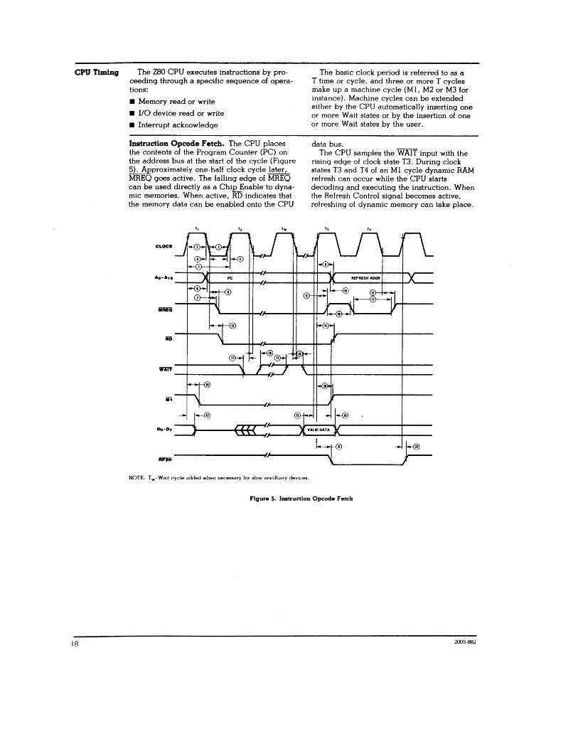
CPU Timing The Z80 CPU executes instructions by pro- The basic clock period is referred to as a
18
ceeding through a specific sequence of operations:
• Memory read or write
• I/O device read or write
• Interrupt acknowledge
Instruction Opcode Fetch. The CPU places the contents of the Program Counter (PC) on the address bus at the start of the cycle (Figure 5). Approximately one-half clock cycle later, MREQ goes active. The falling edge of MREQ can be used directly as a ChiEJ:nable to dynamic memories. When active, RD indicates that the memory data can be enabled onto the CPU
T, T2 Tw
CLOCK
Ao-Au _ ...... _J
«( ( ~
T time or cycle. and three or more T cycles make up a machine cycle (Ml. M2 or M3 for instance). Machine cycles can be extended either by the CPU automatically inserting one or more Wait states or by the insertion of one or more Wait states by the user.
data bus. The CPU samples the WAIT input with the
rising edge of clock state T3. During clock states T3 and T4 of an Ml cycle dynamic RAM refresh can occur while the CPU starts decoding and executing the instruction. When the Refresh Control signal becomes active, refreshing of dynamic memory can take place.
__ --.--,r" ______ I.-f'! f--® RFSH ~ _______ J~
NOTE: Tw- Wait cycle added when necessary lor slow ancilliary devices.
Figure 5. Instruction Opcode Fetch
2005·882

CPU Timing (Continued)
2()()~ 881
Memory Read or Write Cycles. Figure 6 shows the timing of memory read or write cycles other than an opcode fetGh (Ml) cycle. The MREQ and RD signals function exactly as in the fetch cycle. In a memory write cycle, MREQ also becomes active when the address
T,
CLOCK
{
iiii
0 ... 0'=: Do-D7
o ... .:::!:
Tw
;'
bus is stable, so that it can be used directly as a Chip Enable for dynamic memories. The WR line is active when the data bus is stable, so that it can be used directly as an RlW pulse to most semiconductor memories.
{
WR
Do-D7----__________ ~--------~~--~D~A~TA~O~U~T------------~
Figure 6. Memory Read or Write Cycl ..
19

CPU Timing (Continued)
20 .
Input or Output Cycles. Figure 7 shows the timing for an 110 read or 110 write operation. During 110 operations, the CPU automatically
Tw'
CLOCK
Ao-A
Wiii
inserts a single Wait state (Tw). This extra Wait state allows sufficient time for an I/O port to decode the address and the port address lines.
Tw
--r-~---+--------~~~~'
{
WR
WRI~: OPERATION ------i..--------..,)'----~;;;;~--~ Do-D7
NOTE: Tw" = One Wait cycle automatically inserted by CPU.
Figure 7. Input or Output Cycles
Interrupt Request/Acknowledge Cycle. The CPU samples the interrupt signal with the rising edge of the last clock cycle at the end of any instruction (Figure 8). When an interrupt is accepted, a special Ml cycle is generated.
During this Ml cycle, 10RQ becomes active (instead of MREQ) to indicate that the int'3rrupUng device can place an 8-hit vector on the data hus. The CPU automatically adds two Wait states to this cycle.
AO-A15 _________ ~-'.~---------p-C--~----+r~~--~-~--,~---
Wiii __________ ~-----------------~--~~J - r@ Do-D7====:t~-------~~=;;::JS~K:
NOTE: 1) TL = Last state of previous instruction. 2) Two Wait cycles automatically inserted by CPU(").
Figure 8. Interrupt Request/Acknowledge Cycle
2005·884. 885
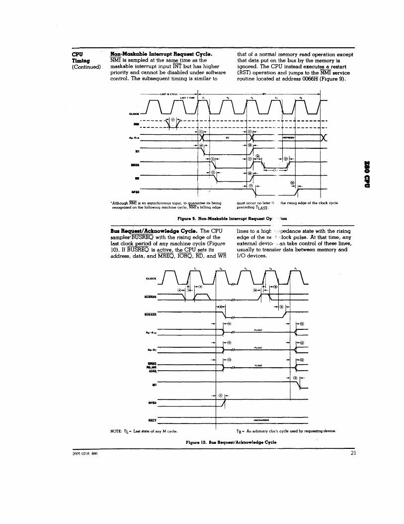
CPU Timing (Continued)
20050218. 886
Non-Maskable Interrupt Request Cycle. NMI is sampled at the same time as the maskable interrupt input INT but has higher priority and cannot be disabled under software control. The subsequent timing is similar to
CLOCK
... -....
that of a normal memory read operation except that data put on the bus by the memory is ignored. The CPU instead executes a restart (RST) operation and jumps to the NMI service routine located at address 0066H (Figure 9).
____________________ +-"~~----------_+J~-------
• Although NMI is an asynchronous input. to ~antee its being recognized on the following machine cycle. NMl's falling edge
must occur no later H the rising edge of the clock cycle preceding TLAST.
Figure 9. Non-Maskablelnterrupt Request Op' 'lon
Bus Request/Acknowledge Cycle. The CPU samples;:BUSREQ with the rising edge of the last clock period of any machine cycle (Figure 10). If BUSREQ is active, the CPU sets its address, data, and MREQ, 10RQ, RD, and WR
lines to a higr, ,. '1 pedance state with the rising edge of the nE !. :lock pulse. At that time, any external devic!' ,an take control of these lines, usually to transfer data between memory and I/O devices.
" T,
CLOCK
SUSNEQ ----------~~--~_+----7~--------J
T, 1,
... -.... ==========tj----.,(~-----~~--------t1 h-D1::::::::::::::::::::t=~---.,(~------~~--------t-4
~--------------------+-~ ~.--------~r"",1--------11
111
@--
IiALT UNCHANGED
--------------------+--------------------------------NOTE: TL = Last state of any M cycle. TX = An arbitrary clock cycle used by requestinQ device.
Figure 10. Bus Requestl Acknowledge Cycle
21
I 9

CPU Timing (Continued)
22
BaIt Acknowledge Cycle. When the CPU receives a HALT instruction, it executes NOP states until either an INT or NMI input is
received. When in the Halt state, the HALT output is active and remains so until an interrupt is processed (Figure 11).
.1 _I_ .1 -I- .1 ~ ~ ~ ~ ~ ~ ~
CLOCK
• • HALT
::::;-I0Il ~_. ___________ _ .. M. ~
NOTE: INT will also force a Halt exit. "See note, Figure 9.
Figure 11. Halt Acknowledge Cycle
Reset Cycle. RESET must be active for at least three clock cycles for the CPU to properly accept it. As long as RESET remains active, the address and data buses float, and the control outputs are inactive. Once RESET goes
CLOCK
Ao-A15
Do-D7
iiIl ___________ .Jf I
inactive, two internal T cycles are consumed before the CPU resumes normal processing operation. RESET clears the PC register, so the first opcode fetch will be to location 0000 (Figure 12).
_M1------
~R~
R~----------~7~7~7~---~;~J~----------------------~\~---------------==: III/III ~ ________ _ BUSACK
HALT
Figure 12. Reset Cycle
2005·887, 888
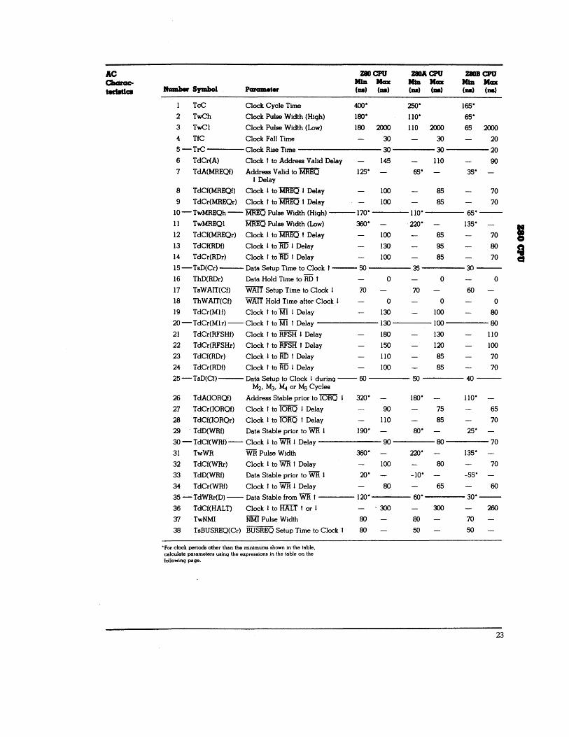
AC ZIG CPU ZIOACPU ZIG. CPU QuIrac- MID Max Mba Max MID Max terlatlCli IfUlDha- Symbol PCll'CllDeter ( .. ) ( .. ) (ill) ( .. ) ( .. ) ( .. )
TcC Clock Cycle Time 400* 250* 165*
2 TwCh Clock Pulse Width (High) 180* 110* 65*
3 TwCl Clock Pulse Width (Low) 180 2000 110 2000 65 2000
4 TfC Clock Fall Time 30 30 20 5-TrC Clock Rise Time 30 30 20
6 TdCr(A) Clock , to Address Valid Delay 145 110 90
7 TdA(MREQf) Address Valid to MREQ 125* 65* 35* I Delay
8 TdCf(MREQf) Clock I to MREQ I Delay 100 85 70
9 TdCr(MREQr) Clock , to MREQ , Delay 100 85 70
10 - TwMREQh -- MREQ Pulse Width (High) ---170* 110* 65*--
11 TwMREQI MREQ Pulse Width (Low) 360* 220* 135*
I 12 TdCf(MREQr) Clock I to MREQ , Delay 100 85 70
13 TdCf(RDf) Clock I to RD I Delay 130 95 80 I 14 TdCr(RDr) Clock , to RD I Delay 100 85 70
15 - TsD(Cr) --- Data Setup Time to Clock' --- 50 35 30--
16 ThD(RDr) Data Hold Time to RD , 0 0 0
17 TsWAIT(Cf) WAIT Setup Time to Clock I 70 70 60
18 ThWAIT(Cf) WAIT Hold Time after Clock I 0 0 0
19 TdCr(Mlf) Clock , to Ml I Delay 130 100 80
2O-TdCr(Mlr)-- Clock' to Ml I Delay 130 100 80
21 TdCr(RFSHf) Clock , to RFSH I Delay 180 130 110
22 TdCr(RFSHr) Clock I to RFSH , Delay 150 120 100
23 TdCf(RDr) Clock I to RD I Delay 110 85 70
24 TdCr(RDf) Clock , to RD I Delay 100 85 70
25 - TsD(Cf) --- Data Setup to Clock I during -- 60 50 40--M2, M3, ~ or Ms Cycles
26 TdA(lORQf) Address Stable prior to IORQ I 320* lSO* 110*
27 T dCr(lORQf) Clock , to IORQ I Delay 90 75 65
28 TdCf(lORQr) Clock I to IORQ , Delay 110 85 70
29 . TdD(WRf) Data Stable prior to WR I 190* SO* 25*
30 - TdCf(WRf) -- Clock I to WR I Delay 90 80 70
31 TwWR WR Pulse Width 360* 220* 135*
32 TdCf(WRr) Clock I to WR I Delay 100 80 70
33 TdD(WRf) Data Stable prior to WR I 20* -10* -55*
34 TdCr(WRf) Clock , to WR I Delay 80 65 60
35 -TdWRr(D)-- Data Stable from WR , 120* 60* 30*--
36 TdCf(HALT) Clock I to HALT t or I . 300 300 260
37 TwNMI NMI Pulse Width 80 SO 70
38 TsBUSREQ(Cr) BUSREQ Setup Time to Clock , 80 50 50
"For clock periods other than the minimums shown in the table, calculate parameters using the expressions in the table on the follOWing page.
23

AC Charac-terlstics (Continued)
24
zeD CPU Min Max
Number Symbol Parameter (us) (us)
39 ThBUSREQ(Cr) BUSREQ Hold Time after Clock 1 a 40 -TdCr(BUSACKf)-Clock 1 to BUSACK 1 Delay 120 41 TdCf(BUSACKr) Clock 1 to BUSACK 1 Delay 110 42 TdCr(Dz) Clock 1 to Data Float Delay 90 43 TdCr(CTz) Clock 1 to Control Ou!puts Float 110
DelaY.J!AREQ. IORO. RD. and WR)
44 TdCr(Az) Clock 1 to Address Float Delay 110 45 - TdCTr(A) ---Address Stable after MREQ 1.-- 160"
IORO I. RD I. and WR 1 46 TsRESET(Cr) RESET to Clock 1 Setup Time
47 ThRESET(Cr) RESET to Clock 1 Hold Time
48 TsINTf(Cr) INT to Clock 1 Setup Time
49 ThINTr(Cr) INT to Clock 1 Hold Time
50 - TdMlf(IORQf) - Ml 1 to IORQ 1 Delay
51 TdCf(IORQf) Clock 1 to lORQ 1 Delay
52 TdC£(IORQr) Clock 1 to IORQ 1 Delay
53 TdCf(D) Clock 1 to Data Valid Delay
"For clock periods other than the minimums shown in the table, calculate parameters using the following expressions. Calculated values above assumed TrC = TIC = 20 ns.
Footnotes to AC Characteristics
90 a
80 a
920"
110 100 230
Z80ACPU Min Max (us) (us)
a 100 100 90 80
90 80"
60 a
80 a
565" 85 85
150
Number Symbol Z80 zeOA zeOB
Z80B CPU Min Max (us) (us)
a 90
90
80
70
80 35"--
60 a
70 a
365"--70 70
130
TcC TwCh + TwCI + TrC + TIC TwCh + TwCI + TrC + TIC TwCh + TwCI, + TrC + TIC
2 TwCh Although static by design, Although static by design. Although static by design, TwCh 01 greater than 200 /LS TwCh 01 greater than 200 JLS TwCh 01 greater than 200 JLS
is not guaranteed is not guaranteed is not guaranteed
7 - TdA(MREQI) - TwCh + TIC - 75 ---- TwCh + TIC - 65 ---- TwCh + TIC - 50 ----
to TwMREQh TwCh + TIC - 30 TwCh + TIC - 20 TwCh + TIC - 20
II
26
TwMREQI
TdA(IORQI)
TcC - 40
TcC - 80
TcC - 30 TcC - 30
TcC - 70 TcC - 55
29 TdD(WRf) TcC - 210 TcC - 170 TcC - 140
31-TwWR---TcC - 40-------TcC - 30 TcC - 30-------
33 TdD(WRI) TwCI + TrC - 180 TwCI + TrC - 140 TwCI + TrC - 140
35 TdWRr(D) TwCI + TrC - 80 TwCI + TrC - 70 TwCl + TrC - 55
45
50
TdCTr(A) TwCI + TrC - 40
TdMlf(lORQI) 2TcC + TwCh + TIC - 80
AC Test Conditions: VIH = 2.0 V VIL = 0.8 V VIHC = VCC -0.6 V VILC = 0.45 V
VOH = 2.0 V VOL = 0.8 V FLOAT = ±0.5 V
TwCI + TrC - 50 TwCI + TrC - 50
2TcC + TwCh + TIC - 65 2TcC + TwCh + TIC - 50

APPENDIX F •••• FLOPPY ERROR CODE
36
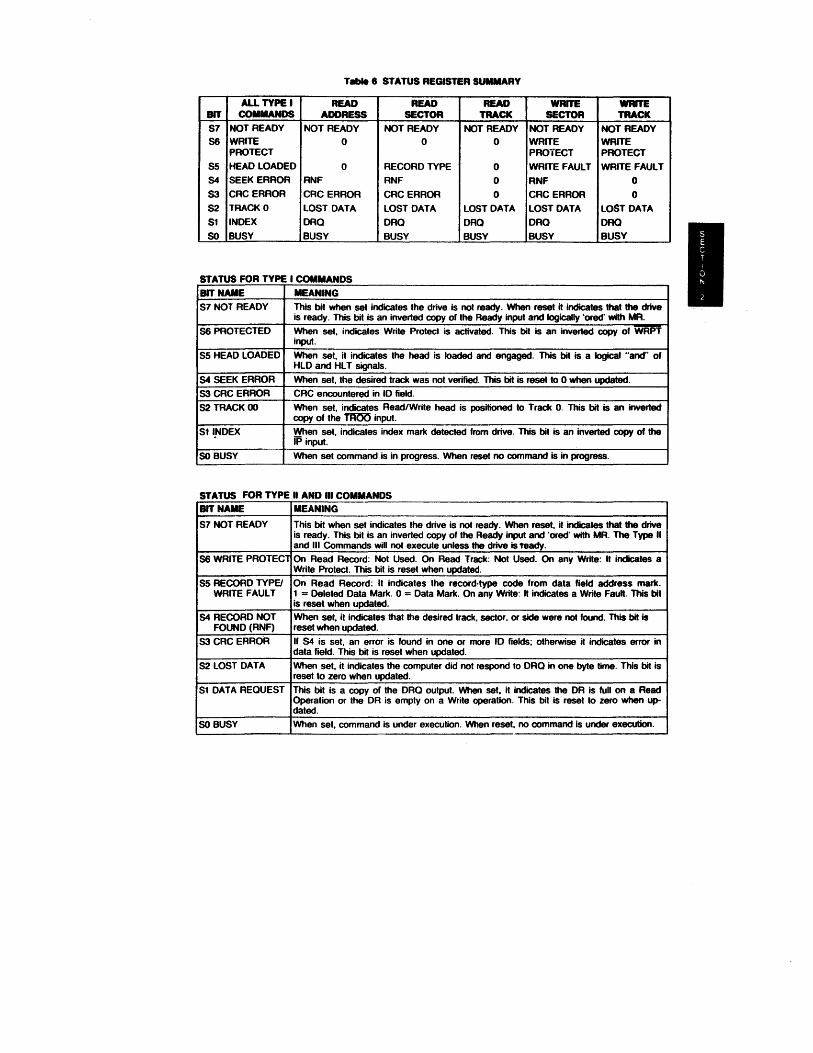
Table 8 STATUS REGISTER SUMMARY
ALL TYPE I READ READ READ WRITE WAITE BIT COMMANDS ADDRESS SECTOR TRACK SECTOR TRACK
S7 NOT READY NOT READY NOT READY NOT READY NOT READY NOT READY
S6 WRITE 0 0 0 WRITE WRITE PROTECT PRO-iECT PROTECT
S5 HEAD LOADED 0 RECORD TYPE 0 WRITE FAULT WRITE FAULT
S4 SEEK ERROR RNF RNF 0 RNF 0
S3 CRC ERROR CRC ERROR CRC ERROR 0 CRC ERROR 0
S2 TRACK 0 LOST DATA LOST DATA LOST DATA LOST DATA LOST DATA
S1 INDEX ORO ORO ORO ORO ORO
SO BUSY BUSY BUSY BUSY BUSY BUSY
STATUS FOR TYPE I COMIIANDS
BIT NAME MEANING
S7 NOT READY This bit when .set indicates the drive is not ready. When reset it indicates that the drive is ready. This bit is an inverted copy of the Ready input and logically 'orad' with MR.
S6 PROTECTED When set, indicates Write Protect is activated. This bit is an inverted copy of WRP'f input.
S5 HEAD LOADED When set, it indicates the head is loaded and engaged. This bit is a logical "and" of HLD and HL T signals.
S4 SEEK ERROR When set, the desired track was not verified. This bit is reset to 0 when updated.
S3 CRC ERROR CRe encountered in 10 field.
S2 TRACK 00 When set, indicates Read/Write head is positioned to Track O. This bit is an inverted copy of the moo input.
S11.NDEX ~n set, indicates index mark detected from drive. This bit is an inverted copy of the IP input.
so BUSY When set command is in progress. When reset no command is in progress.
STATUS FOR TYPE II AND III COMMANDS
BIT NAME MEANING
S7 NOT READY This bit when set indicates the drive is not ready. When reset, it indicates that the drive is ready. This bit is an inverted copy of the Ready input and 'ored' with MR. The Type II and III Commands will not execute unless the drive is teady.
S6 WRITE PROTECT On Read Record: Not Used. On Read Track: Not Used. On any Write: It indicates a Write Protect. This bit is reset when updated.
S5 RECORD TYPEJ On Read Record: It indicates the record-type code from data field address mark. WRITE FAULT 1 = Deleted Data Mark. 0 = Data Mark. On any Write: It indicates a Write Fault. This bit
is reset when updated.
S4 RECORD NOT When set, it indicates that the desired track, sector, or side were not found. This bit is FOUND (RNF) reset when updated.
S3CRC ERROR If S4 is set, an error is found in one or more 10 fields; otherwise it indicates error in data field. This bit is reset when updated.
S2 LOST DATA When set, it indicates the computer did not respond to ORO in one byte time. This bit is reset to zero when updated.
S1 DATA REOUEST This bit is a copy of the ORO output. When set, it indicates the DR is full on a Read Operation or the DR is empty on a Write operation. This bit is reset to zero when up-dated.
SO BUSY When set, command is under execution. When reset, no command is under execution.

FD171XA-G2 ~ PACKAGE FD171XIJ.02 PLASTIC PACKAGE
ThIs Is • pnIIimNry spec:iIIcation wlIh tentative device parameters ... INV be IUIIjed to change ... IInII procb:t cNI .... luIoI. Is CCIfIIIIIeIed· IrIIorIMIIOn ......... ~ WeIIem DigIIIII CorponIIIon Is believed to be .ccurIiIIt InCf ....... ~, no ,......, Is ....... ~ w..m DigIIIII CorpcnIIon for ill use; nor .., iillingll"'lInlS aI peIIInIS or 08ier rIghIS all*d ~ wIik:h INV ................ No ..... Is granIIId.~ IrnpIicIIIIon or 0IherwiIe under .., peIenI or paIIInI rigIiIS 01 WeItem DigIIIII CorponiIIon. WeIIem DigIIIII CoIpoqIon .....".. .. right to change Uid drcuMry .. ..,.".. wIIiouI noIIcII.
W,.T'1I111 DllllrAI. CD. , D • A , , D M
3128 REDHILL AVENUE, BOX 2180 NEWPORT BEACH, CA 92863 (714) 557-3550,TWX 910-585-1138
354

TECHNICAL APPLICATION NOTES FOR THE SUPER QUAD SINGLE BOARD COMPUTER.
In case of problems with the SUPER QUAD: these are two thing a customer may do: 1. send the product back for warranty service(turn around time is 1 day) 2. follow thw following notes and then if there are still no results do
the first stepl
1. If the board is totaly dead and won't communicate with the CRT, then do the following: a. check you power supply for 5,+,-12 volts. b. check pins 1,3,17 of the U53(BR1941) baud rate gen. for step type
pulses.(if you do not see any thing on these- pins then replace the BR194l chip)
I I I I I I
c. Check your PS NET/I the serial port adapter cable for possible loss of + or - 12 volts or the 1488 chip.
d. check pin 3 of U11(74ls11). there should be a positive going signal{about 5 volts) and when you press RESET you should see that pulse going to ZERO voltage.
e. If the step d is OK then you have a problem with either on of the a or b or c •
f. ~heck the 4MHZ clock signal 90in9 to pin 6 of the CPU.
2. If there is a problem with the floppy disk controller part only and you think that the phase lock loop needs to be adjusted, then follow the folowing steps:
a. This is done with the help of a dual trace scope. b. put one channel on the 4MHZ signallPIN 6 of the cpu chip)
put the other channel on pin 7 of the U27(74sl24) and by tweeking the R26(pot) those two signals are supposed to lock.
c. the above procedure is only recomended to engineeres or techriicians with experience of doing such things before.
3. Make SUle the board is being properly cooled by a fan.
4. The power consumption of the board is: +8v--- 1.8 amps max. +16---.4 amps max. -16--- .2 amps max.
5. To ensure the proper operation of your floppy disk drives, make sure to put the termination resistor at the end of the cable.
6. Reter to the softare manual for software problems.
38

Application notes to run TURBO-DOS operating system:
If you have one of the early revisions of the SUPERQUAD check the following:
1. pin 13 of the eTC should be hooked to +5V.
2. R17 should be hooked to +5.
3. for double sided drives, there should be a jumper from j3 connector to PlO bit3(PIO-29)
4. IE3 1in2 (PIO-22) should goto uI8-9, on some older tev. boards its also going to pin 12 of u14. the place to cut would be on top of uS right above pin 20 there is a pad hole; the etch going north should be cut, then install a jumper from ul4-12 to ul5-6
39

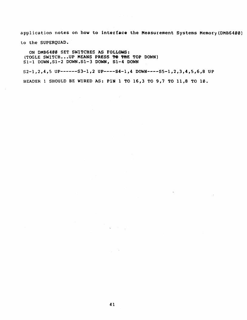
application notes on how to interface the Measurement Systems Memory (DMB6400)
to the SUPERQUAD.
ON DMB6400 SET SWITCHES AS FOLLOWS: (TOGLE SWITCH ••• UP MEANS PRESS 'K) ME TO·P DOWN) 51-1 DOWN,Sl-2 DOWN.Sl-3 DOWN, Sl-4 DOWN
52-1,2,4,5 UP------S3-l,2 UP----$4-1,4 DOWN----S5-1,2,3,4,5,6,8 UP
HEADER 1 SHOULD BE WIRED AS: PIN ITO 16,3 TO 9,7 TO 11,8 TO 10.
41
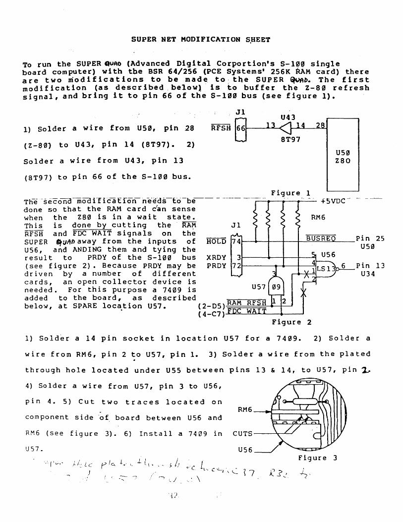
SUPER NET MODIFICATION ~HEET
To run the SUPER aUAt) (Advanced Digl tal Corportion's S-10B single board computer) with tbe BSR 64/256 (PCE Systems' 256K RAM card) there are two ni 0 d 1 f i cat Ion s to be mad ~. to: the SUP E R GluAb. The fir s t modification (as described. below) Is to buffer the Z-80 refresh signal, and bring it to pin 66 of the 5-109 bus (see figure 1).
1) Solder a wire from US0, pin 28
(Z-S0) to U43, pin 14 (8T97). 2) US0
Solder a wire from U43, pin 13 zeo
(BT97) to pin 66 of the 5-1"" bus.
Figure 1 Th-e -s'ec'ona-mooi-fi'catfon-ne-eas-to-be-- - ----- --~-----.--...--~-- +5VDCdone so that the RAM card c~n sense when the ze" is in a wait state. This is done by cutting the RA~ Jl
RM6
RFSH and FDC WAIT signals on the SUPER "tVAI> away from the inputs of HOLD ~-+ __ r--+ __ ~~B~U~S~R~E~ ___ Pin 25
US6, and ANDING them and tying the result to PRDY of the 5-1"" bus XRDY (see figure 2). Because PRDY may be PRDY driven by a number of different cards, an open collector device is needed. For this purpose a 7409 is added to the board, as described below, at SPARE location US7. (2_DS)~R~A~M~~~~~_
• (4-C7)~~C~~~~----Figure 2
usa
Pin 13 )~-
U34
1) Solder a 14 pin socket in location US7 for a 7409. 2) Solder a
wire from RM6, pin 2 to US7, pin 1. 3) Solder a wire from the plated
through hole located under U5S between pins 13 & 14, to US7, pin 1.
4) So 1 d era wi ref rom U 5 7, pin 3 to U 56,
pin 4. 5) Cut two traces located on .
component side 'of, board between U56 and
RM6 (see figure 3). 6) Install a 7409 in
US7.
',', f) C,- )./~ L c
" ! I _
. /, > I
" :~ J
RM6
CUT S ---'r-~
U56 Figure 3 , ~-

12.0 Parts list
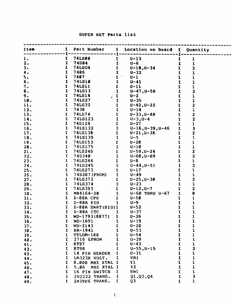
SUPER NET parts 1 ist
~~-~------------------------------------------------------~---------------Item I Part Number I Location on board I Quantity ---------------1-----------------1---------------------I-------------~~---1. I 74LS88 I U-ll I 1 2. I 74S94 I U-6 I 1 3. I 74LS04 I U-1S,U-34 I 2 4. I 7406 I U-32 I 1 ~. I 7497 I U-l I 1 6. I 74LS18 I U-41 I 1 7 • I 74LSll I U-ll I 1 8. I 74LS13 I U-47,U-56 I 2 9. I 74LS14 I U-2 I 1 1". I 74LS27 I U-35 I 1 11. I 74LS32 I U-42,U-22 I 2 12. I 7438 I U-14 I 1 13. I 74LS74 I U-33,U-40 I 2 14. I 74LS123 I lJ-3,U-4 I 2 15. I 745124 I U-27 1 1 16. I 74L5132 I U-16,U-39,U-46 1 3 17. I 74LS138 I U-21,U-36 . I 2 18. I 74LS139 I U-5 I 1 19. I 74LS153 I U-28 1 1 20 • I 74L517S I U-10 I 1 21. I 74L5240 I U-S9,U-24 I 2 22. t 745240 I U-68,U-69 I 2 23. I 74LS244 I U-8 1 1 24. I 74LS245 I U-44,U-S1 I 2 25. I 74LS273 I U-17 I 1 26. I 745287 (PROM) 1 U-49 I 1 27. I 74LS373 I U-2S,U-30 I 2 28. I 74L5374 I U-23 I 1 29. I 74LS393 I U-12,U-7 I 2 30. I MB4164-21 1 U-60 THRU u-67 I 8 31. I Z-8QA CPU I U-S0 I 1 32. I Z-80A PIa I U-9 1 1 33. I Z-80A DARTlSIO)I U-S2 I 1 34. I Z-80A eTC I U-37 I 1 35. I WD-1793(8877) 1 U-26 I 1 36. I WD-1691 I U-19 I 1 37 • I WD-2143 I U-20 I 1 38. I BR-1941 I U-S3 I 1 39. I TTLDM-100 I U-S4 I 1 4". I 2716 EPROM I U-29 I 1 41. I 8T97 I U-43 I 1 42. I 8T98 1 U-SS,U-lS 1 2 43. 1 14 PIN HEADER 1 U-31 1 1 44. I Lf4i323K VOLT. I VR1 1 1 45. I 8.00" MHZ XTAL I Yl 1 1 46. I 5.06 MHZ X'l'AL I Y2 I 1 47 • I 16 PIN SWITCH I SW1 I 1 48. 1 2N2222 TRANS. 1 01,Q2,04 I 3 49. I 2N3ge6 TRANS. I 03 I 1
1

50. I 78L12 I Q5 I 1 51. I 220 MH CHOKE I L1,L2 I 2 52. I 4.7K SIP I RM1,RMl,RM7 I 3 53. I 10K SIP I RM2,RM5 I 2 54. I 33 OHM SIP I RM6 I 1 55. I 220/330 SIP I RM4 I 1 56. I 33 OHM DIP I RMa I 1 57. I IN9l4 DIODE I CR2 I 1 58. I 5.1 V ZENER I CRl I 1 59. I 1"" MF CAP I C2 I 1 68. I .1 MF CAP I I 21 61. I 4.7 MF CAP I C6,Cl,Cll,C27,C281 8 62. I 10K POT I R27,R28 I 2 63. I 14 PIN HEADER I ·J4,J5 I 2 64. I 58 PIN HEADER I J3 I 1 65. I 40 PIN HEADER I J2 I 1

13.e Schematic diagram

o
c
B
A
8
(A-C ~) (1 - B'.> ) (2-O{,)I....;Rc..:..:D=--__ -t--=-I9
( ~ .u.,) (1.I)~)-::!W'±!VR:O::=::=-----11_'5=-t (t.es, IOREQ II
(~,Ob) (~-I\\ )...,,;M~R-'=E..:=Q--_:3::-t (Il-In) (>;D&)...:..M=I ____ 7-;
U'l3
8T,,}1
'L'5
7
1\0 4 IZ '20 2. 1")
6 27
U34 )( RDY j \--~_--t---t_-5"-i usc:, L 504
P R DY 12 i ~~12=e-+-,-~.q-'-l ~~ V
~
(2.-D5'1~ ( 4-( 7) fi5f"WAiT ( 2 -c.2) WAif
U50
e60
A0 '11 A1
A2
A4 ,., A? A0
~1 A7 A8
40 A10.
A12
" A14
14 D0 15 D1 '2. D2
DJ D4 05
to 13 D7
RISrt .f~-DB~ (4-. Bl)
6
Ai A'L
A4 At;
Al
"
.--t? 1'2.4
Uc.9
'271(0
~1! 1~~U5~: 8 A15 Il
UII '3
I L??NL--
(~-f'>2.) PROM EN -:.;/
(2~1)~BUS~A-CK---4----~E~U~S~~~(~K~------------------------------__,
PINT
YIC
Yrl
1 14
f.1S 1K
'-----4~--_----JV'o.l'A..,.....~- + E>
5
10
11
t3
14
If> t7
2.46B9753
I R.Mc..
10K.
+? Q+ ~ 1 K. (2.M, PD BIW. CD l' 7 RM1'
H-----t "-.-1 U49 ~ W
00
D2 V3 04 D?
D7
4
J\ r-
3
L ZON E.1 LTR I
I I I
" 22 AOtJB
01 V 02 V D3
D4 D'7
D7
13.
AI A2 17
4 A4 14 A5 8
18
Al
L '50'l -BJ\1 UI8 (2-<"1-)
U25
L5?7~
It. BAO L l~ BM/> lJ.. MIL eo It. BA'LL 51
1-15.--';;~=-:-:--'-t--i ,1 J-";:.5_BA+=--'-:1--1 ~ 1-9,,--Bt6_--"-ct--i 2 ~ 115 8"" / 52 .... ..2.=--::B"",A7"'--"----t53 BA7
...--+ _____ 1 .. 11 " 6P5TVAL(2_Cl) ,T 11
e
A5
Ali A12
AI4 Ai'=»
U23 L5~74
14 7.
IS
B 17
I~
U30 Leo ~l?
J1 r-
1-'2=------t---1 1(0 A \(0 I-~=-----t---i 17 ...,<D~---t---i 15 t-"'''-----t---i 59 1-1,....2 -----t--t" I 1-"",-5 ----;---1 (OZ 1-".::."----;---1 (o~ 1-,~~----;---1<D4 A'l3
III~
I"--.:D:...r......0_....c1'=-l2 1-'8"--__ -; 3tQ DO¢ I~D~1~~I~1 9 35 ~D=2 __ ~I~~ ? M
D3 14 U44 6 Sg I ~D'"""4----'-I..!.f ~ L 5245 5 3a
I~D~?_~1~1 4 ~ 1 '-7D-=41_--,-17-'-1 3 40 '-'0"-'7'------'1 ...... B ..2.. 90 007
.-----IZ3 DoD~oL..
+5 _-J\e/\~A"1'.I'"!.v-"'I/~J-_---'1 r--__ L.--______ --'
~ AO-AI5
LS04 MI U34
I 2.
I 11.0
'5
6
2
U3&
L5138
(.,-08) _~RD ___ ---'~1-'U_4_1""
d o L':>lO"'-~ .... 8 _____ 0=-j
Ull L5135
" I -
+BV
GND
+IG,V
-I" V 52. \------- -IGV
I QTY I CODE I REQD IDENT
UNLESS OTHERWISE SPECIFIED DIMENSIONS ARE IN INCHES TOLERANCES ARE:
3
PART OR 1 IDENnFYING NO.
CONTRACT NO
FRAcnONS DECIMALS ANGLES vv I ~ 11.17 12 8'-
(HZ. \. i'iR"5"MON 'I \0 ;,.
..11-96 15 +5
UIB L 504
21\12222 ('2.&z)(~.J;; RAMHJ !l PROM rl'-2.3 , J CIS (2-87 ) soUT JI-46 1 L J "'} ('--___ .:['~44-+ 1 . ..Ott~-iBi:.lO~A~Rl.l=D~....r.I;.:/:..:;O::...-_______________ ~.--______ -,
:t:: .XX :::'::: ::!:
.xxx +
MATERIAL
APPROVALS
DRAWN ASG DESIGN':! CHECKED
FINISH
3~) PRI-3
NEXT ASSY USED ON
APPLICATION DO NOT SCALE DRAWING
J9\ BISWOP GRAptUCS. INC '<81 REOROER NO. 2050S 8 7 6 5 4 3
2
15 5lC5IS 14 DIOC.~ ,:, Ef[c.c, 12 FOCCS
4
REVISIONS
DESCRIPTION
~-D5}
(3-(0)
(~-03)
(4-ce)
NOMENCLATURE OR DESCRIPTION
PARTS LIST
1
SUPER QUAD 5-100 BOf\RD DATE
11-/9-81
2
ADVANCED DIGITAL COR?
SCHEMATIC
So I CODE IDENT NO IDRAWING NO.
1
APPROVED
o
c
B
A
A

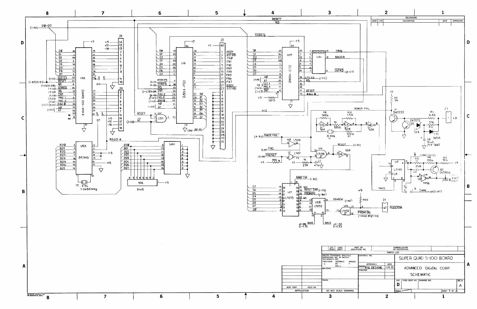
o
c
B
A
8 7 6 5
c1_~~ __ ~oa~-_O~7~ ______ ~ ____________________________ -+~ ____ ~ ________________________________________ ~
~ ~
D~ 40
DI I
D2 ~ D3 2. D4 ~
05 3
07 4
('-C2) ~SI~D!:;::C=':S;L-----=-3'j=-t (1- B7) (+-B 7·~ _____ R,-"E~S=E...:..T_-=2.1'-t
(~·CG>}f'-D8) ~=r; 8 (;,-CCD' .l.uRt:l>I J~
("'_CcOl---:"Jffi~ __ -,,-3,2
(;-c"" INT 0;
(">;.C~) PRI-I 6 ('3-ffi) PRt-~ 7
(1.[1) t~-Cb) 'lBO di to A0 H
&01 '; BD2.. tJ
BO? 7
807
IB\ BISHOP GRAPHICS, INC. 'til' REORDER NO. 20505 8
U52-
'P II:
8 o H U1
J
ti III
hJ
J5 -+0;-14 +1'l-12 -1.0- "
~\~~-----------_1 2 .....,1tCL..... ____ --I ~ .....,'."'-2. _______ ---1 4 !-'-1b=-_______ -i OJ
.....,1=~ _________ ---I~
~'...:..1---------t 7 ~1~b--------tB 14
~ 06 ___ -I~
40---10 '-
~ ~2~?----_1----~6 ~'l:=.z--___f--~ 2 r1~~--_1--~ , 1-"2.::o.e, __ _1---~ 4 1-'-2~~ ___ ~ ___ -;~ p:Z=~ ____ ~ __ -; (0
..,,2-'...4 --=---=-_1--~ 7 ~~ ~u--t----i '?
~?-14
~'2 - 1"2 -10-13
10 -Br-.UD A
D0 01 20 02 D3 4-0
04 05
07 1
(I-ezl 'PWC5 4 (~.{e) IOREQ ~
RD 35
'2. UII
(3-DB Mf
I 1300 9 5WI
r~~Djl~-------------'~C
BD2 II BV3 llo e>D4- 13
5D'" 14 / &D0 15
501 16
987654~J I 101(
RM5
7 6
U9
8 a...
J2 ...........
t? -40
... '=5 _____ -; 1 ARDY
... '..:..." _____ -; 3 rnRB
...,'~'i _____ ---1 ') PM/)
... ,..-'--------i 7 PAl rf=-3 --------1 <) PAl ~f1~-----------Ill PA' E'Q~-----,I~ PA4 ... ~~------i17 PA5 1-'-0~------i17 PA~ j-!1-------I19 PA7 1-='7.,,-1 -----------121 ~ 1-'-t1~-----_i23 B5TRB
21 Be! 28 61 19 B2 }() 53 31 54 "-32 B? ~~ 50 .34 B7
r-- 2 ~4
~" ~B ~Ill
~J2 ~14
~Ib
~15
~20
~22
.-- 24 ~10
~28
,.-- "0 ~'1.
5 i
4
D2 D? D4 D? 0& D7
2'7
11 U37
U I-
lJ I
<{
3
I (HEADER) 14-
12. U3\ 12.
21 q
20
ArJ IS
(1-111) [~A::,-::1 :-:-_--2'!..L'3-1 o (()
IIoCTC-!:S O-C2.) N Co lfE
+5 I1H-1 17 (3-(S) PRl-1 It
(I-c.-7I niT 11
~J AA t5 51P-5
MI
(4 -IB) POWER FAIL
L~~4 ('L-B'll p.oe.. ~ utE:,
:; UI L707 L,) 131
If R6
t7 __ -'\A.A.fU-_~J ~ 21K 4.71LV
D7 18 01 c y
~.::::.D(O=--________ ---,-17':;D UI1 05 14 D
Q12 N~/C;;:....; ....... ~ G 16 RE5E.T IMP(j-csj
I MI-I~
BAUOA
POWEI'\ FAIL
I ~--;.g",,;'---------"I~"'-Ig L '3113 Q 15 PROMfN \'-I(Q ") Q~K ) G 9 1:3 'i 9 RAMEIJ '-A~) » RM.3
2 REVISIONS
I ZONE I LTR I DESCRIPTION
I I I
I t5
~ R5 <, 31\
I
JI D2 7 D Df :3 D D~ ~ D
6 12 U2.8 '-
~ is II L ?1 '53 .,...-U_lo..,..,I-='-3_.....,3<L-___ ---I ftJ 1 ?I-lA mo Nl G 2 10 pl.=!.5 __ !..CII Q L '?i3'2
&.:T-A _:;;e,~ JJ 12. PROM O~ 14 2 ~~~~~(~\-~A~~)~(I~-~~X~I-C~
.,11-86 BAI4-\.1-C.'3)
BAIS JI-32 (I-C3)
PART OR IDENTIFYING NO
UNLESS OTHERWISE SPECIFIED CONTRACT NO.
NOMENCLATURE OR DESCRIPTION
PARTS LIST
1
I OATE I APPROVEO
I I
SUPER QUAD 5-100 BOARD DIMENSIONS ARE IN INCHES TOLERANCES ARE:
NEXT ASSY USED ON
APPLICATION
4
FRACTIONS DECIMALS ANGLES
MATERIAL
FINISH
.XX ±
.xxx ±.
DO NOT SCALE DRAWING
3
APPROVALS DATE
ADVANCED DIGITAL CORP. ORAWNASG DESIGNS 11-19-81 CHECKED
SCHEMATIC
REV
A
2 1
o
c
B
A

7 • I
Pi
T.lO 61-_______ ri; P2
~--------=-...----ie; ")to ----l5-_________ --iC: ms 75188 _---..... )8 ill
om 8 L-----+-----fr-§~~,.~188--·---+------4\C DSR
__ --------_____ ~t~D~S~~ ___ ~CD mR en 5 em ~;.....;;;..--......
1
~ AD 4 8k.l0
'.,.1. - t -. ,,"'0 9 ~---;h "'0 ,,[R ·~ND 10 "!-
·',voe 12 ·----=-S+.h vDC -1~vDC 13L--.+-----<-16vDC +, voe 14L--.+--,...-t-<
-11..
7
lRX
- .. _- ---.. ---~
b8.:2.SS
6
20
"It. ~Afll' .. .aD 1
At) pow t'" C. ... D ,
.+ 4
t:NG. rl/A
_. LQ.~ I~ 121
P 5 QII..AD/1 /lDr/d1'(ED _
t I '. oJ
.~-
5 t--~A---~_-t ~t)' 2-7 1------1 74 L S t-. ------- J q 244 - .. 1/ II -.------ S-Q -~ IS" ? 11 8
" 9
i ;t,('! 8
1~ I . 2
:11 ~-.. -_··_--t '3, l--~ --=-----1
33 ~-------tt, 7 t-·--"-----t " .. 't-' ----t ~ PJ:jS
I I
. .
74LS 2 Lf 0 t-----------
PSq'tQtlJ>/ PA R 3- 2. 5- 92.
; j
I I
I LJ
l)/(' b 8 - 25 01\1
REV-C. ~~A~

NOTICE
Advanced Digital Corporation rON requires a Return Authorization Number for the return of any equipnent for repair or credit. This nurrber will be issued by the CUstater Support Departnent. Arr:l equipnent received without the Return Authorization Nuniber clearly marked on the outside of the package may be subject to significant delays in the repair process.
Return Authorization Numbers are active for 30 days after they are issued. If the equipnent specified in the Return Authorization is oot received by Advanced Digital within this 30 day period significant delays in handling the repair may be incurred.
If the equipnent must be returned a second time, a new Return Authorization Number must be issued. Reuse of Return Authorization Numbers may result in delays in processing returns.
Effective Novanber 1, 1981, repair of all kit and nonwarranty boards will be $70.00. This fee is subject to change without notice.
Returns for credit will be subject to a 15% restocking charge. If material for credit was purchased through a dealer, Advanced Digital cannot issue a credit. Adjust:m:mt must be handled through the dealer. Other credit returns should have reference to the original invoice number.
If you have any questions regarding special handling, packaging of the equipnent, or procedures for returning equipnent, please contact the Advanced Digital Corporation.
The warranty on the super quad is one year fran the date of purchase.