Technical Information Manual S78H-5142-00 PC 100...
58
IBM Technical Information Manual PC 100 (Type 6260) and PC 300 (Type 6560) S78H-5142-00
Transcript of Technical Information Manual S78H-5142-00 PC 100...

IBM
Technical Information Manual PC 100 (Type 6260) and PC 300 (Type 6560)
S78H-5142-00


IBM Technical Information Manual PC 100 (Type 6260) and PC 300 (Type 6560)
S78H-5142-00

Note
Before using this information and the product it supports, be sure to read the general information underAppendix B, “Notices and Trademarks” on page 43.
First Edition (August 1996)
The following paragraph does not apply to the United Kingdom or any country where such provisions are inconsistent withlocal law: INTERNATIONAL BUSINESS MACHINES CORPORATION PROVIDES THIS PUBLICATION “AS IS” WITHOUTWARRANTY OF ANY KIND, EITHER EXPRESS OR IMPLIED, INCLUDING, BUT NOT LIMITED TO, THE IMPLIED WARRANTIESOF MERCHANTABILITY OR FITNESS FOR A PARTICULAR PURPOSE. Some states do not allow disclaimer of express or impliedwarranties in certain transactions, therefore, this statement may not apply to you.
This publication could include technical inaccuracies or typographical errors. Changes are periodically made to the informationherein; these changes will be incorporated in new editions of the publication. IBM may make improvements and/or changes in theproduct(s) and/or the program(s) described in this publication at any time.
It is possible that this publication may contain reference to, or information about, IBM products (machines and programs),programming, or services that are not announced in your country. Such references or information must not be construed to meanthat IBM intends to announce such IBM products, programming, or services in your country.
Requests for technical information about IBM products should be made to your IBM reseller or IBM marketing representative.
Copyright International Business Machines Corporation August 1996. All rights reserved.Note to U.S. Government Users — Documentation related to restricted rights — Use, duplication or disclosure is subject torestrictions set forth in GSA ADP Schedule Contract with IBM Corp.
Contents
Preface . . . . . . . . . . . . . . . . . . . . . . . . . . . . . . . . . . . . . . . . . . . . . . . . . . . . . . . vRelated Publications . . . . . . . . . . . . . . . . . . . . . . . . . . . . . . . . . . . . . . . . . . . . . . . . vManual Style . . . . . . . . . . . . . . . . . . . . . . . . . . . . . . . . . . . . . . . . . . . . . . . . . . . . v
Chapter 1. System Description . . . . . . . . . . . . . . . . . . . . . . . . . . . . . . . . . . . . . . . . 1Personal Computer Description . . . . . . . . . . . . . . . . . . . . . . . . . . . . . . . . . . . . . . . . . . 2System Overview . . . . . . . . . . . . . . . . . . . . . . . . . . . . . . . . . . . . . . . . . . . . . . . . . . 3System Features . . . . . . . . . . . . . . . . . . . . . . . . . . . . . . . . . . . . . . . . . . . . . . . . . . 4System Board . . . . . . . . . . . . . . . . . . . . . . . . . . . . . . . . . . . . . . . . . . . . . . . . . . . . 6System Address Maps . . . . . . . . . . . . . . . . . . . . . . . . . . . . . . . . . . . . . . . . . . . . . . . 7
Memory Map . . . . . . . . . . . . . . . . . . . . . . . . . . . . . . . . . . . . . . . . . . . . . . . . . . . 7Input/Output Address Map . . . . . . . . . . . . . . . . . . . . . . . . . . . . . . . . . . . . . . . . . . . 7DMA I/O Address Map . . . . . . . . . . . . . . . . . . . . . . . . . . . . . . . . . . . . . . . . . . . . . 9
IRQ and DMA Channel Assignments . . . . . . . . . . . . . . . . . . . . . . . . . . . . . . . . . . . . . . 10Interrupt Request Assignments (IRQ) . . . . . . . . . . . . . . . . . . . . . . . . . . . . . . . . . . . . 10DMA Channel Assignments . . . . . . . . . . . . . . . . . . . . . . . . . . . . . . . . . . . . . . . . . . 10
Power Supply . . . . . . . . . . . . . . . . . . . . . . . . . . . . . . . . . . . . . . . . . . . . . . . . . . . . 11Power Output Parameters . . . . . . . . . . . . . . . . . . . . . . . . . . . . . . . . . . . . . . . . . . . . . 11
Component Outputs . . . . . . . . . . . . . . . . . . . . . . . . . . . . . . . . . . . . . . . . . . . . . . . 12Output Protection . . . . . . . . . . . . . . . . . . . . . . . . . . . . . . . . . . . . . . . . . . . . . . . . 12Connector Description . . . . . . . . . . . . . . . . . . . . . . . . . . . . . . . . . . . . . . . . . . . . . 13
Physical Specifications . . . . . . . . . . . . . . . . . . . . . . . . . . . . . . . . . . . . . . . . . . . . . . . 13Advanced Power Management (APM) . . . . . . . . . . . . . . . . . . . . . . . . . . . . . . . . . . . . . . 14
Chapter 2. Connectors and Jumpers . . . . . . . . . . . . . . . . . . . . . . . . . . . . . . . . . . . . . 15System Board Connectors . . . . . . . . . . . . . . . . . . . . . . . . . . . . . . . . . . . . . . . . . . . . 16
Diskette Drive Connector . . . . . . . . . . . . . . . . . . . . . . . . . . . . . . . . . . . . . . . . . . . . 16Hard Disk Drive Connectors (Primary/Secondary) . . . . . . . . . . . . . . . . . . . . . . . . . . . . . 17ISA Connectors . . . . . . . . . . . . . . . . . . . . . . . . . . . . . . . . . . . . . . . . . . . . . . . . . 18PCI Connectors . . . . . . . . . . . . . . . . . . . . . . . . . . . . . . . . . . . . . . . . . . . . . . . . . 19Power Supply Connectors . . . . . . . . . . . . . . . . . . . . . . . . . . . . . . . . . . . . . . . . . . . 20System Board Memory Connectors . . . . . . . . . . . . . . . . . . . . . . . . . . . . . . . . . . . . . . 21Video Feature Connector . . . . . . . . . . . . . . . . . . . . . . . . . . . . . . . . . . . . . . . . . . . . 22
I/O Connectors . . . . . . . . . . . . . . . . . . . . . . . . . . . . . . . . . . . . . . . . . . . . . . . . . . . 23Keyboard and Auxiliary-Device (Mouse) Connectors . . . . . . . . . . . . . . . . . . . . . . . . . . . . 23Serial Port Connectors . . . . . . . . . . . . . . . . . . . . . . . . . . . . . . . . . . . . . . . . . . . . . 24Parallel Port Connector . . . . . . . . . . . . . . . . . . . . . . . . . . . . . . . . . . . . . . . . . . . . . 25Monitor Connector . . . . . . . . . . . . . . . . . . . . . . . . . . . . . . . . . . . . . . . . . . . . . . . . 27
Chapter 3. Memory Subsystems . . . . . . . . . . . . . . . . . . . . . . . . . . . . . . . . . . . . . . . 28Memory-Module Description . . . . . . . . . . . . . . . . . . . . . . . . . . . . . . . . . . . . . . . . . . . 29Memory-Module Configurations . . . . . . . . . . . . . . . . . . . . . . . . . . . . . . . . . . . . . . . . . . 29Cache Memory . . . . . . . . . . . . . . . . . . . . . . . . . . . . . . . . . . . . . . . . . . . . . . . . . . . 30
Cache Upgrade Options . . . . . . . . . . . . . . . . . . . . . . . . . . . . . . . . . . . . . . . . . . . . 30
Chapter 4. System Compatibility . . . . . . . . . . . . . . . . . . . . . . . . . . . . . . . . . . . . . . . 31Hardware Compatibility . . . . . . . . . . . . . . . . . . . . . . . . . . . . . . . . . . . . . . . . . . . . . . 32
Hardware Interrupts . . . . . . . . . . . . . . . . . . . . . . . . . . . . . . . . . . . . . . . . . . . . . . . 32Diskette Drives and Controller . . . . . . . . . . . . . . . . . . . . . . . . . . . . . . . . . . . . . . . . . 33Hard Disk Drives and Controller . . . . . . . . . . . . . . . . . . . . . . . . . . . . . . . . . . . . . . . . 34
Copyright IBM Corp. August 1996 iii

Software Compatibility . . . . . . . . . . . . . . . . . . . . . . . . . . . . . . . . . . . . . . . . . . . . . . . 34Software Interrupts . . . . . . . . . . . . . . . . . . . . . . . . . . . . . . . . . . . . . . . . . . . . . . . 34Machine-Sensitive Programs . . . . . . . . . . . . . . . . . . . . . . . . . . . . . . . . . . . . . . . . . 34
BIOS Compatibility . . . . . . . . . . . . . . . . . . . . . . . . . . . . . . . . . . . . . . . . . . . . . . . . . 35
Chapter 5. Bus Architecture . . . . . . . . . . . . . . . . . . . . . . . . . . . . . . . . . . . . . . . . . . 36Bus Architecture Descriptions . . . . . . . . . . . . . . . . . . . . . . . . . . . . . . . . . . . . . . . . . . . 37
ISA Bus . . . . . . . . . . . . . . . . . . . . . . . . . . . . . . . . . . . . . . . . . . . . . . . . . . . . . . 37PCI Bus . . . . . . . . . . . . . . . . . . . . . . . . . . . . . . . . . . . . . . . . . . . . . . . . . . . . . . 38Expansion-Bus Features . . . . . . . . . . . . . . . . . . . . . . . . . . . . . . . . . . . . . . . . . . . . 38Bus Voltage Levels . . . . . . . . . . . . . . . . . . . . . . . . . . . . . . . . . . . . . . . . . . . . . . . 39
Appendix A. Error Codes . . . . . . . . . . . . . . . . . . . . . . . . . . . . . . . . . . . . . . . . . . . . 40POST Error Codes . . . . . . . . . . . . . . . . . . . . . . . . . . . . . . . . . . . . . . . . . . . . . . . . . 40Beep Codes . . . . . . . . . . . . . . . . . . . . . . . . . . . . . . . . . . . . . . . . . . . . . . . . . . . . . 42
Appendix B. Notices and Trademarks . . . . . . . . . . . . . . . . . . . . . . . . . . . . . . . . . . . . 43Trademarks . . . . . . . . . . . . . . . . . . . . . . . . . . . . . . . . . . . . . . . . . . . . . . . . . . . . . 44
References . . . . . . . . . . . . . . . . . . . . . . . . . . . . . . . . . . . . . . . . . . . . . . . . . . . . . 45
Index . . . . . . . . . . . . . . . . . . . . . . . . . . . . . . . . . . . . . . . . . . . . . . . . . . . . . . . . . 46
iv Technical Information Manual

Figures
1. System Board Devices, Features, and Options . . . . . . . . . . . . . . . . . . . . . . . . . . . . . 42. System Board Diagram . . . . . . . . . . . . . . . . . . . . . . . . . . . . . . . . . . . . . . . . . . . 63. System Memory Map . . . . . . . . . . . . . . . . . . . . . . . . . . . . . . . . . . . . . . . . . . . . 74. I/O Address Map . . . . . . . . . . . . . . . . . . . . . . . . . . . . . . . . . . . . . . . . . . . . . . . 75. DMA I/O Addresses for Memory Addresses, Word Counts, and Command/Status Registers . . . 96. Interrupt Request Assignments . . . . . . . . . . . . . . . . . . . . . . . . . . . . . . . . . . . . . . 107. DMA Channel Assignments . . . . . . . . . . . . . . . . . . . . . . . . . . . . . . . . . . . . . . . . 108. AC Input Power Requirements . . . . . . . . . . . . . . . . . . . . . . . . . . . . . . . . . . . . . . . 119. Power Output Parameters (145 Watt) . . . . . . . . . . . . . . . . . . . . . . . . . . . . . . . . . . . 11
10. Component Maximum Current . . . . . . . . . . . . . . . . . . . . . . . . . . . . . . . . . . . . . . . 1211. Physical Specifications . . . . . . . . . . . . . . . . . . . . . . . . . . . . . . . . . . . . . . . . . . . 1312. Advanced Power Management Modes . . . . . . . . . . . . . . . . . . . . . . . . . . . . . . . . . . 1413. Diskette Drive Connector Signal and Pin Assignments . . . . . . . . . . . . . . . . . . . . . . . . . 1614. EIDE Connector Signal and Pin Assignments . . . . . . . . . . . . . . . . . . . . . . . . . . . . . . 1715. I/O Channel (ISA Bus) Connector . . . . . . . . . . . . . . . . . . . . . . . . . . . . . . . . . . . . . 1816. PCI Connector Signal and Pin Assignments . . . . . . . . . . . . . . . . . . . . . . . . . . . . . . . 1917. Power Supply Connector (Internal Devices) Signal and Pin Assignments . . . . . . . . . . . . . . 2018. Power Supply Connector (System Board) Signal and Pin Assignments . . . . . . . . . . . . . . . 2019. System Board Memory Connector Signal and Pin Assignments . . . . . . . . . . . . . . . . . . . 2120. Video Feature Connector . . . . . . . . . . . . . . . . . . . . . . . . . . . . . . . . . . . . . . . . . . 2221. Keyboard Signal and Pin Assignments . . . . . . . . . . . . . . . . . . . . . . . . . . . . . . . . . . 2322. Auxiliary-Device (Mouse) Signal and Pin Assignments . . . . . . . . . . . . . . . . . . . . . . . . . 2323. Serial Port Connector Signal and Pin Assignments . . . . . . . . . . . . . . . . . . . . . . . . . . . 2424. Parallel Port Connector Signal and Pin Assignments . . . . . . . . . . . . . . . . . . . . . . . . . . 2525. Monitor Connector Signal and Pin Assignments . . . . . . . . . . . . . . . . . . . . . . . . . . . . . 2726. Memory-Module Type, Speed, and Size – PC 100 . . . . . . . . . . . . . . . . . . . . . . . . . . . 2927. Memory-Module Type, Speed, and Size – PC 300 . . . . . . . . . . . . . . . . . . . . . . . . . . . 2928. System Memory Table . . . . . . . . . . . . . . . . . . . . . . . . . . . . . . . . . . . . . . . . . . . 2929. L1 and L2 Cache . . . . . . . . . . . . . . . . . . . . . . . . . . . . . . . . . . . . . . . . . . . . . . 3030. Features of IBM Option Kit 76H0236 . . . . . . . . . . . . . . . . . . . . . . . . . . . . . . . . . . . 3031. 5.25-Inch Diskette Drive Reading, Writing, and Formatting Capabilities . . . . . . . . . . . . . . . 3332. 3.5-Inch Diskette Drive Reading, Writing, and Formatting Capabilities . . . . . . . . . . . . . . . . 3333. POST Error Messages – PC 100 and PC 300 . . . . . . . . . . . . . . . . . . . . . . . . . . . . . . 4034. Beep Codes – PC 100 . . . . . . . . . . . . . . . . . . . . . . . . . . . . . . . . . . . . . . . . . . . 4235. Beep Codes – PC 300 . . . . . . . . . . . . . . . . . . . . . . . . . . . . . . . . . . . . . . . . . . . 42
Copyright IBM Corp. August 1996 v

Preface
This Technical Information Manual provides information about the IBM PC 100 (Type 6260) and the IBMPC 300 (Type 6560). It is intended for developers who want to provide hardware and software products tooperate with these IBM computers and provides a more in-depth view of how the computers work. Usersof this publication should have an understanding of computer architecture and programming concepts.
Related Publications
In addition to this manual, the following IBM publications provide information related to the operation of thePC 100 and PC 300. To order publications in the U.S. and Puerto Rico, call 1-800-879-2755. In othercountries, contact an IBM reseller or an IBM marketing representative.
� Using Your Personal Computer – PC 100 1
� Hardware Maintenance Manual – PC 100 1
� Using Your Personal Computer – PC 300
� Installing Options in Your Personal Computer – PC 300
� Understanding Your Personal Computer – PC 300
� Hardware Maintenance Manual – PC 300
Manual StyleAttention: The term reserved describes certain signals, bits, and registers that should not be changed.Use of reserved areas can cause compatibility problems, loss of data, or permanent damage to thehardware. When the contents of a register are changed, the state of the reserved bits must be preserved.When possible, read the register first and change only the bits that must be changed.
In this manual, signals are represented in a small, all-capital-letter format (-ACK). A minus sign in front ofthe signal indicates that the signal is active low. No sign in front of the signal indicates that the signal isactive high.
In this manual, use of the letter “h” indicates a hexadecimal number. Also, when numerical modifiers suchas “K”, “M” and “G“ are used, they typically indicate powers of 2, not powers of 10 (unless expressing harddisk storage capacity). For example, 1 KB equals 1 024 bytes (2 10), 1 MB equals 1 048 576 bytes (2 20),and 1 GB equals 1 073 741 824 bytes (230).
When expressing storage capacity, MB equals 1 000 KB (1 024 000). The value is determined by countingthe number of sectors and assuming that every two sectors equals 1 KB.
The actual storage capacity available to the user can vary, depending on the operating system and othersystem requirements.
1 Not available in the U.S. and Puerto Rico.
vi Copyright IBM Corp. August 1996
Chapter 1. System Description
Chapter 1. System Description
Personal Computer Description . . . . . . . . . . . . . . . . . . . . . . . . . . . . . . . . . . . . . . . . . . 2System Overview . . . . . . . . . . . . . . . . . . . . . . . . . . . . . . . . . . . . . . . . . . . . . . . . . . 3System Features . . . . . . . . . . . . . . . . . . . . . . . . . . . . . . . . . . . . . . . . . . . . . . . . . . 4System Board . . . . . . . . . . . . . . . . . . . . . . . . . . . . . . . . . . . . . . . . . . . . . . . . . . . . 6System Address Maps . . . . . . . . . . . . . . . . . . . . . . . . . . . . . . . . . . . . . . . . . . . . . . . 7
Memory Map . . . . . . . . . . . . . . . . . . . . . . . . . . . . . . . . . . . . . . . . . . . . . . . . . . . 7Input/Output Address Map . . . . . . . . . . . . . . . . . . . . . . . . . . . . . . . . . . . . . . . . . . . 7DMA I/O Address Map . . . . . . . . . . . . . . . . . . . . . . . . . . . . . . . . . . . . . . . . . . . . . 9
IRQ and DMA Channel Assignments . . . . . . . . . . . . . . . . . . . . . . . . . . . . . . . . . . . . . . 10Interrupt Request Assignments (IRQ) . . . . . . . . . . . . . . . . . . . . . . . . . . . . . . . . . . . . 10DMA Channel Assignments . . . . . . . . . . . . . . . . . . . . . . . . . . . . . . . . . . . . . . . . . . 10
Power Supply . . . . . . . . . . . . . . . . . . . . . . . . . . . . . . . . . . . . . . . . . . . . . . . . . . . . 11Power Output Parameters . . . . . . . . . . . . . . . . . . . . . . . . . . . . . . . . . . . . . . . . . . . . . 11
Component Outputs . . . . . . . . . . . . . . . . . . . . . . . . . . . . . . . . . . . . . . . . . . . . . . . 12Output Protection . . . . . . . . . . . . . . . . . . . . . . . . . . . . . . . . . . . . . . . . . . . . . . . . 12Connector Description . . . . . . . . . . . . . . . . . . . . . . . . . . . . . . . . . . . . . . . . . . . . . 13
Physical Specifications . . . . . . . . . . . . . . . . . . . . . . . . . . . . . . . . . . . . . . . . . . . . . . . 13Advanced Power Management (APM) . . . . . . . . . . . . . . . . . . . . . . . . . . . . . . . . . . . . . . 14
Copyright IBM Corp. August 1996 1
Chapter 1. System Description
Personal Computer Description
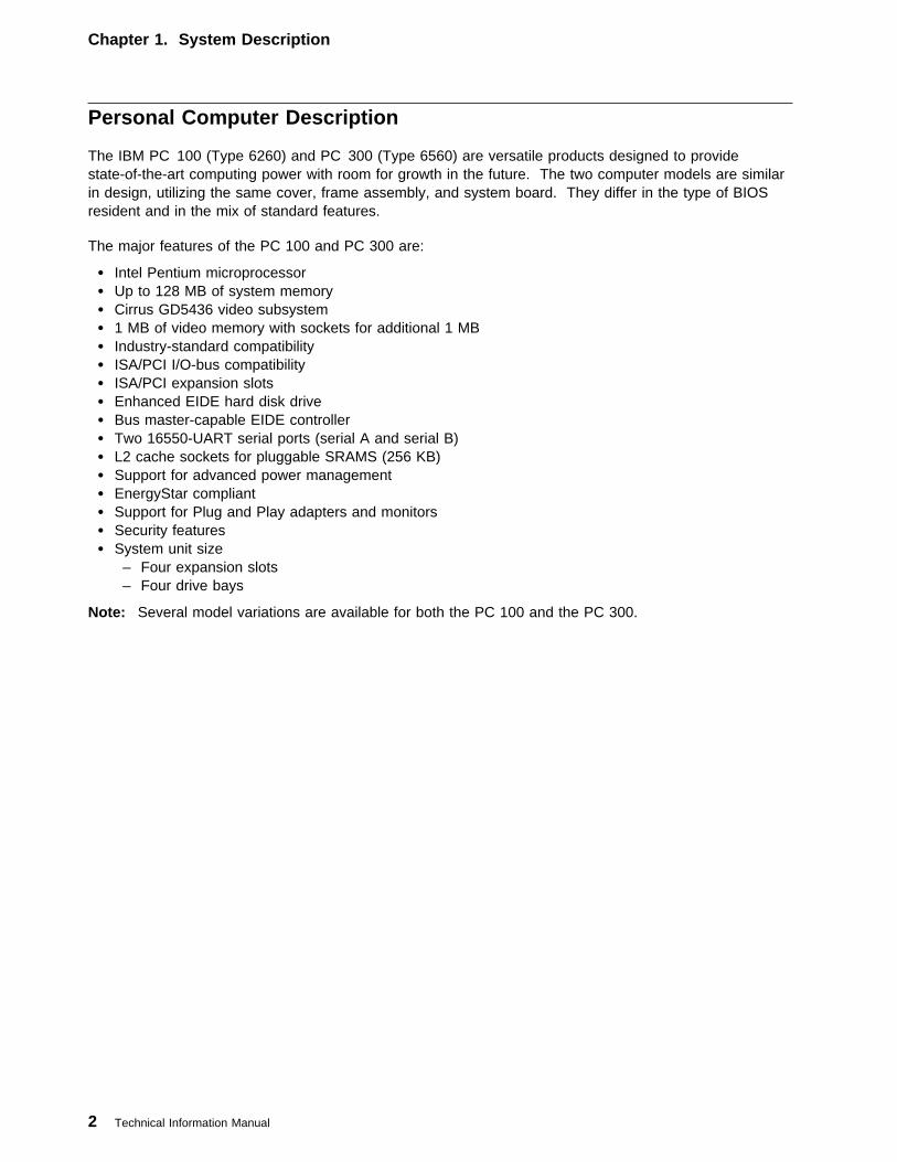
The IBM PC 100 (Type 6260) and PC 300 (Type 6560) are versatile products designed to providestate-of-the-art computing power with room for growth in the future. The two computer models are similarin design, utilizing the same cover, frame assembly, and system board. They differ in the type of BIOSresident and in the mix of standard features.
The major features of the PC 100 and PC 300 are:
� Intel Pentium microprocessor� Up to 128 MB of system memory� Cirrus GD5436 video subsystem� 1 MB of video memory with sockets for additional 1 MB
� Industry-standard compatibility� ISA/PCI I/O-bus compatibility� ISA/PCI expansion slots� Enhanced EIDE hard disk drive� Bus master-capable EIDE controller� Two 16550-UART serial ports (serial A and serial B)� L2 cache sockets for pluggable SRAMS (256 KB)� Support for advanced power management
� EnergyStar compliant� Support for Plug and Play adapters and monitors
� Security features� System unit size
– Four expansion slots– Four drive bays
Note: Several model variations are available for both the PC 100 and the PC 300.
2 Technical Information Manual
Chapter 1. System Description
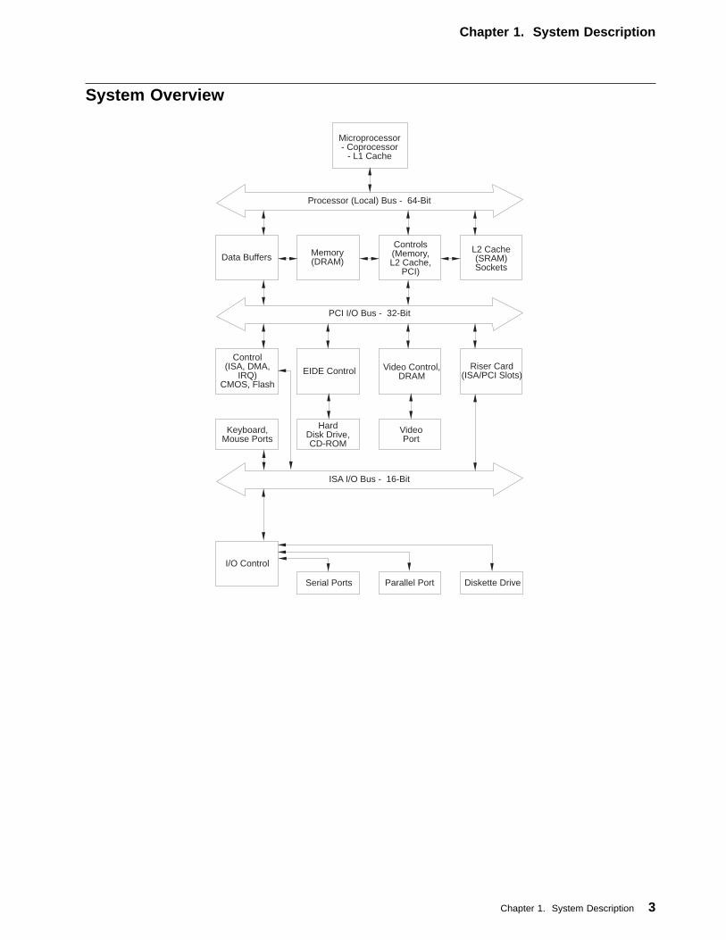
System Overview
Data Buffers
Control(ISA, DMA,
IRQ)CMOS, Flash
I/O Control
Keyboard,Mouse Ports
Serial Ports
HardDisk Drive,CD-ROM
Parallel Port
VideoPort
Diskette Drive
EIDE Control Video Control,DRAM
Riser Card(ISA/PCI Slots)
Memory(DRAM)
Controls(Memory,L2 Cache,
PCI)
L2 Cache(SRAM)Sockets
Microprocessor- Coprocessor
- L1 Cache
Processor (Local) Bus - 64-Bit
PCI I/O Bus - 32-Bit
ISA I/O Bus - 16-Bit
. .
Chapter 1. System Description 3
Chapter 1. System Description
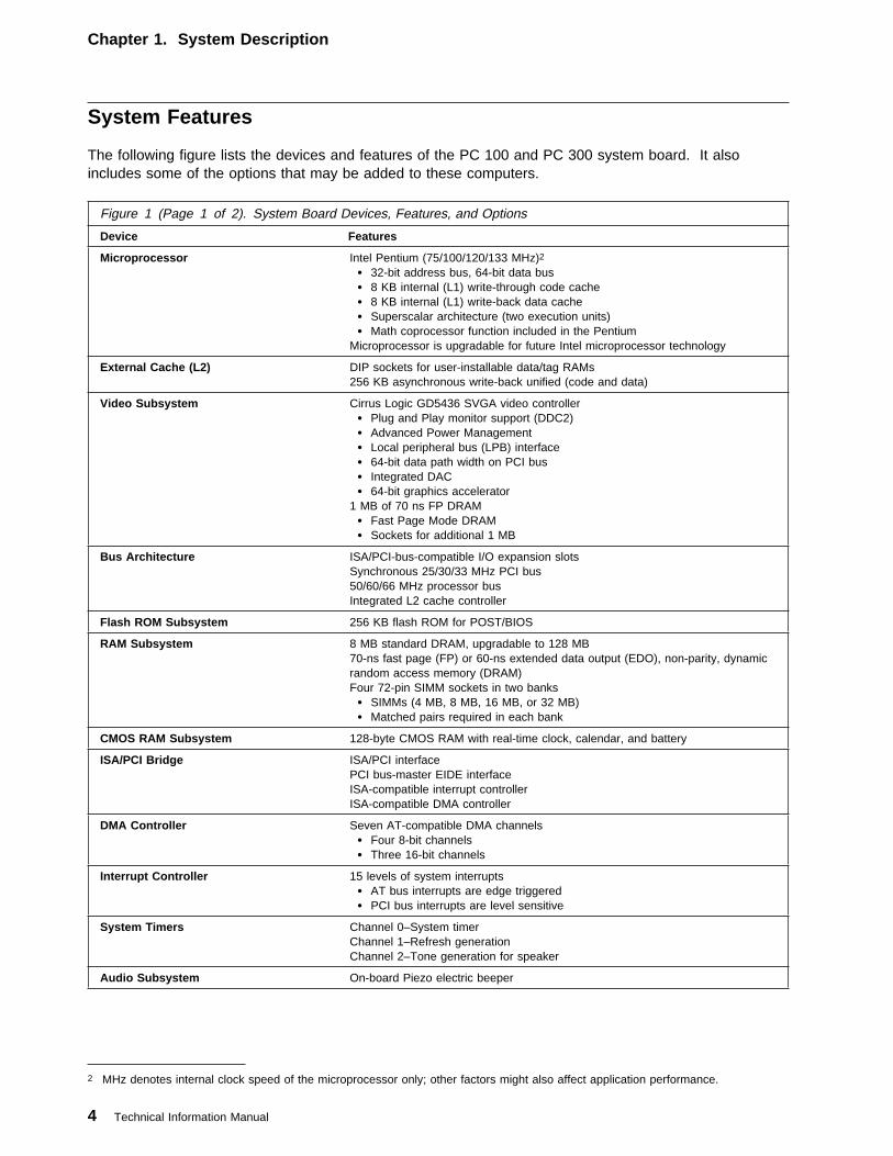
System Features
The following figure lists the devices and features of the PC 100 and PC 300 system board. It alsoincludes some of the options that may be added to these computers.
Figure 1 (Page 1 of 2). System Board Devices, Features, and Options
Device Features
Microprocessor Intel Pentium (75/100/120/133 MHz)2
� 32-bit address bus, 64-bit data bus� 8 KB internal (L1) write-through code cache� 8 KB internal (L1) write-back data cache� Superscalar architecture (two execution units)� Math coprocessor function included in the Pentium
Microprocessor is upgradable for future Intel microprocessor technology
External Cache (L2) DIP sockets for user-installable data/tag RAMs256 KB asynchronous write-back unified (code and data)
Video Subsystem Cirrus Logic GD5436 SVGA video controller� Plug and Play monitor support (DDC2)� Advanced Power Management� Local peripheral bus (LPB) interface� 64-bit data path width on PCI bus
� Integrated DAC� 64-bit graphics accelerator
1 MB of 70 ns FP DRAM� Fast Page Mode DRAM� Sockets for additional 1 MB
Bus Architecture ISA/PCI-bus-compatible I/O expansion slotsSynchronous 25/30/33 MHz PCI bus50/60/66 MHz processor busIntegrated L2 cache controller
Flash ROM Subsystem 256 KB flash ROM for POST/BIOS
RAM Subsystem 8 MB standard DRAM, upgradable to 128 MB70-ns fast page (FP) or 60-ns extended data output (EDO), non-parity, dynamicrandom access memory (DRAM)Four 72-pin SIMM sockets in two banks� SIMMs (4 MB, 8 MB, 16 MB, or 32 MB)� Matched pairs required in each bank
CMOS RAM Subsystem 128-byte CMOS RAM with real-time clock, calendar, and battery
ISA/PCI Bridge ISA/PCI interfacePCI bus-master EIDE interfaceISA-compatible interrupt controllerISA-compatible DMA controller
DMA Controller Seven AT-compatible DMA channels� Four 8-bit channels� Three 16-bit channels
Interrupt Controller 15 levels of system interrupts� AT bus interrupts are edge triggered� PCI bus interrupts are level sensitive
System Timers Channel 0–System timerChannel 1–Refresh generationChannel 2–Tone generation for speaker
Audio Subsystem On-board Piezo electric beeper
2 MHz denotes internal clock speed of the microprocessor only; other factors might also affect application performance.
4 Technical Information Manual
Chapter 1. System Description
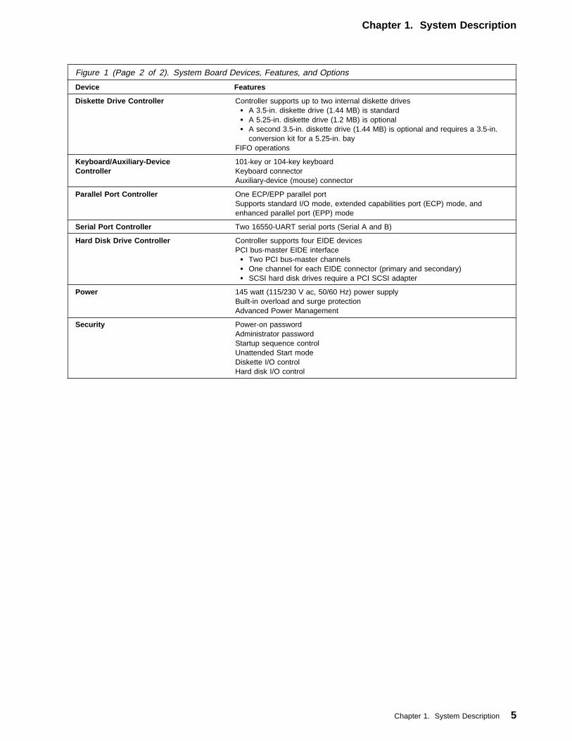
Figure 1 (Page 2 of 2). System Board Devices, Features, and Options
Device Features
Diskette Drive Controller Controller supports up to two internal diskette drives� A 3.5-in. diskette drive (1.44 MB) is standard� A 5.25-in. diskette drive (1.2 MB) is optional� A second 3.5-in. diskette drive (1.44 MB) is optional and requires a 3.5-in.
conversion kit for a 5.25-in. bay FIFO operations
Keyboard/Auxiliary-DeviceController
101-key or 104-key keyboard Keyboard connector
Auxiliary-device (mouse) connector
Parallel Port Controller One ECP/EPP parallel portSupports standard I/O mode, extended capabilities port (ECP) mode, andenhanced parallel port (EPP) mode
Serial Port Controller Two 16550-UART serial ports (Serial A and B)
Hard Disk Drive Controller Controller supports four EIDE devicesPCI bus-master EIDE interface� Two PCI bus-master channels� One channel for each EIDE connector (primary and secondary)� SCSI hard disk drives require a PCI SCSI adapter
Power 145 watt (115/230 V ac, 50/60 Hz) power supplyBuilt-in overload and surge protectionAdvanced Power Management
Security Power-on password Administrator password
Startup sequence controlUnattended Start modeDiskette I/O controlHard disk I/O control
Chapter 1. System Description 5
Chapter 1. System Description
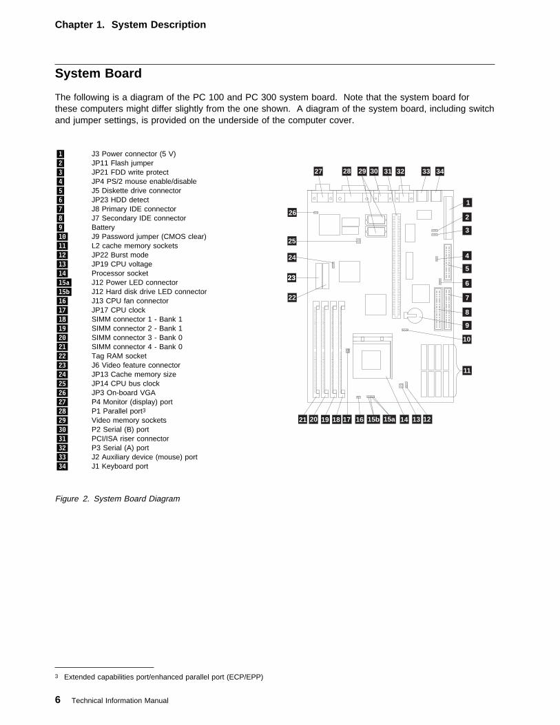
System Board
The following is a diagram of the PC 100 and PC 300 system board. Note that the system board forthese computers might differ slightly from the one shown. A diagram of the system board, including switchand jumper settings, is provided on the underside of the computer cover.
.1/ J3 Power connector (5 V)
.2/ JP11 Flash jumper
.3/ JP21 FDD write protect
.4/ JP4 PS/2 mouse enable/disable
.5/ J5 Diskette drive connector
.6/ JP23 HDD detect
.7/ J8 Primary IDE connector
.8/ J7 Secondary IDE connector
.9/ Battery
.1ð/ J9 Password jumper (CMOS clear)
.11/ L2 cache memory sockets
.12/ JP22 Burst mode
.13/ JP19 CPU voltage
.14/ Processor socket
.15a/ J12 Power LED connector
.15b/ J12 Hard disk drive LED connector
.16/ J13 CPU fan connector
.17/ JP17 CPU clock
.18/ SIMM connector 1 - Bank 1
.19/ SIMM connector 2 - Bank 1
.2ð/ SIMM connector 3 - Bank 0
.21/ SIMM connector 4 - Bank 0
.22/ Tag RAM socket
.23/ J6 Video feature connector
.24/ JP13 Cache memory size
.25/ JP14 CPU bus clock
.26/ JP3 On-board VGA
.27/ P4 Monitor (display) port
.28/ P1 Parallel port3
.29/ Video memory sockets
.3ð/ P2 Serial (B) port
.31/ PCI/ISA riser connector
.32/ P3 Serial (A) port
.33/ J2 Auxiliary device (mouse) port
.34/ J1 Keyboard port
Figure 2. System Board Diagram
25
1
33 34
2
3
4
5
6
7
8
9
10
1213
11
15a15b 14161718192021
22
2323
24
26
27 29 30 31 323228
3 Extended capabilities port/enhanced parallel port (ECP/EPP)
6 Technical Information Manual

Chapter 1. System Description
System Address Maps
Memory Map
The first 640 KB of system board RAM is mapped starting at address 0000000h. A 256-byte area and a 1KB area of this RAM are reserved for BIOS data areas. Memory can be mapped differently if POSTdetects an error. See the section about BIOS data areas in the IBM Personal System/2 and PersonalComputer BIOS Interface Technical Reference for details.
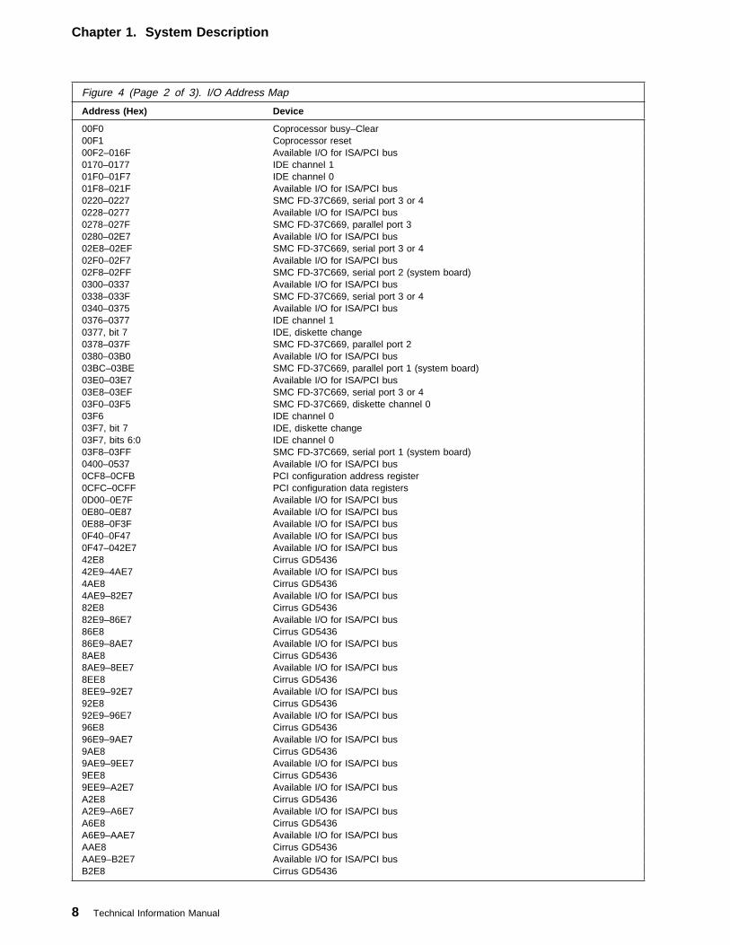
Input/Output Address Map
The following figures list the system board I/O address maps. Any addresses that are not shown arereserved.
Figure 3. System Memory Map
Address Range(Decimal)
Address Range(Hex)
Size Description
1024K–131072K 100000–8000000 127M Extended memory
960K–1023K F0000–FFFFF 64K System BIOS
944K–959K EC000–EFFFF 16K Available
936K–943K EA000–EBFFF 8K ESCD (Plug and Play configuration area)
928K–935K E8000-E9FFF 8K Available
896K–927K E0000–E7FFF 32K BIOS reserved
800K–895K C8000–DFFFF 96K Available HI DOS memory (open to ISA and PCI bus)
640K–799K A0000–C7FFF 160K Video memory and BIOS
512K–639K 80000–9FFFF 128K Extended
0K–511K 00000–7FFFF 512K DOS applications (conventional)
Figure 4 (Page 1 of 3). I/O Address Map
Address (Hex) Device
0000–000F DMA 10020–003F Interrupt controller 10040–0043 Timer 10044–0047 Available I/O for ISA/PCI bus0048–004B Timer 2004C–005F Available I/O for ISA/PCI bus0060 Keyboard controller data byte0061 System Port B0062–0063 Available I/O for ISA/PCI bus0064 Keyboard controller, command and status byte0065–006F Available I/O for ISA/PCI bus0070, bit 7 Enable/disable NMI0070, bits 6:0 Real time clock address0071 Real time clock data0072–0077 Available I/O for ISA/PCI bus0078 Reserved-system board setup0079 Reserved-system board setup007A–007F Available I/O for ISA/PCI bus0080 POST checkpoint register0080-008F DMA page register0090–009F Available I/O for ISA/PCI bus00A0–00BF Interrupt controller 200C0–00DE DMA 200DF–00EF Available I/O for ISA/PCI bus
Chapter 1. System Description 7
Chapter 1. System Description
Figure 4 (Page 2 of 3). I/O Address Map
Address (Hex) Device
00F0 Coprocessor busy–Clear00F1 Coprocessor reset00F2–016F Available I/O for ISA/PCI bus0170–0177 IDE channel 101F0–01F7 IDE channel 001F8–021F Available I/O for ISA/PCI bus0220–0227 SMC FD-37C669, serial port 3 or 40228–0277 Available I/O for ISA/PCI bus0278–027F SMC FD-37C669, parallel port 30280–02E7 Available I/O for ISA/PCI bus02E8–02EF SMC FD-37C669, serial port 3 or 402F0–02F7 Available I/O for ISA/PCI bus02F8–02FF SMC FD-37C669, serial port 2 (system board)0300–0337 Available I/O for ISA/PCI bus0338–033F SMC FD-37C669, serial port 3 or 40340–0375 Available I/O for ISA/PCI bus0376–0377 IDE channel 10377, bit 7 IDE, diskette change0378–037F SMC FD-37C669, parallel port 20380–03B0 Available I/O for ISA/PCI bus03BC–03BE SMC FD-37C669, parallel port 1 (system board)03E0–03E7 Available I/O for ISA/PCI bus03E8–03EF SMC FD-37C669, serial port 3 or 403F0–03F5 SMC FD-37C669, diskette channel 003F6 IDE channel 003F7, bit 7 IDE, diskette change03F7, bits 6:0 IDE channel 003F8–03FF SMC FD-37C669, serial port 1 (system board)0400–0537 Available I/O for ISA/PCI bus0CF8–0CFB PCI configuration address register0CFC–0CFF PCI configuration data registers0D00–0E7F Available I/O for ISA/PCI bus0E80–0E87 Available I/O for ISA/PCI bus0E88–0F3F Available I/O for ISA/PCI bus0F40–0F47 Available I/O for ISA/PCI bus0F47–042E7 Available I/O for ISA/PCI bus42E8 Cirrus GD543642E9–4AE7 Available I/O for ISA/PCI bus4AE8 Cirrus GD54364AE9–82E7 Available I/O for ISA/PCI bus82E8 Cirrus GD543682E9–86E7 Available I/O for ISA/PCI bus86E8 Cirrus GD543686E9–8AE7 Available I/O for ISA/PCI bus8AE8 Cirrus GD54368AE9–8EE7 Available I/O for ISA/PCI bus8EE8 Cirrus GD54368EE9–92E7 Available I/O for ISA/PCI bus92E8 Cirrus GD543692E9–96E7 Available I/O for ISA/PCI bus96E8 Cirrus GD543696E9–9AE7 Available I/O for ISA/PCI bus9AE8 Cirrus GD54369AE9–9EE7 Available I/O for ISA/PCI bus9EE8 Cirrus GD54369EE9–A2E7 Available I/O for ISA/PCI busA2E8 Cirrus GD5436A2E9–A6E7 Available I/O for ISA/PCI busA6E8 Cirrus GD5436A6E9–AAE7 Available I/O for ISA/PCI busAAE8 Cirrus GD5436AAE9–B2E7 Available I/O for ISA/PCI busB2E8 Cirrus GD5436
8 Technical Information Manual
Chapter 1. System Description
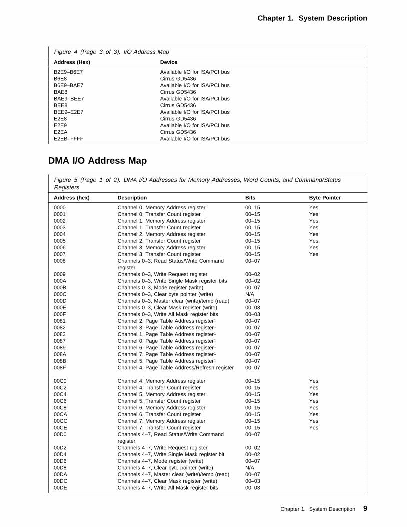
DMA I/O Address Map
Figure 4 (Page 3 of 3). I/O Address Map
Address (Hex) Device
B2E9–B6E7 Available I/O for ISA/PCI busB6E8 Cirrus GD5436B6E9–BAE7 Available I/O for ISA/PCI busBAE8 Cirrus GD5436BAE9–BEE7 Available I/O for ISA/PCI busBEE8 Cirrus GD5436BEE9–E2E7 Available I/O for ISA/PCI busE2E8 Cirrus GD5436E2E9 Available I/O for ISA/PCI busE2EA Cirrus GD5436E2EB–FFFF Available I/O for ISA/PCI bus
Figure 5 (Page 1 of 2). DMA I/O Addresses for Memory Addresses, Word Counts, and Command/StatusRegisters
Address (hex) Description Bits Byte Pointer
0000 Channel 0, Memory Address register 00–15 Yes0001 Channel 0, Transfer Count register 00–15 Yes0002 Channel 1, Memory Address register 00–15 Yes0003 Channel 1, Transfer Count register 00–15 Yes0004 Channel 2, Memory Address register 00–15 Yes0005 Channel 2, Transfer Count register 00–15 Yes0006 Channel 3, Memory Address register 00–15 Yes0007 Channel 3, Transfer Count register 00–15 Yes0008 Channels 0–3, Read Status/Write Command
register 00–07
0009 Channels 0–3, Write Request register 00–02 000A Channels 0–3, Write Single Mask register bits 00–02 000B Channels 0–3, Mode register (write) 00–07 000C Channels 0–3, Clear byte pointer (write) N/A 000D Channels 0–3, Master clear (write)/temp (read) 00–07 000E Channels 0–3, Clear Mask register (write) 00–03000F Channels 0–3, Write All Mask register bits 00–030081 Channel 2, Page Table Address registerñ 00–07 0082 Channel 3, Page Table Address registerñ 00–07 0083 Channel 1, Page Table Address registerñ 00–07 0087 Channel 0, Page Table Address registerñ 00–07 0089 Channel 6, Page Table Address registerñ 00–07 008A Channel 7, Page Table Address registerñ 00–07 008B Channel 5, Page Table Address registerñ 00–07 008F Channel 4, Page Table Address/Refresh register 00–07
00C0 Channel 4, Memory Address register 00–15 Yes00C2 Channel 4, Transfer Count register 00–15 Yes00C4 Channel 5, Memory Address register 00–15 Yes00C6 Channel 5, Transfer Count register 00–15 Yes00C8 Channel 6, Memory Address register 00–15 Yes00CA Channel 6, Transfer Count register 00–15 Yes00CC Channel 7, Memory Address register 00–15 Yes00CE Channel 7, Transfer Count register 00–15 Yes00D0 Channels 4–7, Read Status/Write Command
register00–07
00D2 Channels 4–7, Write Request register 00–02 00D4 Channels 4–7, Write Single Mask register bit 00–02 00D6 Channels 4–7, Mode register (write) 00–07 00D8 Channels 4–7, Clear byte pointer (write) N/A 00DA Channels 4–7, Master clear (write)/temp (read) 00–07 00DC Channels 4–7, Clear Mask register (write) 00–03 00DE Channels 4–7, Write All Mask register bits 00–03
Chapter 1. System Description 9
Chapter 1. System Description
IRQ and DMA Channel Assignments
The following figures list the interrupt request (IRQ) and direct memory access (DMA) channelassignments.
Interrupt Request Assignments (IRQ)
DMA Channel Assignments
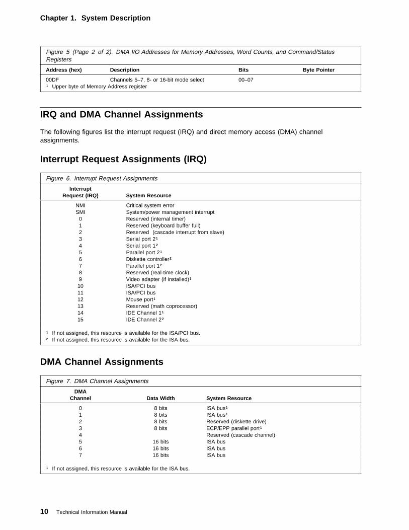
Figure 5 (Page 2 of 2). DMA I/O Addresses for Memory Addresses, Word Counts, and Command/StatusRegisters
Address (hex) Description Bits Byte Pointer
00DF Channels 5–7, 8- or 16-bit mode select 00–07 ñ Upper byte of Memory Address register
Figure 6. Interrupt Request Assignments
InterruptRequest (IRQ)
System Resource
NMI Critical system errorSMI System/power management interrupt
0 Reserved (internal timer)1 Reserved (keyboard buffer full)2 Reserved (cascade interrupt from slave)3 Serial port 2ñ4 Serial port 1ò5 Parallel port 2ñ6 Diskette controllerò7 Parallel port 1ò8 Reserved (real-time clock)9 Video adapter (if installed)ñ
10 ISA/PCI bus11 ISA/PCI bus12 Mouse portñ13 Reserved (math coprocessor)14 IDE Channel 1ñ15 IDE Channel 2ò
ñ If not assigned, this resource is available for the ISA/PCI bus.ò If not assigned, this resource is available for the ISA bus.
Figure 7. DMA Channel Assignments
DMAChannel
Data Width
System Resource
0 8 bits ISA busñ1 8 bits ISA busñ2 8 bits Reserved (diskette drive)3 8 bits ECP/EPP parallel portñ4 Reserved (cascade channel)5 16 bits ISA bus6 16 bits ISA bus7 16 bits ISA bus
ñ If not assigned, this resource is available for the ISA bus.
10 Technical Information Manual
Chapter 1. System Description
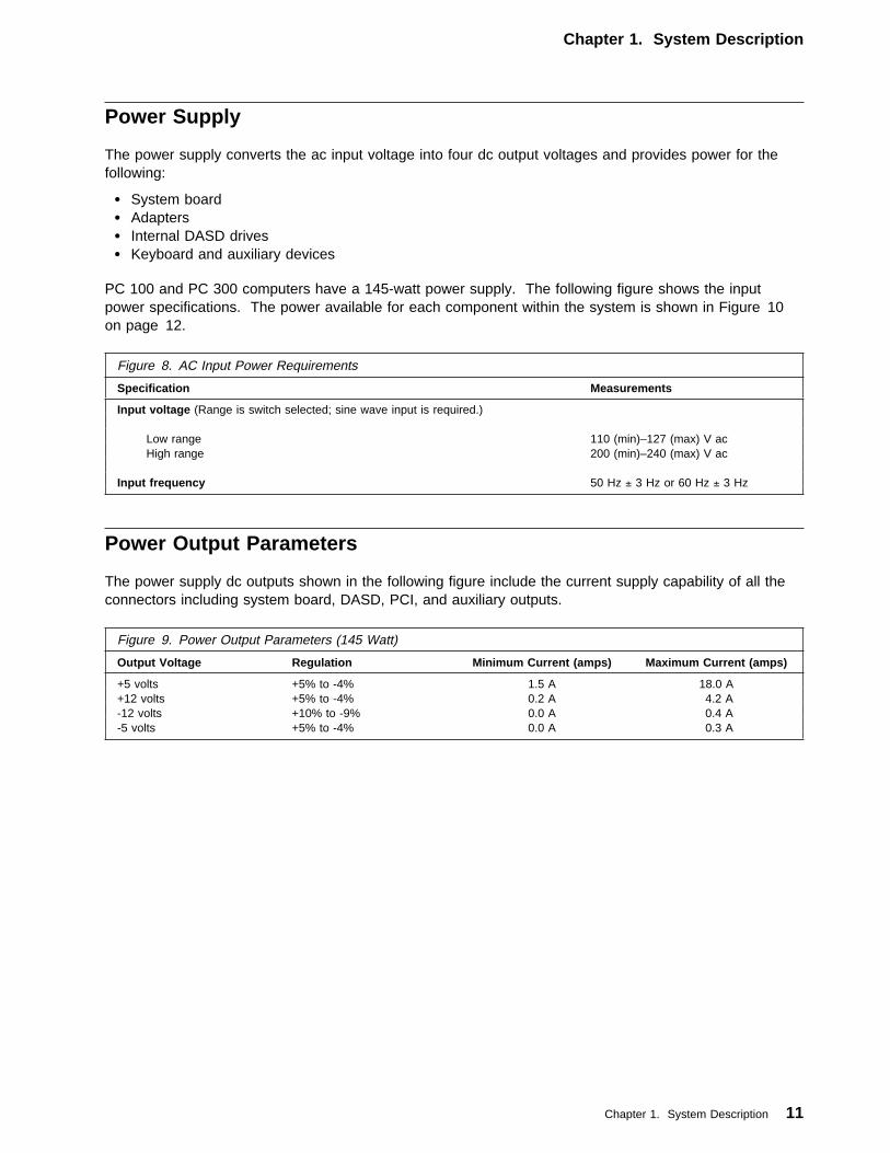
Power Supply
The power supply converts the ac input voltage into four dc output voltages and provides power for thefollowing:
� System board � Adapters� Internal DASD drives� Keyboard and auxiliary devices
PC 100 and PC 300 computers have a 145-watt power supply. The following figure shows the inputpower specifications. The power available for each component within the system is shown in Figure 10on page 12.
Power Output Parameters
The power supply dc outputs shown in the following figure include the current supply capability of all theconnectors including system board, DASD, PCI, and auxiliary outputs.
Figure 8. AC Input Power Requirements
Specification Measurements
Input voltage (Range is switch selected; sine wave input is required.) Low range 110 (min)–127 (max) V ac High range 200 (min)–240 (max) V ac Input frequency 50 Hz ± 3 Hz or 60 Hz ± 3 Hz
Figure 9. Power Output Parameters (145 Watt)
Output Voltage Regulation Minimum Current (amps) Maximum Current (amps)
+5 volts +5% to -4% 1.5 A 18.0 A+12 volts +5% to -4% 0.2 A 4.2 A-12 volts +10% to -9% 0.0 A 0.4 A-5 volts +5% to -4% 0.0 A 0.3 A
Chapter 1. System Description 11

Chapter 1. System Description
Component Outputs
The power supply provides separate voltage sources for the system board and internal storage devices.The following figure shows the approximate power that is provided for system components. Manycomponents draw less current than the maximum shown.
Note: Some adapters and hard disk drives draw more current than the recommended limits. Theseadapters and drives can be installed in the system; however, the power supply will shut down if thetotal power used exceeds the maximum power that is available.
Output Protection
The power supply protects against output overcurrent, overvoltage, and short circuits. Please see thepower supply specifications for details.
A short circuit that is placed on any dc output (between outputs or between an output and dc return)latches all dc outputs into a shutdown state, with no damage to the power supply.
If this shutdown state occurs, the power supply returns to normal operation only after the fault has beenremoved and the power switch has been turned off for at least one second.
If an overvoltage fault occurs (in the power supply), the power supply latches all dc outputs into ashutdown state before any output exceeds 130% of the nominal value of the power supply.
Figure 10. Component Maximum Current
Supply Voltage (V dc) Maximum Current (mA) Regulation Limits
System Board:
+5.0 V dc 4000 mA +5.0% to −5.0%+12.0 V dc 25.0 mA +5.0% to −5.0%−12.0 V dc 25.0 mA +10.0% to −9.0%
Keyboard Port:
+5.0 V dc 275 mA +5.0% to −5.0%
Auxiliary-Device (Mouse) Port:
+5.0 V dc 300 mA +5.0% to −5.0%
AT-Bus Adapters (Per Slot):
+5.0 V dc 4500 mA +5.0% to −5.0%−5.0 V dc 200 mA +5.0% to −5.0%
+12.0 V dc 1500 mA +5.0% to −5.0%−12.0 V dc 300 mA +5.0% to −5.0%
PCI-Bus Adapters (Per Slot)
+5.0 V dc 5000 mA +5.0% to −4.0%
Internal DASD:
+5.0 V dc 1400 mA +5.0% to −5.0%
+12.0 V dc 1500 mA +5.0% to −5.0%
12 Technical Information Manual
Chapter 1. System Description
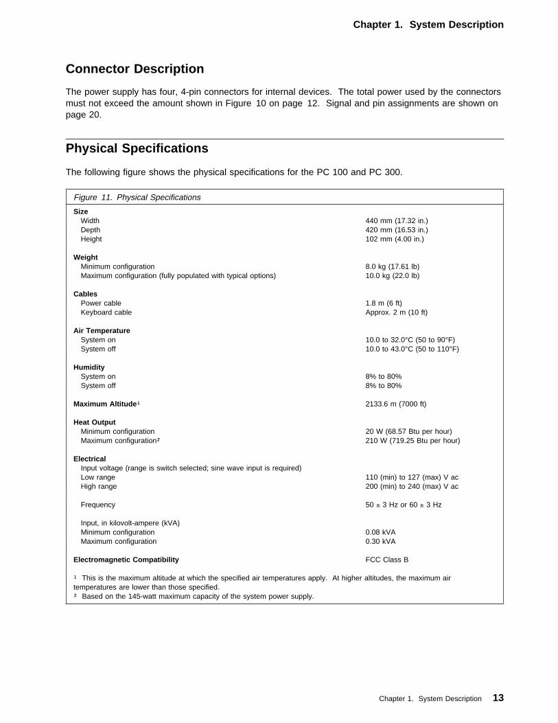
Connector Description
The power supply has four, 4-pin connectors for internal devices. The total power used by the connectorsmust not exceed the amount shown in Figure 10 on page 12. Signal and pin assignments are shown onpage 20.
Physical Specifications
The following figure shows the physical specifications for the PC 100 and PC 300.
Figure 11. Physical Specifications
Size Width 440 mm (17.32 in.) Depth 420 mm (16.53 in.) Height 102 mm (4.00 in.) Weight Minimum configuration 8.0 kg (17.61 lb)
Maximum configuration (fully populated with typical options) 10.0 kg (22.0 lb) Cables Power cable 1.8 m (6 ft) Keyboard cable Approx. 2 m (10 ft) Air Temperature System on 10.0 to 32.0°C (50 to 90°F) System off 10.0 to 43.0°C (50 to 110°F) Humidity System on 8% to 80% System off 8% to 80% Maximum Altitude ñ 2133.6 m (7000 ft) Heat Output Minimum configuration 20 W (68.57 Btu per hour) Maximum configurationò 210 W (719.25 Btu per hour) Electrical
Input voltage (range is switch selected; sine wave input is required) Low range 110 (min) to 127 (max) V ac High range 200 (min) to 240 (max) V ac Frequency 50 ± 3 Hz or 60 ± 3 Hz
Input, in kilovolt-ampere (kVA) Minimum configuration 0.08 kVA Maximum configuration 0.30 kVA Electromagnetic Compatibility FCC Class B ñ This is the maximum altitude at which the specified air temperatures apply. At higher altitudes, the maximum airtemperatures are lower than those specified.ò Based on the 145-watt maximum capacity of the system power supply.
Chapter 1. System Description 13

Chapter 1. System Description
Advanced Power Management (APM)
The PC 100 and PC 300 come with built-in energy-saving capabilities. Advanced Power Management(APM) is a feature that reduces the power consumption of systems when they are not being used. APM,when enabled, initiates reduced-power modes for the monitor, microprocessor, and hard disk drive after aspecified period of inactivity.
The following figure summarizes APM modes.
The BIOS supports APM Version 1.2. This enables the system to enter a power-managed state, whichreduces the power drawn from the ac wall outlet. Advanced Power Management is enabled through theConfiguration/Setup Utility program and is controlled by the individual operating system.
Figure 12. Advanced Power Management Modes
Mode Power Response
On (Ready) System is at full power Standard operation On (Standby) System is at reduced power Any use of keyboard, mouse, or hard disk drive restores full
power Off System is powered off Power switch restores full power
14 Technical Information Manual
Chapter 2. Connectors and Jumpers
Chapter 2. Connectors and Jumpers
System Board Connectors . . . . . . . . . . . . . . . . . . . . . . . . . . . . . . . . . . . . . . . . . . . . 16Diskette Drive Connector . . . . . . . . . . . . . . . . . . . . . . . . . . . . . . . . . . . . . . . . . . . . 16Hard Disk Drive Connectors (Primary/Secondary) . . . . . . . . . . . . . . . . . . . . . . . . . . . . . 17ISA Connectors . . . . . . . . . . . . . . . . . . . . . . . . . . . . . . . . . . . . . . . . . . . . . . . . . 18PCI Connectors . . . . . . . . . . . . . . . . . . . . . . . . . . . . . . . . . . . . . . . . . . . . . . . . . 19Power Supply Connectors . . . . . . . . . . . . . . . . . . . . . . . . . . . . . . . . . . . . . . . . . . . 20System Board Memory Connectors . . . . . . . . . . . . . . . . . . . . . . . . . . . . . . . . . . . . . . 21Video Feature Connector . . . . . . . . . . . . . . . . . . . . . . . . . . . . . . . . . . . . . . . . . . . . 22
I/O Connectors . . . . . . . . . . . . . . . . . . . . . . . . . . . . . . . . . . . . . . . . . . . . . . . . . . . 23Keyboard and Auxiliary-Device (Mouse) Connectors . . . . . . . . . . . . . . . . . . . . . . . . . . . . 23Serial Port Connectors . . . . . . . . . . . . . . . . . . . . . . . . . . . . . . . . . . . . . . . . . . . . . 24
Serial-Port Setup . . . . . . . . . . . . . . . . . . . . . . . . . . . . . . . . . . . . . . . . . . . . . . . 24Parallel Port Connector . . . . . . . . . . . . . . . . . . . . . . . . . . . . . . . . . . . . . . . . . . . . . 25
Parallel-Port Setup . . . . . . . . . . . . . . . . . . . . . . . . . . . . . . . . . . . . . . . . . . . . . . 26Parallel-Port Modes . . . . . . . . . . . . . . . . . . . . . . . . . . . . . . . . . . . . . . . . . . . . . 27
Monitor Connector . . . . . . . . . . . . . . . . . . . . . . . . . . . . . . . . . . . . . . . . . . . . . . . . 27
Copyright IBM Corp. August 1996 15

Chapter 2. Connectors and Jumpers
System Board Connectors
The following figures show the connectors that are available on the system board and riser card.
Diskette Drive Connector
PC 100 and PC 300 computers have a 34-pin connector that supports the attachment of up to two diskettedrives. The following figure shows the signal and pin assignments for the system board diskette driveconnector.
Figure 13. Diskette Drive Connector Signal and Pin Assignments
Pin Signal Pin Signal
1 Ground 2 High density select3 Ground 4 Not connected5 Ground 6 -Drive type7 Ground 8 -Index9 Ground 10 -Motor enable 0
11 Ground 12 -Drive select 113 Ground 14 -Drive select 015 Ground 16 -Motor enable 117 Ground 18 -Direction in19 Ground 20 -Step21 Ground 22 -Write data23 Ground 24 -Write enable25 Ground 26 -Track 027 Ground 28 -Write protect29 n/c or key 30 -Read data31 Ground 32 -Head 1 select33 Ground 34 -Diskette change
16 Technical Information Manual

Chapter 2. Connectors and Jumpers
Hard Disk Drive Connectors (Primary/Secondary)
PC 100 and PC 300 computers have two EIDE connectors for attaching IDE devices (such as hard diskdrives and CD-ROM drives). The signals that are provided by these connectors include the 16-bit databus, address lines A0 to A2, IRQ, and -IO CS16. These signals operate in the same way as the normalI/O-channel signals. The interface to the hard disk drive complies with ANSI ATA-2 (AT Attachment).
The address decode logic for the hard disk drive is on the system board. On a valid decode of A0 throughA15 equal to 01F0h through 01F7h, -HFCS0 (0170h through 0177h, -HFCS2 for a secondary hard diskdrive) goes active. On a valid decode of A0 through A15 equal to 03F6h through 03F7h, -HFCS1 (0376hthrough 0377h, -HFCS3 for a secondary hard disk drive) goes active.
The following figure shows the signal and pin assignments for the EIDE connectors.
Figure 14. EIDE Connector Signal and Pin Assignments
Pin Signal Pin Signal
1 -RESET 2 Ground 3 Data bus bit 7 4 Data bus bit 8 5 Data bus bit 6 6 Data bus bit 9 7 Data bus bit 5 8 Data bus bit 10 9 Data bus bit 4 10 Data bus bit 1111 Data bus bit 3 12 Data bus bit 1213 Data bus bit 2 14 Data bus bit 1315 Data bus bit 1 16 Data bus bit 1417 Data bus bit 0 18 Data bus bit 1519 Ground 20 Key (Reserved)21 DRQ0/DRQ1 22 Ground23 -IO Write 24 Ground25 -IO Read 26 Ground27 IO Channel Ready 28 VCC pullup29 DACK0/DACK1 30 Ground31 IRQ14/IRQ15 32 VCC pullup33 Device address A1 34 Ground35 Device address A0 36 Device address A237 -HFCS0 38 -HFCS139 Activity # 40 Ground
Chapter 2. Connectors and Jumpers 17

Chapter 2. Connectors and Jumpers
ISA Connectors
The I/O channel (ISA bus) is buffered to provide sufficient drive for the 98-pin connectors, assuming twolow-power Schottky (LS) loads per slot.
The following figure shows the signal and pin assignments for the I/O channel connectors.
B1
B10
B31
A1
A10
A31
Rear Panel
B20 A20
D1
D10
C1
C10
C18D18
-I/O CH CKSD7SD6SD5SD4SD3SD2SD1SD0I/O CH RDYAENSA19SA18SA17SA16SA15SA14SA13SA12SA11SA10SA9SA8SA7SA6SA5SA4SA3SA2SA1SA0
-MEM CS16-I/O CS16IRQ10IRQ11IRQ12IRQ15IRQ14-DACK0DRQ0-DACK5DRQ5-DACK6DRQ6-DACK7DRQ7+5V dc-MASTERGround
-SBHELA23LA22LA21LA20LA19LA18LA17-MEMR-MEMWSD08SD09SD10SD11SD12SD13SD14SD15
GroundRESET DRV+5 V dcIRQ 2-5 V dcDRQ2-12 V dc-0WS+12 V dcGround-SMEMW-SMEMR-IOW-IOR-DACK3DRQ3-DACK1DRQ1-REFRESHCLKIRQ7IRQ6IRQ5IRQ4IRQ3-DACK2TCBALE+5 V dcOSCGroun
Figure 15. I/O Channel (ISA Bus) Connector
18 Technical Information Manual
Chapter 2. Connectors and Jumpers
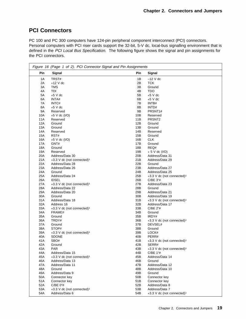
PCI Connectors
PC 100 and PC 300 computers have 124-pin peripheral component interconnect (PCI) connectors.Personal computers with PCI riser cards support the 32-bit, 5-V dc, local-bus signalling environment that isdefined in the PCI Local Bus Specification. The following figure shows the signal and pin assignments forthe PCI connectors.
Figure 16 (Page 1 of 2). PCI Connector Signal and Pin Assignments
Pin Signal Pin Signal
1A TRST# 1B −12 V dc 2A +12 V dc 2B TCK 3A TMS 3B Ground 4A TDI 4B TDO 5A +5 V dc 5B +5 V dc 6A INTA# 6B +5 V dc 7A INTC# 7B INTB# 8A +5 V dc 8B INTD# 9A Reserved 9B PRSNT1#10A +5 V dc (I/O) 10B Reserved11A Reserved 11B PRSNT212A Ground 12B Ground13A Ground 13B Ground14A Reserved 14B Reserved15A RST# 15B Ground16A +5 V dc (I/O) 16B CLK17A GNT# 17B Ground18A Ground 18B REQ#19A Reserved 19B + 5 V dc (I/O)20A Address/Data 30 20B Address/Data 3121A +3.3 V dc (not connected)ñ 21B Address/Data 2922A Address/Data 28 22B Ground23A Address/Data 26 23B Address/Data 2724A Ground 24B Address/Data 2525A Address/Data 24 25B +3.3 V dc (not connected)ñ26A IDSEL 26B C/BE 3“#27A +3.3 V dc (not connected)ñ 27B Address/Data 2328A Address/Data 22 28B Ground29A Address/Data 20 29B Address/Data 2130A Ground 30B Address/Data 1931A Address/Data 18 31B +3.3 V dc (not connected)ñ32A Address 16 32B Address/Data 1733A +3.3 V dc (not connected)ñ 33B C/BE 2“#34A FRAME# 34B Ground35A Ground 35B IRDY#36A TRDY# 36B +3.3 V dc (not connected)ñ37A Ground 37B DEVSEL#38A STOP# 38B Ground39A +3.3 V dc (not connected)ñ 39B LOCK#40A SDONE 40B PERR#41A SBO# 41B +3.3 V dc (not connected)ñ42A Ground 42B SERR#43A PAR 43B +3.3 V dc (not connected)ñ44A Address/Data 15 44B C/BE 1“#45A +3.3 V dc (not connected)ñ 45B Address/Data 1446A Address/Data 13 46B Ground47A Address/Data 11 47B Address/Data 1248A Ground 48B Address/Data 1049A Address/Data 9 49B Ground50A Connector key 50B Connector key51A Connector key 51B Connector key52A C/BE 0“# 52B Address/Data 853A +3.3 V dc (not connected)ñ 53B Address/Data 754A Address/Data 6 54B +3.3 V dc (not connected)ñ
Chapter 2. Connectors and Jumpers 19
Chapter 2. Connectors and Jumpers
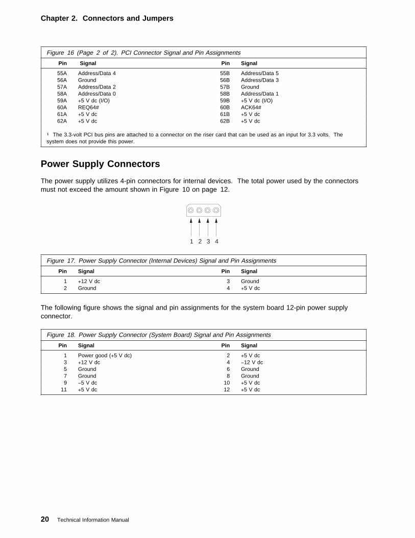
Power Supply Connectors
The power supply utilizes 4-pin connectors for internal devices. The total power used by the connectorsmust not exceed the amount shown in Figure 10 on page 12.
4321
The following figure shows the signal and pin assignments for the system board 12-pin power supplyconnector.
Figure 16 (Page 2 of 2). PCI Connector Signal and Pin Assignments
Pin Signal Pin Signal
55A Address/Data 4 55B Address/Data 556A Ground 56B Address/Data 357A Address/Data 2 57B Ground58A Address/Data 0 58B Address/Data 159A +5 V dc (I/O) 59B +5 V dc (I/O)60A REQ64# 60B ACK64#61A +5 V dc 61B +5 V dc62A +5 V dc 62B +5 V dc
ñ The 3.3-volt PCI bus pins are attached to a connector on the riser card that can be used as an input for 3.3 volts. Thesystem does not provide this power.
Figure 17. Power Supply Connector (Internal Devices) Signal and Pin Assignments
Pin Signal Pin Signal
1 +12 V dc 3 Ground2 Ground 4 +5 V dc
Figure 18. Power Supply Connector (System Board) Signal and Pin Assignments
Pin Signal Pin Signal
1 Power good (+5 V dc) 2 +5 V dc 3 +12 V dc 4 −12 V dc 5 Ground 6 Ground 7 Ground 8 Ground 9 −5 V dc 10 +5 V dc11 +5 V dc 12 +5 V dc
20 Technical Information Manual

Chapter 2. Connectors and Jumpers
System Board Memory Connectors
The following figure shows the signal and pin assignments for the 72-pin system board memoryconnectors. Data bits 0 through 15 are the low word, and data bits 16 through 31 are the high word.
Figure 19. System Board Memory Connector Signal and Pin Assignments
Pin Signal Pin Signal
1 Ground 37 Parity 1 not used 2 Data 0 38 Parity 3 not used 3 Data 16 39 Ground 4 Data 1 40 Column address strobe 0 5 Data 17 41 Column address strobe 2 6 Data 2 42 Column address strobe 3 7 Data 18 43 Column address strobe 1 8 Data 3 44 Row address strobe 0 9 Data 19 45 Row address strobe 110 +5 V dc 46 Reserved11 Reserved 47 Write enable12 Address 0 48 Reserved13 Address 1 49 Data 814 Address 2 50 Data 2415 Address 3 51 Data 916 Address 4 52 Data 2517 Address 5 53 Data 1018 Address 6 54 Data 2619 Address 10 55 Data 1120 Data 4 56 Data 2721 Data 20 57 Data 1222 Data 5 58 Data 2823 Data 21 59 +5 V dc24 Data 6 60 Data 2925 Data 22 61 Data 1326 Data 7 62 Data 3027 Data 23 63 Data 1428 Address 7 64 Data 3129 Reserved 65 Data 1530 +5 V dc 66 Reserved31 Address 8 67 Reserved32 Address 9 68 Reserved33 Row address strobe 3 69 Reserved34 Row address strobe 2 70 Reserved35 Parity 2 not used 71 Reserved36 Parity 0 not used 72 Ground
Chapter 2. Connectors and Jumpers 21

Chapter 2. Connectors and Jumpers
Video Feature Connector
PC 100 and PC 300 computers have a 26-pin connector that supports the attachment of additional videofeatures. The following figure shows the signal and pin assignments for the video feature connector.
Figure 20. Video Feature Connector
Pin Signal Pin Signal
1 Ground 2 Data 03 Ground 4 Data 15 Ground 6 Data 27 Data enable 8 Data 39 Sync enable 10 Data 4
11 PCLK enable 12 Data 513 DDCCLK 14 Data 615 Ground 16 Data 717 Ground 18 PCLK19 Ground 20 BLANK21 Ground 22 HSYNC23 VMCLK 24 VSYNC25 DDC Data 26 Ground
22 Technical Information Manual
Chapter 2. Connectors and Jumpers
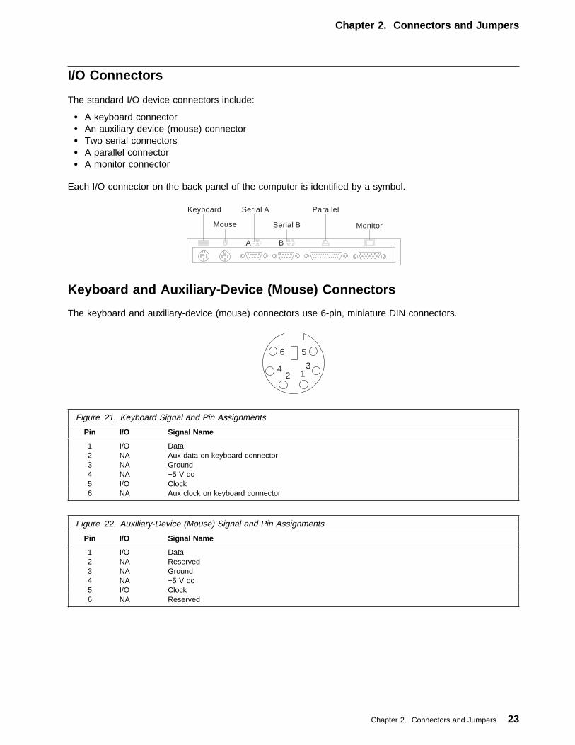
I/O Connectors
The standard I/O device connectors include:
� A keyboard connector� An auxiliary device (mouse) connector� Two serial connectors� A parallel connector� A monitor connector
Each I/O connector on the back panel of the computer is identified by a symbol.
Keyboard
Mouse
Serial A
A B
Parallel
MonitorSerial B
Keyboard and Auxiliary-Device (Mouse) Connectors
The keyboard and auxiliary-device (mouse) connectors use 6-pin, miniature DIN connectors.
6
42 1
3
5
Figure 21. Keyboard Signal and Pin Assignments
Pin I/O Signal Name
1 I/O Data2 NA Aux data on keyboard connector3 NA Ground4 NA +5 V dc5 I/O Clock6 NA Aux clock on keyboard connector
Figure 22. Auxiliary-Device (Mouse) Signal and Pin Assignments
Pin I/O Signal Name
1 I/O Data2 NA Reserved3 NA Ground4 NA +5 V dc5 I/O Clock6 NA Reserved
Chapter 2. Connectors and Jumpers 23

Chapter 2. Connectors and Jumpers
Serial Port Connectors
The two serial connectors on the back of the computer use a 9-pin, male, D-shell connector and pinassignments defined for RS-232D. The voltage levels are EIA only. Current loop interface is notsupported.
1 5
6 9
The following figure shows the signal and pin assignments for the serial port connector in acommunication environment.
Use Serial A or Serial B for high-speed modem and printer connections, or for devices such as a mouseor other pointing device.
The serial ports transfer data one bit at a time (serially) at speeds ranging from 300 to 345 600 bits persecond (bps). The transfer rate is also referred to as baud rate. The serial ports on the computer are16550-UART (universal asynchronous receiver/transmitter) compatible which means that they can supporthigh-speed modems.
Serial-Port Setup
Each serial connector or adapter in the computer can use any of four available port settings, provided thata different setting is used for each. The settings include the port address (in hexadecimal) and the IRQ(interrupt request line), which determines how the microprocessor responds to an interrupt from the serialport. The four available port settings, in sequential order, are:
3F8h-IRQ 3 or 42F8h-IRQ 3 or 43E8h-IRQ 3 or 42E8h-IRQ 3 or 4
There is no direct relationship among the port connectors, the four available port settings, and the fourCOM numbers. When the computer is started, the power-on self-test (POST) assigns COM numbers tothe port addresses that are actually in use at the time. POST goes down the list of addresses sequentiallyto assign COM numbers to each address in use by a serial device. If an address is not in use, a COMnumber is not assigned. POST assigns the next available COM number to the next address in use. Theport addresses and IRQ for Serial A and Serial B are preset at the factory to:
Serial A: 3F8h-IRQ 4
Serial B: 2F8h-IRQ 3
POST assigns COM numbers to Serial A and Serial B during startup, as follows:
Serial A: 3F8h-IRQ 4 (COM1)
Serial B: 2F8h-IRQ 3 (COM2)
Figure 23. Serial Port Connector Signal and Pin Assignments
Pin I/O Signal Name Pin I/O Signal Name
1 I Data carrier detect 6 I Data set ready2 I Receive data 7 O Request to send3 O Transmit data 8 I Clear to send4 O Data terminal read 9 I Ring indicator5 NA Signal ground
24 Technical Information Manual
Chapter 2. Connectors and Jumpers
However, if the computer comes with an internal modem, the factory settings and COM assignments are:
Serial A: 3F8h-IRQ 4 (COM1)
Serial B: 2F8h-IRQ 3 (COM2)
Modem: 3E8h-IRQ 5 (COM3)
The port address and IRQ settings for Serial A and Serial B can be viewed using the Configuration/SetupUtility program. The COM numbers are not shown on the Configuration/Setup Utility program screens.However, you can use one of the diagnostic programs that comes with your computer to view them.
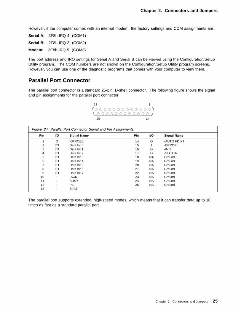
Parallel Port Connector
The parallel port connector is a standard 25-pin, D-shell connector. The following figure shows the signaland pin assignments for the parallel port connector.
13 1
25 14
The parallel port supports extended, high-speed modes, which means that it can transfer data up to 10times as fast as a standard parallel port.
Figure 24. Parallel Port Connector Signal and Pin Assignments
Pin I/O Signal Name Pin I/O Signal Name
1 O -STROBE 14 O -AUTO FD XT2 I/O Data bit 0 15 I -ERROR3 I/O Data bit 1 16 O -INIT4 I/O Data bit 2 17 O -SLCT IN5 I/O Data bit 3 18 NA Ground6 I/O Data bit 4 19 NA Ground7 I/O Data bit 5 20 NA Ground8 I/O Data bit 6 21 NA Ground9 I/O Data bit 7 22 NA Ground
10 I -ACK 23 NA Ground11 I BUSY 24 NA Ground12 I PE 25 NA Ground13 I SLCT
Chapter 2. Connectors and Jumpers 25

Chapter 2. Connectors and Jumpers
Parallel-Port Setup
Each parallel connector or adapter in your computer can use any of three available port settings, providedthat a different setting is used for each. The settings include the port address (in hexadecimal) and theinterrupt request line (IRQ), which determines how the microprocessor responds to an interrupt from theparallel port. The three available port settings, in sequential order, are:
3BCh-IRQ 5 or 7378h-IRQ 5 or 7278h-IRQ 5 or 7
There is no direct relationship among the three available port settings and the three LPT numbers. Whenyou start the computer, POST (power-on self test) assigns LPT numbers to the port addresses that areactually in use at the time. POST goes down the list of addresses sequentially to assign LPT numbers toeach address in use by a parallel device. If an address is not in use, an LPT number is not assigned to it.POST assigns the next available LPT number to the next address in use. The port address and IRQsetting for the built-in parallel port are preset at the factory, as follows:
Built-in port: 3BCh-IRQ 7
POST assigns an LPT number to the built-in parallel port during startup, as follows:
Built-in port: 3BCh-IRQ 7 (LPT1)
If you add another parallel adapter that uses the next sequential address, POST assigns LPT numbers asfollows:
Built-in port: 3BCh-IRQ 7 (LPT1)
Adapter port: 378h-IRQ 5 (LPT2)
The port address and IRQ settings for the built-in parallel port can be viewed using theConfiguration/Setup Utility program. The LPT number is not shown on the Configuration/Setup Utilityprogram screens. However, you can use one of the diagnostic programs that comes with your computerto view it.
The parallel-port setting must be changed if you use ECP, EPP, or ECP/EPP modes because 3BCh-IRQ 7cannot be used for these modes. The setting can be changed using the Configuration/Setup Utilityprogram.
26 Technical Information Manual
Chapter 2. Connectors and Jumpers
Parallel-Port Modes
The parallel port can operate in five different modes. One is a standard, unidirectional mode; the otherfour are extended, bidirectional modes that provide additional function and higher performance. Refer tothe documentation that comes with your printer or other parallel device to determine the appropriateparallel mode to use and to get information on the required device drivers.
Standard This AT-compatible mode is the default mode. In this mode, the parallel port islimited to writing information to the device attached to it. This mode can be usedwith most IBM-compatible parallel printers.
Bidirectional This PS/2-compatible mode is a bidirectional mode used for data transfer to otherPC systems and supported devices.
ECP The extended capabilities port (ECP) mode is a high-performance, bidirectionalmode that uses direct memory access (DMA) for data transfer to a high-speedprinter or to other devices.
EPP The enhanced parallel port (EPP) mode is a high-performance, bidirectional modethat has capabilities similar to the ECP mode. The main difference between the twomodes is that EPP data transfers are processor-initiated instead of DMA-initiated.EPP supports the connection of up to eight external devices such as hard diskdrives, CD-ROM drives, tape drives, diskette drives, and a printer to the parallelport. These devices can be connected to each other in a daisy-chain arrangement,or they can be connected through an external multiplexor. The attachment ofmultiple devices requires device drivers supplied by the device manufacturers.
ECP/EPP This mode combines the capabilities of the ECP and EPP modes. Select this modeto connect both ECP and EPP devices to the parallel port.
To select the mode of operation for the parallel port, use the Configuration/Setup Utility program.
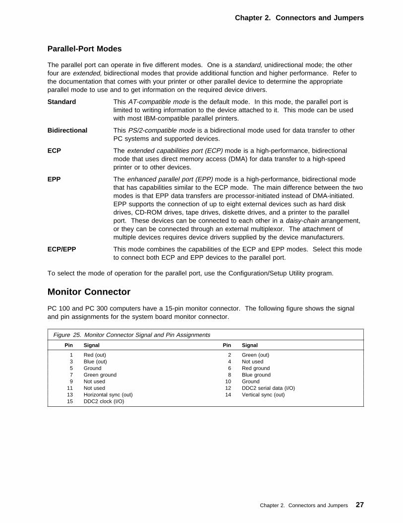
Monitor Connector
PC 100 and PC 300 computers have a 15-pin monitor connector. The following figure shows the signaland pin assignments for the system board monitor connector.
Figure 25. Monitor Connector Signal and Pin Assignments
Pin Signal Pin Signal
1 Red (out) 2 Green (out)3 Blue (out) 4 Not used5 Ground 6 Red ground7 Green ground 8 Blue ground9 Not used 10 Ground
11 Not used 12 DDC2 serial data (I/O)13 Horizontal sync (out) 14 Vertical sync (out)15 DDC2 clock (I/O)
Chapter 2. Connectors and Jumpers 27
Chapter 3. Memory Subsystems
Chapter 3. Memory Subsystems
Memory-Module Description . . . . . . . . . . . . . . . . . . . . . . . . . . . . . . . . . . . . . . . . . . . 29Memory-Module Configurations . . . . . . . . . . . . . . . . . . . . . . . . . . . . . . . . . . . . . . . . . . 29Cache Memory . . . . . . . . . . . . . . . . . . . . . . . . . . . . . . . . . . . . . . . . . . . . . . . . . . . 30
Cache Upgrade Options . . . . . . . . . . . . . . . . . . . . . . . . . . . . . . . . . . . . . . . . . . . . 30
28 Copyright IBM Corp. August 1996

Chapter 3. Memory Subsystems
Memory-Module Description
PC 100 and PC 300 computers have four SIMM connectors. After memory modules are installed, thePlug and Play feature of the BIOS automatically detects the additional memory modules.
Notes:
1. Memory modules can have a maximum height of 1.2 inches.2. Parity checking is not supported.3. A mix of parity and non-parity SIMMs will be configured as non-parity.4. A mix of extended-data output (EDO) and fast page (FP) SIMMs can be installed in the PC 300 if
matched pairs are installed in each bank.
Memory-Module Configurations
The following tables show the typical memory-module configurations for the PC 100 and PC 300.
Figure 26. Memory-Module Type, Speed, and Size – PC 100
Type Speed Memory-Module Size
Fast page 70 ns 4 MB, 8 MB, 16 MB, 32 MB
Figure 27. Memory-Module Type, Speed, and Size – PC 300
Type Speed Memory-Module Size
EDO (preinstalled) 60 ns 4 MB, 8 MB, 16 MB, 32 MBFast page (supported) 70 ns 4 MB, 8 MB, 16 MB, 32 MB
Figure 28. System Memory Table
TotalMemory
Bank 0SIMM 1, 2
Bank 1SIMM 3, 4
4 MBñ 4, 0 0, 0
8 MB 4, 4 0, 0
16 MB 0, 0 8, 8
16 MB 4, 4 4, 4
24 MB 8, 8 4, 4
24 MB 4, 4 8, 8
32 MB 8, 8 0, 0
32 MB 0, 0 8, 8
40 MB 4, 4 16, 16
40 MB 16, 16 4, 4
48 MB 8, 8 16, 16
64 MB 16, 16 16, 16
64 MB 32, 32 0, 0
72 MB 4, 4 32, 32
80 MB 8, 8 32, 32
96 MB 16, 16 32, 32
128 MB 32, 32 32, 32
ñ A 4 MB, single SIMM is supported by the PC 100 only.
Chapter 3. Memory Subsystems 29
Chapter 3. Memory Subsystems
Cache Memory
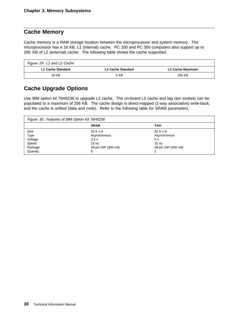
Cache memory is a RAM storage location between the microprocessor and system memory. Themicroprocessor has a 16 KB, L1 (internal) cache. PC 100 and PC 300 computers also support up to256 KB of L2 (external) cache. The following table shows the cache supported.
Cache Upgrade Options
Use IBM option kit 76H0236 to upgrade L2 cache. The on-board L2 cache and tag ram sockets can bepopulated to a maximum of 256 KB. The cache design is direct-mapped (1-way associative) write-back,and the cache is unified (data and code). Refer to the following table for SRAM parameters.
Figure 29. L1 and L2 Cache
L1 Cache Standard L2 Cache Standard L2 Cache Maximum
16 KB 0 KB 256 KB
Figure 30. Features of IBM Option Kit 76H0236
SRAM TAG
Size 32 K x 8 32 K x 8Type Asynchronous AsynchronousVoltage 3.3 v 5 vSpeed 15 ns 15 nsPackage 28-pin DIP (300 mil) 28-pin DIP (300 mil)Quantity 8 1
30 Technical Information Manual
Chapter 4. System Compatibility
Chapter 4. System Compatibility
Hardware Compatibility . . . . . . . . . . . . . . . . . . . . . . . . . . . . . . . . . . . . . . . . . . . . . . 32Hardware Interrupts . . . . . . . . . . . . . . . . . . . . . . . . . . . . . . . . . . . . . . . . . . . . . . . 32Diskette Drives and Controller . . . . . . . . . . . . . . . . . . . . . . . . . . . . . . . . . . . . . . . . . 33Hard Disk Drives and Controller . . . . . . . . . . . . . . . . . . . . . . . . . . . . . . . . . . . . . . . . 34
Software Compatibility . . . . . . . . . . . . . . . . . . . . . . . . . . . . . . . . . . . . . . . . . . . . . . . 34Software Interrupts . . . . . . . . . . . . . . . . . . . . . . . . . . . . . . . . . . . . . . . . . . . . . . . 34Machine-Sensitive Programs . . . . . . . . . . . . . . . . . . . . . . . . . . . . . . . . . . . . . . . . . 34
BIOS Compatibility . . . . . . . . . . . . . . . . . . . . . . . . . . . . . . . . . . . . . . . . . . . . . . . . . 35
Copyright IBM Corp. August 1996 31
Chapter 4. System Compatibility
Hardware Compatibility
This section briefly discusses hardware, software, and BIOS compatibility issues that must be consideredwhen designing application programs.
Many of the interfaces are the same as those used by the IBM Personal Computer AT. In most cases,the command and status organization of these interfaces is maintained.
The functional interfaces are compatible with the following interfaces:
� The Intel 8259 interrupt controllers (edge-triggered mode).
� The National Semiconductor NS16450 and NS16550A serial communication controllers.
� The Motorola MC146818 Time of Day Clock command and status (CMOS reorganized).
� The Intel 8254 timer, driven from a 1.193 MHz clock (channels 0, 1, and 2).
� The Intel 8237 DMA controller, except for the Command and Request registers and the Rotate andMask functions. The Mode register is partially supported.
� The Intel 8272 or 82077 diskette drive controllers.
� The Intel 8042 keyboard controller at addresses 0060h and 0064h.
� All video standards using VGA, EGA, CGA, MDA, and Hercules modes.
� The parallel printer ports (Parallel 1, Parallel 2, and Parallel 3) in compatibility mode.
Use the following information to develop application programs for personal computer products. Wheneverpossible, use the BIOS as an interface to hardware to provide maximum compatibility and portability ofapplications among systems.
Hardware Interrupts
Hardware interrupts are level sensitive for PCI interrupts and edge sensitive for ISA interrupts. Theinterrupt controller clears its in-service register bit when the interrupt routine sends an End-of-Interrupt(EOI) command to the controller. The EOI command is sent regardless of whether the incoming interruptrequest to the controller is active or inactive.
The interrupt-in-progress latch is readable at an I/O-address bit position. This latch is read during theinterrupt service routine and might be reset by the read operation, or it might require an explicit reset.
Note: For performance and latency considerations, designers might want to limit the number of devicessharing an interrupt level.
With level-sensitive interrupts, the interrupt controller requires that the interrupt request be inactive at thetime the EOI command is sent; otherwise, a new interrupt request will be detected. To avoid this, alevel-sensitive interrupt handler must clear the interrupt condition (usually by a read or write operation toan I/O port on the device causing the interrupt). After processing the interrupt, the interrupt handler:
1. Clears the interrupt
2. Waits one I/O delay
3. Sends the EOI
4. Waits one I/O delay
5. Enables the interrupt through the Set Interrupt Enable Flag command
32 Technical Information Manual

Chapter 4. System Compatibility
Hardware interrupt IRQ9 is defined as the replacement interrupt level for the cascade level IRQ2.Program interrupt sharing is implemented on IRQ2, interrupt 0Ah. The following processing occurs tomaintain compatibility with the IRQ2 used by IBM Personal Computer products:
1. A device drives the interrupt request active on IRQ2 of the channel.
2. This interrupt request is mapped in hardware to IRQ9 input on the second interrupt controller.
3. When the interrupt occurs, the system microprocessor passes control to the IRQ9 (interrupt 71h)interrupt handler.
4. This interrupt handler performs an EOI command to the second interrupt controller and passes controlto the IRQ2 (interrupt 0Ah) interrupt handler.
5. This IRQ2 interrupt handler, when handling the interrupt, causes the device to reset the interruptrequest before performing an EOI command to the master interrupt controller that finishes servicingthe IRQ2 request.
Diskette Drives and Controller
The following figures show the reading, writing, and formatting capabilities of each type of diskette drive.
Notes:
1. Do not use 5.25-inch diskettes that are designed for the 1.2 MB mode in either a 160/180 KB or320/360 KB diskette drive.
2. Low-density 5.25-inch diskettes that are written to or formatted by a high-capacity 1.2 MB diskettedrive can be reliably read only by another 1.2 MB diskette drive.
3. Do not use 3.5-inch diskettes that are designed for the 2.88 MB mode in a 1.44 MB diskette drive.
Figure 31. 5.25-Inch Diskette Drive Reading, Writing, and Formatting Capabilities
Diskette Drive Type160/180 KB
Mode320/360 KB
Mode1.2 MBMode
5.25-inch diskette drive: Single sided (48 TPI) RWF — —Double sided (48 TPI) RWF RWF —High capacity (1.2 MB) RWF RWF RWF
R = Read W = Write F = Format
Figure 32. 3.5-Inch Diskette Drive Reading, Writing, and Formatting Capabilities
Diskette Drive Type 720 KB Mode 1.44 MB Mode
3.5-inch diskette drive:1.44 MB drive RWF RWF
R = Read W = Write F = Format
Chapter 4. System Compatibility 33
Chapter 4. System Compatibility
Copy Protection
The following methods of copy protection might not work in systems using a 3.5-inch, 1.44 MB diskettedrive.
� Bypassing BIOS routines:
– Data transfer rate: BIOS selects the proper data transfer rate for the media being used.
– Diskette parameter table: Copy protection, which creates its own diskette parameter table, mightnot work in these drives.
� Diskette drive controls:
– Rotational speed: The time between two events in a diskette drive is a function of the controller.
– Access time: Diskette BIOS routines must set the track-to-track access time for the different typesof media that are used in the drives.
– ‘Diskette change’ signal: Copy protection might not be able to reset this signal.
� Write-current control: Copy protection that uses write-current control does not work, because thecontroller selects the proper write current for the media that is being used.
Hard Disk Drives and Controller
Reading from and writing to the hard disk is initiated in the same way as in other IBM Personal Computerproducts; however, some new functions are supported.
Software Compatibility
To maintain software compatibility, the interrupt polling mechanism that is used by IBM Personal Computerproducts is retained. Software that interfaces with the reset port for the IBM Personal Computerpositive-edge interrupt sharing (hex address 02Fx or 06Fx, where x is the interrupt level) does not createinterference.
Software Interrupts
With the advent of software interrupt sharing, software interrupt routines must daisy chain interrupts. Eachroutine must check the function value, and if it is not in the range of function calls for that routine, it musttransfer control to the next routine in the chain. Because software interrupts are initially pointed toaddress 0:0 before daisy chaining, check for this case. If the next routine is pointed to address 0:0 andthe function call is out of range, the appropriate action is to set the carry flag and do a RET 2 to indicatean error condition.
Machine-Sensitive Programs
Programs can select machine-specific features, but they must first identify the machine and model type.IBM has defined methods for uniquely determining the specific machine type. The machine model bytecan be found through Interrupt 15H, Return System Configuration Parameters function ((AH)=C0H). Seethe IBM Personal System/2 and Personal Computer BIOS Interface Technical Reference for a listing ofmodel bytes for other IBM Personal Computer products.
34 Technical Information Manual

Chapter 4. System Compatibility
BIOS Compatibility
PC 100 computers support the following industry standard BIOS interfaces:
Advanced Power Management (APM) Version 1.2
Plug and Play (PnP) Version 1.0A
Desktop Management Interface (DMI) Version 2.0
PC 300 computers support the following industry standard BIOS interfaces:
Advanced Power Management (APM) Version 1.2
Plug and Play (PnP) Version 1.0A
For additional information on BIOS interfaces supported, refer to the IBM Personal System/2 and PersonalComputer BIOS Interface Technical Reference.
Chapter 4. System Compatibility 35
Chapter 5. Bus Architecture
Chapter 5. Bus Architecture
Bus Architecture Descriptions . . . . . . . . . . . . . . . . . . . . . . . . . . . . . . . . . . . . . . . . . . . 37ISA Bus . . . . . . . . . . . . . . . . . . . . . . . . . . . . . . . . . . . . . . . . . . . . . . . . . . . . . . 37PCI Bus . . . . . . . . . . . . . . . . . . . . . . . . . . . . . . . . . . . . . . . . . . . . . . . . . . . . . . 38
PCI Performance . . . . . . . . . . . . . . . . . . . . . . . . . . . . . . . . . . . . . . . . . . . . . . . 38PCI Peripheral Devices . . . . . . . . . . . . . . . . . . . . . . . . . . . . . . . . . . . . . . . . . . . 38
Expansion-Bus Features . . . . . . . . . . . . . . . . . . . . . . . . . . . . . . . . . . . . . . . . . . . . 38Bus Voltage Levels . . . . . . . . . . . . . . . . . . . . . . . . . . . . . . . . . . . . . . . . . . . . . . . 39
36 Copyright IBM Corp. August 1996

Chapter 5. Bus Architecture
Bus Architecture Descriptions
This section gives an overview of input/output (I/O) buses and explains how advanced I/O buses canimprove performance.
A computer bus is a pathway of wires and signals that carry (or transfer) information inside the computer.Information includes data, addresses, instructions, and controls. The microprocessor has an external bus,called the microprocessor bus or local bus, that carries information between the microprocessor and mainmemory. The local bus has the same bus width (64 bits) as the microprocessor and operates at the sameexternal speed.
Another computer bus, the I/O bus or expansion bus, carries information between the microprocessor ormemory and the I/O (peripheral) devices. While microprocessor-bus performance has improved rapidly,improvements in I/O-bus performance have not equalled those of microprocessors and some peripheraldevices, such as video and disk controllers. Regardless of how fast the microprocessor and othercomponents are, data transfers between them must pass through the I/O bus.
The computer has two I/O buses: the ISA bus and the PCI bus. ISA has been the standard I/O bus usedin IBM and IBM-compatible computers for many years. PCI is one of the advanced I/O bus standardsdeveloped by the computer industry to keep up with performance improvements of microprocessor busesand advanced peripheral devices. Although advanced designs, such as PCI, cannot match theperformance of the microprocessor bus, they do achieve higher throughput by speeding up the I/O busand widening its data path. PCI is intended to add to, but not replace, the capability of the ISA bus. Infact, most personal computers today need only three PCI connections: one for video, one for the diskcontroller, and one for a network adapter or other optional device.
ISA Bus
One of the most widely used and successful bus architectures is the AT bus, also called the industrystandard architecture (ISA) bus, or the I/O channel. The ISA bus is a 16-bit bus that operates at a speedof 8 MHz. It can transfer up to 8 MB of data per second between the microprocessor and an I/O device.Practical performance ranges between 4 MB to 8 MB per second.
The ISA bus continues to be popular because so many adapters, devices, and applications have beendesigned and marketed for it. ISA is adequate for users of DOS applications in a stand-aloneenvironment, or for DOS network requestors with moderate performance requirements.
Although the ISA bus is widely used and is suitable for many applications, it cannot transfer data fastenough for today's high-speed microprocessors and I/O devices. For example, the ISA bus might notprovide for the performance needs of video devices and applications with high-resolution and high-colorcontent. Also, ISA might not be capable of handling the throughput required by some fast hard diskdrives, network controllers, or full-motion video adapters.
In PC 100 and PC 300 computers, the ISA bus is buffered to provide sufficient power for the 98-pinconnectors, assuming two low-power Schottky (LS) loads per slot. The signal assignments and pinassignments for the I/O channel connectors are shown in Figure 15 on page 18.
Chapter 5. Bus Architecture 37

Chapter 5. Bus Architecture
PCI Bus
The PCI bus connects to the microprocessor local bus through a buffered bridge controller. A bridgetranslates signals from one bus architecture to another. PCI and ISA devices receive all their data andcontrol information through the PCI controller. The PCI controller looks at all signals from themicroprocessor local bus and then passes them to the ISA controller, or to peripheral devices connectedto the PCI bus. However, the PCI bus is not governed by the speed of the microprocessor bus. PCI canoperate at speeds as fast as 33 MHz, slow down, or even stop if there is no activity on the bus, allindependent of the microprocessor’s operations. This independence is a distinguishing feature of PCI thatallows the microprocessor to do other work while the I/O bus is busy. Microprocessor independence alsomakes PCI adaptable to various microprocessor speeds and families and allows consistency in the designand use of PCI peripheral devices across multiple computer families.
PCI Performance
One of the most significant features of PCI is its 32-bit data path, which is twice the width of the ISA datapath. With a 32-bit data path, the PCI bus can transfer more information per second than the ISA buswith its 16-bit data path. Also, PCI operates at higher speeds of up to 33 MHz. Depending on the modeof operation and computer components used, the PCI bus can transfer data at speeds up to 132 MB persecond. While many factors can reduce practical performance, achieving just half or a third of the PCImaximum theoretical throughput far exceeds the practical performance of the ISA bus at 4 MB to 8 MBper second.
PCI Peripheral Devices
The wider data path and higher throughput make PCI a more suitable bus for today's high-speedmicroprocessors and I/O devices. Higher throughput translates into higher performance of peripheraldevices, such as higher video resolutions, more colors, and quicker screen refreshes. The use of PCIarchitecture enhances the performance of the monitor and the storage devices. Both the video controllerand the EIDE drive controller are connected to the PCI bus on the system board. Thus, the peripheraldevices that have the greatest demand for high performance are supported by the benefits of PCIarchitecture.
Expansion-Bus Features
The bit-width of the I/O bus determines the type of adapters the computer supports. The shared slotshandle 16-bit, ISA adapters and 32-bit, PCI adapters. The dedicated ISA slots handle 16-bit, ISA adaptersonly. The width of the I/O bus does not affect software compatibility.
The PC 100 and PC 300 riser card has one shared PCI and ISA slot, one dedicated PCI slot, and twodedicated ISA slots to support a maximum of four adapters at a given time.
(On other side)PCI(SharedSlot 3)
ISA(SharedSlot 3)
(On other side)
PCI(Slot 4)
Riser Card
ISA(Slot 2)
ISA(Slot 1)
3.3 Volt PCIConnector
38 Technical Information Manual

Chapter 5. Bus Architecture
One ISA connector and the PCI connector directly below it share an expansion-slot opening at the back ofthe computer that can be used by only one adapter at a time. This means that you can install either aPCI adapter or an ISA adapter in a shared slot, but not both.
PCI devices receive data through the PCI controller. The PCI controller looks at all signals from themicroprocessor local bus, then passes them to the ISA controller or to peripherals connected to the PCIbus.
The signal assignments and pin assignments for the PCI connectors are shown in Figure 16 on page 19.For additional information, see the PCI Local Bus Specification, published by the PCI Special InterestGroup.
Bus Voltage LevelsFour voltage levels are provided for I/O adapters. The maximum available values (for each slot) are asfollows:
� +5 V dc (+5%, −4.5%) at 2.0 A� −5 V dc (+10%, −9.5%) at 0.100 A� +12 V dc (+5%, −4.5%) at 0.175 A� −12 V dc (+10%, −9.5%) at 0.100 A
The I/O CH RDY signal is available on the I/O channel to allow operation with slow I/O or memory devices.I/O CH RDY is held inactive by an addressed device to lengthen the operation. For each clock cycle thatthe line is held inactive, one wait state is added to the I/O or DMA operation.
One voltage level is provided for PCI bus adapters. The maximum available values for each slot are +5 Vdc (+5%, −4.5%) at 7.576 A.
Chapter 5. Bus Architecture 39

Appendix A. Error Codes
Appendix A. Error Codes
This section identifies the POST error codes and beep error codes for the PC 100 and PC 300.
POST Error Codes
POST error messages appear when POST finds problems with the hardware during startup, or when achange in the hardware configuration is found. POST error messages are 3-, 4-, 5-, 8-, or 12-characteralphanumeric messages. An x in an error message can represent any number.
Figure 33 (Page 1 of 2). POST Error Messages – PC 100 and PC 300
Code Description
101 Interrupt failure102 Timer failure103 Timer-interrupt failure104 Protected mode failure105 Last 8042 command not accepted – keyboard failure106 System board failure108 Timer bus failure109 Low MB chip select test110 System board parity error 1 (system board parity latch set)111 I/O parity error 2 (I/O channel check latch set)112 I/O channel check error113 I/O channel check error114 External ROM checksum error115 DMA error116 System board port read/write error120 Microprocessor test error121 Hardware error151 Real time clock failure161 Bad CMOS battery162 CMOS RAM checksum/configuration error163 Clock not updating164 CMOS RAM memory size does not match167 Clock not updating175 Riser card or system board error176 System cover has been removed177 Corrupted administrator password178 Riser card or system board error183 Administrator password has been set and must be entered184 Password removed due to checksum error185 Corrupted boot sequence186 System board or hardware security error189 More than three password attempts were made to access system201 Memory date error202 Memory address line error 00-15203 Memory address line error 16-23221 ROM to RAM remapping error225 Unsupported memory type installed or memory pair mismatch301 Keyboard error302 Keyboard error303 Keyboard to system board interface error304 Keyboard clock high305 No keyboard +5 V601 Diskette drive or controller error602 Diskette IPL boot record not valid604 Unsupported diskette drive installed605 POST cannot unlock diskette drive662 Diskette drive configuration error762 Math coprocessor configuration error
40 Copyright IBM Corp. August 1996
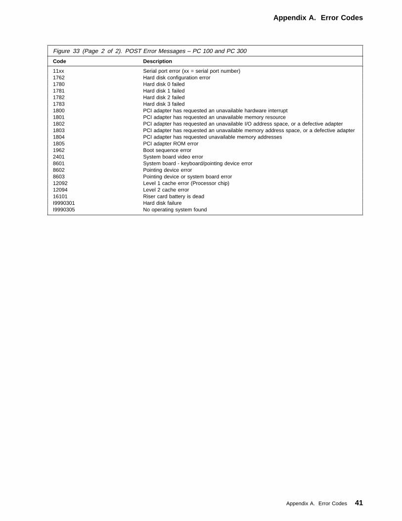
Appendix A. Error Codes
Figure 33 (Page 2 of 2). POST Error Messages – PC 100 and PC 300
Code Description
11xx Serial port error (xx = serial port number)1762 Hard disk configuration error1780 Hard disk 0 failed1781 Hard disk 1 failed1782 Hard disk 2 failed1783 Hard disk 3 failed1800 PCI adapter has requested an unavailable hardware interrupt1801 PCI adapter has requested an unavailable memory resource1802 PCI adapter has requested an unavailable I/O address space, or a defective adapter1803 PCI adapter has requested an unavailable memory address space, or a defective adapter1804 PCI adapter has requested unavailable memory addresses1805 PCI adapter ROM error1962 Boot sequence error2401 System board video error8601 System board - keyboard/pointing device error8602 Pointing device error8603 Pointing device or system board error12092 Level 1 cache error (Processor chip)12094 Level 2 cache error16101 Riser card battery is deadI9990301 Hard disk failureI9990305 No operating system found
Appendix A. Error Codes 41
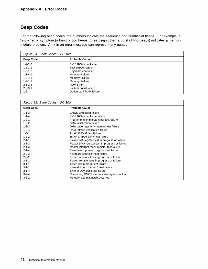
Appendix A. Error Codes
Beep Codes
For the following beep codes, the numbers indicate the sequence and number of beeps. For example, a“2-3-2” error symptom (a burst of two beeps, three beeps, then a burst of two beeps) indicates a memorymodule problem. An x in an error message can represent any number.
Figure 34. Beep Codes – PC 100
Beep Code Probable Cause
1-2-2-3 BIOS ROM checksum1-3-1-1 Test DRAM refresh1-3-1-3 Keyboard controller1-3-4-1 Memory Failure1-3-4-3 Memory Failure1-4-1-1 Memory Failure2-1-2-3 ROM error2-2-3-1 System board failure1-2 Option card ROM failure
Figure 35. Beep Codes – PC 300
Beep Code Probable Cause
1-1-3 CMOS write/read failure1-1-4 BIOS ROM checksum failure1-2-1 Programmable interval timer test failure1-2-2 DMA initialization failure1-2-3 DMA page register write/read test failure1-2-4 RAM refresh verification failure1-3-1 1st 64 K RAM test failure1-3-2 1st 64 K RAM parity test failure2-1-1 Slave DMA register test in progress or failure2-1-2 Master DMA register test in progress or failure2-1-3 Master interrupt mask register test failure2-1-4 Slave interrupt mask register test failure2-2-2 Keyboard controller test failure2-3-2 Screen memory test in progress or failure2-3-3 Screen retrace tests in progress or failure3-1-1 Timer tick interrupt test failure3-1-2 Interval timer channel 2 test failure3-1-4 Time-of-Day clock test failure3-2-4 Comparing CMOS memory size against actual3-3-1 Memory size mismatch occurred
42 Technical Information Manual

Appendix D. Notices and Trademarks
Appendix B. Notices and Trademarks
References in this publication to IBM products, programs, or services do not imply that IBM intends tomake these available in all countries in which IBM operates. Any reference to an IBM product, program,or service is not intended to state or imply that only that IBM product, program, or service may be used.Subject to IBM’s valid intellectual property or other legally protectable rights, any functionally equivalentproduct, program, or service may be used instead of the IBM product, program, or service. The evaluationand verification of operation in conjunction with other products, except those expressly designated by IBM,are the responsibility of the user.
IBM may have patents or pending patent applications covering subject matter in this document. Thefurnishing of this document does not give you any license to these patents. You can send licenseinquiries, in writing, to:
IBM Director of Licensing IBM Corporation
500 Columbus Avenue Thornwood, NY 10594 U.S.A.
Copyright IBM Corp. August 1996 43

Appendix D. Notices and Trademarks
Trademarks
The following terms are trademarks of the IBM Corporation in the United States or other countries or both:
The following terms are trademarks of other companies:
Microsoft, Windows, and Windows NT, are trademarks or registered trademarks of Microsoft Corporation.
Other company, product, and service names, which may be denoted by a double asterisk (**), may betrademarks or service marks of others.
AT Personal System/2PC 100 PS/2PC 300 XTPersonal Computer AT
1-2-3 Lotus Development CorporationCA Computer AssociatesCirrus Cirrus Logic, Inc.Cirrus Logic Cirrus Logic, Inc.DMI Desktop Management Task ForceHercules Hercules Computer TechnologyIntel Intel CorporationLotus Lotus Development CorporationMotorola Motorola, Inc.National Semiconductor National Semiconductor Corp.Pentium Intel CorporationSMC Standard Microsystems CorporationVESA Video Electronics Standards Association
44 Technical Information Manual

References
� ANSI ATA-2 (AT Attachment)Source: American National Standards Institute,New York, NY
� CL-GD54xx Alpine VGA FamilySource: Cirrus Logic, Freemont, CA
� Extended Capabilities Port: Specification KitSource: Microsoft Corporation, Redmond, WA
� Intel Microprocessor and Peripheral ComponentLiteratureSource: Intel Corporation, Santa Clara, CA
� PCI Local Bus SpecificationSource: PCI Special Interest Group, Hillsboro, OR
� Personal System/2 and Personal Computer BIOSInterface Technical ReferenceSource: IBM
� Personal System/2 ATA/IDE Fixed Disk DrivesTechnical ReferenceSource: IBM
� Personal System/2 Hardware Interface TechnicalReference – ArchitecturesSource: IBM
� Personal System/2 Hardware Interface TechnicalReference – Common InterfacesSource: IBM
� SiS5511/2/3 Shared MemorySource: Silicon Integrated Systems Corporation,Sunnyvale, CA
Copyright IBM Corp. August 1996 45
index
Index
Numerics16550-UART 24
Aadapters, adding 38address maps, system 7advanced power management 14, 35altitude 13APM 14, 35AT bus 37AT-compatible mode (parallel port) 27audio subsystem 4auxiliary device
and keyboard controller 5connector 23
Bbaud rate 24beep codes 42bidirectional mode (parallel port) 27BIOS
compatibility 35data areas 7
busarchitecture 4, 37AT 37ISA 37PCI 38
bypassing BIOS 34
Ccables 13cache memory
external 4, 30internal 30upgrade options 30
CMOS RAM 4compatibility
BIOS 35hardware 32software 34
connectorauxiliary device 23CD-ROM 17diskette drive 16EIDE 17hard disk drive 17I/O 23ISA bus 18
connector (continued)keyboard 23memory 21monitor 27mouse 23parallel port 25PCI 19power supply 20serial port 24
controllerdiskette drive 5DMA 4hard disk drive 5interrupt 4keyboard/auxiliary device 5parallel port 5serial port 5
copy protection 34current, electrical 13
Ddepth, system unit 13description
AT bus 37auxiliary device connector 23diskette drive connector 16EIDE connectors 17hard disk drive connectors 17I/O channel 37ISA bus 37keyboard connector 23monitor connector 27mouse connector 23parallel port connector 25PCI connector 19power supply 11serial port connector 24system board memory connector 21
desktop management interface (DMI) 35diskette drive
capabilities 33change signal 34compatibility 34connector 16controller 5, 33signals 16write current 34
DMAchannel assignments 10controller 4I/O address map 9
46 Copyright IBM Corp. August 1996
index
EECP (extended capabilities port) 27ECP/EPP 27edge-triggered interrupts 32EIDE connectors 17electromagnetic compatibility 13enhanced parallel port (EPP) 27environment, operating 13EPP (enhanced parallel port) 27error codes
beep 42POST 40
expansion bus 37, 38extended capabilities port (ECP) 27
Ffault, overvoltage 12features 2flash ROM 4frequency
electrical 13input 11
Hhard disk drive
compatibility 34connectors 17controller 5, 34
hardwarecompatibility 32interrupts 32
heat output 13height, system unit 13humidity 13
II/O
address maps 7bus 37channel 37connectors 23DMA address map 9
input power requirements 11interrupt
controller 4request assignments 10
ISAconnectors 18controller 39expansion slots 38
ISA/PCI interface 4
Jjumper locations, system board 6
Kkeyboard
and auxiliary device controller 5cable 13connector 23
LL1 cache 30L2 cache 4, 30level-sensitive interrupts 32local bus 37
Mmachine-sensitive programs 34maps
I/O address 7memory address 7system address 7
measurements, system unit 13memory
cache 30connector 21error in 7L1 cache 30L2 cache 30maps, system 7RAM 7, 29SIMMs 29upgrade options 30
messages, POST error 40microprocessor 4modem 25modes, power management 14monitor connector 27mouse connector 23
Ooutput power parameters 11overview 2overvoltage fault 12
Pparallel port
connector 25feature 5
passwords 5PCI
connectors 19
Index 47

index
PCI (continued)controller 39expansion slots 38
Pentium microprocessor 4physical specifications 13plug and play (PnP) 35polling mechanism 34port
parallel 5, 25serial 5, 24
POST, errors 7, 40power
cable 13component output 12consumption 14input requirements 11management modes 14output parameters 11output protection 12specifications 13supply 5, 11, 20
protection, power supply 12PS/2-compatible mode (parallel port) 27publications, related vi
RRAM (random access memory) 4, 7, 29random access memory (RAM) 4, 7, 29references 45registers virelated publications vireserved areas viriser card 38
Ssecurity, system 5serial port
connector 24feature 5
short circuit 12signals
diskette drive 16hard disk drive 17representation of vi
SIMMs (single inline memory modules) 29single inline memory modules (SIMMs) 29size, system unit 13software
compatibility 34interrupts 34
specifications, physical 13standard mode (parallel port) 27system
description 2
system (continued)memory maps 7specifications 13timers 4
system boardauxiliary device connector 23devices 4diagram 6diskette drive connector 16EIDE connectors 17features 4hard disk drive connectors 17jumper locations 6keyboard connector 23memory connector 21monitor connector 27mouse connector 23parallel port connector 25PCI connector 19power supply connectors 20serial port connector 24video feature connector 22
Ttemperature 13timers, system 4
UUART (universal asynchronous receiver/transmitter) 24unidirectional mode (parallel port) 27universal asynchronous receiver/transmitter (UART) 24
Vvideo
feature connector 22subsystem 4
voltage, input 11
Wweight, system unit 13width, system unit 13write current, diskette 34
48 Technical Information Manual


IBM
Part Number: 78H5142
Printed in U.S.A.
78H5142
S78H-5142-ðð