Technical Guide - Diagramasde.comdiagramasde.com/diagramas/otros2/TH-42PD50U.pdf · BBE, the BBE...
85
Technical Guide Plasma Training Course TH-37PX50U, TH-42PD50U, TH-42PX50U, TH-42PX500U, TH-50PX50U, TH-50PX500U GP8DU and GPH8DU Chassis Troubleshooting Panasonic Services Company National Training
Transcript of Technical Guide - Diagramasde.comdiagramasde.com/diagramas/otros2/TH-42PD50U.pdf · BBE, the BBE...

Technical Guide Plasma Training Course
TH-37PX50U, TH-42PD50U, TH-42PX50U,
TH-42PX500U, TH-50PX50U, TH-50PX500U GP8DU and GPH8DU Chassis
Troubleshooting
Panasonic Services Company
National Training

Jean Mag Panason
N
"HDMI, the HDMI logo and High-Definition Multimedia InBBE, the BBE logo, Sonic Maximizer and High Definitio
Copyright © 2005 by Panasonic Services Company All rights reserved. Unauthorized copying and distributi
This service information is designed for expethe general public. It does not contain warnidangers in attempting to service a product. Ponly by experienced professional techniciandealt with in this service information by anyo
Prepared by loire & Cesar Perdomoic Services Company ational Training
terface are trademarks or registered trademarks of HDMI Licensing LLC." n Sound are registered trademarks or trademarks of BBE Sound, Inc.
on is a violation of law.
Warning rienced repair technicians only and is not designed for use by
ngs or cautions to advise non-technical individuals of potentialroducts powered by electricity should be serviced or repaireds. Any attempt to service or repair the product or products
ne else could result in serious injury or death.

Table of Contents Objective ........................................................................................................................ 1
Specifications (Models Comparison) .......................................................................... 2
Safety Precautions........................................................................................................ 3
TH-42PD50U Board Description and Part Numbers................................................... 4
TH-42PX500U Board Description and Part Numbers ................................................. 5
TH-50PX500 Board Description and Part Numbers.................................................... 6
Power Supply Outline for 42”and 50” Models ............................................................ 7 Standby Circuit......................................................................................................... 8 Power On Operation .............................................................................................. 12
Power Supply Connections........................................................................................ 15 P Board .................................................................................................................. 15 PA Board................................................................................................................ 16 PB Board................................................................................................................ 17
TH-42PX500U Block Diagram..................................................................................... 18
TH-42PX50U Block Diagram....................................................................................... 21
TH-42PD50U Block Diagram....................................................................................... 23
Video Input Selection Block Diagram........................................................................ 25
Audio Input Selection Block Diagram ....................................................................... 26
ATSC, SD and PC Card Input Signal Flow ................................................................ 27
DG Board Block Diagram ........................................................................................... 28
Signal Process Circuit ................................................................................................ 30 Main Picture Signal Flow........................................................................................ 30 Sub Picture Signal Flow ......................................................................................... 30 RGB Processor ...................................................................................................... 31
D Board Block Diagram .............................................................................................. 32
C1 Board Block Diagram ............................................................................................ 33
SC Board Explanation................................................................................................. 34 SC board Waveform............................................................................................... 35

SU And SD Board Shift Registers .......................................................................... 35
SS Board Explanation................................................................................................. 37 SS Board Schematic .............................................................................................. 38 SS Board Waveform .............................................................................................. 38
TH-42/50PX500U.......................................................................................................... 40
Power LED Flashing timing chart .............................................................................. 40
SOS Detection Circuits ............................................................................................... 41 SOS Detect (D Board)............................................................................................ 41 SOS Detect (DG Board)......................................................................................... 41 SOS Detect (D and PA Board) ............................................................................... 42
PA Board SOS Detection Circuits.............................................................................. 43 Over-Voltage Detection of Main Voltage (10 Blinks) .............................................. 43 Short Circuit Detection of Main Voltage (10 Blinks)................................................ 44 Short Circuit Detection of Sub-voltage (10 Blinks) ................................................. 45
Other SOS Detection Circuits .................................................................................... 46 SOS Detect (P, SC, and SS Board) ....................................................................... 46 P Board SOS Detection ......................................................................................... 47
Voltage Distribution of the PA board and SOS Detection ....................................... 48
Z Board (Sound) SOS Detection ............................................................................... 50
TH-42/50PX500U Self-check Function (Reset) .......................................................... 51 Diagnostic Procedures ........................................................................................... 51 How to access the Self-check Screen (Reset) ....................................................... 51 How to exit the Self-check Screen ......................................................................... 51
Screen Display......................................................................................................... 51
TH-42PD50U................................................................................................................. 53
Power LED Flashing timing chart .............................................................................. 53
TH-42/50PD50U Self-check Function......................................................................... 54 Diagnostic Procedures ........................................................................................... 54 How to access the Self-check Screen (Reset) ....................................................... 54 How to exit the Self-check Screen ......................................................................... 54
Screen Display......................................................................................................... 54
Serviceman Mode........................................................................................................ 56 How to enter the Serviceman Mode....................................................................... 56 Adjustment method ................................................................................................ 56 Cancellation ........................................................................................................... 56

Contents of adjustment mode ................................................................................ 56 Internal Pattern Generator ..................................................................................... 57
Cable Diagnostic Screen ............................................................................................ 57
Adjustments ................................................................................................................ 58 Driver Set-up.......................................................................................................... 58 Initialization Pulse Adjustment ............................................................................... 59
Drive Waveform ....................................................................................................... 59
P.C.B. (Printed Circuit Board) exchange procedure ................................................ 60
Adjustment Volume Locations................................................................................... 61
Test Point Locations................................................................................................... 62
Troubleshooting.......................................................................................................... 63 No Picture or Partial Picture................................................................................... 63 Scan and Sustain Drive Waveform ........................................................................ 66 Scan and Sustain Drive Check points .................................................................... 66 Vertical line problems............................................................................................. 71 Picture ok, Sound NG ............................................................................................ 72 No picture, no sound .............................................................................................. 73 No picture, sound ok .............................................................................................. 74 How to determine whether the D board or SC board is defective?......................... 75 Additional Troubleshooting Hints............................................................................ 76
SC20 or D20 Connector........................................................................................... 77 How to determine whether the D board or SS board is defective?......................... 78
Defective Board ....................................................................................................... 79
Glossary and Acronyms............................................................................................. 80

Objective This technical guide was prepared with the following objectives in mind: • Provide the servicer with a brief overview of the concepts of operation for new
circuits employed in this line of Plasma models • Provide drawings with emphasis on signal path to simplify the task of signal tracing
and locate the cause of a defect • Furnish troubleshooting procedures that contribute to a speedier repair of the
product • Provide examples of typical problems that may have occurred in similar types of
circuits
1
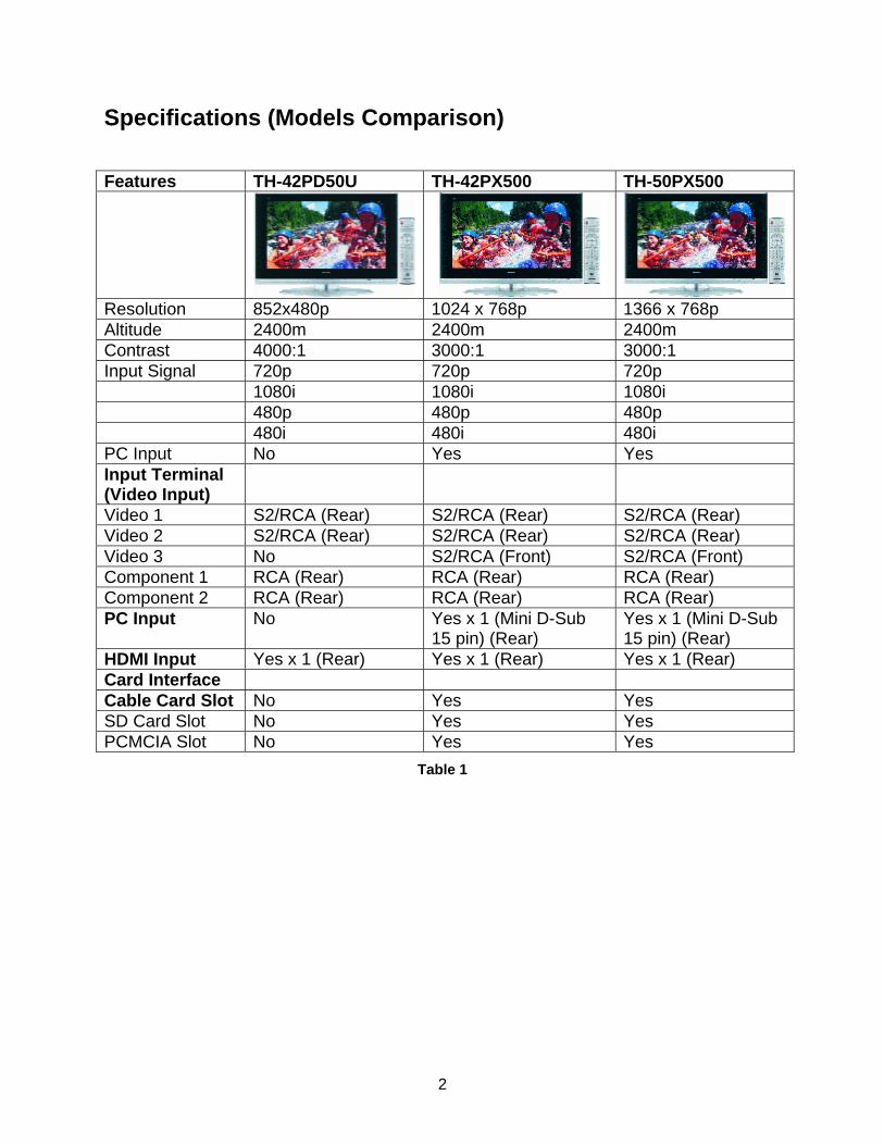
Specifications (Models Comparison) Features TH-42PD50U TH-42PX500 TH-50PX500
Resolution 852x480p 1024 x 768p 1366 x 768p Altitude 2400m 2400m 2400m Contrast 4000:1 3000:1 3000:1 Input Signal 720p 720p 720p 1080i 1080i 1080i 480p 480p 480p 480i 480i 480i PC Input No Yes Yes Input Terminal (Video Input)
Video 1 S2/RCA (Rear) S2/RCA (Rear) S2/RCA (Rear) Video 2 S2/RCA (Rear) S2/RCA (Rear) S2/RCA (Rear) Video 3 No S2/RCA (Front) S2/RCA (Front) Component 1 RCA (Rear) RCA (Rear) RCA (Rear) Component 2 RCA (Rear) RCA (Rear) RCA (Rear) PC Input No Yes x 1 (Mini D-Sub
15 pin) (Rear) Yes x 1 (Mini D-Sub 15 pin) (Rear)
HDMI Input Yes x 1 (Rear) Yes x 1 (Rear) Yes x 1 (Rear) Card Interface Cable Card Slot No Yes Yes SD Card Slot No Yes Yes PCMCIA Slot No Yes Yes
Table 1
2

Safety Precautions Please follow these general guidelines before servicing the models mentioned in this technical guide.
1. While servicing, please observe the original lead dress. If a short circuit is found, replace all the parts that have been overheated or damaged by the short circuit.
2. After servicing, please make sure that all the protective devices such as insulation barriers, and insulation paper shields are properly installed.
3. Some semiconductor (solid state) devices can be easily damaged by static electricity. Such components are commonly called Electrostatically Sensitive (ES) devices. Examples of typical ES devices are integrated circuits, some field-effect transistors (FET) and semiconductor "chip" components. The following techniques should be used to help reduce the incidence of component damage caused by Electro Static Discharge (ESD).
4. Drain off any Electro Static Discharge on your body by touching a known earth ground, immediately before handling any semiconductor component or semiconductor-equipped assembly. Alternatively, obtain and wear a commercially available discharging ESD wrist strap, which should be removed prior to applying power to the unit as it may cause an electric shock.
5. After removing an electrical assembly equipped with ES devices, place the assembly on a conductive surface such as an aluminum foil, to prevent electrostatic charge buildup or exposure on the assembly.
6. Use a grounded-tip soldering iron to solder or unsolder ES devices. 7. Use an anti-static solder removal device. Some solder removal devices not
classified as "anti-static (ESD protected)" can generate electrical charge sufficient enough to damage an ES device.
8. Do not use freon-propelled chemicals. These can generate electrical charge sufficient enough to damage an ES device.
9. Do not remove a replacement ES device from its protective package until you are just ready to install it. (Most replacement ES devices are packaged with leads electrically shorted together by conductive foam, aluminum foil or comparable conductive material).
10. Immediately before removing the protective material from the leads of a replacement ES device, touch the protective material to the chassis or the circuit assembly into which the device will be installed. Caution: Please make sure that no power is applied to the chassis or circuit assembly, and observe all other safety precautions.
11. Minimize bodily motions when handling unpackaged replacement ES devices. (Harmless motions such as the brushing together of your clothes fabric or the lifting of your foot from a carpeted floor can generate static electricity sufficient enough to damage an ES device).
3

TH-42PD50U Board Description and Part Numbers Figure 1
Board Name
Board Description Board Part Number
P Power Supply TNPA3570 PA DC-DC Converter, Power SOS TNPA3620 PB Audio Power TNPA3643 H AV Terminal, AV Switch TNPA3598AB DT ATSC Interface TNAG156 DV HDMI Interface TNPA3626 DG Digital Signal Processor TNPA3625AF Z Speaker out, Audio AMP TNPA3621AB D Format Converter, Plasma AI Processor TZTNP010YFS C1 Data Driver (Left) TNPA3545 C2 Data Driver (Right) TNPA3546 SC Scan Drive TNPA3543 SU Scan out (Upper) TNPA3242 SD Scan out (Lower) TNPA3243 SS Sustain Drive TNPA3544 K Remote receiver, Keyscan TNPA3603 S Power Switch TNPA3604
Table 2
4

TH-42PX500U Board Description and Part Numbers
Figure 2
Board Name Board Description Board Part NumberP Power Supply ETXMM563MDK PA DC-DC Converter, Power SOS TNPA3620 PB Audio Power, Fan control TNPA3643AD H AV Terminal, AV Switch TNPA3598 DT ATSC Interface TNAG157S DV HDMI Interface TNPA3626 DG Digital Signal Processor TNPA3625 Z Speaker out, Audio AMP TNPA3621 D Format Converter, Plasma Ai Processor TZTNP010YDS K Remote receiver, OPT TNPA3498AB S Power Switch TNPA3499AB C1 Data Driver (Up Left) TNPA3553AB C2 Data Driver (Up Right) TNPA3554 C3 Data Driver (Down Right) TNPA3555 C4 Data Driver (Down Left) TNPA3556 SC Scan Drive TNPA3557 SU Scan out (Up) TNPA3189AB SD Scan out (Down) TNPA3190AB SS Sustain Drive TNPA3558 SS2 Sustain Connector (Up) TNPA3675 SS3 Sustain Connector (Down) TNPA3676 G PC Card Slot, Front Terminal TNPA3496AF GS SD Card Slot TNPA3497AF GK Key Switch TNPA3503AB
Table 3
5

TH-50PX500 Board Description and Part Numbers
Figure 3
Board Name Board Description Board Part Number DT ATSC Interface TNAG157S H AV Terminal, AV Switch TNPA3598 PA DC-DC Converter, Power SOS TNPA3620 Z Speaker out, Audio AMP TNPA3621 DG Digital Signal Processor TNPA3625AB DV HDMI Interface TNPA3626 PB Audio Power, Fan control TNPA3643AD C1 Data Driver (Up Left) TNPA3561 C2 Data Driver (Up Center) TNPA3562 C3 Data Driver (Up Right) TNPA3563 C4 Data Driver (Down Right) TNPA3564 C5 Data Driver (Down Center) TNPA3565 C6 Data Driver (Down Left) TNPA3566 D Format Converter, Plasma AI Processor TZTNP010YCS P Power Supply ETXMM564MEK SC Scan Drive TNPA3567 SD Scan out (Down) TNPA3220AB SS2 Sustain Connector (Up) TNPA3559 SS Sustain Drive TNPA3568 SS3 Sustain Connector (Down) TNPA3560 SU Scan out (Up) TNPA3219AB K Remote receiver, OPT TNPA3498AB GS SD Card Slot TNPA3497AF G PC Card Slot, Front Terminal TNPA3496AF GK Key Switch TNPA3503AB S Power Switch TNPA3499AB
Table 4
6

Power Supply Outline for 42”and 50” Models The PF board of the older Plasma Television models is now incorporated into the P board of the GPH8DU chassis.
Figure 4
The function of the line filter is to block incoming noise from the AC outlet to the unit and outgoing noise from the unit to the AC outlet. The basic operation of the new P board is the same as that of the older Plasma Display Televisions. The Standby circuit supplies STB5V and 5V for FAN SOS. The main circuit supplies Vsus voltage for sustain and scan operations, Vda voltage for data drive (C boards), 15V for sustain, scan, and fan operations, and 12V for audio power. The F_STB14V is used on the PA board to generate other operating voltages.
7

Standby Circuit
Figure 5
The diode D602 and the transformer T501 are used to develop the STB5V supply. The STB5V is applied to pin 5 of the Power control IC MC701 and pin 1 of the Power Control IC MC501 (Use hot ground to measure voltage on MC501). (See Fig. 5.)
Figure 6
8

Instead of a standby power switch, as it shows in the diagram, the TV has a jumper wire on the “S” board that connects pin 8 of the connector P12 to ground. As a result the transistors Q553 and Q554 turn on, allowing the STB5V to be applied to the D and the DG-board via pin 10 of the connector P25. (See Fig. 6). Figure 7 The Microprocessor on the DG board (IC4005) receives the regulated STB3.3V from IC4010. Pin 22 of IC4005 outputs 2.5V (Tuner SUB ON) to the P board via pin 14 of the connectors DG3/D3 and pin 13 of the connector P25/D25. It is then connected to pin 21 (F. STB ON) of the “Power Output Control” IC, MC701. (See Fig. 7 & 8.)
9

Figure 8 The power control IC, MC701, upon receiving the “F.STB ON” voltage, outputs the “PC PFC ON” control signal at pin 20. This turns on the photocoupler PC503 to provide a low to pin 2 of the “STB Power Control” IC, MC501. MC501 outputs the “relay ON” control signal to activate the relay K601. (See Fig. 8)
Figure 9
The rectifier MC604 rectifies the 120VAC from the relay and outputs to the “PFC Control” MC602.
10

The DC voltage from the rectifier is converted to 395Vdc by the “Power Factor Control” circuit to improve the power ratio. This DC voltage is applied to three different circuits; the Vsus, the Vda and the Low Voltage (F STB 14V, 15V, and 12V) power supplies. During standby operation, both the Vsus and the Vda power supply circuits are off. Only the “F STB 14V” section of the Low Voltage power supply circuit is on. Figure 10 The “F14V ON” command (5V) from pin 10 of MC701 turns on Q452 and the “F STB 14V” is output to the PA-board through pins 1, 2, and 3 of connector P10. (See Fig. 10) Note: The above description is true for standby mode only; the power has not been turned on yet.
11

Power On Operation
Figure 11
12
The momentary connection of the power switch to ground supplies a low to the base of
he R/C receiver receives the power on command of the remote control and outputs the
Q4001 (DG board) to turn it on. When Q4001 is on, a low is provided to pin 86 (Key scan 3) of the microprocessor IC4005. TIR data to the amplifiers Q4006 and Q4007 of the DG board. The data is amplified and output to pin 102 of the MPU, IC4005.
Figure 12

Upon receiving the power on command, pin 21 of IC4005 (Tuner Main ON) goes high and pin 115 (Panel STB ON) goes low. Pin 21 is connected to pin 28 of the connector PA20 via pin 1 of the connector DG20. The high at pin 21 is the control signal used to turn on the circuit that generates the SUB 3.3V, the Main 3.3V, the Main 5V, and the Main 9V sources of the PA board. The low from pin 115 is connected to the base of Q4008 located on the DG board. It causes Q4008 to stop conducting, and output a High to the base of Q9000 on the D board, thus turning it on. When Q9000 is on, the collector goes low. This low is applied to the gate of Q9003 turning it on to provide 5V to pins 1 and 2 of IC9008 (3.3V Reg.). The 3.3V out of pin 4 of IC9008 is connected to the VCC pins 3, 24, 25, 28, 64, 89, and 100 of the microprocessor IC9003. The 3.3V is also connected to the reset circuit IC9004. When IC9003 receives the 3.3V, it does a reset and outputs a high at pin 48 (Main Panel ON). (See Fig. 12). This voltage is provided to pin 17 of the connector P25.
Figure 13
13

The high command at pin 17 of connector P25 is applied to pin 18 of MC701 of the P board. Pin 11 switches from 5V to 1.3V, and pin 12 from 15V to 0V. The 1.3V at pin 11 causes Q551 to turn on and output 5V. The 5V is applied to pin 22 of the “Drive Voltage Oscillator” MC303. It is also applied to the “Fan SOS” circuit of the PB board via pin 4 of the connector P30. (See Fig 14.) The 5V on pin 22 of IC MC303 causes it to operate. IC MC303 then turns on the Vsus power supply circuit (MC301) and the Vda power supply circuit (IC301, and T301). Vsus is output to SC and SS-boards. Vda is output to the Data Drive Circuit boards via the SC board. The low from pin 12 is used to turn on Q453, and Q451. When Q453 is on, it outputs 12V to the PB board and the D board. When Q451 is on, it outputs 15V to the PB board and the SC board
14

Power Supply Connections P Board
Figure 14 The P board houses the main power supply of the unit. All voltages originate from this board. The connector information is to be used for troubleshooting purposes.
15

PA Board
Figure 15 The PB board utilizes voltages obtained from the P board to create lower and higher voltages for use in different sections of the unit. The connector information can prove useful when troubleshooting.
16

PB Board
Figure 16 The PB board contains voltage regulators that power the Audio circuit (Z board) and the fans. The connector information is to be used for troubleshooting purposes.
17

TH-42PX500U Block Diagram
Figure 17
The DV board processes HDMI or DVI input signals. The HDMI IF receiver converts the digital signal into parallel Y, U, V data and outputs it to the DG board for video selection and processing. GP8HD series plasma panels incorporate a Set Top Box that is designed to receive NTSC and ATSC television broadcast. It is also used to receive QAM cable television transmission. It is a hybrid tuner that processes NTSC and ATSC terrestrial broadcast for reproduction on the TV screen. The DT-Board also incorporates the OpenCable interface for use with a CableCard. This tuner allows the reception of Digital Cable television without the use of a set-top-box. The DT board contains an Optical Audio Out jack for use with a Dolby Digital decoder and a multi-channel amplifier. When a digital channel is selected, the output from the Digital Audio Out jack is Dolby Digital. The same jack outputs PCM (Pulse Code Modulation) when any other signal source is selected. An SD card slot is also included in the DT board. As the OpenCable service changes, the firmware information located in the DT board may be upgraded by using an SD card. The DT board contains the host identification number and stores the identification number of the CableCard.
18

It also processes the JPEG data of the SD and PC cards used for viewing pictures. Photo-viewer data from the G and GS boards are input to the DT board and converted to analog luminance and chrominance signals. Analog Television and Photo-viewer signals are output to the H board and selected like any other source. Digital television signals (Y, Pb, Pr) are output to the DG board for video selection and processing. The GS board contains the SD card slot that is used for Photo-viewing. The digital output signal passes through the H board and enters the DT board for processing. The GK is the operation board of the unit. The key scan pulses are routed to the DG board MPU via the G and H boards. The G board contains one of the video inputs and the PC card slot, which is used for viewing photos. The digital output signal of the PC card passes through the H board and enters the DT board for selection and processing. The analog video input signal is provided to the H board for selection among many other video inputs. The K board contains the optical sensor used for CATS (Contrast Automatic Tracking System). It also contains the Remote IR sensor and the power LED. The unit also contains two other video inputs, two component inputs, and a PC input (depending upon the model) that are directly connected to the main switch of the H board. The H board selects and outputs, to the DG board, the main video and sub video signals for display on the screen. The DG board is responsible for the complete video processing within the unit. All analog inputs to the DG board are immediately converted to digital. All signal processing in the DG board is performed digitally. Signals from a digital TV or HDMI source are provided to the DG board in digital form. The board performs PIP (Picture in Picture) and picture control operations such as brightness, contrast, color, tint, etc. The board also performs pixel conversion to change the resolution of the picture to the resolution of the screen. The output signal of the board passes through an LVDS (Low Voltage Differential Signaling) transmitter for conversion into serial data. The PEAKS firmware of the unit also resides in this board. The D board is responsible for displaying the picture on the screen. It provides the scan, sustain and data drive signals. The scan pulses are output to the SC board. The sustain pulses are output to the SS board. The data drive signals are output to the C1, C2, C3 and C4 boards. The C1 board drives the upper right portion of the panel; the C2 board drives the upper left portion. The C3 and C4 boards drive the lower right and left portions of the panel respectively. The SC board is responsible for the generation of the scan pulses. Scan pulses are used for initialization and selection of the pixels.
19

The SU and SD boards are demultiplexer boards that are responsible for converting serial data output of the SC board into parallel data to drive the panel. The SS board is responsible for the generation of the sustain pulses. Sustain pulses are used to initialize and control the brightness of the screen. The SS2 and SS3 boards are extension (connector) boards used to connect the SC board to the panel.
20

TH-42PX50U Block Diagram
Figure 18
The DV board processes HDMI or DVI input signals. The HDMI IF receiver converts the digital signal into parallel Y, U, V data and outputs it to the DG board for video selection and processing. GP8HD series plasma panels incorporate a Set Top Box that is designed to receive NTSC and ATSC television broadcast. It is also used to receive QAM cable television transmission. It is a hybrid tuner that processes NTSC and ATSC terrestrial broadcast for reproduction on the TV screen. The DT-Board also incorporates the OpenCable interface for use with a Cable Card. This tuner allows the reception of Digital Cable television without the use of a set-top-box. The DT board contains an Optical Audio Out jack for use with a Dolby Digital decoder and a multi-channel amplifier. When a digital channel is selected, the output from the Digital Audio Out jack is Dolby Digital. The same jack outputs PCM (Pulse Code Modulation) when any other signal source is selected. An SD card slot is also included in the DT board. As the OpenCable service changes, the firmware information located in the DT board may be upgraded by using an SD card. The DT board contains the host identification number and stores the identification number of the CableCard.
21

Analog Television signals are output to the H board and selected like any other source. Digital television signals (Y, Pb, Pr) are output to the DG board for video selection and processing. The K board contains the optical sensor used for CATS (Contrast Automatic tracking System). It also contains the Remote IR sensor and the power LED. The unit contains two video inputs, two component inputs, and a PC input (depending upon the model) that are directly connected to the main switch of the H board. The H board selects and outputs, to the DG board, the main video and sub video signals for display on the screen. The DG board is responsible for the complete video processing within the unit. All analog inputs to the DG board are immediately converted to digital. All signal processing in the DG board is performed digitally. Signals from a digital TV or HDMI source are provided to the DG board in digital form. The board performs PIP (Picture in Picture) and picture control operations such as brightness, contrast, color, tint, etc. The board also performs pixel conversion to change the resolution of the picture to the resolution of the screen. The output signal of the board passes through an LVDS (Low Voltage Differential Signaling) transmitter for conversion into serial data. The PEAKS firmware of the unit also resides in this board. The D board is responsible for displaying the picture on the screen. It provides the scan, sustain and data drive signals. The scan pulses are output to the SC board. The sustain pulses are output to the SS board. The data drive signals are output to the C1, C2, C3 and C4 boards. The C1 board drives the upper right portion of the panel; the C2 board drives the upper left portion. The C3 and C4 boards drive the lower right and left portions of the panel respectively. The SC board is responsible for the generation of the scan pulses. Scan pulses are used for initialization and selection of the pixels. The SU and SD boards are demultiplexer boards that are responsible for converting serial data output of the SC board into parallel data to drive the panel. The SS board is responsible for the generation of the sustain pulses. Sustain pulses are used to initialize and control the brightness of the screen.
22

TH-42PD50U Block Diagram
Figure 19
The DV board processes HDMI or DVI input signals. The HDMI IF receiver converts the digital signal into parallel Y, U, V data and outputs it to the DG board for video selection and processing. GP8HD series plasma panels incorporate a tuner designed to receive NTSC and ATSC television broadcast. It is also used to receive QAM cable television transmission. It is a hybrid tuner that processes NTSC and ATSC terrestrial broadcast for reproduction on the TV screen. This tuner allows the reception of basic Digital Cable television without the use of a set-top-box. The DT board contains an Optical Audio Out jack for use with a Dolby Digital decoder and a multi-channel amplifier. When a digital channel is selected, the output from the Digital Audio Out jack is Dolby Digital. The same jack outputs PCM (Pulse Code Modulation) when any other signal source is selected. An SD card slot is also included in the DT board. As the OpenCable service changes, the firmware information located in the DT board may be upgraded by using an SD card. Analog Television signals are output to the H board and selected like any other source. Digital television signals (Y, Pb, Pr) are output to the DG board for video selection and processing.
23

The K board contains the optical sensor used for CATS (Contrast Automatic Tracking System). It also contains the Remote IR sensor and the power LED. The unit contains two video inputs, two component inputs, and a PC input (depending upon the model) that are directly connected to the main switch of the H board. The H board selects and outputs, to the DG board, the main video and sub video signals for display on the screen. The DG board is responsible for the complete video processing within the unit. All analog inputs to the DG board are immediately converted to digital. All signal processing in the DG board is performed digitally. Signals from a digital TV or HDMI source are provided to the DG board in digital form. The board performs PIP (Picture in Picture) and picture control operations such as brightness, contrast, color, tint, etc. The board also performs pixel conversion to change the resolution of the picture to the resolution of the screen. The output signal of the board passes through an LVDS (Low Voltage Differential Signaling) transmitter for conversion into serial data. The PEAKS firmware of the unit also resides in this board. The D board is responsible for displaying the picture on the screen. It provides the scan, sustain and data drive signals. The scan pulses are output to the SC board. The sustain pulses are output to the SS board. The data drive signals are output to the C1 and C2 boards. The C1 board drives the right portion of the panel. The C2 board drives the left portion. The SC board is responsible for the generation of the scan pulses. Scan pulses are used for initialization and selection of the pixels. The SU and SD boards are demultiplexer boards that are responsible for converting serial data output of the SC board into parallel data to drive the panel. The SS board is responsible for the generation of the sustain pulses. Sustain pulses are used to initialize and control the brightness of the screen. The SS2 and SS3 boards are extension (connector) boards used to connect the SC board to the panel.
24

Video Input Selection Block Diagram
Figure 20
The H board contains the Video inputs 1, 2, and 3, Component Video Inputs 1 and 2, and the Program Out jacks. All the Audio/Video input signals are applied to this board for selection. There are two input selection ICs on this board; IC2602, which selects the video input signals and IC2605, which selects the audio input signals. Video signals from the digital tuner and the HDMI receiver board (DV board) pass through the DG board and enter IC2602 of the H board via the connector H2/DG2. The selected video signals are output to the DG Board without alteration. The output signals can be in any of the three formats; Video, Y/C, or Y, Pb, Pr. The PC input signal simply passes through the H board and enter the DG board via the same connector. Selection between PC and other input signals takes place on the DG board.
25

Audio Input Selection Block Diagram
Figure 21
IC2605 of the H board handles the audio selection of all inputs. Audio signals from the digital tuner and the HDMI receiver board (DV board) pass through the DG board and enter IC2605 of the H board via the connector H2/DG2. The selected audio signals are output to the DG Board without alteration. The audio output at pin 38 and 40 of the connector H2/DG2 passes through the DG board and enters the DT Board for conversion into PCM (Pulse Code Modulation) audio. Pins 29 and 30 of IC2605 provide the audio for the program out jack. IC2608 contains the BBE VIVA technology circuit used for sound processing.
26

ATSC, SD and PC Card Input Signal Flow
Figure 22
The ATSC interface (DT board) processes the ATSC, NTSC, and QAM television signals. It also processes the Photoviewer (JPEG) data of the SD and PC cards. The composite, luminance and chrominance, or component video signals of the DT board are output to the DG board via the connector DT12/DG22. The DT-Board has the ability to tune in the 8VSB ATSC terrestrial TV broadcast and the 16VSB DVB cable television. If a cable line is used without a Cablecard, the unit proceeds to scan all available analog and digital channels. If a CableCard is used, the scanning process is bypassed since all cable related information is already programmed in the CableCard. If a terrestrial antenna is used, the unit may be instructed to scan only analog or digital terrestrial broadcast. The unit may also be instructed to scan all analog and digital broadcast channels. The DT board contains an Optical Audio Out jack for use with a Dolby Digital decoder and a multi-channel amplifier. When a digital channel is selected, the output from the Digital Audio Out jack will be Dolby Digital. The same jack outputs PCM (Pulse Code Modulation) when any other signal source is selected. All TV related OSD information such as channel numbers, program channels, etc is generated within the DT board. As the OpenCable service changes, the firmware information located in the DT board may be upgraded through the use of an SD card. The Photoviewer SD card slot is used for the upgrade.
27

The DT board contains the host identification number and stores the POD identification number of the cable service provider. It also processes the JPEG data of the SD and PC cards used for viewing pictures. Photoviewer data from the G and GS boards are input to the DT board via the connectors DT10 and DT05. The JPEG data is converted to analog luminance and chrominance signals and output to the DG board.
DG Board Block Diagram
Figure 23 The main function of the DG board is to process all incoming video signals. The ATSC interface (DT board) processes the ATSC, NTSC, and QAM television signals. It also processes the Photoviewer (JPEG) data of the SD and PC cards. The composite, luminance and chrominance, or digital component signal of the DT board are output to the DG board via the connector DT12/DG22. The composite video of the analog TV reception as well as the luminance and chrominance output of the SD or PC card input pass through the DG board without alteration and enter the H board via the connector DG2/H2. IC2602 of the H board selects the desired video signals among the many video inputs. The digital video of the digital TV reception enters the RGB processor (GC4PRO).
28

The Main and sub video output of the H board are provided to the DG board via the connector H2/DG2. The input signals can be in any of the three formats: Video, Y/C, or Y, Pb, Pr.
29

Signal Process Circuit
Main Picture Signal Flow Figure 24
On the DG- Board, the main Y/V, Pb/C, Pr signals are converted to digital data by an analog to digital (A/D) converter circuit located inside the Global Core IC, IC4018 (ADV7403). The comb filter in IC4018 converts the composite video signal of the main picture to Y and C (luminance and chrominance) separated video signals. S-Video, which is already Y/C separated, simply passes through the comb filter. The chrominance data is then applied to the Chroma demodulator circuit that separates the color signal into Pb and Pr data. At the completion of this process, the composite or S-Video signal is now in the form of a digital 480i component signal. If the incoming video is in the 480p and 1080i format, the Y, Pb, and Pr signals are converted to digital only. The output of IC4018 is provided to the RGB processor (GC4PRO).
Sub Picture Signal Flow
The sub video enters the global core IC, IC4019 for conversion into digital. IC4019 processes the Sub video data for use in the PIP or split screen mode. Operation of IC4019 is exactly the same as IC4018. The input signals are output to the RGB processor (GC4PRO) in the form of a digital component signal.
30

RGB Processor Figure 25
The digital TV and HDMI data are input directly to this integrated circuit. By avoiding digital to analog and analog to digital conversion of those signals, the picture information remains in its original form. As a result picture quality is pure, and free from noise. The data output of IC4018 and IC4019 enters the RGB Processor, IC4026. The RGP processor (GC4PRO) combines the selected video signals to produce Picture in Picture. Within this integrated circuit, the 480i video signal undergoes interlace to progressive conversion. IC4026 contains a line doubling circuit that halves the horizontal line period of the 480i input, doubling the horizontal frequency to 31.468KHz. IC4026 then converts the digital signal scan format from interlaced to progressive. The signals that are of the 480P, 720P and 1080i formats simply pass through the IP converter. The CT1/CR1/AI/DSC circuit reduces noise and improves the picture quality. On Screen Display data such as channel numbers, Digital TV closed caption, and picture adjustments are mixed with the video data. This circuit performs all picture control operations such as brightness, contrast, color, tint, etc. The output signal is then applied to the LVDS (Low Voltage Differential Signaling) transmitter for conversion into serial data. The PEAKS firmware of the unit also resides in this IC. The LVDS transmitter transfers the video information from the DG board to the D board. It distributes signals with low-jitter, while creating little noise. It reduces power consumption and the generated noise from data transmission. Another benefit of the LVDS standard is minimal concern for cable length. The main MCU handles all video applications. It serves as the controller that monitors all operations of the TV section (not display) of the unit.
31

D Board Block Diagram
Figure 26
The output of the LVDS transmitter of the DG board is provided to the D board via the connector DG5/D5. IC9500 of the D board contains a LVDS receiver that converts the RGB data to its original form. In this IC, the customer and panel related OSD data are mixed with the video. The output of the IC is provided to the Format Converter/RGB Processor, IC9300, for interlace to progressive conversion of the 1080i signal. Subsequently, all signals are converted to the 768P format to match the resolution of the plasma display panel. Adjustments such as white balance, contrast, and color drives are performed inside this IC. IC9300 contains the Plasma AI (Adaptive brightness Intensifier) circuit that analyzes the video program level for the distribution of dark and bright components. The Sub-field Processor is used to speed up the scanning process and to control the number of sustain periods. This increases the brightness and improves the contrast ratio. It also creates the two channels of data that drive the data output boards. The D-board provides the scan, sustain, and data drive signals. The scan pulses are output to the SC board. The sustain pulses are output to the SS board. The data drive signals are output to the C1, and C2 boards. The C1 board drives the right portion of the panel; the C2 board drives the left portion.
32

C1 Board Block Diagram
Figure 27 There are four data drive boards in the TH-42PX500U HD plasma display television. Due to their physical location and characteristics, they divide the screen into four equal quadrants as indicated in the picture on the right.
Figure 28a
Figure 28b
Each data drive board contains four sockets for the connection of the panel’s ribbon cables. Each ribbon cable is mounted in a specific location to drive ¼ of the quadrant. Furthermore, each connector’s information is divided into 2 to separately drive two 1/8 of the quadrant. See the figure on the right.
33

SC Board Explanation Figure 29 The SC Board consists of buffers and drivers used to generate the scan signals for the PDP panel. The buffers provide isolation between the D board and the drivers. Connector SC20 provides the drive voltages (140V, 100V and 18V) as well as the trigger signals to switch the FET transistors. The D board switches the FETs on and off to create the distinctive scan signal. Each trigger signal switches a drive FET creating a portion of the waveform. For example, applying the CPH signal to the 140V FET creates the peak portion of the waveform, see figure 29.
34

SC board Waveform
Figure 30
SU And SD Board Shift Registers
Figure 31
35

After the scan waveform is developed on the SC Board, it is applied to the SU and SD boards for de-multiplexing. The signal is input to a series of shift registers inside the PDP scan driver IC. The figure above shows an example of the de-multiplexing circuit. There are six driver ICs on the SU board and six on the SD board.
36

SS Board Explanation
Figure 32 After the video signal is processed on the D board, the sustain and erase pulses are output to the SS board. The erase pulse is output at the beginning of each scan period. The pulse is applied to the SS2 and SS3 boards to remove the previous charge from the upper and lower sections of the display panel. The sustain pulses are also developed on the D board and are applied after the scan periods.
37

SS Board Schematic
Figure 33
SS Board Waveform
Figure 34
38

The Sustain pulse is developed using a similar circuit as the Scan Pulse. A series of specifically timed pulses are applied to FET drivers creating the distinctive sustain pulse. The drivers switch the voltages (150V, 155V and 175V) at selected intervals determined by the D board. The basic waveform remains constant but the exact number of sustain pulses is determined by the amount of luminance required, see the figure above.
39

TH-42/50PX500U Power LED Flashing timing chart The unit is equipped with a self-protection circuit that places it in standby when there is an abnormality with one or more of the Power Supply circuits. The faulty circuit may be easily identified by counting the number of flashes emitted by the power LED located in front of the unit.
Number of Power LED blinks
Blinking Timing Suspected Board
1
D, P board
4 P, PA board (Power SOS)
5 D, P board (5V SOS)
6 SC board (SC Energy recovery and SC floating voltage)
7 SS Board (SS Data Energy recovery and data driver)
8 SS board (SS Energy recovery)
9 Incorrect D, DG board
10 PA Board (No power for tuner)
11 PB board, Fan (Fan SOS)
12
H, PB, Z Board (Sound SOS / Speaker shorted)
Table 4
Note: LED indicators on the SS and SC boards alert the technician when a problem exists. The LEDs should be lit during normal operation, a dark LED indicates that a problem exists on that board.
40

SOS Detection Circuits SOS Detect (D Board)
The GPH8DU chassis have several protection circuits that are designed to protect the receiver from major damage. The MPU IC9003 of the D board is used to detect and store the history of abnormalities that may be caused by a defect in certain sections of the unit. The input pins of the MPU, as shown in the figure on the right, are used to detect possible abnormalities. If one of the protection circuits is activated by some fault within the receiver, the problem facing the technician is to find out which protection circuit is shutting down the receiver and why.
Figure 36
SOS Detect (DG Board)
The MPU IC4005 of the DG board is used to detect and store the history of other abnormalities that may be caused by a defect in certain sections of the unit. The input pins of the MPU, as shown in the figure on the right, are used to detect possible abnormalities. If one of the protection circuits is activated by some fault within the receiver, the problem facing the technician is to find out which protection circuit is shutting down the receiver and why.
Figure 37
41

SOS Detect (D and PA Board)
Figure 38
The SOS detection circuits of the standard definition model TH-42PD50 is similar to the one used in the high definition models. They are monitored by two microprocessors, IC4005 of the DG board and IC9003.of the D board. IC4005 of the DG board monitors for an abnormality detected on the PA and the PB boards. The abnormality may due to an over-voltage or a short circuit located on the PA or one of the boards powered by PA board. The SOS input at pin 111 is an active high when an abnormality is detected. The MPU IC9003 of the D board monitors a variety of SOS inputs. All other SOS conditions are monitored by IC4005 located on the D board (see fig. 37). Upon detection, the MPU IC9003 of the D board relates the information to pin 110 (Panel_SOS) of IC4005, located on the DG board, to trigger the shutdown of the unit.
42

PA Board SOS Detection Circuits
Over-Voltage Detection of Main Voltage (10 Blinks) Figure 39 The transistor Q5644 monitors the MAIN_3.3V, MAIN_5V, MAIN_9V, and MAIN_2.5V lines. If any of these supply voltages becomes excessive, the inline zener diode goes into conduction and turn on transistor Q5644. As a result, a voltage drop appears at the base of Q5641, causing it to turn on and output a high to pin 111 of the MPU, IC4005, to trigger the SOS condition.
43

Short Circuit Detection of Main Voltage (10 Blinks) Figure 40 The transistor Q5642 monitors the MAIN_9V, MAIN_2.5V, and MAIN_5V lines. If any of these supply lines develop a short circuit, transistor Q5642 goes into conduction and applies a high to pin 111 of the MPU, IC4005, triggering an SOS condition.
44

Short Circuit Detection of Sub-voltage (10 Blinks)
Figure 41 The transistor Q5641 monitors the F_STB14V, SUB3.3V, SUB9V-1, BT30V and SUB5V lines. If any of these supply lines develop a short circuit, transistor Q5641 goes into conduction and applies a high to pin 111 of the MPU, IC4005, triggering an SOS condition.
45

Other SOS Detection Circuits SOS Detect (P, SC, and SS Board)
Figure 42
This drawing is used to verify an SOS condition that may have originated from the P, SC, or SS Board. The connector information should be used for troubleshooting purposes. Instead of using a peak hold voltmeter, the power supply connector of the board causing the blinks of the power LED may be disconnected to see if the unit remains on after power up. If it does, this usually indicates that the problem is located in the disconnected board. If the power LED continues to generate the same amount of blinks, more troubleshooting is required. Note: The unit will become totally inoperative if the power supply to the D and DG boards is disconnected. The system control circuit will be unable to power the unit and monitor the SOS lines.
46

P Board SOS Detection
Figure 43 This drawing is used to verify an SOS condition that may have originated from the P Board. The connector information should be used for troubleshooting purposes. The switched voltages of connector P23 and P5 are monitored on the SC and PB boards. The remaining voltages are monitored for abnormalities directly on the P board. Instead of using a peak hold voltmeter, the power supply connector of the suspected board causing the blinks of the power LED may be disconnected to see if the unit remains on after power up. If it does, this usually indicates that the problem is located in the disconnected board. If the power LED continues to generate the same amount of blinks, more troubleshooting is required. Note: The unit will become totally inoperative if the connector P10 is disconnected. The system control circuit will be unable to power the unit. The power LED will blink ten times immediately after connecting the unit to the wall outlet.
47

Voltage Distribution of the PA board and SOS Detection Figure 44
This diagram depicts the distribution of the PA board voltages to the DG, H, DT, DV, Z, and K boards. A high input at pin 111 of IC4005 will cause the unit to shut down and generate ten blinks of the power LED. This SOS condition is created when there is an abnormality of any of the voltages shown in the diagram. Instead of using a peak hold voltmeter, the power supply connector of the board causing the blinks of the power LED may be disconnected to see if the unit remains on after power up. If it does, this usually indicates that the problem is located in the disconnected board. If the power LED continues to generate the same amount of blinks, more troubleshooting is required.
48

The purpose of this pictorial of the component side of the PA board is to alert the technicians of the labeling and actual location of some the diodes mounted on the PA board.
Figure 45
49

Z Board (Sound) SOS Detection
Figure 46
The 10V source of the Z board originates at the P board as 12Vdc. It is regulated to 10V by the PB board. It then passes through the PA and H boards before entering the Z board. The main 9V source of the PA board is also used on the Z board. It passes through the H board and then enters the Z board. On the Z board, the transistor Q2323 monitors the 10 and 9 volts sources for a short. If a short is detected, a high output is provided to the base of Q2324 resulting in a low output to pin 15 of IC4005. Twelve blinks are generated when an abnormality is detected.
50

TH-42/50PX500U Self-check Function (Reset) Diagnostic Procedures
Self-check is used to automatically check the status of the ICs that are controlled via the IIC bus line. Under normal condition, the status is OK. A status indication other than OK indicates a problem within a specific board
How to access the Self-check Screen (Reset) To get into the Self-check mode, press and hold down the VOLUME DOWN button on the front of the unit, and the SLEEP button on the remote control. Hold them down for at least three seconds. The unit automatically tunes to channel 3. The word “SELF-CHECK“ appears at the center of the screen for a few seconds, and then a graphic OSD that resembles the one in the figure below appears.
How to exit the Self-check Screen To exit the Self-check mode, press the power button in front of the unit for approximately three seconds. The unit powers down and then powers back up in a few seconds.
Screen Display
Figure 47 Note: All Customer settings (parameters) including CableCard activation data will be erased. If the customer uses a CableCard, re-activation will be required after the reset.
51

Self-Check Screen Explanation Display Ref. Number. Description Board UV TU8200 TV Tuner DT-Board DT1 IC8211 Front Processor DT-Board DT2 IC8240 HDMSL PEAKS_Lite DT-Board H13UV2 - - - SND IC2608 BBE Viva H-Board AVSWV IC2602 Video SW H-Board AVSWA IC2605 Audio SW H-Board ADV IC4018 10 Bits A/D DG-Board GC3FS IC4019 GC3FS DG-Board GC4P IC4026 GC4PRO DG-Board HDMI IC5003 HDMI I/F Receiver DV-Board MEM IC4008 EEPROM DG-Board RTC IC9007 Ex. I/O D-Board
Table 5
52

TH-42PD50U Power LED Flashing timing chart The unit is equipped with a self-protection circuit that places it in standby when there is an abnormality with one or more of the Power Supply circuits. The faulty circuit may be easily identified by counting the number of flashes emitted by the power LED located in front of the unit.
Number of Power LED blinks
Blinking Timing Suspected Board
1
D, P board
4 P, PA board (Power SOS)
5 D, P board (5V SOS)
6 SC board (SC Erecovery and
nergy
SC floating voltage)
7 SS Board (SS Data Energy recovery and data driver)
8 SS board (SS Energy recovery)
9 Incorrect D, DG board
10 PA Board (No power for tuner)
11 PB board, Fan (Fan SOS)
12
H, PB, Z Board (Sound SOS / Speaker shorted)
Table 6
53

TH-42/50PD50U Self-check Function Diagnostic Procedures
Self-check is used to automatically check the status of the ICs that are controlled via the IIC bus line. Under normal condition, the status is OK. A status indication other than OK indicates a problem within a specific board
How to access the Self-check Screen (Reset)
To get into the Self-check mode, press and hold down the VOLUME DOWN button on the front of the unit, and the SLEEP button on the remote control. Hold them down for at least three seconds. The unit self tunes to channel 3. The word “SELF-CHECK“ appears at the center of the screen for a few seconds, and then a graphic OSD that resembles the one in the figure below appears.
How to exit the Self-check Screen
To exit the Self-check mode, press the power button in front of the unit for approximately three seconds. The unit powers down and then powers back up in a few seconds.
Screen Display
Figure 48
All Customer settings (parameters) including CableCard activation data will be erased. If the customer uses a CableCard, re-activation will be required after the reset.
54

TH-42PD50U Display Ref. Number. Description Board UV TU3000 TV Tuner DT-Board DT1 IC8211 Front Processor DT-Board DT2 IC8240 HDMSL PEAKS_Lite DT-Board SND IC2608 BBE Viva H-Board AVSWV IC2602 Video SW H-Board AVSWA IC2605 Audio SW H-Board H34DG IC4026 GC4PRO DG-Board GC4P IC4018 10Bits A/D DG-Board HDMI IC5003 HDMI I/F Receiver DV-Board MEM IC4008 EEPROM DG-Board RTC IC9007 Ex. I/O D-Board
Table 7
55

Serviceman Mode How to enter the Serviceman Mode
While pressing the [VOLUME DOWN] button of the main unit, press the [RECALL] button of the remote control three times in a row (within 2 seconds).
Adjustment method Use the remote control to navigate through the adjustment menu. [1] Button to select the Main items in forward direction
Main Adjustment Items[2] Button to select the Main items in reverse direction [3] Button to select the Sub items in forward direction [4] Button to select the Sub items in reverse direction Use the [VOLUME UP] and [VOLUME DOWN] buttons of the remote control to change the value of the Sub Items.
Cancellation To exit the serviceman mode, switch off the power by pressing the [POWER] button of the main unit.
Figure 49 Contents of adjustment mode
1. The value is shown as a hexadecimal number. 2. The preset value differs depending on models. 3. After entering the adjustment mode, write down the value of each Sub item
before making any adjustment. Main Item Sub Item Sample Data PCT-ADJ PICTURE 22D PICTURE2 200 COLOR 30 TINT 0 S-BRT 800 RFAGC1 74 AGC-ADJ1 FIX RFAGC2 74 AGC-ADJ2 FIX OPTION BOOT SD OPT00 1 ANT-POW OFF POF-SET NORMAL STB-SEC SEC EMGCY OFF CLK-ADJ 80
56

EEP COPY
ALL
RM-SET COPY ALL STB-CAS - -
Table 8
Internal Pattern Generator To access the internal pattern generator, select [OPTION] from the main adjustment item and press the [OK] button of the remote control for three seconds. Press the OK button to navigate through the different patterns. To Exit the internal pattern generator, press the [RETURN] button of the remote control Cable Diagnostic Screen To access the cable diagnostic screen: press, simultaneously, the [VOLUME UP] button of the main unit and the [VOLUME UP] button of the remote control for 2 seconds.
FDC Status System
FAT Status
Press EXIT to return, OK for more information
Polarity: Non - Inverted SNR: 18 dB Packet Count 3331 CH Map: Available VCM: OK MMS: OK DCM: OK CDS: OK Hidden:1 Undef: 1 Mod: Frq:
Video / Channel Status
PCR Status: Locked PCR pid: 0x0021 Video pid: 0x0021Audio pid: 0x0022CC708 Activated
Type: Digital
Elapsed time: 4 days, 3 hr 6 min Software version: 1.4.0 Oct 09 2003
ROM: 8192 KB RAM: 32768 KB POD Status: Present x: 0
Authorization status: 0x01 POD MAC: N/A POD Net: N/A
Parental Block: No
Mode: 256 QAM Frequency: 657.00 MHz Lock Status: Locked SNR: 35 dB Level 6 dBmV
Frequency: 78.00 MHz Lock Status: Locked Rate: 1.544Mbps
Figure 50
57

Adjustments
Driver Set-up Item / Preparation Input an APL 100 % white signal. Set the picture controls to: Picture mode = Normal White Balance = Cool Aspect = 16:9 Adjustments To perform the following adjustments, please refer to ton the heat sink of the panel. See Figure 51 for more i
TH-42PX500
Name Test point Voltage Vsus TPVSUS
(SS-BOARD) Vsus ± 2V*
Ve TPVE (SS-BOARD)
Ve ± 1V*
Vset TPVSET (SC-BOARD)
240 V ± 7V
Vad TPVAD (SC-BOARD)
-105 ± 1V
Vda TPVDA (SS Board)
70V ± 1V
VSCN TPVSCN (SC-BOARD)
Vad+130V ± 4V
* Refer to the panel label for the exact value Table 9
TH-50PX500
Name Test point VoVsus TPVSUS (SS-BOARD) Vs
Ve TPVE (SS-BOARD) Ve
Vset TPVSET (SC-BOARD) 22Vad TPVAD (SC-BOARD) -9
Vda TPVDA (SS Board) 75VSCN TPVSCN (SC-BOARD) Va* Refer to the panel label for the exact value
Table 10
58
Panel Label information
Figure 51
he panel information label located nformation about the panel label.
Volume VR351 (P-BOARD) VR6145 (SS-BOARD) Verify Only
VR6477 (SC-BOARD) Verify only
Verify only
ltage Volume us ± 2V* VR351
(P-BOARD) ± 1V* VR6250
(SS-BOARD) 5 V ± 7V Verify Only 0 ± 1V VR6801
(SC-BOARD) V ± 1V Verify only d+130V ± 4V Verify only

Initialization Pulse Adjustment Item / Preparation Input a Crosshatch signal. Set the picture mode to Normal, and White Balance to Normal Adjustments Adjust the indicated test point for the specified waveform. Use test point TPSS1 of the SS board as the trigger source. Test point Volume Level Remark
--- 10 + 10 / -5µ Sec TH-42PX500U T1 TPSC1 (SC) --- 20 ± 15µ Sec TH-50PX500U VR6557 (SC) 210 ± 10µ Sec TH-42PX500U T2 TPSC1 (SC)
VR6602 (SC) 155 ± 10µ Sec TH-50PX500U
Table 11
Drive Waveform
Figure 52
59

P.C.B. (Printed Circuit Board) exchange procedure
1. Caution Wait 1 minute for the electrolytic capacitors to discharge before removing any PCB from the unit. 2. Quick adjustment after P.C.B. or Panel exchange
TH-42PX500U
P.C.B. Name Test Point Voltage Volume Remarks
P Board Vsus TPVSUS (SS) Vsus ± 2V VR351 (P) *
SC Board Vad TPVAD (SC) -105V ± 1V VR6477(SC)
SS Board Ve TPVE (SS) Ve ± 1V VR6145 (SS) *
*Refer to the Panel label for the exact value. Table 12
TH-50-PX500U
P.C.B. Name Test Point Voltage Volume Remarks
P Board Vsus TPVSUS (SS) Vsus ± 2V VR351 (P) *
SC Board Vad TPVAD (SC) -90V ± 1V VR6801(SC)
SS Board Ve TPVE (SS) Ve ± 1V VR6250 (SS) *
*Refer to the Panel label for the exact value. Table 13
60

Adjustment Volume Locations
Figure 53
61
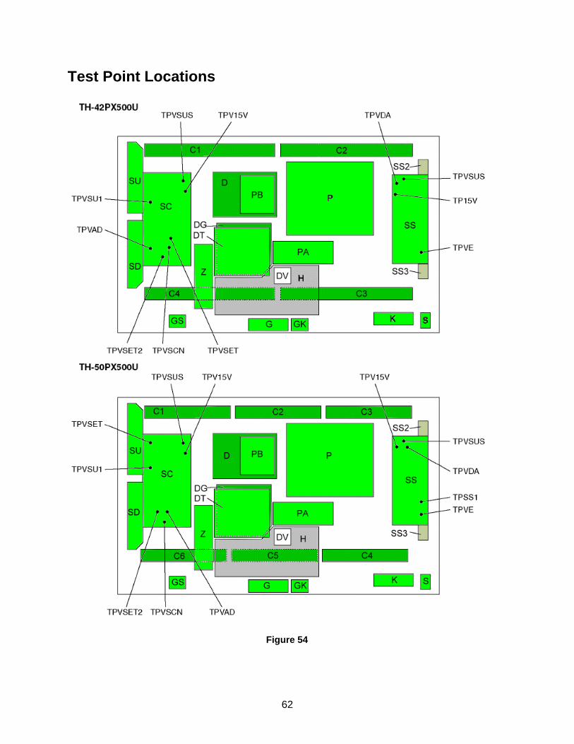
Test Point Locations
Figure 54
62

Troubleshooting
No Picture or Partial Picture
NOTE: Please utilize this diagnostic flowchart after confirming that all input signals have the same problem.
Check the D
Board.
Is there a picture in any portion of the
screen?
No
Yes
Is the SC Board LED
illuminated or is the waveform at TPSC1 ok? See Ref. *1 on
page 66.
Yes
No
Is the SC Board LED
illuminated or is the waveform at TPSS1 ok? See Ref. *2 on
page 66.
No
Yes
The SC Board is probably defective.
SS Board is probably defective.
The D Board is probably defective.
Is there 70V (VDA) at pins 1
and 2 of the connector
SS12?
No
Check the P board. Yes
Is the picture black or monochromatic
/ noisy?
Is the picture noisy or
mono- chromatic?
No
Go to step 3.
Go to step 2.
Go to step 1.
Check the DG or
D Board.
Yes
Monochromatic or noisy Enter the
Self-Check mode and check if “Panel” is OK?
Monochromatic
Yes
No Is the panel on?
63

Step 1 Step 2 Step 3
Is the waveform at TPSC1 ok? See Ref. *3 on
page 66.
Is the SCAN
CONTROL PULSE
from the D Board to the SC Board OK?
(Go to <Check Point>
on page 66.)
Check the D
board
Check the SC board.
NoNo
Yes Check the DG or
D board.
Yes
No
Check the D board.
Yes
No Check the DG board.
Is the LVDS signal output
from the DG Board to the D Board OK?
(Go to <Check Point> on page 66.)
Yes
Check the P board.
No Is the Vda voltage at
TP_VDA of the SS board OK?
Is there a dark
picture?
Yes
Go to step 1
Go to Step 4
64

Step 1
Is the waveform at TPSS1 ok?
See Ref. *4 on page 66.
No
Yes
Is the 15V at TP_15V on the SS Board OK?
No
Yes
Check the P board.
Check the DG or D board. Check the
D board.
No Is the
SUSTAIN CONTROL PULSE from the D Board to the SS Board OK? (Go to
<Check Point> on page 66.)
Yes
Check the SS board.
No
Go to Step 5
Check the SU or SC
board.
Yes
No
No lower half Check the SD or SC
board.
Is the picture
problem in theupper half of the screen?
Is the picture
problem in the upper or lower
half of the screen?
Yes, upper or lower half
Step 4
65

Scan and Sustain Drive Waveform
Figure 55
Scan and Sustain Drive Check points
Figure 56
66

Go to Step 6
Upper left of the screen
Vertical line
No picture
Is there no picture or a
wide vertical line at the upper
left of the screen?
D Board (or C2 board)
PDP Panel
Where is the picture problem?
Right half or left half of the screen
Left half of the screen?
No (right half)
D Board (or C1 & C4 board)
Yes (left half)
D Board (or C2 & C3 board)
Upper right of the screen
Vertical line
No picture
Is there no picture or a
wide vertical line at the upper right
of the screen?
D Board (or C1 board)
PDP Panel- See the section entitled
Vertical line problem.
<HD model>--- 42 / 37 inch
Step 5
67

Step 6
<SD model>--- 42 / 37 inch
Where is the picture problem?
Right half or left half of the screen
Left half of the
screen?
No (right half)
Yes (left half)
Vertical line
PDP Panel
No picture D Board (or C1 board)
Is there no picture or a
wide vertical line at the right half of
the screen?
Vertical linePDP Panel
No picture
D Board (or C2 board)
Is there no picture or a wide
vertical line at the left half of the screen?
Go to step 6.
Lower right of the screen
Vertical line
No picture
D Board (or C4 board)
Is there no picture or a
wide vertical line at the lower right of the
screen?
PDP Panel
Lower left of the screen
Vertical line
No picture
D Board (or C3 board)
Is there no picture or a
wide vertical line at the lower left of the screen?
PDP Panel
68

Step 6
Upper middle of the screen
Vertical line
PDP Panel
No picture
D Board (or C2 board)
Go to Step 6
Upper left of the screen
Vertical
No picture
D Board (or C3 board)
Is there no picture or a wide vertical line at the upper left of the
screen?
PDP Panel
Is there no picture or a wide vertical line at the
upper middle of the screen?
Where is the picture problem?
One third of the left, middle or right of the screen
Left?
No (right or middle)
D Board (or C2 & C5
board)
No (middle)
Yes
D Board (or C1 &
C6 board)
Right?
Yes
D Board (or C3 & C4 board)
Upper right of the screen
Vertical line
No picture
Is there no picture or a wide
vertical line at the upper right of the
screen?
D Board (or C1 board)
PDP Panel- See the section entitled
Vertical line problem.
<HD model>--- 50 inch
69

Step 6
Lower left of the screen
Vertical line PDP Panel
No picture
D Board (or C4 board)
Lower middle of the screen
Vertical line PDP Panel
No picture
D Board (or C5 board)
Is there no picture or a wide vertical line at the
lower middle of the screen?
Lower right of the screen
Vertical line
No picture
Check the D Board (or C6 board)
Is there no picture or a wide vertical line at the lower right of the
screen?
PDP Panel
Is there no picture or a wide vertical line at the lower left of the
screen?
70

Vertical line problems Figure 57 Thin vertical line or no picture in one block A thin vertical line or picture in ¼ of the area driven by a C board indicates a defective driver IC that is mounted on the ribbon cable that connects the C board to the panel. To resolve this problem the panel has to be replaced. A number of blocks do not light up The likelihood of all four driver ICs of the panel being defective is very small. Such a defect usually indicates that the C board may be defective or the D board may not be providing the drive data for the C board. To resolve this problem, replace the C board first. If the problem persists, replace the D board.
71

Picture ok, Sound NG
Is there no sound
from all input sources?
Yes
Check the Z board and speakers.
Yes
Check the DT board.
Check the H board.
No Is there
sound from the AV
terminal?
No sound from digital TV reception
Yes
Yes
Check the TA board.
Check the H board.
NoIs there
sound from the AV
terminal?
No sound from analog TV reception
No
Check the H board.
No Is there
sound from the program out jacks?
72

No picture, no sound
Check the DT board.
No picture and sound from digital TV
reception
Input Source check
Check the H board.
No picture and sound from the AV terminal
Yes
Check the TA board.
Check the H board.
No Is the
picture and sound of the AV terminal
ok?
No picture and no sound from analog TV
reception
73

No picture, sound ok
Yes
Check the DG board.
No Is there a
picture from the AV
terminal?
Check the DT board.
No picture from digital TV reception
Check the H board.
No picture from the AV terminal
No picture from analog TV reception
Yes
Check the H board.
No Is there picture from one of the
AV inputs?
Input Source check
Yes
Check the TA board.
Check the H and DG
board.
No Is there a
picture from the AV
terminal?
74

How to determine whether the D board or SC board is defective?
Figure 58 Note: All SCAN CONTROL PULSES are located at pins 2, 3, 4, 6, 7, 8, 9, 13, 17, 18, 19, and 20 of connector SC20-D20. A missing waveform at one of the pins with the exception of pins 8, 9, and 13 will cause the power LED to blink.
75

Additional Troubleshooting Hints
Symptom 1: Picture Noise - Many vertical lines are seen all over the screen. Cause: The voltage of the address period of the Scan Drive Signal at pin 8 of
connector SC20/D20 has dropped. The problem is the D board.
Figure 59 Symptom 2: Picture Noise - Part of the previous picture is visible on the screen. Cause: The VSET (Initialization) pulse of the Scan Drive signal at pin 9 of
connector SC20/D20 has dropped. The problem is the D board. Figure 59a
76

Symptom 3: Picture Noise - Part of the previous picture remains on the screen. Cause: There is no Erase Pulse in the Scan Drive Signal at pin 13 of connector
SC20/D20. The problem is the D board.
Figure 60 The approach to find the defective board is to check the pins of the connector listed in the table below.
Check point
SC20 or D20 Connector
Pin 8
Pin 9
Pin 13
Defect Board
OK OK OK SC Board
NG NG OK D Board
OK NG OK D Board
OK OK NG D Board
NG NG NG D Board
Table 14
77

How to determine whether the D board or SS board is defective?
Figure 61 Note: All SUSTAIN CONTROL PULSES are located at pins 3, 4, 5, 6, 7, and 8 of one of the C (see the table above) and SS44 connectors. A missing waveform at one of the pins with the exception of pin 4 will cause the power LED to blink.
78

Symptom: Dark picture - Dark screen with a dim picture. Cause: There is no Sustain Control Pulse at pin 4 of the C or SS connector listed
below. The voltage Ve of the initializing and address period of Sustain Drive Signal is missing. The problem is the D board.
Figure 62
The approach to find the defective board is to check pin 4 of the connectors listed in the table below.
Check Point
Model
Connector NO.
Pin NO.
37"HD
C32
42"SD
C23
42"HD
C32
50"HD
SS44
4
Defective Board
OK
SS Board
NG
D Board
Table 15
79

Glossary and Acronyms ATSC (Advanced Television Systems Committee) Standardization body that developed the Digital Television Terrestrial formats. CDS (Current Directory Structure) DCF (Design rule for Camera File system) Unified standard established by Japan Electronics and Information Technology Industries Association (JEITA). DCM (Digital Carrier Module) A PCMCIA type card that is provided by the Cable operator FAT (Forward Application Transport) FAT 12 or FAT 16: File systems used in formatting the memory cards. FDC STATUS (Forward Data Channel Status) POD (Point Of Deployment) PCR (Program Clock Reference) PID (Packet Identification Data) HDMI (High Definition Multimedia Interface) Interface that supports every uncompressed digital format as well as all existing multi-channel audio format on a single cable JPEG (Joint Photographic Experts Group) A system used for compressing/decoding color still pictures. MPAA (Motion Picture Association of America) Guild governing rating assignments to movies NTSC (National Television Systems Committee) Standardization body that developed the Analog Television Terrestrial formats. Password A four-digit code a user must provide in order to perform a function.
80

![[XLS]diagramasde.comdiagramasde.com/diagramas/otros2/ListadePrecios.xls · Web viewMINI ECO MIXER CON AMPLIFICADOR PET PROLONGACION EJE TANDEM PF3MM PROTECTOR DE FOQUITOS 3MM PF5MM](https://static.fdocuments.us/doc/165x107/5aa360ad7f8b9a84398e4a79/xls-viewmini-eco-mixer-con-amplificador-pet-prolongacion-eje-tandem-pf3mm-protector.jpg)