Technical Data - NXP
32
© Freescale Semiconductor, Inc., 2005. All rights reserved. Freescale Semiconductor Technical Data Freescale reserves the right to change the detail specifications as may be required to permit improvements in the design of its products. MC145170-2/D Rev. 5, 1/2005 MC145170-2 SCALE 2:1 Package Information D Suffix Plastic DIP Package Case 751B Package Information DT Suffix TSSOP Package Case 948C Package Information P Suffix SOG Package Case 648 Ordering Information Device Operating Temperature Range Package MC145170P2 T A = -40 to 85°C Plastic DIP MC145170D2 SOG-16 MC145170DT2 TSSOP-16 1 Introduction The new MC145170-2 is pin-for-pin compatible with the MC145170-1. A comparison of the two parts is shown in Table 1 on page 2. The MC145170-2 is recommended for new designs and has a more robust power-on reset (POR) circuit that is more responsive to momentary power supply interruptions. The two devices are actually the same chip with mask options for the POR circuit. The more robust POR circuit draws approximately 20 µA additional supply current. Note that the maximum specification of 100 µA quiescent supply current has not changed. The MC145170-2 is a single-chip synthesizer capable of direct usage in the MF, HF, and VHF bands. A special architecture makes this PLL easy to program. Either a bit- or byte-oriented format may be used. Due to the patented BitGrabber™ registers, no address/steering bits are required for random access of the three registers. Thus, tuning can be accomplished via a 2-byte serial transfer to the 16-bit N register. MC145170-2 PLL Frequency Synthesizer with Serial Interface Contents 1 Introduction . . . . . . . . . . . . . . . . . . . . . . . . . . 1 2 Electrical Characteristics . . . . . . . . . . . . . . . 3 3 Pin Connections . . . . . . . . . . . . . . . . . . . . . . . 9 4 Design Considerations . . . . . . . . . . . . . . . . 18 5 Packaging . . . . . . . . . . . . . . . . . . . . . . . . . . . 29
Transcript of Technical Data - NXP

© Freescale Semiconductor, Inc., 2005. All rights reserved.
Freescale SemiconductorTechnical Data
Freescale reserves the right to change the detail specifications as may be required to permit improvements in the design of its products.
MC145170-2/DRev. 5, 1/2005
MC145170-2
SCALE 2:1
Package InformationD Suffix
Plastic DIP PackageCase 751B
Package InformationDT Suffix
TSSOP PackageCase 948C
Package InformationP Suffix
SOG PackageCase 648
Ordering Information
DeviceOperating
Temperature RangePackage
MC145170P2
TA = -40 to 85°C
Plastic DIP
MC145170D2 SOG-16
MC145170DT2 TSSOP-16
1 IntroductionThe new MC145170-2 is pin-for-pin compatible with the MC145170-1. A comparison of the two parts is shown in Table 1 on page 2. The MC145170-2 is recommended for new designs and has a more robust power-on reset (POR) circuit that is more responsive to momentary power supply interruptions. The two devices are actually the same chip with mask options for the POR circuit. The more robust POR circuit draws approximately 20 µA additional supply current. Note that the maximum specification of 100 µA quiescent supply current has not changed.
The MC145170-2 is a single-chip synthesizer capable of direct usage in the MF, HF, and VHF bands. A special architecture makes this PLL easy to program. Either a bit- or byte-oriented format may be used. Due to the patented BitGrabber™ registers, no address/steering bits are required for random access of the three registers. Thus, tuning can be accomplished via a 2-byte serial transfer to the 16-bit N register.
MC145170-2PLL Frequency Synthesizer with Serial Interface
Contents1 Introduction . . . . . . . . . . . . . . . . . . . . . . . . . . 12 Electrical Characteristics . . . . . . . . . . . . . . . 33 Pin Connections . . . . . . . . . . . . . . . . . . . . . . . 94 Design Considerations . . . . . . . . . . . . . . . . 185 Packaging . . . . . . . . . . . . . . . . . . . . . . . . . . . 29
MC145170-2 Technical Data, Rev. 5
2 Freescale Semiconductor
Introduction
The device features fully programmable R and N counters, an amplifier at the fin pin, on-chip support of an external crystal, a programmable reference output, and both single- and double-ended phase detectors with linear transfer functions (no dead zones). A configuration (C) register allows the part to be configured to meet various applications. A patented feature allows the C register to shut off unused outputs, thereby minimizing noise and interference.
In order to reduce lock times and prevent erroneous data from being loaded into the counters, a patented jam-load feature is included. Whenever a new divide ratio is loaded into the N register, both the N and R counters are jam-loaded with their respective values and begin counting down together. The phase detectors are also initialized during the jam load.
Operating Voltage Range: 2.7 to 5.5 V Maximum Operating Frequency:
185 MHz @ Vin = 500 mVpp, 4.5 V Minimum Supply 100 MHz @ Vin = 500 mVpp, 3.0 V Minimum Supply
Operating Supply Current: 0.6 mA @ 3.0 V, 30 MHz 1.5 mA @ 3.0 V, 100 MHz 3.0 mA @ 5.0 V, 50 MHz 5.8 mA @ 5.0 V, 185 MHz
Operating Temperature Range: -40 to 85°C R Counter Division Range: 1 and 5 to 32,767 N Counter Division Range: 40 to 65,535 Programs through Standard Serial Peripheral Interface (SPI) See Application Notes AN1207/D and AN1671/D Contact Freescale for MC145170 control software.
Table 1. Comparision of the PLL Frequency Synthesizers
Parameter MC145170-2 MC145170-1
Minimum Supply Voltage 2.7 V 2.5 V
Maximum Input Current, fin 150 µA 120 µA
Dynamic Characteristics, fin (Figure 26) Unchanged -
Power-On Reset Circuit Improved -

Electrical Characteristics
MC145170-2 Technical Data, Rev. 5
Freescale Semiconductor 3
Figure 1. Block Diagram
2 Electrical CharacteristicsTable 2. Maximum Ratings (Voltages Referenced to VSS)
Parameter Symbol Value Unit
DC Supply Voltage VDD -0.5 to 5.5 V
DC Input Voltage Vin -0.5 to VDD + 0.5 V
DC Output Voltage Vout -0.5 to VDD + 0.5 V
DC Input Current, per Pin Iin ±10 mA
DC Output Current, per Pin Iout ±20 mA
DC Supply Current, VDD and VSS Pins IDD ±30 mA
Power Dissipation, per Package PD 300 mW
Storage Temperature Tstg -65 to 150 °C
Lead Temperature, 1 mm from Case for 10 seconds
TL 260 °C
Note: Maximum Ratings and ESD
1. Maximum Ratings are those values beyond which damage to the device may occur. Functional operation should be restricted to the limits in the Electrical Characteristics tables or Pin Descriptions section.
2. ESD data available upon request.
BitGrabber R Register15 Bits
Lock Detector and Control
BitGrabber C Register8 Bits
Phase/Frequency Detector Aand Control
POR
Phase/Frequency Detector Band Control
BitGrabber N Register16 Bits
OSC
ShiftRegister
And ControlLogic
ENB
OSCin
Din
CLK
OSCout
fin
1
2
7
5
4
3
15
16
16
LD
PDout
fRfV
10
1514
13
11
9
Pin 16 = VDDPin 12 = VSS
InputAMP
6
4-StageReference
DividerREFout
3
Dout 8
fV Control
fR
fV
15-stage R Counter fR Control
16-Stage N Counter
This device contains 4,800 active transistors.
MC145170-2 Technical Data, Rev. 5
4 Freescale Semiconductor
Electrical Characteristics
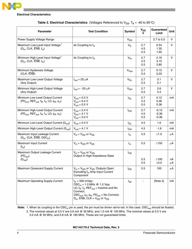
Table 3. Electrical Characteristics (Voltages Referenced to VSS, TA = -40 to 85°C)
Parameter Test Condition SymbolVDD
VGuaranteed
LimitUnit
Power Supply Voltage Range VDD - 2.7 to 5.5 V
Maximum Low-Level Input Voltage1 (Din, CLK, ENB, fin)
dc Coupling to fin VIL 2.74.55.5
0.541.351.65
V
Minimum High-Level Input Voltage1
(Din, CLK, ENB, fin)dc Coupling to fin VIH 2.7
4.55.5
2.163.153.85
V
Minimum Hysteresis Voltage (CLK, ENB)
VHys 2.75.5
0.150.20
V
Maximum Low-Level Output Voltage (Any Output)
Iout = 20 µA VOL 2.75.5
0.10.1
V
Minimum High-Level Output Voltage (Any Output)
Iout = - 20 µA VOH 2.75.5
2.65.4
V
Minimum Low-Level Output Current (PDout, REFout, fR, fV, LD, φR, φV)
Vout = 0.3 VVout = 0.4 VVout = 0.5 V
IOL 2.74.55.5
0.120.360.36
mA
Minimum High-Level Output Current (PDout, REFout, fR, fV, LD, φR, φV)
Vout = 2.4 VVout = 4.1 VVout = 5.0 V
IOH 2.74.55.5
-0.12-0.36-0.36
mA
Minimum Low-Level Output Current (Dout) Vout = 0.4 V IOL 4.5 1.6 mA
Minimum High-Level Output Current (Dout) Vout = 4.1 V IOH 4.5 -1.6 mA
Maximum Input Leakage Current (Din, CLK, ENB, OSCin)
Vin = VDD or VSS Iin 5.5 ±1.0 µA
Maximum Input Current (fin)
Vin = VDD or VSS Iin 5.5 ±150 µA
Maximum Output Leakage Current (PDout) (Dout)
Vin = VDD or VSS, Output in High-Impedance State
IOZ
5.55.5
±100±5.0
nAµA
Maximum Quiescent Supply Current Vin = VDD or VSS; Outputs Open; Excluding fin Amp Input Current Component
IDD 5.5 100 µA
Maximum Operating Supply Current fin = 500 mVpp; OSCin = 1.0 MHz @ 1.0 Vpp; LD, fR, fV, REFout = Inactive and No Connect; OSCout, φV, φR, PDout = No Connect; Din, ENB, CLK = VDD or VSS
Idd - [Note 2] mA
Note: 1. When dc coupling to the OSCin pin is used, the pin must be driven rail-to-rail. In this case, OSCout should be floated.2. The nominal values at 3.0 V are 0.6 mA @ 30 MHz, and 1.5 mA @ 100 MHz. The nominal values at 5.0 V are
3.0 mA @ 50 MHz, and 5.8 mA @ 185 MHz. These are not guaranteed limits.

Electrical Characteristics
MC145170-2 Technical Data, Rev. 5
Freescale Semiconductor 5
Table 4. AC Interface Characteristics ( TA = -40 to 85°C, CL = 50 pF, Input tr = tf = 10 ns, unless otherwise noted.)
Parameter SymbolFigure
No.VDD
VGuaranteed
LimitUnit
Serial Data Clock Frequency (Note: Refer to Clock tw Below) fclk 2 2.74.55.5
dc to 3.0dc to 4.0dc to 4.0
MHz
Maximum Propagation Delay, CLK to Dout tPLH, tPHL 2, 6 2.74.55.5
1508585
ns
Maximum Disable Time, Dout Active to High Impedance tPLZ, tPHZ 3, 7 2.74.55.5
300200200
ns
Access Time, Dout High Impedance to Active tPZL, tPZH 3, 7 2.74.55.5
0 to 2000 to 1000 to 100
ns
Maximum Output Transition Time, Dout CL = 50 pF
tTLH, tTHL 2, 6 2.74.55.5
1505050
ns
CL = 200 pF 2, 6 2.74.55.5
900150150
ns
Maximum Input Capacitance - Din, ENB, CLK Cin - 10 pF
Maximum Output Capacitance - Dout Cout - 10 pF
Table 5. Timing Requirements (TA = -40 to 85°C, Input tr = tf = 10 ns, unless otherwise noted.)
Parameter SymbolFigure
No.VDD
VGuaranteed
LimitUnit
Minimum Setup and Hold Times, Din vs CLK tsu, th 4 2.74.55.5
554040
ns
Minimum Setup, Hold, and Recovery Times, ENB vs CLK tsu, th, trec 5 2.74.55.5
135100100
ns
Minimum Inactive-High Pulse Width, ENB tw(H) 5 2.74.55.5
400300300
ns
Minimum Pulse Width, CLK tw 2 2.74.55.5
166125125
ns
Maximum Input Rise and Fall Times, CLK tr, tf 2 2.74.55.5
100100100
µs
MC145170-2 Technical Data, Rev. 5
6 Freescale Semiconductor
Electrical Characteristics
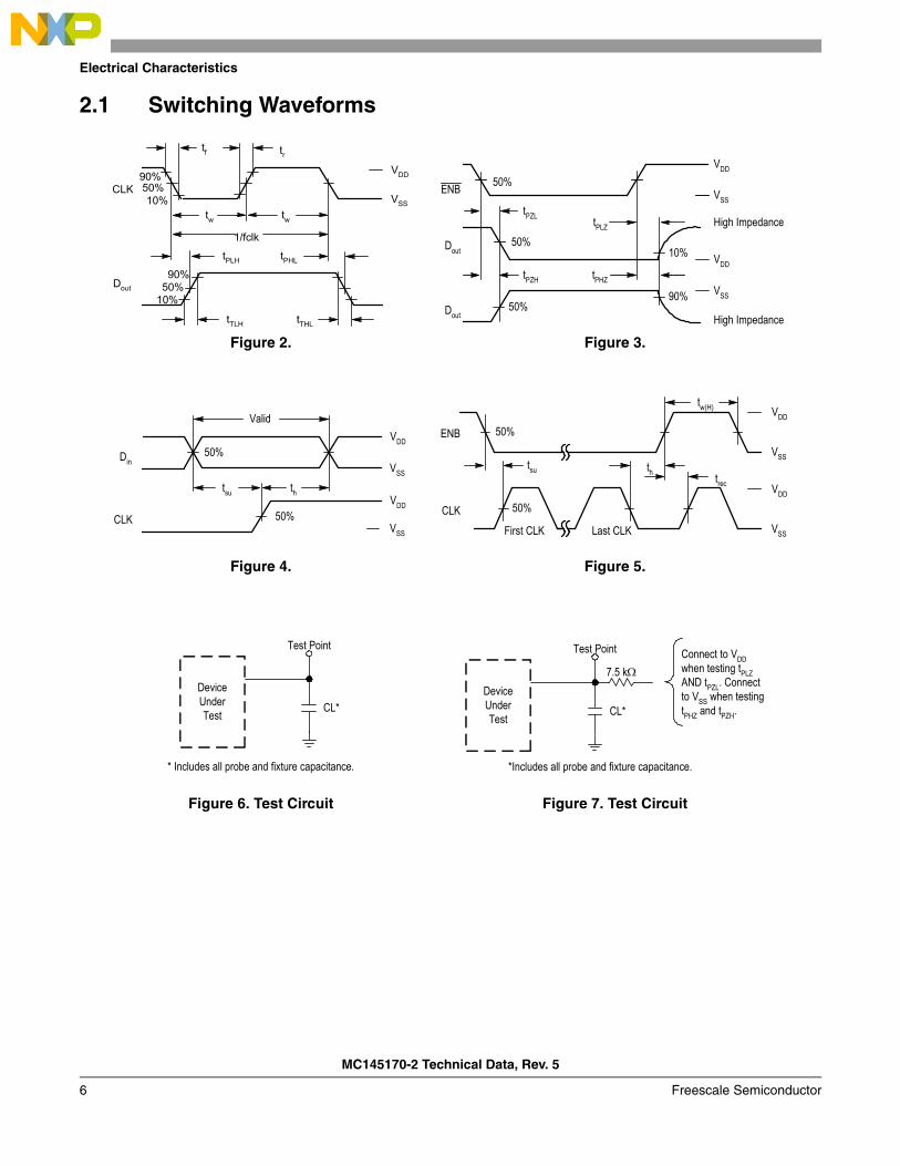
2.1 Switching Waveforms
10%
VDD
VSS
1/fclk
Dout
CLK
90%50%
90%50%10%
tPLH tPHL
tTLH tTHL
twtw
tf tr
ENB
Dout
Dout50%
VDD
VSS
50%
tPZH
tPZL tPLZ
50%
tPHZ
10%
90%
VDD
VSS
High Impedance
High Impedance
Figure 2. Figure 3.
Din
CLK
50%
Valid
50%
tsu thVDD
VSS
VDD
VSS
CLK
ENB
50%
tsu th
First CLK Last CLK
trec
50%
VDD
VSS
VDD
VSS
tw(H)
Figure 4. Figure 5.
* Includes all probe and fixture capacitance.
Test Point
DeviceUnderTest CL*
Test Point
DeviceUnderTest CL*
*Includes all probe and fixture capacitance.
7.5 kΩ
Connect to VDDwhen testing tPLZAND tPZL. Connectto VSS when testingtPHZ and tPZH.
Figure 6. Test Circuit Figure 7. Test Circuit

Electrical Characteristics
MC145170-2 Technical Data, Rev. 5
Freescale Semiconductor 7
Figure 8. Test Circuit, fin
Table 6. Loop Specifications (TA = -40 to 85°C)
Parameter Test Condition SymbolFigure
No.VDD
V
Guaranteed RangeUnit
Min Max
Input Frequency, fin [Note] Vin ≥ 500 mVpp Sine Wave, N Counter Set to Divide Ratio Such that fV ≤ 2.0 MHz
f 8 2.73.04.55.5
5.05.02545
80100185185
MHz
Input Frequency, OSCin Externally Driven with ac-coupled Signal
Vin ≥ 1.0 Vpp Sine Wave, OSCout = No Connect, R Counter Set to Divide Ratio Such that fR ≤ 2 MHz
f 9 2.73.04.55.5
1.0*1.0*1.0*1.0*
22253035
MHz
Crystal Frequency, OSCin and OSCout
C1 ≤ 30 pF C2 ≤ 30 pF Includes Stray Capacitance
fXTAL 11 2.73.04.55.5
2.02.02.02.0
12121515
MHz
Output Frequency, REFout CL = 30 pF fout 12, 14 2.74.55.5
dcdcdc
-1010
MHz
Operating Frequency of the Phase Detectors
f 2.74.55.5
dcdcdc
-2.02.0
MHz
Output Pulse Width, φR, φV, and LD
fR in Phase with fV CL = 50 pF
tw 13, 14 2.74.55.5
-2016
-10090
ns
Output Transition Times, φR, φV, LD, fR, and fV
CL = 50 pF tTLH,tTHL
13, 14 2.74.55.5
---
-6560
ns
Input Capacitance fin OSCin
Cin --
--
--
7.07.0
pF
* If lower frequency is desired, use wave shaping or higher amplitude sinusoidal signal in ac-coupled case. Also, see Figure 25 on page 22 for dc coupling.
Sine WaveGenerator
100 pF
MC145170-2
Test Point
V+VDD
fin fV
Vin
50 Ω*VSS
*Characteristic impedance

MC145170-2 Technical Data, Rev. 5
8 Freescale Semiconductor
Electrical Characteristics
Figure 9. Test Circuit, OSC Circuitry Externally Driven [Note]
Figure 10. Circuit to Eliminate Self-Oscillation, OSC Circuitry Externally Driven [Note]
NOTEUse the circuit of Figure 10 to eliminate self-oscillation of the OSCin pin when the MC145170-2 has power applied with no external signal applied at Vin. (Self-oscillation is not harmful to the MC145170-2 and does not damage the IC.)
C1
Test Point
VDD
REFout
VSS
OSCin
OSCoutC2 V+
MC145170-2
50%REFout
1/f REFout
Figure 12. Test CircuitFigure 11. Test Circuit, OSC Circuit with Crystal
10%90%
OutputtTLHtTHL
50%
tw
Test Point
DeviceUnderTest
CL*
*Includes all probe and fixture capacitance.
Output
Figure 14. Test Load CircuitFigure 13. Switching Waveform
Sine WaveGenerator
50 Ω
0.01 µFTest Point
VDD
OSCin fR
Vin
V+VSS
MC145170-2OSCout
5.0 MΩ Sine WaveGenerator
50 Ω
0.01 µFTest Point
VDD
OSCin fR
Vin
V+VSS
MC145170-2OSCout
V+
1.0 MΩ
No Connect
1.0 MΩ

Pin Connections
MC145170-2 Technical Data, Rev. 5
Freescale Semiconductor 9
3 Pin Connections
3.1 Digital Interface Pins
Din Serial Data Input (Pin 5)
The bit stream begins with the most significant bit (MSB) and is shifted in on the low-to-high transition of CLK. The bit pattern is 1 byte (8 bits) long to access the C or configuration register, 2 bytes (16 bits) to access the N register, or 3 bytes (24 bits) to access the R register. Additionally, the R register can be accessed with a 15-bit transfer (see Table 7). An optional pattern which resets the device is shown in Figure 15. The values in the C, N, and R registers do not change during shifting because the transfer of data to the registers is controlled by ENB.
The bit stream needs neither address nor steering bits due to the innovative BitGrabber registers. Therefore, all bits in the stream are available to be data for the three registers. Random access of any register is provided (i.e., the registers may be accessed in any sequence). Data is retained in the registers over a supply range of 2.7 to 5.5 V. The formats are shown in Figures 15, 16, 17, and 18.
Din typically switches near 50% of VDD to maximize noise immunity. This input can be directly interfaced to CMOS devices with outputs guaranteed to switch near rail-to-rail. When interfacing to NMOS or TTL devices, either a level shifter (MC74HC14A, MC14504B) or pull-up resistor of 1 to 10 kΩ must be used. Parameters to consider when sizing the resistor are worst-case IOL of the driving device, maximum tolerable power consumption, and maximum data rate.
CLK Serial Data Clock Input (Pin 7)
Low-to-high transitions on Clock shift bits available at Din, while high-to-low transitions shift bits from Dout. The chip's 16-1/2-stage shift register is static, allowing clock rates down to dc in a continuous or intermittent mode.
Four to eight clock cycles followed by five clock cycles are needed to reset the device; this is optional. Eight clock cycles are required to access the C register. Sixteen clock cycles are needed for the N register. Either 15 or 24 cycles can be used to access the R register (see Table 7 and Figures 15, 16, 17, and 18). For cascaded devices, see Figures 27 to 34.
Table 7. Register Access(MSBs are shifted in first, C0, N0, and R0 are the LSBs)
Numberof Clocks
AccessedRegister
BitNomenclature
9 to 138
1615 or 24
Other Values ≤ 32Values > 32
See Figure 15C RegisterN RegisterR Register
NoneSee Figures 27 to 34
(Reset)C7, C6, C5, . . ., C0
N15, N14, N13, . . ., N0R14, R13, R12, . . ., R0

MC145170-2 Technical Data, Rev. 5
10 Freescale Semiconductor
Pin Connections
CLK typically switches near 50% of VDD and has a Schmitt-triggered input buffer. Slow CLK rise and fall times are allowed. See the last paragraph of Din for more information.
NOTETo guarantee proper operation of the power-on reset (POR) circuit, the CLK pin must be held at the potential of either the VSS or VDD pin during power up. That is, the CLK input should not be floated or toggled while the VDD pin is ramping from 0 to at least 2.7 V. If control of the CLK pin is not practical during power up, the initialization sequence shown in Figure 15 must be used.
ENB Active-Low Enable Input (Pin 6)
This pin is used to activate the serial interface to allow the transfer of data to/from the device. When ENB is in an inactive high state, shifting is inhibited, Dout is forced to the high-impedance state, and the port is held in the initialized state. To transfer data to the device, ENB (which must start inactive high) is taken low, a serial transfer is made via Din and CLK, and ENB is taken back high. The low-to-high transition on ENB transfers data to the C, N, or R register depending on the data stream length per Table 7.
NOTETransitions on ENB must not be attempted while CLK is high. This puts the device out of synchronization with the microcontroller. Resynchronization occurs when ENB is high and CLK is low.
This input is also Schmitt-triggered and switches near 50% of VDD, thereby minimizing the chance of loading erroneous data into the registers. See the last paragraph of Din for more information.
Dout Three-State Serial Data Output (Pin 8)
Data is transferred out of the 16-1/2-stage shift register through Dout on the high-to-low transition of CLK. This output is a No Connect, unless used in one of the manners discussed below.
Dout could be fed back to an MCU/MPU to perform a wrap-around test of serial data. This could be part of a system check conducted at power up to test the integrity of the system's processor, PC board traces, solder joints, etc.
The pin could be monitored at an in-line QA test during board manufacturing.
Finally, Dout facilitates troubleshooting a system and permits cascading devices.
3.2 Reference Pins
OSCin /OSCout Reference Oscillator Input/Output (Pins 1, 2)
These pins form a reference oscillator when connected to terminals of an external parallel-resonant crystal. Frequency-setting capacitors of appropriate values as recommended by the crystal supplier are connected

Pin Connections
MC145170-2 Technical Data, Rev. 5
Freescale Semiconductor 11
from each pin to ground (up to a maximum of 30 pF each, including stray capacitance). An external feedback resistor of 1.0 to 5.0 MΩ is connected directly across the pins to ensure linear operation of the amplifier. The required connections for the components are shown in Figure 11.
5 MΩ is required across the OSCin and OSCout pins in the ac-coupled case (see Figure 9 or alternate circuit Figure 10). OSCout is an internal node on the device and should not be used to drive any loads (i.e., OSCout is unbuffered). However, the buffered REFout is available to drive external loads.
The external signal level must be at least 1 Vpp; the maximum frequencies are given in Table 6, the Loop Specifications table on page 7. These maximum frequencies apply for R Counter divide ratios as indicated in the table. For very small ratios, the maximum frequency is limited to the divide ratio times 2 MHz. (Reason: the phase/frequency detectors are limited to a maximum input frequency of 2 MHz.)
If an external source is available which swings virtually rail-to-rail (VDD to VSS), then dc coupling can be used. In the dc-coupled case, no external feedback resistor is needed. OSCout must be a No Connect to avoid loading an internal node on the device, as noted above. For frequencies below 1 MHz, dc coupling must be used. The R counter is a static counter and may be operated down to dc. However, wave shaping by a CMOS buffer may be required to ensure fast rise and fall times into the OSCin pin. See Figure 25.
Each rising edge on the OSCin pin causes the R counter to decrement by one.
REFout Reference Frequency Output (Pin 3)
This output is the buffered output of the crystal-generated reference frequency or externally provided reference source. This output may be enabled, disabled, or scaled via bits in the C register (see Figure 16).
REFout can be used to drive a microprocessor clock input, thereby saving a crystal. Upon power up, the on-chip power-on-initialize circuit forces REFout to the OSCin divided-by-8 mode.
REFout is capable of operation to 10 MHz; see the Loop Specifications table. Therefore, divide values for the reference divider are restricted to two or higher for OSCin frequencies above 10 MHz.
If unused, the pin should be floated and should be disabled via the C register to minimize dynamic power consumption and electromagnetic interference (EMI).
3.3 Counter Output Pins
fR R Counter Output (Pin 9)
This signal is the buffered output of the 15-stage R counter. fR can be enabled or disabled via the C register (patented). The output is disabled (static low logic level) upon power up. If unused, the output should be left disabled and unconnected to minimize interference with external circuitry.
The fR signal can be used to verify the R counter's divide ratio. This ratio extends from 5 to 32,767 and is determined by the binary value loaded into the R register. Also, direct access to the phase detector via the OSCin pin is allowed by choosing a divide value of 1 (see Figure 17). The maximum frequency which the phase detectors operate is 2 MHz. Therefore, the frequency of fR must not exceed 2 MHz.
MC145170-2 Technical Data, Rev. 5
12 Freescale Semiconductor
Pin Connections
When activated, the fR signal appears as normally low and pulses high. The pulse width is 4.5 cycles of the OSCin pin signal, except when a divide ratio of 1 is selected. When 1 is selected, the OSCin signal is buffered and appears at the fR pin.
fV N Counter Output (Pin 10)
This signal is the buffered output of the 16-stage N counter. fV can be enabled or disabled via the C register (patented). The output is disabled (static low logic level) upon power up. If unused, the output should be left disabled and unconnected to minimize interference with external circuitry.
The fV signal can be used to verify the N counter's divide ratio. This ratio extends from 40 to 65,535 and is determined by the binary value loaded into the N register. The maximum frequency which the phase detectors operate is 2 MHz. Therefore, the frequency of fV must not exceed 2 MHz.
When activated, the fV signal appears as normally low and pulses high.
3.4 Loop Pins
fin Frequency Input (Pin 4)
This pin is a frequency input from the VCO. This pin feeds the on-chip amplifier which drives the N counter. This signal is normally sourced from an external voltage-controlled oscillator (VCO), and is ac-coupled into fin. A 100 pF coupling capacitor is used for measurement purposes and is the minimum size recommended for applications (see Figure 25). The frequency capability of this input is dependent on the supply voltage as listed in Table 6, Loop Specifications. For small divide ratios, the maximum frequency is limited to the divide ratio times 2 MHz. (Reason: the phase/frequency detectors are limited to a maximum frequency of 2 MHz.)
For signals which swing from at least the VIL to VIH levels listed in Table 3, the Electrical Characteristics table on page 4, dc coupling may be used. Also, for low frequency signals (less than the minimum frequencies shown in Table 6 on page 7), dc coupling is a requirement. The N counter is a static counter and may be operated down to dc. However, wave shaping by a CMOS buffer may be required to ensure fast rise and fall times into the fin pin. See Figure 25.
Each rising edge on the fin pin causes the N counter to decrement by 1.
PDout Single-Ended Phase/Frequency Detector Output (Pin 13)
This is a three-state output for use as a loop error signal when combined with an external low-pass filter. Through use of a patented technique, the detector's dead zone has been eliminated. Therefore, the phase/frequency detector is characterized by a linear transfer function. The operation of the phase/frequency detector is described below and is shown in Figure 19.POL bit (C7) in the C register = low (see Figure 16)Frequency of fV > fR or Phase of fV Leading fR: negative pulses from high impedance
Pin Connections
MC145170-2 Technical Data, Rev. 5
Freescale Semiconductor 13
Frequency of fV < fR or Phase of fV Lagging fR: positive pulses from high impedanceFrequency and Phase of fV = fR: essentially high-impedance state; voltage at pin determined by loop filterPOL bit (C7) = highFrequency of fV > fR or Phase of fV Leading fR: positive pulses from high impedanceFrequency of fV < fR or Phase of fV Lagging fR: negative pulses from high impedanceFrequency and Phase of fV = fR: essentially high-impedance state; voltage at pin determined by loop filter
This output can be enabled, disabled, and inverted via the C register. If desired, PDout can be forced to the high-impedance state by utilization of the disable feature in the C register (patented).
φR and φV Double-Ended Phase/Frequency Detector Outputs (Pins 14, 15)
These outputs can be combined externally to generate a loop error signal. Through use of a patented technique, the detector's dead zone has been eliminated. Therefore, the phase/frequency detector is characterized by a linear transfer function. The operation of the phase/frequency detector is described below and is shown in Figure 19.
POL bit (C7) in the C register = low (see Figure 16)
Frequency of fV > fR or Phase of fV Leading fR: φV = negative pulses, φR = essentially high
Frequency of fV < fR or Phase of fV Lagging fR: φV = essentially high, φR = negative pulses
Frequency and Phase of fV = fR: φV and φR remain essentially high, except for a small minimum time period when both pulse low in phase
POL bit (C7) = high
Frequency of fV > fR or Phase of fV Leading fR: φR = negative pulses, φV = essentially high
Frequency of fV < fR or Phase of fV Lagging fR: φR = essentially high, φV = negative pulses
Frequency and Phase of fV = fR: φV and φR remain essentially high, except for a small minimum time period when both pulse low in phase
These outputs can be enabled, disabled, and interchanged via the C register (patented).
LD Lock Detector Output (Pin 11)
This output is essentially at a high level with narrow low-going pulses when the loop is locked (fR and fV of the same phase and frequency). The output pulses low when fV and fR are out of phase or different frequencies (see Figure 19).
This output can be enabled and disabled via the C register (patented). Upon power up, on-chip initialization circuitry disables LD to a static low logic level to prevent a false lock signal. If unused, LD should be disabled and left open.

MC145170-2 Technical Data, Rev. 5
14 Freescale Semiconductor
Pin Connections
3.5 Power Supply
VDD Most Positive Supply Potential (Pin 16)
This pin may range from 2.7 to 5.5 V with respect to VSS.
For optimum performance, VDD should be bypassed to VSS using low-inductance capacitor(s) mounted very close to the device. Lead lengths on the capacitor(s) should be minimized. (The very fast switching speed of the device causes current spikes on the power leads.)
VSS Most Negative Supply Potential (Pin 12)
This pin is usually ground. For measurement purposes, the VSS pin is tied to a ground plane.
Figure 15. Reset Sequence
NOTES: This initialization sequence is usually not necessary because the on-chip power-on reset circuit performs the initialization function. However, this initialization sequence must be used immediately after power up if control of the CLK pin is not possible. That is, if CLK (Pin 7) toggles or floats upon power up, use the above sequence to reset the device. Also, use this sequence if power is momentarily interrupted such that the supply voltage to the device is reduced to below 2.7 V, but not down to at least 1 V (for example, the supply drops down to 2 V). This is necessary because the on-chip power-on reset is only activated when the supply ramps up from a voltage below approximately 1.0 V.
ENB
CLK
Din
Power Up
1 2 3
4 or More Clocks
51 2 3 4
Don't Cares Don't CaresOneZeroes Zero

Pin Connections
MC145170-2 Technical Data, Rev. 5
Freescale Semiconductor 15
Figure 16. C Register Access and Format (8 Clock Cycles are Used)
ENB
CLK
Din
MSB LSB
C7 C6 C5 C4 C3 C2 C1 C0
1 2 3 4 5 6 7 8 *
* At this point, the new byte is transferred to the C register and stored. No other registers are affected.
C7 - POL: Select the output polarity of the phase/frequency detectors. When set high, this bit inverts PDout and interchanges the φR function with φV as depicted in Figure 19. Also see the phase detector output pin descriptions for more information. This bit is cleared low at power up.
C6 - PDA/B: Selects which phase/frequency detector is to be used. When set high, enables the output of phase/frequency detector A (PDout) and disables phase/frequency detector B by forcing φR and φV to the static high state. When cleared low, phase/frequency detector B is enabled (φR and φV) and phase/frequency detector A is disabled with PDout forced to the high-impedance state. This bit is cleared low at power up.
C5 - LDE: Enables the lock detector output when set high. When the bit is cleared low, the LD output is forced to a static low level. This bit is cleared low at power up.
C4 - C2, OSC2 - OSC0: Reference output controls which determines the REFout characteristics as shown below. Upon power up, the bits are initialized such that OSCin/8 is selected.
C1 - fVE: Enables the fV output when set high. When cleared low, the fV output is forced to a static low level. The bit is cleared low upon power up.
C0 - fRE: Enables the fR output when set high. When cleared low, the fR output is forced to a static low level. The bit is cleared low upon power up.
C4 C3 C2 REFout Frequency
0 0 0 dc (Static Low)
0 0 1 OSCin
0 1 0 OSCin /2
0 1 1 OSCin /4
1 0 0 OSCin /8 (POR Default)
1 0 1 OSCin /16
1 1 0 OSCin /8
1 1 1 OSCin /16

MC145170-2 Technical Data, Rev. 5
16 Freescale Semiconductor
Pin Connections
Figure 17. R Register Access and Formats (Either 24 or 15 Clock Cycles Can Be Used)
÷÷÷÷÷÷
Pin Connections
MC145170-2 Technical Data, Rev. 5
Freescale Semiconductor 17
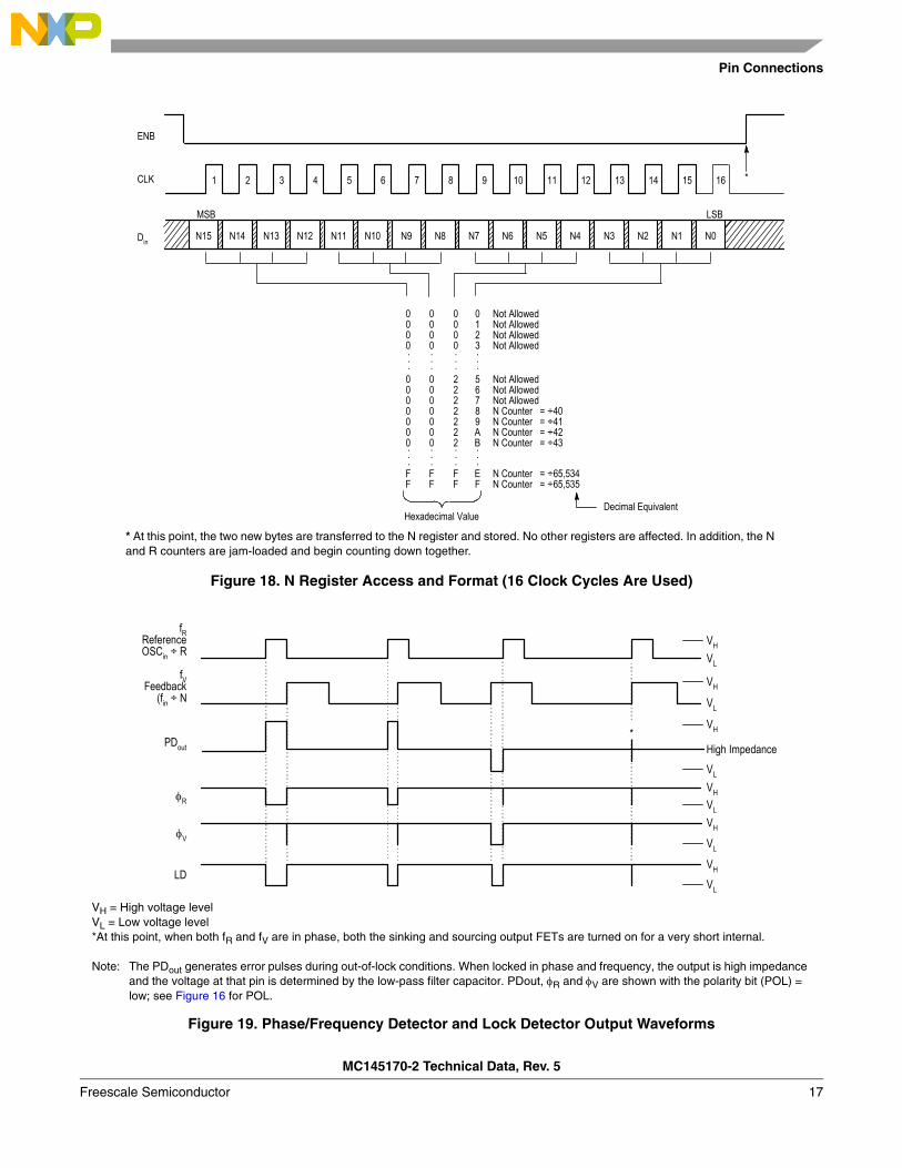
Figure 18. N Register Access and Format (16 Clock Cycles Are Used)
Figure 19. Phase/Frequency Detector and Lock Detector Output Waveforms
ENB
CLK
Din
1 2 3 4 5 6 7 8
MSB LSB
N10 N9 N8 N7 N6 N5 N4 N3 N2 N1 N0N11N12N13N14N15
9 10 11 12 13 14 15 16
0000
0000000
FF
0000
2222222
FF
0123
56789AB
EF
Not AllowedNot AllowedNot AllowedNot Allowed
Not AllowedNot AllowedNot AllowedN Counter = ÷40N Counter = ÷41N Counter = ÷42N Counter = ÷43
N Counter = ÷65,534N Counter = ÷65,535
Hexadecimal Value
0000
0000000
FF
Decimal Equivalent
*
.
...
.
.... . . .
.
...
.
.... . . .
* At this point, the two new bytes are transferred to the N register and stored. No other registers are affected. In addition, the N and R counters are jam-loaded and begin counting down together.
fRReferenceOSCin ÷ R
fVFeedback(fin ÷ N
PDout
φR
φV
LD
VH
VL
VH
VH
VH
VL
High Impedance
VH
VL
VL
VL
VH
VL
*
VH = High voltage levelVL = Low voltage level*At this point, when both fR and fV are in phase, both the sinking and sourcing output FETs are turned on for a very short internal.
Note: The PDout generates error pulses during out-of-lock conditions. When locked in phase and frequency, the output is high impedance and the voltage at that pin is determined by the low-pass filter capacitor. PDout, φR and φV are shown with the polarity bit (POL) = low; see Figure 16 for POL.
MC145170-2 Technical Data, Rev. 5
18 Freescale Semiconductor
Design Considerations
4 Design Considerations
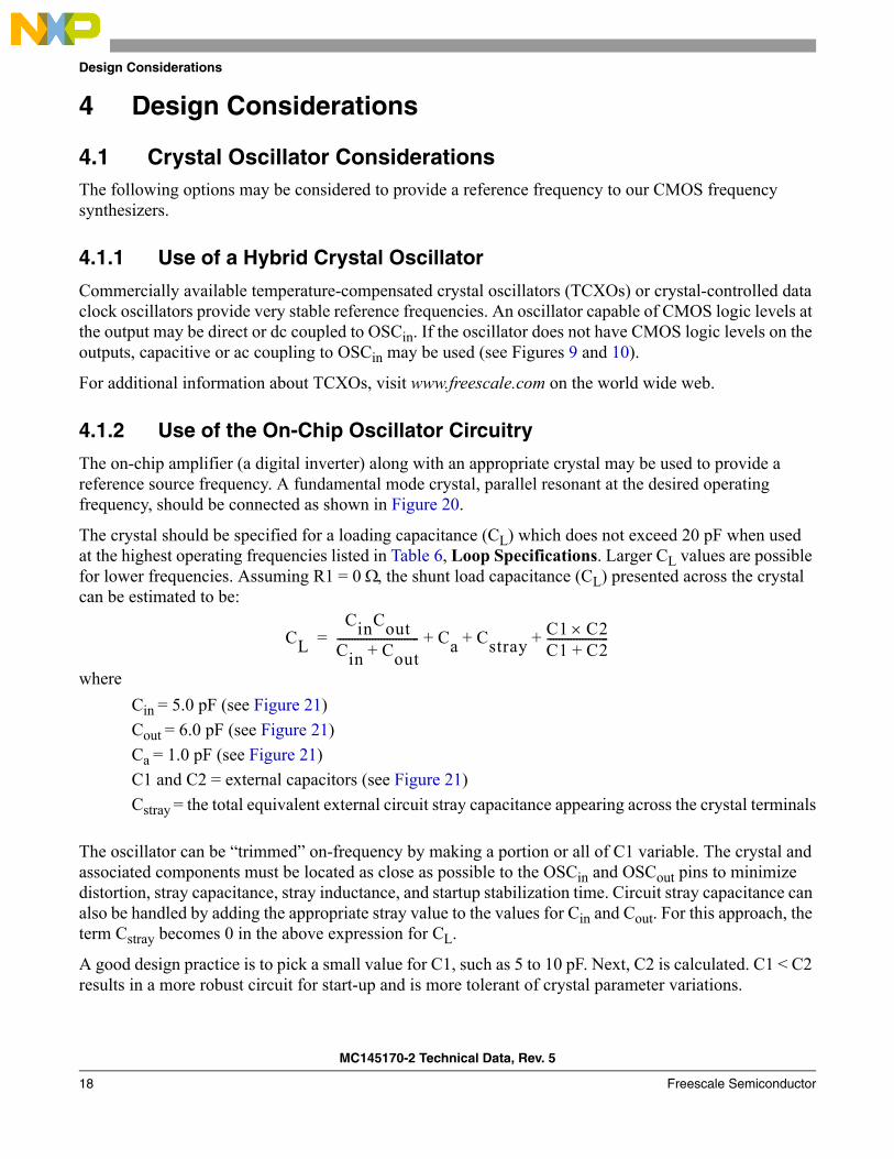
4.1 Crystal Oscillator ConsiderationsThe following options may be considered to provide a reference frequency to our CMOS frequency synthesizers.
4.1.1 Use of a Hybrid Crystal Oscillator
Commercially available temperature-compensated crystal oscillators (TCXOs) or crystal-controlled data clock oscillators provide very stable reference frequencies. An oscillator capable of CMOS logic levels at the output may be direct or dc coupled to OSCin. If the oscillator does not have CMOS logic levels on the outputs, capacitive or ac coupling to OSCin may be used (see Figures 9 and 10).
For additional information about TCXOs, visit www.freescale.com on the world wide web.
4.1.2 Use of the On-Chip Oscillator Circuitry
The on-chip amplifier (a digital inverter) along with an appropriate crystal may be used to provide a reference source frequency. A fundamental mode crystal, parallel resonant at the desired operating frequency, should be connected as shown in Figure 20.
The crystal should be specified for a loading capacitance (CL) which does not exceed 20 pF when used at the highest operating frequencies listed in Table 6, Loop Specifications. Larger CL values are possible for lower frequencies. Assuming R1 = 0 Ω, the shunt load capacitance (CL) presented across the crystal can be estimated to be:
whereCin = 5.0 pF (see Figure 21)Cout = 6.0 pF (see Figure 21)Ca = 1.0 pF (see Figure 21)C1 and C2 = external capacitors (see Figure 21)Cstray = the total equivalent external circuit stray capacitance appearing across the crystal terminals
The oscillator can be trimmed on-frequency by making a portion or all of C1 variable. The crystal and associated components must be located as close as possible to the OSCin and OSCout pins to minimize distortion, stray capacitance, stray inductance, and startup stabilization time. Circuit stray capacitance can also be handled by adding the appropriate stray value to the values for Cin and Cout. For this approach, the term Cstray becomes 0 in the above expression for CL.
A good design practice is to pick a small value for C1, such as 5 to 10 pF. Next, C2 is calculated. C1 < C2 results in a more robust circuit for start-up and is more tolerant of crystal parameter variations.
CLCinCout
Cin Cout+---------------------------- Ca Cstray
C1 C2×C1 C2+---------------------+ + +=

Design Considerations
MC145170-2 Technical Data, Rev. 5
Freescale Semiconductor 19
Power is dissipated in the effective series resistance of the crystal, Re, in Figure 22. The maximum drive level specified by the crystal manufacturer represents the maximum stress that the crystal can withstand without damage or excessive shift in operating frequency. R1 in Figure 20 limits the drive level. The use of R1 is not necessary in most cases.
To verify that the maximum dc supply voltage does not cause the crystal to be overdriven, monitor the output frequency at the REFout pin (OSCout is not used because loading impacts the oscillator). The frequency should increase very slightly as the dc supply voltage is increased. An overdriven crystal decreases in frequency or becomes unstable with an increase in supply voltage. The operating supply voltage must be reduced or R1 must be increased in value if the overdriven condition exists. The user should note that the oscillator start-up time is proportional to the value of R1.
Through the process of supplying crystals for use with CMOS inverters, many crystal manufacturers have developed expertise in CMOS oscillator design with crystals. Discussions with such manufacturers can prove very helpful.
Figure 20. Pierce Crystal Oscillator Circuit
Figure 21. Parasitic Capacitances of the Amplifier and Cstray
Figure 22. Equivalent Crystal Networks
R1*
C2C1
FrequencySynthesizer
OSCoutOSCin Rf
* May be needed in certain cases. See text.
5.0 to 10 pF
Cin Cout
CaOSCin OSCout
Cstray
21
2121
RS LS CS
Re Xe
CO
NOTE: Values are supplied by crystal manufacturer (parallel resonant crystal).

MC145170-2 Technical Data, Rev. 5
20 Freescale Semiconductor
Design Considerations
Figure 23. Phase-Locked Loop - Low Pass Filter Design
C
VCOPDoutR1
C
VCO
R2
PDoutR1
A
C
R2
C
VCOφR
φV
R1 -
+
MC33077 orequivalent(Note 3)
R1
R2
(A)
(B)
(C)
ωnKφKVCO
NR1C-------------------------=
ζNωn
2KφKVCO-----------------------------=
F s( ) 1R1sC 1+--------------------------=
ωnKφKVCO
NC R1 R2+( )------------------------------------=
ζ 0.5ωn R2C NKφKVCO-------------------------+⎝ ⎠
⎛ ⎞=
F s( )R2sC 1+
R1 R2+( )sC 1+---------------------------------------------=
ωnKφKVCO
NCR1-------------------------=
ζωnR2C
2--------------------=
F s( )R2sC 1+
R1sC--------------------------=
NOTES:1. For (C), R1 is frequently split into two series resistors; each resistor is equal to R1 divided by 2. A capacitor CC is
then placed from the midpoint to ground to further filter the error pulses. The value of CC should be such that the corner frequency of this network does not significantly affect ωn.
2. The φR and φV outputs swing rail-to-rail. Therefore, the user should be careful not to exceed the common mode input range of the op amp.
Denifitions:
N = Total Division Ratio in Feedback Loop
Kφ (Phase Detector Gain) = VDD/4p volts per radian for PDout
Kφ (Phase Detector Gain) - VDD/2p volts per radian for fV and fR
For a nominal design starting point, the user might consider a damping factor ζ = 0.7 and a natural loop frequency ωn = (2πfR/50) where fR is the frequency at the phase detector input. Larger ωn values result in faster loop lock times and, for similar sideband filtering, higher fR-related VCO standards.
KVCO VCO Gain( )2π∆fVCO∆VVCO
--------------------------=
Design Considerations
MC145170-2 Technical Data, Rev. 5
Freescale Semiconductor 21
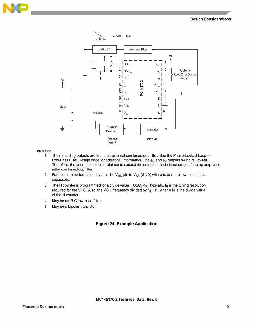
Figure 24. Example Application
MCU
ThresholdDetector
OSCin VDD
fin
OSCout φV
φR
VSS
fR
LDENB
1
2
3
4
5
6
7
8 9
10
11
12
13
14
15
16
VHF OutputBuffer
Optional
REF
Din
Dout
PDout
V+
Integrator
VHF VCO Low-pass Filter
V+
OptionalLoop Error Signals
(Note 1)
MC14
5170
-2
CLK fV
Optional(Note 5)
(Note 4)
NOTES:1. The φR and φV outputs are fed to an external combiner/loop filter. See the Phase-Locked Loop —
Low-Pass Filter Design page for additional information. The φR and φV outputs swing rail-to-rail. Therefore, the user should be careful not to exceed the common mode input range of the op amp used inthe combiner/loop filter.
2. For optimum performance, bypass the VDD pin to VSS (GND) with one or more low-inductance capacitors.
3. The R counter is programmed for a divide value = OSCin/fR. Typically, fR is the tuning resolution required for the VCO. Also, the VCO frequency divided by fR = N, wher e N is the divide value of the N counter.
4. May be an R-C low-pass filter.
5. May be a bipolar transistor.
MC145170-2 Technical Data, Rev. 5
22 Freescale Semiconductor
Design Considerations
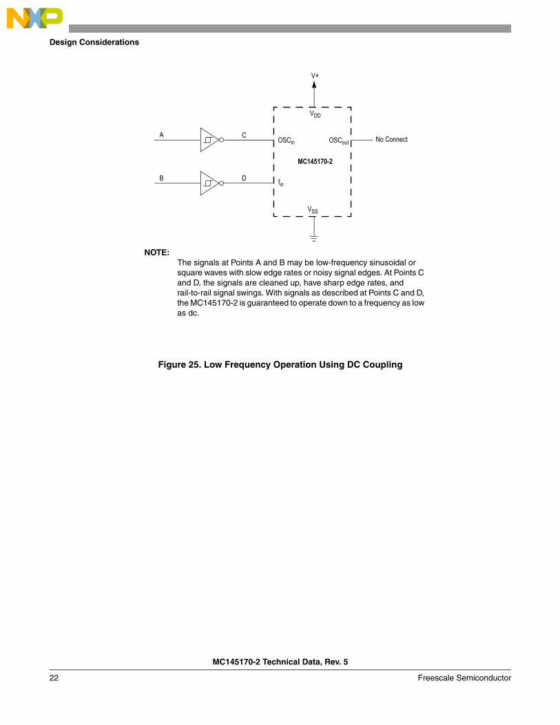
Figure 25. Low Frequency Operation Using DC Coupling
NOTE:The signals at Points A and B may be low-frequency sinusoidal or square waves with slow edge rates or noisy signal edges. At Points C and D, the signals are cleaned up, have sharp edge rates, and rail-to-rail signal swings. With signals as described at Points C and D, the MC145170-2 is guaranteed to operate down to a frequency as low as dc.
No Connect
V+
VDD
VSS
OSCin OSCout
fin
A
B
C
D
MC145170-2
Design Considerations
MC145170-2 Technical Data, Rev. 5
Freescale Semiconductor 23
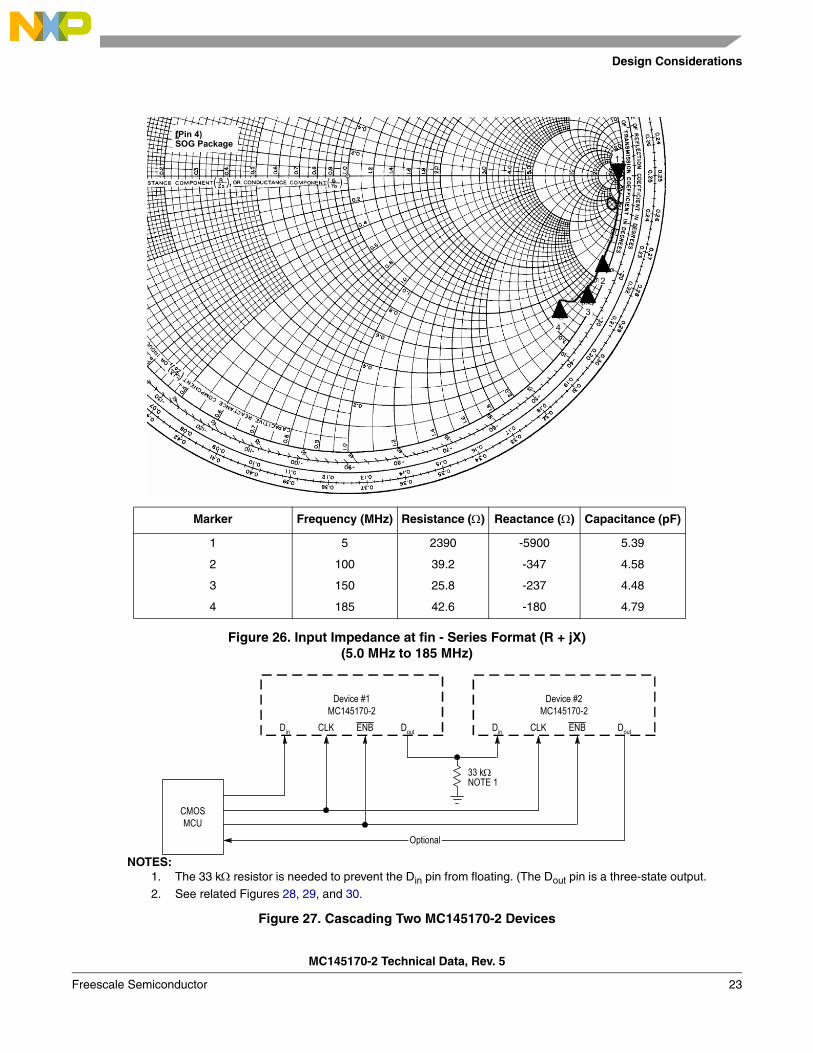
Figure 26. Input Impedance at fin - Series Format (R + jX)(5.0 MHz to 185 MHz)
Figure 27. Cascading Two MC145170-2 Devices
4
3
2
1
fin(Pin 4)SOG Package
Marker Frequency (MHz) Resistance (Ω) Reactance (Ω) Capacitance (pF)
1 5 2390 -5900 5.39
2 100 39.2 -347 4.58
3 150 25.8 -237 4.48
4 185 42.6 -180 4.79
Device #1MC145170-2
CMOSMCU
Optional
DoutENBCLKDin
Device #2MC145170-2
ENBCLKDin Dout
33 kΩNOTE 1
NOTES:1. The 33 kΩ resistor is needed to prevent the Din pin from floating. (The Dout pin is a three-state output.
2. See related Figures 28, 29, and 30.

MC145170-2 Technical Data, Rev. 5
24 Freescale Semiconductor
Design Considerations
Fig
ure
28.
Acc
essi
ng
th
e C
Reg
iste
rs o
f Tw
o C
asca
ded
MC
1451
70-2
Dev
ices
Fig
ure
29.
Acc
essi
ng
th
e R
Reg
iste
rs o
f Tw
o C
asca
ded
MC
1451
70-2
Dev
ices
NO
TE: A
t thi
s po
int,
the
new
dat
a is
tran
sfer
red
to th
e C
regi
ster
s of
bot
h de
vice
s an
d st
ored
. No
othe
r reg
iste
rs a
re a
ffect
ed.
12
78
910
1516
1718
2324
2526
3132
3334
3940
C Re
gister
Bits
of D
evice
#2in
Figur
e 27
C Re
gister
Bits
of D
evice
#1in
Figur
e 27
XX
XX
XX
C7C6
C0X
XX
C7C6
C0
ENB
CLK
D in
NOTE
NO
TE: A
t thi
s po
int,
the
new
dat
a is
tran
sfer
red
to th
e R
regi
ster
s of
bot
h de
vice
s an
d st
ored
. No
othe
r reg
iste
rs a
re a
ffect
ed.
ENB
CLK
D in
12
89
1025
2627
3031
3940
4142
4445
R Re
gister
Bits
of D
evice
#2in
Figur
e 27
R Re
gister
Bits
of D
evice
#1in
Figur
e 27
XX
XX
R14
R13
XR1
4R1
1
4849
5055
56
R7R6
R0R0
R1R9
NOTE
MC145170-2 Technical Data, Rev. 5
Freescale Semiconductor 25
Design Considerations
Fig
ure
30.
Acc
essi
ng
th
e N
Reg
iste
rs o
f T
wo
Cas
cad
ed M
C14
5170
-2 D
evic
es
NO
TE: A
t thi
s po
int,
the
new
dat
a is
tran
sfer
red
to th
e N
regi
ster
s of
bot
h de
vice
s an
d st
ored
. No
othe
r reg
iste
rs a
re a
ffect
ed.
12
89
1015
1617
2324
2531
3233
N Re
gister
Bits
of D
evice
#2in
Figur
e 27
N Re
gister
Bits
of D
evice
#1in
Figur
e 27
XX
XX
XN1
5N8
N7N0
N15
3940
4147
48
N8N7
N0
ENB
CLK
D in
NOTE
MC145170-2 Technical Data, Rev. 5
26 Freescale Semiconductor
Design Considerations
Figure 31. Cascading Two Different Device Types
VDD
Device #1MC145170-2
CMOSMCU
Optional
DoutENBCLKDin
Device #2Note 2
ENBCLKDin
Output A(Dout)
33 kΩNote 1
VPD
VPD
VCCVDD
V+
NOTES:1. The 33 kΩ resistor is needed to prevent the Din pin from floating. (The Dout pin is a
three-state output.2. See related Figures 32, 33, and 34.

MC145170-2 Technical Data, Rev. 5
Freescale Semiconductor 27
Design Considerations
Fig
ure
32.
Acc
essi
ng
th
e C
Reg
iste
rs o
f T
wo
Dif
fere
nt
Dev
ice
Typ
es
Fig
ure
33.
Acc
essi
ng
th
e A
an
d R
Reg
iste
rs o
f T
wo
Dif
fere
nt
Dev
ice
Typ
es
NO
TE: A
t thi
s po
int,
the
new
dat
a is
tran
sfer
red
to th
e C
regi
ster
s of
bot
h de
vice
s an
d st
ored
. No
othe
r reg
iste
rs a
re a
ffect
ed.
12
78
910
1516
1718
2324
2526
3132
3334
3940
C Re
gister
Bits
of D
evice
#2in
Figur
e 31
C Re
gister
Bits
of D
evice
#1in
Figur
e 31
XX
XX
XX
C7C6
C0X
XX
C7C6
C0
ENB
CLK
D in
NOTE
NO
TE: A
t thi
s po
int,
the
new
dat
a is
tran
sfer
red
to th
e A
regi
ster
of D
evic
e #2
and
R re
gist
er o
f Dev
ice
#1 a
nd s
tore
d. N
o ot
her r
egis
ters
are
affe
cted
.
ENB
CLK
D in
12
1617
1820
2122
3031
3239
4041
4243
A Re
gister
Bits
of D
evice
#2in
Figur
e 31
R Re
gister
Bits
of D
evice
#1in
Figur
e 31
XX
A23
A22
A19
A18
A0X
4647
4855
56
R9R8
R0A8
R14
R13
A9
NOTE
MC145170-2 Technical Data, Rev. 5
28 Freescale Semiconductor
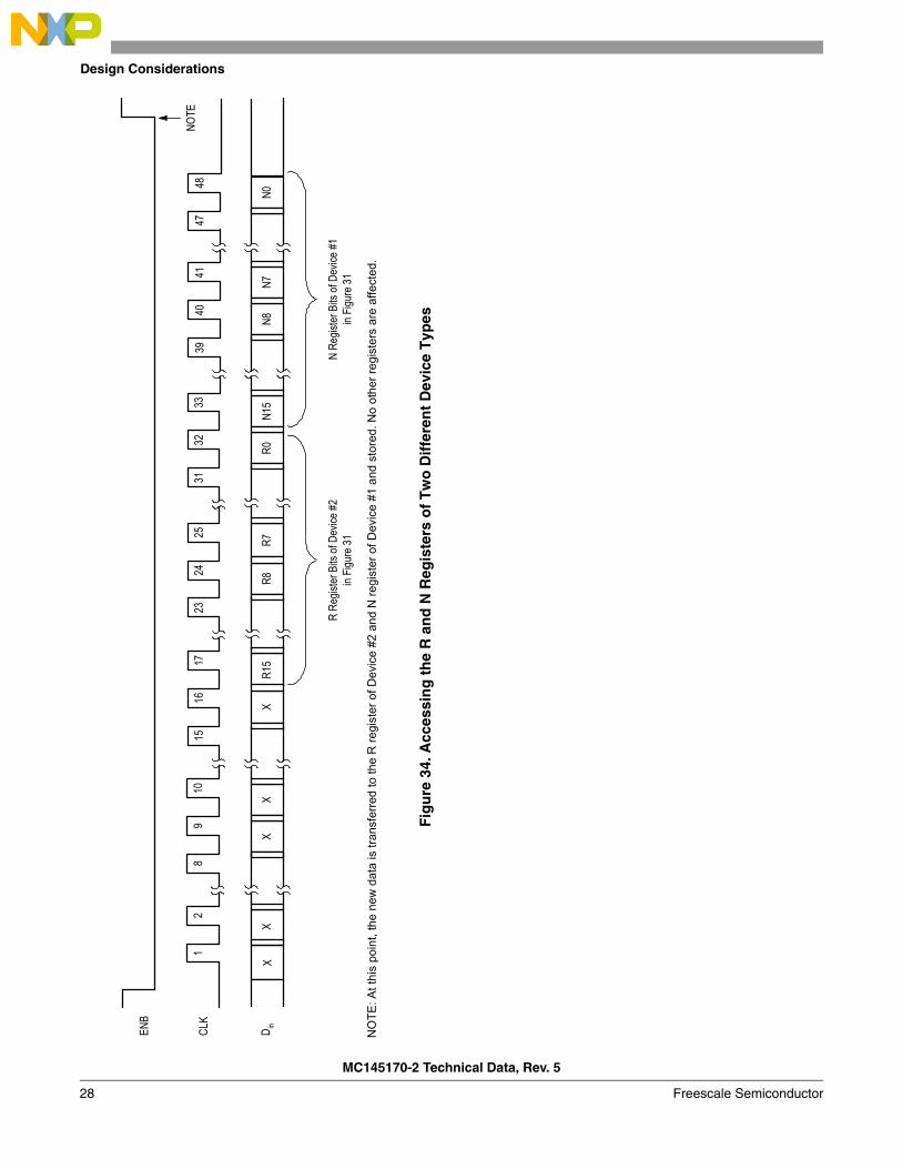
Design Considerations
Fig
ure
34.
Acc
essi
ng
th
e R
an
d N
Reg
iste
rs o
f T
wo
Dif
fere
nt
Dev
ice
Typ
es
NO
TE: A
t thi
s po
int,
the
new
dat
a is
tran
sfer
red
to th
e R
regi
ster
of D
evic
e #2
and
N re
gist
er o
f Dev
ice
#1 a
nd s
tore
d. N
o ot
her r
egis
ters
are
affe
cted
.
12
89
1015
1617
2324
2531
3233
R Re
gister
Bits
of D
evice
#2in
Figur
e 31
N Re
gister
Bits
of D
evice
#1in
Figur
e 31
XX
XX
XR1
5R8
R7R0
N15
3940
4147
48
N8N7
N0
ENB
CLK
D in
NOTE

Packaging
MC145170-2 Technical Data, Rev. 5
Freescale Semiconductor 29
5 Packaging
Figure 35. Outline Dimensions for P Suffix, DIP-16(Case 648-08, Issue R)
Figure 36. Outline Dimensions for D Suffix, SOG-16(Case 751B-05, Issue K)
-A-
B
F C
S
HG
D 16 PL
J
L
M
SEATINGPLANE
1 8
916
K
-T-
MAM0.25 (0.010) T
DIM MIN MAX MIN MAXMILLIMETERSINCHES
A 0.740 0.770 18.80 19.55B 0.250 0.270 6.35 6.85C 0.145 0.175 3.69 4.44D 0.015 0.021 0.39 0.53F 0.040 0.70 1.02 1.77G 0.100 BSC 2.54 BSCH 0.050 BSC 1.27 BSCJ 0.008 0.015 0.21 0.38K 0.110 0.130 2.80 3.30L 0.295 0.305 7.50 7.74M 0 10 0 10S 0.020 0.040 0.51 1.01
____
NOTES:1. DIMENSIONING AND TOLERANCING PER ASME
Y14.5M, 1994.2. CONTROLLING DIMENSION: INCH.3. DIMENSION L TO CENTER OF LEADS WHEN
FORMED PARALLEL.4. DIMENSION B DOES NOT INCLUDE MOLD FLASH.5. ROUNDED CORNERS OPTIONAL.
SEATINGPLANE
0.4916X
BM0.25 AT0.35
1.751.35 0.25
0.10 6
T16X
0.1 T
1.2714X
7°1.250.40
0°
0.250.19
SECTION A-A
NOTES:1. DIMENSIONS ARE IN MILLIMETERS.2. DIMENSIONING AND TOLERANCING PER ASME
Y14.5M, 1994.3. DATUMS A AND B TO BE DETERMINED AT THE PLANE
WHERE THE BOTTOM OF THE LEADS EXIT THE PLASTICBODY.
4. THIS DIMENSION DOES NOT INCLUDE MOLD FLASH,PROTRUSION OR GATE BURRS, MOLD FLASH,PROTRUSIONS OR GATE BURRS SHALL NOT EXCEED0.15 MM PER SIDE. THIS DIMENSION IS DETERMINED ATTHE PLANE WHERE THE BOTTOM OF THE LEADS EXITTHE PLASTIC BODY.
5. THIS DIMENSION DOES NOT INCLUDE INTER-LEAD FLASHOR PROTRUSIONS. INTER-LEAD FLASH ANDPROTRUSIONS SHALL NOT EXCEED 0.25 MM PER SIDE.THIS DIMENSION IS DETERMINED AT THE PLANE WHERETHE BOTTOM OF THE LEADS EXIT THE PLASTIC BODY.
6. THIS DIMENSION DOES NOT INCLUDE DAMBARPROTRUSION. ALLOWABLE DAMBAR PROTRUSION SHALLNOT CAUSE THE LEAD WIDTH TO EXCEED 0.62 MM.
8 9
1 16
8X 6.25.8
M0.25 B
410.09.8
A
4.03.8 B
PIN 1 INDEX
PIN'SNUMBER
AA
5
0.50 X45°0.25

MC145170-2 Technical Data, Rev. 5
30 Freescale Semiconductor
Packaging
Figure 37. Outline Dimensions for DT Suffix, TSSOP-16(Case 948C-03, Issue B)
DIM MIN MAX MIN MAXINCHESMILLIMETERS
A --- 5.10 --- 0.200B 4.30 4.50 0.169 0.177C --- 1.20 --- 0047D 0.05 0.25 0.002 0.010F 0.45 0.55 0.018 0.022G 0.65 BSC 0.026 BSCH 0.22 0.23 0.009 0.010J 0.09 0.24 0.004 0.009
K 0.16 0.32 0.006 0.013
L 6.30 6.50 0.248 0.256M 0 10 0 105 5 5 5
J1 0.09 0.18 0.004 0.007
K1 0.16 0.26 0.006 0.010
A
BPIN 1IDENTIFICATION
L
1 8
916
16x REFK
M0.200 (0.008) T-P-
D
C
SEATINGG H
M0.100 (0.004)
PLANE-T-
-U-
F
M
A
A
KK1
J
J1
SECTION A-A
NOTES:1. DIMENSIONING AND TOLERANCING PER ASME
Y14.5M, 1994.2. CONTROLLING DIMENSION: MILLIMETER.3. DIMENSION A DOES NOT INCLUDE MOLD FLASH,
PROTRUSIONS OR GATE BURRS. MOLD FLASHOR GATE BURRS SHALL NOT EXCEED 0.15(0.006) PER SIDE.
4. DIMENSION B DOES NOT INCLUDE INTERLEADFLASH OR PROTRUSION SHALL NOT EXCEED0.25 (0.010) PER SIDE.
5. DIMENSION K DOES NOT INCLUDE DAMBARPROTRUSION. ALLOWABLE DAMBARPROTRUSION SHALL BE 0.08 (0.003) TOTALEXCESS OF THE K DIMENSION AT MAXIMUMMATERIAL CONDITION.
6. TERMINAL NUMBERS ARE SHOWN FORREFERENCE ONLY.
7. DIMENSIONS A AND B ARE TO BE DETERMINEDAT DATUM PLANE -U-.
MC145170-2 Technical Data, Rev. 5
Freescale Semiconductor 31
NOTES

MC145170-2/DRev. 51/2005
How to Reach Us:
Home Page:www.freescale.com
E-mail:[email protected]
USA/Europe or Locations Not Listed:Freescale SemiconductorTechnical Information Center, CH3701300 N. Alma School Road Chandler, Arizona 85224 +1-800-521-6274 or [email protected]
Europe, Middle East, and Africa:Freescale Halbleiter Deutschland GmbHTechnical Information CenterSchatzbogen 781829 Muenchen, Germany+44 1296 380 456 (English)+46 8 52200080 (English)+49 89 92103 559 (German)+33 1 69 35 48 48 (French)[email protected]
Japan:Freescale Semiconductor Japan Ltd. Headquarters ARCO Tower 15F 1-8-1, Shimo-Meguro, Meguro-ku, Tokyo 153-0064 Japan 0120 191014 or +81 3 5437 [email protected]
Asia/Pacific:Freescale Semiconductor Hong Kong Ltd.Technical Information Center 2 Dai King Street Tai Po Industrial Estate Tai Po, N.T., Hong Kong +800 2666 [email protected]
For Literature Requests Only:Freescale Semiconductor Literature Distribution CenterP.O. Box 5405Denver, Colorado 802171-800-441-2447 or 303-675-2140Fax: [email protected]
Information in this document is provided solely to enable system and software implementers to use Freescale Semiconductor products. There are no express or implied copyright licenses granted hereunder to design or fabricate any integrated circuits or integrated circuits based on the information in this document.
Freescale Semiconductor reserves the right to make changes without further notice to any products herein. Freescale Semiconductor makes no warranty, representation or guarantee regarding the suitability of its products for any particular purpose, nor does Freescale Semiconductor assume any liability arising out of the application or use of any product or circuit, and specifically disclaims any and all liability, including without limitation consequential or incidental damages. Typical parameters that may be provided in Freescale Semiconductor data sheets and/or specifications can and do vary in different applications and actual performance may vary over time. All operating parameters, including Typicals, must be validated for each customer application by customers technical experts. Freescale Semiconductor does not convey any license under its patent rights nor the rights of others. Freescale Semiconductor products are not designed, intended, or authorized for use as components in systems intended for surgical implant into the body, or other applications intended to support or sustain life, or for any other application in which the failure of the Freescale Semiconductor product could create a situation where personal injury or death may occur. Should Buyer purchase or use Freescale Semiconductor products for any such unintended or unauthorized application, Buyer shall indemnify and hold Freescale Semiconductor and its officers, employees, subsidiaries, affiliates, and distributors harmless against all claims, costs, damages, and expenses, and reasonable attorney fees arising out of, directly or indirectly, any claim of personal injury or death associated with such unintended or unauthorized use, even if such claim alleges that Freescale Semiconductor was negligent regarding the design or manufacture of the part.
Freescale and the Freescale logo are trademarks of Freescale Semiconductor, Inc. All other product or service names are the property of their respective owners.© Freescale Semiconductor, Inc. 2005. All rights reserved.
rxzb30
rohstext1