TDC for SeaQuest Wu, Jinyuan Fermilab Jan. 2011 Jan. 2011, Wu Jinyuan, Fermilab [email protected] TDC...
14
TDC for SeaQuest Wu, Jinyuan Fermilab Jan. 2011
-
Upload
stephany-rich -
Category
Documents
-
view
224 -
download
0
Transcript of TDC for SeaQuest Wu, Jinyuan Fermilab Jan. 2011 Jan. 2011, Wu Jinyuan, Fermilab [email protected] TDC...

TDC for SeaQuest
Wu, Jinyuan
Fermilab
Jan. 2011

Jan. 2011, Wu Jinyuan, Fermilab [email protected] TDC for SeaQuest 2
Introduction on FPGA TDC There are two popular schemes for FPGA TDC:
Multiple sampling based scheme: LSB: 0.6 to 1 ns. Delay line based scheme: LSB: 40 to 100 ps.
We are currently working on a variation of the delay line based TDC called Wave Union TDC. Colleagues with requirements of TOF level resolution (< 50 ps) are welcome to contact us.
Jan. 2011, Wu Jinyuan, Fermilab [email protected] TDC for SeaQuest 3
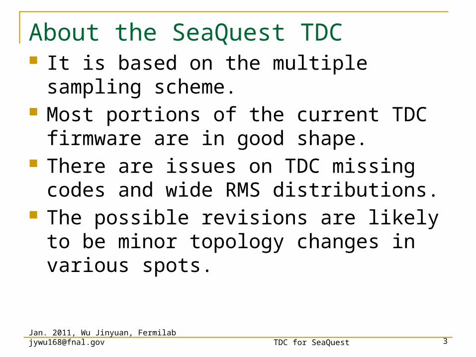
About the SeaQuest TDC It is based on the multiple sampling scheme. Most portions of the current TDC firmware are in
good shape. There are issues on TDC missing codes and wide
RMS distributions. The possible revisions are likely to be minor
topology changes in various spots.

Current Design (sch-chfend.tif)
Jan. 2011, Wu Jinyuan, Fermilab [email protected] TDC for SeaQuest 5
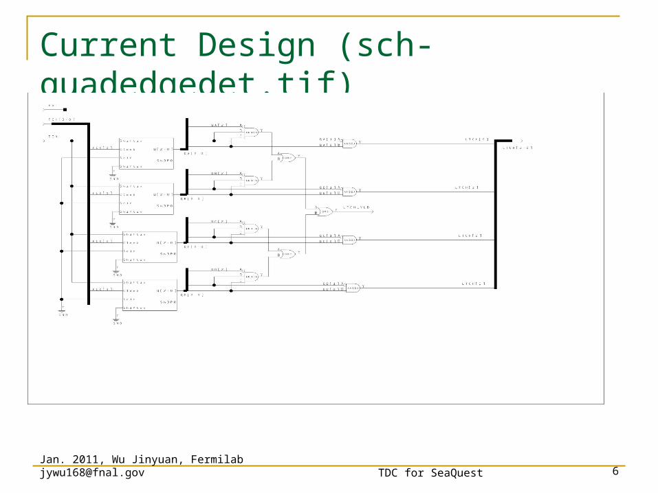
Current Design (sch-quadedgedet.tif)
Jan. 2011, Wu Jinyuan, Fermilab [email protected] TDC for SeaQuest 6

Jan. 2011, Wu Jinyuan, Fermilab [email protected] TDC for SeaQuest 7
Multi-Sampling TDC FPGA c0
c90
c180
c270
c0
MultipleSampling
ClockDomain
Changing
Trans. Detection& Encode
Q0
Q1
Q2
Q3QF
QE
QD
c90
Coarse TimeCounter
DV
T0T1
TS
Ultra low-cost: 48 channels in $18.27 EP2C5Q208C7.
Sampling rate: 360 MHz x4 phases = 1.44 GHz.
LSB = 0.69 ns.
4Ch
Logic elements with non-critical timing are freely placed by the fitter of the compiler.
This picture represent a placement in Cyclone FPGA
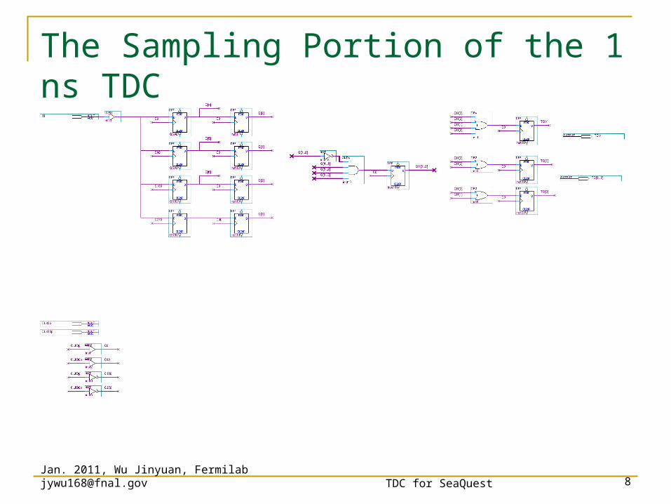
The Sampling Portion of the 1 ns TDC
Jan. 2011, Wu Jinyuan, Fermilab [email protected] TDC for SeaQuest 8

The Simulation of the 1 ns TDC
Jan. 2011, Wu Jinyuan, Fermilab [email protected] TDC for SeaQuest 10

The End
Thanks

Jan. 2011, Wu Jinyuan, Fermilab [email protected] TDC for SeaQuest 12
TDC Using FPGA Logic Chain Delay
This scheme uses current FPGA technology
Low cost chip family can be used. (e.g. EP2C8T144C6 $31.68)
Fine TDC precision can be implemented in slow devices (e.g., 20 ps in a 400 MHz chip).
IN
CLK

Jan. 2011, Wu Jinyuan, Fermilab [email protected] TDC for SeaQuest 13
FPGA TDC A possible choice of the TDC can
be a delay line based architecture called the Wave Union TDC implemented in FPGA.
Shown here is an ASIC-like implementation in a 144-pin device.
18 Channels (16 regular channels + 2 timing reference channels).
This FPGA cost $28, $1.75/channel. (AD9222: $5.06/channel)
LSB ~ 60 ps. RMS resolution < 25 ps. Power consumption 1.3W, or 81
mW/channel. (AD9222: 90 mW/channel)
In
CLK
Wave UnionLauncher A
Jan. 2011, Wu Jinyuan, Fermilab [email protected] TDC for SeaQuest 14
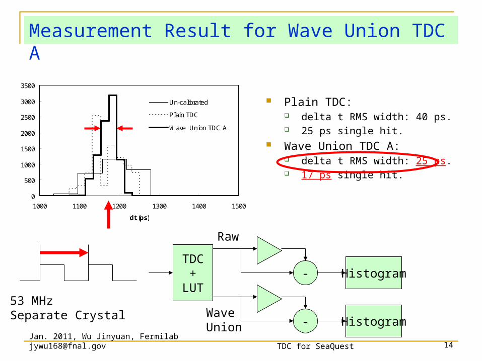
Measurement Result for Wave Union TDC A
Histogram
Raw
TDC+
LUT53 MHzSeparate Crystal
-
-WaveUnion Histogram
Plain TDC: delta t RMS width: 40 ps. 25 ps single hit.
Wave Union TDC A: delta t RMS width: 25 ps. 17 ps single hit.
0
500
1000
1500
2000
2500
3000
3500
1000 1100 1200 1300 1400 1500
dt (ps)
Un-calibrated
Plain TDC
Wave Union TDC A