
tda2320
13
. WIDE SUPPLY VOLTAGE RANGE (3 to 36V) . SINGLE OR SPLIT SUPPLY OPERATION . VERY LOW CURRENT CONSUMPTION (0.8mA) . VERY LOW DISTORTION . NO POP-NOISE N DIP8 (Plastic Package) 1 2 3 4 5 6 7 8 Inverting Input 2 Output 2 Non-inverting Input 2 Output 1 Inverting Input 1 Non-inve rting Input 1 GND CC V - + - + PIN CONNECTIONS (top view) STEREO AMPLIFIER TDA2320A DESCRIPTION The TDA2320A is a stereo class A preamplifier in- tended for application in portable cassette players and high quality audio systems. The TDA2320A is a monolithic integrated circuit in a 8 lead plastic dip. October 1997 ORDER CODES Part Number Temperature Range Package N TDA2320A -40 o C, +105 o C • 1/12
Transcript of tda2320
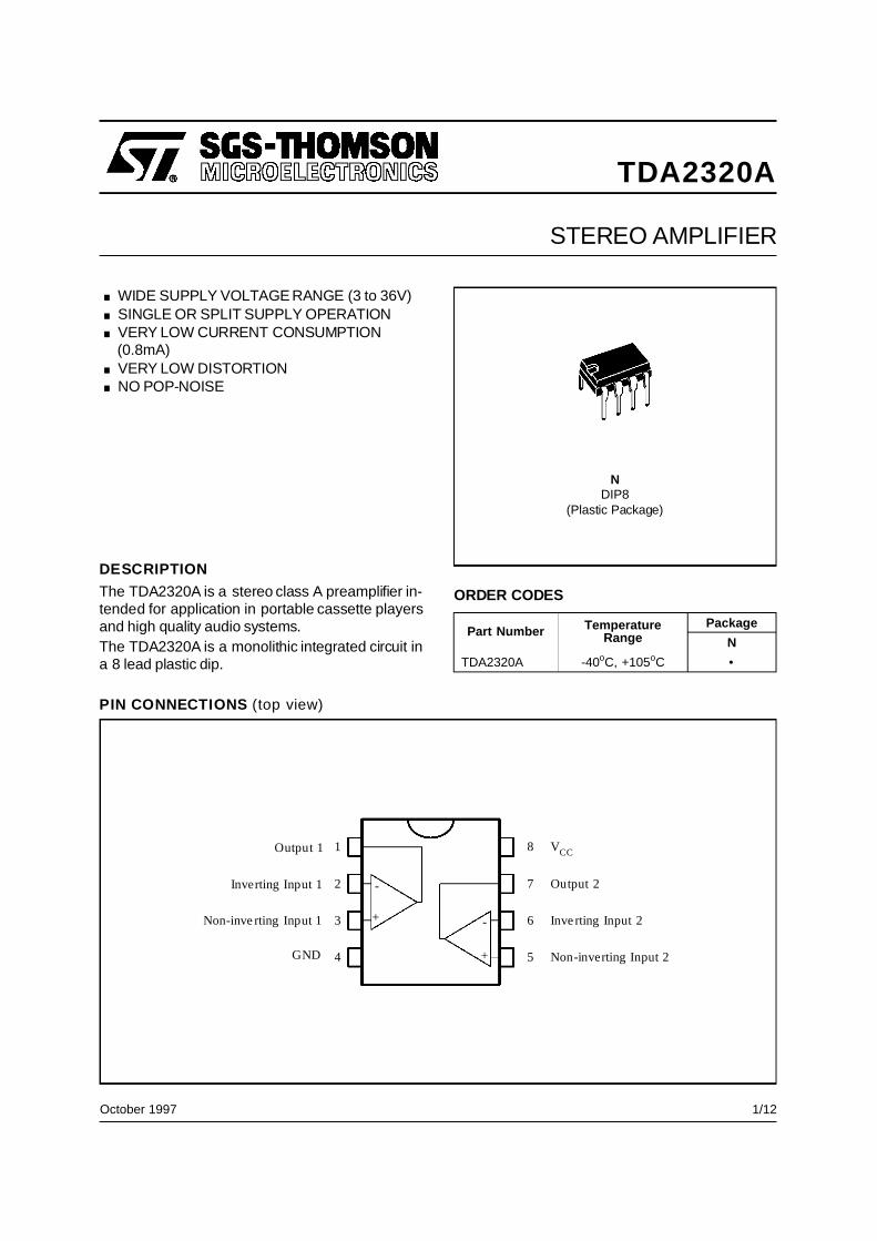
.WIDE SUPPLY VOLTAGE RANGE (3 to 36V). SINGLE OR SPLIT SUPPLY OPERATION.VERY LOW CURRENT CONSUMPTION(0.8mA). VERY LOW DISTORTION.NO POP-NOISE
NDIP8
(Plastic Package)
1
2
3
4 5
6
7
8
Inve rting Input 2
Output 2
Non-inverting Input 2
Output 1
Inverting Input 1
Non-inve rting Input 1
GND
CCV
-
+ -
+
PIN CONNECTIONS (top view)
STEREO AMPLIFIER
TDA2320A
DESCRIPTION
The TDA2320A is a stereo class A preamplifier in-tended for application in portable cassette playersand high quality audio systems.The TDA2320A is a monolithic integrated circuit ina 8 lead plastic dip.
October 1997
ORDER CODES
Part Number TemperatureRange
Package
N
TDA2320A -40oC, +105oC •
1/12
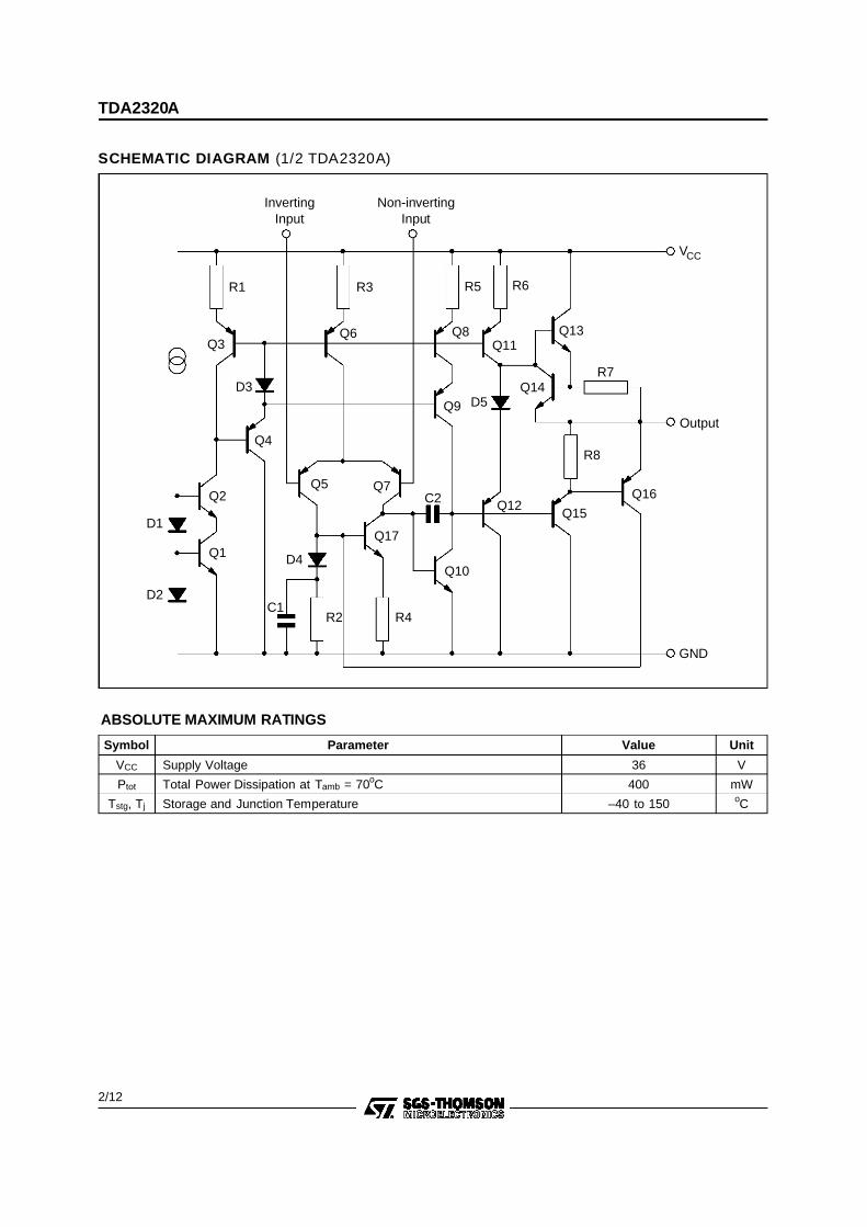
InvertingInput
Non-invertingInput
R1 R3 R5 R6
Q3
D3D5
Q6 Q8Q11
Q13
Q14
Q4
Q9
R7
R8
Q15
Q16Q12
Q17
Q7Q5
D4Q10
R4R2C1
Output
Q2
Q1
D1
D2
C2
VCC
GND
SCHEMATIC DIAGRAM (1/2 TDA2320A)
ABSOLUTE MAXIMUM RATINGS
Symbol Parameter Value Unit
VCC Supply Voltage 36 V
Ptot Total Power Dissipation at Tamb = 70oC 400 mW
Tstg, Tj Storage and Junction Temperature –40 to 150 oC
TDA2320A
2/12

ELECTRICAL CHARACTERISTICSVCC = 15V, Tamb = 25oC (unless otherwise specified) (refer to the test circuits)
Symbol Parameter Min. Typ. Max. UnitVCC Supply Voltage (*) 3 36 VICC Supply Current (*) 0.8 2 mAIib Input Bias Current 150 500 nAVio Input Offset Voltage
Rs ≤ 10kΩ 1 5mV
Iio Input Offset Current 10 50 nAAvd Open Loop Voltage Gain
VCC = 15V f = 333Hzf = 1kHzf = 10kHz
VCC = 4.5V f = 1kHz
80705070
dB
VOPP Output Voltage Swing (f = 1kHz, RL = 600Ω) (*)VCC = 15VVCC = 4.5V
132.5
V
GBP Gain-bandwidth Productf = 20kHz 1.5 2.5
MHz
FBP Power Bandwidth (*)Vo = 5VPP, THD = 1% 40 70
kHz
SR Slew Rate (*) 1 1.6 V/µsTHD Distortion (Vo = 2V, AV = 20dB) (*)
f = 1kHzf = 10kHz
0.030.08
%
en Equivalent Input Noise Voltage (**)Curve A Rs = 50Ω
Rs = 600ΩRs = 5kΩ
B = 22Hz to 22kHz Rs = 50ΩRs = 600ΩRs = 5kΩ
f = 1kHz Rs = 600Ω
11.11.51.31.529
1.4
µV
nV√HzVO1/V02 Channel Separation (**)
f = 1kHz 100dB
SVR Supply Voltage Rejection Ratio(**)f = 100Hz 80
dB
(*) Test circuit of figure 1(**) Test circuit of figure 2
TDA2320A
3/12

1/2TDA2320A
1/2TDA2320A
22µF
18kΩ
82kΩ
4.7µF0.3mV
TAPEHEAD
150Ω
220pF
15kΩ
180kΩ
22µF
18kΩ
10nF
20kΩ
1µF7
85
64
100kΩ
0.1µF
22µF
82kΩ
4.7µF0.3mV
TAPEHEAD
150Ω
220pF
15kΩ
180kΩ
22µF
10nF
20kΩ
1µF1
3
2
100kΩ
VCC
TYPICAL APPLICATION
STEREO PREAMPLIFIER FOR CASSETTE PLAYERS
1/2TDA2320A
22µF 18kΩ
82kΩ
150Ω
220pF
22kΩ
1µF
100kΩ
0.1µF
VCC
0.22µF
IN
OUT
47µF
Rx
TEST CIRCUITS
Figure 1
1/2TDA2320A
33Ω
220pF
0.1µF
0.1µF
OUT
+7.5V
3.3kΩ
-7.5V
R s
Figure 2
TDA2320A
4/12

Figure 3 : Supply Current versus SupplyVoltage
Figure 4 : Supply Current versus AmbientTemperature
Figure 5 : Output Voltage Swing versusLoad Resistance
Figure 6 : Power Bandwidth
Figure 7 : Total Harmonic DistortionversusOutput Voltage
Figure 8 : Total Input Noise versus SourceResistance
TDA2320A
5/12
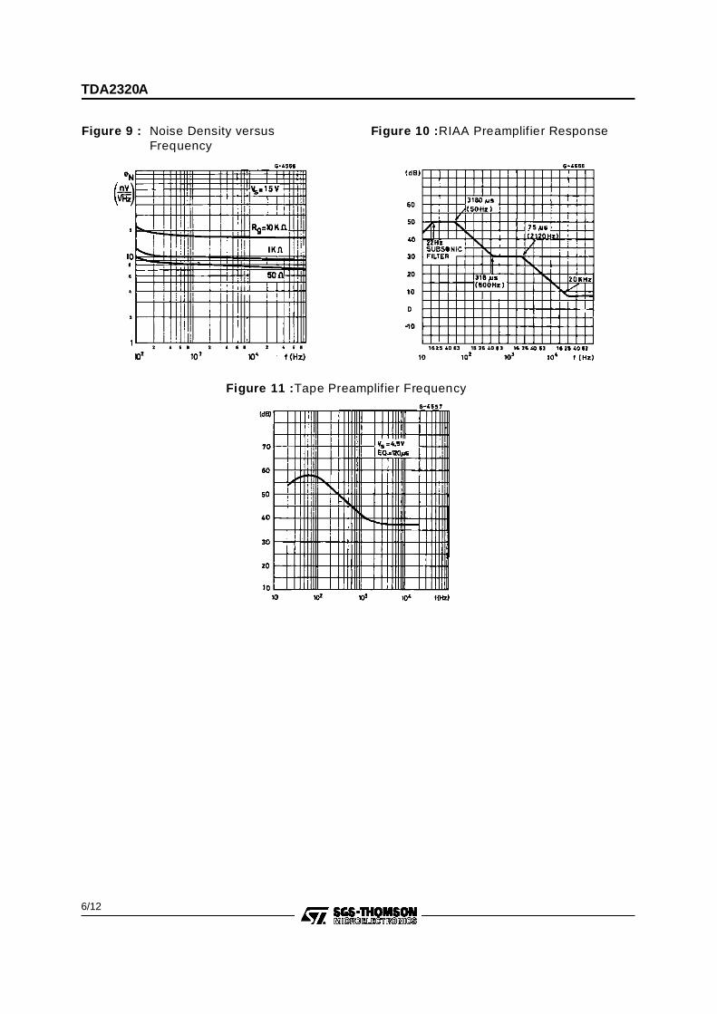
Figure 9 : Noise Density versusFrequency
Figure 10 : RIAA Preamplifier Response
Figure 11 : Tape Preamplifier Frequency
TDA2320A
6/12

1/2TDA2320A
22µF
R518kΩ
R1100kΩ
4.7µF
R7820Ω
100pF
R1022kΩ
10µF
R618kΩ
15nF
1µF78
5
64
R2120kΩ
0.1µFC13C3
C5
IN (L)
+15V
OUT (L)C14
R131kΩ
3.3nFC9
R9220kΩ
C10
C7
1/2TDA2320A
22µF
R3100kΩ
4.7µF
R8820Ω
100pF
R1222kΩ
10µF
15nF
1µF1
3
2
R4120kΩ
C4
C6
IN (R)
OUT (R)C15
R141kΩ
3.3nFC11
R11220kΩ
C12
C8
C1
C2
APPLICATION INFORMATION
Figure 12 : Stereo RIAA Preamplifier
Figure 13 : P.C. Board and Components layout of the Circuit of figure 12
TDA2320A
7/12
1/2TDA2320A
0.22µF
78
5
6
410kΩ 10kΩ
+15V
100nF
5.6nF
-15V
100nF
5.6kΩ
5kΩ
0.47µF
TOWOOFER
AMPLIFIER
1/2TDA2320A
1
3
210kΩ
5.6kΩ
5kΩ
0.1µF
TOTWEETERAMPLIFIER22kΩ
5.6nF 5.6nFIN
12nF
f = 2kHzc
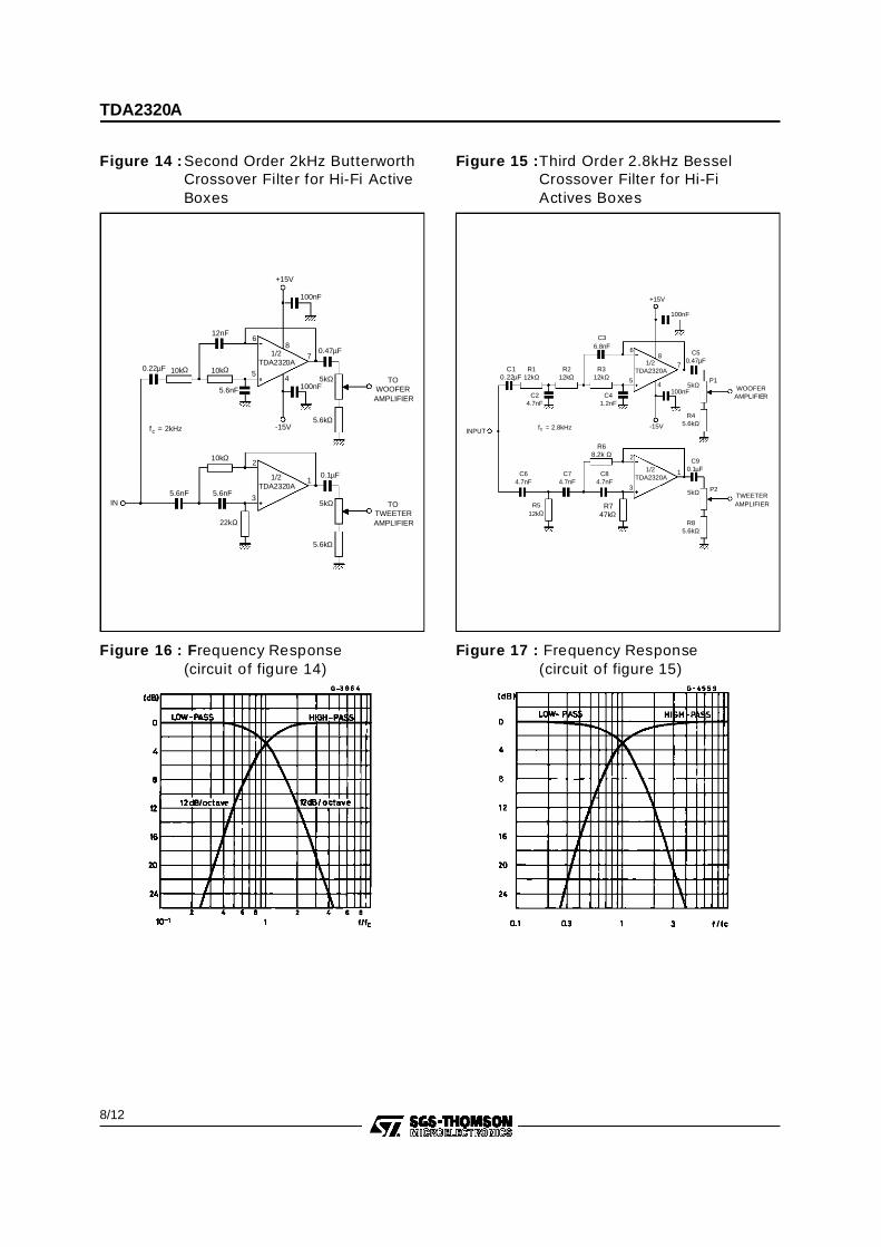
Figure 14 : Second Order 2kHz ButterworthCrossover Filter for Hi-Fi ActiveBoxes
Figure 16 : F requency Response(circuit of figure 14)
1/2TDA2320AC1
0.22µF
78
5
6
4
+15V
100nF
C41.2nF
-15V
100nF
R45.6kΩ
5kΩ
C50.47µF
WOOFERAMPLIFIER
1/2TDA2320A
1
3
2
R68.2k Ω
R85.6kΩ
5kΩ
C90.1µF
TWEETERAMPLIFIERR7
47kΩ
C64.7nF
INPUT
C36.8nF
f = 2.8kHzc
R112kΩ
R212kΩ
C24.7nF
R312kΩ
C74.7nF
R512kΩ
C84.7nF
P1
P2
Figure 15 : Third Order 2.8kHz BesselCrossover Filter for Hi-FiActives Boxes
Figure 17 : Frequency Response(circuit of figure 15)
TDA2320A
8/12

0.3µF
1/2TDA2320A
1
3
210kΩ
22kΩ
IN56nF 56nF
0.1µF
1/2TDA2320A
7
5
6
0.47µF
5kΩ
5.6kΩ
1.8nF
12kΩ12kΩ12kΩ
10nF
VCC
VCC
6.8nF
Figure 18 : 200Hz to 2kHz Active Bandpass Filter for Midrange Speakers
C
-
CVin
22kΩ
10k Ω
1/2TDA2320A
3
2
1Vout
Figure 19 : Subsonic Filter
fc (Hz) C (µF)
15223055100
0.680.470.330.220.1
fc (kHz) C1 (nF) C2 (nF)
351015
3.92.21.2
0.68
6.84.72.21.5
10kΩ
C1
-
C2
Vin
Vout
10kΩ3
2
1/2TDA2320A
1
Figure 20 : High-cut Filter
TDA2320A
9/12

R1
C1
-
R2
C2
C
R
R3
C3
-
R4
C4
1st order 2nd order 3rd order
i
i
1/2TDA2320A
3
2
1
1/2TDA2320A
5
6
7
Figure 21 : Fifth Order 3.4kHz Low-pass Butterworth Filter
C1 = 1.354 .1R
.1
2Π fc= 6.33nF
C1 = 0.421 .1R
.1
2Π fc= 1.97nF
C2 = 1.753 .1R
.1
2Π fc= 8.20nF
C3 = 0.309 .1R
.1
2Π fc= 1.45nF
C4 = 3.325 .1R
.1
2Π fc= 15.14nF
The attenuation of the filter is 30dB at 6.8kHz andbetter than 60dB at 15kHz.
For fc = 3.4kHz and Ri = R1 = R2 = R3 = R4 = 10kΩ, we obtain :
-
10kΩ
3.54nF
10kΩ
60nF
-
10kΩ
16.3nF
10kΩ
220nF
-
10kΩ
86.1nF
10kΩ
161nF
-
0.47µF
56kΩ
2
3
11/2TDA
2320A
6
5
71/2
TDA2320A
2
3
11/2TDA
2320A
6
5
71/2TDA
2320A
Figure 22 : Sixth-pole 355Hz Low-pass Filter (Chebychev type)
This is a6-pole Chebychev type with ±0.25dBripplein the passband.A decouplingstage isused to avoidthe influence of the input impedance of the filter’scharacteristics.
The attenuation is about 55dB at 710Hz andreaches 80dB at 1065Hz. The in band attenuationis limited in practice to the ±0.25dB ripple and doesnot exceed 1/2dB at 0.9fc.
TDA2320A
10/12

1/2TDA2320A OUT
1/2TDA2320A
IN0.22µF
3
2
1
+15V
100nF
56kΩ
-15V
6
4
1.8kΩ 500kΩ
100kΩ
100kΩ3.6kΩ
11kΩ
47nF
47nF
22nF
4.7nF6
5
7
TREBLE1.8kΩ
11kΩMIDRANGE
3.6kΩ
BASS11kΩ
100nF
Figure 23 : Three Band Tone Control
Figure 24 : Frequency Response of theCircuit of figure 23
A : all controls flat
B : bass & treble boost, mid flat
C : bass & treble cut, mid flat
D : mid boost, bass & treble flat
E : mid cut, bass treble flat
TDA2320A
11/12

PM
-DIP
8.E
PS
PACKAGE MECHANICAL DATA8 PINS -PLASTIC DIP
DimensionsMillimeters Inches
Min. Typ. Max. Min. Typ. Max.A 3.32 0.131
a1 0.51 0.020B 1.15 1.65 0.045 0.065b 0.356 0.55 0.014 0.022
b1 0.204 0.304 0.008 0.012
D 10.92 0.430
E 7.95 9.75 0.313 0.384e 2.54 0.100
e3 7.62 0.300e4 7.62 0.300
F 6.6 0260i 5.08 0.200
L 3.18 3.81 0.125 0.150Z 1.52 0.060
DIP
8.T
BL
Information furnished is believed to be accurate and reliable. However, SGS-THOMSON Microelectronics assumes no responsi-bility for the consequences of use of such information nor for any infringement of patents or other rights of third parties whichmay result from its use. No license is granted by implication or otherwise under any patent or patent rights of SGS-THOMSONMicroelectronics. Specifications mentioned in this publ icationare subject to change without notice. This publication supersedesand replaces all information previously supplied. SGS-THOMSON Microelectronics products are not authorized for use as criticalcomponents in life support devices or systems without express written approval of SGS-THOMSON Microelectronics.
1997 SGS-THOMSON Microelectronics – Printed in Italy – All Rights Reserved
SGS-THOMSON Microelectronics GROUP OF COMPANIESAustralia - Brazil - Canada - China - France - Germany - Hong Kong - Italy - Japan - Korea - Malaysia - Malta - Morocco
The Netherlands - Singapore - Spain - Sweden - Switzerland - Taiwan - Thailand - United Kingdo m- U.S.A. OR
DE
RC
OD
E:
TDA2320A
12/12

This datasheet has been download from:
www.datasheetcatalog.com
Datasheets for electronics components.


