TCA 505 BG TCA 505 BG IC for Inductive Proximity Switches with
18
Semiconductor Group 1 TCA 505 BG Besides its basic functions (oscillator, demodulator and threshold switch), the bipolar monolithic IC TCA 505 B includes a number of useful extra functions that enable high-grade, inductive proximity switches to be designed for an attractive price/performance ratio and with space savings. Compared to earlier ICs for inductive proximity switches temperature drift, noise immunity and the switching frequency of the IC have been improved. TCA 505 BG Bipolar IC PG-DSO-16-1 Pb-free lead plating; RoHS compliant Features ● Wide supply voltage of 3.1 to 4.5 V and 4 to 40 V ● Low current consumption of less than 0.8 mA ● Integrated output stage for up to 60 mA output current ● Short-circuit and overload protection of output stages and external components ● Temperature response of the IC compensates that of the coil ● High noise immunity ● High switching frequencies up to 5 kHz ● Useful extra functions ● Suitable for two-wire AC proximity switches ● Temperature range – 40 to 110 ˚C TCA 505 BG Q67000-A8341 PG-DSO-16-1 (SMD) Type Ordering Code Package TCA 505 B Q67000-A8342 Chip IC for Inductive Proximity Switches with Short-Circuit Protection 02.05
Transcript of TCA 505 BG TCA 505 BG IC for Inductive Proximity Switches with
Semiconductor Group 1
TCA 505 BG
Besides its basic functions (oscillator, demodulator and threshold switch), the bipolarmonolithic IC TCA 505 B includes a number of useful extra functions that enable high-grade,inductive proximity switches to be designed for an attractive price/performance ratio and withspace savings.
Compared to earlier ICs for inductive proximity switches temperature drift, noise immunity andthe switching frequency of the IC have been improved.
TCA 505 BG
Bipolar IC
PG-DSO-16-1
Pb-free lead plating; RoHS compliant
Features
Wide supply voltage of 3.1 to 4.5 Vand 4 to 40 V
Low current consumption of less than 0.8 mA Integrated output stage for up to 60 mA
output current Short-circuit and overload protection of output
stages and external components Temperature response of the IC compensates
that of the coil High noise immunity High switching frequencies up to 5 kHz Useful extra functions Suitable for two-wire AC proximity switches Temperature range – 40 to 110 ˚C
TCA 505 BG Q67000-A8341 PG-DSO-16-1 (SMD)
Type Ordering Code Package
TCA 505 B Q67000-A8342 Chip
IC for Inductive Proximity Switcheswith Short-Circuit Protection
02.05
Semiconductor Group 2
TCA 505 BG
TCA 505 BG
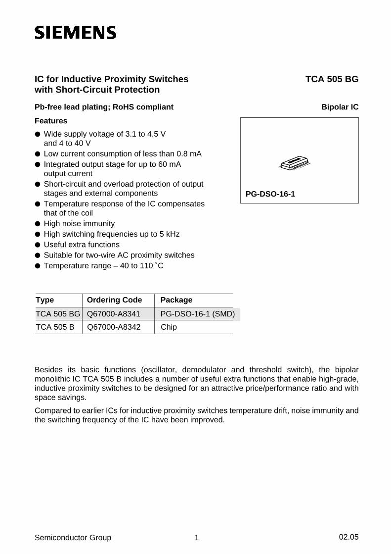
Pin Definitions and Functions
Pin Symbol Function
1 LC Oscillator
2 RDi Distance
3 N.C. Not connected
4 CI Integrating capacitance
5 RHy Hysteresis
6 SC Short-circuit detector
7 GND Ground
8 Q4 Output
9 Q3 Output
10 Q2 Output
11 Q1 Output
12 VS Supply voltage
13 VREF Reference voltage
14 B Base Output Transistors
15 CD Turn-ON delay / Short-circuit delay
16 VT Two-wire regulator
Pin Configurations(top view)
Semiconductor Group 3
TCA 505 BG
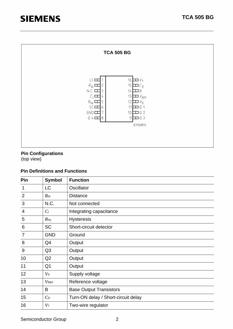
Functional Description and Application
Operation Schematic
Block Diagram
Semiconductor Group 4
TCA 505 BG
Functional Description
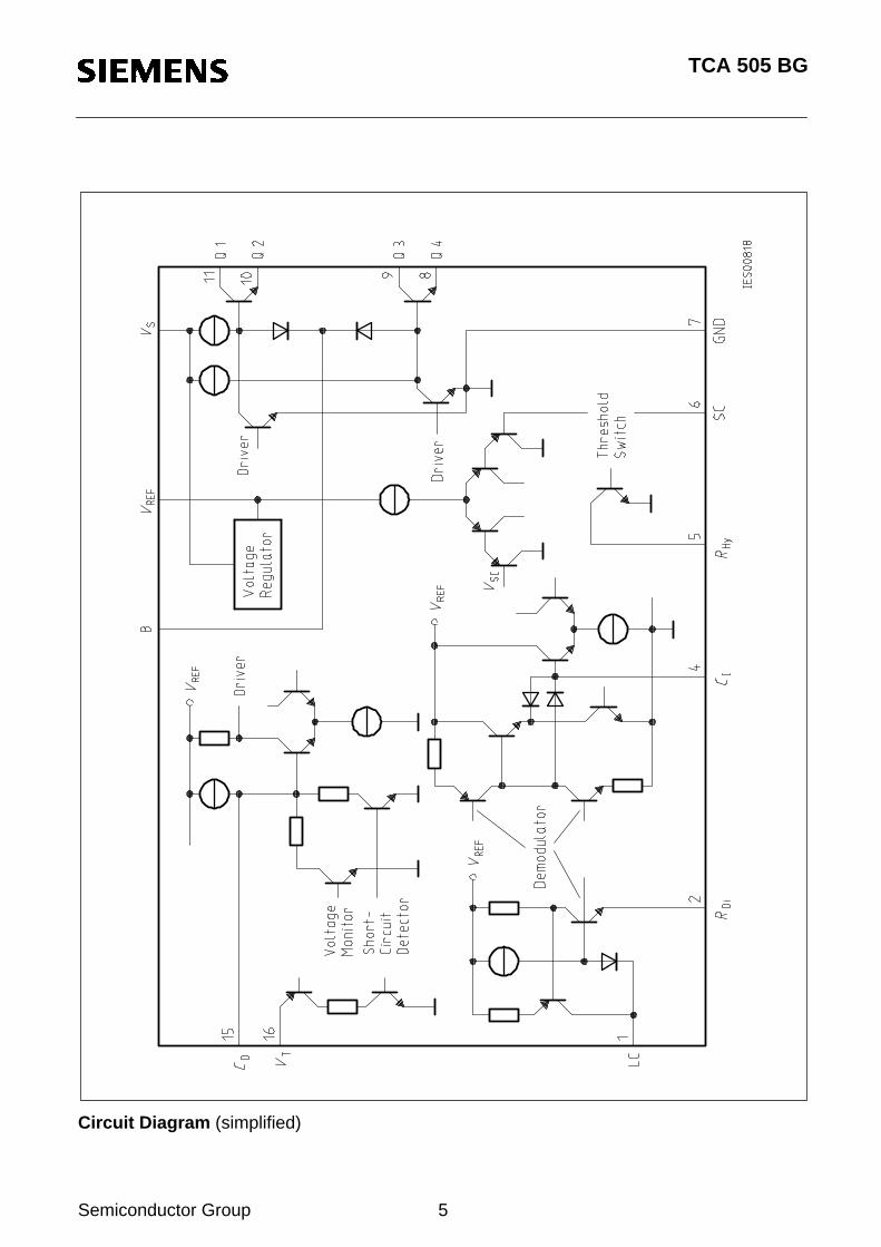
This circuit is used to design inductive proximity switches. The resonant circuit of the LCoscillator is implemented with an open half-pot ferrite and a capacitor in parallel (pin LC). If ametallic target is moved closer to the open side of the half-pot ferrite, energy is drawn from theresonant circuit and the amplitude of the oscillation is reduced accordingly. This change inamplitude is transmitted to a threshold switch by means of a demodulator and triggers theoutputs (see operation schematic ).
By means of an external distance resistor on the oscillator (pin RDi) it is possible to set theswitching distance within wide limits, the optimal distances being 0.1 to 0.6 of the diameter ofthe half-pot ferrite, although both of these parameters can be exceeded. The circuit alsoenables the setting of a path hysteresis by switching of the external distance resistor via pinRHy (see application circuit 1 ).
There are two antiphase output stages (Q1 / Q2 and Q3 / Q4) for max. 50 mA. The outputtransistors are driven in a floating state thus providing the user with optimal flexibility forevaluation of the output signals. It is therefore possible to use the output transistors either asemitter follower, open-collector, as a current source or in push-pull operation. When pin B isconnected to VREF, Q2 and Q4 can be used between 0 V and VREF. The maximum base voltageof the output transistors can be set on pin B. If B is connected to VREF, any constant current upto 50 mA can be set on the outputs by means of resistors on Q2 or Q4 (see applicationcircuits 2 and 3 ).
Q1 through Q4 and also additional external output transistors can be protected againstdestruction by short-circuit or overload. This is the purpose of pin SC which turns off the outputtransistors periodically in the presence of overload.
By means of a capacitor on CD it is possible to set the response delay and the turn-OFF timeof short-circuit protection. The same capacitor also defines the turn-ON delay of the outputstages when the supply voltage is applied, whereby the output stages are inhibited duringbuildup of the oscillator. Finally CD produces a turn-OFF delay of the output stages to preventthe turn-ON delay from running its full length at brief voltage dips on VS.
A switching regulator is incorporated for the voltage supply of the circuit when it is used as atwo-wire AC proximity switch, and this is activated when pin VT is connected to VS. The circuithas a stabilized voltage of approx. 2.9 V that is brought out on pin VREF.
Supply-voltage range: The operating range in normal operation is between 4 and 40 V. If pinVREF is connected to VS, the circuit is operating between 3.1 and 4.5 V. In this case, however,VREF is no longer internally stabilized, i.e. the analog IC functions depend on the operatingvoltage.
Semiconductor Group 5
TCA 505 BG
Circuit Diagram (simplified)
Semiconductor Group 6
TCA 505 BG
Pin Functions
Pin 1; LC
The resonant circuit of the proximity switch is connected between LC and ground.
Pin 2; RDi
A resistor between this pin and ground sets the current in the oscillator circuit. The greater thevalue of the resistor, the smaller is the current feed from the oscillator into the resonant circuitand the greater therefore is the switching distance. The greater the Q of the resonant circuit,the greater is the value of the distance resistor necessary for setting a certain switchingdistance.
Pin 4; CI
CI can remain open; if high noise immunity is to be achieved however, this pin should beprovided with a series RC element (RI, CI). If pin CD is not used, a correctly dimensioned RCelement on this pin will also prevent any erroneous pulses on the output when the supplyvoltage is turned on (see application circuit 1 ).
Pin 5; RHy
Depending on the status of the circuit, RHy will be high-impedance or low-impedance to ground(open collector). If the distance resistance (see RDi) is split into two resistors RDi and RHy, adistance hysteresis can be set by means of RHy. If series hysteresis is applied, RHy is connectedin series with RDi or shorted. If parallel hysteresis is applied, RHy is connected in parallel with RDi
or made high-impedance (see application circuit 1 ).
Pin 6; SC
SC serves for short-circuit sensing in the output circuit that is to be protected. The current canbe sensed referred to ground or VS. The current sensing is made by a dedicated resistor in theoutput circuit. For a voltage drop ≥ 0.3 V across VS and SC or across ground and SC, all outputsare turned off after the turn-OFF delay (brief glitches on the outputs or the charging of linecapacitances therefore do not trigger the short-circuit protection). After a pause about 200times the turn-off delay, the outputs turn-ON again. If the short-circuit is still present, the turn-OFF cycle will start up anew.
Semiconductor Group 7
TCA 505 BG
Both the internal output stages and externally connected output stages can be protectedagainst sustained short-circuits or overload.
A limiting of the output current is an externally connected output stage during the turn-off delaymust be ensured. Normally the current limiting by the β of the output transistor is sufficient,meaning that no further circuit devices are called for (see application circuits ). The outputsQ1 to Q4 are already internally protected against overcurrent so that, in the case of a short-circuit, the current will not exceed 250 mA.
In order to prevent thermal overloads, the current-conducting output is to be connected to pinSC (see application circuit 4 ).
Pins 8, 9, 10, 11; Outputs Q1, Q2, Q3, Q4
Q1 is the open collector, Q2 the open emitter of one output transistor, Q3 the open collectorand Q4 the open emitter of the second output transistor in antiphase with the first outputtransistor (see operation schematic ). Q1 and Q3 or Q2 and Q4 can be connected in parallelas required. The function of the outputs is ensured when the emitter potential of the outputtransistors (Q2, Q4) is between 0 V and the voltage on pin B. If B is not connected, theoperating range of Q2 and Q4 extends to approx. VS – 2 V. For current setting on the outputs,see pin B .
Pin 12; VS
Outputs Q1 through Q4 are inhibited as long as the voltage on VS is below approx. 3.6 V. Theyare enabled between approx. 3.6 and 4 V, the basic function of the circuit is then ensured.During the turn-ON and turn-OFF of VS there are consequently no undesirable static states.The operating data and characteristics apply upwards from 4 V. See pin CD for the avoidanceof erroneous pulses during oscillator buildup.
Pin 13; VREF
The internal stabilized voltage of the IC of approx. 2.9 V appears on this pin. A capacitor canbe connected between VREF and ground to improve the noise immunity of the overall circuitfunction. If VREF is connected to VS, it is possible to operate the circuit in a supply- voltage rangeof 3.1 through 4.5 V. In this case VREF is no longer stabilized. The analog functions of the circuite.g. switching distance, however, are then dependent on the supply voltage.
Semiconductor Group 8
TCA 505 BG
Pin 14; B
This pin serves for limiting the base voltage of the internal output-stage transistors. If this pinis connected to VREF for example, it is possible to set a constant output current (IQ = VREF /external resistor) that is independent of the supply voltage by means of an external resistor
across Q2 (or Q4) and ground (watch out for power dissipation!).
Pin 15; CD
A capacitor on this pin delays the activation of the outputs after the supply voltage is applied(turn-ON delay). In this way erroneous pulses are prevented on the output during buildup ofthe oscillator.
If VS falls to less than 3.6 to 4 V, the outputs are not inhibited until after a turn-OFF delay time,this also being determined by CD. In this way the delayed turn-ON operation described aboveis suppressed if there are just short glitches (voltage dips) on VS. This is of particular advantagefor large core diameters, because in such cases a relativity long turn-ON delay has to beselected and the delayed twin-on operation would otherwise be activated each time there wasa brief voltage dip.
The capacitor CD also sets the turn-off delay and the pause duration in short-circuit operation.The sample / pause ratio is approx. 1:200 (see pin SC ).
If these functions can be dispensed with, CD can remain open.
Pin 16; VT
If this pin is connected to + VS, the supply voltage of the IC (when used as a two-wire proximityswitch) can be generated by switching the outputs. The quiescent current can then be kept low.This mode is primarily suitable for AC switches with power supply by phase-control.
The switching of the outputs is made in a VS range of 6 to 8 V. At 8 V the outputs are turnedon, until VS falls to 6 V. At 6 V the outputs are inhibited, until VS again reaches 8 V. In this modeVS should not exceed 14 V or fall below 4 V.
Semiconductor Group 9
TCA 505 BG
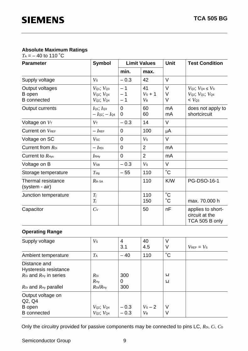
Absolute Maximum RatingsTA = – 40 to 110 ˚C
Parameter Symbol Limit Values Unit Test Condition
Supply voltage VS – 0.3 42 V
Output voltagesB openB connected
VQ1; VQ3
VQ2; VQ4
VQ2; VQ4
– 1– 1– 1
41VS + 1VB
VVV
VQ2; VQ4 ≤ VS
VQ2; VQ1; VQ4
< VQ3
Output currents IQ1; IQ3
– IQ2; – IQ4
00
6060
mAmA
does not apply toshortcircuit
Voltage on VT VT – 0.3 14 V
Current on VREF – IREF 0 100 µA
Voltage on SC VSC 0 VS V
Current from RDi – IRDi 0 2 mA
Current to RHys IRHy 0 2 mA
Voltage on B VSB – 0.3 VS V
Storage temperature Tstg – 55 110 ˚C
Thermal resistance(system - air)
Rth SA 110 K/W PG-DSO-16-1
Junction temperature Tj
Tj
110150
˚C˚C max. 70.000 h
Capacitor CV 50 nF applies to short-circuit at theTCA 505 B only
Operating Range
min. max.
Supply voltage VS 43.1
404.5
VV VREF = VS
Ambient temperature TA – 40 110 ˚C
Distance andHysteresis resistanceRDi and RHy in series
RDi and RHy parallel
RDi
RHy
RDi/RHy
3000300
ΩΩ
Output voltage onQ2, Q4B openB connected
VQ2; VQ4
VQ2; VQ4
– 0.3– 0.3
VS – 2VB
VV
Only the circuitry provided for passive components may be connected to pins LC, RDi, CI, CD
Semiconductor Group 10
TCA 505 BG
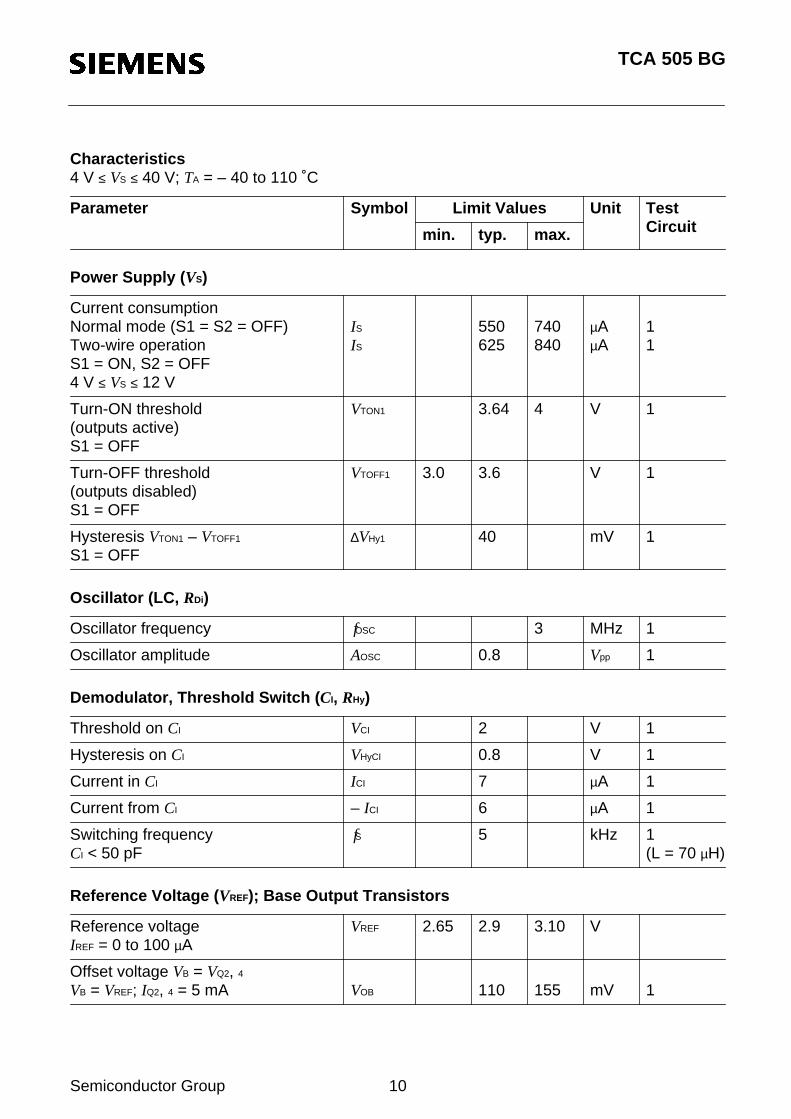
Characteristics4 V ≤ VS ≤ 40 V; TA = – 40 to 110 ˚C
Parameter Symbol
min. typ. max.
Unit TestCircuit
Power Supply ( VS)
Oscillator (LC, RDi)
Demodulator, Threshold Switch ( CI, RHy)
Reference Voltage ( VREF); Base Output Transistors
Current consumptionNormal mode (S1 = S2 = OFF)Two-wire operationS1 = ON, S2 = OFF4 V ≤ VS ≤ 12 V
IS
IS
550625
740840
µAµA
11
Turn-ON threshold(outputs active)S1 = OFF
VTON1 3.64 4 V 1
Turn-OFF threshold(outputs disabled)S1 = OFF
VTOFF1 3.0 3.6 V 1
Hysteresis VTON1 – VTOFF1
S1 = OFF∆VHy1 40 mV 1
Oscillator frequency fOSC 3 MHz 1
Oscillator amplitude AOSC 0.8 Vpp 1
Threshold on CI VCI 2 V 1
Hysteresis on CI VHyCI 0.8 V 1
Current in CI ICI 7 µA 1
Current from CI – ICI 6 µA 1
Switching frequencyCI < 50 pF
fS 5 kHz 1(L = 70 µH)
Reference voltageIREF = 0 to 100 µA
VREF 2.65 2.9 3.10 V
Offset voltage VB = VQ2, 4
VB = VREF; IQ2, 4 = 5 mA VOB 110 155 mV 1
Limit Values
Semiconductor Group 11
TCA 505 BG
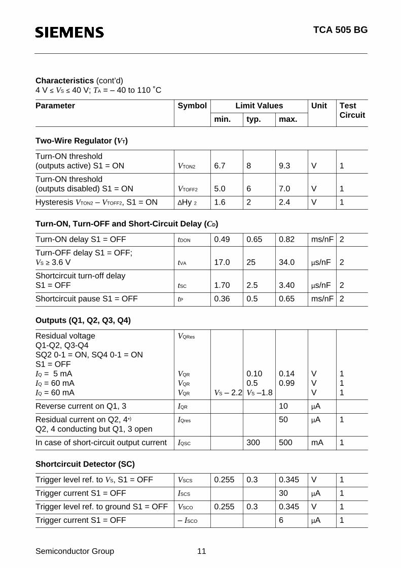
Characteristics (cont’d)4 V ≤ VS ≤ 40 V; TA = – 40 to 110 ˚C
Parameter Symbol
min. typ. max.
Unit TestCircuit
Two-Wire Regulator ( VT)
Limit Values
Turn-ON, Turn-OFF and Short-Circuit Delay ( CD)
Outputs (Q1, Q2, Q3, Q4)
Shortcircuit Detector (SC)
Turn-ON threshold(outputs active) S1 = ON VTON2 6.7 8 9.3 V 1
Turn-ON threshold(outputs disabled) S1 = ON VTOFF2 5.0 6 7.0 V 1
Hysteresis VTON2 – VTOFF2, S1 = ON ∆Hy 2 1.6 2 2.4 V 1
Turn-ON delay S1 = OFF tDON 0.49 0.65 0.82 ms/nF 2
Turn-OFF delay S1 = OFF;VS ≥ 3.6 V tVA 17.0 25 34.0 µs/nF 2
Shortcircuit turn-off delayS1 = OFF tSC 1.70 2.5 3.40 µs/nF 2
Shortcircuit pause S1 = OFF tP 0.36 0.5 0.65 ms/nF 2
Residual voltageQ1-Q2, Q3-Q4SQ2 0-1 = ON, SQ4 0-1 = ONS1 = OFFIQ = 5 mAIQ = 60 mAIQ = 60 mA
VQRes
VQR
VQR
VQR VS – 2.2
0.100.5VS –1.8
0.140.99
VVV
111
Reverse current on Q1, 3 IQR 10 µA
Residual current on Q2, 4*)
Q2, 4 conducting but Q1, 3 openIQres 50 µA 1
In case of short-circuit output current IQSC 300 500 mA 1
Trigger level ref. to VS, S1 = OFF VSCS 0.255 0.3 0.345 V 1
Trigger current S1 = OFF ISCS 30 µA 1
Trigger level ref. to ground S1 = OFF VSCO 0.255 0.3 0.345 V 1
Trigger current S1 = OFF – ISCO 6 µA 1
Semiconductor Group 12
TCA 505 BG
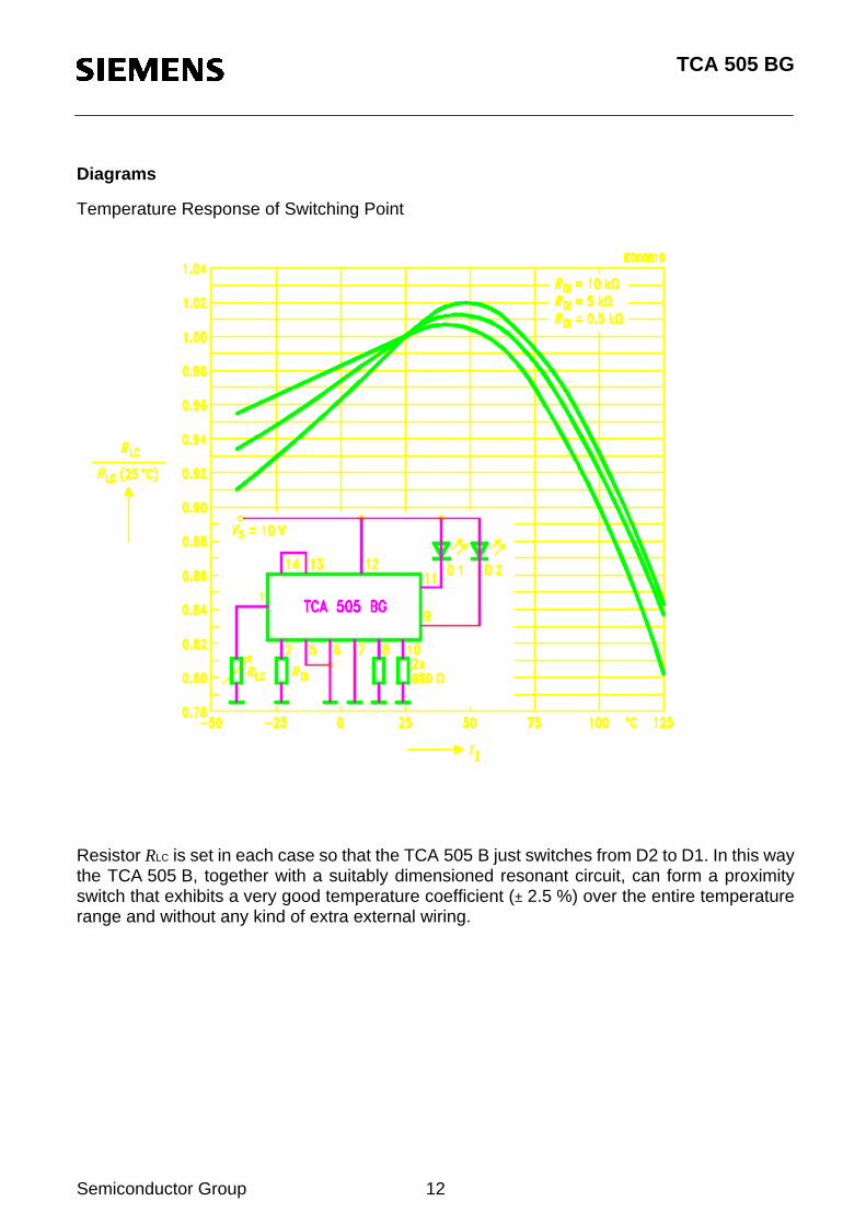
Diagrams
Temperature Response of Switching Point
Resistor RLC is set in each case so that the TCA 505 B just switches from D2 to D1. In this waythe TCA 505 B, together with a suitably dimensioned resonant circuit, can form a proximityswitch that exhibits a very good temperature coefficient (± 2.5 %) over the entire temperaturerange and without any kind of extra external wiring.
Semiconductor Group 13
TCA 505 BG
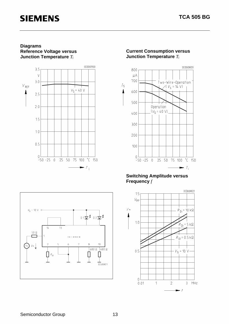
DiagramsReference Voltage versusJunction Temperature Tj
Current Consumption versusJunction Temperature Tj
Switching Amplitude versusFrequency f
Semiconductor Group 14
TCA 505 BG
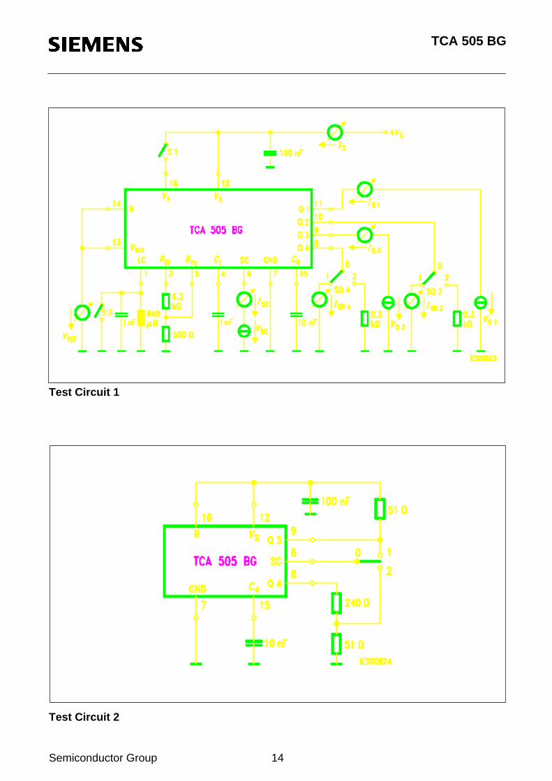
Test Circuit 1
Test Circuit 2
Semiconductor Group 15
TCA 505 BG
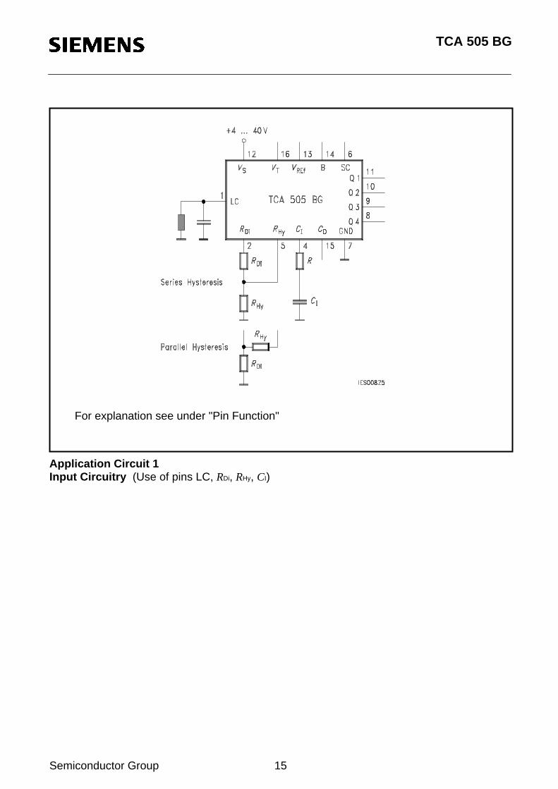
Application Circuit 1Input Circuitry (Use of pins LC, RDi, RHy, CI)
For explanation see under "Pin Function"
Semiconductor Group 16
TCA 505 BG
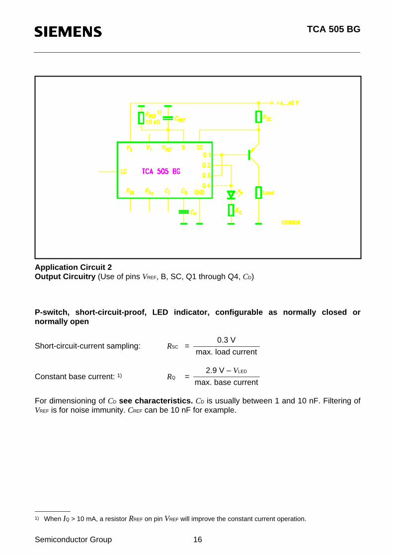
Application Circuit 2Output Circuitry (Use of pins VREF, B, SC, Q1 through Q4, CD)
P-switch, short-circuit-proof, LED indicator, configurable as normally closed ornormally open
For dimensioning of CD see characteristics. CD is usually between 1 and 10 nF. Filtering ofVREF is for noise immunity. CREF can be 10 nF for example.
Short-circuit-current sampling: RSC =
Constant base current: 1) RQ =
0.3 V
max. load current
2.9 V – VLED
max. base current
1) When IQ > 10 mA, a resistor RREF on pin VREF will improve the constant current operation.
Semiconductor Group 17
TCA 505 BG
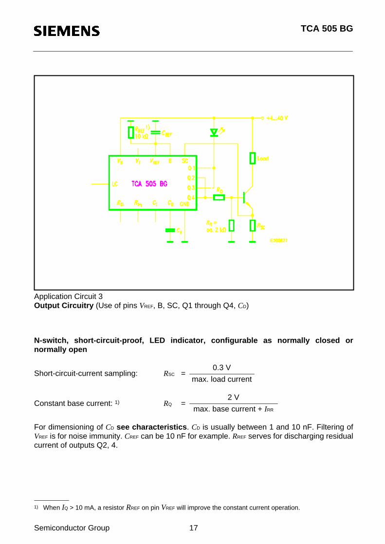
Application Circuit 3Output Circuitry (Use of pins VREF, B, SC, Q1 through Q4, CD)
N-switch, short-circuit-proof, LED indicator, configurable as normally closed ornormally open
For dimensioning of CD see characteristics . CD is usually between 1 and 10 nF. Filtering ofVREF is for noise immunity. CREF can be 10 nF for example. RREF serves for discharging residualcurrent of outputs Q2, 4.
Short-circuit-current sampling: RSC =
Constant base current: 1) RQ =
0.3 V
max. load current
2 V
max. base current + IRR
1) When IQ > 10 mA, a resistor RREF on pin VREF will improve the constant current operation.
Semiconductor Group 18
TCA 505 BG
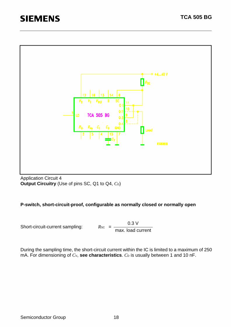
Application Circuit 4Output Circuitry (Use of pins SC, Q1 to Q4, CD)
P-switch, short-circuit-proof, configurable as normally closed or normally open
During the sampling time, the short-circuit current within the IC is limited to a maximum of 250mA. For dimensioning of CV, see characteristics . CD is usually between 1 and 10 nF.
Short-circuit-current sampling: RSC =0.3 V
max. load current