Tapa Ghosh Vathys a (Single) Chip Vathys: Petascale...
28
Vathys: Petascale Deep Learning on a (Single) Chip Tapa Ghosh Vathys
Transcript of Tapa Ghosh Vathys a (Single) Chip Vathys: Petascale...
Vathys: Petascale Deep Learning on a (Single) Chip
Tapa GhoshVathys

What is deep learning?In a sentence: Layers of parametric, differentiable operations whose parameters are changed using gradient information.
Below is a Convolutional Neural Network, one of the most commonly used type ( along with LSTMs)
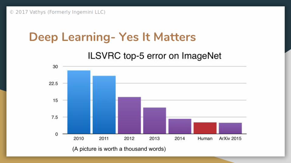
Deep Learning- Yes It Matters
(A picture is worth a thousand words)

Vision: Deep Learning Supercomputing on a Chip (“SoC”)Ideal is 1 PetaFLOP of compute (fp8/fp16) in a TDP similar to the Volta.
And not only that, we want it to be an usable PetaFLOP, we don’t want to
advertise something like 120 TFLOPs peak but get much less in the real world.
And of course, we need to find a way to feed these compute units with
enough bandwidth.
Aggregate compute should not be measured in petaflops while memory
bandwidth is measured in gigabytes.
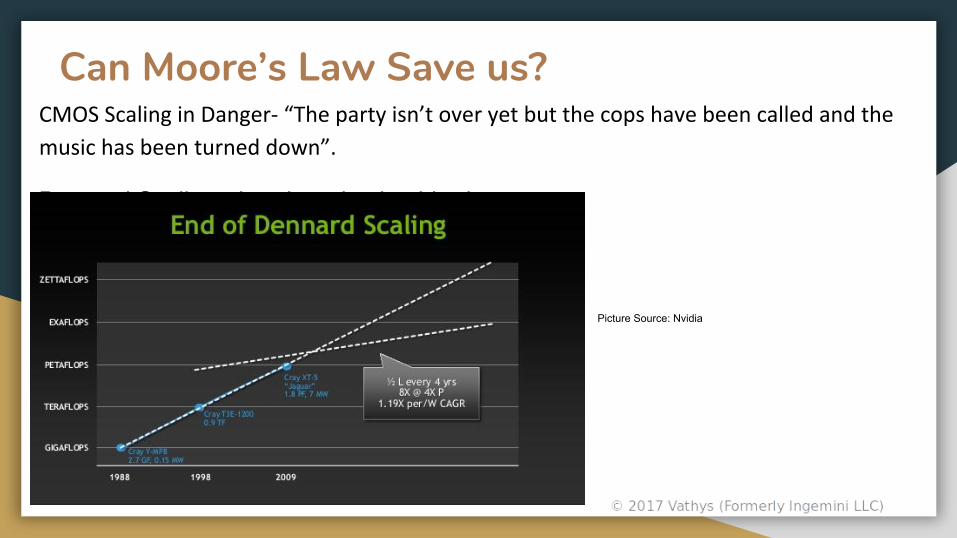
Can Moore’s Law Save us?CMOS Scaling in Danger- “The party isn’t over yet but the cops have been called and the
music has been turned down”.
Dennard Scaling already on its deathbed.
Picture Source: Nvidia
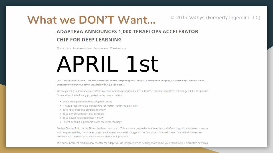
What we DON’T Want...
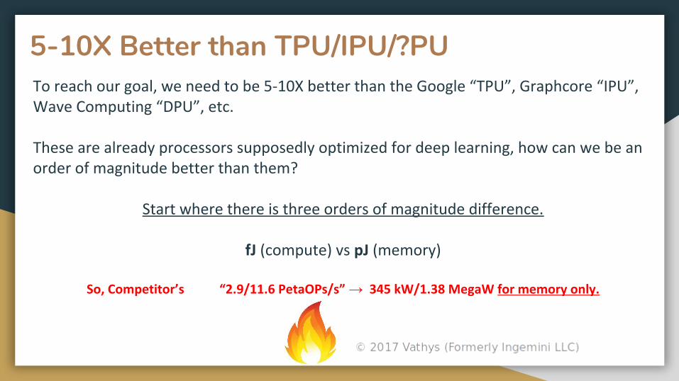
5-10X Better than TPU/IPU/?PUTo reach our goal, we need to be 5-10X better than the Google “TPU”, Graphcore “IPU”, Wave Computing “DPU”, etc.
These are already processors supposedly optimized for deep learning, how can we be an order of magnitude better than them?
Start where there is three orders of magnitude difference.
fJ (compute) vs pJ (memory)
So, Competitor’s “2.9/11.6 PetaOPs/s” → 345 kW/1.38 MegaW for memory only.
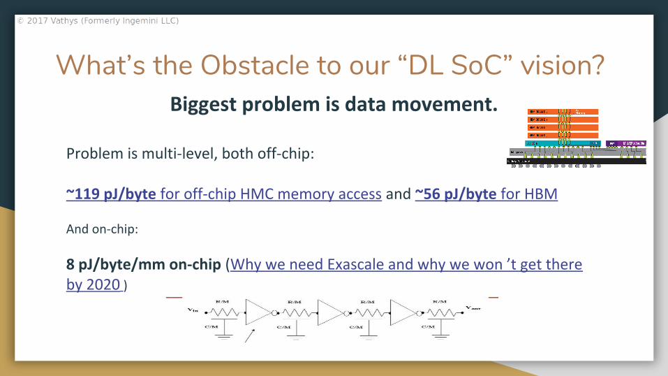
What’s the Obstacle to our “DL SoC” vision?Biggest problem is data movement.
Problem is multi-level, both off-chip:
~119 pJ/byte for off-chip HMC memory access and ~56 pJ/byte for HBM
And on-chip:
8 pJ/byte/mm on-chip (Why we need Exascale and why we won ’t get there by 2020 )
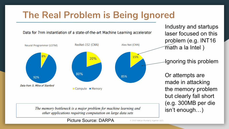
The Real Problem is Being IgnoredIndustry and startups laser focused on this problem (e.g. INT16 math a la Intel )
Ignoring this problem
Or attempts are made in attacking the memory problem but clearly fall short (e.g. 300MB per die isn’t enough…)
Picture Source: DARPA

Hierarchical Approach
Architecture
Circuit Level
Device Level

Architecture Level Innovations● Optimized to reduce data movement
- ~50 um between compute stages (repeaterless!)
● Dataflow (“dataflow-only”) architecture: more suitable for DL
computations than control flow architecture used by competitors.
● True dataflow, at both high/low level, not control flow + data flow.
● Novel data use optimizations for key operations (e.g. convolutions) ahead
of the literature.
● “Tensor native” memory architecture- address large pieces of memory at
once. Less work for address decoder, easier to get bandwidth and I/O and
allows for novel bitline hierarchy techniques.
● Pipelining to expose parallelism, not batches.
One DLE has all the memory it needs, no external memory needed.
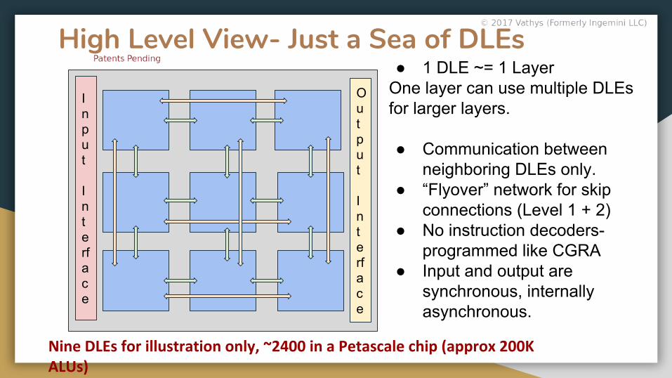
High Level View- Just a Sea of DLEs● 1 DLE ~= 1 Layer
One layer can use multiple DLEs for larger layers.
● Communication between neighboring DLEs only.
● “Flyover” network for skip connections (Level 1 + 2)
● No instruction decoders- programmed like CGRA
● Input and output are synchronous, internally asynchronous.
Input
Interface
Output Interface
Nine DLEs for illustration only, ~2400 in a Petascale chip (approx 200K ALUs)

DLE Block Diagram
Activation Memory (Tensor and tensor slice addressable)
Weight Memory (tensor slice addressable)
Activation Buffer(s)
Writeback Buffer(s)
Convolution/MatMul Pipeline
SIMD CUsSIMD CUs
SIMD CUs SIMD CUs
Activation + Normalization Units
NoC
NoCNoC
NoC
SIMD CUs
SIMD CUs

Circuit Level Innovation● Underappreciated source of “data movement” is in clock lines.
- Up to ~60% of total power (Prof. Dally: Exascale Challenges)
● New form of asynchronous logic:
- 10% overhead compared to 2X+ for previous SOTA.
- Functionality immune to process variations
- Higher performance and no guardbanding necessary
- True asynchronous logic (not GALS like some competitors)
- ~12 “GHz” effective and sustainable “clock” rate (measured on 28nm).
- ~45.2ps delay and ~6 fJ energy at 0.7v supply for 4-bit ALU, deeply pipelined to 8-bit multiply and 16-bit accumulate.
- Memory access hyper-pipelined with dynamic logic in sense amps.
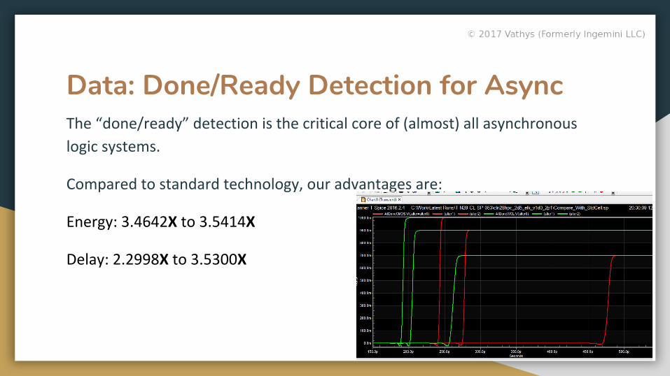
Data: Done/Ready Detection for AsyncThe “done/ready” detection is the critical core of (almost) all asynchronous
logic systems.
Compared to standard technology, our advantages are:
Energy: 3.4642X to 3.5414X
Delay: 2.2998X to 3.5300X

Memory CellWe can get huge advantages by putting all our memory on die. -Unfortunately, impossible with standard 6T SRAM today.
Any feasible new memory must be CMOS compatible.No new materials and no changes to the process (e.g. no litho steps)
Our memory cell is just that, “zero-change” to the process itself:
5X OR (with multilevel) 10X denser than the standard 6T SRAM, 6X to 12X (w/multilevel) lower leakage per bit than standard 6T SRAM.
TCAD simulations complete (promising for multilevel) and MPW in January for silicon validation.

3D Stacking- the Wireless WayPower Speed Area
~7.9 fJ/bit ~40 GBits/S
~9 um^2
Area underneath CAN be used.
No ESD protection needed for these data links.
Cross-talk removed by spacing and/or multiplexing.
Source: SPICE Simulation*
*Waveform

Maximum Achievable Bandwidth per mm^2TSVs: 400 GBits/S @ ~110 fJ/bit Source (slide 23) (But no logic underneath!)
Inductor coils: 800 GBit/S @ ~110 fJ/bit Source(We get logic underneath though!)
Wireless link: 10,000 GBit/S @ ~8 fJ/bit We get logic underneath too! Can be made higher with multiplexing.
Image source: ThruChip

3D Stacking: The Thermal Wall● 3D stacking is limited today by
thermal constraints.● Stacking two dice in the ~300W
TDP regime is impractical, limiting the usefulness of 3D stacking.
Observations from FEM analysis: ● Heat is concentrated in the center
in homogeneous dice as the escape of the sides aren’t there.
● Compute regions are hotspots- do worse when a die is on top.
Source: SemiWiki
Source:SemiEngineering

3D Stacking: Tackling the Thermal WallExploit observations from FEM analysis: Heat “Gaussians” around hotspots:● Thermal density of memory regions of dice is less than the thermal density of
compute regions.→ Place memory regions on top of each other.
“Thermal Multiplexing”: Regions on top of each other work via space-time multiplexing.
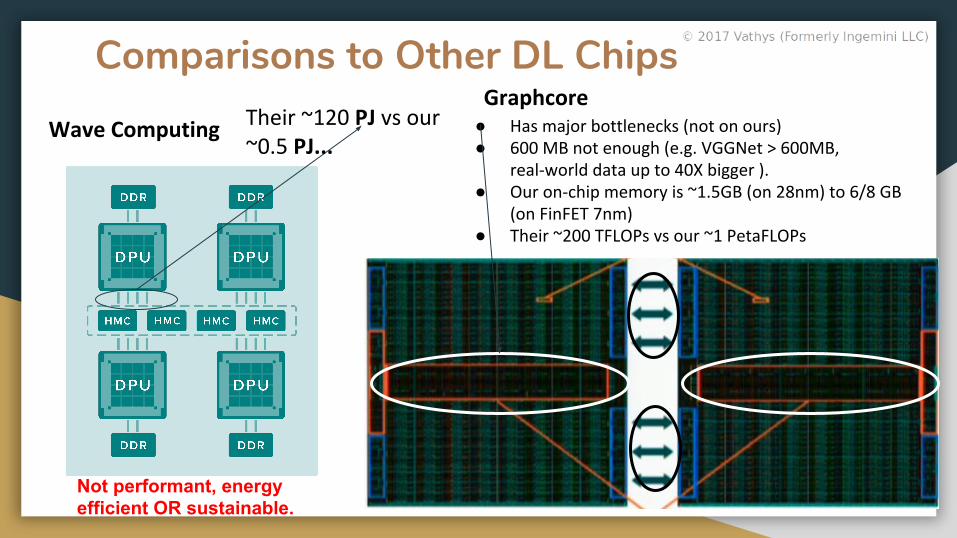
Comparisons to Other DL Chips
Wave Computing Their ~120 PJ vs our ~0.5 PJ...
Graphcore● Has major bottlenecks (not on ours)● 600 MB not enough (e.g. VGGNet > 600MB,
real-world data up to 40X bigger ).● Our on-chip memory is ~1.5GB (on 28nm) to 6/8 GB
(on FinFET 7nm)● Their ~200 TFLOPs vs our ~1 PetaFLOPs
Not performant, energy efficient OR sustainable.
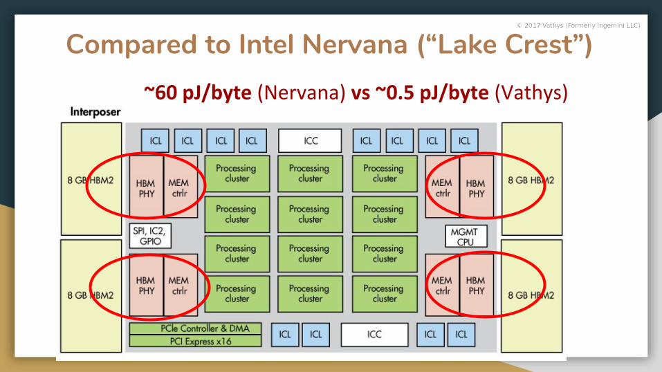
Compared to Intel Nervana (“Lake Crest”)~60 pJ/byte (Nervana) vs ~0.5 pJ/byte (Vathys)

Compared to the TPU v1 A lot of on-chip data movement with an unified memory.
Also, must “lower” convolutions to a matmul, problematic for convolutions.
Image courtesy of Google of course.
Move 8-bits 1mm On-Chip (on 10nm)
~8 pJ
DRAM access 640pJ!!!

Compared to TPU v2
No programmability : (
~60 pJ/byte (TPU v2) vs ~0.5 pJ/byte (Vathys)

Compared to the “Analog Alternative”
● Number of problems with analog computation, even for DL.● Current approaches are flash memory based● Requires power and area intensive ADCs and DACs● Does not solve the data movement problem (in fact makes it worse)
● Huge endurance problem for flash memory (~10^6 max cycles)■ At “1 GHz” will die in ~1 millisecond
● Flash memory is intrinsically unscalable to lower geometries due to leakage difficulties, low number of carriers in the floating gate.
● And of course…. No evidence it can actually retain accuracy...

The Software Stack (aka “How do I actually use it?”)Framework: TensorFlow, Torch, etc.
Computational Graph IR (e.g. ONNX)
DNN-cc Graph Compiler
Vathys Chip Data scientist sees no difference except 10X faster
than TPU, IPU, DPU etc.
Vathys chip is a drop-in replacement
for nVidia GPU.

Timeline (aka “I want one, when can I buy one?”)1. MPW going out in January 2018 to silicon validate 3D stacking and
memory cell.
2. Engineering samples in Q2 2018, funding contingent.
3. Production shipping in Q3 2018, funding contingent.
4. Production shipping on 7nm in Q1 2019, also funding contingent.

Thank you!
Any questions?


![Computational Insights and the Theory of Evolutionweb.stanford.edu/class/ee380/Abstracts/120425-slides.pdfBefore Darwin • Charles Babbage [Paraphrased] “God created not species,](https://static.fdocuments.us/doc/165x107/5f16f2cd0844e33b5013cf7e/computational-insights-and-the-theory-of-before-darwin-a-charles-babbage-paraphrased.jpg)