T2 Analog I-O Modules
88
UM-TS02∗∗∗-E026 PROGRAMMABLE CONTROLLER PROSEC T2-series ANALOG I/O MODULES AD268 / DA264 / TC218 USER’S MANUAL TOSHIBA CORPORATION
Transcript of T2 Analog I-O Modules

8/8/2019 T2 Analog I-O Modules
http://slidepdf.com/reader/full/t2-analog-i-o-modules 1/88
UM-TS02∗∗∗-E026
PROGRAMMABLE CONTROLLER
PROSEC T2-series
ANALOG I/O MODULES
AD268 / DA264 / TC218
USER’S MANUAL
TOSHIBA CORPORATION

8/8/2019 T2 Analog I-O Modules
http://slidepdf.com/reader/full/t2-analog-i-o-modules 2/88
Important Information
Misuse of this equipment can result in property damage or human injury.Because controlled system applications vary widely, you should satisfy yourselfas to the acceptability of this equipment for your intended purpose.In no event will Toshiba Corporation be responsible or l iable for either indirector consequential damage or injury that may result from the use of this equipment.
No patent liability is assumed by Toshiba Corporation with respect to use ofinformation, illustrations, circuits, equipment or examples of application in thispublication.
Toshiba Corporation reserves the right to make changes and improvements to thispublication and/or related products at any time without notice. No obligation shall be
incurred other than as noted in this publication.
This publication is copyrighted and contains proprietary material. No part of this bookmay be reproduced, stored in a retrieval system, or transmitted, in any form or by any
means electrical, mechanical, photocopying, recording, or otherwise withoutobtaining prior written permission from Toshiba Corporation.
© TOSHIBA Corporation 2001, All rights reserved
Publication number: UM-TS02∗∗∗-E026
1st edition December 2001, 2nd edition September 2002

8/8/2019 T2 Analog I-O Modules
http://slidepdf.com/reader/full/t2-analog-i-o-modules 3/88
User’s Manual 1
Safety Precautions
The AD268, DA264, and TC218 are the analog input/output modules for Toshiba’s ProgrammableController PROSEC T2-series (T2/T2E/T2N).Read this manual thoroughly before using this module. Also, keep this manual and related manualsso that you can read them anytime while this module is in operation.
Safety Symbols
The following safety symbols are used on the product and/or in the related manuals.Pay attention to the information preceded by the following symbols for safety.
! WARNING
! CAUTION
Safety Precautions
! CAUTION
• Turn off power to the PLC (T2, T2E or T2N) and to this module (AD268, DA264 or TC218)before removing or mounting this module. Failure to do so can cause electrical shock ordamage to this product.
• Read the Safety Precautions described in the T2, T2E or T2N User’s Manual before usingthis module.
• Follow the instructions described in this manual and in the T2, T2E or T2N User’s Manualwhen installing and wiring this module.
• This module has been designed for the T2/T2E/T2N. Use your AD268/DA264/TC218 onlyon the T2-series PLC rack.
• These modules consume the internal 5 Vdc power as shown below.AD268 ... 300 mADA264 ... 230 mATC218 ... 300 mA
Confirm that the total 5 Vdc consumed current per one power supply module is within thelimit (2.5 A). If it exceeds the limit, the T2/T2E/T2N cannot operate properly and this maycause unsafe situation.
Indicates a potentially hazardous situation which, if not avoided, couldresult in death or serious injury.
Indicates a potentially hazardous situation which, if not avoided, mayresult in minor or moderate injury. It may also be used to alert againstunsafe practices.

8/8/2019 T2 Analog I-O Modules
http://slidepdf.com/reader/full/t2-analog-i-o-modules 4/88
2 Analog I/O Modules (AD268 / DA264 / TC218)
About This Manual
About This Manual
This manual describes the specification and the operations of Toshiba's analog I/O modules(AD268, DA264 and TC218) for PROSEC T2 series programmable controllers.Read this manual carefully for your correct operation of these modules.
This manual consists in three parts.
Part 1 ... 8 channel analog input module AD268Part 2 ... 4 channel analog output module DA264Part 3 ... 8 channel thermocouple input module TC218
Related Manual
The following related manuals are available for your reference.
T2E User's Manual (UM-TS02E∗∗∗∗∗∗∗∗-E001)This manual describes the configuration, specification, installation, wiring, and maintenance ofthe basic hardware of the programmable controller T2E.The functions of the T2E and how to use them, and the information necessary for creating userprogram are also described.
T2N User's Manual (UM-TS02N∗∗∗∗∗∗∗∗ -E001)This manual describes the configuration, specification, installation, wiring, and maintenance of
the basic hardware of the programmable controller T2N.The functions of the T2N and how to use them, and the information necessary for creating userprogram are also described.
T-series Instruction Set (UM-TS03∗∗∗∗∗∗∗∗∗∗∗∗ -E004)This manual describes the detailed specifications of instructions for Toshiba's T-seriesprogrammable controllers.
Note: In this manual, the T2 series programmable controllers (T2, T2E, and T2N) are called asT2 for ease of explanation.

8/8/2019 T2 Analog I-O Modules
http://slidepdf.com/reader/full/t2-analog-i-o-modules 5/88
User’s Manual 3
Table of Contents
Table of Contents
Safety Precautions ............................................................................................................ 1
About This Manual ............................................................................................................ 2
Part 1 8 Channel Analog Input Module AD268
1. Introduction …………….……………………………………………………………….… 8
1.1 AD268 functions ............………………..…………………….………………………… 81.2 External features …......…………………………………………………………………. 9
2. Specifications ….………………………………………………………………………... 10
2.1 Specifications .................…………….……………………………………………….. 102.2 Internal block diagram ………….......………………………………………………… 11
3. Input Type Setting ….........……………………………………………………………... 12
3.1 Jumper plug setting ........…………….……………………………………………….. 123.2 Parameter setting by software ….....………...……………………………………… 13
4. Wiring ………………..…………………………………………………………………… 14
4.1 Terminal arrangement …….......…………..…………………………………………. 144.2 Signal wiring …..………………………………………………………………………. 15
4.3 Wiring precautions ………...…………………………………………………………. 16
5. I/O Allocation and Programming …………………………………………………… 17
5.1 Allocation to the T2 registers ……………..…………………………………………. 175.2 A/D conversion data …….......................……………………………………………. 185.3 Programming ……................................……………………………………………. 23
6. Parameters ……..................…......…………………………………………………… 24
6.1 Memory map …...........………………………………………………………………… 246.2 Parameter setting procedure ….........……..………………………………………… 30
6.3 Sample program for setting the parameters …..………………………………..… 31
7. Troubleshooting ….…....……………………………………………………………… 32
7.1 RAS information ……...............…........……………………………………………… 327.2 Troubleshooting ................................................................................................. 33

8/8/2019 T2 Analog I-O Modules
http://slidepdf.com/reader/full/t2-analog-i-o-modules 6/88
4 Analog I/O Modules (AD268 / DA264 / TC218)
Table of Contents
Part 2 4 Channel Analog Output Module DA264
1. Introduction …………….……………………………………………………………….… 36
1.1 DA264 functions ............………………..…………………….………………………… 361.2 External features …......…………………………………………………………………. 37
2. Specifications ….………………………………………………………………………... 38
2.1 Specifications .................…………….……………………………………………….. 382.2 Internal block diagram ………….......………………………………………………… 39
3. Output Type Setting….........……………………………………………………………... 40
3.1 Parameter setting by software ….....………...……………………………………… 40
4. Wiring ………………..…………………………………………………………………… 41
4.1 Terminal arrangement …….......…………..…………………………………………. 414.2 Signal wiring …..………………………………………………………………………. 424.3 Wiring precautions ………...…………………………………………………………. 43
5. I/O Allocation and Programming …………………………………………………… 44
5.1 Allocation to the T2 registers ……………..…………………………………………. 445.2 D/A conversion data …….......................……………………………………………. 455.3 Programming ……................................……………………………………………. 50
6. Parameters …..................….…......…………………………………………………… 51
6.1 Memory map …...........………………………………………………………………… 516.2 Sample program to access the parameters …..……..…………………………..… 55
7. Troubleshooting ….…....……………………………………………………………… 56
7.1 RAS information ……...............…........……………………………………………… 567.2 Troubleshooting ................................................................................................. 56
8/8/2019 T2 Analog I-O Modules
http://slidepdf.com/reader/full/t2-analog-i-o-modules 7/88
User’s Manual 5
Table of Contents
Part 3 8 Channel Thermocouple Input Module TC218
1. Introduction …………….……………………………………………………………….… 60
1.1 TC218 functions ............………………..…………………….………………………… 601.2 External features …......…………………………………………………………………. 61
2. Specifications ….………………………………………………………………………... 62
2.1 Specifications .................…………….……………………………………………….. 622.2 Internal block diagram ………….......………………………………………………… 63
3. Input Type Setting ….........……………………………………………………………... 64
3.1 Jumper plug setting ........…………….……………………………………………….. 643.2 Parameter setting by software ….....………...……………………………………… 65
4. Wiring ………………..…………………………………………………………………… 66
4.1 Terminal arrangement …….......…………..…………………………………………. 664.2 Signal wiring …..………………………………………………………………………. 674.3 Wiring precautions ………...…………………………………………………………. 68
5. I/O Allocation and Programming …………………………………………………… 69
5.1 Allocation to the T2 registers ……………..…………………………………………. 695.2 A/D conversion data …….......................……………………………………………. 70
5.3 Programming ……................................……………………………………………. 74
6. Parameters …..................….…......…………………………………………………… 75
6.1 Memory map …...........………………………………………………………………… 756.2 Parameter setting procedure ….........……..………………………………………… 816.3 Sample program for setting the parameters …..………………………………..… 82
7. Troubleshooting ….…....……………………………………………………………… 83
7.1 RAS information ……...............…........……………………………………………… 837.2 Troubleshooting ................................................................................................. 84

8/8/2019 T2 Analog I-O Modules
http://slidepdf.com/reader/full/t2-analog-i-o-modules 8/88
6 Analog I/O Modules (AD268 / DA264 / TC218)
8/8/2019 T2 Analog I-O Modules
http://slidepdf.com/reader/full/t2-analog-i-o-modules 9/88
User’s Manual 7
Part 1
8 Channel Analog Input Module
AD268
1. Introduction, 8 2. Specifications, 10 3. Input Type Setting, 12 4. Wiring, 14 5. I/O Allocation and Programming, 17 6. Parameters, 24 7. Troubleshooting, 32

8/8/2019 T2 Analog I-O Modules
http://slidepdf.com/reader/full/t2-analog-i-o-modules 10/88
8 Analog I/O Modules (AD268 / DA264 / TC218)
1. Introduction PART 1 AD268
1. Introduction
The AD268 is an 8 channel analog input module for the T2 series programmable controllers.The AD268 converts external analog signals (voltage or current) into digital values cyclically sothat the T2 can process the analog signals.
1.1 AD268 Functions
The AD268 has the following functions.
1) 8 channels input per module2) Selectable input type
• ±5V
• ±10V
• 0 to 5V• 0 to 10V
• 1 to 5V
• 0 to 20mA
• 4 to 20mA3) 16-bit high-resolution A/D conversion4) High-speed (1ms/channel) conversion cycle5) Gain and offset calibration function6) Input data averaging function7) Unused channel skip function
8/8/2019 T2 Analog I-O Modules
http://slidepdf.com/reader/full/t2-analog-i-o-modules 11/88
User’s Manual 9
PART 1 AD268 1. Introduction
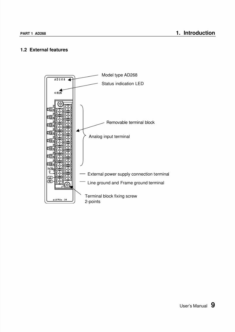
1.2 External features
Model type AD268
Status indication LED
Analog input terminal
External power supply connection terminal
Line ground and Frame ground terminal
Terminal block fixing screw
2-points
Removable terminal block

8/8/2019 T2 Analog I-O Modules
http://slidepdf.com/reader/full/t2-analog-i-o-modules 12/88
10 Analog I/O Modules (AD268 / DA264 / TC218)
2. Specifications PART 1 AD268
2. Specifications
This section describes the AD268 specifications.The general specification for the AD268 conforms to the specification for the T2 PLC.
2.1 Specifications
Item AD268
Input type Voltage input Current input
-5 to 5VBipolar
-10 to 10V
0 to 5V 0 to 20mA
0 to 10V
Input range
Unipolar
1 to 5V 4 to 20mA
Input impedance 1MΩ or more 250ΩNumber of input channels 8 channels
I/O allocation type X 8W (8 input registers XW are assigned)
Resolution 16-bit
Overall accuracy±0.2% FS (at 25°C)
±0.5% FS (0 to 55°C) (FS: ±10V)
Temperature drift ±100ppm/ °C or less
Conversion cycle Approx. 1ms/channel (Approx. 8ms/8 channels)
Insulation resistance 10MΩ or more
Withstand voltage1500Vac - 1 minute (between logic and analog circuits)500Vac - 1 minute (between analog circuit and external 24V)1500Vac - 1 minute (between analog circuit and FG/LG)
Status indication 1 green LED (On when normal)
Special function
Gain and offset calibration functionInput data averaging functionUnused channel skip functionExternal 24Vdc power voltage drop detection
External power supply 24Vdc ±10% - 120mA
Internal 5Vdc currentconsumption
300mA or less
External connection 20-pin removable terminal blockWeight Approx. 300g

8/8/2019 T2 Analog I-O Modules
http://slidepdf.com/reader/full/t2-analog-i-o-modules 13/88
User’s Manual 11
PART 1 AD268 2. Specifications
2.2 Internal block diagram
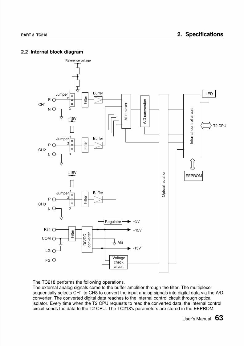
The AD268 performs the following operations.The external analog signals come to the buffer amplifier through the filter. The multiplexersequentially selects CH1 to CH8 to convert the input analog signals into digital data via the A/Dconverter. The converted digital data reaches to the internal control circuit through opticalisolator. Every time when the T2 CPU requests to read the converted data, the internal controlcircuit sends the data to the T2 CPU. The AD268's parameters are stored in the EEPROM.
F i l t e r
Buffer
M u l t i p l e x e r
1
3
2
Jumper
F i l t e r
Buffer1
3
2
Jumper
A / D c o n v e r s i o n
O p t i c a l i s o l a t i o n
CH1
P
N
I n t e r n a l c o n t r o l c i r c u i t
CH8
P
N
F i l t e r
D C / D C
c o n v e r t e r
Voltage
checkcircuit
Regulator +5V
+15V
-15V
AG
P24
COM
LG
FG
EEPROM
LED
T2 CPU

8/8/2019 T2 Analog I-O Modules
http://slidepdf.com/reader/full/t2-analog-i-o-modules 14/88
12 Analog I/O Modules (AD268 / DA264 / TC218)
3. Input Type Setting PART 1 AD268
3. Input Type Setting
The AD268 supports multiple input ranges, ±5V, ±10V, 0 to 5V, 0 to 10V, 1 to 5V, 0 to 20mA,or 4 to 20mA. The input range is selected by jumper plug setting and the parameter writing bythe T2 program.
The general flow for setting the input type is as follows.
(1) Set the jumper plugs to select voltage input or current input.(2) Mount the AD268 onto the T2 rack.(3) Turn on power to the T2 system.(4) Execute I/O allocation.(5) Program the "input type setting program". (see the next page)(6) Turn the T2 to RUN mode.
3.1 Jumper plug setting
8 jumper plugs are provided on the AD268 board.The jumper plug setting is for selecting either voltage input or current input.
JP1 is for channel 1, JP2 is for channel 2, ... JP8 is for channel 8.
Jumper plugs (JP1 to JP8)
1
3
Set the jumper plugs for each channel.
Side 1: Voltage inputSide 3: Current input
The factory setting is voltage input (side 1).
•Use a pair of tweezers to set the jumper plug.
•Pay attention not to touch the components onthe board other than the jumper plug.

8/8/2019 T2 Analog I-O Modules
http://slidepdf.com/reader/full/t2-analog-i-o-modules 15/88
User’s Manual 13
PART 1 AD268 3. Input Type Setting
3.2 Parameter setting by software
The input range of the AD268 is specified by writing the following parameter data into theAD268's buffer memory. To access the buffer memory, T2 user program (READ and WRITEinstructions) is required.When the parameter is set to the AD268, it is saved in the AD268's built-in EEPROM.Therefore, once the input type parameter is set, there is no need to execute the input typesetting operation.
T2 CPU AD268
Input type parameter data:
Input typeParameterdata Voltage input Current input
0 0 to 5V 0 to 20mA1 0 to 10V
2 1 to 5V 4 to 20mA4 ±5V5 ±10V
AD268 buffer memory address:
H8018 Input type for channel 1H8019 Input type for channel 2H801A Input type for channel 3H801B Input type for channel 4H801C Input type for channel 5H801D Input type for channel 6H801E Input type for channel 7H801F Input type for channel 8
The factory setting is ±10V range.
For details of the procedure to set the input type parameter, refer to section 6.
Buffer memory
User program
WRITE
READ
EEPROM

8/8/2019 T2 Analog I-O Modules
http://slidepdf.com/reader/full/t2-analog-i-o-modules 16/88
14 Analog I/O Modules (AD268 / DA264 / TC218)
4. Wiring PART 1 AD268
4. Wiring
4.1 Terminal arrangement
AD268 terminal block
1 1P1N 2
3 2P2N 4
5 3P3N 6
7 4P4N 8
9 5P5N 10
11 6P6N 12
13 7P7N 14
15 8P8N 16
17 P24COM 18
19 LGFG 20
TerminalNo.
Signalname
Function
1 1P2 1N
Channel 1 input
3 2P4 2N
Channel 2 input
5 3P6 3N
Channel 3 input
7 4P8 4N
Channel 4 input
9 5P
10 5N Channel 5 input11 6P12 6N
Channel 6 input
13 7P14 7N
Channel 7 input
15 8P16 8N
Channel 8 input
17 P24 External 24Vdc power (+)18 COM External 24Vdc power (-)19 LG Line filter ground20 FG Frame ground

8/8/2019 T2 Analog I-O Modules
http://slidepdf.com/reader/full/t2-analog-i-o-modules 17/88
User’s Manual 15
PART 1 AD268 4. Wiring
4.2 Signal wiring
Voltage input
Current input
External 24Vdc power supply
+15V
AG -15V
nP
nN
Internal circuit
Shielded twisted-pair cable
n : Channel number (1 to 8)AG : Analog groundFG : Frame ground
AG
250
+
-V
Set the jumperplug to Side 1
1
2
3
Voltage source
AD268
+15V
AG -15V
nP
nN
Internal circuit
Shielded twisted-pair cable
n : Channel number (1 to 8)AG : Analog groundFG : Frame ground
AG
250
+
-
↑↑↑↑
Set the jumperplug to Side 3
1
2
3
Current source
AD268
P24
COM
Internal circuit
Normally connect LG and FG,then connect to ground. (a)However, depending on thecondition, connect groundingindividually by opening LG and
FG. (b)
AD268
LG
FG
+
-24Vdc ±10%
(b) (a)
DC/DCconverter
+15V
-15VAG
8/8/2019 T2 Analog I-O Modules
http://slidepdf.com/reader/full/t2-analog-i-o-modules 18/88
16 Analog I/O Modules (AD268 / DA264 / TC218)
4. Wiring PART 1 AD268
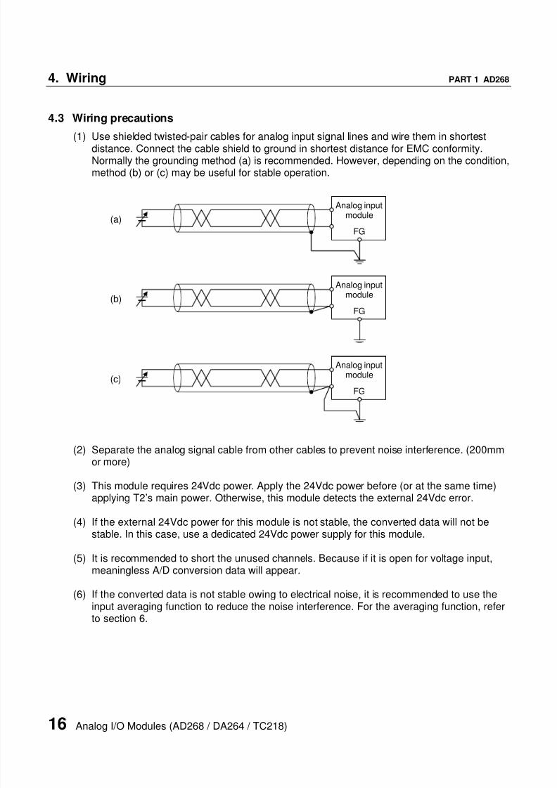
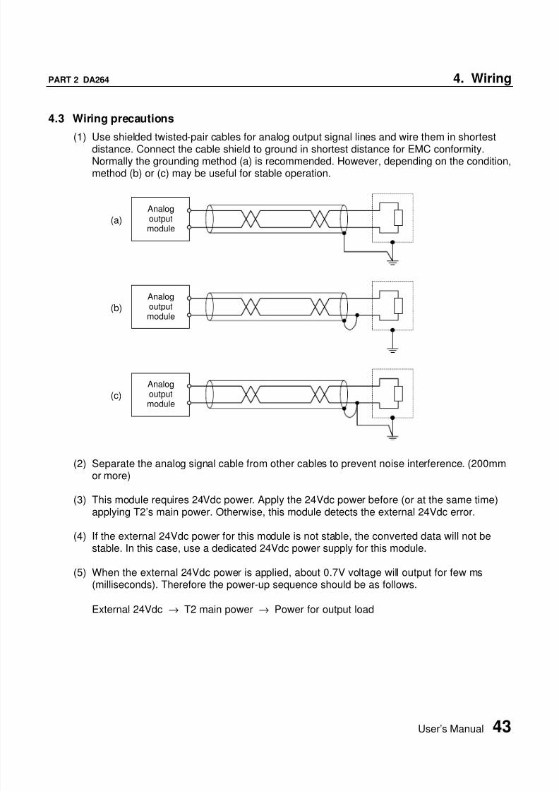
4.3 Wiring precautions
(1) Use shielded twisted-pair cables for analog input signal lines and wire them in shortestdistance. Connect the cable shield to ground in shortest distance for EMC conformity.Normally the grounding method (a) is recommended. However, depending on the condition,method (b) or (c) may be useful for stable operation.
(2) Separate the analog signal cable from other cables to prevent noise interference. (200mmor more)
(3) This module requires 24Vdc power. Apply the 24Vdc power before (or at the same time)applying T2’s main power. Otherwise, this module detects the external 24Vdc error.
(4) If the external 24Vdc power for this module is not stable, the converted data will not bestable. In this case, use a dedicated 24Vdc power supply for this module.
(5) It is recommended to short the unused channels. Because if it is open for voltage input,meaningless A/D conversion data will appear.
(6) If the converted data is not stable owing to electrical noise, it is recommended to use theinput averaging function to reduce the noise interference. For the averaging function, referto section 6.
Analog inputmodule
FG
(a)
Analog inputmodule
FG
(b)
Analog inputmodule
FG
(c)

8/8/2019 T2 Analog I-O Modules
http://slidepdf.com/reader/full/t2-analog-i-o-modules 19/88
User’s Manual 17
PART 1 AD268 5. I/O Allocation and Programming
5. I/O Allocation and Programming
5.1 Allocation to the T2 registersThe I/O type of the AD268 is "X 8W".When the automatic I/O allocation operation is performed with a AD268 mounted on the rack,the AD268 is allocated as "X 8W".The AD268 occupies the 8 consecutive input (XW) registers of the T2.In this manual, these assigned I/O registers are expressed as XW(n), XW(n+1), ... XW(n+7).
The following figure shows an example of I/O allocation window of the T-PDS programmingsoftware. In this case, the AD268 is mounted in the slot 0 of base unit BU218.
In the above example, the AD268 is allocated on the unit-0, slot-0. And 8 I/O registers, XW000to XW007 are assigned to the AD268.
P S 2 6 1
P U 2 3 4 E
N o s l o t
D I 3 2
V a c a n t
D O 3 2
A D 2 6 8
V a c a n t
V a c a n t
V a c a n t
V a c a n t

8/8/2019 T2 Analog I-O Modules
http://slidepdf.com/reader/full/t2-analog-i-o-modules 20/88
18 Analog I/O Modules (AD268 / DA264 / TC218)
5. I/O Allocation and Programming PART 1 AD268
5.2 A/D conversion data
The analog signals received by the AD268 are converted into the digital data in this module.These converted digital data are read by T2 CPU in the batch I/O processing and stored in theassigned input registers as follows.
XW(n) ........ A/D conversion data for channel 1XW(n+1) .... A/D conversion data for channel 2XW(n+2) .... A/D conversion data for channel 3XW(n+3) .... A/D conversion data for channel 4XW(n+4) .... A/D conversion data for channel 5XW(n+5) .... A/D conversion data for channel 6XW(n+6) .... A/D conversion data for channel 7XW(n+7) .... A/D conversion data for channel 8
The conversion data stored in the XW register is dependent on the input type as follows.
±±±±10V range:
A/D conversion dataInput voltage
Hexadecimal IntegerResolution
Upper limit +10.2 V H7F80 32640: : :
Full scale (positive) +10 V H7D00 32000: : :
+0.3125 mV H0001 1
0 0 V H0000 0-0.3125 mV HFFFF -1
: : :Full scale (negative) -10 V H8300 -32000
: : :Lower limit -10.2 V H8080 -32640
0.3125 mV / bit
+10.2V
HC000-16384
0
H3FFF
16383
+10V
H7D0032000
+5.1196V-5.12V-10.2V
-10V
H8300-32000
Digital value
Analog input
D = 3200 × A
D: Digital dataA: Analog signal (V)
8/8/2019 T2 Analog I-O Modules
http://slidepdf.com/reader/full/t2-analog-i-o-modules 21/88
User’s Manual 19
PART 1 AD268 5. I/O Allocation and Programming
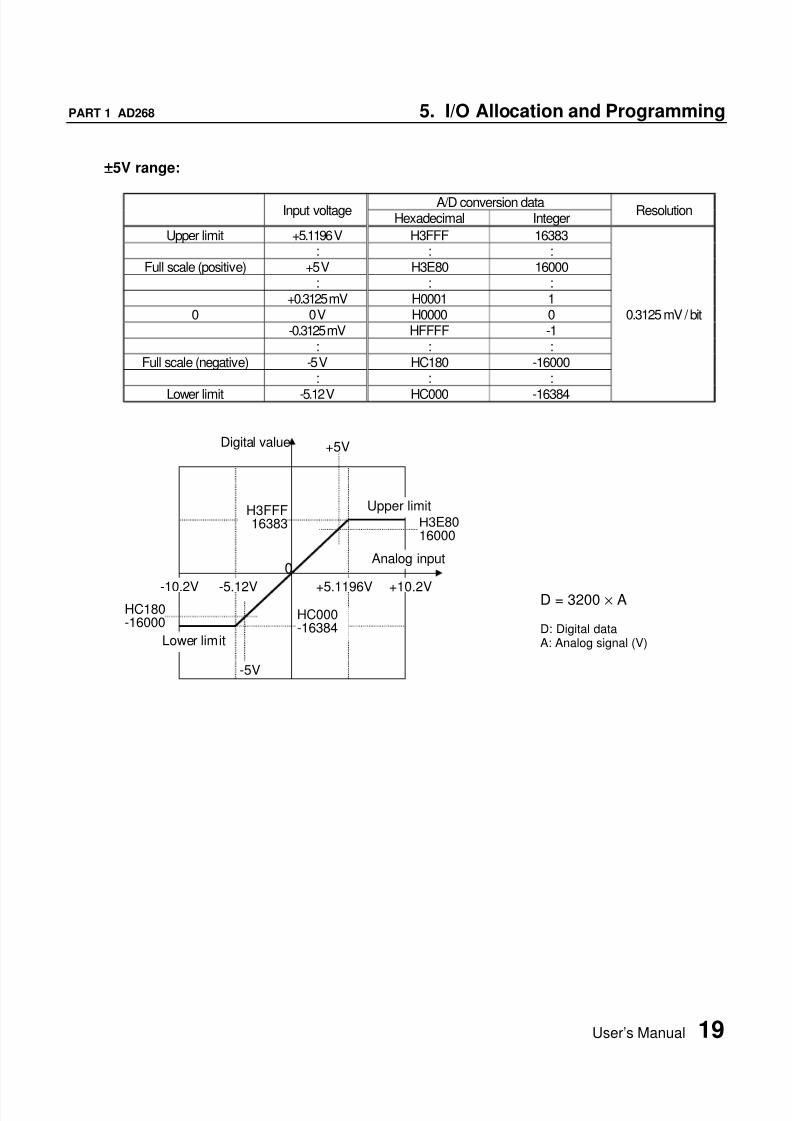
±±±±5V range:
A/D conversion dataInput voltage
Hexadecimal IntegerResolution
Upper limit +5.1196 V H3FFF 16383: : :
Full scale (positive) +5 V H3E80 16000: : :
+0.3125 mV H0001 10 0 V H0000 0
-0.3125 mV HFFFF -1: : :
Full scale (negative) -5 V HC180 -16000: : :
Lower limit -5.12 V HC000 -16384
0.3125 mV / bit
HC000-16384
0
H3FFF16383
+5V
H3E8016000
+5.1196V-5.12V
-5V
HC180-16000
Digital value
+10.2V-10.2V
Analog input
Upper limit
Lower limit
D = 3200 × A
D: Digital dataA: Analog signal (V)

8/8/2019 T2 Analog I-O Modules
http://slidepdf.com/reader/full/t2-analog-i-o-modules 22/88
20 Analog I/O Modules (AD268 / DA264 / TC218)
5. I/O Allocation and Programming PART 1 AD268
0 to 10V range:
A/D conversion dataInput voltage
Hexadecimal IntegerResolution
Upper limit +10.2 V H7F80 32640: : :
Full scale (positive) +10 V H7D00 32000: : :
+0.3125 mV H0001 10 0 V H0000 0
0.3125 mV / bit
D = 3200 × A
D: Digital dataA: Analog signal (V)
0
H3FFF16383
Analog input
+5.1196V
Digital value
+10.2V
H7D0032000
-10.2V
+10

8/8/2019 T2 Analog I-O Modules
http://slidepdf.com/reader/full/t2-analog-i-o-modules 23/88
User’s Manual 21
PART 1 AD268 5. I/O Allocation and Programming
0 to 5V / 0 to 20mA range:
Input voltage/current A/D conversion data0 to 5 V 0 to 20 mA Hexadecimal Integer
Resolution
Upper limit +5.1196 V +20.479 mA H3FFF 16383: : : :
Full scale (positive) +5 V +20 mA H3E80 16000: : : :
+0.3125 mV +0.00125 mA H0001 10 0 V 0 mA H0000 0
0.3125 mV / bit
1.25µA / bit
0 to 20mA range:
D = 800 × A
D: Digital dataA: Analog signal (mA)
0
H3FFF16383
Analog input
+5.1196V20.479mA
Digital value
+10.2V
H3E8016000
-10.2V
Upper limit
Lower limit
+5V20mA
0 to 5V range:
D = 3200 × A
D: Digital dataA: Analog signal (V)

8/8/2019 T2 Analog I-O Modules
http://slidepdf.com/reader/full/t2-analog-i-o-modules 24/88
22 Analog I/O Modules (AD268 / DA264 / TC218)
5. I/O Allocation and Programming PART 1 AD268
1 to 5V / 4 to 20mA range:
Input voltage/current A/D conversion data1 to 5 V 4 to 20 mA Hexadecimal Integer
Resolution
Upper limit +5.1196 V +20.479 mA H337F 13183: : : :
Full scale (positive) +5 V +20 mA H3200 12800: : : :
+1.0003125 V +4.00125 mA H0001 1Lower limit 1 V 4 mA H0000 0
0.3125 mV / bit
1.25µA / bit
4 to 20mA range:
D = 800 × A - 3200
D: Digital dataA: Analog signal (mA)
1 to 5V range:
D = 3200 × A - 3200
D: Digital dataA: Analog signal (V)
0Analog input value
+5.1196V20.479mA
Digital value
+10.2V-10.2V
Upper limit
Lower limit
+5V20mA
H320012800
H337F13183
1V4mA

8/8/2019 T2 Analog I-O Modules
http://slidepdf.com/reader/full/t2-analog-i-o-modules 25/88
User’s Manual 23
PART 1 AD268 5. I/O Allocation and Programming
5.3 Programming
To read the A/D conversion data, there is no need to use special instruction. The A/Dconversion data are automatically stored in the assigned input registers (XW registers).
For example, when the AD268 is allocated to XW000 to XW007, the A/D conversion data ofeach channel is stored as follows.
XW000 : Channel 1 A/D conversion dataXW001 : Channel 2 A/D conversion dataXW002 : Channel 3 A/D conversion dataXW003 : Channel 4 A/D conversion dataXW004 : Channel 5 A/D conversion dataXW005 : Channel 6 A/D conversion dataXW006 : Channel 7 A/D conversion dataXW007 : Channel 8 A/D conversion data
Therefore, in the user program, you can use these XW registers directly for the analog dataprocessing.
The program shown below is an example of simple comparison with the channel 1 analog data.
(±10V setting)
Line 1: When XW000 is greater than 25600 (channel 1 analog input is more than 8V), R0100is set to ON.
Line 2: When XW000 is in the range of -9600 to 9600 (channel 1 analog input is in the rangeof -3V to 3V), R0101 is set to ON.
Line 3: When XW000 is less than -16000 (channel 1 analog input is less than -5V), R0102 isset to ON.
8/8/2019 T2 Analog I-O Modules
http://slidepdf.com/reader/full/t2-analog-i-o-modules 26/88
24 Analog I/O Modules (AD268 / DA264 / TC218)
6. Parameters PART 1 AD268
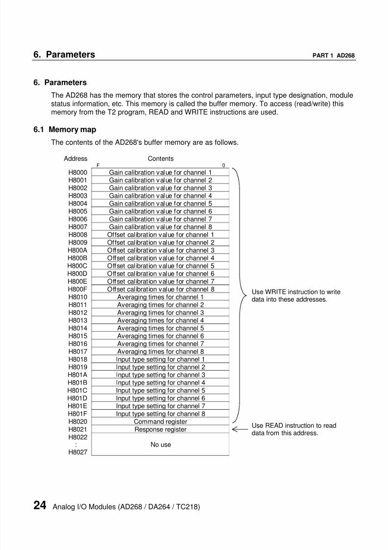
6. Parameters
The AD268 has the memory that stores the control parameters, input type designation, modulestatus information, etc. This memory is called the buffer memory. To access (read/write) thismemory from the T2 program, READ and WRITE instructions are used.
6.1 Memory map
The contents of the AD268's buffer memory are as follows.
Address ContentsF 0
H8000 Gain calibration value for channel 1H8001 Gain calibration value for channel 2H8002 Gain calibration value for channel 3H8003 Gain calibration value for channel 4H8004 Gain calibration value for channel 5H8005 Gain calibration value for channel 6H8006 Gain calibration value for channel 7H8007 Gain calibration value for channel 8H8008 Offset calibration value for channel 1H8009 Offset calibration value for channel 2H800A Offset calibration value for channel 3H800B Offset calibration value for channel 4H800C Offset calibration value for channel 5H800D Offset calibration value for channel 6H800E Offset calibration value for channel 7
H800F Offset calibration value for channel 8H8010 Averaging times for channel 1H8011 Averaging times for channel 2H8012 Averaging times for channel 3H8013 Averaging times for channel 4H8014 Averaging times for channel 5H8015 Averaging times for channel 6H8016 Averaging times for channel 7H8017 Averaging times for channel 8H8018 Input type setting for channel 1H8019 Input type setting for channel 2H801A Input type setting for channel 3
H801B Input type setting for channel 4H801C Input type setting for channel 5H801D Input type setting for channel 6H801E Input type setting for channel 7H801F Input type setting for channel 8H8020 Command registerH8021 Response registerH8022
:H8027
No use
Use WRITE instruction to writedata into these addresses.
Use READ instruction to readdata from this address.
8/8/2019 T2 Analog I-O Modules
http://slidepdf.com/reader/full/t2-analog-i-o-modules 27/88
User’s Manual 25
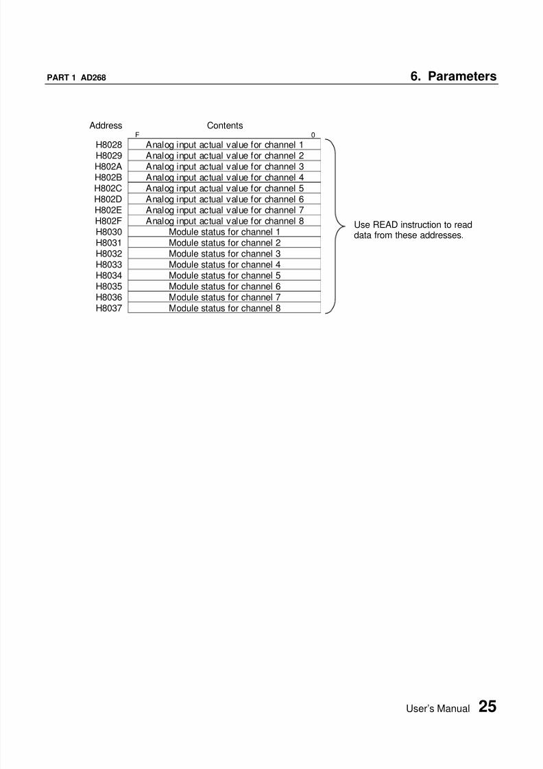
PART 1 AD268 6. Parameters
Address Contents
F 0H8028 Analog input actual value for channel 1H8029 Analog input actual value for channel 2H802A Analog input actual value for channel 3H802B Analog input actual value for channel 4H802C Analog input actual value for channel 5H802D Analog input actual value for channel 6H802E Analog input actual value for channel 7H802F Analog input actual value for channel 8H8030 Module status for channel 1H8031 Module status for channel 2H8032 Module status for channel 3
H8033 Module status for channel 4H8034 Module status for channel 5H8035 Module status for channel 6H8036 Module status for channel 7H8037 Module status for channel 8
Use READ instruction to readdata from these addresses.

8/8/2019 T2 Analog I-O Modules
http://slidepdf.com/reader/full/t2-analog-i-o-modules 28/88
26 Analog I/O Modules (AD268 / DA264 / TC218)
6. Parameters PART 1 AD268
Gain calibration value & Offset calibration value:(Gain: H8000 to H8007, Offset: H8008 to H800F)
At the factory shipment, the AD268 is calibrated for each input range. Therefore, there is noneed for user to calibrate normally.However, depending on the usage condition, field adjustments are required. For this purpose,the AD268 has the gain and offset calibration function.
In the AD268, the A/D conversion data is calculated as follows.
When the gain calibration value is G and the offset calibration value is O, the conversioncalculation is performed in the AD268 as follows.
X2 = (X1 + O) × G / FS
X1: Initial A/D conversion valueX2: Gain/offset processed valueO: Offset calibration value (buffer memory address H8008 to H800F)G: Gain calibration value (buffer memory address H8000 to H8007)FS: Full scale value
32000 for ±10V and 0 to 10V ranges16000 for ±5V, 0 to 5V and 0 to 20mA ranges12800 for 1 to 5V and 4 to 20mA ranges
The data setting range of the gain and offset calibration value are as follows.
Input type Gain calibration valueUpper limit 32000Default value 32000
±10V0 to 10V
Lower limit 10000Upper limit 16000Default value 16000
±5V0 to 5V
0 to 20mA Lower limit 5000Upper limit 12800Default value 12800
1 to 5V4 to 20mA
Lower limit 4000
Input type Offset calibration valueUpper limit 3200Default value 0All typesLower limit -3200
Analog input A/Dconversion
Offsetprocessing
Gainprocessing
A/D conversion data(read by T2 CPU)
8/8/2019 T2 Analog I-O Modules
http://slidepdf.com/reader/full/t2-analog-i-o-modules 29/88
User’s Manual 27
PART 1 AD268 6. Parameters
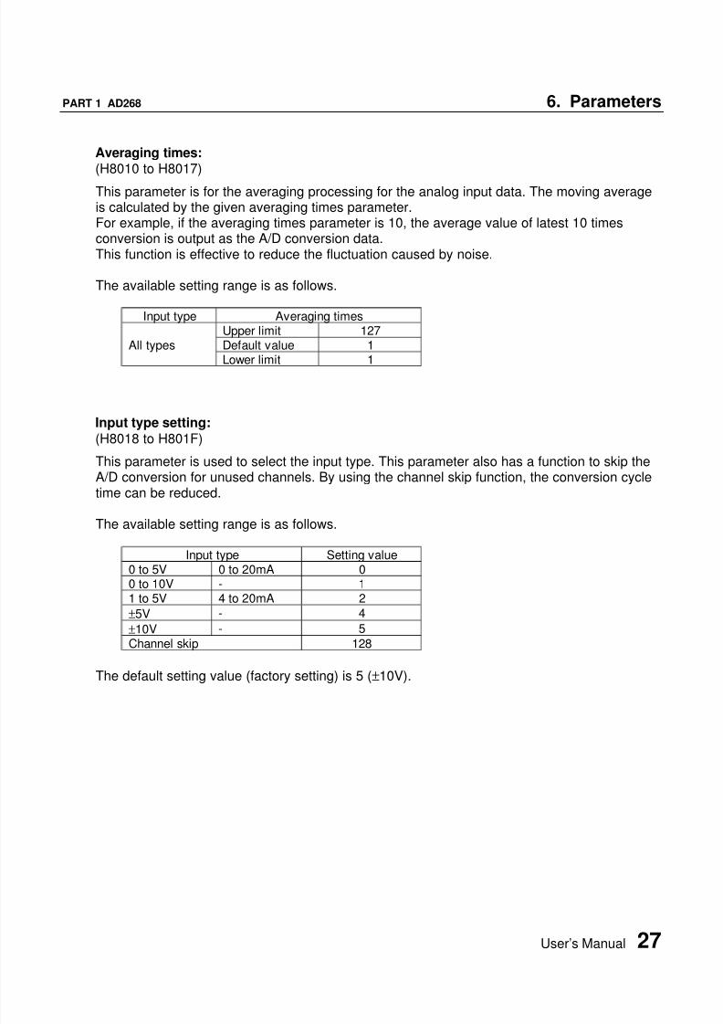
Averaging times:(H8010 to H8017)
This parameter is for the averaging processing for the analog input data. The moving averageis calculated by the given averaging times parameter.For example, if the averaging times parameter is 10, the average value of latest 10 timesconversion is output as the A/D conversion data.This function is effective to reduce the fluctuation caused by noise.
The available setting range is as follows.
Input type Averaging timesUpper limit 127Default value 1All types
Lower limit 1
Input type setting:
(H8018 to H801F)
This parameter is used to select the input type. This parameter also has a function to skip theA/D conversion for unused channels. By using the channel skip function, the conversion cycletime can be reduced.
The available setting range is as follows.
Input type Setting value0 to 5V 0 to 20mA 00 to 10V - 11 to 5V 4 to 20mA 2
±5V - 4
±10V - 5
Channel skip 128
The default setting value (factory setting) is 5 (±10V).

8/8/2019 T2 Analog I-O Modules
http://slidepdf.com/reader/full/t2-analog-i-o-modules 30/88
28 Analog I/O Modules (AD268 / DA264 / TC218)
6. Parameters PART 1 AD268
Command register:(H8020)
This register is used to issue the following commands to the AD268. To issue the command,write the command value by using WRITE instruction.
Value Command Description0 - Write 0 after the command processing is completed.
1 Parameter setWhen this command is issued, the parameters written intothe buffer memory are saved in the AD268 ’s EEPROM, andthe parameters become effective.
2 Reset commandUsed to reset the AD268 when some error has occurred.However if the error is caused by hardware or externalcondition, the reset command may not be effective.
The command register and the response register are used for hand-shaking. Refer to section6.2 for the parameter setting procedure.
Response register:(H8021)
This register shows the AD268’s response for the command issued. Check the status of thisregister using READ instruction.
Value Response Description0 - The requested command is not yet completed.
1 AcknowledgeWhen the issued command is completed, the responseregister comes 1.
The command register and the response register are used for hand-shaking. Refer to section6.2 for the parameter setting procedure.

8/8/2019 T2 Analog I-O Modules
http://slidepdf.com/reader/full/t2-analog-i-o-modules 31/88
User’s Manual 29
PART 1 AD268 6. Parameters
Analog input actual value:(H8028 to H802F)
These data show the original A/D conversion data before processing the gain and offsetcalibration.
Module status:(H8030 to H8037)
These data show the AD268’s operation status.
Bit position → F E D C B A 9 8 7 6 5 4 3 2 1 0
0 0 0 0
Bit Name Description0 to 2 Input type Shows the input type.
000 (0) = 0 to 5V/0 to 20mA001 (1) = 0 to 10V010 (2) = 1 to 5V/4 to 20mA
100 (4) = ±5V
101 (5) = ±10V3 to 5 - Reserved
6 Channel skip 1 when the channel skip is designated.7 Input type setting
error1 when the input type designation is invalid.
8 Wire break 1 when wire breakage is detected. (Effective only for 4 to 20mAinput)
9 Input limit 1 when the A/D conversion data is limited because of the rangeover.
A MPU error 1 when the AD268’s processor is not normal.B ROM status 1 when the AD268’s EEPROM is not normal.C DP-RAM status 1 when the AD268’s DP-RAM (buffer memory) is not normal.D - ReservedE External 24V error 1 when the external 24Vdc is not normal.F Initializing 1 during the AD268 is in initialization process.
8/8/2019 T2 Analog I-O Modules
http://slidepdf.com/reader/full/t2-analog-i-o-modules 32/88
30 Analog I/O Modules (AD268 / DA264 / TC218)
6. Parameters PART 1 AD268
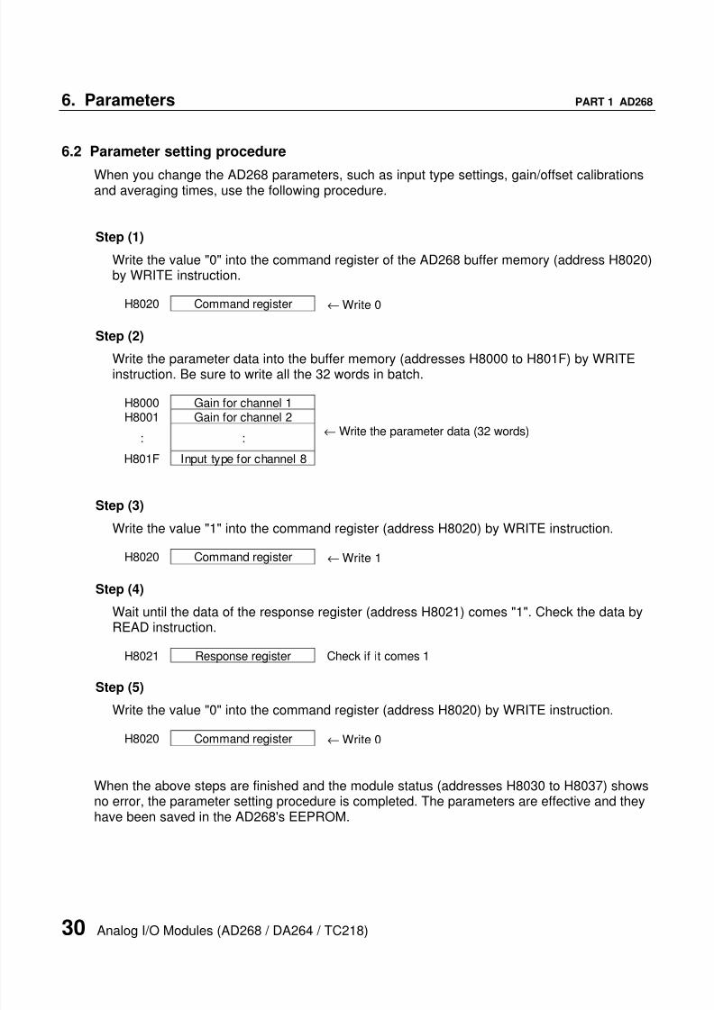
6.2 Parameter setting procedure
When you change the AD268 parameters, such as input type settings, gain/offset calibrationsand averaging times, use the following procedure.
Step (1)
Write the value "0" into the command register of the AD268 buffer memory (address H8020)by WRITE instruction.
H8020 Command register ← Write 0
Step (2)
Write the parameter data into the buffer memory (addresses H8000 to H801F) by WRITEinstruction. Be sure to write all the 32 words in batch.
H8000 Gain for channel 1H8001 Gain for channel 2
: :
H801F Input type for channel 8
← Write the parameter data (32 words)
Step (3)
Write the value "1" into the command register (address H8020) by WRITE instruction.
H8020 Command register ← Write 1
Step (4)
Wait until the data of the response register (address H8021) comes "1". Check the data byREAD instruction.
H8021 Response register Check if it comes 1
Step (5)
Write the value "0" into the command register (address H8020) by WRITE instruction.
H8020 Command register ← Write 0
When the above steps are finished and the module status (addresses H8030 to H8037) showsno error, the parameter setting procedure is completed. The parameters are effective and theyhave been saved in the AD268's EEPROM.

8/8/2019 T2 Analog I-O Modules
http://slidepdf.com/reader/full/t2-analog-i-o-modules 33/88
User’s Manual 31
PART 1 AD268 6. Parameters
6.3 Sample program for setting the parameters
A sample program to set the parameters is shown below.This is an example to set the input type as 0 to 10V range (type = 1) for each channel.In this sample program, it is assumed that he AD268 is allocated to XW000 to XW007.
For details of READ and WRITE instructions, refer to the T-series Instruction Set manual.
(Main program)
In this sample program, the rung 1 is activated at the beginning of RUN mode (at the secondscan) automatically. The input type is set to 0 to 10V for all 8 channels.When the parameter setting process is completed, the flags R1000 to R1002 are returned toOFF.
For reading the parameters from the AD268, there is no special procedure. Simply read the
data from the AD268’s buffer memory by using READ instruction.
Step (1):Writes 0 into thecommandregister (H8020).
Step (2):Writes parameters.
• Gain = 32000
• Offset = 0
• Average = 1
• Type = 1 (0-10V)Total 32 wordsstarting with
Step (3):Writes 1 into thecommandregister (H8020).
Step (4):Waits until theresponseregister (H8021)comes 1.
Step (5):Writes 0 into thecommand
register (H8020)to return to initialstate.
(H8020)
(H8000)
(H8020)
(H8021)
(H8020)
8/8/2019 T2 Analog I-O Modules
http://slidepdf.com/reader/full/t2-analog-i-o-modules 34/88
32 Analog I/O Modules (AD268 / DA264 / TC218)
7. Troubleshooting PART 1 AD268
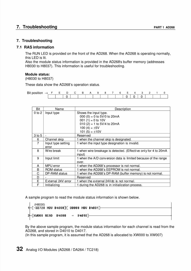
7. Troubleshooting
7.1 RAS informationThe RUN LED is provided on the front of the AD268. When the AD268 is operating normally,this LED is lit.Also the module status information is provided in the AD268‘s buffer memory (addressesH8030 to H8037). This information is useful for troubleshooting.
Module status:(H8030 to H8037)
These data show the AD268’s operation status.
Bit position → F E D C B A 9 8 7 6 5 4 3 2 1 0
0 0 0 0
Bit Name Description0 to 2 Input type Shows the input type.
000 (0) = 0 to 5V/0 to 20mA001 (1) = 0 to 10V010 (2) = 1 to 5V/4 to 20mA
100 (4) = ±5V101 (5) = ±10V
3 to 5 - Reserved6 Channel skip 1 when the channel skip is designated.
7 Input type settingerror
1 when the input type designation is invalid.
8 Wire break 1 when wire breakage is detected. (Effective only for 4 to 20mAinput)
9 Input limit 1 when the A/D conversion data is limited because of the rangeover.
A MPU error 1 when the AD268’s processor is not normal.B ROM status 1 when the AD268’s EEPROM is not normal.C DP-RAM status 1 when the AD268’s DP-RAM (buffer memory) is not normal.D - ReservedE External 24V error 1 when the external 24Vdc is not normal.F Initializing 1 during the AD268 is in initialization process.
A sample program to read the module status information is shown below.
By the above sample program, the module status information for each channel is read from theAD268, and stored in D4010 to D4017.(In this sample program, it is assumed that the AD268 is allocated to XW000 to XW007)
(H8030)

8/8/2019 T2 Analog I-O Modules
http://slidepdf.com/reader/full/t2-analog-i-o-modules 35/88
User’s Manual 33
PART 1 AD268 7. Troubleshooting
7.2 Troubleshooting
The table below shows the trouble and its remedy.
Trouble Modulestatus info
LED Module operation Cause Remedy
Input typesetting error
Bit 7 is ON ON(if the erroroccurs in allchannels, itis OFF)
The error channelstops theconversion. The A/Dconversion data is 0.
Invalid input typeparameter was set.
Set the correctinput typeparameter.
Analog signalwire breakage(4-20mA only)
Bit 8 is ON ON The A/D conversiondata of the channelis 0.
In the 4-20mAinput, less than4mA signal is input.
Check the analogsignal wire.
Analog signallimit over
Bit 9 is ON ON The A/D conversiondata of the channelis limited by the limitvalue.
Analog input signalis out of the range.
Check the signalsource (sensor).
MPU error Bit A is ON OFF The A/D conversionis stopped.
Internal processoroperation is notnormal.
Execute resetcommand, orcycle power offand on.
ROM error Bit B is ON OFF The A/D conversionis stopped.
EEPROM dataerror is detected.
Cycle power offand on.
DP-RAM error Bit C is ON OFF The A/D conversionis stopped.
Buffer memoryaccess error isoccurred.
Cycle power offand on.
External 24Verror Bit E is ON OFF The A/D conversionis stopped. Internal ±15Vvoltage is notnormal.
Check theexternal 24Vdcpower supply.

8/8/2019 T2 Analog I-O Modules
http://slidepdf.com/reader/full/t2-analog-i-o-modules 36/88
34 Analog I/O Modules (AD268 / DA264 / TC218)
8/8/2019 T2 Analog I-O Modules
http://slidepdf.com/reader/full/t2-analog-i-o-modules 37/88
User’s Manual 35
Part 2
4 Channel Analog Output Module
DA264
1. Introduction, 36 2. Specifications, 38 3. Output Type Setting, 40 4. Wiring, 415. I/O Allocation and Programming, 44 6. Parameters, 517. Troubleshooting, 56

8/8/2019 T2 Analog I-O Modules
http://slidepdf.com/reader/full/t2-analog-i-o-modules 38/88
36 Analog I/O Modules (AD268 / DA264 / TC218)
1. Introduction PART 2 DA264
1. Introduction
The DA264 is a 4 channel analog output module for the T2 series programmable controllers.The DA264 converts digital values given by the T2 program into the analog signals (voltage orcurrent).
1.1 DA264 Functions
The DA264 has the following functions.
1) 4 channels output per module2) Selectable output type
• ±5V
• ±10V
• 0 to 5V• 0 to 10V
• 1 to 5V
• 0 to 20mA
• 4 to 20mA3) 16-bit high-resolution D/A conversion4) High-speed (1ms/channel) conversion cycle5) Offset calibration function6) Output hold function

8/8/2019 T2 Analog I-O Modules
http://slidepdf.com/reader/full/t2-analog-i-o-modules 39/88
User’s Manual 37
PART 2 DA264 1. Introduction
1.2 External features
Model type DA264
Status indication LED
Analog output terminal
External power supply connection terminal
Line ground and Frame ground terminal
Terminal block fixing screw
2-points
Removable terminal block

8/8/2019 T2 Analog I-O Modules
http://slidepdf.com/reader/full/t2-analog-i-o-modules 40/88
38 Analog I/O Modules (AD268 / DA264 / TC218)
2. Specifications PART 2 DA264
2. Specifications
This section describes the DA264 specifications.The general specification for the DA264 conforms to the specification for the T2 PLC.
2.1 Specifications
Item DA264
Output type Voltage output Current output
-5 to 5VBipolar
-10 to 10V
0 to 5V 0 to 20mA
0 to 10V
Output range
Unipolar
1 to 5V 4 to 20mA
Load impedance 1kΩ or more 600Ω or less
Number of output channels 4 channels
I/O allocation type Y 4W (4 output registers YW are assigned)
Resolution 16-bit
Overall accuracy±0.2% FS (at 25°C)
±0.5% FS (0 to 55°C) (FS: ±10V)
Temperature drift ±100ppm/ °C or less
Conversion cycle Approx. 1ms/channel (Approx. 4ms/4 channels)
Insulation resistance 10MΩ or more
Withstand voltage1500Vac - 1 minute (between logic and analog circuits)500Vac - 1 minute (between analog circuit and external 24V)1500Vac - 1 minute (between analog circuit and FG/LG)
Status indication 1 green LED (On when normal)
Special functionOffset calibration functionOutput hold functionExternal 24Vdc power voltage drop detection
External power supply 24Vdc ±10% - 240mA
Internal 5Vdc currentconsumption
230mA or less
External connection 20-pin removable terminal block
Weight Approx. 300g

8/8/2019 T2 Analog I-O Modules
http://slidepdf.com/reader/full/t2-analog-i-o-modules 41/88
User’s Manual 39
PART 2 DA264 2. Specifications
2.2 Internal block diagram
The DA264 performs the following operations.The digital data for D/A conversion generated by the T2 program are written into the DA264.The written digital data are transferred to the D/A converter through optical isolator. Then theD/A converter converts the digital values to the analog signals.The generated analog signals are output to each channel (CH1 to CH4) via amplifier. Eachchannel has both the voltage output and the current output. However either voltage or currentoutput can be used.
I n t e r n a l c o n t r o l c i r c u i t
LED
T2 CPU
O p t i c a l i s o l a t i o n
D / A c o n v e r s i o n
Amplifier Buffer
CH1
P
N
Voltagecheckcircuit
+5V
+15V
-15VAG
P24
COM
LG
FG
D C / D C
c o n v e r t e r
F i l t e r
Regulator
Amplifier
P
N
TR
(V→V)
(V→I)
Amplifier Buffer
Amplifier
TR
(V→V)
(V→I)
Referencevoltage
Voltageout ut
Currentout ut
CH4
P
N
P
N
Voltageout ut
Currentout ut

8/8/2019 T2 Analog I-O Modules
http://slidepdf.com/reader/full/t2-analog-i-o-modules 42/88
40 Analog I/O Modules (AD268 / DA264 / TC218)
3. Output Type Setting PART 2 DA264
3. Output Type Setting
The DA264 supports multiple output ranges, ±5V, ±10V, 0 to 5V, 0 to 10V, 1 to 5V, 0 to 20mA,or 4 to 20mA. The output range is selected by writing the parameter into the DA264 by the T2program. The voltage or current output is selected by the DA264’s output terminals.
The general flow for setting the output type is as follows.
(1) Mount the DA264 onto the T2 rack.(2) Turn on power to the T2 system.(3) Execute I/O allocation.(4) Program the "output type setting program". (see below)(5) Turn the T2 to RUN mode.
3.1 Parameter setting by software
The output range of the DA264 is specified by writing the following parameter data into theDA264's buffer memory. To write the parameter into the buffer memory, T2 user program(WRITE instruction) is used.These parameter data are not maintained in the DA264. Therefore, program the output typesetting routine and execute it at each time of the beginning of the operation.
Output type parameter data:
Output typeParameterdata Voltage output Current output
0 0 to 5V 0 to 20mA
1 0 to 10V2 1 to 5V 4 to 20mA4 ±5V5 ±10V
DA264 buffer memory address:
H8004 Output type for channel 1H8005 Output type for channel 2H8006 Output type for channel 3H8007 Output type for channel 4
The factory setting is 0 to 5V / 0 to 20mA range.
Refer to section 6 for the sample program to set the output type.

8/8/2019 T2 Analog I-O Modules
http://slidepdf.com/reader/full/t2-analog-i-o-modules 43/88
User’s Manual 41
PART 2 DA264 4. Wiring
4. Wiring
4.1 Terminal arrangement
DA264 terminal block
1 1VP1VN 2
3 1CP1CN 4
5 2VP2VN 6
7 2CP2CN 8
9 3VP3VN 10
11 3CP3CN 12
13 4VP4VN 14
15 4CP4CN 16
17 P24COM 18
19 LGFG 20
TerminalNo.
Signalname
Function
1 1VP2 1VN
Channel 1 Voltage output
3 1CP4 1CN
Channel 1 Current output
5 2VP6 2VN
Channel 2 Voltage output
7 2CP8 2CN
Channel 2 Current output
9 3VP
10 3VN Channel 3 Voltage output11 3CP12 3CN
Channel 3 Current output
13 4VP14 4VN
Channel 4 Voltage output
15 4CP16 4CN
Channel 4 Current output
17 P24 External 24Vdc power (+)18 COM External 24Vdc power (-)19 LG Line filter ground20 FG Frame ground

8/8/2019 T2 Analog I-O Modules
http://slidepdf.com/reader/full/t2-analog-i-o-modules 44/88
42 Analog I/O Modules (AD268 / DA264 / TC218)
4. Wiring PART 2 DA264
4.2 Signal wiring
Voltage output
Current output
External 24Vdc power supply
AG
+15V
-15V
nVP
nVN
Internal circuit
Shielded twisted-pair cable
n : Channel number (1 to 4)AG : Analog ground
DA264
AG
+15V
-15V
nCP
nCN
Internal circuit
Shielded twisted-pair cable
n : Channel number (1 to 4)AG : Analog ground
DA264
+15V
DA264
P24
COM
LG
FG
DC/DCconverter
+
-24Vdc ±10%
Internal circuit
(b)(a) Normally connect LG and FG,then connect to ground. (a)However, depending on thecondition, connect groundingindividually by opening LG and
FG. (b)
+15V
-15VAG
8/8/2019 T2 Analog I-O Modules
http://slidepdf.com/reader/full/t2-analog-i-o-modules 45/88
User’s Manual 43
PART 2 DA264 4. Wiring
4.3 Wiring precautions
(1) Use shielded twisted-pair cables for analog output signal lines and wire them in shortestdistance. Connect the cable shield to ground in shortest distance for EMC conformity.Normally the grounding method (a) is recommended. However, depending on the condition,method (b) or (c) may be useful for stable operation.
(2) Separate the analog signal cable from other cables to prevent noise interference. (200mmor more)
(3) This module requires 24Vdc power. Apply the 24Vdc power before (or at the same time)applying T2’s main power. Otherwise, this module detects the external 24Vdc error.
(4) If the external 24Vdc power for this module is not stable, the converted data will not bestable. In this case, use a dedicated 24Vdc power supply for this module.
(5) When the external 24Vdc power is applied, about 0.7V voltage will output for few ms(milliseconds). Therefore the power-up sequence should be as follows.
External 24Vdc → T2 main power → Power for output load
(a)
Analogoutputmodule
(b)
Analogoutputmodule
(c)
Analogoutputmodule

8/8/2019 T2 Analog I-O Modules
http://slidepdf.com/reader/full/t2-analog-i-o-modules 46/88
44 Analog I/O Modules (AD268 / DA264 / TC218)
5. I/O Allocation and Programming PART 2 DA264
5. I/O Allocation and Programming
5.1 Allocation to the T2 registersThe I/O type of the DA264 is "Y 4W".When the automatic I/O allocation operation is performed with a DA264 mounted on the rack,the DA264 is allocated as "Y 4W".The DA264 occupies the 4 consecutive output (YW) registers of the T2.In this manual, these assigned I/O registers are expressed as YW(n), YW(n+1), YW(n+2) andYW(n+3).
The following figure shows an example of I/O allocation window of the T-PDS programmingsoftware. In this case, the DA264 is mounted in the slot 0 of base unit BU218.
In the above example, the DA264 is allocated on the unit-0, slot-0. And 4 I/O registers, YW000to YW003 are assigned to the DA264.
P S 2 6 1
P U 2 3 4 E
N o s l o t
D I 3 2
V a c a n t
D O 3 2
D A 2 6 4
V a c a n t
V a c a n t
V a c a n t
V a c a n t
8/8/2019 T2 Analog I-O Modules
http://slidepdf.com/reader/full/t2-analog-i-o-modules 47/88
User’s Manual 45
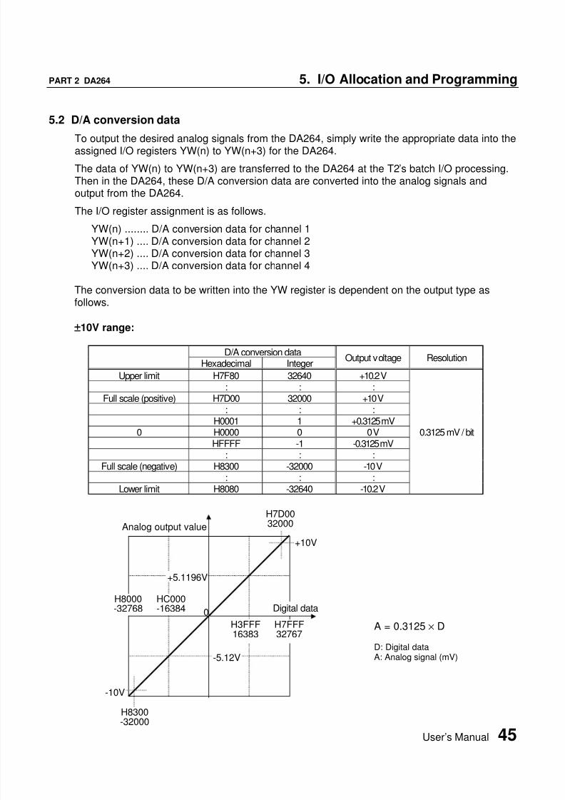
PART 2 DA264 5. I/O Allocation and Programming
5.2 D/A conversion data
To output the desired analog signals from the DA264, simply write the appropriate data into theassigned I/O registers YW(n) to YW(n+3) for the DA264.
The data of YW(n) to YW(n+3) are transferred to the DA264 at the T2’s batch I/O processing.Then in the DA264, these D/A conversion data are converted into the analog signals andoutput from the DA264.
The I/O register assignment is as follows.
YW(n) ........ D/A conversion data for channel 1YW(n+1) .... D/A conversion data for channel 2YW(n+2) .... D/A conversion data for channel 3YW(n+3) .... D/A conversion data for channel 4
The conversion data to be written into the YW register is dependent on the output type asfollows.
±±±±10V range:
D/A conversion dataHexadecimal Integer
Output voltage Resolution
Upper limit H7F80 32640 +10.2 V: : :
Full scale (positive) H7D00 32000 +10 V: : :
H0001 1 +0.3125 mV0 H0000 0 0 V
HFFFF -1 -0.3125 mV: : :
Full scale (negative) H8300 -32000 -10 V: : :
Lower limit H8080 -32640 -10.2 V
0.3125 mV / bit
A = 0.3125 × D
D: Digital dataA: Analog signal (mV)
HC000-16384
H8000-32768 0
H3FFF16383
H7FFF32767
Analog output value
+10V
H7D0032000
+5.1196V
-5.12V
-10V
H8300-32000
Digital data

8/8/2019 T2 Analog I-O Modules
http://slidepdf.com/reader/full/t2-analog-i-o-modules 48/88
46 Analog I/O Modules (AD268 / DA264 / TC218)
5. I/O Allocation and Programming PART 2 DA264
±±±±5V range:
D/A conversion dataHexadecimal Integer
Output voltage Resolution
Upper limit H3FFF 16383 +5.1196 V: : :
Full scale (positive) H3E80 16000 +5 V: : :
H0001 1 +0.3125 mV0 H0000 0 0 V
HFFFF -1 -0.3125 mV: : :
Full scale (negative) HC180 -16000 -5 V: : :
Lower limit HC000 -16384 -5.12 V
0.3125 mV / bit
A = 0.3125 × D
D: Digital dataA: Analog signal (mV)
-5V
Analog output value
0
H3FFF16383
+5.1196V
-5.12V
HC000-16384
+5V
H7FFF32767
HC180-16000
H8000-32768 Digital data
H3E8016000
Upper limit
Lower limit
8/8/2019 T2 Analog I-O Modules
http://slidepdf.com/reader/full/t2-analog-i-o-modules 49/88
User’s Manual 47
PART 2 DA264 5. I/O Allocation and Programming
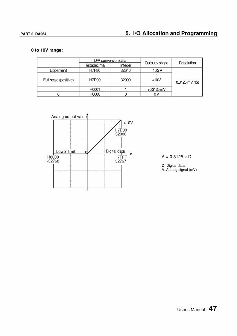
0 to 10V range:
D/A conversion dataHexadecimal Integer
Output voltage Resolution
Upper limit H7F80 32640 +10.2 V: : :
Full scale (positive) H7D00 32000 +10 V: : :
H0001 1 +0.3125 mV0 H0000 0 0 V
0.3125 mV / bit
A = 0.3125 × D
D: Digital dataA: Analog signal (mV)
H8000-32768
0
H7FFF32767
Analog output value+10V
H7D0032000
Digital dataLower limit

8/8/2019 T2 Analog I-O Modules
http://slidepdf.com/reader/full/t2-analog-i-o-modules 50/88
48 Analog I/O Modules (AD268 / DA264 / TC218)
5. I/O Allocation and Programming PART 2 DA264
0 to 5V / 0 to 20mA range:
D/A conversion data Output voltage/currentHexadecimal Integer 0 to 5 V 0 to 20 mA
Resolution
Upper limit H3FFF 16383 +5.1196 V +20.479 mA: : : :
Full scale (positive) H3E80 16000 +5 V +20 mA: : : :
H0001 1 +0.3125 mV +0.00125 mA0 H0000 0 0 V 0 mA
0.3125 mV / bit
1.25µA / bit
0 to 20mA range:
A = 1.25 × D
D: Digital dataA: Analog signal (µA)
0 to 5V range:
A = 0.3125 × D
D: Digital dataA: Analog signal (mV)
Analog output value
0
H3FFF16383
Upper limit+5V(+20mA)
H7FFF32767
H8000-32768
+5.1196V(+20.478mA)
H3E8016000
Digital dataLower limit
8/8/2019 T2 Analog I-O Modules
http://slidepdf.com/reader/full/t2-analog-i-o-modules 51/88
User’s Manual 49
PART 2 DA264 5. I/O Allocation and Programming
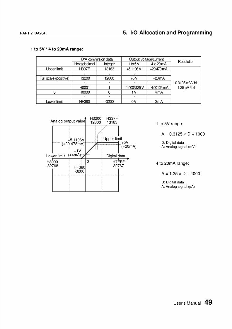
1 to 5V / 4 to 20mA range:
D/A conversion data Output voltage/currentHexadecimal Integer 1 to 5 V 4 to 20 mA
Resolution
Upper limit H337F 13183 +5.1196 V +20.479 mA: : : :
Full scale (positive) H3200 12800 +5 V +20 mA: : : :
H0001 1 +1.0003125 V +4.00125 mA0 H0000 0 1 V 4 mA
: : : :Lower limit HF380 -3200 0 V 0 mA
0.3125 mV / bit
1.25µA / bit
4 to 20mA range:
A = 1.25 × D + 4000
D: Digital data
A: Analog signal (µA)
1 to 5V range:
A = 0.3125 × D + 1000
D: Digital dataA: Analog signal (mV)
H8000-32768
0 H7FFF32767
Analog output valueH320012800
Digital data
+5V(+20mA)
+1V(+4mA)
HF380
-3200
H337F13183
+5.1196V(+20.478mA)
Lower limit
Upper limit

8/8/2019 T2 Analog I-O Modules
http://slidepdf.com/reader/full/t2-analog-i-o-modules 52/88
50 Analog I/O Modules (AD268 / DA264 / TC218)
5. I/O Allocation and Programming PART 2 DA264
5.3 Programming
To output the desired analog signal from the DA264, there is no need to use any specialinstruction. When the D/A conversion data is written in the assigned output register (YWregister), it is transferred to the DA264 and converted to the corresponding analog signal.
For example, when the DA264 is allocated to YW000 to YW003, the D/A conversion data ofeach channel is assigned as follows.
YW000 : Channel 1 D/A conversion dataYW001 : Channel 2 D/A conversion dataYW002 : Channel 3 D/A conversion dataYW003 : Channel 4 D/A conversion data
Therefore, in the user program, you can use any instructions to write data in these YW
registers for the analog data processing.
The program shown below is an example of simple increasing/decreasing of the channel 1
analog data. (±10V setting)
Rung 1: During R1000 is ON, YW000 data is increased by 32 (channel 1 analog output isincreased by 0.01V) every scan. It is upper-limited by 32000 (10V).
Rung 2: During R1001 is ON, YW000 data is decreased by 32 (channel 1 analog output isdecreased by 0.01V) every scan. It is lower-limited by -32000 (-10V).

8/8/2019 T2 Analog I-O Modules
http://slidepdf.com/reader/full/t2-analog-i-o-modules 53/88
User’s Manual 51
PART 2 DA264 6. Parameters
6. Parameters
The DA264 has the memory that stores the control parameters, output type designation,module status information, etc. This memory is called the buffer memory. To access(read/write) this memory from the T2 program, READ and WRITE instructions are used.
These parameter data are not maintained in the DA264. Therefore, you should write thenecessary parameter data at each time of the beginning of the operation.
6.1 Memory map
The contents of the DA264's buffer memory are as follows.
Address ContentsF 0
H8000 Offset calibration value for channel 1H8001 Offset calibration value for channel 2H8002 Offset calibration value for channel 3H8003 Offset calibration value for channel 4H8004 Output type setting for channel 1H8005 Output type setting for channel 2H8006 Output type setting for channel 3H8007 Output type setting for channel 4H8008 Analog output read-back value for channel 1H8009 Analog output read-back value for channel 2H800A Analog output read-back value for channel 3
H800B Analog output read-back value for channel 4H800C Module status for channel 1H800D Module status for channel 2H800E Module status for channel 3H800F Module status for channel 4
Use WRITE instruction to writedata into these addresses.
Use READ instruction to readdata from these addresses.

8/8/2019 T2 Analog I-O Modules
http://slidepdf.com/reader/full/t2-analog-i-o-modules 54/88
52 Analog I/O Modules (AD268 / DA264 / TC218)
6. Parameters PART 2 DA264
Offset calibration value:(H8000 to H8003)
At the factory shipment, the DA264 is calibrated for each output range. Therefore, there is noneed for user to calibrate normally.However, depending on the usage condition, field adjustments are required. For this purpose,the DA264 has the offset calibration function.
In the DA264, the D/A conversion is performed as follows.
When the offset calibration value is set, this value is added to the original D/A conversion data.Then D/A conversion is performed in the DA264.
The data setting range of the offset calibration value are as follows.
Output calibration rangeOffset calibration value
Voltage Current
Upper limit 127 +39.69 mV +158.75 µADefault value 0 0 0
Lower limit -127 -39.69 mV -158.75 µA
Analog outputOffsetprocessing
D/Aconversion
D/A conversion data(written by T2 CPU)
Amplifier
8/8/2019 T2 Analog I-O Modules
http://slidepdf.com/reader/full/t2-analog-i-o-modules 55/88
User’s Manual 53
PART 2 DA264 6. Parameters
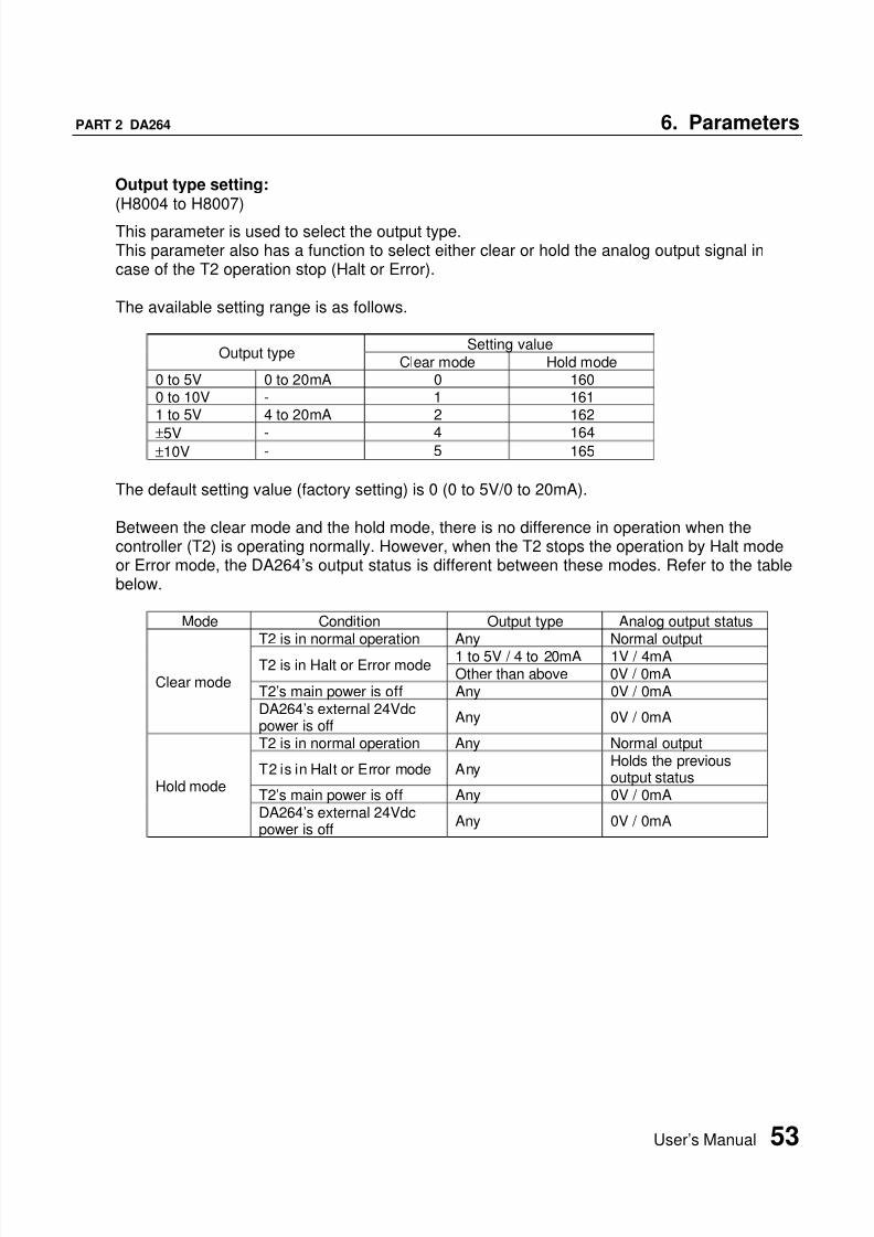
Output type setting:(H8004 to H8007)
This parameter is used to select the output type.This parameter also has a function to select either clear or hold the analog output signal incase of the T2 operation stop (Halt or Error).
The available setting range is as follows.
Setting valueOutput type
Clear mode Hold mode0 to 5V 0 to 20mA 0 1600 to 10V - 1 1611 to 5V 4 to 20mA 2 162
±5V - 4 164±10V - 5 165
The default setting value (factory setting) is 0 (0 to 5V/0 to 20mA).
Between the clear mode and the hold mode, there is no difference in operation when thecontroller (T2) is operating normally. However, when the T2 stops the operation by Halt modeor Error mode, the DA264’s output status is different between these modes. Refer to the tablebelow.
Mode Condition Output type Analog output statusT2 is in normal operation Any Normal output
1 to 5V / 4 to 20mA 1V / 4mAT2 is in Halt or Error mode
Other than above 0V / 0mAT2’s main power is off Any 0V / 0mA
Clear mode
DA264’s external 24Vdcpower is off
Any 0V / 0mA
T2 is in normal operation Any Normal output
T2 is in Halt or Error mode AnyHolds the previousoutput status
T2’s main power is off Any 0V / 0mAHold mode
DA264’s external 24Vdcpower is off
Any 0V / 0mA
8/8/2019 T2 Analog I-O Modules
http://slidepdf.com/reader/full/t2-analog-i-o-modules 56/88
54 Analog I/O Modules (AD268 / DA264 / TC218)
6. Parameters PART 2 DA264
Analog output read-back value:(H8008 to H800B)
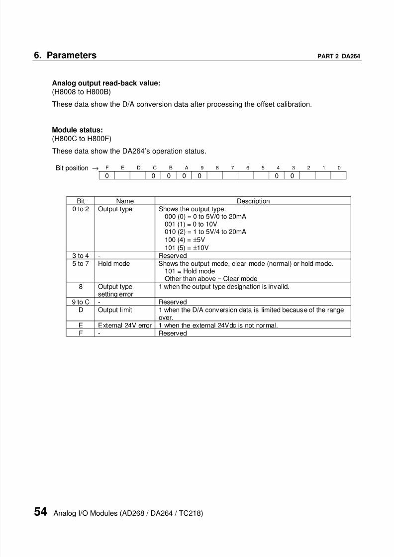
These data show the D/A conversion data after processing the offset calibration.
Module status:(H800C to H800F)
These data show the DA264’s operation status.
Bit position → F E D C B A 9 8 7 6 5 4 3 2 1 0
0 0 0 0 0 0 0
Bit Name Description0 to 2 Output type Shows the output type.
000 (0) = 0 to 5V/0 to 20mA001 (1) = 0 to 10V010 (2) = 1 to 5V/4 to 20mA
100 (4) = ±5V
101 (5) = ±10V3 to 4 - Reserved5 to 7 Hold mode Shows the output mode, clear mode (normal) or hold mode.
101 = Hold modeOther than above = Clear mode
8 Output type
setting error
1 when the output type designation is invalid.
9 to C - ReservedD Output limit 1 when the D/A conversion data is limited because of the range
over.E External 24V error 1 when the external 24Vdc is not normal.F - Reserved
8/8/2019 T2 Analog I-O Modules
http://slidepdf.com/reader/full/t2-analog-i-o-modules 57/88
User’s Manual 55
PART 2 DA264 6. Parameters
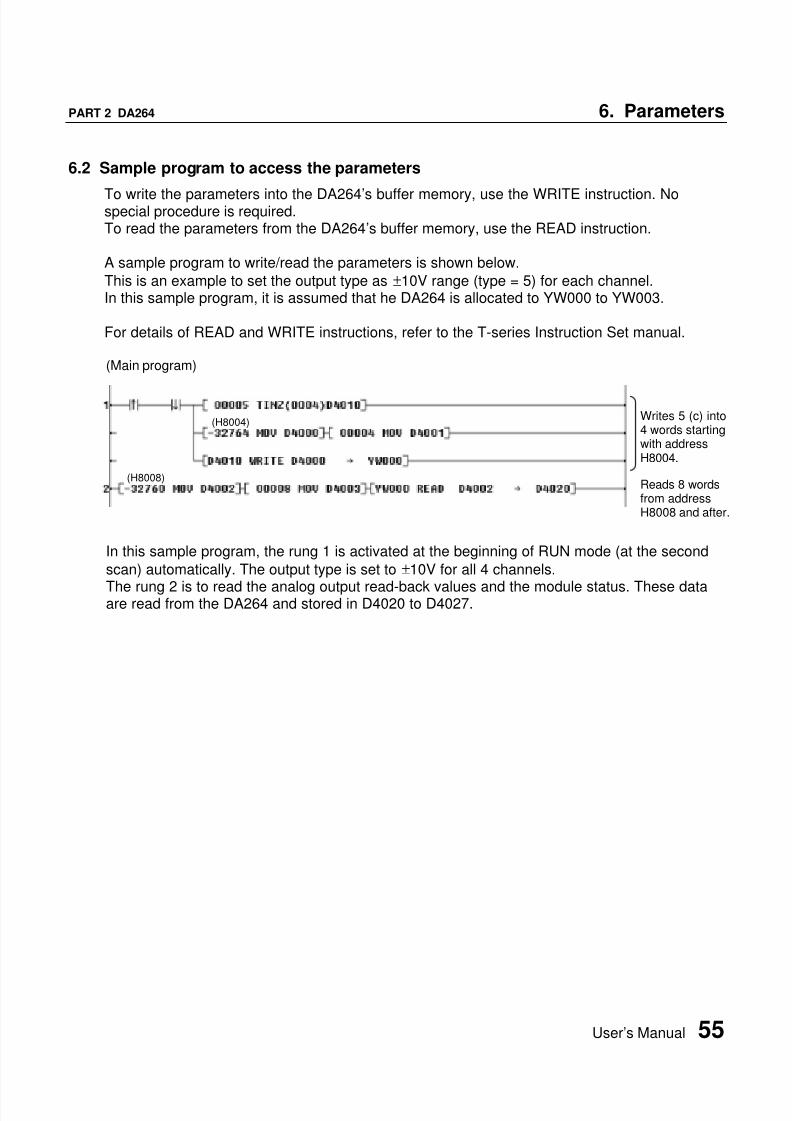
6.2 Sample program to access the parameters
To write the parameters into the DA264’s buffer memory, use the WRITE instruction. Nospecial procedure is required.To read the parameters from the DA264’s buffer memory, use the READ instruction.
A sample program to write/read the parameters is shown below.
This is an example to set the output type as ±10V range (type = 5) for each channel.In this sample program, it is assumed that he DA264 is allocated to YW000 to YW003.
For details of READ and WRITE instructions, refer to the T-series Instruction Set manual.
(Main program)
In this sample program, the rung 1 is activated at the beginning of RUN mode (at the second
scan) automatically. The output type is set to ±10V for all 4 channels.
The rung 2 is to read the analog output read-back values and the module status. These dataare read from the DA264 and stored in D4020 to D4027.
Writes 5 (c) into4 words startingwith addressH8004.
(H8004)
(H8008)Reads 8 wordsfrom addressH8008 and after.

8/8/2019 T2 Analog I-O Modules
http://slidepdf.com/reader/full/t2-analog-i-o-modules 58/88
56 Analog I/O Modules (AD268 / DA264 / TC218)
7. Troubleshooting PART 2 DA264
7. Troubleshooting
7.1 RAS informationThe RUN LED is provided on the front of the DA264. When the DA264 is operating normally,this LED is lit.Also the module status information is provided in the DA264‘s buffer memory (addressesH800C to H800F). This information is useful for troubleshooting.Refer to section 6 for the module status information and how to read it.
7.2 Troubleshooting
The table below shows the trouble and its remedy.
Trouble Modulestatus info
LED Module operation Cause Remedy
Output typesetting error
Bit 8 is ON ON(if the erroroccurs in allchannels, itis OFF)
The D/A conversioncontinues based onthe previous setting.
Invalid output typeparameter was set.
Set the correctoutput typeparameter.
D/Aconversiondata limit over
Bit D is ON ON The D/A conversiondata of the channelis limited by the limitvalue.
The written D/Aconversion data isout of the range.
Check the outputrage and writethe correct data.
External 24Verror
Bit E is ON OFF The D/A conversionis stopped. Output
signal is 0V/0mA.
Internal ±15Vvoltage is not
normal.
Check theexternal 24Vdc
power supply.

8/8/2019 T2 Analog I-O Modules
http://slidepdf.com/reader/full/t2-analog-i-o-modules 59/88
User’s Manual 57

8/8/2019 T2 Analog I-O Modules
http://slidepdf.com/reader/full/t2-analog-i-o-modules 60/88
58 Analog I/O Modules (AD268 / DA264 / TC218)
8/8/2019 T2 Analog I-O Modules
http://slidepdf.com/reader/full/t2-analog-i-o-modules 61/88
User’s Manual 59
Part 3
8 Channel Thermocouple Input Module
TC218
1. Introduction, 60 2. Specifications, 62 3. Input Type Setting, 64 4. Wiring, 66 5. I/O Allocation and Programming, 69 6. Parameters, 75 7. Troubleshooting, 83

8/8/2019 T2 Analog I-O Modules
http://slidepdf.com/reader/full/t2-analog-i-o-modules 62/88
60 Analog I/O Modules (AD268 / DA264 / TC218)
1. Introduction PART 3 TC218
1. Introduction
The TC218 is a thermocouple input module for the T2 series programmable controllers.The TC218 is used to measure the temperature using thermocouples. Thermocouples type K,J, or E can be used.
The TC218 can be used for ±100mV input also.When the TC218 is used for the thermocouple input, it has 7 channels of thermocouple input.The remaining 1 channel is used to measure the ambient temperature for cold junctioncompensation. For this purpose, a thermistor is attached with the TC218.
On the other hand, when the TC218 is used for ±100mV input, it has 8 channels of input.
1.1 TC218 Functions
The TC218 has the following functions.
1) 7 channels input per module for thermocouple input
8 channels input per module for ±100mV input2) Selectable input type
• Thermocouple type K (-200 to +1200 °C)
• Thermocouple type J (-200 to +800 °C)
• Thermocouple type E (-200 to +600 °C)
• ±100mV3) 16-bit high-resolution A/D conversion4) Built-in linearize function5) Cold junction compensation function6) Burnout detection function7) Input data averaging function
8) Gain and offset calibration function (±100mV input only)
8/8/2019 T2 Analog I-O Modules
http://slidepdf.com/reader/full/t2-analog-i-o-modules 63/88
User’s Manual 61
PART 3 TC218 1. Introduction
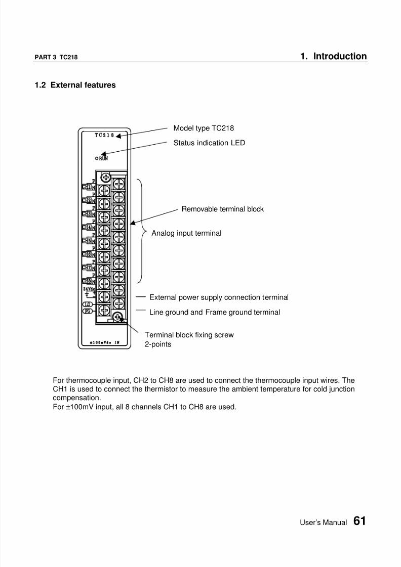
1.2 External features
For thermocouple input, CH2 to CH8 are used to connect the thermocouple input wires. TheCH1 is used to connect the thermistor to measure the ambient temperature for cold junction
compensation.For ±100mV input, all 8 channels CH1 to CH8 are used.
Model type TC218
Status indication LED
Analog input terminal
External power supply connection terminal
Line ground and Frame ground terminal
Terminal block fixing screw
2-points
Removable terminal block

8/8/2019 T2 Analog I-O Modules
http://slidepdf.com/reader/full/t2-analog-i-o-modules 64/88
62 Analog I/O Modules (AD268 / DA264 / TC218)
2. Specifications PART 3 TC218
2. Specifications
This section describes the TC218 specifications.The general specification for the TC218 conforms to the specification for the T2 PLC.
2.1 Specifications
Item TC218
Input type Voltage input Thermocouple input
mV input Type K Type J Type E
Input range -100 to +100mV
-200 to +1200
°C-200 to +800
°C-200 to +600
°CNumber of input channels 8 channels 7 channels 7 channels 7 channels
Input impedance 1MΩ or more
I/O allocation type X 8W (8 input registers XW are assigned)
Resolution 16-bit
Overall accuracy±0.2% FS (at 25°C)
±0.5% FS (0 to 55°C)
(FS: ±100mV (mV input) or 1400°C (type K))
Temperature drift ±100ppm/ °C or less
Conversion cycle Approx. 1ms/channel (Approx. 8ms/8 channels)
Insulation resistance 10MΩ or more
Withstand voltage
1500Vac - 1 minute (between logic and analog circuits)
500Vac - 1 minute (between analog circuit and external 24V)1500Vac - 1 minute (between analog circuit and FG/LG)
Status indication 1 green LED (On when normal)
Special function
Gain and offset calibration function (mV input only)Linearize function (thermocouple input)Cold junction compensation function (thermocouple input)Burnout detection function (thermocouple input)Input data averaging functionExternal 24Vdc power voltage drop detection
External power supply 24Vdc ±10% - 120mA
Internal 5Vdc current
consumption
300mA or less
External connection 20-pin removable terminal block
Weight Approx. 300g
8/8/2019 T2 Analog I-O Modules
http://slidepdf.com/reader/full/t2-analog-i-o-modules 65/88
User’s Manual 63
PART 3 TC218 2. Specifications
2.2 Internal block diagram
The TC218 performs the following operations.The external analog signals come to the buffer amplifier through the filter. The multiplexersequentially selects CH1 to CH8 to convert the input analog signals into digital data via the A/Dconverter. The converted digital data reaches to the internal control circuit through optical
isolator. Every time when the T2 CPU requests to read the converted data, the internal controlcircuit sends the data to the T2 CPU. The TC218's parameters are stored in the EEPROM.
F i l t e r
Buffer1
3
2Jumper
F i l t e r
Buffer1
3
2
Jumper
A / D
c o n v e r s i o n
O p t i c a l i s o l a t i o n
CH1
P
N
I n t e r n a l c o n t r o
l c i r c u i t
CH8
P
N
F i l t e r
D C
/ D C
c o n
v e r t e r
Voltagecheckcircuit
Regulator +5V
+15V
-15VAG
P24
COM
LG
FG
EEPROM
LED
T2 CPU
Reference voltage
+15V
F i l t e r
Buffer1
3
2
Jumper
CH2
P
N
+15V M u l t i p l e x e r

8/8/2019 T2 Analog I-O Modules
http://slidepdf.com/reader/full/t2-analog-i-o-modules 66/88
64 Analog I/O Modules (AD268 / DA264 / TC218)
3. Input Type Setting PART 3 TC218
3. Input Type Setting
The TC218 supports multiple input types, type K, type J, type E, or ±100mV. The input type isselected by jumper plug setting and the parameter writing by the T2 program.
Note that the input type can be selected either one, type K, type J, type E, or ±100mV, for allchannels. Any mixture settings among the channels are not allowed.
The general flow for setting the input type is as follows.
(1) Set the jumper plugs to select thermocouple input or mV input.(2) Mount the TC218 onto the T2 rack.(3) Turn on power to the T2 system.(4) Execute I/O allocation.
(5) Program the "input type setting program". (see the next page)(6) Turn the T2 to RUN mode.(7) Cycle power off/on
3.1 Jumper plug setting
8 jumper plugs are provided on the TC218 board.The jumper plug setting is for selecting either thermocouple input or mV input.
Jumper plugs (JP1 to JP8)
1
3
Set all the jumper plugs either side 1 or 3.
Side 1: Thermocouple input
Side 3: ±100mV input
The factory setting is ±100mV input (side 3).
•Use a pair of tweezers to set the jumper plug.
•Pay attention not to touch the components on theboard other than the jumper plug.

8/8/2019 T2 Analog I-O Modules
http://slidepdf.com/reader/full/t2-analog-i-o-modules 67/88
User’s Manual 65
PART 3 TC218 3. Input Type Setting
3.2 Parameter setting by software
The input type of the TC218 is specified by writing the following parameter data into theTC218's buffer memory. To access the buffer memory, T2 user program (READ and WRITEinstructions) is required.When the parameter is set to the TC218, it is saved in the TC218's built-in EEPROM.Therefore, once the input type parameter is set, there is no need to execute the input typesetting operation.
T2 CPU TC218
Input type parameter data:
Parameterdata
Input type
0 Type K thermocouple1 Type J thermocouple
2 Type E thermocouple5 ±100mV
TC218 buffer memory address:
H8018 Input type for channel 1H8019 Input type for channel 2H801A Input type for channel 3H801B Input type for channel 4H801C Input type for channel 5H801D Input type for channel 6H801E Input type for channel 7H801F Input type for channel 8
Set the same parameter data for all 8 channels.The factory setting is ±100mV range.
For details of the procedure to set the input type parameter, refer to section 6.
Buffer memory
User program
WRITE
READ
EEPROM

8/8/2019 T2 Analog I-O Modules
http://slidepdf.com/reader/full/t2-analog-i-o-modules 68/88
66 Analog I/O Modules (AD268 / DA264 / TC218)
4. Wiring PART 3 TC218
4. Wiring
4.1 Terminal arrangement
TC218 terminal block
1 1P1N 2
3 2P2N 4
5 3P3N 6
7 4P4N 8
9 5P5N 10
11 6P6N 12
13 7P7N 14
15 8P8N 16
17 P24COM 18
19 LGFG 20
TerminalNo.
Signalname
Function
1 1P2 1N
Channel 1 input
3 2P4 2N
Channel 2 input
5 3P6 3N
Channel 3 input
7 4P8 4N
Channel 4 input
9 5P
10 5N Channel 5 input11 6P12 6N
Channel 6 input
13 7P14 7N
Channel 7 input
15 8P16 8N
Channel 8 input
17 P24 External 24Vdc power (+)18 COM External 24Vdc power (-)19 LG Line filter ground20 FG Frame ground

8/8/2019 T2 Analog I-O Modules
http://slidepdf.com/reader/full/t2-analog-i-o-modules 69/88
User’s Manual 67
PART 3 TC218 4. Wiring
4.2 Signal wiring
±±±±100mV input (CH1 to CH8)
Thermocouple input
CH1
CH2 to CH8
Set the jumperplug to Side 3
+15V
AG -15V
nP
nN
Internal circuit
Shielded twisted-pair cable
n : Channel number (1 to 8)AG : Analog groundFG : Frame ground
+
-V
1
2
3
Voltage source
TC218
+15V
+15V
AG -15V
1P
1N
1
23
TC218
Set the jumperplug to Side 1
+15V
AG -15V
nP
nN
Internal circuitn : Channel number (2 to 8)
AG : Analog groundFG : Frame ground
1
2
3
Set the jumper
plug to Side 1
+15V
Thermocouple cablePositive side
Negative side
Connect the thermistorattached to the TC218

8/8/2019 T2 Analog I-O Modules
http://slidepdf.com/reader/full/t2-analog-i-o-modules 70/88
68 Analog I/O Modules (AD268 / DA264 / TC218)
4. Wiring PART 3 TC218
External 24Vdc power supply
4.3 Wiring precautions
(1) The thermocouple signal is weak voltage. Pay attention to prevent noise interference.
• Shortest cable distance
• Cable shield and grounding
• Separation from other cables
(2) This module requires 24Vdc power. Apply the 24Vdc power before (or at the same time)applying T2’s main power. Otherwise, this module detects the external 24Vdc error.
(3) If the external 24Vdc power for this module is not stable, the converted data will not bestable. In this case, use a dedicated 24Vdc power supply for this module.
(4) It is recommended to short the unused channels. Because if it is open, meaningless A/Dconversion data will appear.
(5) If the converted data is not stable owing to electrical noise, it is recommended to use the
input averaging function to reduce the noise interference. For the averaging function, referto section 6.
(6) When this module is used for thermocouple input, connect the thermistor to channel 1(CH1). The thermistor is attached with this module.
P24
COM
Internal circuit
Normally connect LG and FG,then connect to ground. (a)
However, depending on thecondition, connect groundingindividually by opening LG andFG. (b)
TC218
LG
FG
+
-24Vdc ±10%
(b) (a)
DC/DCconverter
+15V
-15VAG

8/8/2019 T2 Analog I-O Modules
http://slidepdf.com/reader/full/t2-analog-i-o-modules 71/88
User’s Manual 69
PART 3 TC218 5. I/O Allocation and Programming
5. I/O Allocation and Programming
5.1 Allocation to the T2 registersThe I/O type of the TC218 is "X 8W".When the automatic I/O allocation operation is performed with a TC218 mounted on the rack,the TC218 is allocated as "X 8W".The TC218 occupies the 8 consecutive input (XW) registers of the T2.In this manual, these assigned I/O registers are expressed as XW(n), XW(n+1), ... XW(n+7).
The following figure shows an example of I/O allocation window of the T-PDS programmingsoftware. In this case, the TC218 is mounted in the slot 0 of base unit BU218.
In the above example, the TC218 is allocated on the unit-0, slot-0. And 8 I/O registers, XW000to XW007 are assigned to the TC218.
P S 2 6 1
P U 2 3 4 E
N o s l o t
D I 3 2
V a c a n t
D O 3 2
T C 2 1 8
V a c a n t
V a c a n t
V a c a n t
V a c a n t
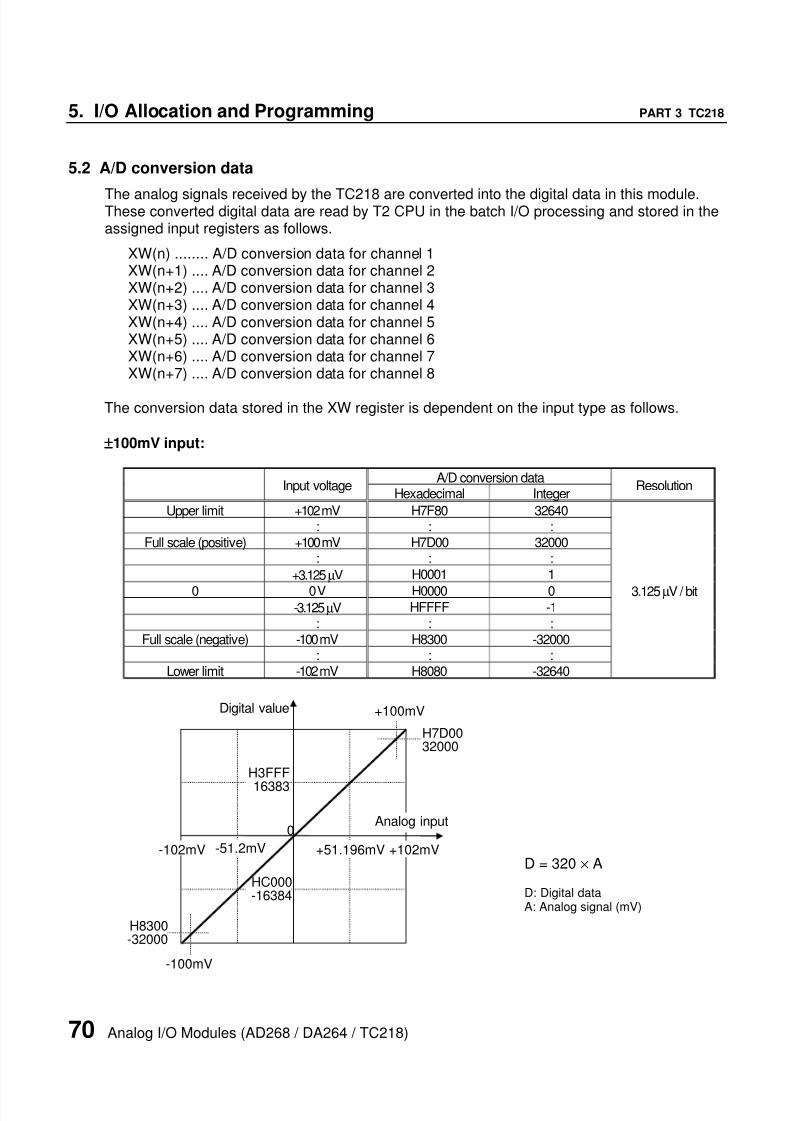
8/8/2019 T2 Analog I-O Modules
http://slidepdf.com/reader/full/t2-analog-i-o-modules 72/88
70 Analog I/O Modules (AD268 / DA264 / TC218)
5. I/O Allocation and Programming PART 3 TC218
5.2 A/D conversion data
The analog signals received by the TC218 are converted into the digital data in this module.These converted digital data are read by T2 CPU in the batch I/O processing and stored in theassigned input registers as follows.
XW(n) ........ A/D conversion data for channel 1XW(n+1) .... A/D conversion data for channel 2XW(n+2) .... A/D conversion data for channel 3XW(n+3) .... A/D conversion data for channel 4XW(n+4) .... A/D conversion data for channel 5XW(n+5) .... A/D conversion data for channel 6XW(n+6) .... A/D conversion data for channel 7XW(n+7) .... A/D conversion data for channel 8
The conversion data stored in the XW register is dependent on the input type as follows.
±±±±100mV input:
A/D conversion dataInput voltage
Hexadecimal IntegerResolution
Upper limit +102 mV H7F80 32640: : :
Full scale (positive) +100 mV H7D00 32000: : :
+3.125µV H0001 1
0 0 V H0000 0-3.125µV HFFFF -1
: : :Full scale (negative) -100 mV H8300 -32000
: : :Lower limit -102 mV H8080 -32640
3.125µV / bit
+102mV
HC000-16384
0
H3FFF
16383
+100mV
H7D0032000
+51.196mV-51.2mV-102mV
-100mV
H8300-32000
Digital value
Analog input
D = 320 × A
D: Digital dataA: Analog signal (mV)

8/8/2019 T2 Analog I-O Modules
http://slidepdf.com/reader/full/t2-analog-i-o-modules 73/88
User’s Manual 71
PART 3 TC218 5. I/O Allocation and Programming
Thermocouple (type K) input:
A/D conversion dataInputtemperature Hexadecimal Integer
Resolution
Burnout detection - H7FFF 32767
Upper limit +1370°C H6B08 27400
: : :
Full scale (positive) +1200°C H5DC0 24000
: : :
+0.05°C H0001 1
0 0 V H0000 0
-0.05°C HFFFF -1
: : :
Full scale (negative) -200°C HF060 -4000
: : :
Lower limit -270°C HEAE8 -5400
0.05 °C / bit
D = 20 × A
D: Digital data
A: Temperature (°C)
0Temperature
HF060-4000
Digital vale
-200°C
Upper limit
+1200°C
H5DC024000
Lower limit

8/8/2019 T2 Analog I-O Modules
http://slidepdf.com/reader/full/t2-analog-i-o-modules 74/88
72 Analog I/O Modules (AD268 / DA264 / TC218)
5. I/O Allocation and Programming PART 3 TC218
Thermocouple (type J) input:
A/D conversion dataInputtemperature Hexadecimal Integer
Resolution
Burnout detection - H7FFF 32767
Upper limit +1200°C H5DC0 24000
: : :
Full scale (positive) +800°C H3E80 16000
: : :
+0.05°C H0001 1
0 0 V H0000 0
-0.05°C HFFFF -1
: : :
Full scale (negative) -200°C HF060 -4000
: : :
Lower limit -210°C HEF98 -4200
0.05 °C / bit
D = 20 × A
D: Digital data
A: Temperature (°C)
0 TemperatureHF060-4000
Digital vale
-200°C
Upper limit
+800°C
H3E8016000
Lower limit

8/8/2019 T2 Analog I-O Modules
http://slidepdf.com/reader/full/t2-analog-i-o-modules 75/88
User’s Manual 73
PART 3 TC218 5. I/O Allocation and Programming
Thermocouple (type E) input:
A/D conversion dataInputtemperature Hexadecimal Integer
Resolution
Burnout detection - H7FFF 32767
Upper limit +1000°C H4E20 20000
: : :
Full scale (positive) +600°C H2EE0 12000
: : :
+0.05°C H0001 1
0 0 V H0000 0
-0.05°C HFFFF -1
: : :
Full scale (negative) -200°C HF060 -4000
: : :
Lower limit -270°C HEAE8 -5400
0.05 °C / bit
D = 20 × A
D: Digital data
A: Temperature (°C)
0 TemperatureHF060-4000
Digital vale
-200°C
Upper limit
+600°C
H2EE012000
Lower limit

8/8/2019 T2 Analog I-O Modules
http://slidepdf.com/reader/full/t2-analog-i-o-modules 76/88
74 Analog I/O Modules (AD268 / DA264 / TC218)
5. I/O Allocation and Programming PART 3 TC218
5.3 Programming
To read the A/D conversion data, there is no need to use special instruction. The A/Dconversion data are automatically stored in the assigned input registers (XW registers).
For example, when the TC218 is allocated to XW000 to XW007, the A/D conversion data ofeach channel is stored as follows.
XW000 : Channel 1 A/D conversion dataXW001 : Channel 2 A/D conversion dataXW002 : Channel 3 A/D conversion dataXW003 : Channel 4 A/D conversion dataXW004 : Channel 5 A/D conversion dataXW005 : Channel 6 A/D conversion dataXW006 : Channel 7 A/D conversion dataXW007 : Channel 8 A/D conversion data
Therefore, in the user program, you can use these XW registers directly for the analog dataprocessing.
The program shown below is an example of simple comparison with the channel 2 input data.(Thermocouple type K setting)
By the above program, the ON/OFF status of the internal relays R0200 to R0203 are changedas follows.
Status of the internal relaysTemperature XW001 data
R0200 R0201 R0202 R0203
More than 550 °C 11000 < XW001 ON ON OFF OFF
510 to 550 °C 10200 < XW001 ≤ 11000 OFF ON OFF OFF490 to 510 °C 9800 ≤ XW001 ≤ 10200 OFF OFF OFF OFF
450 to 490 °C 9000 ≤ XW001 < 9800 OFF OFF ON OFF
Less than 450 °C XW001 < 9000 OFF OFF ON ON
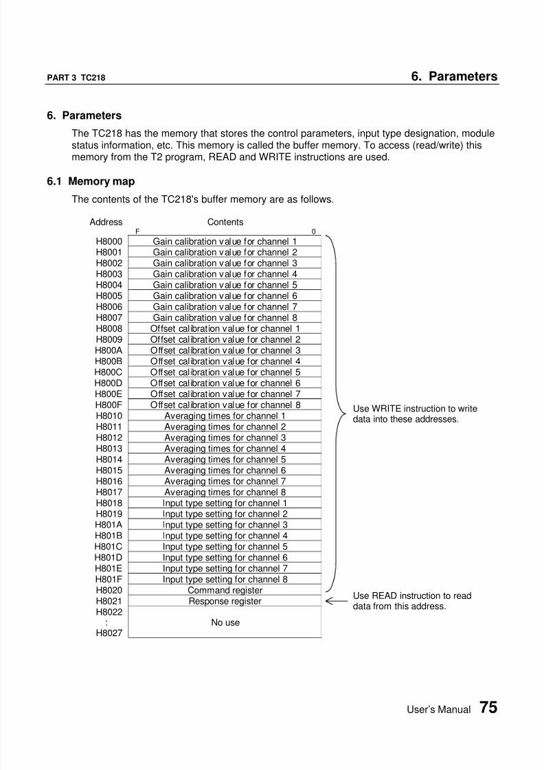
8/8/2019 T2 Analog I-O Modules
http://slidepdf.com/reader/full/t2-analog-i-o-modules 77/88
User’s Manual 75
PART 3 TC218 6. Parameters
6. Parameters
The TC218 has the memory that stores the control parameters, input type designation, modulestatus information, etc. This memory is called the buffer memory. To access (read/write) thismemory from the T2 program, READ and WRITE instructions are used.
6.1 Memory map
The contents of the TC218's buffer memory are as follows.
Address ContentsF 0
H8000 Gain calibration value for channel 1H8001 Gain calibration value for channel 2H8002 Gain calibration value for channel 3H8003 Gain calibration value for channel 4H8004 Gain calibration value for channel 5H8005 Gain calibration value for channel 6H8006 Gain calibration value for channel 7H8007 Gain calibration value for channel 8H8008 Offset calibration value for channel 1H8009 Offset calibration value for channel 2H800A Offset calibration value for channel 3H800B Offset calibration value for channel 4H800C Offset calibration value for channel 5H800D Offset calibration value for channel 6H800E Offset calibration value for channel 7
H800F Offset calibration value for channel 8H8010 Averaging times for channel 1H8011 Averaging times for channel 2H8012 Averaging times for channel 3H8013 Averaging times for channel 4H8014 Averaging times for channel 5H8015 Averaging times for channel 6H8016 Averaging times for channel 7H8017 Averaging times for channel 8H8018 Input type setting for channel 1H8019 Input type setting for channel 2H801A Input type setting for channel 3
H801B Input type setting for channel 4H801C Input type setting for channel 5H801D Input type setting for channel 6H801E Input type setting for channel 7H801F Input type setting for channel 8H8020 Command registerH8021 Response registerH8022
:H8027
No use
Use WRITE instruction to writedata into these addresses.
Use READ instruction to readdata from this address.
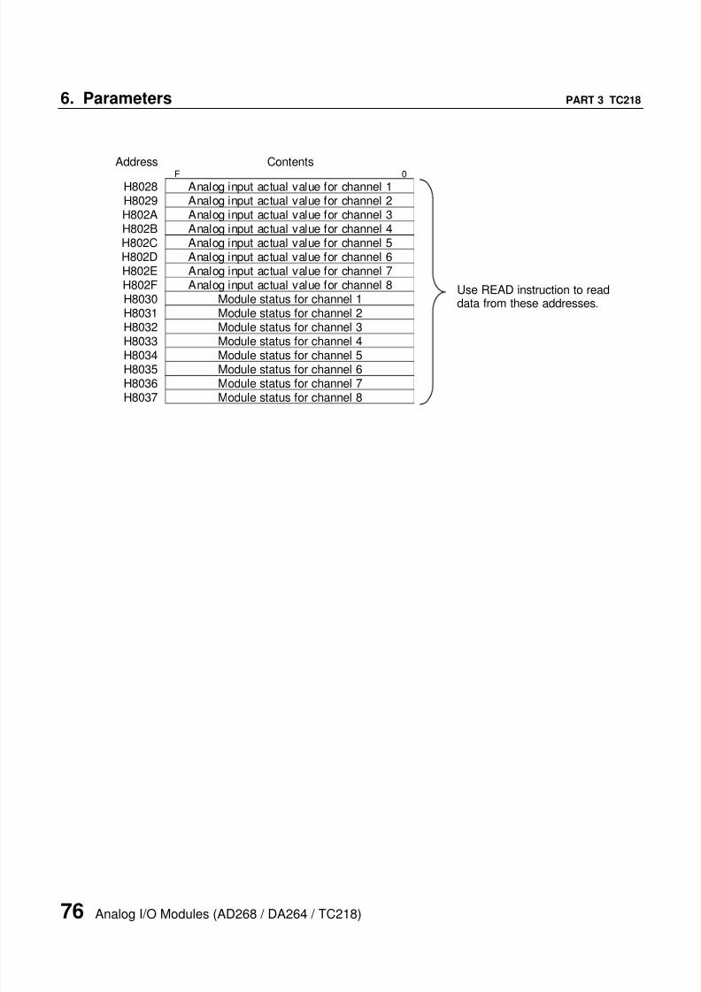
8/8/2019 T2 Analog I-O Modules
http://slidepdf.com/reader/full/t2-analog-i-o-modules 78/88
76 Analog I/O Modules (AD268 / DA264 / TC218)
6. Parameters PART 3 TC218
Address Contents
F 0H8028 Analog input actual value for channel 1H8029 Analog input actual value for channel 2H802A Analog input actual value for channel 3H802B Analog input actual value for channel 4H802C Analog input actual value for channel 5H802D Analog input actual value for channel 6H802E Analog input actual value for channel 7H802F Analog input actual value for channel 8H8030 Module status for channel 1H8031 Module status for channel 2H8032 Module status for channel 3
H8033 Module status for channel 4H8034 Module status for channel 5H8035 Module status for channel 6H8036 Module status for channel 7H8037 Module status for channel 8
Use READ instruction to readdata from these addresses.

8/8/2019 T2 Analog I-O Modules
http://slidepdf.com/reader/full/t2-analog-i-o-modules 79/88
User’s Manual 77
PART 3 TC218 6. Parameters
Gain calibration value & Offset calibration value: (±±±±100mV input only)
(Gain: H8000 to H8007, Offset: H8008 to H800F)
For the ±100mV input, the gain and offset calibration is possible.In the TC218, the A/D conversion data is calculated as follows.
When the gain calibration value is G and the offset calibration value is O, the conversioncalculation is performed in the TC218 as follows.
X2 = (X1 + O) × G / 32000
X1: Initial A/D conversion valueX2: Gain/offset processed valueO: Offset calibration value (buffer memory address H8008 to H800F)G: Gain calibration value (buffer memory address H8000 to H8007)
The data setting range of the gain and offset calibration value are as follows.
Input type Gain calibration valueUpper limit 32000
Default value 32000±100mVLower limit 10000
Thermocouple Not applicable
Input type Offset calibration valueUpper limit 3200Default value 0±100mVLower limit -3200
Thermocouple Not applicable
Analog input A/Dconversion
Offsetprocessing
Gainprocessing
A/D conversion data(read by T2 CPU)

8/8/2019 T2 Analog I-O Modules
http://slidepdf.com/reader/full/t2-analog-i-o-modules 80/88
78 Analog I/O Modules (AD268 / DA264 / TC218)
6. Parameters PART 3 TC218
Averaging times:(H8010 to H8017)
This parameter is for the averaging processing for the analog input data. The moving averageis calculated by the given averaging times parameter.For example, if the averaging times parameter is 100, the average value of latest 100 timesconversion is output as the A/D conversion data.This function is effective to reduce the fluctuation caused by noise.
The available setting range is as follows.
Input type Averaging timesUpper limit 127Default value 1All types
Lower limit 1
Input type setting:
(H8018 to H801F)
This parameter is used to select the input type. This parameter also has a function to skip theA/D conversion for unused channels. By using the channel skip function, the conversion cycletime can be reduced.
The available setting range is as follows.
Input type Setting valueType K thermocouple 0Type J thermocouple 1Type E thermocouple 2
±100mV 5
The default setting value (factory setting) is 5 (±100mV).
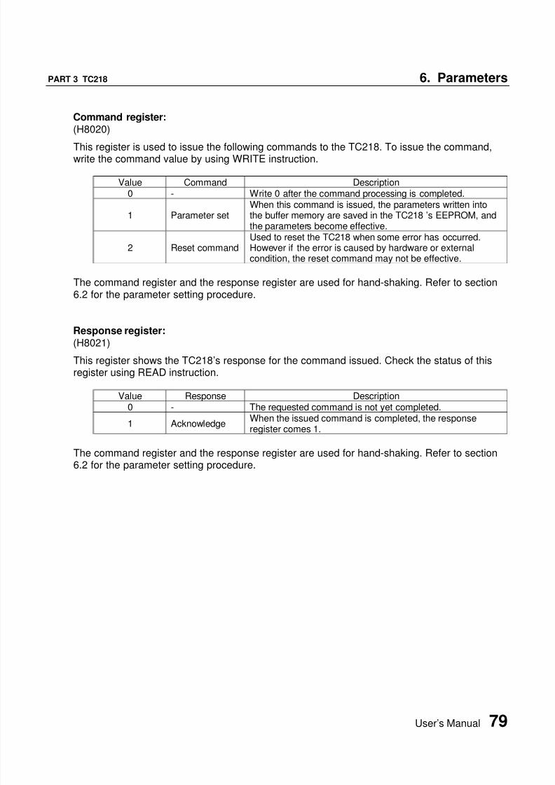
8/8/2019 T2 Analog I-O Modules
http://slidepdf.com/reader/full/t2-analog-i-o-modules 81/88
User’s Manual 79
PART 3 TC218 6. Parameters
Command register:(H8020)
This register is used to issue the following commands to the TC218. To issue the command,write the command value by using WRITE instruction.
Value Command Description0 - Write 0 after the command processing is completed.
1 Parameter setWhen this command is issued, the parameters written intothe buffer memory are saved in the TC218 ’s EEPROM, andthe parameters become effective.
2 Reset commandUsed to reset the TC218 when some error has occurred.However if the error is caused by hardware or externalcondition, the reset command may not be effective.
The command register and the response register are used for hand-shaking. Refer to section6.2 for the parameter setting procedure.
Response register:(H8021)
This register shows the TC218’s response for the command issued. Check the status of thisregister using READ instruction.
Value Response Description0 - The requested command is not yet completed.
1 AcknowledgeWhen the issued command is completed, the responseregister comes 1.
The command register and the response register are used for hand-shaking. Refer to section6.2 for the parameter setting procedure.

8/8/2019 T2 Analog I-O Modules
http://slidepdf.com/reader/full/t2-analog-i-o-modules 82/88
80 Analog I/O Modules (AD268 / DA264 / TC218)
6. Parameters PART 3 TC218
Analog input actual value:(H8028 to H802F)
These data show the original A/D conversion data before processing the gain and offsetcalibration.
Module status:(H8030 to H8037)
These data show the TC218’s operation status.
Bit position → F E D C B A 9 8 7 6 5 4 3 2 1 0
0 0 0 0 0
Bit Name Description0 to 2 Input type Shows the input type.
000 (0) = Type K thermocouple001 (1) = Type J thermocouple010 (2) = Type E thermocouple
101 (5) = ±100mV3 to 6 - Reserved
7 Input type settingerror
1 when the input type designation is invalid.
8 Burnout detection 1 when thermocouple burnout is detected.9 Input limit 1 when the A/D conversion data is limited because of the range
over.A MPU error 1 when the TC218’s processor is not normal.B ROM status 1 when the TC218’s EEPROM is not normal.C DP-RAM status 1 when the TC218’s DP-RAM (buffer memory) is not normal.D - ReservedE External 24V error 1 when the external 24Vdc is not normal.F Initializing 1 during the TC218 is in initialization process.

8/8/2019 T2 Analog I-O Modules
http://slidepdf.com/reader/full/t2-analog-i-o-modules 83/88
User’s Manual 81
PART 3 TC218 6. Parameters
6.2 Parameter setting procedure
When you change the TC218 parameters, such as input type settings, gain/offset calibrationsand averaging times, use the following procedure.
Step (1)
Write the value "0" into the command register of the TC218 buffer memory (address H8020)by WRITE instruction.
H8020 Command register ← Write 0
Step (2)
Write the parameter data into the buffer memory (addresses H8000 to H801F) by WRITEinstruction. Be sure to write all the 32 words in batch.For thermocouple, write the default value for the gain (32000) and the offset (0).
H8000 Gain for channel 1H8001 Gain for channel 2
: :
H801F Input type for channel 8
← Write the parameter data (32 words)
Step (3)
Write the value "1" into the command register (address H8020) by WRITE instruction.
H8020 Command register ← Write 1
Step (4)
Wait until the data of the response register (address H8021) comes "1". Check the data byREAD instruction.
H8021 Response register Check if it comes 1
Step (5)Write the value "0" into the command register (address H8020) by WRITE instruction.
H8020 Command register ← Write 0
When the above steps are finished and the module status (addresses H8030 to H8037) showsno error, the parameter setting procedure is completed. The parameters are effective and theyhave been saved in the TC218's EEPROM.
Note) After you write the parameters into the TC218, turn off power and on again.

8/8/2019 T2 Analog I-O Modules
http://slidepdf.com/reader/full/t2-analog-i-o-modules 84/88
82 Analog I/O Modules (AD268 / DA264 / TC218)
6. Parameters PART 3 TC218
6.3 Sample program for setting the parameters
A sample program to set the parameters is shown below.This is an example to set the input type as the type J thermocouple (type = 1) for each channel.In this sample program, it is assumed that he TC218 is allocated to XW000 to XW007.
For details of READ and WRITE instructions, refer to the T-series Instruction Set manual.
(Main program)
In this sample program, the rung 1 is activated at the beginning of RUN mode (at the secondscan) automatically. The input type is set to the type J thermocouple for all 8 channels.When the parameter setting process is completed, the flags R1000 to R1002 are returned toOFF.
For reading the parameters from the TC218, there is no special procedure. Simply read the
data from the TC218’s buffer memory by using READ instruction.
Step (1):Writes 0 into thecommandregister (H8020).
Step (2):Writes parameters.
• Gain = 32000
• Offset = 0
• Average = 1
• Type = 1 (type J)Total 32 wordsstarting with
Step (3):Writes 1 into thecommandregister (H8020).
Step (4):Waits until theresponseregister (H8021)comes 1.
Step (5):Writes 0 into thecommand
register (H8020)to return to initialstate.
(H8020)
(H8000)
(H8020)
(H8021)
(H8020)
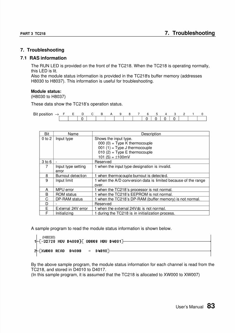
8/8/2019 T2 Analog I-O Modules
http://slidepdf.com/reader/full/t2-analog-i-o-modules 85/88
User’s Manual 83
PART 3 TC218 7. Troubleshooting
7. Troubleshooting
7.1 RAS informationThe RUN LED is provided on the front of the TC218. When the TC218 is operating normally,this LED is lit.Also the module status information is provided in the TC218‘s buffer memory (addressesH8030 to H8037). This information is useful for troubleshooting.
Module status:(H8030 to H8037)
These data show the TC218’s operation status.
Bit position → F E D C B A 9 8 7 6 5 4 3 2 1 0
0 0 0 0 0
Bit Name Description0 to 2 Input type Shows the input type.
000 (0) = Type K thermocouple001 (1) = Type J thermocouple010 (2) = Type E thermocouple
101 (5) = ±100mV3 to 6 - Reserved
7 Input type settingerror
1 when the input type designation is invalid.
8 Burnout detection 1 when thermocouple burnout is detected.9 Input limit 1 when the A/D conversion data is limited because of the range
over.A MPU error 1 when the TC218’s processor is not normal.B ROM status 1 when the TC218’s EEPROM is not normal.C DP-RAM status 1 when the TC218’s DP-RAM (buffer memory) is not normal.D - ReservedE External 24V error 1 when the external 24Vdc is not normal.F Initializing 1 during the TC218 is in initialization process.
A sample program to read the module status information is shown below.
By the above sample program, the module status information for each channel is read from theTC218, and stored in D4010 to D4017.(In this sample program, it is assumed that the TC218 is allocated to XW000 to XW007)
(H8030)

8/8/2019 T2 Analog I-O Modules
http://slidepdf.com/reader/full/t2-analog-i-o-modules 86/88
84 Analog I/O Modules (AD268 / DA264 / TC218)
7. Troubleshooting PART 3 TC218
7.2 Troubleshooting
The table below shows the trouble and its remedy.
Trouble Modulestatus info
LED Module operation Cause Remedy
Input typesetting error
Bit 7 is ON ON(if the erroroccurs in allchannels, itis OFF)
The error channelstops theconversion. The A/Dconversion data is 0.
Invalid input typeparameter was set.
Set the correctinput typeparameter.
Thermocoupleburnout
Bit 8 is ON ON The A/D conversiondata of the channelis 32767 (H7FFF).
The thermocoupleinput wire becomesopen.
Check thethermocouple.
Analog signallimit over
Bit 9 is ON ON The A/D conversiondata of the channelis limited by the limitvalue.
Analog input signalis out of the range.
Check the signalsource (sensor).
MPU error Bit A is ON OFF The A/D conversionis stopped.
Internal processoroperation is notnormal.
Execute resetcommand, orcycle power offand on.
ROM error Bit B is ON OFF The A/D conversionis stopped.
EEPROM dataerror is detected.
Cycle power offand on.
DP-RAM error Bit C is ON OFF The A/D conversionis stopped.
Buffer memoryaccess error isoccurred.
Cycle power offand on.
External 24Verror Bit E is ON OFF The A/D conversionis stopped. Internal ±15Vvoltage is notnormal.
Check theexternal 24Vdcpower supply.

8/8/2019 T2 Analog I-O Modules
http://slidepdf.com/reader/full/t2-analog-i-o-modules 87/88
User’s Manual 85

8/8/2019 T2 Analog I-O Modules
http://slidepdf.com/reader/full/t2-analog-i-o-modules 88/88
TOSHIBA CORPORATIONIndustrial Equipment Department