SYSTEM SIMULATION LABORATORY MANUAL … Sir C.R. Reddy College of Engg. Eluru – 7 I/II M.Tech...
40
1 Sir C.R. Reddy College of Engg. Eluru – 7 I/II M.Tech (VLSI), II-SEM :: SS Lab Manual SYSTEM SIMULATION LABORATORY MANUAL FOR I / II M.TECH VLSI DESIGN (ECE) II - SEMESTER DEPT. OF ELECTRONICS AND COMMUNICATION ENGINEERING SIR C.R.REDDY COLLEGE OF ENGINEERING ELURU – 534 007
Transcript of SYSTEM SIMULATION LABORATORY MANUAL … Sir C.R. Reddy College of Engg. Eluru – 7 I/II M.Tech...

1
Sir C.R. Reddy College of Engg. Eluru – 7 I/II M.Tech (VLSI), II-SEM :: SS Lab Manual
SYSTEM SIMULATION LABORATORY MANUAL
FOR I / II M.TECH VLSI DESIGN (ECE)
II - SEMESTER
DEPT. OF ELECTRONICS AND COMMUNICATION ENGINEERING
SIR C.R.REDDY COLLEGE OF ENGINEERING
ELURU – 534 007

2
Sir C.R. Reddy College of Engg. Eluru – 7 I/II M.Tech (VLSI), II-SEM :: SS Lab Manual
SYSTEM SIMULATION LABORATORY MANUAL
FOR I / II M.TECH VLSI DESIGN (ECE)
II - SEMESTER
LIST OF EXPERIMENTS
Experiments shall be carried out by using Mentor Graphics/Cadence Tools
1. CMOS INVERTER
2. TWO INPUT CMOS NAND GATE
3. TWO INPUT CMOS NOR GATE
4. CMOS TRANSMISSION GATE
5. TWO INPUT AND GATE
6. TWO INPUT OR GATE
7. DIFFERENTIAL AMPLIFIER
8. COMMON SOURCE AMPLIFIER
9. COMMON DRAIN AMPLIFIER
10. 2X1 MULTIPLEXER
3
Sir C.R. Reddy College of Engg. Eluru – 7 I/II M.Tech (VLSI), II-SEM :: SS Lab Manual
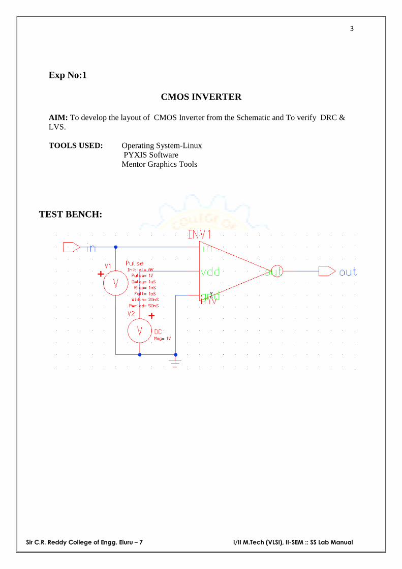
Exp No:1
CMOS INVERTER
AIM: To develop the layout of CMOS Inverter from the Schematic and To verify DRC & LVS. TOOLS USED: Operating System-Linux PYXIS Software Mentor Graphics Tools
TEST BENCH:

4
Sir C.R. Reddy College of Engg. Eluru – 7 I/II M.Tech (VLSI), II-SEM :: SS Lab Manual
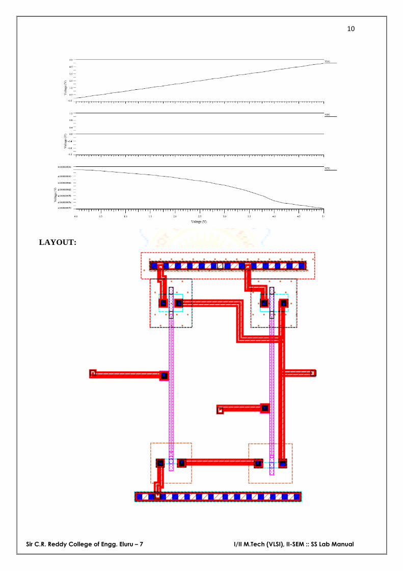
TIMING DIAGRAM:
LAYOUT:

5
Sir C.R. Reddy College of Engg. Eluru – 7 I/II M.Tech (VLSI), II-SEM :: SS Lab Manual
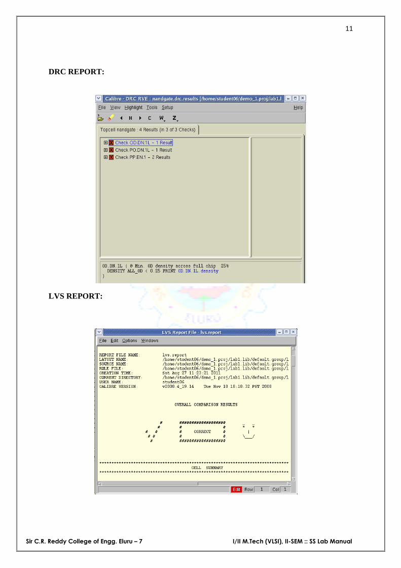
DRC REPORT:

6
Sir C.R. Reddy College of Engg. Eluru – 7 I/II M.Tech (VLSI), II-SEM :: SS Lab Manual
LVS REPORT:

7
Sir C.R. Reddy College of Engg. Eluru – 7 I/II M.Tech (VLSI), II-SEM :: SS Lab Manual
RESULT: Hence developed the schematic and layout. Verified the DRC and LVS report. is done.

8
Sir C.R. Reddy College of Engg. Eluru – 7 I/II M.Tech (VLSI), II-SEM :: SS Lab Manual
Exp No:2
TWO INPUT NAND GATE
AIM: To develop the layout of Two input CMOS NAND gate from the Schematic and to verify DRC & LVS . TOOLS USED: Operating System-Linux IC Studio Design Architecture-IC-V2008.1 SCHEMATIC:
SYMBOL:

9
Sir C.R. Reddy College of Engg. Eluru – 7 I/II M.Tech (VLSI), II-SEM :: SS Lab Manual
TEST BENCH:
NETLIST TIMING DIAGRAM:
10
Sir C.R. Reddy College of Engg. Eluru – 7 I/II M.Tech (VLSI), II-SEM :: SS Lab Manual
LAYOUT:
11
Sir C.R. Reddy College of Engg. Eluru – 7 I/II M.Tech (VLSI), II-SEM :: SS Lab Manual
DRC REPORT:
LVS REPORT:

12
Sir C.R. Reddy College of Engg. Eluru – 7 I/II M.Tech (VLSI), II-SEM :: SS Lab Manual
RESULT:Hence developed the schematic and layout.verified the DRC and LVS report done.
13
Sir C.R. Reddy College of Engg. Eluru – 7 I/II M.Tech (VLSI), II-SEM :: SS Lab Manual
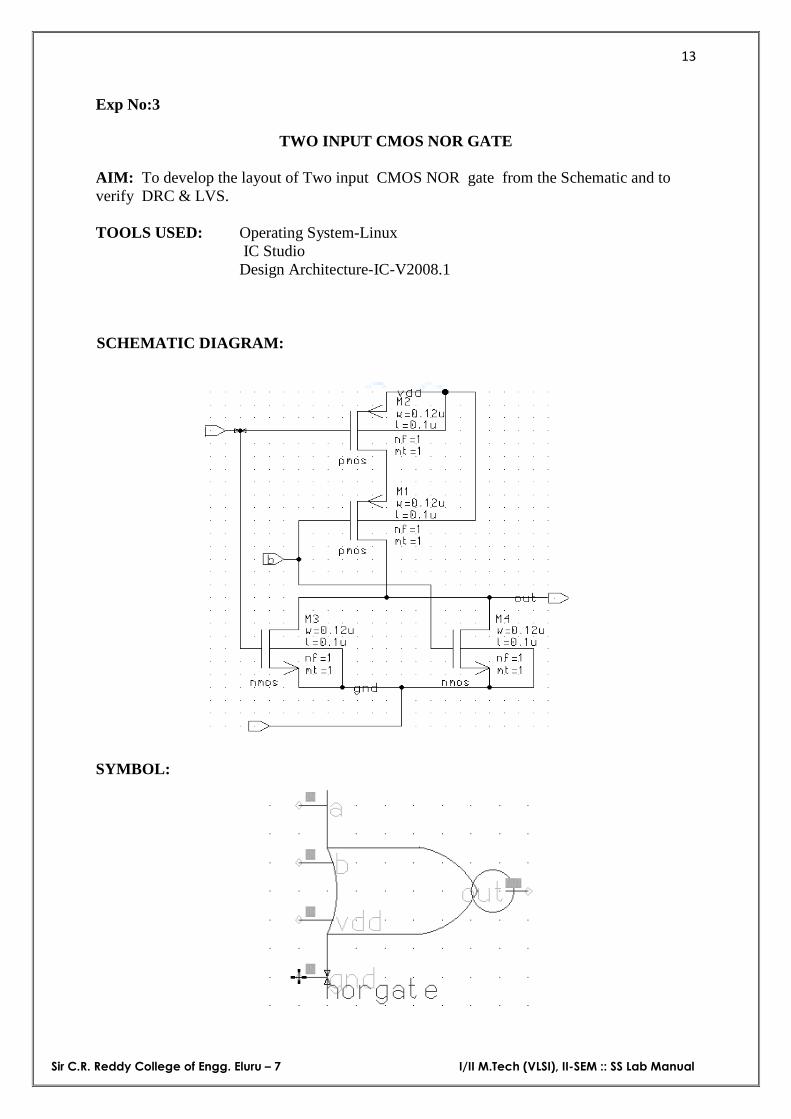
Exp No:3
TWO INPUT CMOS NOR GATE
AIM: To develop the layout of Two input CMOS NOR gate from the Schematic and to verify DRC & LVS. TOOLS USED: Operating System-Linux IC Studio Design Architecture-IC-V2008.1
SCHEMATIC DIAGRAM:
SYMBOL:

14
Sir C.R. Reddy College of Engg. Eluru – 7 I/II M.Tech (VLSI), II-SEM :: SS Lab Manual
TEST BENCH:
TIMING DIAGRAM:
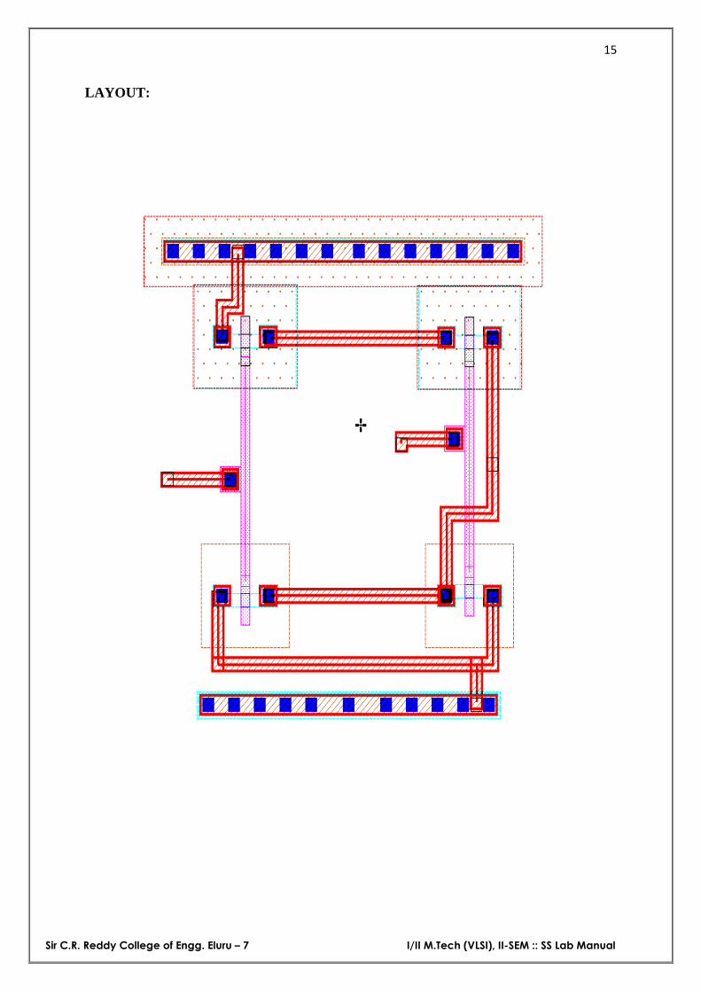
15
Sir C.R. Reddy College of Engg. Eluru – 7 I/II M.Tech (VLSI), II-SEM :: SS Lab Manual
LAYOUT:

16
Sir C.R. Reddy College of Engg. Eluru – 7 I/II M.Tech (VLSI), II-SEM :: SS Lab Manual
DRC REPORT:
LVS REPORT:

17
Sir C.R. Reddy College of Engg. Eluru – 7 I/II M.Tech (VLSI), II-SEM :: SS Lab Manual
RESULT: Hence developed the schematic and layout.Verified the DRC and LVS report is done.

18
Sir C.R. Reddy College of Engg. Eluru – 7 I/II M.Tech (VLSI), II-SEM :: SS Lab Manual
Exp No:4 CMOS TRANSMISSION GATE
AIM: To develop the layout of CMOS Transmission gate from the Schematic and to verify DRC & LVS. TOOLS USED: Operating System-Linux IC Studio Design Architecture-IC-V2008.1 SCHEMATIC DIAGRAM:

19
Sir C.R. Reddy College of Engg. Eluru – 7 I/II M.Tech (VLSI), II-SEM :: SS Lab Manual
TEST BENCH:
TIMING DIAGRAM:
LAYOUT:

20
Sir C.R. Reddy College of Engg. Eluru – 7 I/II M.Tech (VLSI), II-SEM :: SS Lab Manual
DRC REPORT:

21
Sir C.R. Reddy College of Engg. Eluru – 7 I/II M.Tech (VLSI), II-SEM :: SS Lab Manual
LVS REPORT:
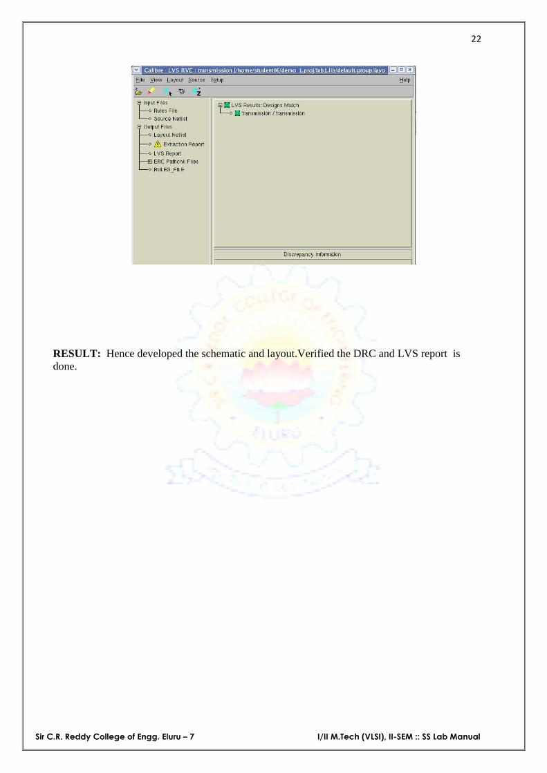
22
Sir C.R. Reddy College of Engg. Eluru – 7 I/II M.Tech (VLSI), II-SEM :: SS Lab Manual
RESULT: Hence developed the schematic and layout.Verified the DRC and LVS report is done.

23
Sir C.R. Reddy College of Engg. Eluru – 7 I/II M.Tech (VLSI), II-SEM :: SS Lab Manual
Exp No:5
TWO INPUT AND GATE
AIM: To develop the schematic for two input AND gate and to observe the timing waveforms. TOOLS USED: Operating system -linux
Xmangaer Enterprise 3
SCHEMATIC DIAGRAM:

24
Sir C.R. Reddy College of Engg. Eluru – 7 I/II M.Tech (VLSI), II-SEM :: SS Lab Manual
SYMBOL:
Test bench:

25
Sir C.R. Reddy College of Engg. Eluru – 7 I/II M.Tech (VLSI), II-SEM :: SS Lab Manual
TIMING DIAGRAM:
NETREPORT:
Number of cells: 4
Number of primitive instances: 7
NETLIST:
* MAIN CELL: Component pathname : /home/student0X/andgate
* MP2 N$617 IN2 VDD VDD p L=2u W=5u M=1
MP1 N$617 IN1 VDD VDD p L=2u W=5u M=1
MN2 N$619 IN2 GND VSS n L=2u W=5u M=1
MN1 N$617 IN1 N$619 VSS n L=2u W=5u M=1
MN OUT N$617 GND VSS n L=2u W=5u M=1
MP OUT N$617 VDD VDD p L=2u W=5u M=1
V1 VDD GND DC 5V .end
RESULT: Hence the schematic for Two input AND gate designed and observed the simulation results.
26
Sir C.R. Reddy College of Engg. Eluru – 7 I/II M.Tech (VLSI), II-SEM :: SS Lab Manual
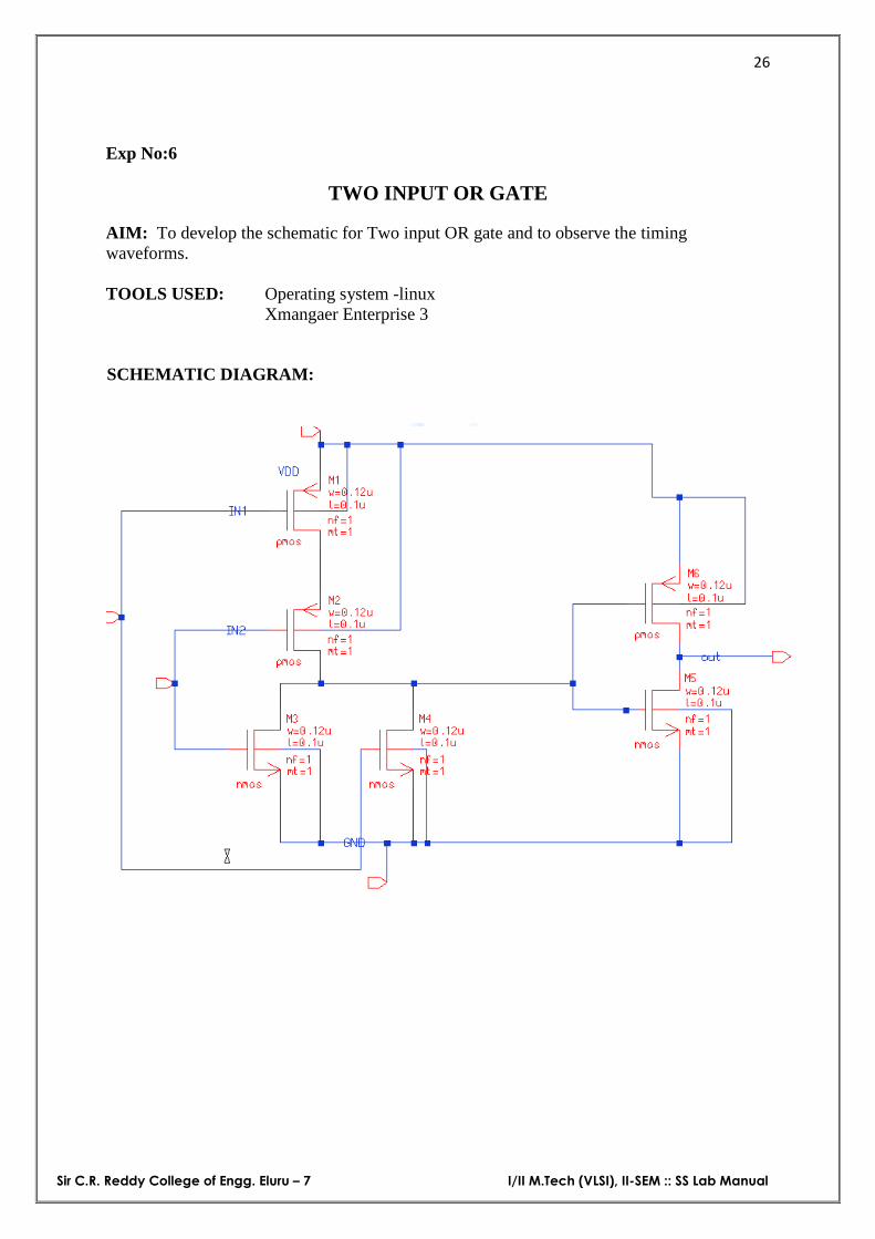
Exp No:6
TWO INPUT OR GATE
AIM: To develop the schematic for Two input OR gate and to observe the timing waveforms. TOOLS USED: Operating system -linux
Xmangaer Enterprise 3
SCHEMATIC DIAGRAM:

27
Sir C.R. Reddy College of Engg. Eluru – 7 I/II M.Tech (VLSI), II-SEM :: SS Lab Manual
SYMBOL:
Test bench:

28
Sir C.R. Reddy College of Engg. Eluru – 7 I/II M.Tech (VLSI), II-SEM :: SS Lab Manual
TIMING DIAGRAM:
NETREPORT:
Number of cells: 2
Number of primitive instances: 1
NETLIST:
* MAIN CELL: Component pathname : /home/student09/or
* OR2__OR1 A B OUT
*.end
RESULT:
Hence the schematic for Two input OR gate designed and observed the simulation results.

29
Sir C.R. Reddy College of Engg. Eluru – 7 I/II M.Tech (VLSI), II-SEM :: SS Lab Manual
Exp No:7
Common Source
AIM: To develop the schematic for current source and to observe the timing waveforms. TOOLS USED: Operating system -linux
Xmangaer Enterprise 3
SCHEMATIC DIAGRAM:

30
Sir C.R. Reddy College of Engg. Eluru – 7 I/II M.Tech (VLSI), II-SEM :: SS Lab Manual
Test Bench:
TIMING DIAGRAM:

31
Sir C.R. Reddy College of Engg. Eluru – 7 I/II M.Tech (VLSI), II-SEM :: SS Lab Manual
NET REPORT: Number of cells: 5 Number of primitive instances: 5 NETLIST: * MAIN CELL: Component pathname : /home/student0X/currentmirror *V1 VDD GROUND DC 1V R1 VCC OUT MODEL 10k M3 OUT N$2 GROUND GROUND NCH L=0.35u W=1.4u M=1 M2 N$2 IN VCC VCC PCH L=0.35u W=1.4u M=1 M1 GROUND N$2 N$2 GROUND NCH L=0.35u W=1.4u M=1* .end
RESULT:
Hence the schematic for current mirror designed and observed the timing waveforms .

32
Sir C.R. Reddy College of Engg. Eluru – 7 I/II M.Tech (VLSI), II-SEM :: SS Lab Manual
Exp No:8
Common Drain
AIM: To develop the schematic for common drain and to observe the timing waveforms. TOOLS USED: Operating system -linux
Xmangaer Enterprise 3
SCHEMATIC DIAGRAM:

33
Sir C.R. Reddy College of Engg. Eluru – 7 I/II M.Tech (VLSI), II-SEM :: SS Lab Manual
TIMING DIAGRAM:

34
Sir C.R. Reddy College of Engg. Eluru – 7 I/II M.Tech (VLSI), II-SEM :: SS Lab Manual
NET REPORT: Number of cells: 5 Number of primitive instances: 5
RESULT:
Hence the schematic for common drain designed and observed the timing waveforms .

35
Sir C.R. Reddy College of Engg. Eluru – 7 I/II M.Tech (VLSI), II-SEM :: SS Lab Manual
Exp No: 9
Differential Ampilfier
AIM: To develop the schematic for Differential Ampilfier and to observe the timing waveforms.
TOOLS USED: Operating system -linux
Xmangaer Enterprise 3
SCHEMATIC DIAGRAM:

36
Sir C.R. Reddy College of Engg. Eluru – 7 I/II M.Tech (VLSI), II-SEM :: SS Lab Manual
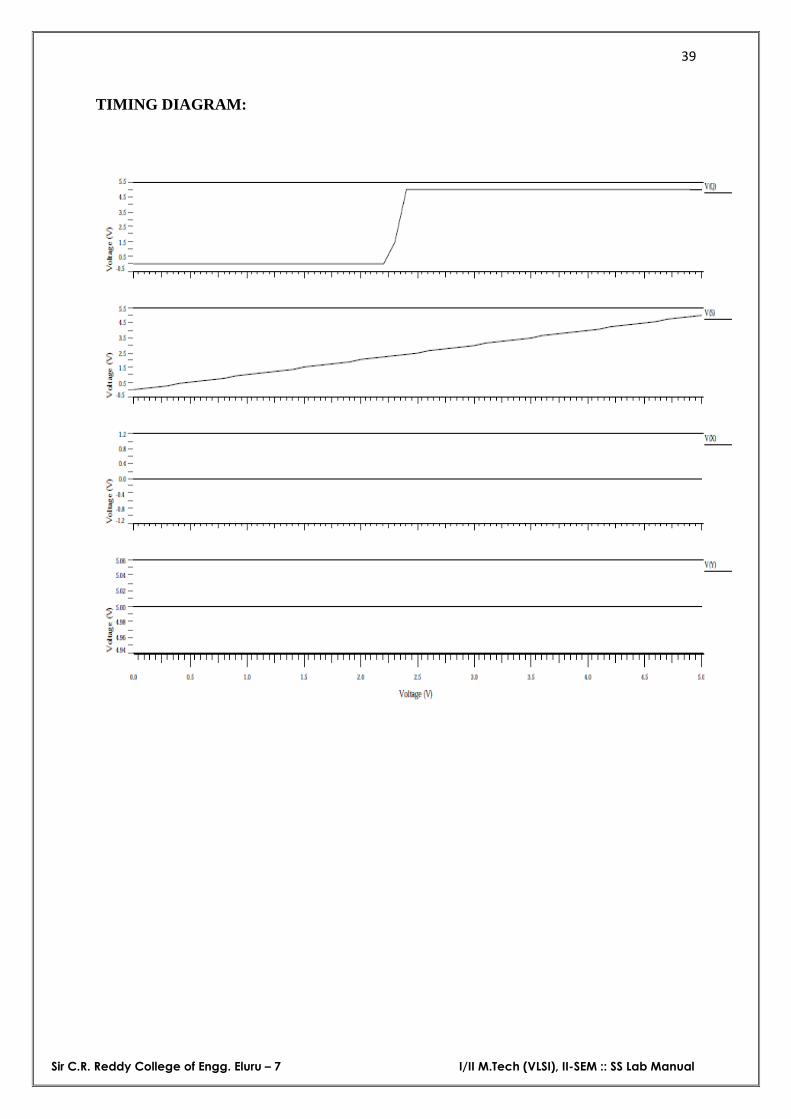
TIMING DIAGRAM:
37
Sir C.R. Reddy College of Engg. Eluru – 7 I/II M.Tech (VLSI), II-SEM :: SS Lab Manual
NET REPORT: Number of cells: 5 Number of primitive instances: 5
RESULT:
Hence the schematic for Differential Ampilfier designed and observed the timing waveforms .

38
Sir C.R. Reddy College of Engg. Eluru – 7 I/II M.Tech (VLSI), II-SEM :: SS Lab Manual
Exp No:10 Date:
2x1 MUTIPLEXER
AIM: To Develop The Schematic For The 2x1 Mutiplexer and verify the simulation results
TOOLS USED: Operating System-Linux PYXIS Software Mentor Graphics Tools
SCHEMATIC DIAGRAM:
39
Sir C.R. Reddy College of Engg. Eluru – 7 I/II M.Tech (VLSI), II-SEM :: SS Lab Manual
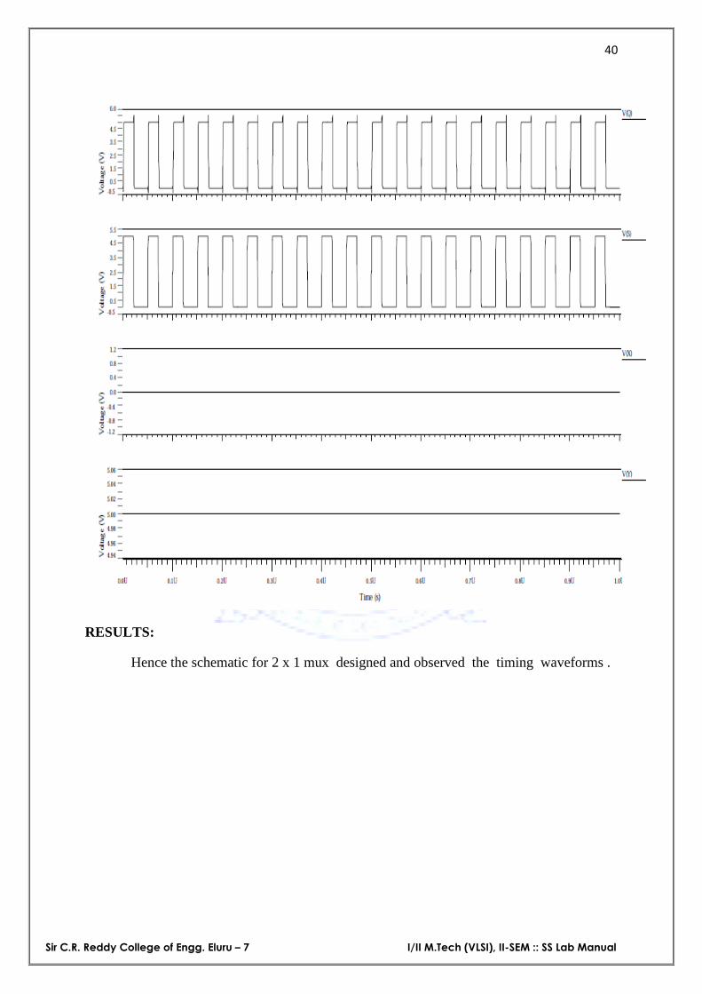
TIMING DIAGRAM:
40
Sir C.R. Reddy College of Engg. Eluru – 7 I/II M.Tech (VLSI), II-SEM :: SS Lab Manual
RESULTS:
Hence the schematic for 2 x 1 mux designed and observed the timing waveforms .


![M.tech II Sem Syllabus[1]](https://static.fdocuments.us/doc/165x107/577cb4171a28aba7118c4c56/mtech-ii-sem-syllabus1.jpg)