


System scaling: the next frontier for a new era of electronic systems
60
Transcript of System scaling: the next frontier for a new era of electronic systems

11Chip Scale Review September • October • 2015 [ChipScaleReview.com]
CONTENTSSeptember • October 2015
Volume 19, Number 5
Chip Scale R
eviewS
eptember • O
ctober 2015 Volume 19, N
umber 5
ChipScaleR
eview.com
The Future of Semiconductor PackagingV olume 19, N umb er 5 Septemb er • Octob er 2 015
• Out of this world electronics packaging
• Package- level integration of ME MS in IoT devices
• Thermocompression bonding for fl ip-chip technology
• Bond tester study of CSP reliability through bump analysis
• System scaling: the next frontier for a new era of electronic systems
• Performance of optimized lithography tools in advanced packaging applications
Packaging IC s to survive the automotive environmentPage 18
DEPARTMENTS
Electronics packaging is constantly evolving to meet the demands for automotive, medical and consumer products that require improved per formance. Automot ive elect ronics are among the most demanding in harsh environments and must meet higher standards in order to ensure reliability and safety. Progressive packaging technologies from leaded to surface mount to MEMS, 3D, and die-level packaging will continue to place even more stringent demands on IC packages in these automotive applications. Photo courtesy of Amkor Technology®
Technology Trends System scaling: the next frontier for a new era of electronic systemsRao TummalaGeorgia Institute of Technology
5
Market Trends Package-level integration of MEMS motion sensors in IoT devicesStephen BreitCoventor, Inc.
10
Guest Editorial Photonics integration and packaging gaining tractionHiren D. Thacker OracleStefan Weiss II-VI Laser Enterprise
15
Advertiser Index, Advertising Sales 56
Advanced solutions to meet your application needs now and for the future...
MEMS and sensors for microphones, gyroscopes,accelerometers and pressure, humidity/temperature,fingerprint, light, infrared and fusion sensors
Packages not shown at actual size. © 2015 Amkor Technology, Inc.
Visit Amkor Technology online for the most current product information
www.amkor.com
MLF®
LGA
CavityMEMS
Enabling a Smart Connected World
MEMS

22 Chip Scale Review September • October • 2015 [ChipScaleReview.com]
33Chip Scale Review September • October • 2015 [ChipScaleReview.com]
CONTENTSVolume 19, Number 5
The International Magazine for Device and Wafer-level Test, Assembly, and Packaging Addressing
High-density Interconnection of Microelectronic IC's including 3D packages, MEMS, MOEMS,RF/Wireless, Optoelectronic and Other
Wafer-fabricated Devices for the 21st Century.
STAFFKim Newman [email protected] Michaels Managing Director/[email protected] Vogler Senior Technical [email protected]
CONTRIBUTING EDITORSDr. Thomas Di Stefano Contributing Editor - [email protected] H. Grace Contributing Editor - [email protected] Mirabito Contributing Editor - [email protected]. Ephraim Suhir Contributing - Editor - [email protected]
EDITORIAL ADVISORSDr. Andy Mackie (Chair) Indium CorporationDr. Rolf Aschenbrenner Fraunhofer InstituteDr. Thomas Di Stefano Centipede SystemsJoseph Fjelstad Verdant ElectronicsDr. Arun Gowda GE Global ResearchDr. John Lau ASM Pacifi c TechnologyDr. Venky Sundaram Georgia Institute of Technology-3D Systems Packaging Research CenterDr. Leon Lin Tingyu National Center for Advanced Packaging (NCAP China)Francoise von Trapp 3D InCites
SUBSCRIPTION--INQUIRIESChip Scale ReviewAll subscription changes, additions, deletions to any and all subscriptions should be made by email only to [email protected]
Advertising Production Inquiries:Kim [email protected]
Copyright © 2015 Haley Publishing Inc.Chip Scale Review (ISSN 1526-1344) is a registered trademark ofHaley Publishing Inc. All rights reserved.
Subscriptions in the U.S. are available without charge to qualifi edindividuals in the electronics industry. Subscriptions outside of the $225 peryear to other countries. In the U.S. subscriptions by fi rst class mailare $125 per year.
Chip Scale Review, (ISSN 1526-1344), is published six times ayear with issues in January-February, March-April, May-June, July-August, September-October and November-December. Periodicalpostage paid at Los Angeles, Calif., and additional offi ces.
POSTMASTER: Send address changes to Chip Scale Reviewmagazine, P.O. Box 9522, San Jose, CA 95157-0522
Printed in the United States
FEATURE ARTICLES
Packaging ICs to survive the automotive environmentPrasad Dhond Amkor Technology® 18
Bond tester study of CSP reliability through bump analysisEvstatin Krastev, Ian Christopher Mayes, Chan Myat, Armin Struwe Nordson DAGERene P. Zingg Zinan GmbH, Ricardo Geelhaar PacTech GmbH
41
Out of this world electronics packagingAndrew A. Shapiro Jet Propulsion Laboratory, California Institute of Technology
25
Using cost modeling to make better design decisionsAmy Palesko SavanSys Solutions LLC 37
Thermocompression bonding for flip-chip technologyJohn H. Lau, Li Ming, Nelson Fan, Ringo TseASM Pacifi c Technology Ltd.
30
Performance of optimized lithography tools and materials in advanced packaging applicationsKeith Best Rudolph Technologies, Inc.
49
Solving delamination in lead frame-based packagesRongwei Zhang, Yong Lin, Abram Castro Texas Instruments Inc. 44
New choices for low-temperature dielectric fi lmsRobert L. Hubbard Lambda Technologies, Inc. 51
www.e-tec.com
E-tec Interconnect AG
E-tec Interconnect is pleased to present its new Clamshell Open Top Socket• High reliability
• High frequency
•Also pluggable into adapter MiniGridSocket series (see E-tec catalog TS01)
•
E-tec Interconnect is E-tec Interconnect is pleased to present its pleased to present its
NEW in the Test Socket World :
E-tec Inserat Socket 2015 117x123mm US.indd 1 18.06.15 10:03

55Chip Scale Review September • October • 2015 [ChipScaleReview.com]
System scaling: the next frontier for a new era of electronic systemsBy Rao Tummala [Georgia Institute of Technology]
hat made electronics t h e l a r g e s t g l o b a l i n d u s t r y a t $ 1 . 4 T has been the singular
focus on t rans is tor sca l ing . The s e m i c o n d u c t o r , p a c k a g i n g a n d sys t ems l andscape , however, i s changing dramatically. For example, on one hand , ICs , f o r t he mos t part , are becoming commodities, providing much lower profit margins than ever before, thereby leading to industry consolidat ion to less than five manufacturing companies worldwide within the next decade. In addition, the cost and complexity of t rans i s tor sca l ing i s g rowing exponentially. There is no longer a cost reduction as the next node is introduced with higher transistor density. It’s becoming apparent that transistor scaling is slowing down as well, taking much longer from node to node than previous transitions. In addition, there are two main technical problems with t ransis tor scal ing to form the most advanced ICs: in the front end, i t is the dielectric leakage, and in the back end, it is the interconnect performance. So-called RC delays, known to be a problem for two decades , a re the reason for the performance problem. The average delay due to high-resistance copper interconnections increases by almost 50% from the 45nm to the 7nm node. On top of that, design and process complexity of ICs beyond 14nm go up exponentially, adding to the yield and cost issues. Can system scaling enable better devices?
The second challenge concerns the packaging of devices. Most of the current packaging is to package s i n g l e d e v i c e s , s u c h a s I n t e l ’s processors for PCs and lap tops . Tradi t iona l packaging i s adding
minimal value to these applications by becoming cos t ly, bu lky, and in addition, i t detracts from chip rel iabil i ty. In this need, the best packaging seems to be no packaging and assembly at all. This is clearly one of the drivers for chip-first or embedded packaging. Can system scaling address these challenges?
The third landscape change is about the emerging electronic systems. The driving engines for electronic systems are changing dramatically to small systems, such as smartphones, and ultra-small systems such as wearables, like the Apple watch that promise to perform every imaginable heterogeneous function.
On the other extreme, l a rg e s y s t e m s s u c h a s automotive, are entering a n e w e r a o f s e l f -d r i v i n g , s m a r t p h o n e -like infotainment within t h e c a r , a s w e l l a s i n al l -electr ic cars . These systems perform dozens of heterogeneous functions that include digital and wireless communications; wireless sensing, stereo cameras, mm-wave electronics, high-bandwidth electronics or photonics for data processing from 100s of sensors and with data security; and high-power and high-temperature electronics for all-electric cars.
Integration of the above mentioned heterogeneous functions is more than transistor scaling and integration by Moore's Law, and a lot More than Moore's Law (MTM) with stacked heterogeneous integration of ICs, or system-in-package (SiP). Georgia Tech calls this next era of integration S y s t e m M o o r e ' s L a w ( S M ) b y system scaling for complete system
integration of electronic systems such as smartphones, wearables, Internet of Things (IoTs), automotive electronics, and cloud computing.
System scaling R&D at Georgia TechThe end goal of system scaling is
to enable entire system-on-one single package (SOP) in contrast to system-on-chip (SoC) by transistor scaling alone, with a market size as big as all the electronics to date. The progress in system scaling is illustrated in Figure 1 and shows the gap between transistor scaling as measured by node in nanometers, and system scaling, as
measured by off-chip interconnection pitch in microns over the last 40 years.
Georgia Tech has put together a global industry consortium it calls SSI (System Scaling and Integration), to explore and develop the System M o o r e c o n c e p t f r o m d e s i g n t o demonstration involving 50 integrated device manufacturers (IDMs), original equipment manufacturers (OEMs), outsourced semiconductor assembly and test services (OSATs), package foundries, and package materials and tools suppliers.
Georgia Tech is pioneering glass-based device and systems packaging
W
TECHNOLOGY TRENDS
Figure 1: Gap between transistor scaling and system scaling.

66 Chip Scale Review September • October • 2015 [ChipScaleReview.com]
as the system scaling platform. Table 1 shows the comparison of glass against single-crystal Si, polycrystalline Si, organic laminate, metal and ceramic packaging. Ultra-thin glass processed as an ultra-large panel (up to 12” x 18”) seems to have the best potential to be the system scaling platform with the highest electrical performance, lowest cost, and highest reliability. Such a platform can end up with the highest heterogeneous functionality at the lowest cost in the smallest size that serves both small systems, such as smartphones, and large systems, such as automotive electronics and cloud computing. The reasons for this are many that include the following:
• Outstanding electrical properties: ultra-low electrical loss, low-dielectric constant and ultra-high resistivity;
• Outstanding mechanical properties: intrinsic high strength and high modulus for low warpage;
• Excellent thermal properties: thermal coefficient of expansion (TCE) matching Si, GaN, SiC or GaAs, excellent thermal insulation and excellent thermal conductivity locally with low-cost copper through-vias, slugs and ground planes;
• Excellent chemical properties: no moisture absorption and resistance to chemical processing;
• Excellent Si-like surface finish:
for direct metallization to sub-micron lithography;
• Large-area processing: available in large and thin sizes for large panel and roll-to-roll processing; and
• High-throughput through-vias: many high-throughput processes for via holes and via fi lling.
The System Moore architecture concept i s a 3D system package b a s e d o n s y s t e m s c a l i n g a n d heterogeneous integration (Figure 2). The fundamental technologies behind this architecture, now and in the near future, are ultra-thin glass, typically 30 microns in thickness; TSV-like vias, typically 5 microns in diameter with a 10-50 micron pitch; and redistribution layer (RDL) with 1-3 micron ground
rules so as to end up with an off-chip interconnection pitch in the 5-30 microns range. Any active or passive c o m p o n e n t s i n c l u d i n g m e m o r y stacks, logic processors, WLAN, and LTE modules can be assembled and interconnected on both sides. In this approach for the first time, any two active or passive system components can be interconnected with less than a 100 micron interconnect length.
The fundamentals of SSI with glass packaging are many, and include:
• Short interconnect length for highest performance;
• Ultra-low loss substrates and dielectrics for minimum power consumption in interconnections;
• Ultra-low loss substrates and dielectrics for high-frequency (mm-wave), and data-secure communications;
• Low-dielectric constant dielectrics for high signal speed;
• Through TSV-like vias at fi ne-pitch for double-side interconnections and assembly of actives and passives to form 3D packages with the same TSV pitch for miniaturization and performance;
• Thick Cu ground planes and large Cu through-vias or slugs for high-thermal dissipation;
• L a r g e - p a n e l ( 5 1 0 m m ) manufacturing for lower cost than 300mm Si wafers;
• High-performance capacitors and inductors for power; and
Table 1: Ultra-thin glass with TSV-like vias as the best system scaling and integration platform.
Figure 2: System Moore concept using 3D system package TPV (through-package vias).

77Chip Scale Review September • October • 2015 [ChipScaleReview.com]
• High-temperature substrates, passives, and interconnections for high reliability.
G e o r g i a T e c h p r o p o s e s a modular and incremental approach to evo lve to SOP over the nex t decade. It involves 11 basic or core t echnolog ies ( l i s t ed in the f i r s t column of Table 2) to be explored and demonstrated. Those that are successfully demonstrated move on to form design and demonstration tes t vehicles , and demonstrat ing f u n c t i o n a l m o d u l e s . S o m e o f these to date are digital modules, photonic modules, RF modules, and power modules.
System scaling to address packaging, device and system challenges
The system scaling concept proposed here is very much in line with the challenges described above in single-Table 2: System scaling technologies and demonstration TVs.

88 Chip Scale Review September • October • 2015 [ChipScaleReview.com]
chip, multi-chip, and systems packaging as discussed below.
Single-device packaging. Georgia Tech believes that ultra-thin glass p a c k a g i n g c a n l o w e r t h e c o s t , improve performance and improve reliability of single-chip devices.
The improved performance is due to ultra-short interconnections between the chip and glass substrate, i .e. , about 5 microns. Improved cost is due to ultra large-area processing ( F i g u r e 3 ) , l o w w a r p a g e a n d e l im ina t i on o f t he o rgan i c ba l l grid array (BGA) package between the glass package and board. The improved reliability is due to TCE match, low moisture absorption, and minimal stress on interlayer on-chip dielectrics (ILD).
Mult i -device packaging . Can sys tem sca l ing address the SoC problems described above and enable better devices? This is one rationale for system scaling, as illustrated in Figure 4. System scaling resulting in off-chip interconnections in the 20
micron range in the short term, and 2-5 microns in the longer term, can stitch the four SoCs as if they are one to address yield, cost and performance issues of large ICs. It can also be used at 3-micron lithography now to fabricate 2.5Ds, for packaging 3D ICs with TSVs, and sub-micron lithography for stitching split SoC ICs in the near fu ture Figure 5 shows the first 2.5D prototype glass interposer designed and fabricated to demonstrate this concept.
Systems . Figure 6 summarizes the system scaling as a new frontier leading to the System Moore concept for ultra-miniaturized heterogeneous small systems, such as smartphones, and large systems, such as automotive electronics and cloud computing. Georgia Tech sees the 3D glass system package architecture as the basis of an all new era of electronic systems.
BiographyRao R. Tummala received his PhD
in Materials Science and Engineering at the U. of Illinois. He is the Joseph M. Pettit Endowed Chair in Electrical and Computer Engineering and in Materials Science and Engineering at the Georgia Institute of Technology; h e i s a l s o t h e D i r e c t o r o f t h e Packaging Research Center (PRC) at the Georgia Institute of Technology; email [email protected].
Figure 4: System scaling to address IC challenges.
Figure 5: The first 2.5D glass interposer with two ICs.
Figure 6: 3D system-on-package for all systems functions on one package.
Figure 3: Ultra-large area processing for low cost compared to 300mm Si wafers.
For more information, visit www.cj-elec.com or www.statschippac.com.
BETTER TECHNOLOGYSTRONGERTOGETHERJCET Completes Acquisition of STATS ChipPAC to Ascend to a Leading OSAT Player Globally
China’s leading semiconductor packaging and testing company, Jiangsu Changjiang Electronics Technology (JCET, SHE: 600584), successfully completed the acquisition on Aug 5 2015 of STATS ChipPAC, a leading provider of advanced semiconductor packaging and test services headquartered in Singapore. This USD 780 mn transaction was originally announced on Dec 30 2014, and was conducted through JCET-SC (Singapore) Pte. Ltd., a subsidiary of JCET.
This acquisition will escalate the combined entities to one of the world’s top outsourced semiconductor assembly and test (OSAT) players. As a combined group of companies, JCET and STATS ChipPAC offer a broader technology portfolio with significant manufacturing scale in key semiconductor geographies. The acquisition will also improve the competitiveness of the Chinese semiconductor packaging and test industry with a strong intellectual property (IP) and innovation portfolio built around advanced technologies acquired by JCET.
“The completion of our acquisition of STATS ChipPAC is an important step for us, and it presents an exciting win-win opportunity for both companies, supporting our long-term success,” said Xinchao Wang, Chairman of JCET. “Post acquisition, the combined entities will provide one of the most extensive product/service portfolios to a highly diversified customer base with wide geographical coverage. Our leadership position in advanced packaging technologies will be further strengthened through the acquisition. JCET and STATS ChipPAC are working together to deliver the substantial revenue and cost synergies for our investors.”
SCP_ChipScaleReview_28Jul_20cmx27.6cm.indd 1 31/7/15 3:56 pm

99Chip Scale Review September • October • 2015 [ChipScaleReview.com]
For more information, visit www.cj-elec.com or www.statschippac.com.
BETTER TECHNOLOGYSTRONGERTOGETHERJCET Completes Acquisition of STATS ChipPAC to Ascend to a Leading OSAT Player Globally
China’s leading semiconductor packaging and testing company, Jiangsu Changjiang Electronics Technology (JCET, SHE: 600584), successfully completed the acquisition on Aug 5 2015 of STATS ChipPAC, a leading provider of advanced semiconductor packaging and test services headquartered in Singapore. This USD 780 mn transaction was originally announced on Dec 30 2014, and was conducted through JCET-SC (Singapore) Pte. Ltd., a subsidiary of JCET.
This acquisition will escalate the combined entities to one of the world’s top outsourced semiconductor assembly and test (OSAT) players. As a combined group of companies, JCET and STATS ChipPAC offer a broader technology portfolio with significant manufacturing scale in key semiconductor geographies. The acquisition will also improve the competitiveness of the Chinese semiconductor packaging and test industry with a strong intellectual property (IP) and innovation portfolio built around advanced technologies acquired by JCET.
“The completion of our acquisition of STATS ChipPAC is an important step for us, and it presents an exciting win-win opportunity for both companies, supporting our long-term success,” said Xinchao Wang, Chairman of JCET. “Post acquisition, the combined entities will provide one of the most extensive product/service portfolios to a highly diversified customer base with wide geographical coverage. Our leadership position in advanced packaging technologies will be further strengthened through the acquisition. JCET and STATS ChipPAC are working together to deliver the substantial revenue and cost synergies for our investors.”
SCP_ChipScaleReview_28Jul_20cmx27.6cm.indd 1 31/7/15 3:56 pm
1010 Chip Scale Review September • October • 2015 [ChipScaleReview.com]
Package-level integration of MEMS motion sensors in IoT devicesBy Stephen Breit [Coventor, Inc.]
h e t r e n d o f i n t e g r a t i n g heterogeneous technologies at the package level is now well underway, and includes MEMS
sensors. Heterogeneous package-level integration arguably reached a new milestone with the release of the Apple Watch. A Chipworks teardown [1] shows more than 30 dies in the Apple Watch’s S1 package. Curiously, a MEMS inertial measurement unit (IMU) by STMicroelectronics is among the few components not included in the S1 package. The IMU contains capacitive MEMS motion sensors including a 3-axis accelerometer and a 3-axis gyroscope (technically, an angular rate sensor). Surely Apple and other Internet of Things (IoT) device makers will strive to achieve higher-density, package-level integration of MEMS motion sensors in the future, but will need to overcome risks associated with packaging these sensors.
We’ll briefly discuss the importance of MEMS to IoT devices, and the motivations for heterogeneous package-level integration. Then we’ll describe the key challenge – temperature stability – in packaging capacitive MEMS motion sensors, and a design methodology for addressing the challenge. Understanding this packaging challenge and the design methodology provides insight about the technical and business barriers to package-level integration of MEMS motion sensors. Packaging risks may have deterred Apple from package-level integration of the MEMS motion sensors in itst first-generation Watch. Changes in the relationship between MEMS suppliers and IoT device makers will be required to enable denser packaging of MEMS motion sensors in future generations of IoT devices.
IoT spans a wide range of technologies, including smart devices that interact with their environment, wireless technologies, internet infrastructure and protocols, data centers, cloud infrastructure, software infrastructure, and software applications. It is widely acknowledged that low-cost sensors in general, and MEMS in particular,
are a key enabler if not a defining characteristic of IoT. A recent McKinsey report [2] states: “We defi ne IoT as sensors and actuators connected by networks to computing systems. These systems can monitor or manage the health and actions of connected objects and machines. Connected sensors can also monitor the natural world, people, and animals.” The report goes on to state, under the topic of technology enablers: “Low-cost, low-power sensors are essential, and the price of MEMS (micro-electromechanical systems) sensors, which are used in smartphones, has dropped by 30–70% in the past five years.” Without MEMS, there would be no IoT, or certainly less IoT.
At its heart, heterogeneous package-level integration is about miniaturization and the benefits it provides, namely s m a l l e r f o r m f a c t o r, l o w e r c o s t , higher performance, and lower power c o n s u m p t i o n . S o m e I o T d e v i c e s , especially wearables and implantables, will need to use aggressive package-level integration to achieve the form factor, cost, performance and power specifications required for market success. Therefore, the extreme package-level integration seen in the Apple Watch is just the beginning. A recent EE Times article [3] describes the extent to which the semiconductor roadmap has shifted to packaging: “CMOS scaling, once the focus of the ITRS, has become the territory of a handful of consolidated companies now,” said Bill Bottoms. “A majority of the improvement in semiconductors going forward will come from heterogeneous integration mainly in complex systems-in-package—bringing things closer together is the only way to get the improvements we need.”
I n f a c t , m a n y M E M S p a r t s o n the marke t today a l ready employ heterogeneous package-level integration. A typical 6-axis IMU from a leading supplier such as Bosch, InvenSense or STMicroelectronics includes a 3-axis MEMS accelerometer on one die, a 3-axis
MEMS gyroscope on another die, analog/mixed-signal CMOS on yet another die (bonded to the MEMS in some cases), a digital CMOS microcontroller, and non-volatile memory. A 9-axis IMU adds a 3-axis magnetometer, typically a solid-state Hall-effect device fabricated with a different technology, on yet another die. Heterogeneous package-level integration of MEMS is already happening; it’s just a matter of degree and who does the integration. Today, the MEMS suppliers do the integration and provide packaged parts to their customers. In the future, IoT device makers who require even denser integrat ion of MEMS motion sensors will have to do it themselves with assistance from their suppliers (or take full responsibility for the MEMS design).
Most MEMS motion sensors (both accelerometers and gyroscopes) on the market today are capacitive devices. They detect changes in capacitance between a suspended proof mass and stationary electrodes caused by motions of the proof mass in response to acceleration or rotation of the mounted sensor. In-plane motions are sensed by electrostatic comb drives while out-of-plane motions are sensed by planar electrodes attached to the substrate. The proof mass and electrostatic comb stators are connected to the substrate via attachment points known as anchors. Any displacement of the anchor locations causes a change in the relative position of the proof mass to the stationary electrodes and therefore a change in the output capacitance of the sensor.
The key effect of packaging on capacitive MEMS motion sensors is temperature stability. That is, the sensor output versus ambient temperature can only vary within specifi ed limits. MEMS suppliers work hard to design their packaged MEMS components to satisfy temperature stability specifi cations. To give some appreciation of this challenge, we’ll describe the coupling mechanism between the package and temperature stability. The materials that comprise the
T
MARKET TRENDS

1111Chip Scale Review September • October • 2015 [ChipScaleReview.com]
1212 Chip Scale Review September • October • 2015 [ChipScaleReview.com]
device, substrate, and package expand and contract with temperature in proportion to a coefficient of thermal expansion (CTE). If the CTE for all materials was the same, they would all expand/contract by the same proportions and the relative positions of the proof mass and stationary electrodes (and hence output capacitance) would remain invariant with temperature even though the anchors would be displaced slightly. In reality, the various materials have different CTEs and this mismatch causes the silicon substrate (the die) to warp ever so slightly with temperature changes as adjacent materials expand/contract more or less than their neighbors. The warping changes the anchor locations, affecting, in turn, the relative positions of the proof mass and electrodes and therefore, the output capacitance. If the output varies too much with temperature, the sensor will not meet its temperature stability specs.
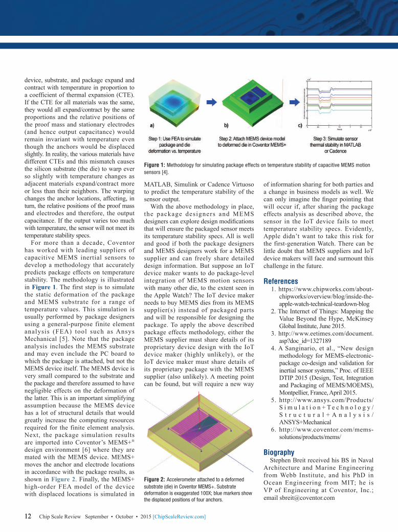
For more than a decade, Coventor has worked with leading suppliers of capacitive MEMS inertial sensors to develop a methodology that accurately predicts package effects on temperature stability. The methodology is illustrated in Figure 1. The first step is to simulate the static deformation of the package and MEMS substrate for a range of temperature values. This simulation is usually performed by package designers using a general-purpose finite element analysis (FEA) tool such as Ansys Mechanical [5]. Note that the package analysis includes the MEMS substrate and may even include the PC board to which the package is attached, but not the MEMS device itself. The MEMS device is very small compared to the substrate and the package and therefore assumed to have negligible effects on the deformation of the latter. This is an important simplifying assumption because the MEMS device has a lot of structural details that would greatly increase the computing resources required for the finite element analysis. Next, the package simulation results are imported into Coventor’s MEMS+® design environment [6] where they are mated with the MEMS device. MEMS+ moves the anchor and electrode locations in accordance with the package results, as shown in Figure 2. Finally, the MEMS+ high-order FEA model of the device with displaced locations is simulated in
MATLAB, Simulink or Cadence Virtuoso to predict the temperature stability of the sensor output.
With the above methodology in place, the package des igners and MEMS designers can explore design modifi cations that will ensure the packaged sensor meets its temperature stability specs. All is well and good if both the package designers and MEMS designers work for a MEMS supplier and can freely share detailed design information. But suppose an IoT device maker wants to do package-level integration of MEMS motion sensors with many other die, to the extent seen in the Apple Watch? The IoT device maker needs to buy MEMS dies from its MEMS supplier(s) instead of packaged parts and will be responsible for designing the package. To apply the above described package effects methodology, either the MEMS supplier must share details of its proprietary device design with the IoT device maker (highly unlikely), or the IoT device maker must share details of its proprietary package with the MEMS supplier (also unlikely). A meeting point can be found, but will require a new way
of information sharing for both parties and a change in business models as well. We can only imagine the fi nger pointing that will occur if, after sharing the package effects analysis as described above, the sensor in the IoT device fails to meet temperature stability specs. Evidently, Apple didn’t want to take this risk for the first-generation Watch. There can be little doubt that MEMS suppliers and IoT device makers will face and surmount this challenge in the future.
References1. https://www.chipworks.com/about-
chipworks/overview/blog/inside-the-apple-watch-technical-teardown-blog
2. The Internet of Things: Mapping the Value Beyond the Hype, McKinsey Global Institute, June 2015.
3. http://www.eetimes.com/document.asp?doc_id=1327189
4. A Sanginario, et al., “New design methodology for MEMS-electronic-package co-design and validation for inertial sensor systems,” Proc. of IEEE DTIP 2015 (Design, Test, Integration and Packaging of MEMS/MOEMS), Montpellier, France, April 2015.
5. http://www.ansys.com/Products/S i m u l a t i o n + T e c h n o l o g y /S t r u c t u r a l + A n a l y s i s /ANSYS+Mechanical
6. http://www.coventor.com/mems-solutions/products/mems/
BiographyStephen Breit received his BS in Naval
Architecture and Marine Engineering from Webb Institute, and his PhD in Ocean Engineering from MIT; he is VP of Engineering at Coventor, Inc.; email [email protected]
Figure 2: Accelerometer attached to a deformed substrate (die) in Coventor MEMS+. Substrate deformation is exaggerated 100X; blue markers show the displaced positions of four anchors.
Figure 1: Methodology for simulating package effects on temperature stability of capacitive MEMS motion sensors [4].

1515Chip Scale Review September • October • 2015 [ChipScaleReview.com]
Photonics integration and packaging gaining traction
By Hiren D. Thacker [Oracle] and Stefan Weiss [II-VI Laser Enterprise]
he ever-increasing demand for off-chip bandwidth in high-performance computing systems
is continuing to fuel the steady march of optical interconnects from outside-the-box transceiver components, to becoming an integral part of the silicon chipset. The integration and packaging of energy and bandwidth-efficient photonics components, active and passive, have requirements that are much different from those typical to logic and memory ICs. For example, hybrid integrated silicon photonic components require ultra-fine flip-chip interconnects for energy efficiency, single-mode optical interfaces (waveguide-to-waveguide or waveguide-to-fiber) require sub-micron alignment and placement accuracy, and PCBs may require embedded optical waveguides and couplers to facilitate optical ICs. Because these photonics-based communication highways will need to be intimately integrated with their electronic payload ICs, the worlds of photonics and electronic packaging must find a common footing. This trend was on display at the recently concluded IEEE Electronic Components and Technology Conference (ECTC) in San Diego, CA (May 27-30, 2015), where photonics integration and packaging dominated the optoelectronics packaging sessions. The well-attended sessions featured leading researchers in this fi eld from the USA, Europe and Asia, who presented their latest results in topics such as optical multi-chip modules (MCMs), semiconductor optical amplifier integration, optical I/Os, and more. In this article, we summarize these most recent results in the area of photonics/electronics integration and packaging presented at ECTC and expect that this will continue to be a hot-topic for the 2016 ECTC.
First session: focus on optical interconnects
The first session was entitled “Advanced Optical Interconnects.” The lead-off paper by Thacker, et al. was a joint publication from researchers at Oracle and Mellanox, wherein the authors described the packaging of a multi-chip wavelength division multiplexed (WDM) silicon photonics interconnect using
an all solid-state single-mode “photonic bridge” transport layer (Figure 1). The WDM link was built with hybrid integrated VLSI and Si photonics components and an off-chip laser; it was shown to successfully operate up to 10Gb/s while consuming <2pJ/bit on-chip power [1]. Following this, Ishigure, et al., of Keio University (Kyoto, Japan), winners of the Outstanding Session Paper at the 2014 ECTC, presented progress in their Mosquito method for fabricating single-mode polymer optical waveguides for board-level silicon photonics IC integration [2]. This unique method 3D prints waveguides, unlike the traditional lithography-based approach. The authors used a novel silicate-based organic/inorganic hybrid material for reducing optical loss and for improved thermal stability.
IBM Yorktown, IBM Bromont, and AFL Telecommunications, presented a joint paper on a manufacturing-capable approach for alignment and edge-coupled assembly of parallelized single-mode optical fi ber to silicon photonics ICs [3]. The current implementation, built using methods compatible with high-throughput pick-and-place tooling, can assemble one-dimensional fiber arrays of any size to a V-groove array on a silicon photonics chip. Using in-depth Monte Carlo analysis, they predict this method to yield an expected misalignment of less than 1.3μm between fiber-core and waveguide-coupler during manufacturing, which would be within the acceptable alignment range for single-mode photonics. The next presentation was focused on high-speed and compact optical
transceiver packaging. Researchers from Fujitsu Labs and Fujitsu Components described a double-sided mount card-edge-connected optical transceiver module (DCOM) that integrated an eight-channel optical transceiver using a high-speed FPC connector, inductive peaking line, and an integrated lens on the photodiode built using inkjet technology in a compact package [4]. The module was shown to be capable of 40Gb/s error-free transmission.
2.5D integration using glass and silicon interposers has been a hot topic in the packaging industry. Brusberg, along with his collaborators at Fraunhofer IZM, Contag AG, and TU Berlin, have been at the forefront of developing glass interposers with embedded optical interconnects. Their paper at the 2014 ECTC was winner of the Outstanding Interactive Session Paper Award. At the 2015 meeting, they demonstrated a multi-layer electro-optical circuit board (EOCB) with two embedded thin glass layers, planar integrated gradient-index multimode glass waveguides, a mid-board polymer-based out-of-plane coupling interface, and through-glass vias (TGVs) [5]. The TGVs were fabricated using a laser ablation process in combination with material plugging of the TGVs and mechanical drilling. From 2.5D integration to optoelectronic MCM packaging – the next paper by Tokunari et al., of IBM Japan – presented their work on the assembly and the demonstration of a high-bandwidth density optical MCM comprising bare VLSI and optical chips (VCSEL, photodetector)
T
Figure 1: Photo of a 5-chip, hybrid integrated energy-efficient WDM silicon photonics solid-state chip-to-chip interconnect subassembly. XNP2 and PUC are the hybrid bonded receiver and transmitter driver ICs, respectively [1]. Photo courtesy of Oracle.
GUEST EDITORIAL

1616 Chip Scale Review September • October • 2015 [ChipScaleReview.com]
mounted on an optical waveguide-laminated organic substrate [6]. The optical waveguide layer is manufactured via a dry fi lm lamination process, and laser-ablated mirrors formed on the waveguides couple light into and out of the optical chips and newly developed surface normal waveguide-fiber connectors. All channels of the demonstrator MCM package Tx and Rx operated up to 30Gb/s, achieving a bandwidth density of 15Gb/s/mm2, nearly eight times larger than that of optical fiber modules. In the final paper of the session, William Vis and his colleagues at the Georgia Tech Packaging Research Center in Atlanta reported on the design and proof-of-concept demonstration of 3D optical waveguides (3D WG) with 45 degree entry and exit planes with respect to optical through-glass vias [7]. They achieved this using a novel inclined lithography technique on an ultra-thin 3D glass substrate. Furthermore, the process enabled inherent alignment of the optical microstructure and the integration for chip-to-chip optical communication.
Second session: light sources for silicon photonics
The second session was entitled “Silicon Photonics and Light Sources.” The first paper was given by Budd et al., from IBM Yorktown Heights. They designed, fabricated, packaged and characterized a 4-channel semiconductor optical amplifier (SOA) flip-chip bonded to a photonics carrier with monolithically-integrated waveguide layers (Figures 2 and 3). Their fi rst samples showed good bond strength of the AuSn solder bumps and a net optical gain greater than 10dB [8]. The second paper by Schneider et al., was a joint publication from researchers of the Karlsruhe Institute of Technology, Germany and the National Sun Yat-sen University, Taiwan. They presented a blue LED module with an optical output power of 235.5W at an optical density of 111.6W/cm2. They achieved this by assembling 98 single LEDs with silver sintering onto an AlN substrate, which was cooled by a high-performance micro-channel water cooler. By using glass discs in front of the module doped with variations of phosphor concentration, they could adjust the color temperature [9]. Following this, Shubin et al., from Oracle showed results on a hybrid-assembled WDM photonics transceiver with 8 tunable channels operating at 10Gb/s per channel. The crucial
post-processing and packaging details to achieve the all solid-state photonics module were revealed [10]. La Porta, et al., from IBM Rüschlikon presented their fi rst results on the optical coupling of silicon photonics chips and polymer waveguides as a fi rst integration step for system-level assembly of silicon photonics building blocks operating at wavelengths of 1.3μm and 1.55μm. Using highly scalable adiabatic optical coupling, losses as low as 0.85dB for TE propagation at 1.3μm were achieved [11].
In the fifth paper, Uemura, et al., from PETRA, Japan, introduced an array of “optical pins” for a chip-scale parallel optical module. The optical pins are vertical waveguides made from UV-curable resin. A 125μm pitch x 12 channel optical pin array was successfully manufactured using a photolithographic method. This demonstrator showed low coupling losses of 0.41dB for the receiver and 2.3dB for the transmitter. A high coupling tolerance of >25μm at an allowable excess loss of 0.5dB have been achieved. The sixth paper given by Elger, et al., from the Technische Hochschule Ingolstadt, Germany, and Philips, Germany presented new designs for flip-chip bonded LEDs that are directly bonded onto PCB boards. Following the optical and electrical analyses, as well as thermal simulations of different designs,
prototypes have been assembled. The reliability was successfully tested for 1000 hours using thermal shock tests [13]. The final presentation by Wang, et al., from the Leibniz University in Hannover, Germany and the University of Freiburg, Germany, introduced a new packaging technology called “Optodic Bonding.” A low-power laser diode was successfully fl ip-chip bonded onto a flexible, transparent substrate using a UV adhesive. An additional lamination process strengthens the package [14].
Summary The ECTC Optoelectronics Packaging
subcommittee solicits papers on all topics pertaining to the design, development, and technology of packaging silicon photonics; optical interconnects; parallel optical transceivers; single mode or multicore connectors; optical waveguide coupling; optical chip-scale, heterogeneous, and microsystem integration; and 3D photonics; optoelectronic integration for the Internet of Things; high-efficiency LEDs and high-power lasers; and integrated optical sensors. Interested authors are encouraged to submit a 750-word abstract by October 12, 2015. Identify “Optolectronics” as your primary subcommittee. The 2016 ECTC will be held May 31–June 3, 2016 inLas Vegas, NV USA.
References1. H. Thacker, R. Shafiiha, J. Lexau, X.
Zheng, S. Djordjevic, S. Lin, et al., “Hybrid integration and packaging of an energy-efficient WDM silicon photonic chip-to-chip interconnect,” Proc. 65th ECTC 2015, May 26-29 San Diego, CA USA, pp. 762-767.
2. T. Ishigure, S. Yoshida, K. Yasuhara, D. Suganuma, “Low-loss single-mode polymer optical waveguide at 1550nm wavelength compatible with silicon photonics,” Proc. 65th ECTC 2015, May 26-29 San Diego, CA USA, pp. 768-774.
3. T. Barwicz, N. Boyer, S. Harel, T. Lichoulas, E. Kimbrell, A. Janta-Polczynski, et al., ” Automated, self-aligned assembly of 12 fibers per nanophotonic chip with standard microelectronics assembly tooling,” Proc. 65th ECTC 2015, May 26-29 San Diego, CA USA, pp. 775-782.
Figure 2: Photo of the semiconducting optical amplifier [8]. Photo courtesy of IBM.
Figure 3: Photo of the photonics carrier [8]. Photo courtesy of IBM.
1717Chip Scale Review September • October • 2015 [ChipScaleReview.com]
4. T. Yagisawa, T. Shiraishi, M. Sugawara, Y. Miki, T. Kondou, M. Kobayashi, et al., “40 Gb/s card-edge connected optical transceiver using novel high-speed connector,” Proc. 65th ECTC 2015, May 26-29 San Diego, CA USA, pp. 783-788.
5. L. Brusberg, H. Schröder, C. Ranzinger, M. Queisser, C. Herbst, S. Marx, et al.,“ Thin glass-based electro-optical circuit board (EOCB) with through-glass vias, gradient-index multimode optical waveguides and collimated beam mid-board coupling interfaces,” Proc. 65th ECTC 2015, May 26-29 San Diego, CA USA, pp. 789-798.
6. M. Tokunari, H. Hsu, S. Nakagawa, “Assembly and demonstration of high-bandwidth density optical MCM,” Proc. 65th ECTC 2015, May 26-29 San Diego, CA USA, pp. 799-803.
7. W. Vis, B. Chou, V. Sundaram, R. Tummala, “Self-aligned chip-to-chip optical interconnections in ultra-thin 3D glass interposers,” Proc. 65th ECTC 2015, May 26-29 San Diego, CA USA, pp. 804-809.
8. R. Budd, L. Schares, B. Lee, F. Doany, C. Baks, D. Kuchta, et al., “Semiconductor optical amplifier (SOA) packaging for scalable and gain-integrated silicon photonic switching platforms,” Proc. 65th ECTC 2015, May 26-29 San Diego, CA USA, pp. 1280-1286.
9. M. Schneider, B. Leyrer, B. Osswald, C. Herbold, F. Herrmann, K. Eilert, et al., “Blue and white light-emitting high-power density LED modules,” Proc. 65th ECTC 2015, May 26-29 San Diego, CA USA, pp. 1287-1292.
1 0 . I . S h u b i n , X . Z h e n g , H . T h a c k e r ,S. S. Djordjevic, S. Lin, P. Amberg, et al., “All solid-state multi-chip multi-channel WDM photonic module,” Proc. 65th ECTC 2015, May 26-29 San Diego, CA USA, pp. 1293-1298.
11. A. La Porta, J. Weiss, J. Dangel, D. Jubin, N. Meier, J. Hofrichter, et al., “Silicon photonics packaging for highly scalable optical interconnects,” Proc. 65th ECTC 2015, May 26-29 San Diego, CA USA, pp. 1299-1304.
12. T. Uemura, A. Ukita, K. Takemura, M. Kurihara, D. Okamoto, J. Ushida, et al., “125µm-pitch x 12-channel “optical pin” array as I/O structure for novel miniaturized optical transceiver chips,” Proc. 65th ECTC 2015, May 26-29 San Diego, CA USA, pp. 1305-1309.
13. G. Elger, M. Schmid, A. Hanß, E. Liu, M. Klein, U. Karbowski, et al., “Analysis of new direct on PCB board attached high-power fl ip-chip LEDs,” Proc. 65th ECTC 2015, May 26-29 San Diego, CA USA, pp. 1310-1317.
14. Y. Wang, R. Rother, L. Overmeyer, C. Müller, “Optoelectronic packaging on flexible substrates using flip-chip based optodic bonding,” Proc. 65th ECTC 2015, May 26-29 San Diego, CA USA, pp. 1318-1323.
BiographiesHiren D. Thacker received BS, MS, and PhD degrees in Electrical
and Computer Engineering from Georgia Tech. He is a Principal Packaging Engineer in the Photonic Products Group at Oracle; email: [email protected]
Stefan Weiss received his MSc in Physics from the U. of Hamburg, Germany. He is the Manager Back End Assembly at II-VI Laser Enterprise.

1818 Chip Scale Review September • October • 2015 [ChipScaleReview.com]
Packaging ICs to survive the automotive environment
By Prasad Dhond [Amkor Technology®]
lec t ronic sys tems in cars and trucks represent some of the harshest application conditions for integrated circuits
(ICs). The packaging for these ICs must withstand a variety of tests that go well beyond conditions prevalent in consumer, commercial and industrial qualifi cations.
To survive these tests and operate reliably over their expected lifetime in a variety of vehicles and systems, assembly processes for automotive ICs have several unique aspects to ensure packaging reliability and durability. The extent of unique processing and tests depends upon the vehicle system where the IC is employed.
G e t t i n g e l e c t r o n i c s i n t oproduct ion vehicles
Some electronics in vehicles are obvious, while others are somewhat hidden. The obvious systems include infotainment systems, digital displays, instrument cluster, voice/data communications, back-up warning, adaptive cruise control, advanced driver assistance systems (ADAS), cabin environmental controls, navigation systems, lane departure warning, and others in the passenger compartment.
The hidden vehicle systems include engine control, cylinder deactivation, electric power steering, electronic throttle control, airbag deployment, transmission control, anti-lock brakes, electronic stability systems, and more. Many of these hidden systems are mounted under the hood of the vehicle where the ambient temperature can be 150˚C or higher.
Vehicle electronics growth Over 50 different electronic systems can
be found in today’s high-end vehicles that implement the most advanced technologies. In fact, the number of automotive electronic systems is increasing due to government safety mandates and consumer demand for more convenience and comfort features.
In addition to the increasing electronic content, the number of vehicles sold is increasing globally, especially in China and emerging markets. In the last decade, new vehicle sales in China have grown at a rate of almost 12% per year.
Increasing vehicle sales a n d h i g h e r e l e c t r o n i c systems penetration are dr iv ing the automot ive I C m a r k e t , w h i c h i s a p p r o x i m a t e l y $ 2 4 B in 2015 , wi th a 5 -year CAGR o f abou t 9% to 10% (Figure 1). Over 70% of the automotive total available market (TAM) is in the area of analog (including linear regulators, power components, DC-DC converters, LED drivers and interface components, such as USB drivers) and microcontrollers (MCUs).
The automotive market is an attractive segment for most semiconductor companies as it provides a more stable application base compared to cyclical mobile or consumer applications, longer product life cycles, and higher returns on investment. However, there are barriers to entry with very high expectations of quality, reliability, handling and processing, all of which must be achieved at reasonable costs. There are also continuously evolving quality and reliability requirements that drive significant capital purchases. Working with the right outsourced semiconductor assembly and test (OSAT) partner can help address many of these challenges effectively.
AEC-Q100 gradesThe Automotive Electronics Council
(AEC) has established AEC-Q100, “Failure Mechanism Based Stress Test Qualification for Integrated Circuits” [1], to provide standardized test methodologies for reliable, high-quality electronic components.
Many of the tests in AEC-Q100 are performed by the IC suppliers themselves, but packaging-related tests may be performed by an OSAT as part of the IC qualification. The test requirements vary from “under-the-hood” applications, to passenger compartment, and other vehicle locations.
The part operating temperature grades are shown in Table 1.
The grades reflect different application profiles from under the hood to inside the cabin mounting locations and apply to IC products including microelectromechanical systems (MEMS) sensors, power devices, signal conditioning, MCUs and more. While Grade 1 is most commonly used in automotive, Grade 0 is for the more stringent applications, while Grades 2 and 3 are more equivalent to commercial qualifi cations.
S p e c i a l c o n s i d e r a t i o n s f o r automotive ICs
Semiconductor suppliers are not always aware that a particular IC will end up being used in an automotive application – especially if it’s a catalog IC being used in Grade 2 or Grade 3 applications such as after-market infotainment. If an IC is designed explicitly for an automotive application, however, steps must be taken to ensure that it is handled and processed differently than a standard
E
Figure 1: Market experts forecast consistent growth for automotive ICs. SOURCE: IC Insights.
Table 1: AEC-Q100 grades vary based on the operating environment temperature range.

1919Chip Scale Review September • October • 2015 [ChipScaleReview.com] 191919Chip Scale Review September September September • October • 2015 [ChipScaleReview.com]

2020 Chip Scale Review September • October • 2015 [ChipScaleReview.com]
40+ years of
WEB www.qinex.com
EMAIL [email protected]
CALL 1-508-236-1306
And now, the perfect nameQi•nex [kuh-nekts] 1. Over 40 years of reliable burn-in and custom connections; 2. Quality interconnects for nex-gen solutions.
TM
INNOVATION. More I/O choices, smaller form factors, superior performance in less time.
• Latest 3D design tools• On-site model shops• Rapid prototyping• Advanced thermal analysis• Design on demand• Broad range of innovative
contact designs
QUALITY. High-value interconnection solutions since 1970.
• 24/7 global engineering• 24/7 global support teams• Local engineering and sales• Six Sigma quality management• Proven, reliable high-volume
manufacturing• Expert molding, design, and
customization
PARTNERSHIP. In a fierce global market, only Qinex reliably supports the innovation, reputation and competitiveness of your business. We’ll work with you to get it right, the first time.
Introducing Qinex, the new brand name for superior interconnection solutions from Sensata Technologies. Qinex, the new word in perfect pitch.
40+ years of perfect pitch. And now, the perfect name.
commercial or industrial IC. Even a 1ppm component failure rate translates into a 1.5% or 15000ppm failure rate at the car level. To ensure the highest safety standards, we need to have a goal of zero defects.
When a product is identifi ed for automotive use, IC suppliers, especially those familiar with automotive requirements, usually have specific expectations for processing and handling during the assembly process.
Supplier managementEarly in the development process
of an automotive IC, one of the major considerations is business continuity planning with respect to raw materials. For instance, there have been major disruptions in the lead frame supply chain with recent accidents and some lead frame suppliers exiting the business. Supplier selection, redundancy, and process audits per automotive standards such as VDA6.3, are very important to ensure continuity and quality of supply for automotive ICs.
Automotive controlsIn addition to ensuring that factories
have automotive certifications such as TS16949, automotive products should be subject to tighter controls on the factory floor. Among other things, these controls might include designated automotive equipment (Figure 2), specially trained operators, error-proofing systems and hands-free processing systems. Designated automotive lines are usually equipped with higher end models of machines that are maintained at a different standard and subject to tighter Cpk process capability requirements. Certified operators are specially trained to handle automotive devices and have to meet certain minimum requirements to achieve and maintain certification. Process control automation can help ensure that automotive devices are processed only on designated automotive equipment by certifi ed operators.
Additional process stepsDepending on the application profile,
automotive devices could have additional process steps compared to a standard commercial IC to ensure the highest quality and reliability. These typically include more stringent visual inspections during assembly and 100% open-short testing at the end of the assembly process. Some of the other additional process steps could be direct plasma cleaning before wire bonding to ensure a higher quality bond and plasma cleaning before mold.
Safe launchSafe launch is a process during the pre-
production phase where manufacturers or assemblers inspect the process at each step and verify that the particular step is done correctly before the product moves to the next one. This ensures that any issues with production processes are identified and addressed during the pre-production phase itself, before high-volume production starts. Safe launch is even more important for advanced packages such as flip-chip ball grid array (FCBGA), flip-chip chip-scale package (fcCSP), system-in-package (SiP), etc., which are relatively new to automotive applications. For example, during the assembly process of FCBGA packages, safe launch could include examining cross sections at several different locations after the solder ball attach process to make sure that the metallurgy of the solder joints is robust. Although this represents extra work and time during pre-production runs, the benefi t is better quality and a more robust process. It also gives more confidence to both semiconductor suppliers and Tier 1 suppliers about going into production with new technologies.
AEC-Q100 qualification AEC-Q100 consists of a suite of tests but
only a subset of these tests is directly related to the package and assembly. Some of these are “in process” tests such as wire bond shear (WBS), wire bond pull (WBP), and others that an OSAT can perform. As shown in Figure 3, the reliability tests in test group A are the most applicable to an OSAT.
Traditional JEDEC and AEC-Q100 Test group A have various tests including pre-conditioning, temperature cycling (TC), temperature humidity bias (THB), unbiased highly accelerated stress test (HAST) and
high-temperature storage life (HTSL). Table 2 shows the differences between the standard JEDEC conditions vs. Grade 0 and Grade 1 automotive reliability test conditions. An OSAT must have reliability labs with capability and equipment to perform these tests.
Figure 4 shows the tests that Amkor t yp i ca l l y pe r fo rms fo r AEC-Q100 qualif icat ions. Based on equipment availability, or in some cases the equipment’s capability, alternate tests may be acceptable. For example, instead of unbiased HAST, autoclave or temperature humidity (without bias) are acceptable tests. These tests are used to characterize the bill of materials (BOM) for AEC-Q100 Grade 1 and Grade 0 applications. Different package families are evaluated to determine the most robust the most robust bill of materials (BOM) to qualify for Grade 0 and other grades.
Special BOM considerations In addition to special processing,
automotive applications frequently require special material sets or BOM. For lead frame products, some of the main material considerations are: wire type, epoxy mold compound (EMC), die attach (DA) materials, and lead frame design features.
Lead frames with roughened surfaces are often used to enhance EMC adhesion. Roughened lead frames can be used in combination with unique design features that are etched or stamped onto the lead frame surface to improve delamination performance.
A critical component in being able to achieve aggressive year-on-year cost reductions is to use copper wire on wire bond products. Traditionally, gold has been the wire of choice, but due to cost and high-temperature performance where Kirkendall voiding is observed between the gold and aluminum interface, most new wire bonded automotive devices are using copper wire. Most major
Figure 2: Typical wire bond assembly process steps and special identification label for designated automotive equipment.

40+ years of
WEB www.qinex.com
EMAIL [email protected]
CALL 1-508-236-1306
And now, the perfect nameQi•nex [kuh-nekts] 1. Over 40 years of reliable burn-in and custom connections; 2. Quality interconnects for nex-gen solutions.
TM
INNOVATION. More I/O choices, smaller form factors, superior performance in less time.
• Latest 3D design tools• On-site model shops• Rapid prototyping• Advanced thermal analysis• Design on demand• Broad range of innovative
contact designs
QUALITY. High-value interconnection solutions since 1970.
• 24/7 global engineering• 24/7 global support teams• Local engineering and sales• Six Sigma quality management• Proven, reliable high-volume
manufacturing• Expert molding, design, and
customization
PARTNERSHIP. In a fierce global market, only Qinex reliably supports the innovation, reputation and competitiveness of your business. We’ll work with you to get it right, the first time.
Introducing Qinex, the new brand name for superior interconnection solutions from Sensata Technologies. Qinex, the new word in perfect pitch.
40+ years of perfect pitch. And now, the perfect name.

2222 Chip Scale Review September • October • 2015 [ChipScaleReview.com]
IC suppliers are either already qualified, or are in the process of qualifying copper wire for automotive applications. Lead frame, chip-scale package (CSP) and ball grid array (BGA) packages are in volume production for infotainment and engine control applications, and there is also increasing acceptance in other applications such as powertrain and chassis. Safety applications, however, have been slower to adopt the use of copper wire.
The use of copper wire is not without its own set of challenges. Apart from the usual workability challenges of Cu wire, recent industry testing [2] has raised some concerns related to Pd coated copper (PCC) bond wire for very stringent automotive applications. In these studies, HTSL testing performed at above 150˚C showed degradation of bond
pull test (BPT) results seen over time, as well as cracks at the stitch bond area. While PCC wire passes the AEC-Q100 Grade 0 min levels, there are some concerns regarding the margin in very stringent applications where the IC must operate at temperatures over 150˚C for extended periods of time.
Further evaluations are necessary to validate the fi ndings of the above-mentioned study and determine the right material set to achieve robust performance for AEC-Q100 Grade 0 and beyond. Amkor has ongoing evaluations to determine appropriate BOMs for various products. The evaluation matrix for lead frame products consists of variations of wire type, EMC and lead frame design features. The primary goal of these evaluations is to develop a BOM recommendation for
AEC-Q100 Grade 0, with secondary goals of extended testing beyond the Grade 0 limits, to achieve zero delamination and meet other stringent automotive criteria.
Some of the Amkor package families that are popular in automotive electronic systems include: SOIC, TSSOP, MLF®/QFN, TQFP, BGA, Stacked CSP, fcCSP, FCBGA and TMV®. Dual lead frame products such as SOICs and TSSOPs represent the highest volume. Quad lead frame packages, as well as BGAs, are popular for automotive MCUs. The increasing use of non-wire bond products such as CSP and through-mold via (TMV®) is occurring in infotainment and ADAS systems.
Evolving automotive packaging requirements
Increasing innovation in ADAS and info ta inment i s b r ing ing advanced technologies to the automotive space at a much faster rate than ever before. Growing familiarity with smartphone technology is increasing consumer expectations in the car. Consumers now expect their car to seamlessly talk to their phones, and they want to be able to run the same apps that they are used to running on their phones, in their cars. New safety systems in the cars are slowly transitioning from driver assistance to highly automated, on their way to becoming autonomous. Autonomous operation requires automotive systems to continuously monitor the surroundings and take preventive actions in case an incident happens. In such a system, there are several sensors that feed real time data to a processor, where several algorithms are running and the processor feeds the results to actuators. Since these systems require real time processing, it is critical that the response time be as fast as possible. As a result, systems designers choose either SiP or fcCSP type of packaging to keep the processor and memory as close as possible to each other.
Assembly solutions for automotive IC packages
ICs provide the foundation for the technology inside the automotive electronic systems that deliver control features, convenience, connectivity and keep passengers safe and comfortable. To achieve the reliability that automakers demand, IC suppliers must approach IC packaging with considerably different packaging techniques. These include additional controls on the manufacturing floor, additional process steps during assembly, and using the right material set that has been proven to survive automotive reliability tests.
Figure 3: AEC-Q100 qualification test flow [1].
Table 2: AEC-Q100 qualification tests within an OSAT company’s scope.

2424 Chip Scale Review September • October • 2015 [ChipScaleReview.com]
EMULATIONTECHNOLOGY, INC
www.emulation.com1-800-232-7837
Fully automated or manually operated solutions to test any lead pitch & IC package
Quick TurnLow NRE
Custom Test Fixtures
Significantly reduce your socket & labor costs with these multiple
IC test and burn-in solutions.
Multi-Cavity Sockets
QuickOn/Off Lid
Easy Knobconfiguration
Easy Screw - Lid removed to show detail.
Lead pitches as low as 0.4mm, up to 125,000 insertions.Compression, SMT, &Thru-Hole PCB Mounting
As an OSAT suppl ie r wi th many y e a r s o f a u t o m o t i v e e x p e r i e n c e , Amkor Techno logy ® has ex tens ive understanding of the requirements of automotive OEMs and Tier 1 suppliers and can provide guidance and direction in assembling automotive products,
especially to customers with limited automotive experience. Our joint venture with J-Devices is expected to expand and provide even greater assembly and test capabili t ies for automotive customers, as well as access to the Japanese automotive market.
Evolving packaging technologies from leaded to surface mount to MEMS, 3D and die-level packaging will continue to place even more stringent demands on IC packages in automotive applications. Working with a seasoned expert OSAT can mean the difference between survival and failure in automotive applications.
References
1. AEC-Q100 Rev H, Failure Mechanism Based Stress Test Qualification for Integrated Circuits , http://www.aecouncil.com/Documents/AEC_Q100_Rev_H_Base_Document.pdf
2. Krinke JC et al. High temperature degradation of palladium coated copper bond wires. Microelectron Reliab (2014), http://dx.doi.org/10.1016/j.microrel.2014.07.097
BiographyPrasad Dhond received his BSEE
from The U. of Texas at Austin, and MBA from Southern Methodist U. and is Sr. Director Dual & Quad Leadframe P r o d u c t s a t A m k o r Te c h n o l o g y ®; email [email protected]
Figure 4: AEC-Q100 Group A tests performed by Amkor Technology®.
2525Chip Scale Review September • October • 2015 [ChipScaleReview.com]
Out of this world electronics packaging
By Andrew A. Shapiro [Jet Propulsion Laboratory, California Institute of Technology]
l e c t r o n i c s p a c k a g i n g f o r space exploration challenges conventional strategies and materials. Venus exploration will
encounter extreme high temperatures and pressures with a highly corrosive atmosphere. There is a vast array of environments for operations on frozen worlds, some with no atmosphere, such as Europa, or others, such as Titan, with a cold methane atmosphere and methane lakes. The surface of Mars can have extreme cycles daily.Deep space measurements of the origin of the universe can require electronics measuring less than 1mK. Traditional strategies have often used warm electronics boxes to minimize electronics temperature excursions, however, with the growth of small spacecraft and of nano- or micro-robotic systems, the power budgets for many future NASA mission concepts cannot support warming of the spacecraft electronics. Additionally, surface exploration of icy ocean worlds, such as Enceladus or Ganymede, where power availability may be extremely limited, electronics need to be designed and packaged to operate at or near these extremes.
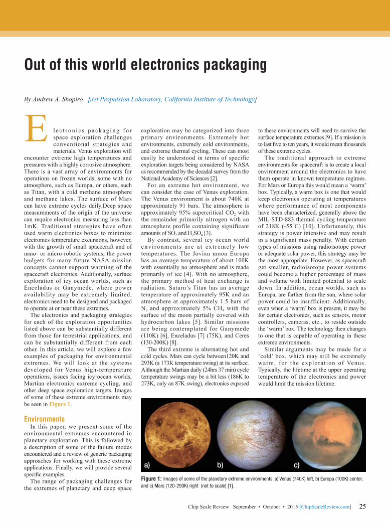
The electronics and packaging strategies for each of the exploration opportunities listed above can be substantially different from those for terrestrial applications, and can be substantially different from each other. In this article, we will explore a few examples of packaging for environmental extremes. We will look at the systems developed for Venus high-temperature operations, issues facing icy ocean worlds, Martian electronics extreme cycling, and other deep space exploration targets. Images of some of these extreme environments may be seen in Figure 1.
EnvironmentsIn this paper, we present some of the
environmental extremes encountered in planetary exploration. This is followed by a description of some of the failure modes encountered and a review of generic packaging approaches for working with these extreme applications. Finally, we will provide several specifi c examples.
The range of packaging challenges for the extremes of planetary and deep space
exploration may be categorized into three primary environments. Extremely hot environments, extremely cold environments, and extreme thermal cycling. These can most easily be understood in terms of specific exploration targets being considered by NASA as recommended by the decadal survey from the National Academy of Sciences [2].
For an extreme hot environment, we can consider the case of Venus exploration. The Venus environment is about 740K at approximately 91 bars. The atmosphere is approximately 95% supercritical CO2 with the remainder primarily nitrogen with an atmosphere profile containing significant amounts of SO2 and H2SO4 [3].
By contrast, several icy ocean world env i ronments a re a t ex t remely low temperatures. The Jovian moon Europa has an average temperature of about 100K with essentially no atmosphere and is made primarily of ice [4]. With no atmosphere, the primary method of heat exchange is radiation. Saturn’s Titan has an average temperature of approximately 95K and an atmosphere at approximately 1.5 bars of N2 and approximately 5% CH4 with the surface of the moon partially covered with hydrocarbon lakes [5]. Similar missions are being contemplated for Ganymede (110K) [6], Enceladus [7] (75K), and Ceres (130-200K) [8].
The third extreme is alternating hot and cold cycles. Mars can cycle between120K and 293K (a 173K temperature swing) at its surface. Although the Martian daily (24hrs 37 min) cycle temperature swings may be a bit less (186K to 273K, only an 87K swing), electronics exposed
to these environments will need to survive the surface temperature extremes [9]. If a mission is to last fi ve to ten years, it would mean thousands of these extreme cycles.
The traditional approach to extreme environments for spacecraft is to create a local environment around the electronics to have them operate in known temperature regimes. For Mars or Europa this would mean a ‘warm’ box. Typically, a warm box is one that would keep electronics operating at temperatures where performance of most components have been characterized, generally above the MIL-STD-883 thermal cycling temperature of 218K (-55˚C) [10]. Unfortunately, this strategy is power intensive and may result in a significant mass penalty. With certain types of missions using radioisotope power or adequate solar power, this strategy may be the most appropriate. However, as spacecraft get smaller, radioisotope power systems could become a higher percentage of mass and volume with limited potential to scale down. In addition, ocean worlds, such as Europa, are farther from the sun, where solar power could be insufficient. Additionally, even when a ‘warm’ box is present, it may be for certain electronics, such as sensors, motor controllers, cameras, etc., to reside outside the ‘warm’ box. The technology then changes to one that is capable of operating in these extreme environments.
Similar arguments may be made for a ‘cold’ box, which may still be extremely warm, for the explorat ion of Venus. Typically, the lifetime at the upper operating temperature of the electronics and power would limit the mission lifetime.
E
Figure 1: Images of some of the planetary extreme environments: a) Venus (740K) left, b) Europa (100K) center, and c) Mars (120-293K) right (not to scale) [1].

2626 Chip Scale Review September • October • 2015 [ChipScaleReview.com]
standard Si semiconductors cannot function at this temperature. The solution involved not only a new integrated circuit approach using SiC, but a new packaging scheme was needed. Packaging traditionally depends on widespread use of polymers for things like die attach, printed wiring boards, solder masks and conformal coatings. Most of these burn or melt well below the 740K environment of Venus. Traditional solders will also melt well below this temperature. Thick-film circuit interconnects were used with high-temperature solders for demonstration of a combined multiplexer-amplifi er circuit that operates at 773K (shown in Figure 3) [14]. Alternative approaches included miniaturized vacuum tubes, which have high survivability because of their larger feature size.
Icy ocean worlds. Another extreme environment example is the extreme cold of icy ocean worlds such as Titan or Europa. The ice formations on Europa at 90K may be seen in Figure 5. There is speculation that a water ocean exists 10km below the surface ice [6]. In order to perform sample measurements, or to have external cameras, some of the electronics would need to be in the ambient environment. The traditional heating of electronics is limited because the solar radiation is too small to make use of photovoltaic cells, and batteries do not perform well in these extreme cold environments. At cold temperatures, there are some issues with CMOS semiconductors including excessive hot carriers and possible device degradation, however, with clever device design, the effects can be mitigated using SiGe technology [15]. Additional issues in the interconnect with traditional Sn-based solders also must be addressed. Careful study reveals that alloying with In nearly eliminates
Figure 3: A multiplexer designed for and successfully operated in a simulated Venus environment [14].
Failure modesIn consideration of the performance of the
electronics at these extreme temperatures, we have to parse the assemblies into different technologies and assess them. One way to parse the system is into: active devices; passive devices, interconnects, and assembly materials.
Active devices, for example, can include integrated circuits in silicon, III-IV and II-VI devices. Performance at cold temperatures can be substantially different. Clocks can run at different speeds, carriers can freeze out, and mobilities can be substantially different. Space or planetary radiation may have effects on the performance of some devices. At high temperatures, lifetimes of devices can become an issue. Wider band gap materials, such as SiC or CDia, may function more effectively.
Passive devices, including integrated passives, can also have substantial changes in performance. The polarization mechanisms used to store charge in capacitors may not be active, thermal coefficients of capacitance (TCCs), and thermal coeffi cients of resistance (TCRs), can become nonlinear, and in many cases are unknown at the extreme hot or cold temperatures. Magnetic properties for inductor and transformer materials can go below the Curie temperature, or can be excessively noisy at higher temperatures.
Interconnects can also be challenging. In cold environments, Sn-based solders can have issues because Sn undergoes two transitions at cold temperatures. It undergoes an allotropic phase transition at 286.2K—undergoing a Snb→Sna transformation. This transformation includes a 27% volume increase, so in addition to having a new structure, the mechanical integrity is disrupted by catastrophic rupture. This transformation is known to have very slow kinetics, so the transition may occur years after being exposed to temperatures below the transition. Interestingly, Cu can accelerate the transition to occur in just a few hours. With Cu being present in most interconnect systems containing Sn-based solders, the presence of Cu could become a serious issue even with Ni barrier layers [11].
Additionally, if the transition described above is avoided, Sn, and many Sn alloys, will also undergo a ductile to brittle transition (DTBT) at about 150K [12]. This DTBT substantially lowers the mechanical integrity of the Sn and would be likely to cause catastrophic failure of the electronics assemblies if standard techniques are used.
Other common failure modes found in standard electronics assemblies involved cyclic fatigue of Au wire bonds, Sn-based solder joints, and Cu vias in polyimide printed wiring boards. Polymers can fail through brittle fracture in cold environments. In hot environments, thermoplastic polymers soften and in thermoset polymers sublimation, or even burning can be an issue. In both cold and hot environments,
polymers suffer from adhesion loss. Hot environments, can also offer challenges for metals. Diffusion and electromigration are accelerated. Most traditional solders will melt well below the Venus ambient temperature, and many other metal interconnects suffer from changes in properties or crystal structure because of diffusion or creep, which are accelerated at higher temperatures [13].
ApproachThe general strategy for electronics in
extreme environmental conditions is to first determine which items need to be maintained inside the spacecraft, and which items need to be exposed to and can operate in the extreme environments. With the current emphasis on smaller, cheaper missions, this balance is changing with more of the electronics being exposed to the extreme environments as the power and mass required to maintain a more benign environment is not available.
The process for evaluation may be thought of in the following sequence: 1) First, review power and mass budgets, select components and interconnects requiring extreme exposure; 2) Next, review the list of materials and components requiring exposure for compatibility with the environment to determine which ones can perform suitably in the environment and which ones require further study; 3) At this point, many of the materials systems for interconnects cannot perform as needed and new materials sets need to be developed taking into consideration minimization of stress and maximizing component and system performance. Also, performance data and even physics-based models of materials and components are often not available at the extremes such as 90K or 740K. New materials sets need to be selected with regard to fundamental physics, and then the selections need to be validated to obtain and to verify cold/hot performance data both individually, and as a system. A few examples are provided in the next section.
Materials selection for extreme environments
T h r e e e x a m p l e s a r e r e v i e w e d f o r h o w m a t e r i a l s s y s t e m s w e r e evaluated for selection to perform in extreme environments.
Ve n u s e l e c t r o n i c s . T h e Ve n u s environment creates a completely different set of challenges from those faced by most packaging engineers. An image of the Venus environment may be seen in Figure 2. The focus of the packaging for Venus surface mission concepts was to construct a small-scale electronic sensing system and transmitter that could function in the 740K, 91 bar ambient. This solution took somewhat more creativity because the
Figure 2: The Venus environment (740K) [1].
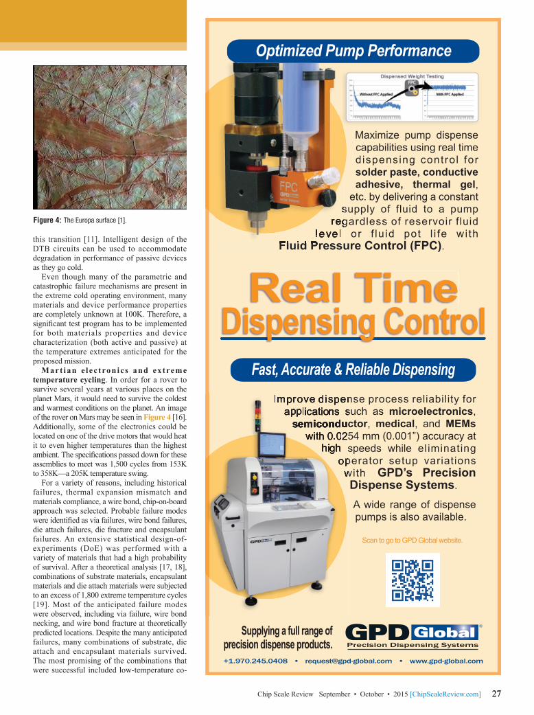
2727Chip Scale Review September • October • 2015 [ChipScaleReview.com]
this transition [11]. Intelligent design of the DTB circuits can be used to accommodate degradation in performance of passive devices as they go cold.
Even though many of the parametric and catastrophic failure mechanisms are present in the extreme cold operating environment, many materials and device performance properties are completely unknown at 100K. Therefore, a signifi cant test program has to be implemented for both materials properties and device characterization (both active and passive) at the temperature extremes anticipated for the proposed mission.
Mart ian e l ec tron ics and ex treme temperature cycling. In order for a rover to survive several years at various places on the planet Mars, it would need to survive the coldest and warmest conditions on the planet. An image of the rover on Mars may be seen in Figure 4 [16]. Additionally, some of the electronics could be located on one of the drive motors that would heat it to even higher temperatures than the highest ambient. The specifi cations passed down for these assemblies to meet was 1,500 cycles from 153K to 358K—a 205K temperature swing.
For a variety of reasons, including historical failures, thermal expansion mismatch and materials compliance, a wire bond, chip-on-board approach was selected. Probable failure modes were identifi ed as via failures, wire bond failures, die attach failures, die fracture and encapsulant failures. An extensive statistical design-of-experiments (DoE) was performed with a variety of materials that had a high probability of survival. After a theoretical analysis [17, 18], combinations of substrate materials, encapsulant materials and die attach materials were subjected to an excess of 1,800 extreme temperature cycles [19]. Most of the anticipated failure modes were observed, including via failure, wire bond necking, and wire bond fracture at theoretically predicted locations. Despite the many anticipated failures, many combinations of substrate, die attach and encapsulant materials survived. The most promising of the combinations that were successful included low-temperature co-
Figure 4: The Europa surface [1].

2828 Chip Scale Review September • October • 2015 [ChipScaleReview.com]
AcknowledgementsPar t o f th i s r e sea rch was ca r r i ed
out at the Jet Propulsion Laboratory,California Institute of Technology, under a contract with the National Aeronautics and Space Administration.
References1 . S t a f f , “ P h o t o j o u r n a l , ” h t t p : / /
p h o t o j o u r n a l . j p l . n a s a . g o v / , J e t P r o p u l s i o n L a b o r a t o r y , Retrieved 7/30/15.
2. “Visions and Voyages for Planetary Science in the Decade 2013-2022: a report of the National Research Council,” Committee on the Planetary Science Decadal Survey, Space Studies Board Division on Engineering and Physical Sciences, National Research Council of the National Academies, March 2011.
3. V. A. Krasnopolsky, V. A. Parshev, “Chemica l compos i t i on o f t he atmosphere of Venus,” Nature,Vol. 292, Issue: 5824, pp. 610-613, 13 Aug. 1981; doi:10.1038/292610a0.
4. R. T. Pappalardo, W. B. McKinnon, K. Khurana, “Atmosphere of Europa,” Europa, U. of Arizona Press, 2009; ISBN 0-8165-2844-6.
fired ceramic (LTCC) substrates, epoxy die-attach and Parylene encapsulant, although Al2O3 and polyimide substrates also worked
with certain combinations. Assemblies with these combinations were tested through more than 1,800 extreme temperature cycles while continuously operating, demonstrating excellent performance for an extended Mars mission with the packaged electronics exposed to the extreme ambient. Figure 6 shows an example of an assembly for a motor driver designed for Mars rovers that survives these extreme cycles [20].
SummaryThe task of packaging electronics for
planetary exploration can experience challenges far beyond those typically encountered in commercial electronics. Understanding the fundamental materials properties and physics-of-failure are absolute necessities for mission success. This understanding is needed to inform the design, build, test and verification of electronics sub-systems. Because most of the materials properties and performance of devices are not well known in many of these extreme environments, significant testing at the environmental extremes needs to be performed in order to obtain the required knowledge to support the design of extreme-survivable electronics systems.
R&D Altanova 3601 So. Clinton Ave. South Plainfield, NJ 07080
rdaltanova.com
CONTACT US | [email protected]
5.309 mil
1.012 mil
High Aspect Ratio LoadBoard Drilling & Plating
• 0.4mm pitch
• 4.75mm thick
• 37:1 Aspect Ratio
• 1 mil plating
CONQUER COMPLEXITY
RDA_Ad_CSR_Apr14_M.indd 1 4/8/14 1:00 PM
Figure 5: The Mars Science Lander (artist’s concept) [16].
Figure 6: Chip-on-board motor driver assembly developed for the extreme temperature cycling of Mars [20].

2929Chip Scale Review September • October • 2015 [ChipScaleReview.com]
5. G. Mitri, A. P. Showman, J. I. Lunine, R. D. Lorenz, "Hydrocarbon lakes on Titan," Icarus, Vol. 186 Issue: 2, pp. 385–394, 2007. Bibcode:2007Icar..186..385M. doi:10.1016/j.icarus.2006.09.004.
6. M. L. Delitsky, A. L. Lane, “Ice chemistry on the Galilean satellites,” Jour. of Geophysical Research: Planets, Vol. 103, Issue: E13, pp. 31391-31403, 25 Dec. 1998.
7. C. C. Porco, P. Helfenstein, P. C. Thomas, A. P. Ingersoll, J. Wisdom, R. West, et al., (10 Mar. 2006); "Cassini observes the active South Pole of Enceladus," Science 311 (5766): 1393–1401.
8. J. A. Angelo, Jr., Encyclopedia of Space and Astronomy. New York: Infobase, p. 122, 2006. ISBN 0-8160-5330-8
9. Staff, “Mars Facts,” NASA. Retrieved July 13, 2015 http://mars.nasa.gov/allaboutmars/facts/.
10. MIL-STD-883 – Test method for microcircuits, Rev. J w/Change 5, Method 1010; 1 June, 2015.
11. A. Lupinacci, A. A. Shapiro, J. O. Suh, A. M. Minor, “A study of solder alloy ductility for cryogenic applications,” 15th IEEE Inter. Symp. and Exhibition on Advanced Packaging Materials, Irvine, CA, Feb. 27–Mar. 1, 2013.
12. A. Lupinacci, J. Kacher, A. Eilenber, A. A. Shapiro, P. Hosemann, A.M. Minor, “Cryogenic in situ micro-compression testing of Sn, Acta Materialia, Vol. 78 pp. 56-64, 1 Oct. 2014.
13. L. Del Castillo, “Failure analysis of electronic packaging,” from Part X Packaging for Extreme Environments, Ch. 68 , “Ext reme Environment Electronics,” J. D. Cressler, H. A. Mantooth, Eds., Nov. 26, 2012, pp.791-800, CRC Press, ISBN 9781439874301.
14. L. Del Castillo, “Extreme-temperature sensing system for the Venus ambient environment,” JPL Internal Report R.06.023.005, Oct. 2007.
15. T. Chen, C. Zhu, N. Najafi zadeh, B. Jun, A. Ahmed, R. Diestelhorst, et al., “CMOS reliability issues for emerging cryogenic lunar electronics applications,” Solid-State Electr., Vol. 50, pp. 959–963, 2006.
16. “Mars Science Laboratory,” http://m a r s m o b i l e . j p l . n a s a . g o v /multimedia/images/?ImageID=2098, J e t P r o p u l s i o n L a b o r a t o r y ,Retrieved 7/30/15.
17. K. K. Jinka, S. Ganesan, A. Dasgupta, S. Ling, A. A. Shapiro, D. Schatzel, “Chip-on-board (CoB) technology for low-temperature environments, Part I: Wire profile modeling in unencapsulated chips,” Microelectron. Reliabil., Vol. 47, pp. 1246–1250, 2007.
18. K. K. Jinka, A. Dasgupta, S. Ganesan, S. Ling, “Chip-on board technology
for low-temperature environment. Part II: Thermomechanical stresses in encapsulated ball-wedge bond wires,” Microelectron. Reliabil., Vol. 49, pp. 523–529, 2009.
19. A. A. Shapiro, C. Tudryn, D. Schatzel, S. Tseng, “Electronic packaging m a t e r i a l s f o r e x t r e m e , l o w -temperature, fatigue environments,” IEEE Trans. on Adv. Pkg. Vol. 23, No. 2, pp. 408-420, May 2010.
20. D. Hunter, personal communication, NASA Jet Propulsion Laboratory, July, 2015.
BiographyAndrew A. Shapiro received his PhD in
Materials Science from the U. of California, Irvine and is the Manager for Early Stage Innovation in the Space Technology Office at the Jet Propulsion Laboratory, Ca l i fo rn ia Ins t i tu te o f Technology; email [email protected]
DL Technology216 River Street, Haverhill, MA 01832P: 978.374.6451 | F: 978.372.4889 [email protected]
Our Point Is... DL Technology Needles Work Precisely For Any Application.DL Technology needles are designed and crafted to dispense material accurately, ef�ciently and to provide for better material release. Our needles are constructed in a variety of sizes, con�gurations, and patterns to meet your needs for any application.
EZ-FLO needles available in footed and non-footed surface mount, encapsulation, luer, and cone. Designed to provide precise, repeatable volumes. Stainless steel and ceramic needles available.
Easy Release Luer-lok dispense needles available in stainless steel and plastic. Used for applications such as epoxy, solder paste, solder mask and a variety of other materials.
Custom Needles can be designed according to unique requirements and speci�cations.
DL Technology has been the leader in micro dispensing technology for over 15 years. For more information, or for size or speci�cations on our line of needles, pumps or valves, visit www.dltechnology.com.
to provide precise, repeatable volumes. Stainless steel
DL Technology Needles Work Precisely For Any
DL Technology needles are designed and crafted to dispense material accurately, ef�ciently and to provide for better material

3030 Chip Scale Review September • October • 2015 [ChipScaleReview.com]
Thermocompression bonding for flip-chip technology
By John H. Lau, Li Ming, Nelson Fan, Ringo Tse [ASM Pacifi c Technology Ltd.]
l ip -ch ip t echno logy has been used ex tens ive ly for the processors of mainframe
computers, servers, personal computers, notebooks, smartphones, tablets, games, etc., the application-specific integrated c i r c u i t s ( A S I C s ) o f n e t w o r k i n g , t e l ecommunica t ions , e t c . , and the memories of data storage devices, etc. Recently, because of the requirements of higher functionalities of the chips and shrinking the chips’ area, the number of pin-outs of the processors, ASICs, and memories increases and their pitch (or the spacing between the pin-out pads) decreases. Also, because of the trends of smaller form factors for mobile (e.g., smartphones and tablets) and portable (e.g., notebooks) products, the thickness of the chips and package substrates must be as thin as possible. Higher pin counts, tighter pitches, thinner chips, and lower profile package substrates lead to the necessity of the thermocompression bonding (TCB) method for flip-chip assemblies. In this study, various TCB techniques are investigated and a new process is proposed.
Wafer bumpingFlip-chip technology was introduced
by IBM in the 1960s [1, 2], and solder bumps are its most important element. There are many ways to perform the wafer bumping (at least 12 are shown in [3]), and the most common method is by electroplating (as shown in Figure 1).
C4 bumpsUsually the pad size is equal to 100μm
and the target bump height is equal to 100μm. After redefining the passivation opening (usually it is not required), either Ti or TiW (0.1 to 0.2μm) are sputtered over the entire surface of the wafer fi rst, followed by 0.3 to 0.8μm of Cu. Ti-Cu and TiW-Cu are called under bump metallurgy (UBM). In order to obtain 100μm bump height, a 40μm layer of resist is then overlaid on the Ti-
Cu or TiW-Cu and a solder bump mask is used to define (UV exposure) the bump pattern as shown in steps #1-4 in Figure 1. The opening in t he r e s i s t i s 7 t o 10μm wider than the pad opening in the passivation layer. A 5μm layer of Cu is then plated over the UBM, followed by electroplat ing the solder. This is done by applying a static or pulsed current through the plating bath with the wafer as the cathode. In order to plate enough solder to achieve the target (100μm), the solder is plated over the resist coating by about 15μm to form a mushroom shape. The resist is then stripped off and the Ti-Cu or TiW-Cu is removed with a hydrogen peroxide or plasma etching. The wafer is then reflowed with flux, which creates smooth truncated spherical solder C4 (controlled collapsed chip connection) bumps due to surface tension as shown in steps #5 through #8 on the left-hand side of Figure 1.
C2 (Cu-pillar with solder cap) bumps
Because of higher pin-count and tighter pitch (very small spacing between pads), there is a possibility of shorting the adjacent solder C4 bumps. Wire interconnects [4] and Cu-pillar with solder cap [5-7] as shown on the right-hand side of Figure 1 can be a solution. The fabrication process is basically the same as that of the C4 bumps except electroplating the Cu instead of solder as shown in step #5 on the right-hand side of Figure 1. It is followed by electroplating the solder cap
and then reflowing the solder with flux. Because the solder volume is very small compared with the C4 bump, the surface tension is not enough to perform the self-alignment of the Cu pillar with the solder cap bump and therefore, it is sometimes called a C2 (chip connection) bump.
Flip-chip assemblyFigure 2 shows some methods of
f l ip-chip assembly and their range (spacing between pads/pillars/bumps) of applications. Basically, there are two groups: one is with an intermediate layer between the bonding pads/traces, and the other is not, i.e., nothing! Flip-chip assembly with intermediate layers such as solder mass reflow and solder by TCB are called indirect bonding. Cu-to-Cu diffusion bonding, which does not have anything between the bonding pads/traces on the chip/wafer is, therefore, called direct bonding.
Cu-to-Cu TCB direct bondingCu-to-Cu diffusion bonding can go
down to ultra-fine pitch and pad size (the spacing between pads is 5µm or
F
Figure 1: Electroplating wafer bumping process for a) C4 bumps (left) and b) C2 (Cu-pillar with solder cap) bumps (right).

3131Chip Scale Review September • October • 2015 [ChipScaleReview.com]
less); sometimes it is even used for larger spacing between pads at 20µm. In order to reduce the tendency to form native oxides that strongly affect the bonding reliability, Cu-to-Cu is a TCB and usually operates at high temperature (~400˚C) and pressure and long process time (60-120 minutes), which are not good for throughput and the device reliability. On the other hand, Cu-to-Cu bonding at room temperature leads to the highest throughput and the least amount of device reliability concerns, as well as very low costs. However, the drawbacks of room temperature bonding are the stringent requirements on: 1) pad/trace/wafer planarization, 2) surface treatment to ensure smooth hydrophilic surfaces for high quality bonding, and 3) the class of clean room is very high. Cu-to-Cu TCB is mainly for wafer-to-wafer (W2W), chip-to-wafer (C2W), and chip-to-chip (C2C) assembly processes.
C4 solder reflowSolder mass reflow has been using for flip-chip assembly for
almost 50 years. Most of the solder C4 bumps are mass refl owed on either silicon, ceramic or organic substrates. The assembly process is very simple: 1) Use a look-up and look-down camera to identify the location of the bumps on the chip and the pads on the substrate; 2) Apply fl ux on either the C4 bumps, or the substrate, or both; 3) Pick and place the C4 bumped chips on the substrate, then mass refl ow. Because of the surface tension of the C4 solder bumps during refl ow, the process is very robust (self-alignment). The spacing between the bumps on the solder mass refl ow of C4 bumped chips can be as small as 50µm as shown in Figure 2.
C2 solder reflowIn the past few years, solder mass reflow of C2 (Cu-pillar with
solder cap) bumped chips on either silicon, ceramic or organic package substrates has been very popular for high pin-count and fi ne-pitch fl ip-chip assembly. The assembly process is exactly the same as that of the C4 bumps, but the self-alignment characteristic is nowhere near the same. The spacing between the pillars on the solder mass refl ow of C2 bumped chips can be as small as 25µm as shown in Figure 2.
ASM’s high productivity (9,000 UPH) with individual dual fl ip-chip bonding system AD9212 [8] is specifi cally designed for solder mass refl ow of C4 and C2 bumped chips. The placement accuracy in the xy-direction is ±5µm @ 3σ and die rotation is ±0.03˚ @ 3σ. The wafer
Figure 2: Various flip-chip assembly processes vs. spacing between pads/pillars/bumps.
©2015 Indium Corporation
ASIA • CHINA • EUROPE • USA
www.indium.com [email protected]
Learn more:http://indium.us/E042
See us at: • IMAPS Booth 517• Productronica
Hall A4 Booth 214
Eliminates the cost of cleaning away flux residues. Prevents damage to both die and joints caused by cleaning processes.• Flip-Chip Flux NC-26-A
– Used in multiple mobile flip-chip packages
• Flip-Chip Flux NC-26S – Suited for large area, fine pitch (≤60micron) die
• Flip-Chip Flux NC-699 – Lowest residue of any flux in use in flip-chip production (near-zero residue)
Ultra-Low Residue No-Clean Flip-Chip Fluxes

3232 Chip Scale Review September • October • 2015 [ChipScaleReview.com]
attracting attentions for high-density and ultra-fine pitch flip-chip assembly. Basically, there are two methods, one is with low bonding force and the other is with high bonding force. For the one with low bonding force, the assembly process is simple: 1) First, use the look-up and look-down camera to locate the position of the C2 bumps on the chip and their corresponding pads on the substrate; 2) Apply flux on the solder cap or on the substrate or both; 3) Pick-and-place the chip o n t h e s u b s t r a t e a n d t h e n a p p l y temperature to melt the solder and a low force to hold the chip at a certain distance from the substrate. The above procedure is done one chip at a time and therefore, the throughput is low in compar ison wi th the C2 solder mass ref low process . The spacing between the pillars on the C2 chip by TCB with a low bonding force can be as small as 8µm.
ASM specifically designed a TCB bonder wi th a low bond ing fo rce for use with C2 bumped chips on a package substrate; it has been used for high-volume manufacturing by Intel [9] for thin chips and thin substrates. The process is very simple. First, the thin substrate is pre-applied flux and held flat on the hot pedestal under v a c u u m . T h e t h i n c h i p i s p i c k e d up by the bond head, held securely flat, with vacuum. After the chip is aligned with the substrate, the bond head comes down and stops when the Cu pillar of the chip touches the pad of the substrate. A constant force is then applied while the chip is quickly heated beyond the solidus temperature. As soon as the solder melts, the chip i s moved fu r the r down to ensu re good contact. After a certain bonding time, the heater and the solder joints are cooled rapidly below the solidus temperature. The inert environment is less than 100ppm oxygen around the bond head and nozzle, thereby pro tec t ing the Cu f rom ox ida t ion during heat up. The process time is 4 seconds and below, so the UPH (units per hour) is 900 or more [9].
F o r T C B w i t h a h i g h - b o n d i n g force on the C2 chip, the assembly p r o c e s s m u s t b e c o m b i n e d w i t h the nonconduct ive paste (NCP) or film (NCF) underfill, which will be discussed in the next section.
C2 TCB indirect bondingI n t h e p a s t f e w y e a r s , T C B o f
ch ip s w i th an i n t e rmed ia t e l aye r such as C2 (Cu-pi l lar wi th solder cap) bumps on si l icon, ceramic or organic package substrates, has been
handling capability is up to 300mm and the chip size range is up to 30mm x 30mm. It supports a flux dipping flip-chip process and is convertible between fl ip-chip and die attach processes.
Figure 4: Cross-section image of Qualcomm’s SNAPDRAGON 805 processor manufactured using high-force TCB of a C2 bumped chip on substrate with NCP.
Figure 3: Stencil printing of underfill for flip chips on an organic-panel assembly: a) Before printing; b) During printing; c) After printing; and d) After capillary action (hot air optional).

3333Chip Scale Review September • October • 2015 [ChipScaleReview.com]
UnderfillsIn 1987, Hitachi showed that with
underfill, the thermal fatigue life of the flip-chip solder joints on ceramic substrate increased [10]. Five years l a t e r , I B M a t Ya s u p r o p o s e d t h e use of a low-cost organic substrate i n s t e a d o f t h e h i g h - c o s t c e r a m i c subs t ra te for f l ip-chip assembl ies [11]. They showed that with underfill, the large thermal expansion mismatch between the sil icon chip (2.5x10⁻⁶/oC) and the organic substrate (15-18x10-6/oC) is reduced substantially, and the solder joints are reliable for most applicat ions. This opened up the doors for today’s very popular so lde r bumped f l i p - ch ip on l ow-c o s t o rg a n i c s u b s t r a t e p a c k a g e s used, for example, in the processors of personal computers, notebooks, smartphones, tablets, etc. Basically, there are two different procedures to apply the underfill , namely pre-assembly underfill, and post-assembly underfill.
P o s t - a s s e m b l y underfill
For post -assembly u n d e r f i l l , t h e application of underfill is after the fl ip-chip assembly process, i.e., the flip chip is already on the substrate and the solder joints are a l r e a d y r e f l o w e d (either with C2 or C4 bumps) or low-force t h e r m o c o m p r e s s i o n bonded with C2 bumps.
For post -assembly u n d e r f i l l , t h e r e a r e b a s i c a l l y t w o m e t h o d s , n a m e l y capillary underfill (CUF) [11, 12] and molded underf i l l (MUF) [13] . For CUF, the underfill is dispensed by a needle or jet without vacuum assist on one (or two) side(s) of the flip-chip on the substrate assembly. Because o f cap i l l a ry ac t ion , t h i s underfill completely fills the space
between the chips, solder joints and substrates. The chip and the substrate are then firmly bonded by curing the underfill. CUF is performed one chip assembly at a time, so throughput is an issue.
M U F w a s f i r s t p r o p o s e d b y Cookson Electronics [13] in 2000. For MUF, the modified epoxy molding
Figure 5: Examples of a C2 (Cu-pillar with solder cap) bumped wafer with laminated NCF: a) (left) By Hitachi; and b) (right) by DOW.

3434 Chip Scale Review September • October • 2015 [ChipScaleReview.com]
seen that: 1) a very small rectangular opening of the stencil is designed for each chip and it is located on one edge of the chip; 2) the stencil has a dry film underneath with many rectangular openings (one for each chip) and the size is a little larger than the chip size; 3) there is a gap between the stencil and the backside of the chips; and 4) there is a fixture to apply heat to the stencil and underfill to lower the underfill's viscosity. During printing (Figure 3b), the underfill will fill the opening of the stencil and fall into the space between one edge of the chip and the dry film. After printing (usually it only takes a few seconds), remove the assembly (Figure 3c) from the stencil printer and place it on a hot plate (~120˚C) for the underfill to flow between the chip, solder joints, and the substrate by capillary action (Figure 3d). Finally, cure the underfill.
Pre-assembly underfillFor p re -assembly under f i l l , the
application of underfill is either on the substrate or wafer and is before the flip-chip assembly. Solder reflow of the C4 bumps with underfill on substrates was first proposed by GIT [15] and is called no-flow underfill (NUF). High-bonding force TCB of the C2 bumps with nonconductive paste (TC-NCP) underfi ll on the substrate was fi rst studied by Amkor [16] and has been used to assemble Qualcomm’s SNAPDRAGON 805 processor for Samsung‘s Galaxy Note 4 as shown in Figure 4. The NUF and NCP underfi lls can be spun on, dispensed by a needle, or vacuum assisted.
a) the flow of MUF between the chip and the substrate is usually assisted by vacuum; b) the size of the silica filler of the EMC must be very small for flowability; c) the cost of EMC for MUF is much higher than that fo r package mold ing ; d ) package warpage is an issue because of the
thermal expansion mismatch among t h e E M C , c h i p , a n d s u b s t r a t e ; e ) t h e m o l d i n g t e m p e r a t u r e i s l i m i t e d b y t h e melt ing point of the solder joints; and f) the standoff height and pi tch o f t h e s o l d e r jo ints cannot be too small.
I n o r d e r t o i n c r e a s e t h e t h r o u g h p u t o f C U F a n d a v o i d the drawbacks of M U F, a m e t h o d of post-assembly u n d e r f i l l h a s b e e n p r o p o s e d by [14], where a stencil is designed fo r p r in t i ng t he underfill material f o r f l i p c h i p s o n o r g a n i c -p a n e l a n d S i -wafer assemblies a s s h o w n i n Figure 3. It can be
compound (EMC) is transferred over molding the chip and filling the gap between the chip, solder joints, and the substrate of the flip-chip assembly. The encapsulant of the chip and the underfill are formed at the same time, which will increase the throughputs. However, the challenges of MUF are:
Figure 6: a) (upper image) Samsung’s TSV-based DDR4 DRAM; b) (lower) Hynix’s HBM of AMD’s GPU code-named Fiji.
Figure 7: ASM’s LPC TCB process (IN-press™) flow.
3535Chip Scale Review September • October • 2015 [ChipScaleReview.com]
By learning from the chip-on-glass (COG) technology, high-bonding force TCB of C2 bumps with nonconductive film (TC-NCF) underfill on wafers have been s tudied by, e .g . , Sanyo [17], Hitachi [18, 19], Tohoku [20, 21], DOW [22], Hynix [23], KAIST/Samsung [24, 25], and Amkor/Qualcomm [26 ] fo r 2 .5D/3D IC in t eg ra t i on . Figure 5 shows a couple of examples of the lamination of NCF on the Cu-pillar with a solder cap bumped wafer. High-bonding force TCB of the C2 bumps with NCF on wafers (after dicing into individual chips) has been in production for 3D IC integration by Samsung on its TSV (through-silicon via)-based DDR4 (double data rate type 4) DRAM (dynamic random access memory) as shown in Figure 6a, and by Hynix on the HBM (high-bandwidth memory) of AMD’s GPU (graphic processor unit) code-named Fiji, as shown in Figure 6b. The spacing between the pillars on the C2 chip with either NCP or NCF by TCB with high bonding force can be as small as 10µm.
ASM’s TC bonder AD93212 [8] is specifically designed for high-bonding force TCB of C2 bumped chips on a substrate with NCP, and for TCB of a C2 bumped wafer with NCF (after dicing into individual chips) on substrate/die. The xy-placement accuracy is ±2µm @ 3σ and die rotation is ±0.001˚ @ 3σ. The bond force is more than 500N. The heater surface temperature is 450˚C and is a ceramic pulse heater. The die size range is from 1x1 to 30mm x 30mm (the minimum thickness is 50µm) and the wafer size can be 200 or 300mm.
High-throughput TCB process One of the key drawbacks of TCB,
comparing with solder mass reflow, is throughput. By adopting the advantages of the machine in [9] and modifying i t s l ight ly, a l iquid phase contac t (LPC) low-bonding force TCB process ( I N - p r e s s ™ ) i s p r o p o s e d , w h i c h h a s t h e f o l l o w i n g o p e r a t i o n a l sequence (Figure 7):
a) Flux is pr inted or sprayed on the substrate.
b) The bond head (BH) picks up a d i e f r o m t h e c a r r i e r a t a n e l eva t ed t empe ra tu r e , wh ich is 20 to 30˚C below the solder melting point.
c ) T h e B H h e a t s u p t o a t e m p e r a t u r e h i g h e r t h a n t h e solder melting point.
d) The chip is aligned with the substrate.e) After the vision alignment, the
chip contacts and wets on the subs t r a t e a t a p rede te rmined bonding level.
f) After a certain bonding time, the BH moves away at the bonding temperature or cools down to a
temperature below the melting point of solder.
The new machine can be used for low-bonding force TCB of thin C2 bumped chips on thin substrates and th in d ie s tacking [27] . The whole bonding cycle for an LPC process is less than 4 seconds. If the required stand-off height is near the solder equilibrium level, then the cooling
• D i e B o n d i n g S y s t e m• F u l l y a u t o m a t i c s y s t e m• M o d u l a r m a c h i n e c o n c e p t• + / - 2 . 5 µ m @ 3 s i g m a p l a c e m e n t a c c u r a c y• M u l t i f l i p c h i p o p t i o n• A u t o l o a d i n g f o r u p t o 30 0 m m w a f e r o n f r a m e u p t o 6 0 0 m m s u b s t r a t e • S u b s t r a t e w o r k i n g a r e a 5 5 0 x 6 0 0 m m• P r e a n d p o s t b o n d i n s p e c t i o n• H i g h b o n d f o r c e c a p a b i l i t y• E u t e c t i c b o n d i n g v i a L a s e r o r h e a t e d b o n d t o o l
• D i e B o n d i n g S y s t e m• F u l l y a u t o m a t i c s y s t e m• M o d u l a r m a c h i n e c o n c e p t• + / - 0 . 5 µ m @ 3 s i g m a p l a c e m e n t a c c u r a c y• C y c l e t i m e < 1 5 s e c o n d s• W o r k i n g a r e a u p t o 30 0 x 30 0 m m• E p o x y s t a m p i n g a n d d i s p e n s i n g• E u t e c t i c b o n d i n g v i a d i o d e - l a s e r o r h e a t i n g p l a t e• A u t o l o a d i n g f o r s u b s t r a t e w a f e r• A c t i v e b o n d f o r c e c o n t r o l
AMICRA Microtechnologies GmbHW e r n e r w e r k s t r . 4D - 9 30 49 R e g e n s b u r g , G e r m a n yT e l : + 49 9 41 2 0 8 2 0 9 0s a l e s @ a m i c r a . c o mw w w . a m i c r a . c o m
Upcoming Trade Shows:IWLPCS a n J o s e , C A , U S A ; O c t o b e r 1 3- 1 4 B o o t h : 1 1IMAPS Int. Symposium on MicroelectronicsO r l a n d o , F L , U S A ; O c t o b e r 2 7 - 2 8 , B o o t h : 2 1 7ProductronicaM u n i c h , G e r m a n y ; N o v. 1 0 - 1 3, B o o t h : B 3. 30 6
N O V A T C B
3 D / 2 . 5 D I C – T S V – T C B – F a n I n / O u t – e W L P - S i P h o t o n i c s
A M I C R A ’ s N O V A T C B & A F C P l u s
Ultra High Precision Die & Flip Chip Bondersfor Semiconductor & Optical Device Packaging
A F C P l u s
Do you have your high-end packaging solution? I n t o d a y ‘s c h a n g i n g w o r l d o f a d va n c e d p a c k a g i n g , you can never have too much flexibility, especially w h e n i t c o m e s t o a s s e m b l y . T h i s i s w h y A M I C R A h a s d e ve l o p e d a p r o d u c t i o n p r o ve n m e t h o d o f d y n a m i c a l l y a l i g n i n g e a c h d i e d u r i n g t h e p l a c e m e n t p r o c e s s . T h i s m e t h o d o f a l i g n m e n t e n s u r e s t h e d i e p l a c e m e n t i s o n t a r g e t e ve n w h e n e x t r e m e h e a t a n d f o r c e i s a p p l i e d . L e a r n m o r e a b o u t t h i s u n i q u e c a p a b i l i t y a n d o t h e r a d va n c e f e a t u r e s b y c o n t a c t i n g A M I C R A ‘s w o r l d w i d e t e a m o f e x p e r i e n c e d p r o f e s s i o n a l s t o d a y !

3636 Chip Scale Review September • October • 2015 [ChipScaleReview.com]
Pogo‐pin YPX
Minimum Pitch 200umStroke 100umContact force/pin 0.049N(5gf)~Trace L/S 20/20umInsertion Loss ‐3dB@20GHzReturn Loss ‐15dB@20GHz
I
‐
Inductance@ 1GHzPogo‐pin: 1.12nHYPX: 0.08nH
YOKOWO AMERICA CORP. www.yokowo.com [email protected] 1‐408‐545‐0050
step can be omitted and the bonding c y c l e c a n b e f u r t h e r r e d u c e d t o less than 3 seconds. Since i t is in an inert environment, and in some c i r cums tances such a s d i e - to -d i e bonding, the fluxing step can also be eliminated. In that case, the bonding cycle can be as little as 1 second.
SummaryTCB for flip-chip technology has been
investigated in this study. Some important results and recommendations are as follows:
• For Cu-to-Cu direct d i ffus ion bonding, the spacing between pads is 5µm or less.
• For mass refl ow of C4 bumped chips, the spacing between bumps is as low as 50µm.
• For mass refl ow of C2 bumped chips, the spacing between Cu-pillars is as low as 25µm.
• For low-bonding force TCB of C2 bumped chips, the spacing between Cu-pillars is as low as 8µm.
• For high-bonding force TCB of C2 bumped chips with either NCP or NCF
underfills, the spacing between Cu-pillars is as low as 10µm.
• The post-assembly underfill approach (CUF and MUF) is usually applied to flip-chip assemblies with mass reflow and low-bonding force TCB methods.
• The pre-assembly underfill approach (NUF, NCP, and NCF) is usually applied before flip-chip assemblies with mass reflow (with NUF) and the high-bonding force TCB method (with NCP and NCF). In general, the NUF and NCP are applied on the substrate and the NCF is laminated onto the C2 bumped wafer and then diced into individual chips.
• The advantages of TCB are for higher pin-count, finer pitch, and thinner chips, lower-profile substrates, and controlling warpage and die tilt.
• One of the drawbacks of TCB is throughput (compared with mass reflow). Gang bonding is a possibility to increase the throughput. A larger bonding force on the bond head, however, poses other challenges, such as cracking. The LPC low-bonding force TCB process (IN-press™)
proposed in this study could be one way to enhance the throughput of TCB for fl ip-chip assemblies.
BiographiesJ o h n H . L a u r e c e i v e d h i s P h D
degree from the U. of Illinois, Urbana and is a Senior Technical Advisor a t ASM Pac i f i c Techno logy L td . ; email [email protected]
Li Ming received her PhD degree from the U. of London, UK, and is R & D Director at ASM Pacifi c Technology Ltd.
Nel son Fan r ece ived h i s BS in Electrical Engineering from the U. of Colorado at Colorado Springs and is VP Business Development, Advanced Packag ing Technology, Back End Equipment Segment, at ASM Pacific Technology Ltd.
Ringo Tse received his Masters degrees from Hong Kong U. and Hong Kong Polytechnic U. and is Product Marketing Manager at ASM Pacifi c Technology Ltd.
(continued on page 55)

3737Chip Scale Review September • October • 2015 [ChipScaleReview.com]
Using cost modeling to make better design decisionsBy Amy Palesko [SavanSys Solutions LLC]
here are many factors that affect the technology choices engineers, product designers,
and managers make. However, at the highest level, there is only one guiding principal in making the optimal decision. The right packaging choice is the one that achieves all product requirements at the lowest cost. Many companies rely on cost modeling as a tool to make this decision. Cost modeling approaches may be as simple as using a spreadsheet with basic process flow information and cost-of-ownership calculations, or as robust as dedicated software.
Once a cost model for a specific design or technology is available, there are multiple ways it can be employed for better decision making. For example, when deciding whether to invest in or promote a new technology, the supplier of the new technology may utilize cost models to determine whether it will be competitive. Cost models are also useful when looking only at existing technology. If the requirements for a product can be met with multiple packaging approaches, cost modeling enables designers to determine the cost of each option before committing to a design. This article explores the methodology behind activity-based cost modeling before shifting into detailed examples of technology cost trade-offs.
Activity-based cost modelingActivity-based cost modeling and
parametric cost modeling are the two dominant methods. Parametric cost modeling is done by statistically analyzing a large number of actual results and creating a model that matches as closely as possible. This “black box” approach, an extrapolation based on historical data, is only appropriate for modeling processes that change slowly over time or cannot be decomposed into individual activities. For dynamic trade-offs, activity-based cost modeling is the most accurate cost modeling method because individual activities are characterized and analyzed. Both methods are summarized in Table 1.
In activity-based cost modeling, the total cost of any manufacturing process is calculated by dividing the process into a series of activities and totaling the cost of each. The cost is determined by analyzing the following attributes: 1) Time required to complete the activity; 2) Amount of labor dedicated to the activity; 3) Cost of material required to perform the activity; 4) Tooling cost for the activity; 5) Depreciation cost of the equipment required; and 6) Yield loss associated with the activity.
From a results perspective, the attributes listed above break down into the following cost components: 1) Direct labor - determined by the time required multiplied by the percentage of an operator required to perform the activity; 2) Material – both consumable and permanent; 3) Capital – calculated by allocating the equipment depreciation cost based on how long the product uses that equipment; 4) Tooling – usually only a significant cost component
for low-volume product, this is where one-time costs such as nonrecurring engineering (NRE), masks, programming, special fixtures, etc., are captured; 5) Yield hit – for assembly steps, this will be defects per million opportunities; for fabrication steps, this will be defects per square centimeter. Although these defects are not visible until later in the process after testing, they add cost when they are created. These components comprise the direct costs associated with any process. To take the step from direct cost to price, considerations that include indirect costs and overhead must be taken into account (Figure 1).
Rather than deep diving into the detailed adjustments that can be made for a single process flow, comparisons are made at the technology level for this article. The goal is not only to understand how cost modeling is used to make technology decisions, but more importantly, to address the question of why a particular technology is more cost effective.
TTable 1: Activity-based cost modeling and parametric cost modeling.
Figure 1: Types of costs.
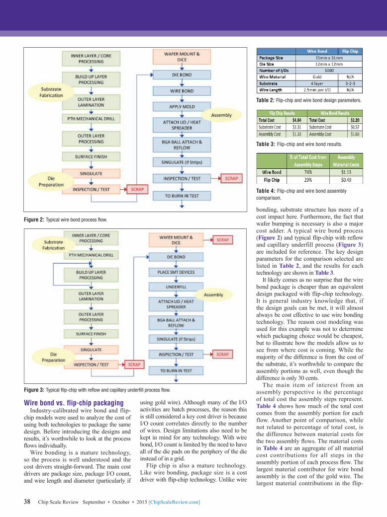
3838 Chip Scale Review September • October • 2015 [ChipScaleReview.com]
Wire bond vs. flip-chip packagingIndustry-calibrated wire bond and flip-
chip models were used to analyze the cost of using both technologies to package the same design. Before introducing the designs and results, it’s worthwhile to look at the process fl ows individually.
Wire bonding is a mature technology, so the process is well understood and the cost drivers straight-forward. The main cost drivers are package size, package I/O count, and wire length and diameter (particularly if
using gold wire). Although many of the I/O activities are batch processes, the reason this is still considered a key cost driver is because I/O count correlates directly to the number of wires. Design limitations also need to be kept in mind for any technology. With wire bond, I/O count is limited by the need to have all of the die pads on the periphery of the die instead of in a grid.
Flip chip is also a mature technology. Like wire bonding, package size is a cost driver with fl ip-chip technology. Unlike wire
bonding, substrate structure has more of a cost impact here. Furthermore, the fact that wafer bumping is necessary is also a major cost adder. A typical wire bond process (Figure 2) and typical flip-chip with reflow and capillary underfill process (Figure 3) are included for reference. The key design parameters for the comparison selected are listed in Table 2, and the results for each technology are shown in Table 3.
It likely comes as no surprise that the wire bond package is cheaper than an equivalent design packaged with flip-chip technology. It is general industry knowledge that, if the design goals can be met, it will almost always be cost effective to use wire bonding technology. The reason cost modeling was used for this example was not to determine which packaging choice would be cheapest, but to illustrate how the models allow us to see from where cost is coming. While the majority of the difference is from the cost of the substrate, it’s worthwhile to compare the assembly portions as well, even though the difference is only 30 cents.
The main item of interest from an assembly perspective is the percentage of total cost the assembly steps represent. Table 4 shows how much of the total cost comes from the assembly portion for each flow. Another point of comparison, while not related to percentage of total cost, is the difference between material costs for the two assembly fl ows. The material costs in Table 4 are an aggregate of all material cost contributions for all steps in the assembly portion of each process fl ow. The largest material contributor for wire bond assembly is the cost of the gold wire. The largest material contributions in the flip-
Figure 2: Typical wire bond process flow.
Figure 3: Typical flip-chip with reflow and capillary underfill process flow.
Table 2: Flip-chip and wire bond design parameters.
Table 3: Flip-chip and wire bond results.
Table 4: Flip-chip and wire bond assembly comparison.
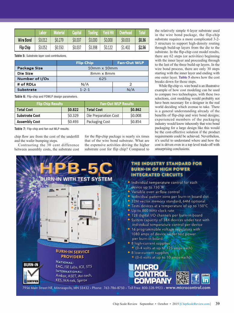
3939Chip Scale Review September • October • 2015 [ChipScaleReview.com]
chip fl ow are from the cost of the underfi ll and the wafer bumping steps.
Contrasting the 30 cent difference between assembly costs, the substrate cost
for the fl ip-chip package is nearly six times that of the wire bond substrate. What are the expensive activities driving the higher substrate cost for flip chip? Compared to
the relatively simple 4-layer substrate used in the wire bond package, the flip-chip substrate requires a more complicated 3-2-3 structure to support high-density routing through build-up layers from the die to the substrate. In the fl ip-chip cost model results, there are 62 steps (or activities) beginning with the inner layer and proceeding through to the last of the three build-up layers. In the wire bond process, there are only 30 steps starting with the inner layer and ending with one outer layer. Table 5 shows how the cost breaks down for those steps.
While fl ip chip vs. wire bond is an illustrative example of how cost modeling can be used to compare two technologies, with these two selections, cost modeling would probably not have been necessary for a designer in the real world deciding which avenue to take. There is a general understanding already of the benefits of flip-chip and wire bond designs; experienced members of the packaging industry would know inherently that wire bond packaging for a large design like this would be the cost-effective solution if the product requirements could be achieved. Nevertheless, it’s useful to understand where and how the cost is driven even in a top level trade-off with unsurprising conclusions.
Table 5: Substrate layer cost contributions.
Table 6: Flip-chip and FOWLP design parameters.
Table 7: Flip-chip and fan-out WLP results.
4040 Chip Scale Review September • October • 2015 [ChipScaleReview.com]
Flip-chip vs. fan-out wafer-level packaging
The next example focuses on a smaller design that can be packaged using flip-chip or fan-out wafer-level packaging technology (FOWLP). The fl ip-chip process flow and a few of the highlights were already addressed. Before moving into the technology comparison, the FOWLP process flow is introduced in Figure 4. One of the clear advantages with this flow is that there are fewer steps, which makes for a simpler process. On the other hand, there are bigger yield risks associated with FOWLP. Once the die is placed, there is no opportunity to test and scrap until the very end of the fl ow. This means that any fabrication or assembly defects discovered at that point will require
scrapping the entire package, which may include expensive die as well. Similar to the two technologies previously introduced, package size is certainly a cost driver here. Another notable cost driver is the number of imaging steps. Unlike wire bond and fl ip-chip technologies, redistribution layers (RDLs) are required to distribute the package I/Os, and these require expensive lithography steps.
The key design parameters used to compare flip chip and FOWLP are outlined in Table 6); Table 7 lists the top-level results. In this case, flip chip is more cost effective than FOWLP but by a narrower margin than in the previous comparison. This fl ip chip vs. FOWLP example is also more of an apples to oranges comparison. While wire bond and fl ip chip are very different technologies, their process fl ows and costs still break down into assembly and substrate portions. FOWLP, on the other hand, doesn’t have two distinct portions of the process fl ow in the same way.
With the technologies being so different, it’s difficult to make direct comparisons in many areas. One of the more interesting ways to look at the detailed cost results is to compare RDL steps from the FOWLP fl ow
to build-up steps from the flip-chip flow. The creation of one RDL can be seen as similar to the creation of one build-up layer, in that each serves the same purpose from a substrate perspective. Table 8 shows the cost components associated with fabricating two RDL layers vs. two build-up layers. The largest contributions to the cost difference come from capital and yield considerations. Yield will be discussed in the following example. As for capital, the increased capital cost for FOWLP is because the lithography equipment required to create an RDL is more expensive than the equipment needed for the build-up portions of a flip-chip package.
The final set of numbers is an example of a key cost factor that should always be taken into account: yield. Table 9 summarizes how the cumulative yield is different for these two technologies even when the incoming yields are the same. The table shows the cumulative yield with the following incoming yield assumptions: 1) 90% die yield; 2) 90% fabrication yield; and 3) 90% assembly yield. To tie this to the design example already given in this section, the cost of the FOWLP package at different cumulative yields was calculated (Table 10). Note that with this design, if a yield of 95% is achieved, it becomes cost-competitive with the same design in a fl ip-chip package.
SummaryCost modeling is not only a useful tool
for determining the lowest cost choice to meet product requirements, but a necessity for understanding the cost drivers. With an understanding of technology cost drivers, everyone from designers to supply chain managers can make more cost-effective decisions.
The technology comparisons in this article provided examples of different ways cost modeling can be used. The wire bond and flip-chip comparison did not provide surprising results overall, but illustrated which characteristics of the process flows contributed to the notable cost difference. The fl ip-chip and FOWLP comparison was more interesting because the total cost results were closer. This made it an example of how cost-effective packaging choices depend heavily on design parameters.
BiographyAmy Palesko received her degree
in Chemistry from The College of William and Mary; she is VP of Business Development at SavanSys Solutions LLC; email [email protected]
Table 9: Yield comparison of flip chip and FOWLP.
Table 10: FOWLP results at different yield points.
Table 8: Cost components of RDL and build-up layers.
Figure 4: Typical FOWLP process flow.

4141Chip Scale Review September • October • 2015 [ChipScaleReview.com]
Bond tester study of CSP reliability through bump analysisEvstatin Krastev, Ian Christopher Mayes, Chan Myat, Armin Struwe [Nordson DAGE], Rene P. Zingg [Zinan GmbH], Ricardo Geelhaar [PacTech GmbH]
iniaturization, the drive to lead-free semiconductor products, combined with the increasingly harsh application environments
impose stringent requirements on solder bump reliability in chip-scale packages (CSP). In addition to a clear quality specification, there is a need for comprehensive mechanical testing to ensure reliable solder connections over the projected lifetime of the device. Such tests must detect problems and nonconformances as early as possible in the production cycle. A systematic approach to predict product lifetime, monitor ongoing production, process control statistical methods, and failure analysis is needed in order to guarantee high-quality product. While nondestructive tests like X-ray computer tomography are always desired, they cannot replace the information that can be deduced from standard mechanical bond test methods like shear and cold bump pull (CBP). This paper discusses CSP bump reliability in general, and various bond test methods in particular. A case study evaluating different solder compounds (Sn-0.7%Cu, Sn-3%Ag-0.5%Cu, Sn-3%Ag-0.7%Cu) is also presented in order to illustrate the methodology and discuss the challenges.
Discussion of bump failure modes in CSP packages
Open, intermittent contact in the final product is the major failure mode. This can be caused by delamination from excessive stress, coalescence of voids formed during assembly, undesirable intermetallic compounds (IMC) formed during reflow of the solder, or void formation through electromigration. Several root causes can also compound, e.g., when multiple IMCs with different electrical resistivity and/or voids cause current-crowding, thereby accelerating electromigration. These problems can be minimized by adequate process control, proper material choice, and design optimization to minimize stress from different coeffi cients of thermal expansion (CTE). It is important to note that even slight changes in alloy composition of the solder can have a large effect on its mechanical properties.
Shorts or leakage paths between bumps is another typical failure mode. Root causes for this are attributed to insufficient barrier by the underfill to whisker growth and surface contaminations leading to ionic or galvanic leakage paths. This mode is typically more related to underfi ll and cleaning than to bump composition and formation.
Process control Once the solder composition, pad size and arrangement, and substrate material (under-bump metal choice and thickness) are finalized from finite element modeling (FEM), the assembly process, and its expected variation over substrate space and time has to be considered and examined. Common methods include DoE for process parameters and their variation, x-ray tomography and mechanical cross-sections (saw and polish or focused ion beam). These need to be performed on virgin devices and after accelerated life tests, such as thermal cycling and electromigration testing. The goal of this type of study is to understand the microstructure of the bump (including grain structure, precipitates, phase boundaries, IMC formation at under bump metallization (UBM), and occurrence of voids). In addition comparing samples with and without underfi ll
will establish if the particular material used fulfills its task of stress attenuation and confi nement of bumps to prevent premature delamination. These qualification tests should be regularly repeated as a monitoring program, e.g. on a quarterly basis. In addition to this qualification and reliability monitoring program, a continuous process control system is needed and since no non-destructive tests exist, bump shear (BST) and bump pull test (BPT) before system assembly, as well as die shear (DST) and die pull testing (DPT) after assembly are wildly used. These tests are described in detail in various industry standards and publications. Brittle fail at the IMC interface, extensive voiding, pad lift, i.e., delamination of the metallization under the UBM, are all reject criteria commonly used by the industry. It is very important to test bump quality before and after CSP assembly. This double testing becomes instrumental when trying to distinguish between material defects and assembly-related weaknesses.
B o n d t e s t e r t e c h n i q u e s f o r evaluation of bump quality
The three most common techniques for evaluation of bump quality and integrity are bump shear (BST), cold bump pull (CBP)
M
Figure 1: Schematic representation of shear test. The resulting momentum on the bump base is shown as a red arrow; green triangles represent the resulting tensile and compressive forces on the bump base.

4242 Chip Scale Review September • October • 2015 [ChipScaleReview.com]
and hot bump pull (HBP). The HBP test was developed to study pad cratering failures as per IPC-9708 standard.
The HBP test is performed by soldering a pin to the solder ball using a pre-defined temperature profile and then performing a pull test. The nature of the grip allows the pull force to be orientated with respect to the pad, simulating real life service conditions. Additional information can be obtained by cyclic loading.
It is well known that BST has complex force distribution (Figure 1). In addition, the shear tool imposes a rotational moment proportional to shear force and standoff (shear height), which in turn results in a lifting force at the leading edge of the UBM/bump system.
BPT (Figure 2), on the other hand, uniformly distributes the test force over the bump base. While BST imposes a signifi cant pull stress only at the leading edge, CBP and HBP tests stress the whole UBM area, both at the IMC interface to the bump above and the pad structure below the UBM. To summarize the above discussion, both shear and pull tests need to be considered and used when designing the test plan. The shear test is more straightforward and easy to perform and automate, however, in many cases, the pull test provides additional valuable information and failure modes that may not occur in a simple shear test. There is a clear need to test components, materials and bonds under controlled conditions that generate failure modes similar to those observed in service. In general, bond testing involves pulling or shearing at relatively low strain rates. Solder joints often fail by ductile fracture of the bulk solder and other parts of the joint do not experience the stress levels they would see if the loading on the joint had been more rapid. All joints can be thought of as a chain where the links of the chain represent the various materials that make up the joint. A simple solder joint on a PC board comprises a number of links: bulk solder, an intermetallic layer at the interface with the bond pad, the bond pad, an adhesive layer between the bond pad, and the organic substrate and the substrate itself. The joint is only as good as its weakest link and at low strain rates this is often the bulk solder. It is well known that solders exhibit time-dependent deformation and that their yield point increases dramatically with strain rate. The much higher strain rates associated with impact and board bending result in much higher forces on the bond pad, as for these cases there is less time for the material to flow. High strain rates produce larger bond pad forces. Soldered connections can fail in a brittle manner at high rates of strain. Low strain rate testing cannot pick
up the microstructural changes that occur at the bond interface responsible for a brittle connection. Low strain rates cannot identify microstructural changes that lead to brittle fracture. Therefore, in order to study brittle fracture failures, we need to employ high strain rate testing in addition to the regular BST and CBP.
Case study: low-speed shear test of various SAC alloys
In order to illustrate the above discussions, we performed a simple bond tester study of various SAC solder alloys. Lead-free solders around the Sn-Ag-Cu eutectic point offer many
Figure 2: Illustration of a cold-bump pull (CBP) test. Force geometry is less complex than BST and a uniform tensile stress is projected over the bump base.
Figure 3: SAC305 solder bumps after fi rst refl ow as used in this study.
Figure 4: Test setup for BST testing. The wafer samples were secured using a vacuum wafer chuck.
IN-HOUSE PROCESSING
THERMAL OXIDATION
METAL SPUTTERING
METAL EVAPORATION
THICK RESIST PATTERN
CUSTOM PHOTORESIST PPATTERNING
FORMING GAS ANNEAL
25MM-450MM
IMAT specializes in Thermal Oxidation
and PVD Metal Deposition of silicon
wafers. IMAT also provides custom
patterned photoresist for a variety of
applications on 8” and 12” wafers.
Ask us about how we can help
streamline your tasks.
www.imatinc.com
QUALITY SILICON WAFER PROCESSING
SINCE 1995

4343Chip Scale Review September • October • 2015 [ChipScaleReview.com]
significantly stronger solder alloy. Thus, the Sn-Ag-Cu system can offer many interesting material property variations around its eutectic point (SAC, close to SAC378 or Sn-3.75%Ag-0.8%Cu). These can be effectively studied using the bond tester methods discussed above.
SummaryAs a general conclusion, we
want to reinforce that there is a clear need to test components, mate r ia l s and bonds under con t ro l l ed cond i t i ons t ha t generate failure modes similar to those observed in real life. A simple solder joint can fail due to multiple factors and the weakest link could be in the bulk solder, the intermetallic layer at the interface with the bond pad, the bond pad itself, the adhesive layer between the bond pad, and the organic substrate and the substrate itself. This implies that a test methodology comprising standard BST and BPT, as well as high strain rate testing and HBP, provide a comprehensive set
of test results that can be used to monitor quality and optimize design and materials. In addition, camera-assisted automation of the bond testing process permits large statistically significant data sets to be acquired in a short period of time, and minimizes operator dependency.
BiographiesEvstatin Krastev received his MS in
Electrical Engineering and PhD in Physics from Michigan State U.; he is Director of Applications at Nordson Dage; email [email protected]
Ian Christopher Mayes received his Bachelor of Metallurgy from Sheffi eld U. and PhD from Imperial College, London; he is a Technical Manager, Bond Test, at Nordson Dage. Chan Myat received his Bachelor Honours (BEng) degree in Electrical/Electronic Engineering at the U. of Hertfordshire and is a Bond Tester Application Engineer at Nordson Dage. Armin Struwe is European Sales Manager - Bond Test & Material Test at Nordson Dage. Rene P. Zingg received his PhD from Purdue U. and is a Consulting Engineer and co-owner at Zinan GmbH. Ricardo Geelhaar is a Unit Manager Production Wafer Level Packaging and Bumping at PacTech GmbH.
choices of parameters critical to assembly, such as melting point or range, thermal expansion coeffi cient, ductility or hardness. The specimen consisted of 125µm solder balls of SAC305 (Sn-3%Ag-0.5%Cu), SAC307 (Sn-3%Ag-0.7%Cu), SC07 (Sn-0.7%Cu) that were placed on pads of 120µm diameter. The under bump metal (UBM) consisted of 5µm-thick Ni coated with an Au anti-oxidation layer. After reflow, the solder balls formed 90µm-high bumps with a diameter of about 140µm (Figure 3), indicating a slight sag compared to a perfectly spherical bump (97µm-high, 134µm maximum diameter).
HBP tests showed exclusively solder failure, while CBP tests showed solder extrusion failures in some cases. We therefore concentrated on a simple shear testing experiment in order to evaluate the three different solder alloys. BST was performed using a 150µm-wide flat chisel at 500µm/s with a 10µm shear height (standoff). The wafers were secured using a vacuum wafer chuck. The test setup is shown in Figure 4 and a typical ductile failure mode is shown in Figure 5.
Figure 6 shows the shear test results on a normalized distribution plot. The narrow distribution indicates a fairly well controlled process with random process variation. Based on this, it can be concluded that SAC 305 and SC07 perform in a very similar way. However, only slight variation in composition (increasing Cu content by 0.2% in SAC307) results in a
Figure 5: Ductile failure of an SAC305 bump. The test speed was 500µm/s with a 10µm shear height (standoff).
Figure 6: Cumulative distribution of a ball shear test for three lead-free solder compounds.

4444 Chip Scale Review September • October • 2015 [ChipScaleReview.com]
Solving delamination in lead frame-based packages
By Rongwei Zhang, Yong Lin, Abram Castro [Texas Instruments Inc.]
e l a m i n a t i o n a t v a r i o u s interfaces in lead frame-based packages, such as small outline
integrated circuit (SOIC), thin-shrink small outline package (TSSOP), quad fl at package (QFP) and quad-flat no-leads (QFN), remains one of the most critical reliability issues in plastic-encapsulated IC packages. In plastic-encapsulated IC packages, there are many interfaces adhered together. These interfaces include mold compound to die, die to die attach material, die attach material to lead frame, mold compound to die pad, mold compound to lead fi nger, and die pad backside to mold compound in an SOIC package (Figure 1).
When an IC package is exposed to a humid environment, mold compound and die attach materials (polymer composites)
will absorb moisture in two ways: 1) through bulk mold compound, and 2) through interfaces between the mold compound and lead frame. This absorption will influence material properties in several ways; first, mold compound and die attach materials will expand, while the die and lead frame do not. This expansion induces the hygrostresses within packages. Second, the absorbed moisture can change the modulus and glass transition temperature (Tg) of polymer materials to lower values. Third, moisture ingress through the interface and accumulation of water at the interface will degrade the interfacial adhesion caused by water bonding to polymer chains, especially where secondary bond forces dominate the adhesion.
During system board assembly, if the plastic packages with absorbed moisture are subjected to a reflow process, large thermal stresses are induced along the interfaces owing to differences in the coefficient of thermal expansion (CTE) of the packaging materials. Meanwhile, as temperature increases during refl ow (peak temperature up to 260˚C), the absorbed moisture will vaporize resulting in a high vapor pressure, and the interfacial adhesion will further decrease. The combined effect of high vapor pressure, stresses, and decreased adhesion can lead to interfacial delamination and package cracking during refl ow (also known as “popcorning”). Therefore, the delamination at different interfaces is generally driven by the mismatch of different material properties such as CTE, hygro-swelling, vapor pressure-induced expansion during the refl ow process, and adhesion degradation caused by moisture absorption and/or temperature increase [1, 2]. Delamination at different interfaces is usually detected by C-mode
scanning acoustic microscopy (C-SAM), through transmission scanning acoustic microscopy (TSAM), and scanning electron microscope (SEM). Figure 2 is an example of detecting the delamination between die attach material and lead frame using SEM.
Factors affecting delaminationMany factors can contribute to interfacial
delamination in lead frame-based packages. These factors mainly include package structure, packaging material, assembly process, and reliability test condition. Factors contribute to the delamination at different interfaces could be different. Here, we will focus on polymer-based packaging materials and assembly process.
Package structure/geometry. Many package structure factors, such as package dimension (x, y, z), die dimension, die pad dimension, lead frame design, number of leads, the distance from die edge to pad edge, have a significant effect on package delamination. Packages with exposed die pad are more prone to delamination due to the unbalanced encapsulation of the package. This unbalanced encapsulation increases the mechanical stress at the die-to-die pad interface during IR refl ow, which can lead to an increase in die pad delamination [3].
Packaging materials . Packaging material properties play a key role in package delamination. In particular, CTE, modulus, the amount of moisture absorption, and moisture diffusion rate of both mold compound and die attach material are major factors contributing to the stress during reflow. Ideally, selecting the material with CTE equal or close to the bonding material, and with lower modulus, lower moisture absorption and fast diffusion rate would result in better delamination performance. Additionally, the ability of the package materials (mold compound and die attach material) to maintain their high adhesion strength post moisture absorption and thermal stress, is another important factor. By nature, polymer composite material properties are not ideal and have to be compromised to
D
Figure 1: Delamination at different interfaces in an SOIC package.
Figure 2: A SEM image of the interfacial delamination between die attach material and lead frame in a lead frame-based package.

4545Chip Scale Review September • October • 2015 [ChipScaleReview.com]
meet a specific manufacturing process and delamination requirement.
Examples of the tradeoff can be seen in both die attach material and mold compound. At fi rst thought, it would be ideal to select a low modulus die attach material to improve delamination performance; but if the material is used in conjunction with a copper wire bonding process, high bonding temperatures dictate that the die attach material have a relatively high modulus to prevent energy dissipation from the active bonding area. With respect to the mold compound, higher adhesion mold compound is preferred from a delamination point of view, but this is limited by the molding process—too high adhesion could result in manufacturability issues. Selecting or developing a polymer material with key balanced properties meeting a specific manufacturing process and delamination requirement is critical for successful material qualifi cation.
Assembly process. The assembly process is another key factor affecting delamination because packaging material properties can be signifi cantly changed by it. Examples are discussed below.
The delamination between die backside and die attach material can be affected by wafer backside surface roughness. The interfacial adhesion can be improved with higher roughness of the die backside thereby improving the delamination at the interface between die backside to die attach material.
In the die attach/cure process, several variables exist. The time between die attach paste dispense and die placement (open time), and the time between die placement and curing (staging time) are critical to prevent voiding and adhesion degradation. Curing temperatures and time will also drive differences in die attach material properties, resulting in the same die attach material demonstrating different delamination performances. Some lower curing temperatures may be applied to lower the modulus of die attach materials for large packages to absorb the stress, while in other cases, higher temperature may be applied to improve the adhesion. Other parameters in the die mounting process that result in different bond line thickness (BLT), fillet height and coverage of die attach materials will affect the delamination. Thicker BLT, higher fi llet height without contaminating the die surface, and more coverage are preferred to improve delamination.
Assembly innovations in wire bonding and molding have influenced die attach delamination in heretofore unobserved
ways. As the industry moves from gold wire to bare copper wire and palladium-coated copper wire (PCC), the impact of wire bonding processes on die attach delamination becomes increasingly s igni f icant due to h igher bonding temperature. This impact is accelerated as the industry moves toward larger lead frame strips (100mm x 300mm) and package miniaturization because the strips are exposed to more time at the higher wire
bond temperatures. During the molding process (typically transfer molding) at 175˚C, mold compound will cross-link and form polymer networks, which will decrease the mold compound volume (called “cure shrinkage”). Cure shrinkage will induce stresses. After molding, post-mold cure (PMC, typically at 175˚C for 3-6 hours) is performed to further cure the mold compound. During PMC, material properties are changed and further cure
[email protected] 9001
ISOTS 16949
Your Partner forAdvanced Packaging
Our Services
Wafer Bumping- UBM & OPM Plating, e.g. eless NiAu & NiPdAu, e-plate Cu & Au- NiFe Plating for MEMS- Solder Ball Attach / Solder Jetting- Wafer Level RDL (Low Volume)- CSP & BGA Ball Rework
Wafer Backside Metallization- Wafer Thinning- Single Wafer Etch- TiNiAg & TiNiAu Evaporation
Backend & Die Sort- Laser Marking, Sawing, Electrical Test- Tape & Reel- FC-Assembly

4646 Chip Scale Review September • October • 2015 [ChipScaleReview.com]
shrinkage can occur. Subsequent processes such as degating, defl ashing and singulation can exert high stress on the package and cause delamination.
External factors, such as contamination, from the assembly process can also induce delamination. Many contamination cases were reported to induce delamination at different interfaces. For example, the residuals transferred from back grind tape can cause die top to mold compound delamination. During the curing of die attach material, the deposit of outgassing from die attach material can contaminate the lead fingers and potentially cause the delamination at the interface of the mold compound to lead frame. Many technologies are available to detect the contaminants which include, but are not limited to, Fourier transform infrared spectroscopy (FT-IR), time-of-fl ight secondary ion mass spectrometry (TOF-SIMS), SEM, X-ray photoelectron spectroscopy (XPS), Auger electron spectroscopy (AES), and contact angle measurement.
Reliability test conditions. Package reliability tests that can induce delamination typically include moisture sensitivity level (MSL), thermal cycling, high-temperature storage, and autoclave. In these tests, different humidities, temperatures and other environmental factors, when applied to a package, can affect the material properties and interfacial adhesion to a different extent, and thereby resulting in different levels of delamination.
Impact of delaminationDelamination at different interfaces
can cause various failures, which are discussed below.
• Delamination between die active surface and mold compound (Figure 1a) can cause the ball bond to be mechanically lifted, thereby leading to electrical failure during thermal cycling. The delamination is a key trigger for passivation cracking, so delamination at the interface of the active die surface and mold compound is usually not allowed.
• Similarly, the delamination at the interface of the lead fi nger and mold compound (Figure 1b) can cause the stitch bond to break and result in an open circuit. Bare copper or PCC wires are more susceptible to broken stitching as they are harder than gold wire. Therefore, as bare Cu wire or PCC gets more popular in the industry, improving mold compound delamination (Figures 1a, b and e) becomes increasingly critical to manufacture reliable Cu wire-based packages. Moreover, as mold compound delamination occurs, moisture and contaminants (such as corrosive ion Cl-) can easily enter the package. With moisture, the mobility of corrosive ions like Cl- can signifi cantly increase, which will accelerate Cu wire corrosion and lead to electrical failures at ball bonds and stitch bonds. The mobile ions entering the package can also cause current leakage [1, 4].
• For thermally enhanced packages, there is a thermal requirement. Die attach delamination (Figures 1c and d), which includes the delamination at the interface between the die and die attach material and between die attach material and lead frame (Figure 2), reduces the contact area of the die to the lead frame, and therefore, increases the thermal resistance of the package. As a result, if the die operating temperature exceeds the maximum junction temperature, the device can shut off because of overhea t ing . The maximum acceptable percentage of delamination will be highly dependent on device power and power distribution over the die surface [5, 6].
It should be pointed out that not all types of delamination are a major reliability problem. The delamination between the mold compound and die pad (Figure 1e) may not be regarded as serious if there is no down bond on the die pad. With down
bonds, the delamination between the mold compound and the die pad should be avoided. Because of the CTE differences between the die pad, the silicon die, and the mold compound, the movement of mold compound can cause the wires to break.
Solving delamination In order to manufacture a reliable and
robust package without delamination, many factors, such as package design, packaging materials, assembly process, environmental or application conditions, are needed to be carefully considered and optimized. There are many approaches to improve the adhesion and thereby solving the delamination problem, or at least improving the delamination performance. These approaches include selecting or developing new packaging materials, creating dimples/grooves/holes on the lead frame, plasma cleaning, modifying lead frame surface chemistry, such as coating the lead frame with adhesion promoters, and roughening the lead frame.
• Selecting new packaging materials is the typical way that industry takes to eliminate the delamination. In many cases, however, there is a limited choice of materials. Additionally, existing commercial materials may not be ful ly optimized to meet specific applications and therefore, may offer margina l re l iab i l i ty performance, while developing new materials is typically very time- and resource- consuming.
• A n o t h e r w a y t o i m p r o v e t h e delaminat ion is to incorporate var ious s t ruc tures on the lead frame surface, such as dimples, grooves and through-holes , to enable mechanical interlocking and enhance adhesion. Examples of lead frames with different features a re shown in Figure 3 . These mechanical enhancements do not require a change in packaging materials, but may not be applicable
Figure 3: Examples of lead frames with a) dimples, b) grooves, and c) through-holes. Figure 4: SEM images of the surfaces of a) a standard lead frame, and b) a roughened lead frame.
4747Chip Scale Review September • October • 2015 [ChipScaleReview.com]
to small packages where there is not enough space to make structures. Fur thermore , i f the fea ture of the structure is too small, there may be concerns wi th respec t to manufacturing and filling the structure with mold compound.
• From a process standpoint, plasma cleaning seems to be the most convenient process to implement. The most commonly used gases for plasma cleaning are argon (Ar), oxygen (O2) and their mixtures. In many cases, plasma is applied post wire bonding to remove the contaminants and enhance the wettability, thereby improving adhesion. But in other cases, the improvements may not be significant enough to eliminate the delamination, especially on a NiPdAu lead frame surface. Additionally, plasma cleaning may not be a feasible way to improve die attach delamination. Plasma cleaning increases the surface energy of the lead frame, which will make die attach pastes more prone to bleeding.
• Modi fy ing lead f rame sur face chemistry has been used to improve delamination. Oxidizing Cu surfaces of a Cu lead frame is one way to modify the surface and improve the adhesion through enhanced chemical interaction between the mold compound and the Cu lead frame, and increased surface roughness. It is observed that maximum adhesion strength was obtained when the oxide thickness is about 20nm [7]. Further oxidation to increase oxide thickness will dramatically decrease the adhesion. Alternate methods include coating lead frames with an adhesion promoter. An adhesion promoter is typically a bifunctional molecule, with one functional group interacting with the lead frame and the other with the mold compound and/or die attach material. Selecting the right functional groups that can strongly bind to the metal lead frame and cross-link with the mold compound and die attach to form covalent bonds is key to improving the adhesion. Spraying the adhesion promoter post-wire bond is a typical process because applying an adhesion promoter before the die attach process can lead to a wire bonding issue called non-stick on pad (NSOP).
• Another effective way to improve mold compound and die at tach
adhesion is to roughen the lead frame surface. This can be done through a plating process, etching process, or laser texturing [8]. These processes enhance mechanical interlocking and increase surface contact area. Figure 4 shows the surface comparison between a standard NiPdAu lead frame and a roughened NiPdAu lead frame. The roughened lead frame is typically coated with an
anti-resin bleed out (RBO) material to prevent resin bleed out. The disadvantage of a roughened lead frame includes higher cost and the potential requirements for process and material optimization to meet the manufacturability requirements. A future lower cost option might be achieved through the use of laser texturing based on the proliferation of laser techniques in the industry.
PPPRoHS

4848 Chip Scale Review September • October • 2015 [ChipScaleReview.com]
SummaryDelamination remains a challenging
issue in semiconductor packaging industry. This art icle provided the understanding of how delamination occurs, factors affecting delamination, impact of delamination, and methods utilized to solve the problem. Several of these methods may be combined to provide solutions. In particular, roughening the surface, combined with other methods as needed, seems to be the most effective and promising way to eliminate delamination. With a roughened lead frame, low cost mold compound and die attach materials can potentially be used to lower the total package cost while improving delamination. Meanwhile, with a roughened lead frame, thinner BLT of die attach material can be implemented to improve package thermal performance without affecting delamination, which also reduces the cost because of a smaller amount of materials used. These will be promising solutions to the delamination challenge to meet the requirements of package reliability, performance and cost.
References1. W. D. Van Driel, et al., “Prediction
of delamination in microelectronic packages,” 2005 IEEE 6th Inter. Conf. on Elect. Packaging Tech., pp. 1-6.
2. A. A. O. Tay, et al., “A study of delamination growth in the die-attach layer of plastic IC packages under hygrothermal loading during solder reflow,” IEEE Trans. on Device and Materials Rel., 2003, Vol. 3, pp. 144-151.
3. TI Application Report, “Moisture-sensitivity classification of flange-m o u n t e d p a c k a g e s a t Te x a s Instruments.”
4. J . McLeish , e t a l . , “Ensur ing suitability of Cu wire bonded ICs for automotive applications,” Chip Scale Review, 2014, pp. 18-21.
5. A. Chowdhury, et al., “The effect of die attach layer delamination on the thermal performance of plastic packages,” Elect. Comp. & Tech. Conf., 1998, 48th IEEE, pp. 1140–1147.
6. L . H . Meng , e t a l . , “Thermal s imulat ion s tudy of die at tach
delamination effect on TQFP package thermal resistance,” Elect. Mfg. Tech. Symp. (IEMT), 2010 34th IEEE/CPMT Inter., pp. 1–6.
7. E. Takano, et al., “The oxidation control of copper lead frame package for prevention of popcorn cracking,” 1997 IEEE 47th Elec. Comp. and Tech. Conf., pp. 78-83.
8. J. Fauty, et al., “Mold compound adhesion to bare copper lead frames-effect of laser texturing,” The Inter. Jour. of Microcircuits and Elect. Pkg., 2002, Vol. 25, pp. 51-79.
BiographiesRongwei Zhang received his PhD in
Chemistry from the Georgia Institute of Technology and is a Packaging Engineer at TI; email [email protected]
Yong Lin received his BS in Mechanical Engineering from Purdue U. and is a Packaging Engineer at TI.
Abram Castro received his BS in Electrical Engineering from Texas A&M U. and is a Material Platform Manager at TI.
MORE PERFORMANCE High-frequency (>40 GHz) sockets with a variety of materials to meet diverse testing requirements from Bench Characterization to Fully Automatic Handlers (>500k cycles) delivering what you need.MORE CHOICES Industry’s widest available DUT interfaces – Spring Probes, Microstrip™ Contacts and two types of
Conductive Elastomers.LESS COST All DUT interface materials available in off-the-shelf molded plastic for a fraction of other’s machined housing cost.LESS WAIT Aries can deliver the exact sockets you need in four weeks or less! So why settle?
Bristol, PA 19007-6810Tel 215-781-9956 • Fax 215-781-9845Email: [email protected]
A lot more of what you need...
...a lot lessof what you don’t!
The Evolution ofInterconnect Innovation
7582.indd 1 5/22/13 10:08 PM

4949Chip Scale Review September • October • 2015 [ChipScaleReview.com]
Performance of optimized lithography tools and materials in advanced packaging applicationsBy Keith Best [Rudolph Technologies, Inc.]
ecent years have seen rapid development in the area of advanced packaging. In
general, advanced packaging processes are concerned with the interconnection of multiple chips in a single package to provide increased functionality and performance in a smaller volume. Often advanced packaging processes are adaptations of front-end processes. Their development is being driven primarily by the rapid growth in mobile handheld devices such as smartphones. A number of technologies are in development or in production including wafer-level chip-scale packaging, copper pillar bumps on through-silicon vias (TSVs), fan-out wafer-level processing (FOWLP), and many more.
One technology that has gained rapid acceptance is 2.5D packaging. Similar to the multi-chip-modules (MCMs) of the past, 2.5D packaging processes use an interposer to route signals between the device die and the package substrate. The interposer is a multilayered “circuit board” fabricated on a silicon substrate and using through-silicon vias to pass signals from multiple die to the package substrate. 2.5D packages using high-density interposers can be a cost-effective, high-performance alternative to signifi cantly more complex 3D or system-on-chip (SoC) integration schemes. Most estimates project growth for 2.5D/interposer packaging faster than the industry as a whole.
A k e y e n a b l i n g t e c h n o l o g y f o r interposers has been the development of copper pillar bump technology to provide the high-density interconnection between the interposer and the die. Copper pillar bumps provide a number of advantages over the solder bump technology they are supplanting. They can deliver fi ne pitches down to 50μm in-line and 40/80μm when staggered. They can reduce costs by reducing the number of layers required in the substrate. They provide superior electromigration performance for high-
current carrying capacity applications. They permit electrical test at wafer-level prior to copper pillar bump. They are compatible with bond pad opening/pitch and pad metallization of die designed for wire bond, which enables quick time-to-market for conversion to fl ip chip.
Lithography challenges for 2.5D integration
Lithography is a key component of 2.5D integration schemes, however the requirements for interposer exposure systems differ significantly from the requirements of front-end lithography tools. In particular, 2.5D lithography faces specifi c challenges in regard to resolution, overlay, sidewall angle, exposure fi eld size, depth-of-focus, warped substrate handling and backside alignment.
Current resolution requirements are in the single-digit micron range. The need for sub-micron resolution is not anticipated in the foreseeable future. A suitable lithography systems should offer an N/A of 0.1 to 0.15 in order to meet the line/space (L/S) resolution requirement while also preserving a reasonable depth-of-focus (DOF).
Overlay is a combinat ion of the following: stage accuracy and repeatability; alignment microscope capabili t ies; translation, rotation and magnification compensation. As a rule of thumb, overlay accuracy should be about one-third of the resolution limit of the optical system. For interposer applications with a resolution limit of 1.5µm, overlay accuracy should be at least 0.5µm. Full-fi eld exposure systems, as well as 1x steppers, are typically limited in overlay accuracy, resulting primarily from their use of a double telecentric optical system that prevents them from compensating for magnification errors. A single-sided telecentric lens system combined with a 6-axis reticle positioning system provides complete freedom to adjust for optical errors, including real-time variations, such as those caused by thermal
expansion.When processing thick photoresist or
photo-defi nable dielectrics, well controlled sidewall angles are a critical requirement, and in some cases, a challenge. Although sidewall angles are primarily a function of the photosensi t ive material and its processing (pre-bake, post-bake, developing, etc.), the exposure system plays an important role. Accurate focus control across the wafer or substrate is required to achieve tight CD control and consistent sidewall behavior.
One of the most important reasons why sub-micron front-end lithography systems, such as deep-ultraviolet (DUV) steppers and scanners, are not suited for interposer manufacturing is their limited depth-of-focus, a design tradeoff made to obtain the high numerical apertures required to resolve features measured in tens of nanometers. Without a DOF in the 10µm or greater range, patterning the thick layers used in 2.5D integration is challenging at best.
The exposure field size is yet another important parameter for interposer manufacturing. The size of the exposure fi eld should at least cover the full interposer. Although it is possible to stitch multiple exposures together, stitching is inherently slow and imposes a signifi cant throughput penalty. Although there are no standard interposer sizes, they tend to get larger as they combine and interconnect more chips and passive components.
I n t e r p o s e r s h a v e t h r o u g h - v i a interconnects from the top side to the bottom side. The lithography step to define via locations must be referenced to the other side of the wafer or substrate—so called front-to-back alignment. In the case of silicon, an infrared microscope is required to look through the substrate and see backside features.
Double-side processing causes substantial substrate warpage that front-end lithography systems are not designed to handle. Their limited depth-of-focus adds to this problem. Equipment solutions with warped handling
R

5050 Chip Scale Review September • October • 2015 [ChipScaleReview.com]
features, such as switchable and compliant vacuum gaskets on chucks and handlers, are needed for lithography and other processing steps. Equally important is “on-the-fly” focusing that adjusts the wafer position at each exposure to obtain optimal focus.
Cu pillar bump exampleLithography for copper pillar bumps
can be particularly challenging. The pillars are electroplated into openings in a thick layer of photoresist. The exposure system must provide the resolution to create the fi ne-pitched openings while at the same time delivering suffi cient depth-of-fi eld to expose through the full layer, maintaining top and bottom CDs and straight perpendicular side walls.
The work described below was performed using a JetStep® lithography system and the latest generation photoresist PMER P-CE5000 from TOK. The photoresist is specifically optimized for this application, offering signifi cant performance advantages when compared to the previous generations, including robust crack resistance, high leach resistance during electroplating, large
single-coat film thickness range, uniform coating thickness over topography, and imaging of vias with high-aspect ratios.
The photoresist film thickness in this example is 50μm. It was soft-baked for 300 seconds at 145°C, post-exposure baked (PEB) for 180 seconds at 100°C, and developed with TMAH 2.38%, 4 X 60 second puddle. The exposure pattern consisted of groups of holes, with all the holes in each group having the same diameter. Different groups had different diameters, ranging as low as 50μm. Some holes were “photocleaved” by precisely positioning a slit in the reticle over the holes during an additional exposure step, thereby exposing the side walls for inspection when developed (Figure 1). Focus and exposure were varied to create a classic focus exposure matrix. View the depth-of-focus, process window and exposure fi eld size results in Figures 2-4.
SummaryWe have discussed the dramatic growth in
advanced packaging processes, in particular 2.5D processes that use silicon interposer
and copper pillar bumps. Although many of the processes used in the process are similar to front-end processes, the differences are significant. Requirements for advanced packaging photolithography were reviewed and we looked at an example of the photolithography process used to define the copper pillars. The example used an exposure tool and photoresist specifically optimized for advanced packaging processes. It demonstrates very good performance and process latitude for both CDs and sidewall angle on a 50μm-thick fi lm.
AcknowledgementsThe author would like to thank TOKYO
OHKA KOGYO CO., LTD. (TOK) and the Rudolph Lithography Systems Group application team.
BiographyKeith Best received his BS degree from
the U. of Greenwich, and is the Director of Lithography Applications Engineering a t R u d o l p h Te c h n o l o g i e s ; e m a i [email protected]
Figure 1: The exposure pattern and the technique of “photocleaving” to provide cross-sectional views of the developed holes. Photo courtesy of TOK.
Figure 2: Top-down and cross-sectional view of several holes at different focus values with top and bottom diameter. Top and bottom diameters, and sidewall angle are also plotted at the bottom of the figure. Photo courtesy of TOK.
Figure 3: Top and bottom CDs for all exposure values plotted against the process window.
Figure 4: The optimal values for both top and bottom are identified as 112μm DOF and 15% exposure latitude.
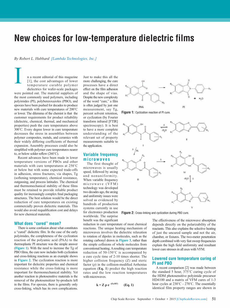
5151Chip Scale Review September • October • 2015 [ChipScaleReview.com]
New choices for low-temperature dielectric films
By Robert L. Hubbard [Lambda Technologies, Inc.]
n a recent editorial of this magazine [1], the cost advantages of lower temperature curable polymer dielectrics for wafer-scale packages
were pointed out. The material suppliers of the most commonly used polymers, including polyimides (PI), polybenzoxazoles (PBO), and epoxies have been pushed for decades to produce new materials with cure temperatures of 200˚C or lower. The dilemma of the chemist is that the customer requirements for product reliability (dielectric, chemical, thermal, and mechanical properties) push the cure temperatures above 300˚C. Every degree lower in cure temperature decreases the stress in assemblies between polymer composites, metals, and ceramics with their widely differing coefficients of thermal expansion. Assembly processes could also be simplifi ed with polymer cure temperatures nearer to, or below solder refl ow (260˚C).
Recent advances have been made in lower temperature versions of PBOs and other materials with cure temperatures at 250˚C or below but with some expected trade-offs in adhesion, stress fractures, via shapes, Tg (softening temperature), chemical resistance, outgassing, and process latitudes. The chemical and thermomechanical stability of these films must be retained to provide reliable product quality for increasingly complex fi nal packaging structures. The best solution would be the direct reduction of cure temperatures on existing commercially proven dielectric materials. This would also avoid requalifi cation cost and delays for new chemical materials.
What does “cured” mean?There is some confusion about what constitutes
a “cured” dielectric film. In the case of the early polyimides, the completeness of the cyclization reaction of the polyamic acid (PAA) to the thermoplastic PI structure was the simple answer (Figure 1). With the need to increase the Tg of PBO fi lms, the cure now includes both cyclization and cross-linking reactions as an example shows in Figure 2. The cyclization reaction is more important for dielectric properties and chemical resistance while the cross-linking is more important for thermomechanical stability. Yet another reaction in photosensitive materials is the removal of the photosensitizer by-products left in the films. For epoxies, there is generally only cross-linking, which has its own complications.
Just to make this all the more challenging, the cure processes have a direct effect on the fi lm adhesion and the shape of vias. Despite the new complexity of the word “cure,” a film is often judged by just one measurement, say Tg, percent solvent retention, or cyclization (by Fourier transform infrared [FTIR] spectroscopy). It is best to have a more complete understanding of the relevant set of property measurements suitable to the application.
Variable frequency m i c r o w a v e s
The first thought of microwaves is usually speed, followed by arcing and nonun i fo rmi ty. When variable frequency m i c r o w a v e ( V F M ) technology was developed two decades ago, the arcing and uniformity issues were solved as evidenced by hundreds of production systems currently in use for electronics production worldwide. The surprise benefi t was the signifi cant reduction in cure temperature of most chemical reactions. The unique heating mechanism of microwaves involves the dielectric relaxation to rotation of dipoles in molecules, such as the rotating carbonyl drawn in Figure 3, rather than the simple collisions of whole molecules from conventional heating. A resulting cure temperature reduction of 50-150˚C is accompanied by a cure cycle time of 2-10 times shorter. The higher collision frequency (Z) and steric factor (ρ) in the collision-modified Arrhenius equation (Eq. 1) predict the high reactionrates and the low reaction temperatures with microwaves.
k = Z ρ e –(Ea/RT) (Eq. 1)
The effectiveness of the microwave absorption depends directly on the polarizability of the reactants. This also explains the selective heating of just the uncured sample and not the air, chamber, or fi xtures. The two-meter penetration depth combined with very fast sweep frequencies explain the high field uniformity and resultant lower cure stresses in all axes with VFM.
Lowered cure temperature curing of PI and PBO
A recent comparison [2] was made between the standard 5 hour, 375˚C curing cycle of the HDM photosensitive polyimide precursor HD4100 and a matrix of VFM cures of 1-3 hour cycles at 230˚C - 270˚C. The essentially identical film property ranges are shown in
IFigure 1: Cyclization reaction of PI cure.
Figure 2: Cross-linking and cyclization during PBO cure.

5252 Chip Scale Review September • October • 2015 [ChipScaleReview.com]
which could be an amine, anhydride, or phenol. The important feature is that the starting materials are monomers (or short ionomers) that react with each other to make a highly cross-linked product resembling a chain link fence. As dielectric fi lms, the “epoxies” have much higher moduli (harder) and much lower elongation to break than the long chain PI and PBO fi lms. They are also less expensive and lower in cure temperature and Tg. Often they incorporate elastomers or elastomer fi llers to improve their stress properties, and silica filler to improve CTE values. With Tg values of 100-150˚C and cure temperatures of 150-250˚C, they fi ll the need for temperature-sensitive processes with a trade-off of thermal, chemical and mechanical stability.
It is important to understand the term “cure” again here. As the two components react to form links, there is a point in time (and temperature) that they become substantially rigid, called gelation. At this point, there is so much chemical rigidity that further reactions between unreacted components and between chains that the rate of cure drops rapidly and finally stops. A “fully cured” thermoset may only be 50% reacted, but there is not enough mobility either between chains or agglomerations that no further reactions can take place at that temperature. Measurement of the Tg at this point is a maximum and is referred to as “ultimate” (Tg∞). Only by raising the cure
Figure 4. This photosensitive PI precursor is an example of cyclization cure. As an example of the speed of the VFM process, it was previously reported [3] that the same HD4100 could be cured with identical film properties at 350˚ in only fi ve minutes. Another polyimide precursor, PI 2611 (HDM), produces a unique PI fi lm with a coeffi cient of thermal expansion (CTE) of only 5ppm/ C to match that of silicon. VFM cure of PI 2611 has been reported at 200˚C with a CTE of 3ppm/ C [4].
The more complex “cure” of a conventional low-temperature PBO was studied to determine the relative contributions, or even competition,
between cyclization and cross-linking as portrayed in Figure 2. Comparisons were made using a time at the highest soak temperature of 30 minutes for both oven and VFM as depicted in Figure 5. The cyclization (Figure 6) by oven cure is only 70% complete at 200˚C even if the soak time is increased to 60 minutes. It can be seen that VFM achieves a 96% cyclization by 200˚C with the 30 minute soak. The cyclization with VFM cannot be said to significantly increase between 200˚C and 250˚C considering measurement error at this level. The extent of cyclization in both cases is directly measured with FTIR by comparing the decrease in the amide peak of the starting material to a phenyl absorption that is a constant reference.
The cross-link reaction is more complex, and might better be considered mostly a chain-extension process. For several reasons, the extent of cross-linking was measured by FTIR as an adjusted ratio of the decrease of the cross-linker to the phenyl reference absorption as shown in Figure 7. Cross-linking in the oven appears to increase steadily up to 250˚C, whereas the VFM cured samples increased to more than twice that level by 200˚C and leveled off. It appears that even though the cyclization is essentially complete at 200˚C by VFM, the chains are getting longer at the same rate and are also finished at 200˚C. The potential “competition”
between cyclization and cross-linking as suggested in Figure 2 may no t be a s significant with the VFM cure process. All of this data refers to a 30-minute soak, so it would be interesting to see if these reactions w o u l d b o t h b e completed with VFM at temperatures below 200˚C with longer soak times.
Epoxies are a ver y d i f ferent matter
The term “epoxy” is often used when referring to other highly cross-linked t h e r m o s e t s l i k e polyhdroxystyrenes and novolacs as well as mixtures with a percentage of epoxides added. There are two basic components to an “epoxy” mixture, including an epoxide resin and a “curing agent” or “hardener,”
Figure 3: Dipole rotation heating mechanism of microwaves.
Figure 4: Film property comparison of oven and VFM cure of PI (HD4100).
Figure 5: Cure process profi les for oven and VFM cure of a PBO.

5353Chip Scale Review September • October • 2015 [ChipScaleReview.com]
temperature could the Tg∞ be increased, but at the risk of decomposition. The cure temperature of thermosets is therefore always chosen higher than the Tg∞. This is important because if the fi lm is not fully cured, but is taken to a higher temperature later, for example at solder refl ow, the Tg∞ will change and the fi lm properties will change. If the cure temperature is chosen below the Tg∞, the material will return to a glassy solid (vitrify). At this point, the rate of cure drops by 2-3 orders of magnitude (stops) as shown by the grey area in Figure 8 [5]. Another reason to set the cure temperature above Tg∞ is to accomplish adhesion at all surfaces. All of this is important to understand to avoid failures or hidden problems in assemblies with multiple heating steps.
With this background, it should be very surprising to read recent articles about VFM curing of epoxy underfi lls. At ECTC-2010 this author produced data showing epoxy underfill curing with VFM at cure temperatures well below the Tg∞ with lowered warpage, lowered modulus, and full cure (Tg∞) [6]. With careful DOEs (statistically designed experiments), and two different underfi ll chemistries (Henkel FP4527 and UF 8830) it was shown that cure temperatures of 85˚C could replace the standard cure temperature of 165˚C and produce 20%-88% lower warpage of substrates and dice. The storage modulus (e below Tg) of UF 8830 with VFM was 3X lower than the oven cure at 165˚C, which indicates a 3X lower cross-link density (3X longer chain lengths). Later publications confi rmed that Namics and ShinEtsu underfi lls performed similarly. IBM followed in 2013 [7] with a comparison of three underfi lls cured with oven and VFM to fi nd 22% lower warpage and twice the reliability of a microprocessor package. Their cure was at 110˚C rather than 165˚C, and the modulus was reduced by 30%. They attributed the lowered warpage and increased reliability to the lower VFM cure temperature and the reduction in modulus.
The relationship of stress to cure temperature of thermosets can be seen in Figure 9 where the shrinkage in the solid state (from gelation back to room temperature) is directly proportional to that temperature difference [8]. Now
Figure 6: Cyclization of a PBO with oven and VFM curing to 250˚C.
Figure 7: Cross-linking of a PBO with oven and VFM curing to 250˚C.
Figure 8: Phase diagram of thermoset curing.
Specialty Chemicals for your Total Electronics Solution
1.800.888.0698ellsworth.com
Ask theGlue Doctor®
Adhesives
Sealants
Conformal Coatings
Potting Material
Thermal Management

5454 Chip Scale Review September • October • 2015 [ChipScaleReview.com]
VFM technology is used for production microelectronics processing already and is now moving to high-volume production at the wafer scale.
References1. C. Blatt, L. Shon-Roy, “The business of wafer-level packaging
polymers,” Chip Scale Review, July-Aug. 2015.2. M. P. Zussman, R. L. Hubbard, “Properties and characteristics of
HD4100 PSPI cured at 250˚C with microwaves,” Proc. of the 16th Symp. on Polymers for Microelectronics, Wilmington, DE, 2014.
3. M. P. Zussman, R. L. Hubbard, K. Hicks, “Rapid cure of polymer coatings for packaging applications,” Proc. of the 13th Symp. on Polymers for Microelectronics, Wilmington, DE, 2008.
4. R. L. Hubbard, B. Lee, “Reduced stress and improved 2.5/3DIC process compatibility with stable polyimide dielectrics,” Proc. of the Inter. Wafer Level Packaging Conf.,San Jose, Nov. 2013.
5. J. B. Enns, J. K. Gillham, “Time-temperature-transformation (TTT) cure diagram: Modeling the cure behavior of thermosets," J. Appl. Polym. Sci. 28, 2567 (1983).
6. R. L. Hubbard, P. Zappella, “Low warpage flip-chip underfill curing,” IEEE Trans. on Comp., Packaging and Mfg. Tech., Vol. 1, No. 12, Dec. 2011.
7. M. Diop, M. Paquet, “Interactions between variable frequency microwave underfi ll processing and high-performance packaging materials,” Proc. of the Inter. Microelectronics and Pkg. Society, San Diego, CA, 2013.
8. Fisch and Hoffman, “Reaction mechanisms, chemical structures, and changes in properties during the curing of epoxy resins,” Plastics Technology, Aug. 1961.
9. R. L. Hubbard, I. Ahmad, K. Hicks, “Reduced wafer warpage and stress in JSR dielectric fi lms,” Proc. of the Inter. Wafer Level Pkg. Conf., Santa Clara, CA, 2009.
Biography Robert L. Hubbard received his BS in Chemistry at Oregon State U. and his PhD in Organic Chemistry at Texas A&M U.; he is Director, Technology Development, at Lambda Technologies, Inc.; email [email protected]
the VFM cure temperature can be lowered without vitrifi cation and leaving incomplete cure. At lower cure temperatures, several commercial epoxy adhesives have been VFM-cured and shown to have signifi cantly lower cross-link density (modulus).
The use of VFM curing on three JSR epoxy-based dielectric films was shown [9] to reduce cure temperature from 250˚C to 160˚C with a reduction in wafer bow of 50%. The equivalent extent of cure was measured by the resistance to absorption of NMP solvent at 40˚C.
The exact mechanism for these effects in thermosets is under investigation, although the same results (lowered cure temperature and modulus) have even been found for ethylene-vinyl acetate rubbers, which involves a very different radical-based reaction mechanism.
SummaryA promising cost-effective method of reducing the cost of curing
polymer dielectrics would be to change the method of cure rather than changing (and qualifying) new chemistries. Even more effective would be if the lower cure temperatures could be performed with shorter cycle times. It would be better still if the fi lm properties were at least as good, and even better with regard to stress and warpage. With the use of variable frequency microwave technology, the cure temperatures of PI, PBO, and epoxy-based dielectric fi lms can be signifi cantly reduced, in shorter cure cycles, while achieving the same extent of cure. The unique heating mechanism of microwaves produces equivalent cyclization and cross-linking of these polymers, as well as assuring the same chemical and thermomechanical stability as the standard oven cure at higher temperatures. For cross-linked thermosets like epoxies, not only is vitrifi cation avoided at low cure temperatures, but lower modulus and lower cross-link density is produced.
OUR INNOVATIVE EQUIPMENT. YOUR COMPETITIVE EDGE.
“Manufacturing custom engineered equipment for over 25 years”
LED UV Irradiator
MEMS Dry Film Resist Laminator
Backgrind Tape Laminator
Backgrind Tape Remover
Wafer Mounter
Teikoku Taping System, Inc.5090 N 40th Street, Suite 140Phoenix, AZ 85018Office: 480.794.1926
www.teikoku-taping.com/en
Figure 9: Comparison in epoxy shrinkage between two cure temperatures.

5555Chip Scale Review September • October • 2015 [ChipScaleReview.com]
Stacked Memory Becomes a Reality
2.5/3D Products & Infrastructure
Competitive Technologies w/o TSV
Reserve your room at So�tel San Francisco Bay Hotel
Early registration rates end Nov. 24
Sponsor/exhibit opportunities available
Temporary Bonding & DebondingPresentations by: HD Micro, SUSS, Brewer, Dow, TOK
Interposer DesignPresentations by: Mentor, Cadence, Ansys
Half-day tutorials: Dec. 15 Special Technology Sessions
Special 3D Pioneer Award Hotel
Presented to:Prof. Mitsumasa Koyanagi, Tohoku
Dr. Peter Ramm, Fraunhofer EMFT
In recognition of their pioneering e�orts in TSV stacked 3DIC
(continued from page 36)References1. E. Davis, W. Harding, R. Schwartz, J.
Corning, “Solid logic technology: versatile, high performance microelectronics,” IBM Jour. of Research and Development, April 1964, pp. 102-114.
2. P. Totta, R. Sopher, “SLT device metallurgy and its monolithic extension,” IBM Jour. of R&D, May 1969, pp. 226-238.
3. J. H. Lau, Low Cost Flip Chip Technologies, McGraw-Hill Book Company, New York, 2000.
4. D. Love, L. Moresco, W. Chou, D. Horine, C. Wong, S. Beilin, “Wire interconnect structures for connecting an integrated circuit to a substrate,” US Patent no. 5,334,804, Date of Patent: Aug. 2, 1994.
5. F. Tung, “Pillar connections for semiconductor chips and method of manufacture,” US patent no. 6,578,754, Date of Patent: June 17, 2003.
6. F. Tung, US Patent no. 6,592,019, Date of Patent: July 15, 2003.
7. F. Tung, US Patent no. 6,681,982, Date of Patent: June 27, 2004.
8. http://www.asmpacifi c.com/asmpt/products_fl ipchip.htm.
9. A. Eitan, K. Hung, “Thermocompression bonding for fi ne-pitch copper-pillar fl ip-chip interconnect – tool features as enablers of unique technology,” Proc. of IEEE/ECTC, May 2015, pp. 460-464.
10. F. Nakano, T. Soga, S. Amagi, “Resin-insertion effect on thermal cycle resistivity of flip-chip mounted LSI devices,” ISHM Proc. of the International Symp. on Microelectronics, 1987, pp. 536-541.
11. Y. Tsukada, S. Tsuchida, Y. Mashimoto, “Surface laminar circuit packaging,” Proc. of IEEE/ECTC, May 1992, pp. 22-27.
12. J. H. Lau, T. Krulevitch, W. Schar, M. Heydinger, S. Erasmus, J. Gleason, “Experimental and analytical studies of encapsulated flip-chip solder bumps on surface laminar circuit boards,” Jour. of the Institute of Interconnection Tech., Vol. 19, No. 3, March 1993, pp. 18-24.
13. K. Gilleo, B. Cotterman, I. A. Chen, “Molded underfi ll for fl ip-chip in package,” Proc. of high-density interconnects, June 2000, pp. 28-31.
14. J. H. Lau, Q. Zhang, M. Li, K. Yeung, Y. Cheung, N. Fan, et al., “Stencil printing of underfill for flip chips on organic-panel and Si-wafer substrates,” IEEE Trans. on CPMT, Vol. 5, No. 7, July 2015, pp. 1027-1035.
15. C. P. Wong, D. Baldwin, M. B. Vincent, B. Fennell, L. J. Wang, S. H. Shi, “Characterization of a no-flow underfill encapsulant during the solder reflow process,” Proc. of IEEE/ECTC, May 1998, pp. 1253-1259.
16. M. Lee, M. Yoo, J. Cho, S. Lee, J. Kim, C. Lee, et al., “Study of interconnection process for fine-pitch flip chip,” Proc. of IEEE/ECTC, May 2009, pp. 720-723.
17. Y. Okayama, M. Nakasato, K. Saitou, Y. Yanase, H. Kobayashi, T. Yamamoto, et al., “Fine-pitch connection and thermal stress analysis of a novel wafer-level packaging technology using laminating process,” Proc. of IEEE/ECTC, May 2010, pp. 287-292.
18. K. Honda, T. Enomoto, A. Nagai, N. Takano, “NCF for wafer lamination process in higher density electronic packages,” Proc. of IEEE/ECTC, May 2010, pp. 1853-1860.
19. K. Honda, A. Nagai, M. Satou, S. Hagiwara, S. Tuchida, H. Abe, “NCF for pre-applied process in higher density electronic package including 3D-package,” Proc. of IEEE/ECTC, May 2012, pp. 385-392.
20. T. Fukushima, Y. Ohara, J. Bea, M. Murugesan, K.-W. Lee, T. Tanaka, M. Koyanagi, “Non-conductive film and compression molding technology for self-assembly-based 3D integration,” Proc. of IEEE/ECTC, May 2012, pp. 393-398.
21. Y. Ito, M. Murugesan, H. Kino, T. Fukushima, K. Lee, K. Choki, et al., “Development of highly-reliable microbump bonding technology using self-assembly of NCF-covered KGDs and multi-layer 3D stacking challenges,” Proc. of IEEE/ECTC, May 2015, pp. 336-341.
22. A. Choubey, E. Anzures, D. Fleming, A. Dhoble, L. Herong, R. Barr, et al., “Non-conductive film (NCF) underfill for flip-
chip assembly and high reliability,” Proc. of International Wafer-Level Packaging Conf., Nov. 2014, pp. 1-7.
23. D. Lee, K. Kim, K. Kim, H. Kim, J. Kim, Y. Park, et al., “A 1.2V 8Gb 8-channel 128GB/s high-bandwidth memory (HBM) stacked DRAM with effective microbump I/O test methods using 29nm process and TSV,” Proc. of IEEE/ISSCC, Feb. 2014, pp. 433-435.
24. J. Shin, Y. Kim, H. Lee, U. Kang, S. Seo, K. Paik, “Effects of thermocompression bonding parameters on joint formation of micro-bumps in non-conductive film (NCF),” Proc. of IEEE/ECTC, May 2015, pp. 910-915.
25. H. Lee, Y Choi, J. Shin, K. Paik, “Wafer-level packages (WLPs) using B-stage non-conductive fi lms (NCFs) for highly reliable 3D-TSV micro-bump interconnection,” Proc. of IEEE/ECTC, May 2015, pp. 331-335.
26. D. Hiner, D. Kim, S. Ahn, K. Kim, H. Kim, M. Lee, et al., “Multi-die chip on wafer thermocompression bonding using non-conductive fi lm,” Proc. of IEEE/ECTC, May 2015, pp. 17-21.
27. M. Li, D. Tian, Y. Cheung, L. Yang, J. H. Lau, “A high-throughput and reliable thermal compression bonding process for advanced interconnections,” Proc. of IEEE/ECTC, May 2015, pp. 603-608.

5656 Chip Scale Review September • October • 2015 [ChipScaleReview.com]
MICROELECTRONICS SYMPOSIUM
BIG ISLAND, HAWAII JANUARY 25-28, 2016
Share Your Research - Submit an Abstract Today!
www.smta.org/panpac [email protected]
Topical Areas: 3D/Heterogeneous Integration
Emerging Technologies Green Electronics
High Performance Low I/O Material Advances
Strategic Direction/Roadmaps Nanotechnology
All accepted papers will be published in the conference proceedings, SMTA
Knowledge Base and submitted to IEEE Xplore Digital Library.
ADVERTISER-INDEX
November December 2015Space Close October 10 | Materials Close October 16
For Advertising Inquiries | [email protected]
3D ASIP w w w.3das ip.o rg . . . . . . . . . . . . . . . . . . . . . . . . . . . . . . . . . . . . . . . . . . . . . . 5 5
Aehr Test Systems www.aehr.com ...................................... 33
Amicra Microtechnologies www.amicra.com ......................... 35
Amkor Technology w w w.amkor.com . . . . . . . . . . . . . . . . . . . . . . . . . . . . . . . . . 1
A r ies E l e c t r on ic s w w w.a r i e se lec .com . . . . . . . . . . . . . . . . . . . . . . . . . 4 8
DL Technology www.dl technology.com .. . . . . . . . . . . . . . . . . . . . . . . . . . . . . 29
Ellsworth Adhesives www.ellswor th.com ............................... 53
E-tec In terconnect w w w.e - t ec .com . . . . . . . . . . . . . . . . . . . . . . . . . . . . . . 3
Emulation Technology www.emulat ion.com ......................... 24
EV Group w w w.evgroup.com . . . . . . . . . . . . . . . . . . . . . . . . . . . . . . . . . . . . . . . . I F C
GPD Global www.gpd-global.com ... . . . . . . . . . . . . . . . . . . . . . . . . . . . . . . . . . . . 27
Hanmi Semiconductor www.hanmisemi.com ........................... 4
IMAT Inc. www.imatinc.com .................................................. 42
Indium Corporation w w w. ind ium.us / E042 . . . . . . . . . . . . . . . . . . . . . . . . 31
IPG Photonics www.ipgphotonics.com/ IX280MLCSR ............... 17
Ironwood Electronics www.ironwoodelectronics.com .... . . . . . . . 47
JCET www.cj-elec.com .. . . . . . . . . . . . . . . . . . . . . . . . . . . . . . . . . . . . . . . . . . . . . . . . . . . . 9
Johnstech www.johnstech.com /cri t icaltest ........................... IBC
Lambda Technologies www.microcure.com ... . . . . . . . . . . . . . . . . . . . . . 34
Leeno w w w. leeno.com . . . . . . . . . . . . . . . . . . . . . . . . . . . . . . . . . . . . . . . . . . . . . . . . . . . 2
Mi Equipment w w w.mi-eq.com . . . . . . . . . . . . . . . . . . . . . . . . . . . . . . . . . . . . . . 14
MRSI Sys tems w w w.mrs isys tems.com . . . . . . . . . . . . . . . . . . . . . . . . . . . . 19
Micro Control Company www.microcontrol.com .................. 39
NANIUM w w w.nan ium.com . . . . . . . . . . . . . . . . . . . . . . . . . . . . . . . . . . . . . . . . . . 4 3
Nordson DAGE www.nordsondage.com /4000plus .................. 11
P a c T e c h w w w . p a c t e c h . d e . . . . . . . . . . . . . . . . . . . . . . . . . . . . . . . . 4 5
Plasma Etch www.plasmaetch.com ........................................ 52
Plastronics www.plas t ronics .com . . . . . . . . . . . . . . . . . . . . . . . . . . . . . . . . . . . . . 23
R & D A l t anova w w w.rda l t anova .com . . . . . . . . . . . . . . . . . . . . . . . . . . . . . . 28
Rudolph Technology www.rudolphtech.com ........................ 13
Sensata Technologies www.qinex.com .. . . . . . . . . . . . . . . . . . . . . . . . . . . 21
Smiths Connectors w w w.smi thsconnec tors .com . . . . . . . . . . . . . . OBC
SMTA PanPac www.smta.org /panpac . . . . . . . . . . . . . . . . . . . . . . . . . . . . . . . . . 56
S P I L w w w. s p i l . c o m . t w . . . . . . . . . . . . . . . . . . . . . . . . . . . . . . . . . . . . . . . . . . . . 7
Teikoku Taping System, Inc. www.teikoku-taping /en ............ 54
Yokowo America Corporation www.yokowo.com .................. 36