
System on a Chip - MIT - Massachusetts Institute of...
58
System on a Chip Steven Hall 6.111: Introductory Digital Systems Laboratory December 14, 2005 Abstract The goal of this project was to design and implement a complete computer system, with a 64-bit processor at its core. The design encompassed a total of twelve significant modules, seven of which comprised the cpu module, which itself combined with the five others to create the computer module. For this project, all the designed modules were written in Verilog, and then the entire computer module was programmed into the FPGA labkit, which was then attached to peripheral devices (a keyboard and a monitor). Additionally, in order to facilitate the creation of code to run on this computer, the instruction set was elaborated for use by an assembler. This project served as a very in-depth experience in designing and implementing a large digital system at every level of complexity.
Transcript of System on a Chip - MIT - Massachusetts Institute of...
System on a Chip
Steven Hall
6.111: Introductory Digital Systems Laboratory
December 14, 2005
Abstract
The goal of this project was to design and implement a complete computer system, with a
64-bit processor at its core. The design encompassed a total of twelve significant modules, seven
of which comprised the cpu module, which itself combined with the five others to create the
computer module. For this project, all the designed modules were written in Verilog, and then
the entire computer module was programmed into the FPGA labkit, which was then attached to
peripheral devices (a keyboard and a monitor). Additionally, in order to facilitate the creation of
code to run on this computer, the instruction set was elaborated for use by an assembler. This
project served as a very in-depth experience in designing and implementing a large digital
system at every level of complexity.

Table of Contents
Section Page
Abstract 1
Table of Contents 2
Overview 3
Description 8
Microsequencer 8
Reg Manager 9
ALU Manager 9
Trap 10
Systimer 11
Interrupt Handler 11
Control 12
CPU 13
Figure 1. CPU Block Diagram 14
Memory 15
Stack 15
Timer 16
LFSR 16
I/O 17
Computer 17
Figure 2. Computer Block Diagram 18
Testing and Debugging 19
Conclusion 21
Instruction Set Reference 23
Appendix: Verilog 26
Computer 26
I/O 27
Memory 29
Stack 30
Timer 31
CPU 32
Microsequencer 36
Reg Manager 39
ALU Manager 41
Trap 47
Systimer 49
Interrupt Handler 50
Control 54
Overview
This project entailed the construction of a fully functional computer system on the FPGA.
The key component of this design is the CPU, which is a 64-bit RISC processor designed for
general purpose use, and its various submodules, including a microsequencer, two register files,
two ALUs, a trap handler, a system timer, and an interrupt handler (in addition to a module
containing the control logic with governs the rest of the modules). The all-encompassing
computer module also contains additional modules to support the CPU, which include memory,
a stack, a timer, a random number generator, and an input-output module (capable of interfacing
with a keyboard and a monitor). For this project, every module mentioned was either created in
Verilog or using Xilinx’s CoreGen program (since the entire design was intended to be
programmed to the labkit). The following paragraphs survey each module’s purpose in the
computer.
First, considering the cpu module and its components, the microsequencer module is
responsible for keeping track of the location in memory of the current instruction, as well as
calculating the next instruction to be executed, so that the CPU can fetch the new instruction in
time for execution in the next cycle. Additional responsibilities for this module involve anything
that manipulates the instruction counter, including jumps, (un)conditional branches, calls, and
interrupts (where these last two groups have the property that the normally next instruction
counter is saved, allowing execution to return to the point after the call or interrupt).
The next major submodule of the CPU is the reg_manager module, which is a thin
wrapper for the two register files (regfile_word and regfile_byte). First of all, the purpose of a
register file is quick and easily accessible storage (two properties which main memory does not
have) of temporary variables (in the case of this CPU, there are 256 word-size and 32 byte-size
registers). Perhaps more important, however, is the fact that this is the first glimpse of the two
separate datapaths in this processor, one being word-sized and the other byte-sized. The only
real interaction between these two datapaths occurs in this module, through operations which can
split a word into eight bytes or join eight bytes together to form a word.
Following the flow of data through the processor, the next module is the alu_manager,
which is once again a thin wrapper for two modules, alu_word and alu_byte. These two ALUs
operate independently of each other, and are capable of performing addition, subtraction, shifting
(arithmetic and logical), rotation, the standard Boolean operations (and, or, xor, nand, nor, xnor),
and three unique bitwise functions (unary reverse, and binary concatenation and interleaving).
Generally, the result of ALU computation will be written back to the register file, except in
special cases.
Operating at the same level in the dataflow, but in a separate branch, is the trap module.
This special purpose module is responsible for performing some operations which should be in
the normal datapath, but would unduly increase the minimum period of the processor
(additionally, these operations would not be expected to be used as frequently anyway). The
actual execution of these operations involves pipelining the logic to reduce the minimum clock
period and disabling the microsequencer during computation to allow the operation to finish
before the next instruction is processed. The original design included word-size and byte-size
versions of both multipliers and dividers (which simultaneously performed the modulus
operation), but the dividers were removed from the final design.
The systimer module is a very special purpose module which also happens to be part of a
small branch of the word datapath, although its true function has very little relation to the
computation discussed previously. This module generates a system timer interrupt at a certain
interval of microseconds, which can be set by the user (the default is one million, or one second).
This ability would mainly be used by code requiring the timing of specific intervals or code
using that periodic event to keep time for some other reason (games often fall into these
categories).
The penultimate submodule of the CPU is the interrupt_handler, which is responsible
for managing all the interrupts generated by the computer. These interrupts are generally
intended to be used to signal an exceptional condition (i.e. division by zero or ALU overflow),
but they are often employed as a means of signaling between the CPU and external devices or
the user himself (through a special operation for generating interrupts). The majority of this
module’s task is controlling which interrupts have priority of which others, which interrupts are
allowed and which are masked away, and whether or not interrupts are even enabled, and then
based on that information, telling the microsequencer if it needs to take any action to service
interrupts.
Finally, the control module manipulates all of the previous modules (and most of the
modules yet to come) by generating certain control signals, which alter the flow of data in the
computer and cause the CPU to execute the desired instruction. Additionally, this module also
keeps track of whether the instructions being executed have supervisor privileges or not (where
the difference between running in supervisor mode and user mode is a proper superset of user
instructions, containing many useful system-level operations).
One of several modules external to the CPU is the memory module, which is the
repository for instructions and data (both word-width, and both stored in the same address space)
used by the processor, which interfaces with it by reading instructions and loading or storing data.
This particular memory also contains the predesigned jtag2mem module, which allows further

access to the memory; this time, through the labkit’s JTAG interface and a parallel cable to the
user of a computer near the FPGA.
Another helper module contained within the computer is a hardware implementation of a
stack attached to the word datapath. This module provides the user with an easy way to use a
stack (which is often very useful in assembly code), which abstracts away the difficulties of
having to maintain stack pointers and frames. As one using a stack would expect, the supported
operations include push and pop, as well a reset operation in the event that the stack overflows or
underflows.
In addition to the system timer onboard the CPU, there is a timer module which also has
the task of keeping time for the computer. This module, however, maintains the time as a word-
size count (in milliseconds) as opposed to a timer interrupt, and this time count can be both read
and set by the user, so that it can function as the long term time keeper for the CPU and all the
code running on the computer.
A further module which produces word-width data is the lfsr (linear feedback shift
register), which functions as a hardware pseudorandom number generator. This module modifies
its output based on a linear function of its previous input which generates every possible 64-bit
sequence before generating any twice (after about 1.8x10¹⁹
cycles); while this is clearly not a
random sequence at all, it should appear that way to a user who samples it at random intervals,
many millions of cycles apart. This module is also somewhat special in the sense that it is the
only major module not controlled by the control module; it has one clock input and one
rand_data output.
The last and most visible helper module is the io module, which contains two
predesigned submodules, vga and ps2_ascii_input, which are hardware drivers for a VGA
monitor and a PS/2 keyboard, respectively (meaning that this module is the main user interface).
The io module acts as the interface between the CPU and both external devices, in such a way
that the CPU’s involvement in the particulars of each device is minimal (outside of knowing
which devices generate input and which generate output). Since the devices involved here are
actually external to the computer, the only real means of communication about receiving input
involves sending interrupts to the CPU, so the interrupt_handler module is also vital to the
functionality of this module.
Description
The following sections discuss in more detail the desired functionality and the actual
implementation of each major component of the computer module. As a result, the sections will
differ somewhat in depth and length, depending on the module’s complexity and relative
importance to the total design.
Microsequencer
The microsequencer module was intended to maintain the instruction counter in order to
accomplish four tasks. First, (un)conditional branches (relative to the current instruction) and
jumps (absolute location) could be computed and taken in one cycle. Second, the pairs of
instructions, RET/CALL and RETI/INT (or RETI/any interrupt), would also function in a
complementary fashion, such that a RET would return execution to the instruction after the last
CALL. Third, interrupts could be handled in one cycle (and in the same way as an INT
operation). Finally, accomplish all of the above while restricting access to the instruction
counter to supervisor code only. In order to implement all of this functionality, I opted to
include several submodules in this module, such as compare modules for words and bytes to set
six comparison flags (cmp_flags), allowing conditional branches to occur afterwards without
waiting for data from the register file. I also included a stack module just for the instruction
counter to handle the calling and returning abilities without releasing the counter to the rest of
the design (however, the supervisor has an operation to obtain the instruction counter anyway).
Finally, the selection process for the next instruction also sent a signal special in the event that
something non-standard occurred, signaling that the instruction waiting in instruction fetch was
invalid and should be skipped.
Reg Manager
As previously mentioned, the two register files contained 256 word registers and 32 byte
registers, with the ability to move data between them by splitting words and joining bytes, and
additionally provided two read ports and one write port for each. The means of implementing
this interface were simple on the word side: maintaining and synchronizing two dual-port block
RAMs by writing the same data to both and reading from each separately. For the byte side,
however, the split and join operations were more difficult, requiring no fewer than eight
read/write ports, so the implemented version forced those operations to occur only on the first
eight registers instead of any eight registers, but this restriction was balanced with a byte swap
operation to swap two byte registers atomically. As a side note, this added complexity is the
reason why there are only 32 byte registers instead of 256, because the byte register file could
only be synthesized as a group registers, and not RAM. Also, a noteworthy design point is that
all three special operations are performed completely within the reg_manager module just by
sending the operation’s signal (split_sig, join_sig, and swap_sig), which simplified the rest of the
design.
ALU Manager
The twin ALUs were designed to not only operate independently, but also orthogonally
(that is, perform identical operations across datapaths) for all arithmetic, shift, Boolean, and bit
twiddling operations (a design choice which permitted the instruction set to have a very regular
structure in opcodes). In fact, this is precisely as it was implemented, through the use of a very
general Boolean logic module, bool (implemented by a multiplexer array), custom-generated
adder-subtracter modules, and custom-made twiddle and shift modules, all computing
simultaneously, with the result selected via a func signal (and word and alu_enable signals to
determine which overflow value to use for alu_overflow). The crown jewel of this collection is
the shift module implementation, which uses the insight that an N-bit number x can have all five
supported shift and rotate operations performed on it by selecting a certain contiguous N bits of
the following array: {N’b(s), x, x, N’b0}, where s is high if and only if the operation is an
arithmetic shift and the sign (most significant) bit of x is high. It then uses a series of levels of
multiplexers to find the appropriate N bits, resulting in a slow, but very interesting (and unique)
method of shifting.
Trap
The trap module was actually not part of the original design at all, but rather added
during the implementation phase as a result of the large amount of propagation delay involved in
computing an operation such as division using combinatorial logic (for example, the
combinational implementation of the word divider had tpd = 240 ns, when the minimum clock
period for the whole design at the time the word divider was created was 50 ns, so adding it to
the design would have nearly sextupled the period). For this reason, the solution implemented
was a trap module which would run while the microsequencer was disabled (thereby causing
the operation to be atomic), and compute the value using a pipelined design (thereby decreasing
the clock period requirements due to this module) for the operations multiply, multiply extended
(return the normally-discarded top N bits of the 2N-bit product), divide, and modulus, all
orthogonal with respect to words and bytes. The implementation of this was the simple
generation of multiplier and divider cores, and a signaling system involving a trap_enable signal
(to start computation), a trap_op signal (to determine which operation to compute), a trap_ret
signal (to signal completion of computation), and a network of multiplexers to select the correct
result. As noted previously, however, the divider cores were removed from the final design as
the result of constant errors in attempting to simulate them in ModelSim and implement them on
the FPGA, but the remainder of the trap module was left intact.
Systimer
The system timer module was designed with the idea in mind that most processors in the
world have a similar device, which emits a timer interrupt at a specific interval. Since this was
too restrictive (and uninteresting), the version in this processor was designed to allow the period
of the timer interrupt to be set dynamically. The implementation includes precisely this behavior,
and with microsecond resolution for the time (orders of magnitude better than most processors;
chosen because the microsecond is the smallest SI-prefixed unit of time countable on the FPGA),
but a default of one second for the period (under the assumption that one second should be long
enough for the code to determine what period it really needs). Additionally, to mimic the
behavior of other processors, the system timer is given the interrupt 0x00 (the highest priority).
Interrupt Handler
This module is perhaps the most complex in the entire design, even though the high level
idea of what it does, prioritize and relay interrupt requests, is rather simple. The implementation
of this idea ended up taking this idea up several levels, providing 255 distinct interrupts with
0xFF representing “no interrupt,” similar to C++’s value for string::npos (the value of “not
found” or “no position” for strings) being an unsigned value equal to -1. The benefit of this
representation is that “no interrupt” is of lower priority than every possible interrupt (since it is

higher in value), so any interrupt will replace it, yet no additional signals are necessary to denote
the state of “no interrupt” (again, note the parallels with C++). In addition to just forcing
priorities, this module also maintains an array of registers storing the state of all interrupts,
allowing it to maintain a rudimentary priority queue, so that no interrupts are ignored
permanently. Furthermore, the functionality exists to set and unset individual masks for
interrupts (they all start unmasked) as well as enable or disable interrupts completely (they start
disabled). Finally, a rather complex handshaking system with the microsequencer is
implemented to ensure that interrupts are always being served as long as the queue is nonempty,
involving a signal (irq), a response (irq_ack), and a response to the response (irq_clear).
Control
The control module served as the “brain” of the computer, sending control signals to
every other part of the design such that the result of computation would be a certain operation.
In fact, this module was responsible for implementing every single instruction executable by the
CPU (in theory, a new control module could be created and dropped in to the CPU instead of
this one which would cause the CPU to have a completely different instruction set for the same
basic design). In addition to this behavior, the design also called for this module to be totally
separated from both of the two datapaths, because it is not responsible for actually computing
anything, just causing different operations to occur via signals. As a result of the design and
implementation choices for the other modules in the design, it happened that most of the signals
being generated by the control module were specialized and limited in use to only one module
(and often only one operation). This situation encouraged a combinational logic strategy where
each signal is sent high only exactly when any operations requiring it are being executed. This

simple approach was adjusted somewhat in the final implementation, which also included state in
the form of mode (which stored the current supervisor mode flag), the three signals trap_lock,
io_lock, and load_lock (responsible for delaying execution after trap, I/O, and loading operations,
all of which can take more than one cycle to complete), and a delay chain (allowing execution to
stop at a specific operation). The additional delaying logic required the control module to also
receive handshaking signals from various other modules which could change the flow of
execution, including trap, io, interrupt_handler, and microsequencer. In any case, the
original design decision of separating the control module from the datapaths was still upheld,
which was a large win for modularity.
CPU
The cpu module is little more than a wrapper for the previous seven modules, but it also
serves as a standalone unit of circuitry for general purpose computation. Additionally, it parses
those parts of the instruction word that are not the opcode (namely, the addresses of any registers
used, and the literal value, if any is used) for use in computation. One subtle design point used to
simplify the implementation was the regular structure of all instructions, which allowed them all
to be parsed in blocks of bytes and independently of the instruction being executed. Additionally,
to fit together with the control module’s delaying logic for operations, the cpu module contained
the complementary delay chain for the rest of the instruction word, to keep these parts
synchronized.

ALU
Manager->
<-Interrupt
Handler
<- Control
Systimer
& Trap -> <- Delayer
WDmux ->
<- Reg
Manager
<- Micro-
sequencer
Figure 1. CPU Block Diagram
Memory
The memory module was designed as a RAM with two ports: one read-only (for
instructions) and the other read/write (for data). In this regard, the implementation of this
module was neither difficult nor noteworthy, since this sort of memory can be easily generated
(it could also be inferred as a RAM, but with a depth of 32K words at 64 bits each, it requires a
long time to do so). The interesting part of the implementation of this module, however, was the
jtag2mem helper module designed to allow access to the memory through the JTAG interface
(allowing the direct reading and writing of memory without having to reprogram the FPGA). A
slight restriction in the code used to operate the interface required the manipulation of memory
on the byte level, so a series of multiplexers were used to simulate byte addressability on the
normally word-addressable memory core.
Stack
The stack module had a very specific and well-known interface: a LIFO data storage
system supporting the operations push and pop operations. The strategy used in implementing
this module was to have a dual-port RAM with one write port (for writing to the next unoccupied
space in memory on a push, the address of which was maintained by the ptr signal) and one read
port (for reading the top element of the stack on a pop, with the address top = ptr - 1). In this
case, executing either a push or pop operation was a simple matter of either writing to or reading
from the RAM and then updating ptr accordingly. The stack module also implemented overflow
and underflow signals for when these errors occurred, and accepted a reset signal which would
effectively pop the entire stack (by setting ptr to zero).

Timer
The timer module was designed around the very specific concept of a resettable
hardware timer for the computer. The resolution chosen for the implementation was
milliseconds, because this is the smallest SI-prefixed unit of time for which setting and receiving
the time could be reliably performed. This fact is the result of the clock speed of the design (27
MHz) creating a situation where microseconds would be a few dozen clock cycles apart,
meaning that a deviation of even a few clock cycles (due to interrupts or other delays) could
cause the time to be incorrect, while milliseconds encompass thousands of clock cycles, enough
to outweigh the occasional deviations.
LFSR
The original design for the hardware random number generator involved using uncoupled
oscillators to generate random events, and a von Neumann corrector to remove much of the bias
from that data. Unfortunately, the implementation was not very reliable (especially because one
effect of the corrector is that bits are not being generated on every clock cycle, so it’s possible
that the random data wouldn’t have been generated by the time it was needed), so the
functionality was redesigned to being a pseudorandom number generator using a linear feedback
shift register. The benefits of this design were that the implementation became trivial (it is a
generatable core) and the reliability increased significantly (since the output of each new clock
cycle can be determined from the state of the previous clock cycle) at the cost of losing true
randomness, although the LFSR output appears sufficiently random to the user for most
applications.

I/O
The io module was designed to act as a common interface for the CPU to all peripheral
devices (in this project, the supported peripherals were a keyboard and a monitor). The interface
was such that the CPU could communicate with any device of its choice and simultaneously send
and receive word-size data in that communication (if the device didn’t support part of this
functionality, the io module would just ignore it on the peripheral end and send zeroed data back
to the CPU). The implementation carried out this interface by simply selecting which device was
involved in communication with the CPU at any given time and connecting that to data_in and
data_out. Additionally, since each device also generated interrupts for the system, the io module
collected those interrupts together and sent them, encoding them by port number for each device
in the same way as the normal CPU communication was encoded (for this project, the keyboard
was port 1 and the monitor was port 2).
Computer
Like the cpu module, this module is a another layer of abstraction containing every
previous module. In this case, an additional asynchronous reset input is also accepted,
synchronized, and supplied to several modules in the design to cause the computer to return to an
initial state of execution. Additionally, this module contains a DCM to generate the 50 MHz io
module clock signal, and a power_on_reset signal to force the system into its initial state on
startup.

Figure 2. Computer Block Diagram

Testing and Debugging
I used several levels of testing to verify the correctness of my design and implementation.
I started testing at the level of individual modules in the ModelSim simulator program, and
checking that the behavior of the Verilog code I had written performed the expected tasks on
certain inputs. Following this, I moved up to integration testing (still on the simulator) in order
to check the proper intermodule communication and functionality of the design. Finally, I
programmed the design to the FPGA in order to perform tests in real-world conditions.
Additionally, for this last step, I developed a set of macros for the BSim simulator program to
assemble my instructions from the mnemonics I developed to the actual instruction words (as
opposed to having to write test code on the instruction word level).
On the topic of running simulations, my module level testing was relatively quick and
problem-free, since the only failures which would generally occur at that stage would be either
small typographical errors (of which my code had several) or massive design flaws affecting the
concept of the whole module (which happened to various degrees with the trap module and the
random number generator). During integration level testing, the most common (and,
unfortunately, quite common) problems were those of timing, where signals would arrive one
cycle too early or too late and propagate those errors to the rest of the system. In fact, the
majority of the handshaking signals included in the design were the direct consequence of the
results of integration testing. In any case, through some reasoning and some trial-and-error, an
implementation was developed that successfully passed simulation at the system level.
In the final phase of real-world system testing, several failures were noted, and were
extremely difficult to diagnose until three major changes were made for demonstration purposes.
The first change was the addition of the jtag2mem module and a jtag switch activating it (which

would take over the data port of the computer’s memory). Second, the LEDs and the hex display
of the FPGA had a variety of useful data displayed on them, selectable by various switches (this
component does not appear in the Verilog code in this paper, since it utterly destroyed
modularity and completely cluttered up the code). Finally, both the best and the worst idea with
regard to debugging was the addition of a user-controllable stepping function with a switch to
activate step-by-step mode and a button to advance to the next instruction. This ability turned
out to be very useful in determining precisely what occurred at each step in the computer;
however, since it was not part of the original design and was only introduced as a temporary
debugging tool, the stepper was never fully integrated into the system, and it often had adverse
effects on the system’s functionality as a result.
Overall, the final amount of functionality for each module and the system as a whole was
roughly correlated with the reliance of each part on the critical timing aspects of its interface, so
the more timing-dependent modules failed (i.e. trap and stack) while the less dependent
modules functioned correctly (i.e. reg_manager, alu_manager, interrupt_handler, and the
timing modules).

Conclusion
This project was designed with one major goal in mind: gaining experience building a
complete, integrated digital system at every level, from broad design principles to specifics of
communication protocols and timing issues. Additionally, the project was intended to allow me
to implement some original and creative ideas in my final system.
From the standpoint of gaining experience in digital system development, this project
was absolutely the most in-depth and informative event which I’ve ever experienced in that area,
so I believe that aspect was a rousing success. The final design had a total of twelve major
modules (and most of those modules had submodules as well), and all of them had to
communicate with each other in a timely fashion. Due to this situation, and the fact that the
design eventually became so complex I couldn’t even comprehend it all at one time (which is a
normal situation in system development), I had to develop a common signaling interface shared
across most of the modules involving one-cycle pulses (which I found to be very useful for
performing a task once and only once) so that I didn’t have to consider any more detail about
each module than what effect each signal produced.
Although the system I designed has been designed before (the microprocessor and
personal computer are decades-old as of this project’s development), there were several
occasions on which I could put my own twist on the theme. One of the most unique aspects of
the CPU is the fact that it has those two separate datapaths for words and bytes, which is a very
unique (although somewhat less useful than I had intended) feature which presented an
interesting challenge to design. Also, the development of the previously discussed shifting logic
and the interrupt_handler also involved fairly clever insights on my part involving the nature of
the operations being performed. Additionally, the common word-width data_in/data_out

interface for the io module was a rather useful design decision on my part. Furthermore, I
believe that several general design principles I attempted to enforce across my design worked out
very well: modularity, the separation of the datapaths and the control signals (after all, traffic
lights don’t drive), and security through the supervisor mode (anything which could permanently
affect the system, including knowing absolute memory addresses, performing I/O, or
manipulating the operation of interrupts, is forbidden to user code).
Overall, the project was a great means of learning about and experiencing digital system
design, in a way that was also afforded me the opportunity to design a system I could really call
my own.

Instruction Set Reference

Instruction Set Reference
Mnemonic Opcode Action
NOOP 0x00 None
BEQ 0x01 Branch to IC + literal if CMP[eq] is true
BLT 0x02 Branch to IC + literal if CMP[lt] is true
BLE 0x03 Branch to IC + literal if CMP[le] is true
BGT 0x04 Branch to IC + literal if CMP[gt] is true
BGE 0x05 Branch to IC + literal if CMP[ge] is true
BNE 0x06 Branch to IC + literal if CMP[ne] is true
BR 0x07 Branch to IC + literal
JMP* 0x10 Branch to Reg[A]
USER 0x11 Enter user mode
RET 0x12 Return to last saved IC
CALL 0x13 Save IC + 1 and branch to IC + literal
RETI* 0x14 Return to last saved IC and restore the saved mode
INT 0x15 Save IC + 1 and signal the interrupt (literal % 0x100)
JOIN 0x16 Word Reg[C] becomes the concatenation of byte regs 0-7
SPLIT 0x17 Word Reg[A]’s eight bytes are stored to byte regs 0-7
LD 0x20 Reg[C] <= Mem[IC + literal]
ST 0x21 Mem[IC + literal] <= Reg[A]
LDA* 0x22 Reg[C] <= Mem[Reg[B] + literal]
STA* 0x23 Mem[Reg[B] + literal] <= Reg[A]
POP 0x24 Save Reg[A]
PUSH 0x25 Restore last saved value to Reg[C]
GTIME 0x26 Store current time (in ms) in Reg[C]
STIME* 0x27 Set current time (in ms) to Reg[A]
IO* 0x30 Talk with port (literal % 0x100): send Reg[A], receive Reg[C]
SWAP 0x31 Swap bytes Reg[A] and Reg[B]
RAND 0x32 Store a random number in Reg[C]
WHERE* 0x33 Store IC + 1 in Reg[C]
GSTP 0x34 Store the system timer period (in µs) in Reg[C]
SSTP* 0x35 Set the system timer period (in µs) to Reg[A]
STRES* 0x36 Pop every element in the data stack
INRES* 0x37 Pop every element in the instruction stack
SMASK* 0x44 Mask the interrupt (literal % 0x100)
UMASK* 0x45 Unmask the interrupt (literal % 0x100)
DINT* 0x46 Disable all interrupts
EINT* 0x47 Enable all interrupts
REVB 0x80 Reg[C][7:0] <= Reg[A][0:7]
REVW 0xA0 Reg[C][63:0] <= Reg[A][0:63]
Instruction Set Reference
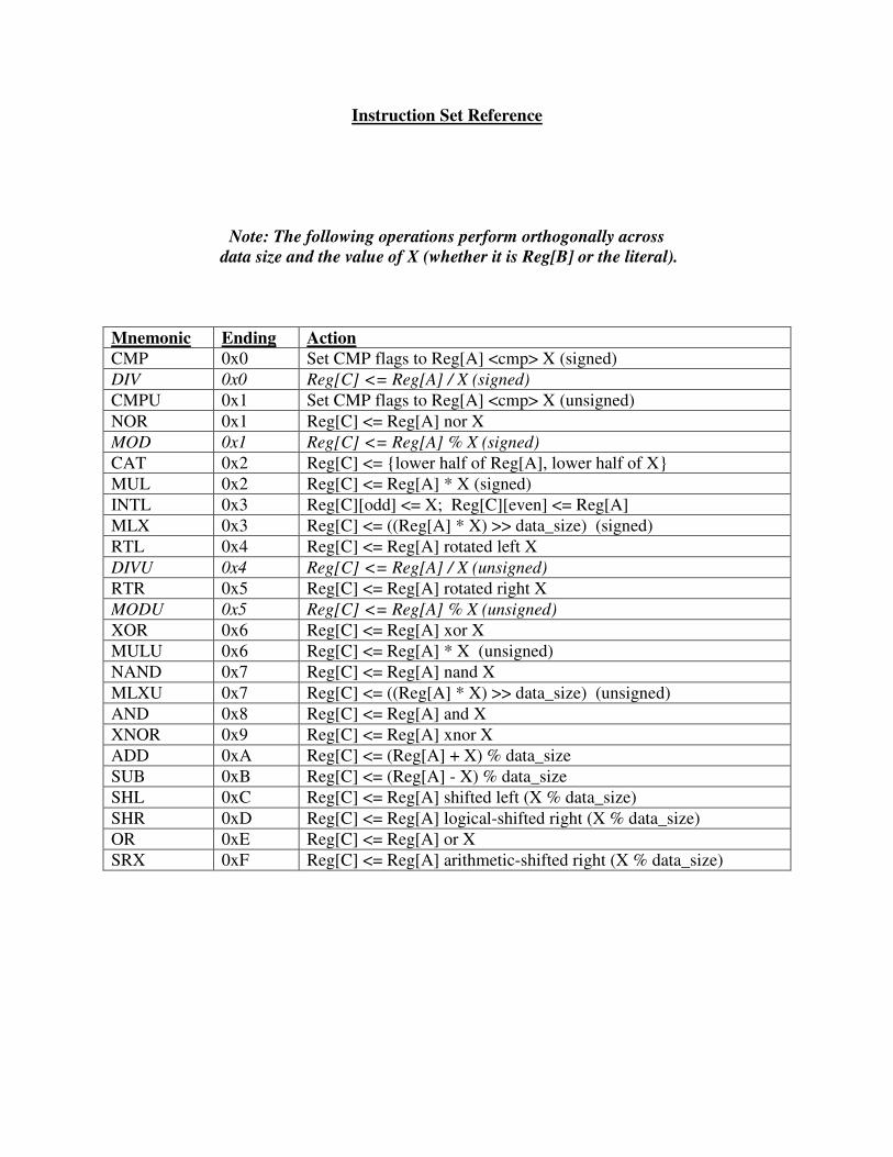
Note: The following operations perform orthogonally across
data size and the value of X (whether it is Reg[B] or the literal).
Mnemonic Ending Action
CMP 0x0 Set CMP flags to Reg[A] <cmp> X (signed)
DIV 0x0 Reg[C] <= Reg[A] / X (signed)
CMPU 0x1 Set CMP flags to Reg[A] <cmp> X (unsigned)
NOR 0x1 Reg[C] <= Reg[A] nor X
MOD 0x1 Reg[C] <= Reg[A] % X (signed)
CAT 0x2 Reg[C] <= {lower half of Reg[A], lower half of X}
MUL 0x2 Reg[C] <= Reg[A] * X (signed)
INTL 0x3 Reg[C][odd] <= X; Reg[C][even] <= Reg[A]
MLX 0x3 Reg[C] <= ((Reg[A] * X) >> data_size) (signed)
RTL 0x4 Reg[C] <= Reg[A] rotated left X
DIVU 0x4 Reg[C] <= Reg[A] / X (unsigned)
RTR 0x5 Reg[C] <= Reg[A] rotated right X
MODU 0x5 Reg[C] <= Reg[A] % X (unsigned)
XOR 0x6 Reg[C] <= Reg[A] xor X
MULU 0x6 Reg[C] <= Reg[A] * X (unsigned)
NAND 0x7 Reg[C] <= Reg[A] nand X
MLXU 0x7 Reg[C] <= ((Reg[A] * X) >> data_size) (unsigned)
AND 0x8 Reg[C] <= Reg[A] and X
XNOR 0x9 Reg[C] <= Reg[A] xnor X
ADD 0xA Reg[C] <= (Reg[A] + X) % data_size
SUB 0xB Reg[C] <= (Reg[A] - X) % data_size
SHL 0xC Reg[C] <= Reg[A] shifted left (X % data_size)
SHR 0xD Reg[C] <= Reg[A] logical-shifted right (X % data_size)
OR 0xE Reg[C] <= Reg[A] or X
SRX 0xF Reg[C] <= Reg[A] arithmetic-shifted right (X % data_size)
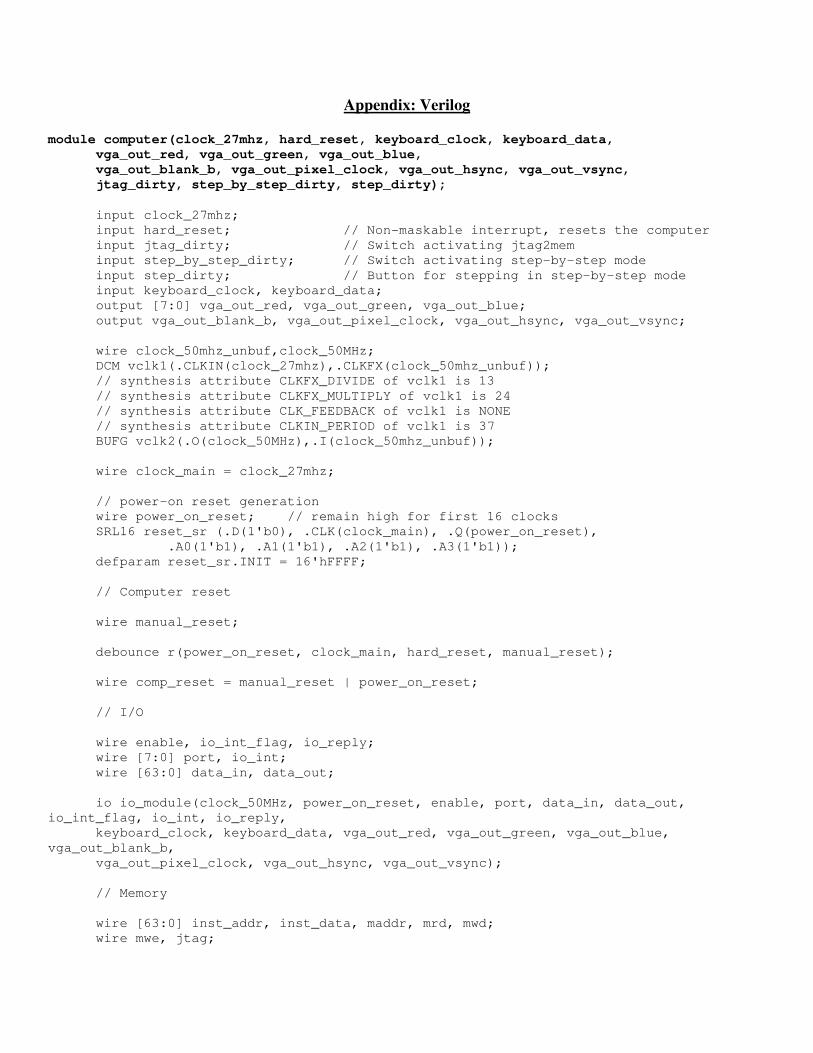
Appendix: Verilog
module computer(clock_27mhz, hard_reset, keyboard_clock, keyboard_data,
vga_out_red, vga_out_green, vga_out_blue,
vga_out_blank_b, vga_out_pixel_clock, vga_out_hsync, vga_out_vsync,
jtag_dirty, step_by_step_dirty, step_dirty);
input clock_27mhz;
input hard_reset; // Non-maskable interrupt, resets the computer
input jtag_dirty; // Switch activating jtag2mem
input step_by_step_dirty; // Switch activating step-by-step mode
input step_dirty; // Button for stepping in step-by-step mode
input keyboard_clock, keyboard_data;
output [7:0] vga_out_red, vga_out_green, vga_out_blue;
output vga_out_blank_b, vga_out_pixel_clock, vga_out_hsync, vga_out_vsync;
wire clock_50mhz_unbuf,clock_50MHz;
DCM vclk1(.CLKIN(clock_27mhz),.CLKFX(clock_50mhz_unbuf));
// synthesis attribute CLKFX_DIVIDE of vclk1 is 13
// synthesis attribute CLKFX_MULTIPLY of vclk1 is 24
// synthesis attribute CLK_FEEDBACK of vclk1 is NONE
// synthesis attribute CLKIN_PERIOD of vclk1 is 37
BUFG vclk2(.O(clock_50MHz),.I(clock_50mhz_unbuf));
wire clock_main = clock_27mhz;
// power-on reset generation
wire power_on_reset; // remain high for first 16 clocks
SRL16 reset_sr (.D(1'b0), .CLK(clock_main), .Q(power_on_reset),
.A0(1'b1), .A1(1'b1), .A2(1'b1), .A3(1'b1));
defparam reset_sr.INIT = 16'hFFFF;
// Computer reset
wire manual_reset;
debounce r(power_on_reset, clock_main, hard_reset, manual_reset);
wire comp_reset = manual_reset | power_on_reset;
// I/O
wire enable, io_int_flag, io_reply;
wire [7:0] port, io_int;
wire [63:0] data_in, data_out;
io io_module(clock_50MHz, power_on_reset, enable, port, data_in, data_out,
io_int_flag, io_int, io_reply,
keyboard_clock, keyboard_data, vga_out_red, vga_out_green, vga_out_blue,
vga_out_blank_b,
vga_out_pixel_clock, vga_out_hsync, vga_out_vsync);
// Memory
wire [63:0] inst_addr, inst_data, maddr, mrd, mwd;
wire mwe, jtag;
debounce j(power_on_reset, clock_main, jtag_dirty, jtag);
memory mem(clock_main, comp_reset, inst_addr[14:0], maddr[14:0], mwe, mwd,
inst_data, mrd, jtag);
// Stack
wire st_reset, st_overflow, st_underflow, st_enable, st_push;
wire [63:0] st_in, st_out;
stack s(clock_main, st_reset | comp_reset, st_overflow, st_underflow, st_enable,
st_push, st_in, st_out);
// Timer
wire set_time;
wire [63:0] new_time, time_msec;
timer t(clock_main, set_time, new_time, time_msec);
// RNG
wire [63:0] rand_data;
lfsr rng(clock_main, rand_data); // Linear Feedback Shift Register module
// CPU
wire step_by_step, step;
debounce sbs(power_on_reset, clock_main, step_by_step_dirty, step_by_step);
debounce st(power_on_reset, clock_main, step_dirty, step);
cpu proc(clock_main, comp_reset, enable, port, data_in, data_out, io_int_flag,
io_int,
io_reply, inst_addr, inst_data, mwe, maddr, mrd, mwd,
st_reset, st_overflow, st_underflow, st_enable, st_push, st_in, st_out,
set_time, new_time, time_msec, rand_data, step_by_step, step);
endmodule
module io(clock, reset, enable, port, data_in, data_out, io_int_send, io_int, io_reply,
kbd_clock, kbd_data,
vga_red, vga_green, vga_blue, vga_blank, vga_pixel_clock, vga_hsync, vga_vsync);
input clock, enable, reset;
output io_int_send; // Signal I/O interrupt
output io_reply; // Acknowledge I/O operation
input [7:0] port; // Location of I/O operation
output [7:0] io_int; // Location of I/O interrupt
input [63:0] data_in; // Data to devices
output [63:0] data_out; // Data to CPU
reg [63:0] data_out;

// Keyboard (PS/2)
input kbd_clock, kbd_data;
wire ascii_ready;
wire [7:0] ascii;
ps2_ascii_input keyboard(clock, reset, kbd_clock, kbd_data, ascii, ascii_ready);
// Monitor (640x480 VGA text-mode)
wire irq_60Hz;
output [7:0] vga_red, vga_green, vga_blue;
output vga_blank, vga_pixel_clock, vga_hsync, vga_vsync;
reg [63:0] disp_data;
reg irq_clear;
wire [31:0] disp_out;
wire [2:0] rgb;
assign vga_red = {8{rgb[2]}};
assign vga_green = {8{rgb[1]}};
assign vga_blue = {8{rgb[0]}};
wire blank;
assign vga_blank = ~blank;
vga monitor(clock, vga_hsync, vga_vsync, rgb, irq_60Hz, irq_clear,
enable & port[1], disp_data[41:32], disp_data[31:0], disp_out, blank,
vga_pixel_clock);
// Transmission
reg io_reply;
always @ (posedge clock) begin
if (enable) begin
// Bit 1 of the port signal writes data to the monitor
if (port[1]) begin
// Address in memory
disp_data[41:32] <= data_in[43:34];
// Access the desired byte
disp_data[31:0] <= data_in[33] ? (data_in[32] ? {data_in[7:0],
disp_out[23:0]}
: {disp_out[31:24],
data_in[23:16], disp_out[15:0]})
: (data_in[32] ? {disp_out[31:16],
data_in[15:8], disp_out[7:0]}
:
{disp_out[31:8], data_in[7:0]});
// Also send the contents of memory (before write)
data_out <= {32'b0, disp_out};
// VGA signal
irq_clear <= & data_in[43:34];

end
// Bit 0 of the port signal reads data from the keyboard
else if (port[0]) begin
data_out <= {56'b0, ascii};
end
// Acknowledge the operation
io_reply <= 1'b1;
end
else begin
// Acknowledge the end of the operation
io_reply <= 1'b0;
end
end
assign io_int_send = ascii_ready | irq_60Hz;
assign io_int[0] = ascii_ready;
assign io_int[1] = irq_60Hz;
endmodule
module memory(clock,reset,ia,ma,we,mwd,id,mrd,jtag);
input clock, reset;
input [14:0] ia;
input [14:0] ma;
input we;
input [63:0] mwd;
output [63:0] id;
output [63:0] mrd;
input jtag;
// jtag2mem interface to normal memory
wire [3:0] state;
wire [7:0] true_read_data;
wire [7:0] write_data;
wire [17:0] ram_addr;
wire ram_we;
jtag2mem #(.DBITS(8),.ABITS(18))
j2m(reset, clock, true_read_data, write_data, ram_addr, ram_we, state);
// Used to allow jtag2mem to operate on bytes, not words
assign true_read_data = ram_addr[2] ? (ram_addr[1] ? (ram_addr[0] ? mrd[7:0] :
mrd[15:8])
: (ram_addr[0] ? mrd[23:16] :
mrd[31:24]))
: (ram_addr[1] ? (ram_addr[0] ? mrd[39:32] :
mrd[47:40])
: (ram_addr[0] ? mrd[55:48] :
mrd[63:56]));
wire [63:0] true_write_data = ram_addr[2] ? (ram_addr[1] ? (ram_addr[0] ?
{mrd[63:8], write_data}
:
{mrd[63:16], write_data, mrd[7:0]})
: (ram_addr[0] ?
{mrd[63:24], write_data, mrd[15:0]}
:
{mrd[63:32], write_data, mrd[23:0]}))
: (ram_addr[1] ? (ram_addr[0] ?
{mrd[63:40], write_data, mrd[31:0]}
:
{mrd[63:48], write_data, mrd[39:0]})
: (ram_addr[0] ?
{mrd[63:56], write_data, mrd[47:0]}
:
{write_data, mrd[55:0]}));
// Actual memory (32768 64-bit words)
mem m(.addra(ia), .addrb(jtag ? ram_addr[17:3] : ma), .clka(clock), .clkb(clock),
.dinb(jtag ? true_write_data : mwd), .douta(id), .doutb(mrd), .web(jtag ? ram_we :
we));
endmodule
module stack(clock, reset, overflow, underflow, enable, push, in, out);
parameter WIDTH = 64;
parameter ADDRESS = 10;
parameter SIZE = 1024; // = 2 ** ADDRESS
input clock, reset;
output overflow, underflow;
input enable, push;
input [WIDTH-1:0] in;
output [WIDTH-1:0] out;
reg [ADDRESS-1:0] ptr; // Pointer to first unoccupied space in memory
reg overflow, underflow; // Stack exception cases
wire [ADDRESS-1:0] top = ptr - 1; // Pointer to top element of stack
// Shift the pointer for stack operations
always @ (posedge clock)
begin
// Reset the stack by dropping the pointer back to zero,
// removing access to every element that was in the stack
if (reset) begin
ptr <= 0;
overflow <= 1'b0;
underflow <= 1'b0;
end
// Stack enable means some operation will occur
else if (enable) begin
// Push operation increments ptr and possibly sets overflow
if (push) begin
ptr <= ptr + 1;
overflow <= overflow ? 1'b1 : (& ptr);
end
// Pop operation decrements ptr and possibly sets underflow
else begin
ptr <= ptr - 1;
underflow <= underflow ? 1'b1 : (~| ptr);
end
end
end
// Dual port memory for stack
stack_array mem(ptr, top, clock, clock, in, out, enable & push);
endmodule
module timer(clock, flush, new, msec);
parameter WIDTH = 64;
parameter TICKS_PER_MSEC = 27000;
input clock, flush;
input [WIDTH-1:0] new;
output [WIDTH-1:0] msec;
reg [15:0] count = 0; // enough to count to TICKS_PER_MSEC
reg [WIDTH-1:0] msec = 0; // current time in milliseconds
always @ (posedge clock) begin
// Set the user specified time
if (flush) begin
msec <= new;
count <= 0;
end
// Divide time into milliseconds
else if (count == TICKS_PER_MSEC) begin
msec <= msec + 1;
count <= 0;
end
else count <= count + 1;
end
endmodule

module cpu(clock, reset, io_enable, port, data_out, data_in, io_int_recv, io_int,
io_reply, inst_addr, inst_data, mwe, ma, mrd, mwd,
st_reset, st_overflow, st_underflow, st_enable, st_push, st_put, st_get,
set_time, new_time, time_msec, rand_data, step_by_step, step);
parameter WIDTH = 64;
parameter INT_ADDR = 8;
parameter NUM_INT = 256; // 2 ** INT_ADDR
parameter OP_SIZE = 8;
parameter REG_ADDR = 8;
parameter REG_BYTE_ADDR = 5;
parameter SXT_SIZE = 32;
input clock, reset;
// I/O
output io_enable;
output [7:0] port;
input [63:0] data_in;
output [63:0] data_out;
input [7:0] io_int;
input io_int_recv, io_reply;
// Memory
output [WIDTH - 1:0] inst_addr;
input [WIDTH - 1:0] inst_data;
output mwe;
output [WIDTH - 1:0] ma;
input [WIDTH - 1:0] mrd;
output [WIDTH - 1:0] mwd;
// Stack
output st_reset;
input st_overflow;
input st_underflow;
output st_enable;
output st_push;
output [WIDTH - 1:0] st_put;
input [WIDTH - 1:0] st_get;
// Timer
output set_time;
output [WIDTH - 1:0] new_time;
input [WIDTH - 1:0] time_msec;
// RNG
input [WIDTH - 1:0] rand_data;
// Microsequencer
wire enable, special;
wire [WIDTH - 1:0] ic;
wire cmp, word, cmp_signed;
wire [WIDTH - 1:0] a_word, b_word;
wire [7:0] a_byte, b_byte;
wire branch, call, jump;
wire [2:0] branch_cond;
wire [WIDTH - 1:0] bt, jt;
wire overflow, underflow, inst_stack_reset, inst_stack_pop, irq;
wire [INT_ADDR - 1:0] interrupt;
wire [6:1] cmp_flags;
wire irq_ack, irq_clear;
microsequencer ms(clock, reset, enable, ic, irq, interrupt, cmp_signed,
cmp, word, a_word, b_word, a_byte, b_byte, branch, call, jump, branch_cond, bt, jt,
overflow, underflow, inst_stack_reset, inst_stack_pop, special, irq_ack, irq_clear);
// Reg Manager
wire [REG_ADDR - 1:0] ra1_word, ra2_word;
wire [WIDTH - 1:0] rd1_word;
wire [WIDTH - 1:0] rd2_word;
wire we_word;
wire [REG_ADDR - 1:0] wa_word;
wire [WIDTH - 1:0] wd_word;
wire [REG_BYTE_ADDR - 1:0] ra1_byte, ra2_byte;
wire [7:0] rd1_byte, rd2_byte;
wire we_byte;
wire [REG_BYTE_ADDR - 1:0] wa_byte;
wire [7:0] wd_byte;
wire split_sig, join_sig, swap_sig;
reg_manager regfile(clock, ra1_word, ra2_word, rd1_word, rd2_word, we_word, wa_word,
wd_word, ra1_byte, ra2_byte, rd1_byte, rd2_byte, we_byte, wa_byte, wd_byte,
split_sig, join_sig, swap_sig);
// ALU
wire [3:0] func;
wire [WIDTH - 1:0] ans_word;
wire [7:0] ans_byte;
wire alu_overflow, alu_enable;
alu_manager alu(func, word, a_word, b_word, ans_word, a_byte, b_byte, ans_byte,
alu_overflow, alu_enable);
// Trap
wire trap_ret, div_by_zero, trap_enable;
wire [WIDTH - 1:0] trap_word;
wire [7:0] trap_byte;
wire [2:0] trap_op;
trap tr(clock, reset, trap_enable, trap_op, word, a_word, b_word, trap_word, a_byte,
b_byte, trap_byte, trap_ret, div_by_zero);
// System Timer
wire flush_period, systimer_int;

wire [WIDTH - 1:0] new_period, period;
sys_timer systimer(clock, reset, flush_period, new_period, period, systimer_int);
// Interrupt Handler
wire change_mask, set_mask, change_int_en, set_int_en;
wire [INT_ADDR - 1:0] int_val;
wire int_req, int_ack;
interrupt_handler ih(clock, reset, change_mask, set_mask, io_int, io_int_recv,
int_req, int_val,
alu_overflow, st_overflow, st_underflow, overflow, underflow, div_by_zero,
systimer_int,
int_ack, interrupt, irq, change_int_en, set_int_en, irq_ack, irq_clear);
// Control
input step_by_step, step;
wire b_sel, absolute, delay;
wire [3:0] wd_sel;
wire [7:0] operation = inst_data[WIDTH - 1:WIDTH - OP_SIZE];
wire [WIDTH - OP_SIZE - 1:0] good_data;
delayer d(clock, delay, reset, inst_data[WIDTH - OP_SIZE - 1:0], good_data[WIDTH -
OP_SIZE - 1:0]);
wire [REG_ADDR - 1:0]
addr1 = good_data[WIDTH - OP_SIZE - 1:WIDTH - OP_SIZE - REG_ADDR],
addr2 = good_data[WIDTH - OP_SIZE - REG_ADDR - 1:WIDTH - OP_SIZE - (2 *
REG_ADDR)],
addr3 = good_data[WIDTH - OP_SIZE - (2 * REG_ADDR) - 1:WIDTH - OP_SIZE - (3 *
REG_ADDR)];
wire [WIDTH - 1:0] sxt = {{(WIDTH - SXT_SIZE){good_data[SXT_SIZE - 1]}},
good_data[SXT_SIZE - 1:0]};
wire [INT_ADDR - 1:0] interrupt_constant = good_data[INT_ADDR - 1:0];
assign jt = rd1_word;
assign inst_addr = ic;
assign bt = ic + sxt;
assign port = good_data[7:0];
assign int_val = interrupt_constant;
assign int_table_addr = interrupt_constant;
assign ra1_word = addr2;
assign ra2_word = addr3;
assign wa_word = addr1;
assign ra1_byte = addr2[REG_BYTE_ADDR - 1:0];
assign ra2_byte = addr3[REG_BYTE_ADDR - 1:0];
assign wa_byte = addr1[REG_BYTE_ADDR - 1:0];
assign a_word = rd1_word;
assign b_word = b_sel ? sxt : rd2_word;
assign a_byte = rd1_byte;
assign b_byte = b_sel ? sxt[7:0] : rd2_byte;
assign mwd = rd1_word;
assign st_put = rd1_word;
assign new_time = rd1_word;
assign data_out = rd1_word;
assign int_vector_in = rd1_word;
assign new_period = rd1_word;
assign ma = absolute ? (rd2_word + sxt) : bt;
wdmux multi(wd_word, wd_sel, int_vector_out, ic, time_msec, period, rand_data,
st_get, data_in, mrd, trap_word, ans_word);
assign wd_byte = wd_sel[0] ? trap_byte : ans_byte;
control ctl(clock, reset, operation, io_enable, mwe, set_time, st_reset, st_enable,
st_push,
we_word, we_byte, split_sig, join_sig, func, word, swap_sig, b_sel, wd_sel,
absolute, irq,
trap_op, trap_ret, enable, change_mask, set_mask, change_int_en, set_int_en, cmp,
branch, call, jump,
branch_cond, inst_stack_reset, inst_stack_pop, int_req, int_ack, flush_period,
io_reply,
special, trap_enable, delay, alu_enable, step_by_step, step, cmp_signed);
endmodule
module wdmux(wd_word, wd_sel, int_vector_out, ic, time_msec, period, rand_data,
st_get, data_in, mrd, trap_word, ans_word);
parameter WIDTH = 64;
output [WIDTH-1:0] wd_word;
input [3:0] wd_sel;
input [WIDTH-1:0] int_vector_out, ic, time_msec, period, rand_data,
st_get, data_in, mrd, trap_word, ans_word;
assign wd_word = wd_sel[3] ? (wd_sel[2] ? ic
: (wd_sel[1] ? time_msec
: period))
: (wd_sel[2] ? (wd_sel[1] ? rand_data
: st_get)
: (wd_sel[1] ? (wd_sel[0] ? data_in
: mrd)
: (wd_sel[0] ? trap_word
:
ans_word)));
endmodule
module delayer(clock, delay, reset, signal, out);
parameter WIDTH = 56;
input clock, delay, reset;
input [WIDTH-1:0] signal;
output [WIDTH-1:0] out;
reg [WIDTH-1:0] delayed;
always @ (posedge clock) if (~delay | reset) delayed <= signal;
assign out = delay ? delayed : signal;
endmodule
module microsequencer(clock, reset, enable, ic, irq, interrupt, cmp_signed,
cmp, word, aword, bword, abyte, bbyte, branch, call, jump, branch_cond, bt, jt,
overflow, underflow, inst_stack_reset, inst_stack_pop, special, irq_ack, irq_clear);
parameter WIDTH = 64;
parameter INT_ADDR = 8;
parameter NUM_INT = 256; // 2 ** INT_ADDR
input clock, reset, enable;
output [WIDTH - 1:0] ic;
output special;
// Interrupt
input irq; // Interrupt request
output irq_ack; // Acknowledge the irq
input irq_clear; // Acknowledge the irq_ack
input [INT_ADDR - 1:0] interrupt; // Number of interrupt requested
// Compare
input cmp, word, cmp_signed;
input [WIDTH - 1:0] aword, bword;
input [7:0] abyte, bbyte;
wire [6:1] cmp_w_res, cmp_b_res;
reg [6:1] cmp_flags = 0;
compare cmp_w(aword, bword, cmp_signed, cmp_w_res);
compare cmp_b(abyte, bbyte, cmp_signed, cmp_b_res);
defparam cmp_b.WIDTH = 8;
always @ (posedge clock) if (cmp) cmp_flags[6:1] <= word ? cmp_w_res : cmp_b_res;
// Branch
input branch, jump, call;
input [2:0] branch_cond;
input [WIDTH - 1:0] bt, jt;
// Stack (instruction)
output overflow, underflow;
input inst_stack_reset, inst_stack_pop;

wire [WIDTH - 1:0] inst_stack_out;
wire [WIDTH - 1:0] icpp = ic + 1;
// Push instruction counter when we can return
// (either from a call or an interrupt)
wire push = irq | call;
stack s(clock, inst_stack_reset | reset, overflow, underflow,
push ^ inst_stack_pop, push, icpp, inst_stack_out);
// IC Calculation
// Note that cmp_flags[7] = 1'b1 and cmp_flags[0] = 1'b0
// This allows branch_cond[7] to be unconditional branch
// and branch_cond[0] to be never branch (no operation)
ic_calc calc(clock, reset, ic, enable, push, inst_stack_pop, jump, branch, {1'b1,
cmp_flags, 1'b0},
branch_cond, irq, interrupt, inst_stack_out, jt, bt, icpp, special, irq_ack,
irq_clear);
endmodule
module ic_calc(clock, reset, ic, enable, push, inst_stack_pop, jump, branch,
cmp_flags, branch_cond, irq, interrupt, inst_stack_out, jt, bt, icpp, special,
irq_ack, irq_clear);
parameter WIDTH = 64;
parameter INT_ADDR = 8;
parameter NUM_INT = 256; // 2 ** INT_ADDR
input clock, reset, irq_clear;
output [WIDTH - 1:0] ic;
reg [WIDTH - 1:0] ic;
input enable, push, inst_stack_pop, jump, branch, irq;
input [INT_ADDR - 1:0] interrupt;
input [7:0] cmp_flags;
input [2:0] branch_cond;
input [WIDTH - 1:0] inst_stack_out, jt, bt, icpp;
output special, irq_ack; // special is a signal that ic is not becoming ic + 1
reg special, irq_ack; // irq_ack is a signal that the irq has been seen and
jumped to
always @ (posedge clock) begin
// Reset clears special
if (reset) begin
ic <= NUM_INT; // First NUM_INT words of memory are reserved for
interrupts
irq_ack <= 1'b0;
special <= 1'b1;
end
// Irq_clear acknowledges the acknowledge
else if (irq_clear) begin
irq_ack <= 1'b0;
end

// Irq requires a jump to the proper place
else if (irq) begin
ic <= interrupt; // First NUM_INT words of memory are reserved for
interrupts
irq_ack <= 1'b1;
special <= 1'b1;
end
else if (enable) begin
// Call or jump was requested
if (push) begin
ic <= jump ? jt : bt;
special <= 1'b1;
end
// Return or return from interrupt was requested
else if (inst_stack_pop) begin
ic <= inst_stack_out;
special <= 1'b1;
end
// Branch was requested (conditional execution)
else if (branch & cmp_flags[branch_cond]) begin
ic <= bt;
special <= 1'b1;
end
// Nothing special happened
else begin
ic <= icpp;
special <= 1'b0;
end
end
// Special is a one cycle signal
else if (special) special <= 1'b0;
end
endmodule
module compare(a, b, sign, result);
parameter WIDTH = 64;
// Signals used as branch conditions
// (bit 0 is equal, bit 1 is less than, bit 2 is greater than;
// each code is the union of its components)
// 3'b000 should always be low, 3'b111 should always be high
parameter EQ = 3'b001;
parameter LT = 3'b010;
parameter LE = 3'b011;
parameter GT = 3'b100;
parameter GE = 3'b101;
parameter NE = 3'b110;

input [WIDTH - 1:0] a, b;
input sign;
output [6:1] result;
// Handle signedness
wire [WIDTH - 1:0] new_a, new_b;
assign new_a = {sign ^ a[WIDTH - 1], a[WIDTH - 2:0]};
assign new_b = {sign ^ b[WIDTH - 1], b[WIDTH - 2:0]};
assign result[NE] = |(a ^ b);
assign result[EQ] = ~result[NE];
assign result[LT] = new_a < new_b;
assign result[GE] = ~result[LT];
assign result[LE] = result[EQ] | result[LT];
assign result[GT] = ~(result[EQ] | result[LT]);
endmodule
module reg_manager(clock,ra1_word,ra2_word,rd1_word,rd2_word,we_word,wa_word,
wd_word,ra1_byte,ra2_byte,rd1_byte,rd2_byte,we_byte,
wa_byte,wd_byte,split_sig,join_sig,swap_sig);
parameter WIDTH = 64;
parameter ADDR_WORD = 8;
parameter SIZE_WORD = 256; // 2 ** ADDR_WORD
parameter ZERO_WORD = SIZE_WORD - 1;
parameter ADDR_BYTE = 5;
parameter SIZE_BYTE = 32; // 2 ** ADDR_BYTE
parameter ZERO_BYTE = SIZE_BYTE - 1;
input clock;
input [ADDR_WORD - 1:0] ra1_word;
input [ADDR_WORD - 1:0] ra2_word;
output [WIDTH - 1:0] rd1_word;
output [WIDTH - 1:0] rd2_word;
input we_word;
input [ADDR_WORD - 1:0] wa_word;
input [WIDTH - 1:0] wd_word;
input [ADDR_BYTE - 1:0] ra1_byte;
input [ADDR_BYTE - 1:0] ra2_byte;
output [7:0] rd1_byte;
output [7:0] rd2_byte;
input we_byte;
input [ADDR_BYTE - 1:0] wa_byte;
input [7:0] wd_byte;
input split_sig;
input join_sig;
input swap_sig;
wire [WIDTH - 1:0] gout;
regfile_byte reg_b(clock, split_sig, swap_sig, rd1_word, gout,
ra1_byte, ra2_byte, rd1_byte, rd2_byte, we_byte, wa_byte, wd_byte);
defparam reg_b.SIZE = SIZE_BYTE;
defparam reg_b.ADDRESS = ADDR_BYTE;
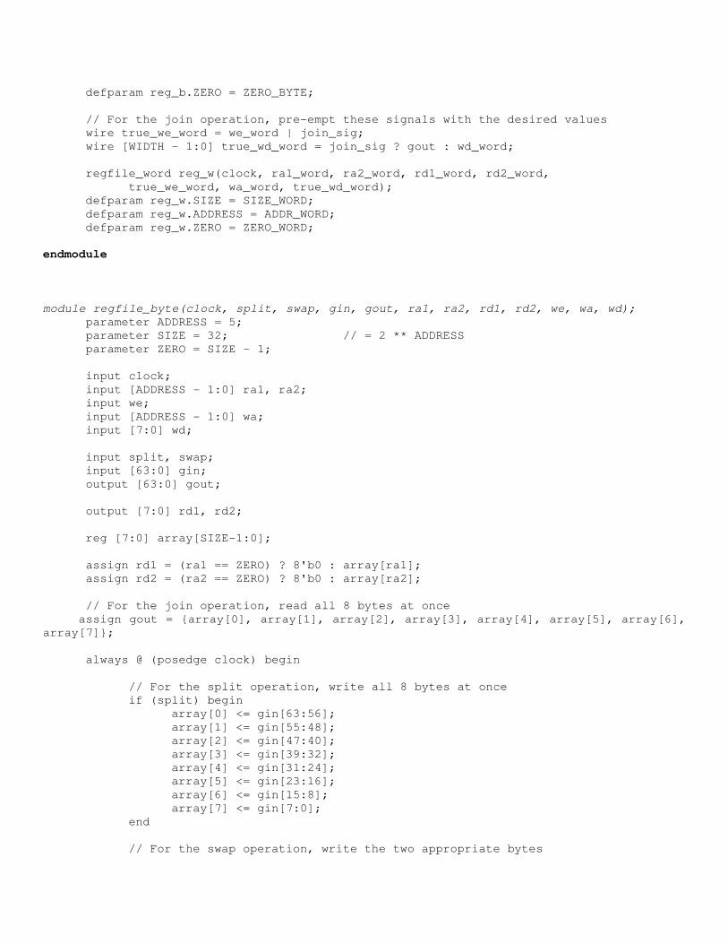
defparam reg_b.ZERO = ZERO_BYTE;
// For the join operation, pre-empt these signals with the desired values
wire true_we_word = we_word | join_sig;
wire [WIDTH - 1:0] true_wd_word = join_sig ? gout : wd_word;
regfile_word reg_w(clock, ra1_word, ra2_word, rd1_word, rd2_word,
true_we_word, wa_word, true_wd_word);
defparam reg_w.SIZE = SIZE_WORD;
defparam reg_w.ADDRESS = ADDR_WORD;
defparam reg_w.ZERO = ZERO_WORD;
endmodule
module regfile_byte(clock, split, swap, gin, gout, ra1, ra2, rd1, rd2, we, wa, wd);
parameter ADDRESS = 5;
parameter SIZE = 32; // = 2 ** ADDRESS
parameter ZERO = SIZE - 1;
input clock;
input [ADDRESS - 1:0] ra1, ra2;
input we;
input [ADDRESS - 1:0] wa;
input [7:0] wd;
input split, swap;
input [63:0] gin;
output [63:0] gout;
output [7:0] rd1, rd2;
reg [7:0] array[SIZE-1:0];
assign rd1 = (ra1 == ZERO) ? 8'b0 : array[ra1];
assign rd2 = (ra2 == ZERO) ? 8'b0 : array[ra2];
// For the join operation, read all 8 bytes at once
assign gout = {array[0], array[1], array[2], array[3], array[4], array[5], array[6],
array[7]};
always @ (posedge clock) begin
// For the split operation, write all 8 bytes at once
if (split) begin
array[0] <= gin[63:56];
array[1] <= gin[55:48];
array[2] <= gin[47:40];
array[3] <= gin[39:32];
array[4] <= gin[31:24];
array[5] <= gin[23:16];
array[6] <= gin[15:8];
array[7] <= gin[7:0];
end
// For the swap operation, write the two appropriate bytes
else if (swap) begin
array[ra1] <= rd2;
array[ra2] <= rd1;
end
// Perform normal write operation
else if (we) array[wa] <= wd;
end
endmodule
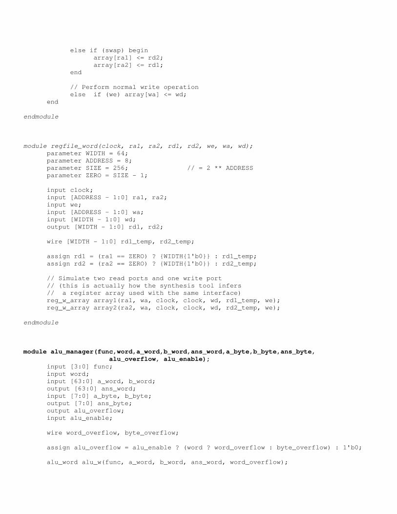
module regfile_word(clock, ra1, ra2, rd1, rd2, we, wa, wd);
parameter WIDTH = 64;
parameter ADDRESS = 8;
parameter SIZE = 256; // = 2 ** ADDRESS
parameter ZERO = SIZE - 1;
input clock;
input [ADDRESS - 1:0] ra1, ra2;
input we;
input [ADDRESS - 1:0] wa;
input [WIDTH - 1:0] wd;
output [WIDTH - 1:0] rd1, rd2;
wire [WIDTH - 1:0] rd1_temp, rd2_temp;
assign rd1 = (ra1 == ZERO) ? {WIDTH{1'b0}} : rd1_temp;
assign rd2 = (ra2 == ZERO) ? {WIDTH{1'b0}} : rd2_temp;
// Simulate two read ports and one write port
// (this is actually how the synthesis tool infers
// a register array used with the same interface)
reg_w_array array1(ra1, wa, clock, clock, wd, rd1_temp, we);
reg_w_array array2(ra2, wa, clock, clock, wd, rd2_temp, we);
endmodule
module alu_manager(func,word,a_word,b_word,ans_word,a_byte,b_byte,ans_byte,
alu_overflow, alu_enable);
input [3:0] func;
input word;
input [63:0] a_word, b_word;
output [63:0] ans_word;
input [7:0] a_byte, b_byte;
output [7:0] ans_byte;
output alu_overflow;
input alu_enable;
wire word_overflow, byte_overflow;
assign alu_overflow = alu_enable ? (word ? word_overflow : byte_overflow) : 1'b0;
alu_word alu_w(func, a_word, b_word, ans_word, word_overflow);
alu_byte alu_b(func, a_byte, b_byte, ans_byte, byte_overflow);
endmodule
module alu_word(func, a, b, answer, overflow);
///////////////////
// ALU Functions //
///////////////////
// Notice the Boolean codes are special
// Bit (2*x + y) is (x OP y)
parameter REV = 4'b0000;
parameter NOR = 4'b0001;
parameter CAT = 4'b0010;
parameter INTL = 4'b0011;
parameter RTL = 4'b0100;
parameter RTR = 4'b0101;
parameter XOR = 4'b0110;
parameter NAND = 4'b0111;
parameter AND = 4'b1000;
parameter XNOR = 4'b1001;
parameter ADD = 4'b1010;
parameter SUB = 4'b1011;
parameter SHL = 4'b1100;
parameter SHR = 4'b1101;
parameter OR = 4'b1110;
parameter SRX = 4'b1111;
input [3:0] func;
input [63:0] a, b;
output [63:0] answer;
output overflow;
wire use_adder = (func[3:1] == 3'b101);
wire use_bool = (func[2] == func[1]) & ((func[3] ^ func[2]) ^ (func[1] ^ func[0]));
wire use_twiddle = (func[3:1] == 3'b001) | (func == REV);
wire [63:0] adder_val, shift_val, bool_val, twiddle_val;
add addition(a, b, func[0], overflow, ~func[0], adder_val); // 64-bit adder-
subtracter module
shift_word s((a[63] & func[1]), func[3], func[0], a, b[5:0], shift_val);
bool bo(func, a, b, bool_val);
twiddle_word t(func[1], func[0], a, b[31:0], twiddle_val);
wire [63:0] first = use_adder ? adder_val : shift_val;
wire [63:0] second = use_bool ? bool_val : first;
assign answer = use_twiddle ? twiddle_val : second;
endmodule
module alu_byte(func, a, b, answer, overflow);
///////////////////
// ALU Functions //
///////////////////
// Notice the Boolean codes are special
// Bit (2*x + y) is (x OP y)
parameter REV = 4'b0000;
parameter NOR = 4'b0001;
parameter CAT = 4'b0010;
parameter INTL = 4'b0011;
parameter RTL = 4'b0100;
parameter RTR = 4'b0101;
parameter XOR = 4'b0110;
parameter NAND = 4'b0111;
parameter AND = 4'b1000;
parameter XNOR = 4'b1001;
parameter ADD = 4'b1010;
parameter SUB = 4'b1011;
parameter SHL = 4'b1100;
parameter SHR = 4'b1101;
parameter OR = 4'b1110;
parameter SRX = 4'b1111;
input [3:0] func;
input [7:0] a, b;
output [7:0] answer;
output overflow;
wire use_adder = (func[3:1] == 3'b101);
wire use_bool = (func[2] == func[1]) & ((func[3] ^ func[2]) ^ (func[1] ^ func[0]));
wire use_twiddle = (func[3:1] == 3'b001) | (func == REV);
wire [7:0] adder_val, shift_val, bool_val, twiddle_val;
add_byte add(a, b, func[0], overflow, ~func[0], adder_val); // 8-bit adder-
subtracter module
shift_byte s((a[7] & func[1]), func[3], func[0], a, b[2:0], shift_val);
bool bo(func, a, b, bool_val);
defparam bo.WIDTH = 8;
twiddle_byte t(func[1], func[0], a, b[3:0], twiddle_val);
wire [7:0] first = use_adder ? adder_val : shift_val;
wire [7:0] second = use_bool ? bool_val : first;
assign answer = use_twiddle ? twiddle_val : second;
endmodule
module bool(func, a, b, answer);
parameter WIDTH = 64;
input [3:0] func;
input [WIDTH - 1:0] a, b;
output [WIDTH - 1:0] answer;

// This mux, with the values of each Boolean operation,
// performs the requested function
mux4 m[WIDTH - 1:0] (answer[WIDTH - 1:0], a, b, func);
endmodule
module mux4(out, bit1, bit0, values);
output out;
input bit1, bit0;
input [3:0] values;
assign out = values[{bit1, bit0}];
endmodule
module shift_word(sign, op, dir, a, b, answer);
input sign, op, dir;
input [63:0] a;
input [5:0] b;
output [63:0] answer;
// Selecting a certain consecutive 64 bits of this array
// gives all possible rotations and shifts
wire [255:0] shifter;
assign shifter = {{64{sign}}, a, a, 64'b0};
// Figure out the value of the start of those bits
wire [7:0] base;
assign base = (op ^ dir) ? (dir ? 64 + b : 64 - b) :
(dir ? 128 + b : 128 - b);
// Select the bits
wire [190:0] lev1;
assign lev1 = base[7] ? {63'b0, shifter[255:128]} : shifter[190:0];
wire [126:0] lev2;
assign lev2 = base[6] ? lev1[190:64] : lev1[126:0];
wire [94:0] lev3;
assign lev3 = base[5] ? lev2[126:32] : lev2[94:0];
wire [78:0] lev4;
assign lev4 = base[4] ? lev3[94:16] : lev3[78:0];
wire [70:0] lev5;
assign lev5 = base[3] ? lev4[78:8] : lev4[70:0];
wire [66:0] lev6;
assign lev6 = base[2] ? lev5[70:4] : lev5[66:0];
wire [64:0] lev7;
assign lev7 = base[1] ? lev6[66:2] : lev6[64:0];
assign answer = base[0] ? lev7[64:1] : lev7[63:0];
endmodule

module shift_byte(sign, op, dir, a, b, answer);
input sign, op, dir;
input [7:0] a;
input [2:0] b;
output [7:0] answer;
// Selecting a certain consecutive 8 bits of this array
// gives all possible rotations and shifts
wire [31:0] shifter;
assign shifter = {{8{sign}}, a, a, 8'b0};
// Figure out the value of the start of those bits
wire [4:0] base;
assign base = (op ^ dir) ? (dir ? 8 + b : 8 - b) :
(dir ? 16 + b : 16 - b);
// Select the bits
wire [22:0] lev1;
assign lev1 = base[4] ? {7'b0, shifter[31:16]} : shifter[22:0];
wire [14:0] lev2;
assign lev2 = base[3] ? lev1[22:8] : lev1[14:0];
wire [10:0] lev3;
assign lev3 = base[2] ? lev2[14:4] : lev2[10:0];
wire [8:0] lev4;
assign lev4 = base[1] ? lev3[10:2] : lev3[8:0];
assign answer = base[0] ? lev4[8:1] : lev4[7:0];
endmodule
module twiddle_word(two_op, interleave, a_word, b_half_word, ans_word);
input two_op, interleave;
input [63:0] a_word;
input [31:0] b_half_word;
output [63:0] ans_word;
assign ans_word = two_op ? (interleave ? {
// Interleave
// lower half of b goes to odds
// lower half of a goes to evens
b_half_word[31], a_word[31], b_half_word[30], a_word[30],
b_half_word[29], a_word[29], b_half_word[28], a_word[28],
b_half_word[27], a_word[27], b_half_word[26], a_word[26],
b_half_word[25], a_word[25], b_half_word[24], a_word[24],
b_half_word[23], a_word[23], b_half_word[22], a_word[22],
b_half_word[21], a_word[21], b_half_word[20], a_word[20],
b_half_word[19], a_word[19], b_half_word[18], a_word[18],
b_half_word[17], a_word[17], b_half_word[16], a_word[16],
b_half_word[15], a_word[15], b_half_word[14], a_word[14],
b_half_word[13], a_word[13], b_half_word[12], a_word[12],
b_half_word[11], a_word[11], b_half_word[10], a_word[10],
b_half_word[9], a_word[9], b_half_word[8], a_word[8],

b_half_word[7], a_word[7], b_half_word[6], a_word[6],
b_half_word[5], a_word[5], b_half_word[4], a_word[4],
b_half_word[3], a_word[3], b_half_word[2], a_word[2],
b_half_word[1], a_word[1], b_half_word[0], a_word[0]} :
// Concatenate lower halves of a and b
{a_word[31:0], b_half_word}) : {
// Reverse a
a_word[0], a_word[1], a_word[2], a_word[3],
a_word[4], a_word[5], a_word[6], a_word[7],
a_word[8], a_word[9], a_word[10], a_word[11],
a_word[12], a_word[13], a_word[14], a_word[15],
a_word[16], a_word[17], a_word[18], a_word[19],
a_word[20], a_word[21], a_word[22], a_word[23],
a_word[24], a_word[25], a_word[26], a_word[27],
a_word[28], a_word[29], a_word[30], a_word[31],
a_word[32], a_word[33], a_word[34], a_word[35],
a_word[36], a_word[37], a_word[38], a_word[39],
a_word[40], a_word[41], a_word[42], a_word[43],
a_word[44], a_word[45], a_word[46], a_word[47],
a_word[48], a_word[49], a_word[50], a_word[51],
a_word[52], a_word[53], a_word[54], a_word[55],
a_word[56], a_word[57], a_word[58], a_word[59],
a_word[60], a_word[61], a_word[62], a_word[63]};
endmodule
module twiddle_byte(two_op, interleave, a_byte, b_nibble, ans_byte);
input two_op, interleave;
input [7:0] a_byte;
input [3:0] b_nibble;
output [7:0] ans_byte;
assign ans_byte = two_op ? (interleave ? {
// Interleave
// lower half of b goes to odds
// lower half of a goes to evens
b_nibble[3], a_byte[3], b_nibble[2], a_byte[2],
b_nibble[1], a_byte[1], b_nibble[0], a_byte[0]} :
// Concatenate lower halves of a and b
{a_byte[3:0], b_nibble}) : {
// Reverse a
a_byte[0], a_byte[1], a_byte[2], a_byte[3],
a_byte[4], a_byte[5], a_byte[6], a_byte[7]};
endmodule
module trap(clock, reset, enable, operation, alu_word_sig, a_word, b_word, trap_word,
a_byte, b_byte, trap_byte, trap_ret, div_by_zero);
parameter WIDTH = 64;
// Trap functions
parameter MUL = 4'h0;
parameter MLX = 4'h1;
parameter DIV = 4'h2;
parameter MOD = 4'h3;
parameter MULU = 4'h4;
parameter MLXU = 4'h5;
parameter DIVU = 4'h6;
parameter MODU = 4'h7;
input clock, reset, enable;
input [2:0] operation;
input alu_word_sig;
input [WIDTH - 1:0] a_word, b_word;
output [WIDTH - 1:0] trap_word;
input [7:0] a_byte, b_byte;
output [7:0] trap_byte;
output trap_ret; // Trap return from computation signal
output div_by_zero; // Divide by zero interrupt
reg [WIDTH - 1:0] trap_word;
reg [7:0] trap_byte;
reg trap_ret;
// Pulse the enable signal to know when to start computation
reg old_enable;
always @ (posedge clock) old_enable <= reset ? 0 : enable;
wire en_pulse = enable & ~old_enable;
// Delay that pulse to wait for the data to show up from regfile
reg en_after_pulse;
always @ (posedge clock) begin
if (en_pulse) en_after_pulse <= 1'b1;
else if (en_after_pulse) en_after_pulse <= 1'b0;
end
// Hold on to the operation being executed to know which value to return
reg [3:0] last;
always @ (posedge clock) if (~enable | en_pulse) last <= {alu_word_sig, operation};
wire word = last[3];
wire uns = last[2];
wire mul_op = last[1];
wire special = last[0];
parameter OP_DIVB = 3'b000;
parameter OP_DIVW = 3'b001;
parameter OP_MULB = 3'b010;
parameter OP_MULW = 3'b011;

parameter OP_DIVBU = 3'b100;
parameter OP_DIVWU = 3'b101;
parameter OP_MULBU = 3'b110;
parameter OP_MULWU = 3'b111;
parameter AR_DIV = 2'b00;
parameter AR_MUL = 2'b01;
parameter AR_DIVU = 2'b10;
parameter AR_MULU = 2'b11;
// Multiplex the modules from start to finish
wire [7:0] decode = {8{enable}} & (uns ? (mul_op ? (word ? 128 : 64)
: (word ? 32 : 16))
: (mul_op ? (word ? 8 : 4)
: (word ? 2 : 1)));
wire [7:0] return;
wire [WIDTH - 1:0] std_word[3:0];
wire [WIDTH - 1:0] alt_word[3:0];
wire [7:0] std_byte[3:0];
wire [7:0] alt_byte[3:0];
///// All modules pipelined
///// multiply: 1 cycle / 8 bits
///// divide : 1 cycle / 4 bits
// 64-bit signed multiplier (all 128 bits of output used)
multiply mul_w(clock, a_word, b_word, {alt_word[AR_MUL], std_word[AR_MUL]},
decode[OP_MULW], reset, en_after_pulse, return[OP_MULW]);
// 8-bit signed multiplier (all 16 bits of output used)
mul_byte mul_b(clock, a_byte, b_byte, {alt_byte[AR_MUL], std_byte[AR_MUL]},
decode[OP_MULB], reset, en_after_pulse, return[OP_MULB]);
// 64-bit unsigned multiplier (all 128 bits of output used)
multiply_uns mul_w_u(clock, a_word, b_word, {alt_word[AR_MULU], std_word[AR_MULU]},
decode[OP_MULWU], reset, en_after_pulse, return[OP_MULWU]);
// 8-bit unsigned multiplier (all 16 bits of output used)
mul_byte_uns mul_b_u(clock, a_byte, b_byte, {alt_byte[AR_MULU], std_byte[AR_MULU]},
decode[OP_MULBU], reset, en_after_pulse, return[OP_MULBU]);
// Quickly realize the divide by zero condition
assign div_by_zero = ~en_pulse & (((decode[OP_DIVW] | decode[OP_DIVWU]) & (~|
b_word[31:0])) |
((decode[OP_DIVB] | decode[OP_DIVBU]) & (~|
b_byte)));
// Note: no dividers were included in the demonstration design
// There were problems with implementing them on the labkit
/*
wire [31:0] quot_w, rem_w;
divide div_w(a_word[31:0], b_word[31:0], quot_w, rem_w,
clock, return[OP_DIVW], div_by_zero, reset, decode[OP_DIVW]);
assign std_word[AR_DIV] = {{(WIDTH - 32){quot_w[31]}}, quot_w};
assign alt_word[AR_DIV] = {{(WIDTH - 32){rem_w[31]}}, rem_w};
div_byte div_b(a_byte, b_byte, std_byte[AR_DIV], alt_byte[AR_DIV],
clock, return[OP_DIVB], div_by_zero, reset, decode[OP_DIVB]);
wire [31:0] quot_w_u, rem_w_u;
divide_uns div_w_u(a_word[31:0], b_word[31:0], quot_w_u, rem_w_u,
clock, return[OP_DIVWU], div_by_zero, reset, decode[OP_DIVWU]);
assign std_word[AR_DIVU] = {{(WIDTH - 32){quot_w[31]}}, quot_w_u};
assign alt_word[AR_DIVU] = {{(WIDTH - 32){rem_w[31]}}, rem_w_u};
div_byte_uns div_b_u(a_byte, b_byte, std_byte[AR_DIVU], alt_byte[AR_DIVU],
clock, return[OP_DIVBU], div_by_zero, reset, decode[OP_DIVBU]);
*/
always @ (posedge clock) begin
if (reset) trap_ret <= 1'b0;
// Stop computing on divide by zero
else if (div_by_zero) trap_ret <= 1'b1;
// Stop computing when the desired module is finished
// Set the appropriate output value
else if (| (decode & return)) begin
trap_ret <= 1'b1;
trap_byte <= special ? (uns ? (mul_op ? alt_byte[AR_MULU]
: alt_byte[AR_DIVU])
: (mul_op ? alt_byte[AR_MUL]
: alt_byte[AR_DIV]))
: (uns ? (mul_op ? std_byte[AR_MULU]
: std_byte[AR_DIVU])
: (mul_op ? std_byte[AR_MUL]
: std_byte[AR_DIV]));
trap_word <= special ? (uns ? (mul_op ? alt_word[AR_MULU]
: alt_word[AR_DIVU])
: (mul_op ? alt_word[AR_MUL]
: alt_word[AR_DIV]))
: (uns ? (mul_op ? std_word[AR_MULU]
: std_word[AR_DIVU])
: (mul_op ? std_word[AR_MUL]
: std_word[AR_DIV]));
end
// trap_ret is a one-cycle signal
if (trap_ret) trap_ret <= 1'b0;
end
endmodule
module sys_timer(clock, reset, flush, new_period, period, signal);
parameter WIDTH = 64;
parameter TICKS_PER_USEC = 27;
input clock, reset, flush;
input [WIDTH - 1:0] new_period;
output [WIDTH - 1:0] period;
output signal;

reg signal;
reg [4:0] ctr = 0; // enough to count to TICKS_PER_USEC
reg [WIDTH - 1:0] count = 0;
reg [WIDTH - 1:0] period = 0; // Period of system timer interrupts, in
microseconds
always @ (posedge clock) begin
// Reset everything and set the period to one second
if (reset) begin
ctr <= 0;
count <= 0;
period <= 1000000;
signal <= 1'b0;
end
// Set the period to the user-specified value and reset everything else
else if (flush) begin
ctr <= 0;
count <= 0;
period <= new_period;
signal <= 1'b0;
end
// Divide time into microseconds
else if (ctr == TICKS_PER_USEC) begin
count <= count + 1;
ctr <= 0;
end
// System timer signal
else if (count == period) begin
signal <= 1'b1;
count <= 0;
end
// System timer signal lasts one cycle
else begin
ctr <= ctr + 1;
signal <= 1'b0;
end
end
endmodule
module interrupt_handler(clock, reset, change_mask, set_mask, io_int, io_int_recv,
int_req, int_val, alu_overflow, st_overflow, st_underflow, overflow, underflow,
div_by_zero, systimer_int, int_ack, interrupt, irq, change_enable, set_enable,
irq_ack, irq_clear);
parameter INT_ADDR = 8;
parameter NUM_INT = 256; // 2 ** INT_ADDR
parameter SYS_TIMER = 0;
parameter KEYBOARD = 1;
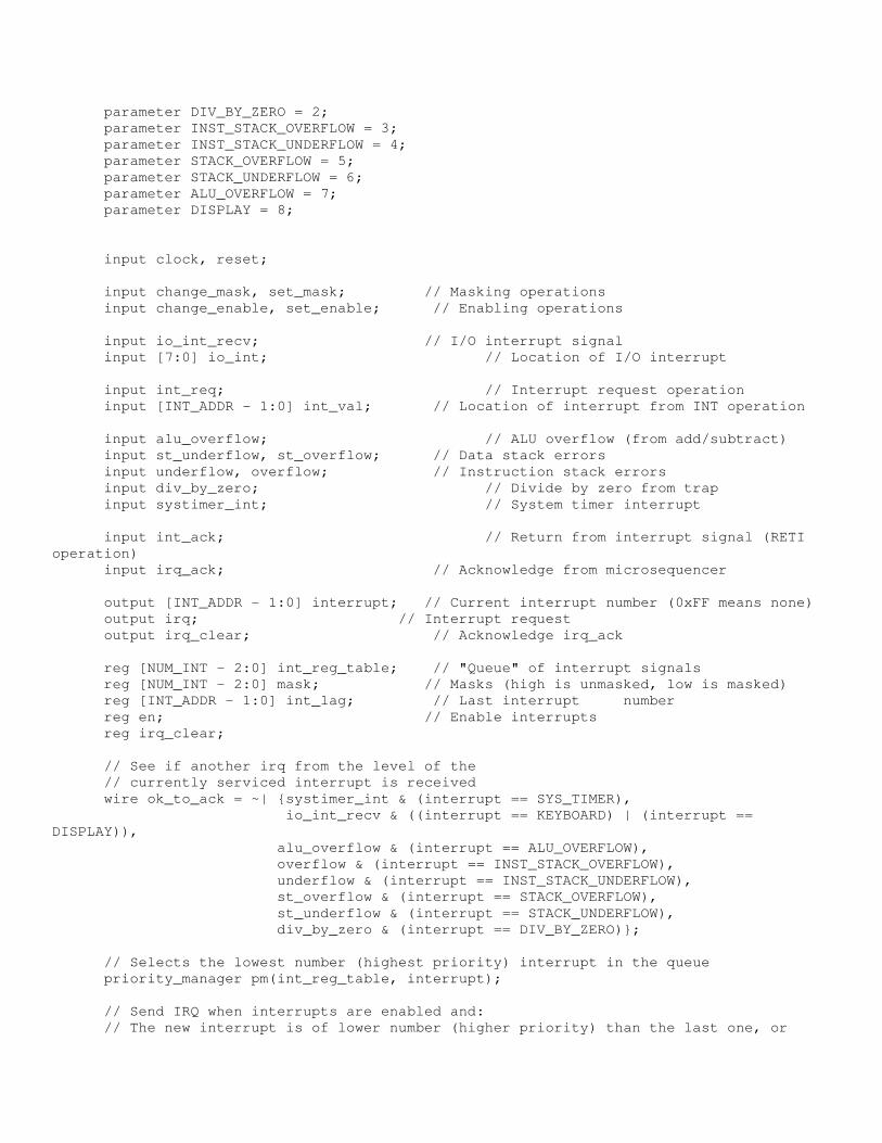
parameter DIV_BY_ZERO = 2;
parameter INST_STACK_OVERFLOW = 3;
parameter INST_STACK_UNDERFLOW = 4;
parameter STACK_OVERFLOW = 5;
parameter STACK_UNDERFLOW = 6;
parameter ALU_OVERFLOW = 7;
parameter DISPLAY = 8;
input clock, reset;
input change_mask, set_mask; // Masking operations
input change_enable, set_enable; // Enabling operations
input io_int_recv; // I/O interrupt signal
input [7:0] io_int; // Location of I/O interrupt
input int_req; // Interrupt request operation
input [INT_ADDR - 1:0] int_val; // Location of interrupt from INT operation
input alu_overflow; // ALU overflow (from add/subtract)
input st_underflow, st_overflow; // Data stack errors
input underflow, overflow; // Instruction stack errors
input div_by_zero; // Divide by zero from trap
input systimer_int; // System timer interrupt
input int_ack; // Return from interrupt signal (RETI
operation)
input irq_ack; // Acknowledge from microsequencer
output [INT_ADDR - 1:0] interrupt; // Current interrupt number (0xFF means none)
output irq; // Interrupt request
output irq_clear; // Acknowledge irq_ack
reg [NUM_INT - 2:0] int_reg_table; // "Queue" of interrupt signals
reg [NUM_INT - 2:0] mask; // Masks (high is unmasked, low is masked)
reg [INT_ADDR - 1:0] int_lag; // Last interrupt number
reg en; // Enable interrupts
reg irq_clear;
// See if another irq from the level of the
// currently serviced interrupt is received
wire ok_to_ack = ~| {systimer_int & (interrupt == SYS_TIMER),
io_int_recv & ((interrupt == KEYBOARD) | (interrupt ==
DISPLAY)),
alu_overflow & (interrupt == ALU_OVERFLOW),
overflow & (interrupt == INST_STACK_OVERFLOW),
underflow & (interrupt == INST_STACK_UNDERFLOW),
st_overflow & (interrupt == STACK_OVERFLOW),
st_underflow & (interrupt == STACK_UNDERFLOW),
div_by_zero & (interrupt == DIV_BY_ZERO)};
// Selects the lowest number (highest priority) interrupt in the queue
priority_manager pm(int_reg_table, interrupt);
// Send IRQ when interrupts are enabled and:
// The new interrupt is of lower number (higher priority) than the last one, or

// The interrupt was serviced, but another of the same level just occurred, or
// There's an interrupt in the queue, but the microsequencer hasn't handled it
assign irq = (reset | ~en) ? 1'b0 : ((interrupt < int_lag) | (int_ack & !ok_to_ack)
| (~&interrupt & ~irq_ack));
always @ (posedge clock) begin
// Reset everything
// Masks go to inactive values
// Last interrupt goes to 0xFF (no interrupt)
if (reset) begin
int_reg_table <= 0;
mask <= {(NUM_INT - 1){1'b1}};
int_lag <= {INT_ADDR{1'b1}};
en <= 1'b0;
irq_clear <= 1'b0;
end
// If the current interrupt was acknowledged, and there
// is no other one of the same level, clear it
else if (int_ack & ok_to_ack & ~&interrupt) begin
int_reg_table[interrupt] <= 1'b0;
irq_clear <= 1'b1;
end
// If interrupts are enabled
else if (en) begin
if (irq) irq_clear <= 1'b0;
// Set user interrupt
if (~&int_val) begin
if (int_req & mask[int_val]) int_reg_table[int_val] <= 1'b1;
end
// Set special interrupts
if (io_int_recv) begin
if (io_int[0] & mask[KEYBOARD]) int_reg_table[KEYBOARD] <= 1'b1;
if (io_int[1] & mask[DISPLAY]) int_reg_table[DISPLAY] <= 1'b1;
end
if (alu_overflow & mask[ALU_OVERFLOW]) int_reg_table[ALU_OVERFLOW] <=
1'b1;
if (overflow & mask[INST_STACK_OVERFLOW])
int_reg_table[INST_STACK_OVERFLOW] <= 1'b1;
if (underflow & mask[INST_STACK_UNDERFLOW])
int_reg_table[INST_STACK_UNDERFLOW] <= 1'b1;
if (st_overflow & mask[STACK_OVERFLOW]) int_reg_table[STACK_OVERFLOW]
<= 1'b1;
if (st_underflow & mask[STACK_UNDERFLOW]) int_reg_table[STACK_UNDERFLOW]
<= 1'b1;
if (div_by_zero & mask[DIV_BY_ZERO]) int_reg_table[DIV_BY_ZERO] <= 1'b1;
if (systimer_int & mask[SYS_TIMER]) int_reg_table[SYS_TIMER] <= 1'b1;
end
// Update int_lag
int_lag <= interrupt;

// (Dis|En)able interrupts
if (change_enable) begin
if (set_enable) en <= 1'b1;
else en <= 1'b0;
end
// (Un)mask individual interrupts
if (change_mask & (~&int_val)) begin
if (set_mask) mask[int_val] <= 1'b0;
else mask[int_val] <= 1'b1;
end
end
endmodule
module priority_manager(bits, val);
input [254:0] bits;
output [7:0] val;
assign val[7] = ~| bits[127:0];
wire [126:0] lev6 = val[7] ? bits[254:128] : bits[126:0];
assign val[6] = ~| lev6[63:0];
wire [62:0] lev5 = val[6] ? lev6[126:64] : lev6[62:0];
assign val[5] = ~| lev5[31:0];
wire [30:0] lev4 = val[5] ? lev5[62:32] : lev5[30:0];
assign val[4] = ~| lev4[15:0];
wire [14:0] lev3 = val[4] ? lev4[30:16] : lev4[14:0];
assign val[3] = ~| lev3[7:0];
wire [6:0] lev2 = val[3] ? lev3[14:8] : lev3[6:0];
assign val[2] = ~| lev2[3:0];
wire [2:0] lev1 = val[2] ? lev2[6:4] : lev2[2:0];
assign val[1] = ~| lev1[1:0];
assign val[0] = val[1] ? ~lev1[2] : ~lev1[0];
endmodule
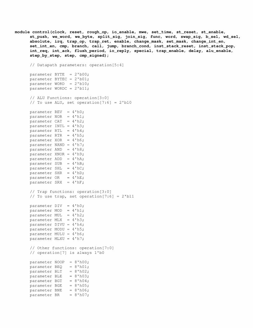
module control(clock, reset, rough_op, io_enable, mwe, set_time, st_reset, st_enable,
st_push, we_word, we_byte, split_sig, join_sig, func, word, swap_sig, b_sel, wd_sel,
absolute, irq, trap_op, trap_ret, enable, change_mask, set_mask, change_int_en,
set_int_en, cmp, branch, call, jump, branch_cond, inst_stack_reset, inst_stack_pop,
int_req, int_ack, flush_period, io_reply, special, trap_enable, delay, alu_enable,
step_by_step, step, cmp_signed);
// Datapath parameters: operation[5:4]
parameter BYTE = 2'b00;
parameter BYTEC = 2'b01;
parameter WORD = 2'b10;
parameter WORDC = 2'b11;
// ALU Functions: operation[3:0]
// To use ALU, set operation[7:6] = 2'b10
parameter REV = 4'h0;
parameter NOR = 4'h1;
parameter CAT = 4'h2;
parameter INTL = 4'h3;
parameter RTL = 4'h4;
parameter RTR = 4'h5;
parameter XOR = 4'h6;
parameter NAND = 4'h7;
parameter AND = 4'h8;
parameter XNOR = 4'h9;
parameter ADD = 4'hA;
parameter SUB = 4'hB;
parameter SHL = 4'hC;
parameter SHR = 4'hD;
parameter OR = 4'hE;
parameter SRX = 4'hF;
// Trap functions: operation[3:0]
// To use trap, set operation[7:6] = 2'b11
parameter DIV = 4'h0;
parameter MOD = 4'h1;
parameter MUL = 4'h2;
parameter MLX = 4'h3;
parameter DIVU = 4'h4;
parameter MODU = 4'h5;
parameter MULU = 4'h6;
parameter MLXU = 4'h7;
// Other functions: operation[7:0]
// operation[7] is always 1'b0
parameter NOOP = 8'h00;
parameter BEQ = 8'h01;
parameter BLT = 8'h02;
parameter BLE = 8'h03;
parameter BGT = 8'h04;
parameter BGE = 8'h05;
parameter BNE = 8'h06;
parameter BR = 8'h07;

parameter JMP = 8'h10;
parameter USER = 8'h11;
parameter RET = 8'h12;
parameter CALL = 8'h13;
parameter RETI = 8'h14;
parameter INT = 8'h15;
parameter JOIN = 8'h16;
parameter SPLIT = 8'h17;
parameter LD = 8'h20;
parameter ST = 8'h21;
parameter LDA = 8'h22;
parameter STA = 8'h23;
parameter POP = 8'h24;
parameter PUSH = 8'h25;
parameter GTIME = 8'h26;
parameter STIME = 8'h27;
parameter IO = 8'h30;
parameter SWAP = 8'h31;
parameter RAND = 8'h32;
parameter WHERE = 8'h33;
parameter GSTP = 8'h34;
parameter SSTP = 8'h35;
parameter STRES = 8'h36;
parameter INRES = 8'h37;
parameter CMPB = 8'h40;
parameter CMPBC = 8'h50;
parameter CMPW = 8'h60;
parameter CMPWC = 8'h70;
parameter CMPUB = 8'h41;
parameter CMPUBC = 8'h51;
parameter CMPUW = 8'h61;
parameter CMPUWC = 8'h71;
parameter SMASK = 8'h44;
parameter UMASK = 8'h45;
parameter DINT = 8'h46;
parameter EINT = 8'h47;
// Control Logic
input clock, reset;
input [7:0] rough_op;
input trap_ret, io_reply, irq, special, step_by_step, step;
output io_enable, mwe, set_time, st_reset, st_enable, st_push, we_word, we_byte,
split_sig, join_sig, word, swap_sig, b_sel, absolute, enable, change_mask, set_mask,
cmp, branch, call, jump, inst_stack_reset, inst_stack_pop, int_req, int_ack,
flush_period, change_int_en, set_int_en, trap_enable, delay, alu_enable, cmp_signed;
output [3:0] func;
output [3:0] wd_sel;
output [2:0] branch_cond;
output [2:0] trap_op;

reg mode = 0; // Supervisor mode register (0 = supervisor, 1 = user)
wire rough_permitted = ~mode;
reg last = 0;
// Generate a pulse on stepping
reg old_step;
always @ (posedge clock) old_step <= reset ? 1'b0 : step;
wire stepper_pulse = step & ~old_step;
reg [7:0] last_op;
reg last_permitted;
reg trap_lock, io_lock, load_lock;
wire delay;
wire no_delay = ~delay;
wire break = (step_by_step ? ~stepper_pulse : 1'b0);
wire [7:0] operation;
assign operation = delay ? last_op : rough_op;
wire permitted = delay ? last_permitted : rough_permitted;
// Signals straight from opcode
wire alu_or_trap = operation[7];
wire trap = operation[6];
assign word = operation[5];
wire const = operation[4];
assign func = operation[3:0];
assign branch = ~| operation[7:4];
assign branch_cond = operation[2:0];
assign trap_op = operation[2:0];
// Signals determined by operation
wire store_abs = (operation == STA) & permitted;
wire load_abs = (operation == LDA) & permitted & ~load_lock;
wire pop_op = (operation == POP);
wire rand_op = (operation == RAND);
wire where_op = (operation == WHERE) & permitted;
wire gtime_op = (operation == GTIME);
wire load = (load_abs | (operation == LD)) & ~load_lock;
assign int_ack = ((operation == RETI) & permitted) & (no_delay & ~break);
assign int_req = (operation == INT) & (no_delay & ~break);
assign absolute = (load_abs | store_abs);
assign b_sel = (const | absolute) & no_delay;
assign io_enable = ((operation == IO) & permitted) & ~(io_reply | break);
assign trap_enable = (alu_or_trap & trap) & ~(trap_ret | break);
assign mwe = (operation == ST) | store_abs;
assign set_time = (operation == STIME) & permitted & no_delay;
assign st_reset = (operation == STRES) & permitted & no_delay;
assign inst_stack_reset = (operation == INRES) & permitted & no_delay;
assign st_push = (operation == PUSH) & no_delay;
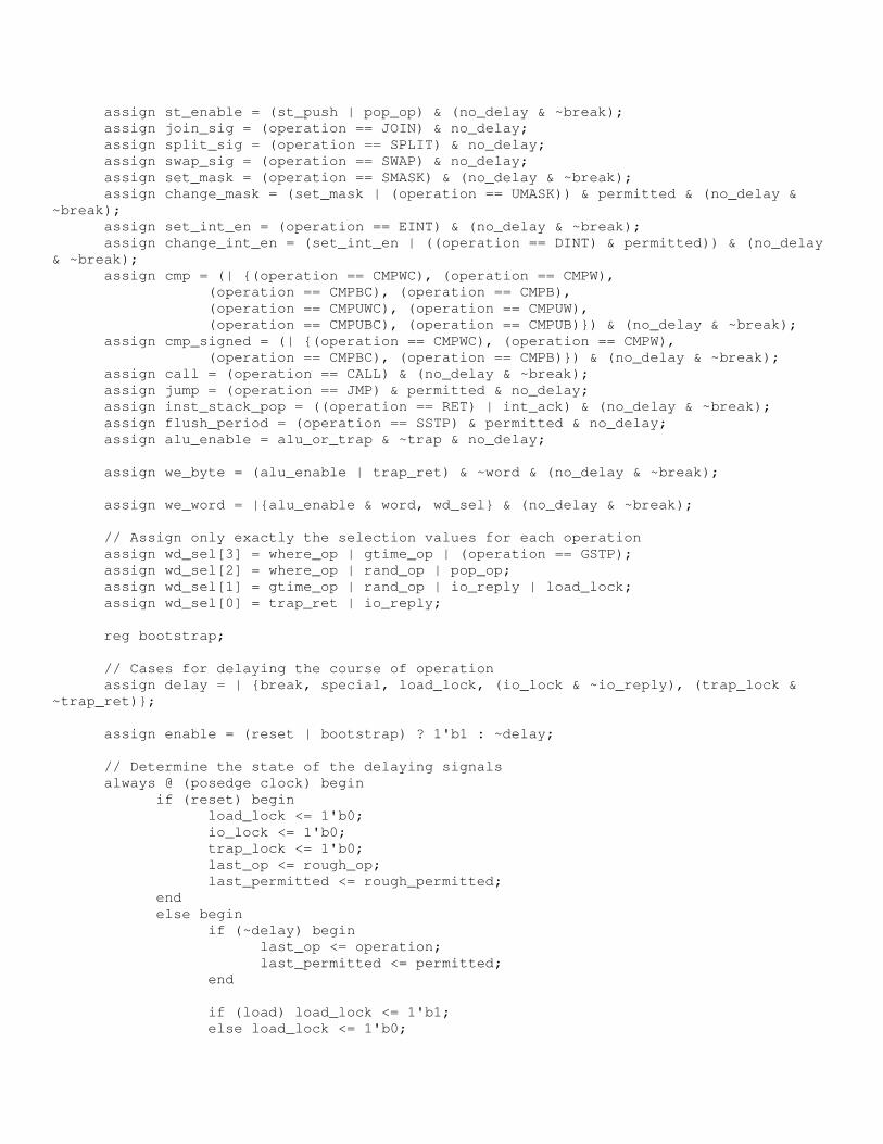
assign st_enable = (st_push | pop_op) & (no_delay & ~break);
assign join_sig = (operation == JOIN) & no_delay;
assign split_sig = (operation == SPLIT) & no_delay;
assign swap_sig = (operation == SWAP) & no_delay;
assign set_mask = (operation == SMASK) & (no_delay & ~break);
assign change_mask = (set_mask | (operation == UMASK)) & permitted & (no_delay &
~break);
assign set_int_en = (operation == EINT) & (no_delay & ~break);
assign change_int_en = (set_int_en | ((operation == DINT) & permitted)) & (no_delay
& ~break);
assign cmp = (| {(operation == CMPWC), (operation == CMPW),
(operation == CMPBC), (operation == CMPB),
(operation == CMPUWC), (operation == CMPUW),
(operation == CMPUBC), (operation == CMPUB)}) & (no_delay & ~break);
assign cmp_signed = (| {(operation == CMPWC), (operation == CMPW),
(operation == CMPBC), (operation == CMPB)}) & (no_delay & ~break);
assign call = (operation == CALL) & (no_delay & ~break);
assign jump = (operation == JMP) & permitted & no_delay;
assign inst_stack_pop = ((operation == RET) | int_ack) & (no_delay & ~break);
assign flush_period = (operation == SSTP) & permitted & no_delay;
assign alu_enable = alu_or_trap & ~trap & no_delay;
assign we_byte = (alu_enable | trap_ret) & ~word & (no_delay & ~break);
assign we_word = |{alu_enable & word, wd_sel} & (no_delay & ~break);
// Assign only exactly the selection values for each operation
assign wd_sel[3] = where_op | gtime_op | (operation == GSTP);
assign wd_sel[2] = where_op | rand_op | pop_op;
assign wd_sel[1] = gtime_op | rand_op | io_reply | load_lock;
assign wd_sel[0] = trap_ret | io_reply;
reg bootstrap;
// Cases for delaying the course of operation
assign delay = | {break, special, load_lock, (io_lock & ~io_reply), (trap_lock &
~trap_ret)};
assign enable = (reset | bootstrap) ? 1'b1 : ~delay;
// Determine the state of the delaying signals
always @ (posedge clock) begin
if (reset) begin
load_lock <= 1'b0;
io_lock <= 1'b0;
trap_lock <= 1'b0;
last_op <= rough_op;
last_permitted <= rough_permitted;
end
else begin
if (~delay) begin
last_op <= operation;
last_permitted <= permitted;
end
if (load) load_lock <= 1'b1;
else load_lock <= 1'b0;
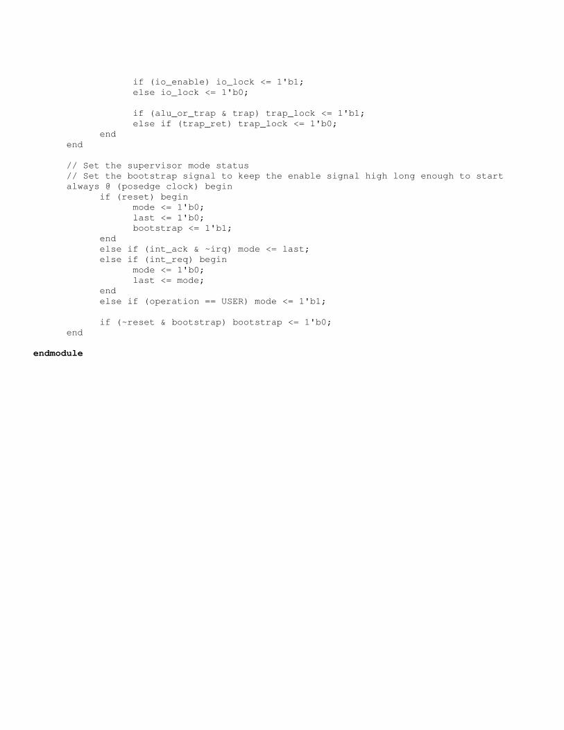
if (io_enable) io_lock <= 1'b1;
else io_lock <= 1'b0;
if (alu_or_trap & trap) trap_lock <= 1'b1;
else if (trap_ret) trap_lock <= 1'b0;
end
end
// Set the supervisor mode status
// Set the bootstrap signal to keep the enable signal high long enough to start
always @ (posedge clock) begin
if (reset) begin
mode <= 1'b0;
last <= 1'b0;
bootstrap <= 1'b1;
end
else if (int_ack & ~irq) mode <= last;
else if (int_req) begin
mode <= 1'b0;
last <= mode;
end
else if (operation == USER) mode <= 1'b1;
if (~reset & bootstrap) bootstrap <= 1'b0;
end
endmodule


