System level simulation of digital designs : a case study
128
University of Cape Town SYSTEM LEVEL SIMULATION OF DIGITAL DESIGNS: A CASE STUDY Grant Carter A dissertation submitted in partial fulfilment of the requirements for the . degree of Master of Science in Engineering (Electrical) University of Cape Town 1998 DIGITISED 2 4 FEB 7016 · ''c'>.;.,;._,.-,_,,,._-. ,, _ '•'' .. The Unlversltv nf C11p1; T:J"•'11 has heen given I the. rig 1 1t. to raproduce t'li-.·; rhe:;ls. in . · or 111 part. C<,pyrigM is held by the .author.
Transcript of System level simulation of digital designs : a case study

Univers
ity of
Cap
e Tow
n
SYSTEM LEVEL SIMULATION OF DIGITAL DESIGNS: A CASE STUDY
Grant Carter
A dissertation submitted in partial fulfilment of the requirements for the .
degree of Master of Science in Engineering (Electrical)
University of Cape Town
1998 DIGITISED
2 4 FEB 7016
~ · ''c'>.;.,;._,.-,_,,,._-. ,, _ '•'' .. ;,;-:.:i~-
The Unlversltv nf C11p1; T:J"•'11 has heen given I the. rig
11t. to raproduce t'li-.·; rhe:;ls. in who~e .
· or 111 part. C<,pyrigM is held by the .author.
~l;>l.-;:"",\~~~~;..;.~.:i_;~~..:N'..·~\i';~~

Univers
ity of
Cap
e Tow
n
The copyright of this thesis vests in the author. No quotation from it or information derived from it is to be published without full acknowledgement of the source. The thesis is to be used for private study or non-commercial research purposes only.
Published by the University of Cape Town (UCT) in terms of the non-exclusive license granted to UCT by the author.

i '
DECLARATION
I declare that this dissertation is my own, unaided work. It is being submitted for the
degree of Master of Science in Engineering in the University of Cape Town. It has
not been submitted before for any degree or examination in any other university.
Signature of Author
Cape Town September 1998
· .. ; -., . - ::·'.'''·i"·•'_"~~"'i':"'~'·-··
ABSTRACT
Very High Speed Integrated Circuit Hardware Description Language (VHDL) is a
hardware description language that is gaining increasing popularity among digital
designers in South Africa, as it is both a synthesis and simulation language. Many
designers make use of the language's synthesis ability but hardly tap into the power
of its simulation abilities. This dissertation primarily investigated the feasibility of
VHDL simulation during the design process. Secondary goals were to document the
design methodology as well as state-of-the-art of the tools required for FPGA
design and simulation. As a case study, a digital preprocessor for a synthetic
aperture radar (SAR) was designed and simulated. The design was targeted for an
FPGA in an attempt to determine the level of complexity of algorithm that can be
obtained in an FPGA. This was a hardware solution to the design requirement; a
completely software solution implemented in a DSP was attempted by Yann
Tremeac [19].
In July 1993, the US Department of Defence instigated a program known as Rapid
Application Specific Signal-processor Prototyping (RASSP). The purpose of this
program was to review the process used in creating embedded digital signal
processors in an attempt to decrease the time taken to produce a prototype by a
factor of four. The methods proposed by RASSP for achieving this goal included
the reuse of existing modules, concurrent design and virtual prototyping.
The virtual prototyping that the RASSP initiative refers to includes a process of
writing VHDL models to represent the system being designed. These models are
first written at an abstract level where the mathematical equations which describe
the processing are tested. Test data can be input to the model which will perform the
required processing. The output can then be verified to ensure that the equations are
correct. At this stage, the model contains no structural information as to how the
processing is achieved, nor even the numerical method used to implement the
equations.
I
-··-,- _____ ,..,. -· :· ·- ~- :· .
The level of abstraction of these models decreases with every model that is written.
Obviously the number and type of models that are written depends upon the design.
An example of the models which could be written are a mathematical model and an
algorithm model which models the numerical methods used in implementing the
mathematical equations. A behavioural or functional model can then be written to
break the system into a number of sub-components. The sub-components are
modelled so that their interfaces are correct but the internals contain no information
on the structure used to implement the algorithms. These models can then be further
refined to include implementation details until a final design is produced. At each
stage, the test data that is used in the more abstract model can still be used for
verification. This system of testing requires that testbenches be written. These are
simply pieces of VHDL code that can read and write data files as well as provide
known stimuli to the unit under test.
To investigate the feasibility of VHDL modelling, a preprocessor for the South
African Synthetic Aperture Radar (SAR) was designed and modelled. This
preprocessor was required to low pass filter the data received by the radar and then
sub-sample it safely to reduce the data rate of the data to be stored. Three methods
were considered for implementing this data reduction: Using a presurnmer, using a
FIR filter or a combination of the two. The last option was chosen since it produced
the highest azimuth resolution after SAR processing and it required the least
number of filter taps to produce. The method required a presurnmer which summed
three PRis. The FIR filter was a 32 tap filter and incorporated a "skip" factor of 4.
This method did not violate any constraints set by the SAR processing regarding the
sampling rate of the data, and it was feasible to implement.
Since the processing was divided into the presurnmer and prefilter, it was logical
that the hardware be similarly divided. One of the first design issues to be overcome
was how these two entities should interact. Both required the use of external RAM
to facilitate temporary data storage. The first method was to have separate
memories for each entity. The presurnmer would then output a presurnmed range
line to the prefilter for processing. The greatest disadvantage of this method was
that the prefilter would then have to store this data in its memory before processing
II
. --~-'·• '"'.
could take place. This was inefficient as the prefilter would have to store the data
again in its memory and this would prevent it from processing during that time. The
second method was the one implemented. The implementation made use of dual
ported RAM. The presummer was connected to one port and the prefilter to the
other. The advantage of this method was that the prefilter did not have to perform
any data storage which increased the amount of time it could spend processing dat~.
An algorithm model was written for the presummer and prefilter operations to
verify the effects of the precision of the stored data, the filter tap weights and the
mathematical validity of the process. Test data was produced and read into the
model. The processed data was output and the results analysed. This data set was
then used to verify the operations of the other more detailed models.
The second model that was written was an abstract functional model. This modelled
the interfaces of the presummer and prefilter but .contained no details of the internal
implementation or timing. The abstract functional model was however able to
process data and the test data which was used in the algorithm simulation was used
to verify the operation of the model. A model of the RAM had to be written to
allow the presummer and prefilter to store data. A functional model was written
which contained no timing information but contained the full functionality of the
device being modelled.
Finally the presummer and prefilter descriptions were written to allow synthesis. A
VHDL synthesiser was used to specify the logic required to implement the devices.
FPGA design software was then used to place-and-route the logic and finally a
FPGA configuration file was produced. Back-annotated VHDL source code was
also produced by the FPGA design software. This was a gate level VHDL model of
the device and included timing information which reflected the internal delays of
the FPGA. This model was used in the test bench for the functional model since it
contained the same I/O ports. The same test data was again used and the results
compared to the functional simulation for verification.
In conclusion, the modelling provided a method of verification that would normally
only be achievable with a physical prototype. The largest problem encountered with
III
...... ,.... . . .,, ":.••"'"'""""'' .-.•:";::" ·.".'"." •.:-,,···.~.~~ .. -~~ ..... ·-··
the virtual prototyping was the simulation time of the gate level models. These
would have taken up to 60 days on an Intel PII-300MHz processor with 196MB
RAM to perform - longer than the time required to build and debug a physical
prototype. The second problem was the availability of VHDL models. Without
simulation models of all the components used, system level simulation was a
pointless exercise. There are some web sites which contain a number of free models
but the majority of available models are commercial and are therefore expensive.
For companies starting out in the field of VHDL modelling, the cost of a VHDL
simulator package can also be prohibitive. If the required models are available and
software to simulate and synthesise them, the goals ofRASSP can be achieved.
N
TABLE OF CONTENTS
ABSTRACT ............................................................................................................................................ !
TABLE OF CONTENTS ..................................................................................................................... V
LIST OF FIGURES ......................................................................................................................... VIII
LIST OF TABLES .............................................................................................................................. IX
ACI<NOWLEDGMENTS .................................................................................................................... X
NOMENCLATURE ........................................................................................................................... XI
CHAPTER l:INTRODUCTION ........................................................................................................ 1
1.1 THESIS OUTLINE ·····•·················································································································· 2
CHAPTER 2: VIRTUAL PROTOTYPING ....................................................................................... 5
2.1 RAPID APPLICATION SPECIFIC SIGNAL-PROCESSOR PROTOTYPING (RAS SP) .......................... 5 2.2 BENEFITS OF VIRTUAL PROTOTYPING ....................................................................................... 6 2.3 VlIDL ........................................................................................................................................ 7
2. 3.1 The History of VHDL ...................................................................................................... 7 2.3.2 VHDL Standards ............................................................................................................. 7 2.3.3 VHDL Software ............................................................................................................... 7
2.4 VlIDL CODING .......................................................................................................................... 9 2.5 VlIDL MODELLING ................................................................................................................. 10
2. 5.1 Temporal Resolution ..................................................................................................... 11 2.5.2 Data Resolution ............................................................................................................. 11 2.5.3 Functional Resolution ................................................................................................... 11 2.5.4 Structural Resolution .................................................................................................... 12 2.5.5 Software Programming Resolution .............................................................................. 12
2.6 GENERAL MODELLING STYLES ............................................................................................... 12 2. 6.1 Behavioural Model.. ...................................................................................................... 12 2. 6.2 Functional Model .......................................................................................................... 12 2. 6.3 Structural Model ........................................................................................................... 12
2. 7 SYSTEM MODELS ..................................................................................................................... 13
2. 7.1 Executable Specification ............................................................................................... 13 2. 7.2 Mathematical Model ..................................................................................................... 13 2. 7.3 Algorithm Model ........................................................................................................... 13
2.8 LOCATION OF MODELS ............................................................................................................ 14
CHAPTER 3: FIELD PROGRAMMABLE GATE ARRAYS (FPGAS) ..................................... 16
3.1 WHATISANFPGA? ................................................................................................................ 16
3.1.l The Logic Cells .............................................................................................................. 17 3.1.2 The 110 Cells ................................................................................................................. 18 3.1.3 The Interconnect Matrix ................................................................................................ 19
3.2 PRODUCINGANFPGADESIGN ............................................................................................... 19
3.2.l Design Entry .................................................................................................................. 19 3.2.2 Logic synthesis .............................................................................................................. 20 3.2.3 Place-and-route ............................................................................................................. 20 3.2.4 ProgrammingtheFPGA ............................................................................................... 21
3.3 DIGITAL SIGNAL PROCESSING IN FPGAs ................................................................................ 21
v
CHAPTER 4: SYNTHETIC APERTURE RADAR ........................................................................ 24
4.1 R.ADARBASICS ......................................................................................................................... 24 4.2 SAR PROCESSING .................................................................................................................... 26
4.2.1 Overview ........................................................................................................................ 26 4.2.2 Image Resolution ........................................................................................................... 27
CHAPTER 5: PREPROCESSOR DESIGN ..................................................................................... 30
5.1 OVERVIEW ............................................................................................................................... 30
5.2 CURRENT SYSTEM ................................................................................................................... 31 5.3 PROPOSED SOLUTIONS ............................................................................................................. 32
5.3.1 Filtering with no Presummer ........................................................................................ 32 5.3.2 Filtering after Presumming ........................................................................................... 32
5.4 FILTERDESIGN ........................................................................................................................ 33 5.5 PREPROCESSORDEVELOPMENT ............................................................................................... 34
5.5.1 Comparing the Proposed Solutions .............................................................................. 35 5.5.2 Finding the Optimal Filter ............................................................................................ 36
5.6 ALGORITHM MODEL ................................................................................................................ 39
CHAPTER 6: HARDWARE DESIGN .............................................................................................. 41
6.1 HARDWARE REQUIREMENTS ................................................................................................... 41
6.2 MEMORY OVERVIEW ............................................................................................................... 42 6.2.1 SeparateMemories ........................................................................................................ 43 6.2.2 Shared Memory ............................................................................................................. 43 6.2.3 Memory Organisation ................................................................................................... 44 6.2.4 Memory Requirements .................................................................................................. 45
6.2.5 Memory Selection .......................................................................................................... 47 6.2.6 VHDLMemoryModel. .................................................................................................. 47
6.3 HARDWARE EXPANDABILITY .................................................................................................. 48 6.3.1 Multiple Output FIFOs ................................................................................................. 49 6.3.2 Writeback to RAM ......................................................................................................... 49
6.4 EXTERNAL INTERFACE ............................................................................................................. 50
CHAPTER 7: PRESUMMER DESIGN ............................................................................................ 51
7.1 FUNCTIONALMODEL ............................................................................................................... 51 7.1.1 Model Functionality ...................................................................................................... 5 2 7.1.2 Presummer Interface ..................................................................................................... 5 2 7.1.3 Model Overview ............................................................................................................ 53 7.1. 4 State Machine ................................................................................................................ 5 6 7.1.5 Verification .................................................................................................................... 57
7.2 FINALIMPLEMENTATION ......................................................................................................... 60
7.2.1 State Machine Encoding ............................................................................................... 60 7.2.2 DC Offset Removal.. ...................................................................................................... 62 7.2.3 Pipelining ...................................................................................................................... 63 7.2.4 Component Instantiation ............................................................................................... 65 7.2.5 Verification .................................................................................................................... 66 7.2.6 Target Device ................................................................................................................ 68
CHAPTER 8: PREFILTER DESIGN ............................................................................................... 69
8.1 THE FUNCTIONAL MODEL ....................................................................................................... 69 8.1.1 ModelFunctionality ...................................................................................................... 69 8.1.2 Prefilter Interface .......................................................................................................... 70 8.1.3 Model Overview ............................................................................................................ 70 8.1.4 State Machine ................................................................................................................ 72 8.1.5 Verification .................................................................................................................... 73
8.2 FINAL IMPLEMENTATION ......................................................................................................... 75 8.2.l State Machine ................................................................................................................ 75 8.2.2 FIR Filter ....................................................................................................................... 76
VI
8.2.3 Dividers ......................................................................................................................... 77 8.2.4 DC Offset ....................................................................................................................... 79 8.2.5 Verification .................................................................................................................... 80 8.2. 6 Target Device ................................................................................................................ 81
CHAPTER 9: CONCLUSIONS AND RECOMMENDATIONS .................................................. 82
APPENDIX A: FIR FILTER CHARACTERISTICS .................................................................. 84
A.1 FILTERA .................................................................................................................................. 85 A.2 FILTERB .................................................................................................................................. 86 A.3 FILTERC .................................................................................................................................. 87 A.4 FILTERD .................................................................................................................................. 88 A.5 FILTERE .................................................................................................................................. 89 A.6 FILTERF ................................................................................................................................... 90 A. 7 TABLE OF FILTER COEFFICIENTS .................................. ········ ................................................... 91
APPENDIX B: JTAG BOUNDARY SCAN .................................................................................. 93
APPENDIX C: MAIBCAD SAR PROCESSOR ......................................................................... 94
APPENDIX D: VHDL CODE DESCRIPTION .......................................................................... 100
D.l TESTDATAGENERATOR ....................................................................................................... 100 D.2 RAMMODEL. ........................................................................................................................ 100 D.3 PRESUMMERCODE ................................................................................................................ 101
D.3.1 Algorithm Model ......................................................................................................... 101 D.3.2 Functional Model ........................................................................................................ 102 D.3.3 SynthesisModel.. ......................................................................................................... 102 D.3.4 Presummer Testbench ................................................................................................. 104
D.4 PREFILTERCODE .................................................................................................................... 104 D.4. 1 Algorithm Model ......................................................................................................... 104 D.4.2 Functional Model ........................................................................................................ 105 D.4.3 Synthesis Model.. ......................................................................................................... 106 D. 4. 4 Prefilter Testbench ...................................................................................................... 10 7
REFERENCES ................................................................................................................................... 109
BIBLIOGRAPHY .............................................................................................................................. 112
VII
LIST OF FIGURES
Number
Figure 1: VHDL Entity Architecture Pairs Figure 2: FPGA Internals Figure 3: Radar Timing Relationships Figure 4: Illuminated Ground Area of a Side Looking Airborne Radar Figure 5: Block Diagram of SAR Processing Figure 6: FIR Filter Skip Factor Figure 7: Filter Response Comparison Figure 8: Processed SAR Data for Filter C Figure 9: Algorithm Model Block Diagram Figure 10: Block Diagram of Separate Memory Solution Figure 11: Block Diagram of Shared Memory Solution Figure 12: Memory Organisation-Data Stored in Range Figure 13: Memory Organisation- Data Stored in Azimuth Figure 14: Top Level Block Diagram of the Prefilter Figure 15: Presummer Model Overview Figure 16: RAM Address Counter Figure 17: Effects on RAM Accesses from RAM Counter Increments Figure 18: Block Diagram of Presummer Figure 19: Presummer State Machine for Functional Model Figure 20: Presummer Testbench Figure 21: Presummer State Machine for Final Implementation Figure 22: Non Pipelined Four Input Adder Figure 23: Pipelined Four Input Adder Figure 24: Presummer Data Path Figure 25: Prefilter Model Overview Figure 26: Block Diagram of Prefilter Figure 27: Prefilter State Machine Figure 28: Prefilter Testbench Figure 29: Frequency Response of Filter A Figure 30: Coefficients ofFilter A Figure 31: Frequency Response of Filter B Figure 32: Coefficients of Filter B Figure 33: Frequency Response of Filter C Figure 34: Coefficients ofFilter C Figure 35: Frequency Response of Filter D Figure 36: Coefficients of Filter D Figure 37: Frequency Response of Filter E Figure 38: Coefficients of Filter E Figure 39: Frequency Response of Filter F Figure 40: Coefficients ofFilter F
VIII
Page
10 18 25 25 27 34 38 38 40 43 44 45 46 50 51 54 55 56 58 59 61 63 64 64 69 71 74 75 85 85 86 86 87 87 88 88 89 89 90 90
. ····: .... ,._,,. , • .,, •. _.,,-_-_-"--,-'_::c'"_;_' ___________ __;___;_--'--------'---'-"-'-" :;__•···~·"___;_ ___ _;_ _____ ,_, --"-"""'"-" ....... ,_ .. ,_, -------· ---... , ,,..-,,._-,,_,, ·-·--... ·~~ ... --.... ·-· -

LIST OF TABLES
Number
Table 1: Radar Specifications Table 2: Initial Test Filter Perfonnance Table 3: Final Filter Perfonnance Table 4: Presummer Interface Pins Table 5: Prefilter Interface Pins Table 6: FIR Filter Coefficients
IX
Page
30 36 37 52 70 91

ACKNOWLEDGMENTS
The author wishes to thank the following people: ·
• Prof. Mike Inggs for his guidance and constructive comments.
• Stefan Rousseau for his help on VHDL coding issues.
• Peter Fenn for his assistance with VHDL.
• Jasper Horrell for his assistance with the SAR processing, his comments and
advice.
• Alan Langman for his ideas and guidance.
• Gavin Doyle for the use of his computer, donated by the Department of Water
Affairs.
• Richard Lord for his advice and assistance.
• Yann Tremeac for his help with the filters, DSP solutions and advice.
• Dr. Pieter Bakkes for allowing me access to the Synopsys Design Software.
• Graham Jack for his comments and advice.
Their help has been invaluable and is greatly appreciated.
x
ABEL
AHDL
ALU
ASIC
DSP
EDA
FFT
FIR
FPGA
HDL
LPM
LSB
LUT
MSB
PCB
RAS SP
RTWG
1 ......... . ..,-.. ·.'}·~···· '·· ... ,
NOMENCLATURE
Advanced Binary Expression Language. An HDL written by Data
IIO
Altera Hardware Description Language. An HDL written by
Altera
Arithmetic and Logic Unit
Application Specific Integrated Circuit. A custom digital IC
Digital Signal Processor
Electronic Design Automation
Fast Fourier Transform
Finite Impulse Response. A type of digital filter
Field Programmable Gate Array
Hardware Description Language
Library of Parameterised Modules
Least Significant Bit
Lookup Table
Most Significant Bit
Printed Circuit Board
Rapid Application Specific Signal Processing
RASSP Taxonomy Working Group
XI
SAR
Taxonomy
Verilog
VHDL
VLSI
Synthetic Aperture Radar
Classification
A HDL which is similar to VHDL
Very High Speed Integrated Circuit Hardware Description
Language
Very Large Scale Integration
XII
Chapter 1 : Introduction
Chapter 1: Introduction
VHDL is a hardware description language that is gaining increasing popularity with
digital designers, as it is both a synthesis1 and simulation language. The majority of
users in South Africa today use only the language's synthesis abilities, hardly ever
tapping into the power of simulation. Their systems design is modular and although
their modules are tested, it is not known before the design is prototyped how the
modules will function in the completed system. In South Africa, VHDL is used
mostly for FPGA design. Most of the more popular FPGA design software
packages have very limited VHDL simulation abilities. The system therefore cannot
be tested before it is completely implemented.
With the fierce competition between companies to get their products onto the
market, the design's time-to-market must be minimised. Finding design errors
during physical prototyping leads to costly delays, both financial and timely. It
would be far cheaper if the designs could be debugged and tested before reaching
silicon for the first time. The solution is Virtual or System Level Prototyping.
Virtual Prototyping involves the simulation of the entire system. The level of
complexity can be from a behavioural (top level), right down to a gate level
simulation. The lack of use of Virtual Prototyping in smaller companies often is due
to them not having sufficient resources to develop their own models of the
components they wish to simulate. This is becoming less of a problem due to the
rapidly increasing popularity of the World Wide Web. VHDL models can now be
obtained for a variety of digital devices, from TTL and CMOS gates to models of
processors that will execute given instruction code. Many specialist companies are
publishing on the Web with their sole area of business being the development of
such models. Companies are now able to purchase the models they require, rather
than spending hundreds of man-hours developing them.
1 Synthesis is the process of specifying digital logic gates that will be functionally equivalent to a specification of hardware described in a hardware description language.
1
Chapter 1 : Introduction
This thesis will attempt to investigate the feasibility of VHDL simulation. As a case
study, the design of a digital preprocessor for a synthetic aperture radar was
attempted. The preprocessor was designed and simulated in VHDL.
The preprocessor was targeted for a Field Programmable Gate Array (FPGA). The
reason for this was to investigate the level of complexity of algorithm that could be
achieved in such a device. This solution was completely hardware based. A
software based digital signal processor (DSP) solution is being investigated by
Yann Tremeac [19].
1.1 Thesis Outline
This thesis is divided into 9 chapters and 4 appendices. A brief overview of each
chapter and appendix follows:
Chapter 2 introduces Virtual Prototyping, which is part of a new design process
called RASSP. Rapid APplication §pecific §ignal-processor frototyping is a design
methodology which aims to reduce the typical development time of a DSP system
from months to a period of weeks. Virtual prototyping is also becoming a necessity
owing to the increased pin counts of some of the new high density IC packages. It is
no longer feasible for a "bed-of-nails" tester to test boards containing such devices
and plugging a logic analyser into the system is almost impossible as the new
packages often contain no pins e.g. Ball Grid Arrays. Virtual prototyping is required
to test the internals of each of the PLDs while boundary scan techniques will test
their interconnection. The chapter also introduces VHDL, a Hardware Description
Language which can be used for both the simulation and synthesis of digital
circuits. System components can be modelled with VHDL and chapter 2 describes
the different levels of abstraction of these models. How each is used in the virtual
prototyping process is also described.
Chapter 3 describes Field Programmable Gate Arrays and the design process
required to produce the configuration files for programming them. Most FPGA
manufacturers have design software for their specific devices. These packages will
often compile a VHDL description of the device and then synthesise the logic
2
Chapter 1 : Introduction
required to implement it. This logic is then place-and-routed and a configuration file
for the FPGA is produced. Many of the new FPGAs are SRAM based and required
a specialised serial ROM to load their configuration on power up. The use of
FPGAs in a DSP environment is also discussed.
Chapter 4 introduces some basic synthetic aperture radar theory. Since the focus of
this thesis is not SAR processing, the theory contained in this chapter will not be
very detailed. An overview of the workings of a pulsed radar will be described.
Once the transmitted data has been received, it requires processing to convert it into
a focussed image. In order to do this, the data has to be compressed in azimuth, so
that the individual targets can be seen. Chapter 4 describes this process.
Chapter 5 details the filter development. This chapter begins by looking at why the
preprocessor was needed and how its specifications were decided upon. At this
stage of development, no consideration was given to the hardware. The
preprocessor was required in an existing radar to reduce the data rate of the data
being stored. By low pass filtering the data, it could safely be subsampled. Three
main methods were examined: Using only a presummer, using a presummer before
a FIR filter and using just a FIR filter. All of these methods were tested and the
results are included. Using a presummer before the FIR filter was the method
decided upon as it allowed for the use of a filter with a better cutof£ This produced
a better focussed image.
Chapter 6 discusses the preprocessor' s hardware development. A top down
approach was used during development to keep in line with the principles of
RASSP. Without specifying the internals of either the presummer or prefilter, some
decisions had to be made regarding the hardware requirements, especially for the
memory. The expandability of the solution had to be determined as the processing
speed of the presummer and prefilter would not be known until it was designed. A
solution which could be made to meet the speed requirements had to be found.
Chapters 7 and 8 describe the design of the presummer and prefilter FPGAs. A top
level, behavioural simulation was first performed to verify the correctness of the
algorithms. Once this was verified, separate high level models of the presummer
3

Chapter 1 : Introduction
and prefilter were constructed. This allowed the interaction of the components to be
tested and the system could then be compared with the original algorithm. The
presummer and prefilter were then implemented separately as synthesisable VHDL
models. Once implemented, the components were then tested against the results
produced by the original algorithmic simulation. The final design could therefore be
verified without the need for physical prototyping.
Chapter 9 contains the conclusions. Virtual Prototyping has distinct advantages
when building systems, whether it be simple micro-controller boards to complete
digital radars. The ability to simulate each of the devices and to be able to probe any
point in the system saves a great deal of time when debugging systems. Finding
errors is far quicker when looking at the results of a simulation than having to use
conventional hardware techniques such as logic analysers. Correcting errors is also
far cheaper when discovered before the printed circuit boards are made. Depending
on the simulator used, the number of existing VHDL models available to the
designer varies. Producing models is a time consuming task and it would be
pointless for small companies to employ a designer to code only the models
required.
Appendix A contains the specifications for the different filters considered. The
specifications include the tap weights, sampling frequency and cut-off frequency.
Appendix B contains brief description of the JTAG standard for programming
FPGAs and for use in Boundary Scan.
Appendix C contains the MathCAD simulation used for comparing the effects of
the filters on the SAR processing.
Appendix D contains the VHDL source code for the simulations and synthesised
FPGA.
4
Chapter 2: Virtual Prototyping
Chapter 2: Virtual Prototyping
Virtual prototyping is known by a variety of names including board level
simulation, system simulation and rapid prototyping. Virtual prototyping can be
defined as "simulating the functionality of one or several printed circuit boards built
with standard components, possibly incorporating Application Specific Integrated
Circuits, ASIC, and Application Specific Standard Products, ASSP" [8]
2.1 Rapid Application Specific Signal-processor
Prototyping (RASSP)
Virtual prototyping is the basis for Rapid Application Specific Signal-processor
Prototyping (RASSP). This program was initiated by the Defence Advanced
Research Projects Agency (DARPA) in July 1993 with the aims of significantly
improving the process by which embedded digital signal processors are developed
and supported [17]. The program also emphasises design reuse in an effort to
further reduce the development time of subsequent projects or upgrades. RASSP
aims at reducing the time taken to field a prototype by a factor of four with respect
to conventional design methodologies. One of the main reasons behind this program
was that systems were designed using state-of-the-art devices, but by the time the
system went into production, the devices were obsolete [15].
The RASSP methodology is based on two principal ideas: Concurrent design and
design reuse [13]. The former specifies the idea that software and hardware should
be developed in parallel and not serially, as is often the case. The hardware should
also be developed in parallel with separate teams designing different modules of the
design. Design reuse is also critical to this program as it is pointless repeating work
which has already been done.
5
Chapter 2: Virtual Prototyping
To test the claims of the RASSP program, a series of benchmarks were established.
The first two required the development of a virtual prototype and a hardware
prototype respectively for a Synthetic Aperture Radar Processor.
2.2 Benefits of Virtual Prototyping
Virtual prototyping encourages a top-down design methodology. This allows the
entire system to be modelled at first on a very abstract level where the basic
workings of the system can be verified. Once it is determined that the system will
meet the processing requirements i.e. the algorithm to be implemented is correct,
more specific and detailed models can be developed to replace the abstract ones.
During this process, the system can be divided into modules and the specifications
of each can be defined. By doing this at an early stage, the functionality of the
modules can be tested, as well as their ability to interact with the other modules. By
moving to lower levels of model abstraction, different architectures can be
evaluated before one is finally chosen.
Virtual prototyping also allows for the simulation of subsystems which have not
been fully implemented. This allows designers to test their individual modules with
the modelled system, even if the entire system has not been implemented. Doing
this enables the verification of each model within the system environment. As more
modules are implemented, so their models are updated with more accurate ones
(lower abstraction level).
Hardware and software partitioning has also been improved with the use of virtual
prototyping. Under "traditional" development, once the hardware had been
prototyped, the software could be developed.
Virtual prototyping allows a more thorough verification of the hardware than would
be achieved using conventional hardware testing methods. One of the reasons for
this is that virtual prototypes can be probed in many more places than conventional
test hardware. Using these models will also allow the test engineer to test for
conditions that are difficult to produce in the real hardware.
6
Chapter 2: Virtual Prototyping
2.3 VHDL
Very High Speed Integrated Circuit Hardware Description Language is a hardware
description language (HDL) which is rapidly gaining popularity as both a
simulation and synthesis language.
2.3.1 The History of VHDL
In 1980 the US Department of Defence (DoD) funded a project under the Very
High Speed Integrated Circuit (VHSIC) project to create a standard Hardware
Description Language (HDL). The reason for this was the DoD's desire to obtain a
standard design and documentation tool. The result of this was the creation of the
VHSIC HDL, or VHDL as it is now commonly referred to [11].
2.3.2 VHDL Standards
VHDL is an IEEE standard and had undergone one rev1s1on. VHDL was
standardised in 1987 by the IEEE and was referred to as VHDL 1076-87. It was
revised in 1993 (VHDL '93) and most VHDL software packages use this version
today. There are not many significant differences between the two versions except
for file 110. Under VHDL '87 there was no way to explicitly open and close a file.
This has been remedied in VHDL '93.
Synopsys, a company who are the industry leaders in ASIC design software
including VHDL compilers and synthesisers, have written some VHDL libraries
which have now become fairly standard and are packaged with most VHDL
simulators. These additions deal mostly with the file 110 of formatted text.
2.3.3 VHDLSoftware
Once compiled, VHDL source files can be synthesised or simulated. These two
processes are very different and often not both fully supported in some software
packages.
VHDL synthesis involves taking a VHDL source file and synthesising the digital
logic that the source file describes. Not all synthesisers are created equal and one of
the characteristics which separates the good from the bad synthesisers is their ability
7
Chapter 2: Virtual Prototyping
to optimise the logic they have created. Thus, the logic that they produce will be
less efficient than from a good compiler in speed and/or area. Many FPGA
manufacturers provide VHDL synthesisers with their FPGA design software but
licences for these often have to be purchased separately.
A full simulator should be either VHDL '87 or VHDL '93 compliant. VHDL
simulators are sometimes packaged with synthesisers but often in a stripped down
version. These simulators are normally graphical simulators where the inputs have
to be entered graphically- not written as a VHDL input file. This is very limiting in
that writing a VHDL description for a given waveform is far easier than entering it
graphically, especially when it is repetitive. These simulators usually do not have
any support for file 1/0 and so test benches cannot be written to verify any data
produced.
A number of different vendors produce VHDL Simulators. Some of these have
demonstration versions of their software which may be evaluated for a short period.
All except Ptolomy and Alliance are commercial packages.
• ActiveVHDL (http://www.aldec.com/ActiveVHDL)
• Alliance. This is a freeware VHDL teaching aid which supports some of the
VHDL subset. (http://www-asim.lip6.fr/alliance/index.gb.html)
• Mentor Graphics (http://www.mentorg.com)
• Model Technology's ModelSim (http://www.model.com)
• PeakVHDL (http://www.acc-eda.com)
• Ptolemy. This is written by the Ptolemy Project at the University of California
at Berkeley. (http://ptolemy.eecs.berkeley.edu/)
• Synopsys (http://www.synopsys.com)
8

Chapter 2: Virtual Prototyping
2.4 VHDL Coding
Describing the VHDL language is far too great a task to perform here. What follows
is a brief introduction into the structure of the language. The main programming
unit in VHDL source is the entity-architecture pair (see Figure 1). An entity is the
description of the interface ports of a design e.g. the pins on an IC. This entity has
an architecture associated with it that describes the working of the entity. If an
entity is required as part of another entity, it is referred to as a component and is
declared as such.
An entity can have multiple architectures associated with it, although only one
architecture may be used at any one time. A configuration is required to bind an
architecture with an entity (see Figure 1). lfthere is no explicit configuration, the
default configuration is used.
VHDL source written for simulation cannot always be synthesised. In fact, only a
small subset of the language is synthesisable. This alone is reason enough for
having multiple architectures. For the same entity, synthesisable and simulatable
architectures can be written. Depending on which process is being performed, either
of the two architectures can be selected in the configuration (see Figure 1).
9

Chapter 2: Virtual Prototyping
Entity
~Configuration Simulation
Architecture
Synthesis
Architecture
Component
Figure 1: VHDL Entity Architecture Pairs
Entity
Architecture
The style of writing VHDL will also affect the logic that is synthesised. Although
two ways of writing some code will have the same logical effect, the logic
synthesised could be completely different. For example, using a "case" statement is
more efficient than using nested "if' statements. The former is often synthesised as
a multiplexer while the latter results in a string of nested AND gates.
Writing synthesisable VHDL cannot be compared with writing a program m
another software programming language like "C" or even simulation VHDL. One
must always remember that one is writing hardware and that the source which is
written is going to be transformed into hardware. Writing code without considering
the hardware that will be generated will result in code with either does not
synthesise or does not perform as expected. An example of this causes latches to be
inferred if signals are not assigned default values.
2.5 VHDL Modelling
A VHDL model of a device is a description written in VHDL which describes the
operation of the device at a particular level of abstraction. To introduce
standardisation into the writing of VHDL models, the RASSP Taxonomy Working
Group (RTWG) was formed in 1995. Their mission was to "develop a systematic
10
Chapter 2: Virtual Prototyping
basis for defining VHDL model types and to use this basis for concisely and
unambiguously defining a terminology that describes the models that are used
within a RASSP design process" [14].
To describe a VHDL model, the RASSP Taxonomy differentiates between five
orthogonal model characteristics: Temporal detail, data value detail, functional
detail, structural detail and software programming level. Each of these
characteristics is applied to the internal and external views of the model. These can
be plotted on a set of axes [14] that describes the level of abstraction of each of
these model characteristics. A brief explanation of these characteristics can be
found below.
2.5.1 Temporal Resolution
The Temporal Resolution Axis represents the time scale of the events that are
modelled [14]. For example if one is wishing to capture the timing of the gate
delays, the temporal resolution of the model could be in the order of picoseconds.
If, on the other hand, the instruction cycles were to be modelled, the temporal
resolution of the model could be in the order of milliseconds.
2.5.2 Data Resolution
The Data Resolution Axis represents the resolution of the format of the data values
that are used [14]. For example, if the value 1 was to be represented, it could be
done so on a low level as a binary string "0001". The same number could be
represented as an integer (1) or as an enumerated type e.g. Yellow. All these
representations are equally accurate, just increasingly abstract.
2.5.3 Functional Resolution
The Functional Resolution Axis represents the level of detail at which the model
describes the functionality of the component or system [14]. This can range from
Boolean expressions that specify the logic required to implement a function to the
mathematical representation of that function.
11
Chapter 2: Virtual Prototyping
2. 5. 4 Structural Resolution
The Structural Resolution Axis represents the level of detail that a model provides
about how it is constructed out of constituent parts [14]. For example, if the
structure of an IC were being modelled, a high resolution model would describe the
IC in terms of the logic gates which make it up. A low resolution model would
describe an IC in terms of ALUs, multiplexers and registers.
2. 5. 5 Software Programming Resolution
The Software Programming Resolution Axis represents the granularity of the
instructions a model can execute when running the target software [14]. The
resolution can range from microcode instructions to high level operations like an
FFT.
2.6 General Modelling Styles
For a complete discussion of VHDL modelling, the reader is urged to consult [14]
as it provides a complete reference for all types ofVHDL models, not only the ones
introduced here. All VHDL models are described in terms of three primary classes.
Each of these uses the axes described in Section 2.5 to describe their resolution.
2. 6.1 Behavioural Model
This model describes the functionality and timing of a component without
specifying a particular implementation. It can be thought of as a functional model
with timing. A behavioural model can exist at any level of abstraction - this being
determined by the resolution of the implementation details [14].
2.6.2 Functional Model
This model describes the function of the system without introducing timing. It is
essentially a behavioural model without the timing. Like the behavioural model, the
functional model can exist at any level of abstraction [ 14].
2.6.3 Structural Model
A structural model describes a component or system in terms of the interconnection
of sub-components. The model shows the structure of the physical implementation.
12
.. .. . . . .,,, . ' . -·. . ... , ... ,,..,...,., ....... , """:" . ' -.~,, .... - '" . '" . . . " . ··; .. ,., "
Chapter 2: Virtual Prototyping
For example, a structural model of a processor would show, among other things, an
ALU connected with some registers and a program counter. These sub-components
can be described behaviourally, functionally or structurally [14].
2. 7 System Models
The RTWG defines three terms for use in describing models that represent digital
systems. These models contain no structural information regarding the
implementation of the system.
2. 7.1 Executable Specification
This model is a behavioural description of the system or component and mirrors the
particular functionality and timing of the required system or component. Other
system metrics e.g. weight, power consumption and size can be included in this
model [14].
2. 7.2 Mathematical Model
The mathematical model describes the functional relationship between the input and
output data values. This relationship described in purely mathematical terms but
does not contain any indication as to which mathematical method is used in the
computation. This description can be found in the algorithm model [14].
A mathematical model is written to test the mathematics behind the processing to
verify that they are correct. Once this is verified, an algorithm model can be written
to test various implementations of the mathematics.
2. 7.3 Algorithm Model
This is similar to the mathematical model in that it too describes the relationship
between the input and output data values. The difference is that the algorithm model
also describes how the results are calculated i.e. using Newton's method or a
Mc Lauren Series [ 14].
13
Chapter 2: Virtual Prototyping
An algorithm model is used to test the efficiency and validity of a number of chosen
mathematical methods. This model is also used to test the required precision of data
values.
2.8 Location of Models
There are a number of sources of VHDL models. Most of these are on the World
Wide Web and the designer is able to download the model(s) he/she is looking for.
Certain VHDL Simulator Manufacturers provide models for use with their software.
Synopsys (http://www.svnopsvs.com) is one such company and probably have the
largest selection of models. The following lists a number of web sites which contain
either freeware or shareware models.
• The RASSP Home Page (http://rassp.scra.org) has a number of VHDL models.
These include processor, memory and bus models and are available for free
download.
• The Free Model Foundation provides some free and other commercial
models. (http://vhdl.org/fmfil
• The Hamburg VHDL Archive provides freeware and shareware models.
(http://tech-www.infom1atik.uni-hamburg.de/vhdl/vhdl.html)
• The University of Strasbourg has a free model archive. (http://erml .u
strasbg.fr/db)
• The Microsystems Prototyping Laboratory at Mississippi State University
has some free VHD L models.
(http://www.erc.msstate.edu/mpl/vhdl/html/models/index.html)
• Doulos VHDL Model Library have some free behavioural models.
(http://www.doulos.co.uk/models/index.htm)
14
Chapter 2: Virtual Prototyping
A number of commercial model developers also have web sites. Since these models
have to be paid for before they can be evaluated, the quality of these sites has yet to
be determined.
15
-. ' - .. ,) .,. . ., ' . - ... : .. ';, :····.,··-"•rt·.·••., ; ~ :~'.""'.'; . ,
Chapter 3: Field Programmable Gate Arrays (FPGAs)
Chapter 3: Field Programmable Gate
Arrays (FPGAs)
Field Programmable Gate Arrays (FPGAs) are programmable logic devices which
provide the benefits of custom CMOS VLSI, while avoiding the initial cost, long
development cycle and inherent risk of a conventional masked gate array [20].
3.1 What is an FPGA?
When custom digital logic is required in a design, the designer is provided with a
number of options ranging from ASICs to discrete logic. ASICs are expensive to
design but their unit price is low since the size of the minimum order is usually very
big. The designer specifies the logic required in the IC and the manufacturer
produces it from a design file. An FPGA is a type of ASIC except that the designer
can configure the logic within the device to implement the required functionality.
The FPGA effectively provides the designer with a "sea of logic gates" which is
configured by the designer. This process has the effect of connecting the logic gates
in such a way that the required logic functions are produced. The unit price of an
FPGA is more than an ASIC but FPGAs are available in smaller quantities. The
initial cost of production is less for an FPGA than an ASIC since the internals of the
former are already specified. All that is required is for the device to be configured to
produce the required functionality. When designing an ASIC, the entire design of
the device is left to the designer. More skill is therefore required to design an ASIC
than to produce an FPGA. FPGAs are often used as prototypes for ASICs. The
FPGAs can be programmed to provide the same functionality as the ASICs for
testing purposes.
16
., ·,.-., ...,.,,.., ............ - ··-:·''·'

------------------------------------------------
Chapter 3: Field Programmable Gate Arrays (FPGAs)
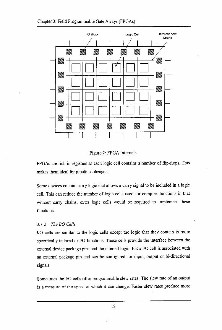
Different manufacturers have different structures for their devices but essentially
they share the same basic idea2. There are three parts: the logic cells, the I/O cells
and the interconnection matrix. These are illustrated in Figure 2.
Many FPGAs are SRAM based and read their configuration from an onboard ROM
on power up. This has a number of advantages:
• Bug fixes can be perfonned by simply reprogramming the configuration ROM.
• The FPGA can be forced to reconfigure "in system" to allow it to perfonn
different tasks as required [10] e.g. if the FPGA contained a FIR filter, new
coefficients could be loaded if required. These configurations would have to be
stored onboard and could not be created "on the fly''.
• For applications where the security of the internal design is critical, the contents
. of both the ROM and the FPGA can be erased should the unit be tampered
with. Once erased, no reverse engineering can take place as no clue as to the
operations of the device will remain.
3.1.1 The Logic Cells
The logic cells are blocks of logic that can be configured to produce the user's
required logic functionality. These logic cells contain flip-flops and some logic
function generators which are usually implemented as lookup tables.
The LUTs have a set number of inputs but still provide incredible flexibility since
logic cells can be combined with the interconnect matrix. This allows multiple
LUTs to be used to generate a single function.
In some FPGAs, RAM and ROM are available to the designer. These memory
devices are sometimes implemented in the LUTs in the logic cells (e.g. Xilinx),
while other devices have separate cells to implement them (e.g. Altera).
2 The description below is essentially what the two market leaders in FPGA technology, Xilinx Inc. and Altera Corp. use.
17
• ·--: •• )" , .... - ..... J •• ,.,. ..... ~···•: •••••• ,. •• .:"""'.'•--···• ,, ..• ,,,.-~ .•• , . .,,..;·~-.,.,·~···:·-:.·~•:.•·"·~·~·o•,1,,,., ······:-.··~.,,n·•••-·'' '•°''· • · ,··--;•,,,.,.,.,.. •••.. ~,~ •. , .• , .. :;r .. -;;·, ., .. ., ..•. .,:·-::••7•->...,...::.-: .. ~·
Chapter 3: Field Programmable Gate Arrays (FPGAs)
110 Block Logic Cell Interconnect Matrix
• • • • ~ • • • • D D D L] D D • D D D D D D • • D D D D D D • • • D D D D D D • • • • • • • • • Figure 2: FPGA Internals
FPGAs are rich in registers as each logic cell contains a number of flip-flops. This
makes them ideal for pipelined designs.
Some devices contain carry logic that allows a carry signal to be included in a logic
cell. This can reduce the number of logic cells used for complex functions in that
without carry chains, extra logic cells would be required to implement these
functions.
3.1.2 The IIO Cells
I/O cells are similar to the logic cells except the logic that they contain is more
specifically tailored to I/O functions. These cells provide the interface between the
external device package pins and the internal logic. Each I/O cell is associated with
an external package pin and can be configured for input, output or bi-directional
signals.
Sometimes the I/O cells offer programmable slew rates. The slew rate of an output
is a measure of the speed at which it can change. Faster slew rates ·produce more
18
.... ,__, ·-· ... ,. ..•• .. .. ,, . ,, . ·, .·----~-··--;::·:·:~·· .. · ..... 1·;~:-·· ~ ..... _, .
l ...... ~····· .. '
Chapter 3: Field Programmable Gate Arrays (FPGAs)
noise than slower slew rates. Depending on the application, the designer can choose
which slew rate to use.
Many applications require that the inputs and outputs be registered. In an effort to
minimise the setup time on inputs and the clock to output time on outputs, the 110
cells often have flip-flops in them. The advantage of using these flip-flops as
opposed to any others in the FPGA is that the distance between the pin and the flip
flop is minimised. This reduces the routing delay and hence the setup and hold
times of the pin.
3.1.3 The Interconnect Matrix
The logic cells and I/O cells are connected together with a routing matrix. This
matrix provides a means of connecting cells to each other. Different vendors have
different methods of providing routing and most claim that their devices are more
"routable" than their competitors, especially when referring to pin locking. Pin
locking is when the designer forces the FPGA design software to place certain input
and output signals on specified pins. When the FPGA is initially designed, these
signals are placed on the pins that are most optimal in terms of routing. Should the
design be changed after the PCB had been designed, it is essential that the FPGA
use the original pins for its signals. Obviously, this problem increases as the
utilisation of the FPGA increases.
3.2 Producing an FPGA Design
FPGA vendors produce software that is used in design of their own devices. The
device specific stage of the design is the fitting or place-and-routing. Third party
software is available to perform the design entry and logic synthesis but the author
has not encountered any which can perform any device fitting.
3.2.1 Design Entry
This is the first stage in the design. Two methods exist for doing this: graphical or
HDL entry. Graphical entry is cumbersome with larger designs and is less flexible
than HDL entry. Symbols for various logic functions (logic gates, multiplexers,
adders etc.) are connected together by the designer. This method is useful if a
19
Chapter 3: Field Programmable Gate Arrays (FPGAs)
schematic for the required logic already exists but becomes very cluttered with
larger designs.
HDL entry is not limited to using VHDL. ABEL, AHDL and Verilog are examples
of other hardware description languages that can be used for describing the
operation of the device. Different design software supports different HD Ls but most
seem to offer VHDL support-usually as an optional extra.
Once the design has been entered, it has to be compiled. This checks the syntax of
the source (ifHDL entry is used) and converts it onto an intermediate format which
is more useful to a computer. This compiled source is passed to the logic
synthesiser.
3.2.2 Logic synthesis
The logic synthesiser takes the compiled source and produces a digital logic
equivalent for it. The logic produced is optimised for the device that is targeted.
Design software has device specific libraries that contain information on the
available logic in different devices.
Most synthesisers can be controlled in the optimisation of the synthesised logic. The
trade off between logic speed and area or mutability can be set by the designer. The
use of carry chains (see section 3 .1.1) can also be enabled.
3.2.3 Place-and-route
Once the logic has been synthesised, the fitting software has to perform a place-and
route. This process takes all the synthesised logic and connects it inside the FPGA.
All the 1/0 pins are also connected to the corresponding 1/0 cells and these in turn
are connected to the required logic cells. This is a complex process and often takes
the largest proportion of the compile time.
If the fitter cannot perform the place-and-route on the targeted device, it will either,
at the designer's request, split the design into multiple devices or use a larger
capacity device.
20
Chapter 3: Field Programmable Gate Arrays (FPGAs)
3.2.4 Programming the FPGA
Once the place-and-route has taken place, a configuration file is generated for the
target device. Since most FPGAs currently used are SRAM based, they have to be
programmed or configured on power up. There are a number of ways of performing
this but the most common is to use a serial programming ROM. This ROM has an
internal address counter and it provides the required signals and data to the FPGA to
program it. FPGAs are often programmed via their JTAG port. More information
on JTAG can be found in Appendix B: JTAG Boundary Scan.
3.3 Digital Signal Processing in FPGAs
The choice to use a DSP chip or an FPGA is not always an easy one. Both DSPs
and FPGAs have increased in speed and are continuing to do so. DSPs are available
off the shelf and anyone who is proficient in the C programming language should
be able to program most of them. FPGAs can be designed graphically so a designer
who is unfamiliar with VHDL can still produce and FPGA.
The main difference between an FPGA and DSP is that a DSP is a general purpose
processor while an FPGA can be used to implement an architecture that is
optimised to perform one specific task. This is not to say that the FPGA cannot be
reprogrammed to perform another task but rather the architecture that the DSP
program makes use of is fixed. That DSP architecture is a general architecture that
is designed to support a number of different functions. The functionality of the
FPGA is programmed by the designer to be optimal for the task being performed.
With the introduction of SRAM based FPGAs, reprogramming either type of device
with updated code is a trivial task and can often be done "in circuit". Compile times
for larger designs will be longer for the FPGAs than the DSPs because the DSPs
require no place-and-routing. On more complicated designs however, modifying the
operation of a DSP is simpler than performing the same operation on an FPGA. The
DSP modification can require the addition of just a few lines of code while the
FPGA equivalent of that code could require the addition of a large amount of logic.
21
Chapter 3: Field Programmable Gate Arrays (FPGAs)
Optimising the design to meet the required speed can be more tricky in an FPGA
than with a DSP. With the DSP, the instruction time of each operation is fixed and
the more code that has to be processed, the longer it will take. If the code cannot be
simplified any further then either more devices need to be added in improve the
processing power or a faster device needs to be used.
With an FPGA, the same is true to an extent: The more complex the function, the
more logic is required and the longer the result will take. The difference with the
FPGA is that there are a number of other factors that influence the operating speed.
Firstly there is the speed of the device - FPGAs are available in different speed
grades. The same logic on a faster device will obviously result in faster operation.
Secondly, there is the efficiency of the synthesiser. A poor synthesiser will not
optimise the logic to the same extent as a higher quality one. The result will be
slower logic. Thirdly, the tasks that are to be performed can possibly be run in
parallel, often to a larger extent than multiprocessor DSPs. Lastly there is
pipelining. A highly pipelined system will have a larger data throughput than one
which isn't. Although DSP architectures often include data and instruction
pipelining, the pipeline is often not as long as a custom designed FPGA. It is often a
challenge to make an FPGA work at a high speed. In a DSP system, the
multiplication is a fixed operation; there is one instruction to perform it. In an
FPGA, multiplication can be performed in a number of ways e.g. Partial Product
LUT Multipliers, Constant Coefficient Multipliers and Scaling Accumulator
Multipliers [5].
Ultimately the choice between the two processors has to be made after considering
the algorithm. Multiplication in FPGAs is costly in terms of logic and the speed of
DSP multipliers is often faster than those synthesised in FPGAs. On the other hand,
if the multiplication is small i.e. the widths of the multiplier and multiplicand are
small, a LUT based implementation could be used which and can be performed in a
single clock cycle.
An area where DSPs excel compared to FPGAs is in the support of floating point
operations. Most of the DSP functions which have been written for FPGAs are only
22
Chapter 3: Field Programmable Gate Arrays (FPGAs)
capable of performing integer operations. DSPs, on the other hand, are available in
both fixed and floating point versions. If the required processing makes use of
floating point operations~ a DSP is the clear choice.
23
Chapter 4: Synthetic Aperture Radar
Chapter 4: Synthetic Aperture Radar
Synthetic Aperture Radar (SAR) is an imaging technique which is used for creating
radar backscatter maps of the ground surface below a moving platform. This
platform is usually either airborne or spaceborne. The treatment of the data from
both platforms is fairly similar - the airborne case is examined here for short pulse
operation.
4.1 Radar Basics
A radar transmits an electromagnetic pulse and times how long it takes for a
reflection from a target to return. The further away the target is from the radar, the
longer the delay between the transmitted and received pulses. If the target is moving
radially relative to the radar when the transmitted pulse hits, a phase shift (Doppler
Shift) will be introduced in the reflection. By observing the change in phase of the
reflected signal, the radial speed of the target can be calculated.
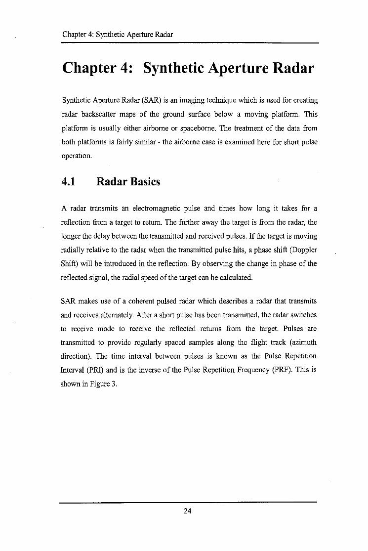
SAR makes use of a coherent pulsed radar which describes a radar that transmits
and receives alternately. After a short pulse has been transmitted, the radar switches
to receive mode to receive the reflected returns from the target. Pulses are
transmitted to provide regularly spaced samples along the flight track (azimuth
direction). The time interval between pulses is known as the Pulse Repetition
Interval (PRI) and is the inverse of the Pulse Repetition Frequency (PRF). This is
shown in Figure 3.
24
Chapter 4: Synthetic Aperture Radar
• • • • • • • • • :5 ••••••••• :l E
~ ·r ...... . PRI = 1/PRF
• • • • • • • • • Range
Figure 3: Radar Timing Relationships
Current radars are, for the most part, digital systems. When the radar begins
receiving the reflections from its transmission, I Q demodulation is performed
followed by an analogue to digital conversion. Complex sampling is used so that
the phase information of the signal is not lost. For strip-mapping SAR, the sampling
always starts a fixed time after the transmission ends. This is important as it allows
each sample to represent a particular range bin. Each range bin has a corresponding
ground resolution. Thus the returns from a stationary target (relative to the radar)
will always appear in the same range bin.
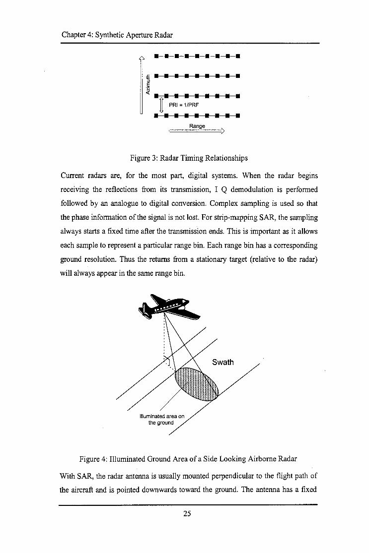
Figure 4: Illuminated Ground Area of a Side Looking Airborne Radar
With SAR, the radar antenna is usually mounted perpendicular to the flight path of
the aircraft and is pointed downwards toward the ground. The antenna has a fixed
25

Chapter 4: Synthetic Aperture Radar
beamwidth and so an oval shaped footprint is illuminated by the radar. In this way,
as the aircraft flies along its flight path, the radar will illuminate a swath on the
ground (see Figure 4). As the azimuth beamwidth is fairly large, a target is
illuminated a number of times by successive transmission pulses as it travels
through the beamwidth of the antenna. If the target is stationary on the ground, as
the aircraft flies past it, the distance to the target will change. If the distance to the
target were plotted, it would be hyperbolic as shown in the top block of Figure 5.
This is known as range migration.
4.2 SAR Processing
4.2.1 Overview
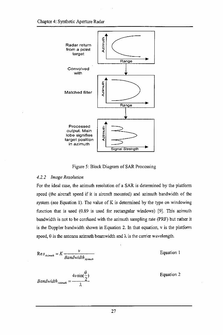
Since the target is illuminated multiple times, the resulting image needs to be
"focussed" so that the exact position of the target can be identified. Convolving
with a matched filter for the target achieves this. The matched filter is constructed
by simulating the return from a single point target and taking the time reversed,
complex conjugate of it. The filter is applied in azimuth (the direction of flight of
the aircraft).
The matched filter is then convolved with the returned data. Once the matched filter
has been applied, the image is said to be focussed. The position of individual targets
in azimuth can now be identified by locating peaks in the focussed data. A block
diagram of the processing can be seen in Figure 5.
26
Chapter 4: Synthetic Aperture Radar
Radar return from a point
target
Convolved with
Matched filter
Processed output. Main lobe signifies
target position in azimuth
~ .... :::l E ~
~ .... :::l E ~
Range
Range
Signal Strength
Figure 5: Block Diagram of SAR Processing
4.2.2 Image Resolution
For the ideal case, the azimuth resolution of a SAR is determined by the platform
speed (the aircraft speed if it is aircraft mounted) and azimuth bandwidth of the
system (see Equation 1). The value of K is determined by the type on windowing
function that is used (0.89 is used for rectangular windows) [9]. This azimuth
bandwidth is not to be confused with the azimuth sampling rate (PRF) but rather it
is the Doppler bandwidth shown in Equation 2. In that equation, v is the platform
speed, 8 is the antenna azimuth beamwidth and /...., is the carrier wavelength.
v Res Azimuth = K---. --
Bandwidth Azimuth
4vsin(~) Bandwidth Azimuth = 2
A.
Equation 1
Equation 2
27
Chapter 4: Synthetic Aperture Radar
Once the image has been focussed as described above, the power output of the
focussed returns around the area of the target appear similar to a sin( x) function, as x
seen in the bottom block of Figure 5. This sin(x) function is formed as the result of x
the inverse Fourier Transform of a Rect function since the frequency spectrum of
the transmitted wave, the received wave and the matched filter are all
approximately Rect functions.
Three measures often used with point targets to determine the quality of the
focussed image are: The width of the main peak, the peak sidelobe level and the
integrated sidelobe level. The width of the peak, taken at the -3dB points, is used to
calculate the actual azimuth resolution of the radar. The azimuth resolution is
calculated by multiplying the peak width (measured in number of samples) by the
sample size given by _v_ which is the ground spacing of the samples. During the PRF
convolution process, sidelobes are introduced into the output. These sidelobes
appear as ghost targets in the focussed image, regularly spaced from the main
target. The brightness of these ghost targets is related to the sidelobe level. It is
therefore necessary to minimise the sidelobes to prevent the introduction of ghost
images in the focussed image. A method of reducing them is to apply a window
function to the matched filter. This has the effect of widening the main peak but
also further reducing the sidelobes. Using a Hamming window will reduce the peak
sidelobe level to approximately -40dB, compared to a rectangular window which
provides sidelobe levels of approximately-13dB. A Hamming window will have a
window factor of 1.30 in Equation 1 [9].
The integrated sidelobe level gives a measure of how much of the radar energy
returns are in the sidelobes compared to the amount in the target return peak.
The resolution of a SAR in both range and azimuth is bandwidth limited. The
theoretical maximum azimuth resolution is given in Equation 1 while the theoretical
maximum range resolution is given in Equation 3. Note that there is also a window
factor incorporated here for the window function that is used in range compression.
28

Chapter 4: Synthetic Aperture Radar
A measure the effectiveness of the SAR processing and the quality of the radar can
be made by comparing the theoretical resolution of the radar with its measured
performance.
Re solution Range = K range ~ 2BandwzdthTx _pulse
Equation 3
29

Chapter 5: Preprocessor Design
Chapter 5: Preprocessor Design
5.1 Overview
This preprocessor was designed for the airborne SASAR 1 VHF (141MHz) Radar,
set to undergo flight testing in mid 1998. As the name implies, the SASAR Radar
was the South African Synthetic Aperture Radar. The radar sampled the return from
its transmission with a pair of analogue to digital converters. Before this digital data
could be stored, it had to be processed as the current data recorders could not record
at the required data rate when the radar sampled at 4096 range bins per PRI.
The processing requirements were therefore to reduce the data rate of the sampled
data, thus allowing the data recorders to store all the data. This processing was not
to contaminate the data in any way which could negatively affect any SAR
processing which would be performed at a later stage. This meant that the
processing could not introduce any phase shift into the data. It would however be
advantageous if the processing could improve the signal to noise ratio of the data.
The following table lists some of the important radar specifications:
Table 1: Radar Specifications
Pulse Repetition Frequency 625Hz Carrier Frequency 141MHz Pulse Width 88ns Max Range Resolution 13.2m Azimuth Beamwidth 45° Elevation Beamwidth 60° Aircraft Ground Speed 250m/sec Range samples per PRI (I,Q) 2048/4096 Maximum Doooler Bandwidth 180Hz
To lower the data rate, the effective pulse repetition frequency had to be reduced
since reducing the number of range samples per PRI would have reduced the
30
Chapter 5: Preprocessor Design
performance of the radar. When processing SAR images, it is often desirable to
make the azimuth and range resolution of the focussed image the same. The range
resolution of the SASAR system was approximately 13 meters. SAR processing
required that the azimuth bandwidth was approximately 37Hz to be able to focus
the image to approximately 13 meters in azimuth with 2 independent looks for
speckle reduction. Thus, the full 180Hz bandwidth which was available (see Table
1) was not required. The radar was sampling at a rate of 625Hz in azimuth. By
reducing the azimuth sampling rate (PRF), the data rate would be reduced. The PRF
could be reduced by a factor of 12 to give an effective PRF of 52Hz, slightly above
the required 37Hz processing bandwidth. Since complex sampling was used, the
Nyquist Sampling Rate was 37Hz.
The simplest method of reducing the azimuth sampling rate was to only store every
nth range line. Other methods existed which did not discard valuable data or result in
aliasing and these made use of a low pass filter. By low pass filtering the data, the
higher frequency components were removed. The signal could then safely be sub
sampled without infringing the Nyquist Sampling Criterion.
5.2 Current System
The current system made use of a presummer. The process of presumming involved
calculating the average of a number of PRis, thus implementing a crude low pass
filter. Consecutive range lines were added to produce a single range line output.
This adding took place in azimuth i.e. the corresponding range bins in each PRI
were added. If a presummer of factor five were used then five range lines would be
added to give one range line output. Presumming the data would have increased the
signal to noise ratio as the noncoherent noise would have been added together and
cancelled itself while the coherent signal would not.
Before considering alternative solutions, modifications to the current system were
considered. The only possible modification was to increase the presum factor to the
required value of 12. This would have reduced the data rate and increased the signal
to noise ratio as a number of PRis would be summed to give the filter output. The
31
... ,_ ,·r·---:~ ,. ........ ;."
Chapter 5: Preprocessor Design
noncoherent noise would therefore sum to zero and only the signal would remain.
The problem with method was that the Nyquist Sampling Criterion was infringed
by doing this as the data contained frequency components of 180Hz, as given by the
Maximum Doppler Bandwidth in Table 1. For this reason, other solutions had to be
investigated.
5.3 Proposed Solutions
Two methods of filtering were examined. The first involved a low pass filter with a
sampling frequency of 625Hz and a bandwidth of 20Hz while the second method
was a combination of a presummer and a filter. Both these methods were tested as
described in Section 5.5.1.
5.3.1 Filtering with no Presummer
This method required that a low pass filter be applied to the data in the azimuth
direction. The low pass filtering would null the frequency components which were
higher than approximately 20Hz 3. This would constrain the bandwidth of the signal
to approximately 40Hz so the data could safely be subsampled at 52Hz. The signal
to noise ratio would be increased since the returns from many PRis would be
combined to form a single output.
5.3.2 Filtering after Presumming
A combination the current system design and the method described above was also
possible. In this method, a presummer would be used to reduce the PRF to a value
just higher than the Doppler Bandwidth of the system. This would be achieved by
presumming the data by a factor of three and would reduce the effective PRF to
208.33Hz. A presum factor of three was the largest that could be used without
infringing the Nyquist Sampling Criterion since the bandwidth of the signal was
180Hz. A low pass filter could then be used to remove the high frequency
components of the signal before it was subsampled at 52Hz. The advantage of this
3 The filter is obviously not a brick wall filter and so some higher frequency components will be passed. The attenuation in the stop band is finite so the higher frequencies will still be present although at a greatly reduced
level.
32
Chapter 5: Preprocessor Design
method was that a filter with a steeper cutoff could be achieved with a fewer
number of taps.
5.4 Filter Design
Digital filters were available in two flavours: Finite Impulse Response (FIR) and
Infinite Impulse Response (IIR). The former was the easier of the two to implement
as it simply consisted of a tapped delay line where each tap is multiplied by a
scaling factor. More importantly, the filter required a linear phase response so that it
did not adversely affect the SAR processing of the data - a process that relied on
accurate phase measurements. Symmetric FIR filters with real coefficients have this
characteristic [12].
The design of a FIR filter was centred around the sampling frequency of the data it
operated on. Operating the same filter on data with different sampling rates
produced different filter characteristics.
FIR filters are defined by a number of characteristics including the number of filter
taps, their corresponding coefficients and the amount of ripple in the passband. The
relationship between the filter coefficients and the frequency response of the filter
can be seen in Equation 4 [12], where Hd is the ideal frequency response of the filter
and n is the sample number. This implies that an infinite length filter is required to
accurately describe the frequency response of a filter. The number of taps used
affects the accuracy of the frequency response of the filter; the longer the filter, the
more accurate the representation.
Equation 4
There are a number of methods for calculating the filter coefficients and these are
usually performed by computer. Two filter design packages were used: Matlab and
QED (a part of the COSSAP package written by Synopsys
http://www.svnopsys.com). Matlab source code was provided in [16]. The design of
filters is beyond the scope of this document but it is sufficient to mention that there
33
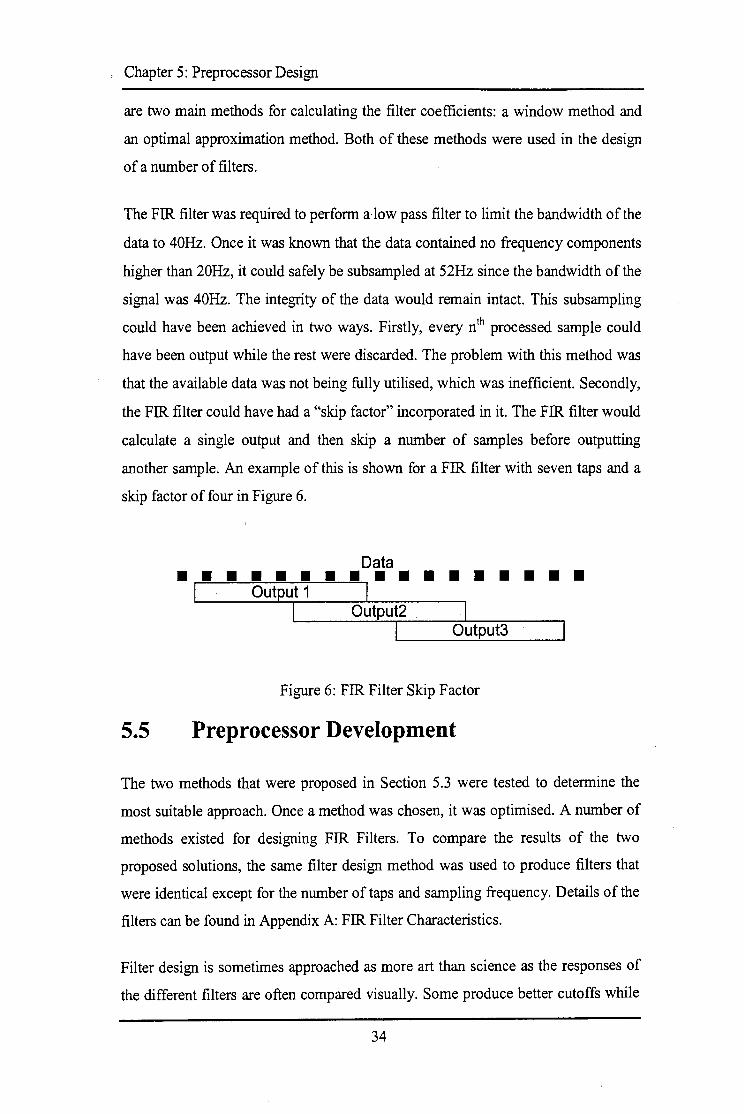
, Chapter 5: Preprocessor Design
are two main methods for calculating the filter coefficients: a window method and
an optimal approximation method. Both of these methods were used in the design
of a number of filters.
The FIR filter was required to perform a low pass filter to limit the bandwidth of the
data to 40Hz. Once it was known that the data contained no frequency components
higher than 20Hz, it could safely be subsampled at 52Hz since the bandwidth of the
signal was 40Hz. The integrity of the data would remain intact. This subsampling
could have been achieved in two ways. Firstly, every n1h processed sample could
have been output while the rest were discarded. The problem with this method was
that the available data was not being fully utilised, which was inefficient. Secondly,
the FIR filter could have had a "skip factor" incorporated in it. The FIR filter would
calculate a single output and then skip a number of samples before outputting
another sample. An example of this is shown for a FIR filter with seven taps and a
skip factor of four in Figure 6.
• • • • • • • I Output 1
Data • • • I Output2
• • • • • • • Output3
Figure 6: FIR Filter Skip Factor
5.5 Preprocessor Development
The two methods that were proposed in Section 5.3 were tested to determine the
most suitable approach. Once a method was chosen, it was optimised. A number of
methods existed for designing FIR Filters. To compare the results of the two
proposed solutions, the same filter design method was used to produce filters that
were identical except for the number of taps and sampling frequency. Details of the
filters can be found in Appendix A: FIR Filter Characteristics.
Filter design is sometimes approached as more art than science as the responses of
the different filters are often compared visually. Some produce better cutoffs while
34
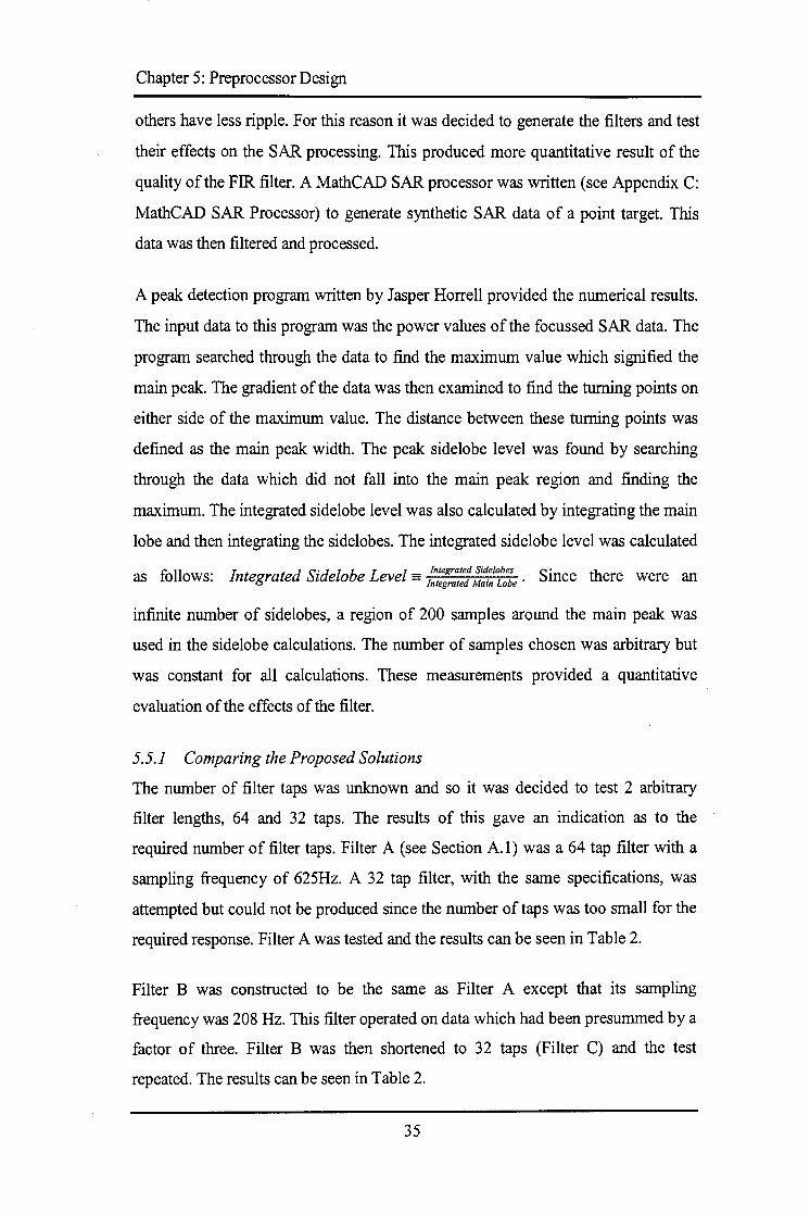
Chapter 5: Preprocessor Design
others have less ripple. For this reason it was decided to generate the filters and test
their effects on the SAR processing. This produced more quantitative result of the
quality of the FIR filter. A MathCAD SAR processor was written (see Appendix C:
MathCAD SAR Processor) to generate synthetic SAR data of a point target. This
data was then filtered and processed.
A peak detection program written by Jasper Horrell provided the numerical results.
The input data to this program was the power values of the focussed SAR data. The
program searched through the data to find the maximum value which signified the
main peak. The gradient of the data was then examined to find the turning points on
either side of the maximum value. The distance between these turning points was
defined as the main peak width. The peak sidelobe level was found by searching
through the data which did not fall into the main peak region and finding the
maximum. The integrated sidelobe level was also calculated by integrating the main
lobe and then integrating the sidelobes. The integrated sidelobe level was calculated
as follows: Integrated Sidelobe Level = fn::e;,~~d :/,,~:'~~~e . Since there were an
infinite number of sidelobes, a region of 200 samples around the main peak was
used in the sidelobe calculations. The number of samples chosen was arbitrary but
was constant for all calculations. These measurements provided a quantitative
evaluation of the effects of the filter.
5. 5.1 Comparing the Proposed Solutions
The number of filter taps was unknown and so it was decided to test 2 arbitrary
filter lengths, 64 and 32 taps. The results of this gave an indication as to the
required number of filter taps. Filter A (see Section A. I) was a 64 tap filter with a
sampling frequency of 625Hz. A 32 tap filter, with the same specifications, was
attempted but could not be produced since the number of taps was too small for the
required response. Filter A was tested and the results can be seen in Table 2.
Filter B was constructed to be the same as Filter A except that its sampling
frequency was 208 Hz. This filter operated on data which had been presummed by a
factor of three. Filter B was then shortened to 32 taps (Filter C) and the test
repeated. The results can be seen in Table 2.
35

Chapter 5: Preprocessor Design
The expected results were obtained. Filter A performed the worst as the azimuth
resolution obtained was less than half of the filters. The reason for this can be
attributed to the very wide passband, as can be seen in Figure 29. This introduced
aliasing as the filter cutoff frequency was higher than the new sampling frequency
of 52 Hz. It was expected that the longer filter would produce better results. This
was partly true in that the longer filter produced a finer azimuth resolution. What
was interesting was that the shorter filter (Filter C) had lower sidelobes than Filter
B. The reason for this is unclear and is an area that requires further investigation.
The difference between filters B and C was negligible in terms of resolution. Since
an azimuth resolution of six meters was required, it was decided to use a 32 tap
filter as that would ease processing requirements.
Table 2: Initial Test Filter Performance
Name No.of Sampling Azimuth Peak Integrated Taps Frequency Resolution Sidelobe Sidelobe Level
Level Filter A 64 625Hz 11.064 m -12.619 dB -18.411 dB Filter B 64 208Hz 5.268 m -13.749 dB -11.513 dB Filter C 32 208Hz 5.352 m -14.840 dB -13.347 dB
5.5.2 Finding the Optimal Filter
The solution to be implemented had been decided upon and was then optimised. A
number of different filters were calculated and tested to find one which provided the
optimal effects on the SAR processing. Besides Filter C which had already been
tested, three further filters were designed. All three had the same specifications (32
taps, 40 Hz bandwidth) except that the method used to calculate their coefficients
was different. A comparison of their frequency responses can be seen in Figure 7.
The characteristics of the filters can be seen in Appendix A: FIR Filter
Characteristics while the results of the testing can be seen in Table 3.
36

-------------------~----------------------~ r
Chapter 5: Preprocessor Design
Table 3: Final Filter Performance
Name No. of Taps
Filter D 32 Filter E 32 Filter F 32
Design Method
Kaiser Equiripple
Linear
Azimuth Resolution
5.196 m 4.932 m 5.208m
Peak Sidelobe
Level -14.276 dB -14.590 dB -15.174 dB
Integrated Sidelobe Level
-12.070 dB -12.452 dB -12.015 dB
It was noted in the processed outputs that aliasing had been introduced. Upon
further investigation it appeared that this was introduced by the FIR filter when
subsampling took place. The reason for this was that the stop band of the FIR filters
would only attenuate the signal by approximately 20dB. This can be seen in Figure
35, Figure 37 and Figure 39. Frequency components which were higher than the
Nyquist Sampling Frequency were therefore still present in the signal and these
introduced the aliasing. The level of the aliased level (see Figure 8) was
approximately 20dB lower than the focussed peak (seen in the centre of the
diagram).
Filter F was chosen as the filter to be implemented. The reason for this was that it
produced the lowest sidelobe level, as can be seen in Table 3. Although the azimuth
resolution was worse than Filters D and E, this was not a problem as the final image
would only be focussed to approximately 13m (see Section 5.1).
37
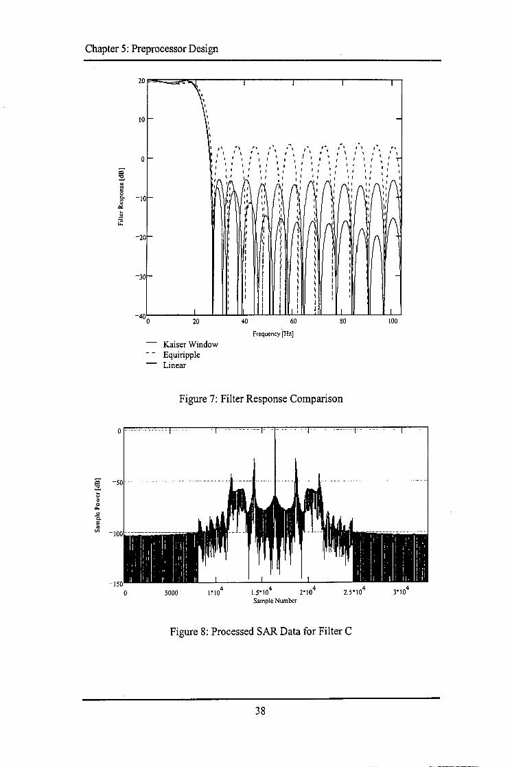
Chapter 5: Preprocessor Design
IO
0
;:ii' ~ i;l
" 0
~ -10 " ~ -~ ~
-20
0 -
-100
-150 0
I ,1 I I
I
'•
20
Kaiser Window Equiripple Linear
I
., ' ' I ' I '
I I
I I
40
.. " ' ' '~ '' I \ I 'I I
I I I I f " •' . ~ . , .
I I r • , , r ' I I
I I I
I I I I
60 80 100
Frequency [Hz]
Figure 7: Filter Response Comparison
5000 2.5· 104
Sample Number
Figure 8: Processed SAR Data for Filter C
38
Chapter 5: Preprocessor Design
5.6 Algorithm Model
Once the details of the presumrner and filter were decided upon, a VHDL algorithm
model was written to test the effects of quantisation and precision. The MathCAD
simulation made use of floating point values which were not available in FPGAs.
The algorithm model had to provide a means for testing the precision needed when
storing intermediate results as well the bit growth encountered when presumrning
and filtering.
Before the model could be written, the expected bit widths of the data at various
stages in the processing had to be calculated. The presummer operated on eight bit
values and presumrned three of them for each result. Adding 3 eight bit numbers
resulted in a ten bit number if no precision was to be lost. The presummer output
was therefore set at ten bits per value. The bit growth in the FIR filter could be
calculated as follows: The data to be operated on was ten bits wide. The coefficients
were each eight bits wide. Thus every multiplication in the FIR filter produces an
18 bit result. There were 32 taps so 32 eighteen bit numbers were to be added. This
would produce a 23 bit result. The internal precision of the FIR filter was therefore
set at 23 bits. The data path widths can be seen in Figure 9.
The required output eight bits wide so the FIR filter output had to be divided to
produce this. The division ratio was the presum gain (3) multiplied by the FIR filter
gain (952). This produced the final eight bit value.
The VHDL algorithm model was written to read and write its data from disk. The
output data would be used to test the results of the other models that were written. A
model of the presumrner was first coded and its output was manually verified. This
data was then used as input to the prefilter model and once again the results were
manually verified. Manual verification involved calculating the expected output and
comparing it with the output produced by the model.
To test the effects of quantisation, the synthetic data which was generated in the
MathCAD SAR processor was quantised to eight bits and processed by the
algorithm model. This data was then imported back into the MathCAD processor
39
. --·-·---·-·· ,,_,_,_,,_,.,, ~ ............ -·· ,,.,, ..... ,,.v.,, -·······.· ·- ..... .

Chapter 5: Preprocessor Design
and the image was focussed. The effects of quantisation were seen when comparing
the outputs from the MathCAD and VHDL simulations, although the differences
were minor. The peak sidelobe level of the MathCAD simulation was -14.279 dB,
compared with the VHDL simulation value of -14.230 dB, while the integrated
sidelobe level of the MathCAD simulation was -12.072 dB, compared with -12.033
dB. The width of the peak of the focussed target also increased by 0.23%. In a
focussed image, these differences would not be noticeable to the naked eye. The
reason why the quantisation effects in the final image were small was due to the
large integration of the SAR processing.
DC Offset: 128 Output Data Width: 8 bits Output Data Type: signed
Data In~----. DC Offset Removal
PRF: 625 Hz No Samples/ PRI : 4096 Data Format: 8 bits Data Type: unsigned
Number of Taps : 32 Tap Coefficient Width: 8 bits Input Data Width: 10 bits Output Data Width: 23 bits
Presummer FIR Filter
Presum Factor: 3 Input Data Width: 10 bits Output Data Width: 10 bits
DC Offset: 128 Output Data Width: 8 bits Output Data Type: unsigned
Divider
~-----=;Data Out DCOffset ~ Insertion '-----V
Divide Ratio: 2856 Input Data Width: 23 bits Output Data Width: 8 bits
Figure 9: Algorithm Model Block Diagram
40

••
Chapter 6: Hardware Design
Chapter 6: Hardware Design
The preprocessor described above in Chapter 5: Preprocessor Design had to be
implemented in hardware. Part of the objective of this thesis was to investigate the
level of complexity of signal processing that could be achieved in dedicated
hardware i.e. without the use of general purpose digital signal processors.
The simplest method of obtaining customised hardware was to make use of Field
Programmable Gate Arrays (FPGAs). These devices contained thousands of digital
logic gates that could be interconnected at will. Design software for these devices
was used to produce a configuration file that could then be downloaded to the
FPGA. This configuration file specified how these gates were to be connected.
6.1 Hardware Requirements
Before any hardware could be specified, the some basic calculations had to be
performed to determine the input and output data rates and the amount of data to be
stored. Since complex sampling was used, the I and Q values could be treated
separately. This allowed a system to be designed to handle just the I values which
could then be duplicated to handle the Q values. The following calculations are
therefore only for the I values and are the same as those for the Q values.
For the presummer, one range line containing 4096 samples arrived every PRI. One
PRI took l.6ms (1/625 Hz) and so each sample had to be completed in 390ns. For
the prefilter, since there was a skip factor of 4, a range line had to be output after 12
PRis which took 19.2ms. Thus each prefiltered sample had to be completed in 4.6us
(19.2ms/4096).
The calculations above gave the basic timing constraints of the system. Lower level
timing could not be done at that time as such timing was dependent on the routing
delays within the FPGA. To presum one sample, the sample had to be read from
memory, added to another sample and the result then written back to memory.
41

Chapter 6: Hardware Design
Performing such an operation in 390ns seemed possible4, considering that RAM
access times were of the order of tens of nanoseconds and additions were of the
same order. Similarly for each prefiltered sample, 32 RAM reads had to be
performed as well as 32 multiply and adds. It therefore seemed, at a first look, as
though these operations were possible in the allocated time.
Since the timing of each hardware operation was not accurately known, the
possibility existed that the hardware would not be fast enough to meet the
requirements above. To cope with this, methods were investigated to speed up the
processing. These are detailed in Section 6.3.
6.2 Memory Overview
From the design detailed in Chapter 5: Preprocessor Design, it was decided to use a
presummer before the prefilter. For the purposes of design, the prefilter and
presummer were treated separately as they were mathematically separate. They
could always be combined into a single FPGA at a later stage. I
Both the presummer and prefilter needed RAM in which to store data. The
presummer had to store the cumulative result of the presumming process before the
final result was available. The prefilter had to store all the incoming data to be able
to filter it as the data was to be filtered in azimuth, not range. Hence for a 32 tap
filter, al least 32 range lines would need to be stored for each output row to be
calculated.
The interface between the presummer and prefilter had to be determined. Two
methods were evaluated. The first involved the use of separate memories for the
prefilter and presummer while the second method used shared memory. The latter
option was implemented.
4 When the final implementation of the presurnrner was verified, it was able to perform at the required speed.
42
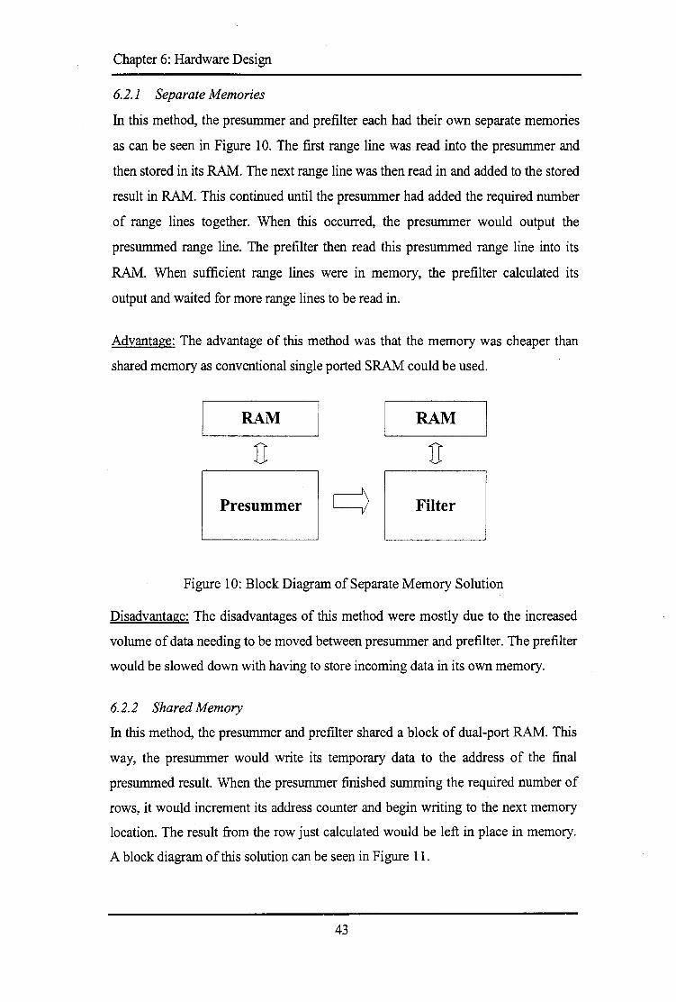
Chapter 6: Hardware Design
6.2.1 Separate Memories
In this method, the presummer and prefilter each had their own separate memories
as can be seen in Figure 10. The first range line was read into the presummer and
then stored in its RAM. The next range line was then read in and added to the stored
result in RAM. This continued until the presummer had added the required number
of range lines together. When this occurred, the presummer would output the
presummed range line. The prefilter then read this presummed range line into its
RAM. When sufficient range lines were in memory, the prefilter calculated its
output and waited for more range lines to be read in.
Advantage: The advantage of this method was that the memory was cheaper than
shared memory as conventional single ported SRAM could be used.
RAM RAM
Presummer Filter
Figure 10: Block Diagram of Separate Memory Solution
Disadvantage: The disadvantages of this method were mostly due to the increased
volume of data needing to be moved between presummer and prefilter. The prefilter
would be slowed down with having to store incoming data in its own memory.
6.2.2 Shared Memory
In this method, the presummer and prefilter shared a block of dual-port RAM. This
way, the presummer would write its temporary data to the address of the final
presummed result. When the presummer finished summing the required number of
rows, it would increment its address counter and begin writing to the next memory
location. The result from the row just calculated would be left in place in memory.
A block diagram of this solution can be seen in Figure 11.
43
... ·-- .. ·~·"-:.~- '· .
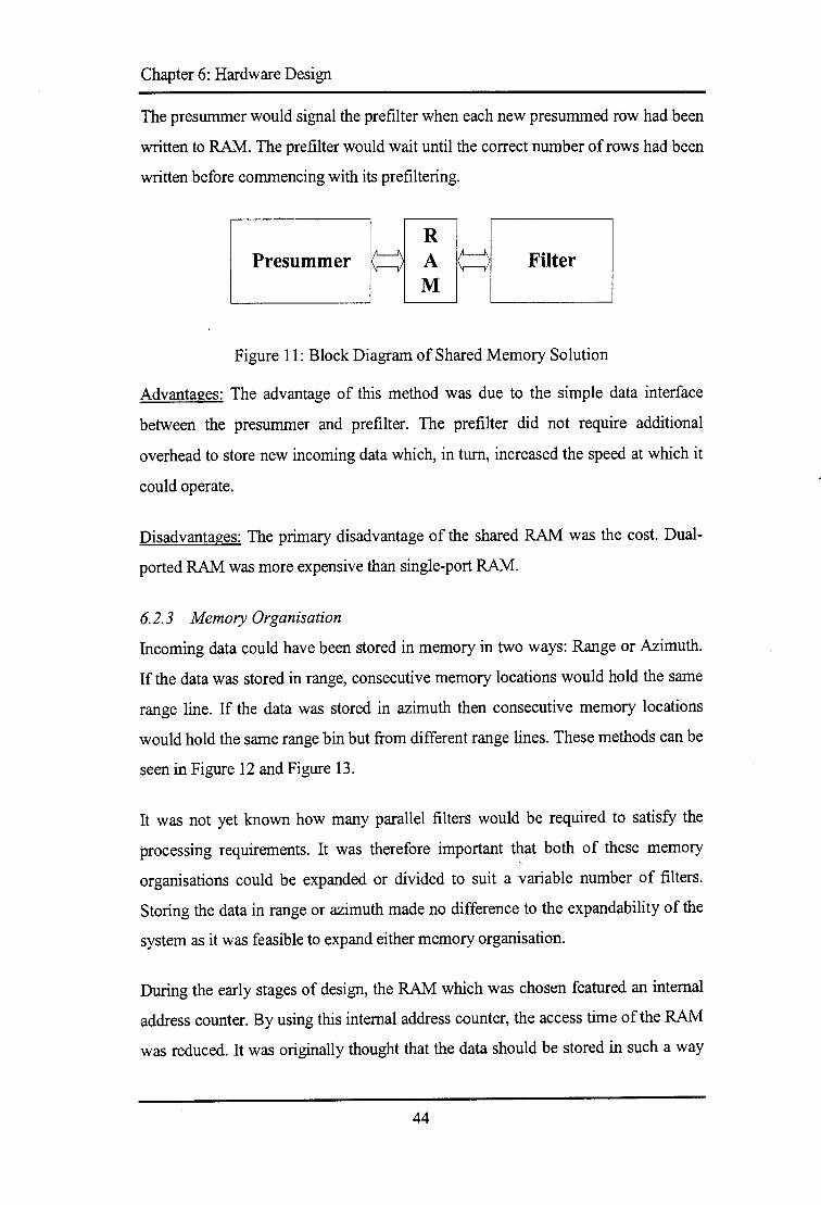
Chapter 6: Hardware Design
The presummer would signal the prefilter when each new presummed row had been
written to RAM. The prefilter would wait until the correct number of rows had been
written before commencing with its prefiltering.
Presummer 9 ~ lh'------F-i-lt-er----'
Figure 11: Block Diagram of Shared Memory Solution
Advantages: The advantage of this method was due to the simple data interface
between the presummer and prefilter. The prefilter did not require additional
overhead to store new incoming data which, in turn, increased the speed at which it
could operate.
Disadvantages: The primary disadvantage of the shared RAM was the cost. Dual
ported RAM was more expensive than single-port RAM.
6.2.3 Memory Organisation
Incoming data could have been stored in memory in two ways: Range or Azimuth.
If the data was stored in range, consecutive memory locations would hold the same
range line. If the data was stored in azimuth then consecutive memory locations
would hold the same range bin but from different range lines. These methods can be
seen in Figure 12 and Figure 13.
It was not yet known how many parallel filters would be required to satisfy the
processing requirements. It was therefore important that both of these memory
organisations could be expanded or divided to suit a variable number of filters.
Storing the data in range or azimuth made no difference to the expandability of the
system as it was feasible to expand either memory organisation.
During the early stages of design, the RAM which was chosen featured an internal
address counter. By using this internal address counter, the access time of the RAM
was reduced. It was originally thought that the data should be stored in such a way
44
'., ...... ···-~~'----'-· ._,. ;_.'""-"-.:·_·"~:·:·_ ... .:...;''';___'' ,,_. '.;;..." .. _ .... _.... '-'----------'·-.··.: ....... _...._. _____ ._. -· _ .. -··•..,·.-.-·':"-····-· -· -----· _ ..... , .• _ ... ,_ .. ',.;,';;-·: .,,.;,,;,.;,· iii" ............. _.-.... ·:·;-0.-.... -., •• ,._ .. -""
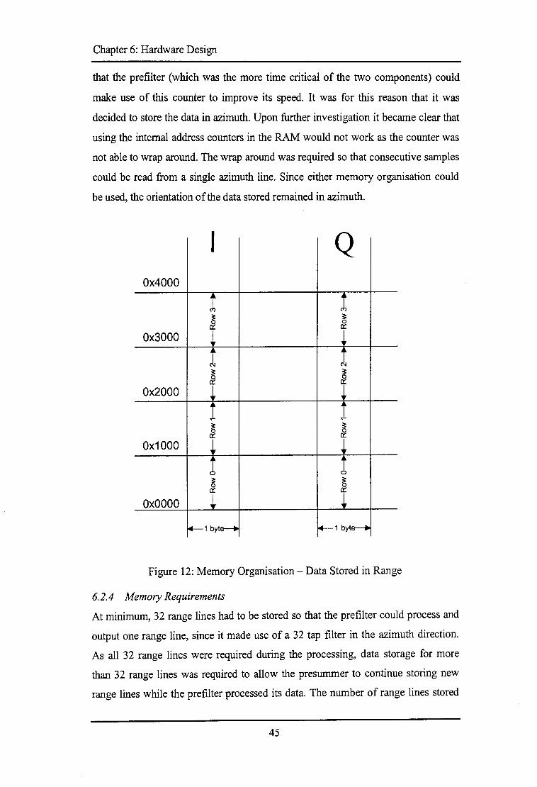
Chapter 6: Hardware Design
that the prefilter (which was the more time critical of the two components) could
make use of this counter to improve its speed. It was for this reason that it was
decided to store the data in azimuth. Upon further investigation it became clear that
using the internal address counters in the RAM would not work as the counter was
not able to wrap around. The wrap around was required so that consecutive samples
could be read from a single azimuth line. Since either memory organisation could
be used, the orientation of the data stored remained in azimuth.
I Q Ox4000
1 1 ~
;:: 0 a::
Ox3000 ,. ' N N ;:: ~ 0 a:: a::
Ox2000 ,
' ...... ......
~ ;:: 0 a:: a::
Ox1000 r Ir
·~ ' :i ':> ;:: ;:: 0 0
OxOOOO l l ~1byt~ i.--1 byt~
Figure 12: Memory Organisation-Data Stored in Range
6.2.4 Memory Requirements
At minimum, 32 range lines had to be stored so that the prefilter could process and
output one range line, since it made use of a 32 tap filter in the azimuth direction.
As all 32 range lines were required during the processing, data storage for more
than 32 range lines was required to allow the presummer to continue storing new
range lines while the prefilter processed its data. The number of range lines stored
45

Chapter 6: Hardware Design
was required to be a power of 2 since that would allow address counters to roll over
at the correct values. This was necessary as only a set number of PRis could be
stored and there was no limit on the number of incoming range lines. It was decided
that storage space for 64 range lines would be made available since that was the
next possible value after 32.
The width of the data memory was also considered. The incoming data from the
radar was 8 bits wide. Adding three 8 bit numbers resulted in a 10 bit number,
assuming an overflow was not allowed. It was therefore decided that 10 bit memory
was to be used. This prevented the loss of any dynamic range due to overflow.
The total amount of RAM required was 512K x 10 bits. This number was decided
upon as follows: 64 PRis, each of 4096 complex samples = 64 * 4096 * 2 = 512K.
I Q Ox0100
! l c: c: iii iii
OxOOCO • .. ... ' N N c: c: iii iii
Ox0080 '
... ... c: c: iii iii
Ox0040 . ' . .. c:> ')
OxOOOO ! ! i.--1 byte-}I 14-1 byte-}I
Figure 13: Memory Organisation - Data Stored in Azimuth
46
: . :· .. :-.7~·--... -.~,_,., .. ,
Chapter 6: Hardware Design
6.2.5 Memory Selection
Two types of Dual Ported RAM were available at design time: Synchronous and
Asynchronous. The latter was the more common variety. To generate the precise
timing signals required to access asynchronous RAM from an FPGA usually
required the use of external programmable delay lines, unless multiple clock cycles
were to be used to generate the required waveforms. These delay lines added extra
complexity to the circuit, as well as an increased chip count.
Since synchronous design was the preferred approach m FPGA design,
synchronous RAM was considered as an alternative. It appeared that synchronous
RAM could be interfaced directly to the FPGA and still provide single clock cycle
accesses. Further investigation took place to determine which devices were
available.
In an attempt to minimise the chip count, high capacity RAM chips were sought.
Cypress Semiconductor were going to produce a device which suited the needs of
the radar. This was their CY7C09099 which was available in 128Kx8. It appeared
at the time that the minimum width of available devices was 8 bits. This
necessitated using two devices in parallel to achieve the required 10 bit data bus
width. Wasting the 6 bits was unavoidable. At design time, this device was
sampling and should have been available at the end of 1998.
6.2.6 VHDL Memory Model
Once the decision to use this device was made, the author attempted to locate a
VHDL model for it. This model would be used in the functional model as well as in
the simulation of the final FPGA. A suitable model could not be found and so it was
decided to write one.
The model was a functional model and therefore contained no timing information,
although this could have been added if required. The data for the model was
obtained from a preliminary data sheet, since the final data sheets were not
available.
47
Chapter 6: Hardware Design
The model differed from the data sheet in one area. The width of the data bus was
increased from 8 bits to 10 bits. The reason for doing this was purely to increase its
simulation performance. Even though the data was only 8 bits wide, each memory
location required 32 bits to store because the value was stored as an integer. By
increasing the model's data bus width to 10 bits, the memory required by RAM
simulation was halved. This also increased the speed at which the RAM simulated.
6.3 Hardware Expandability
As described in Section 6.1, the expandability of the system was critical to its
functioning, especially since the final operating speed of the hardware was not
known before it was designed.
The simplest method of improving speed was to use parallel processes. This applied
particularly to the FIR filters. Besides having two FIR filters (one for I values and
the other for Q values) it may have been necessary to have multiple parallel FIR
filters for processing the data. Since the filtering was done in azimuth, the data
could be split in range. For example ifthere were two I data filters, one could filter
the first half of the range bins while the other would filter the second half. Each
filter would then have twice the amount of time to process the data and so its
operating speed could be halved.
Both methods of memory organisation supported an increase in the number of
filters. Each filter would require its own memory from where it could read its input
data. The algorithm used by the presummer to calculate the position where the data
was stored would have had to be improved. This would have been simple with
memory mapping techniques.
A larger problem, should the system have required expansion, was to preserve the
position in the PRI of samples output from the different filters. The design of the
filters was to output their result for each range bin once it was processed. This
would obviously not have worked if more than one filter were writing output
samples at the same time. Samples from non-consecutive range bins could be output
at the same time, thus mixing their order in the range line. Two solutions were
48
- -- .• -- ......... ,. ................ ~ --- .. ·~--~--,.-,-·,,.·-_::-·: .. -;.·: ~""f""'~ .. ..-............ ,. ...... .
Chapter 6: Hardware Design
proposed although neither had to be implemented since the filters were fast enough
to process a complete range line I nthe required time.
6.3.1 Multiple Output FIFOs
This method made use of a FIFO for each filter coupled with some external control
hardware. Once the filter had processed its portion of a range line and written the
output data to its FIFO, it would have signalled the controller that it had completed
its portion of the range line processing. The controller would then have read the
contents of the FIFOs in the correct order and placed the processed data in a large
output FIFO. The data in this FIFO would then have been in the correct order, as
required.
Advantages: This method was the faster of the two in that the filters were required
only to filter the data. The filters performed no data movement besides that required
during the filtering.
Disadvantage: This method increased the chip count would therefore have been
more expensive to implement.
6.3.2 Writeback to RAM
In this method, the prefilter would have written the processed data back to the
RAM. Once the first filter had processed its portion of the range line, it would write
the processed data to the output FIFO. On completion, the filter would signal the
next filter to do the same. In this way, the data would be output in the correct order.
Advantage: This method was the cheaper solution as no extra ICs were required.
Disadvantages: This method was slower than using multiple FIFOs because the
filters had to write the processed data back to RAM when they could have been
reading new data. They would also have had to write the processed data to the
FIFOs during the time they could have been processing. This would have resulted
in a slower filter.
49
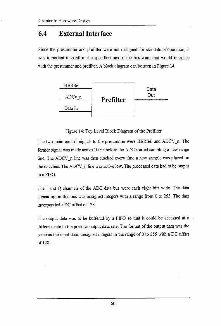
Chapter 6: Hardware Design
6.4 External Interface
Since the presummer and prefilter were not designed for standalone operation, it
was important to confirm the specifications of the hardware that would interface
with the presummer and prefilter. A block diagram can be seen in Figure 14.
HBRSel Data
ADCv n Out Pre filter
Data In
Figure 14: Top Level Block Diagram of the Prefilter
The two main control signals to the presummer were HBRSel and ADCV _ n. The
former signal was made active 1 OOns before the ADC started sampling a new range
line. The ADCV _ n line was then clocked every time a new sample was placed on
the data bus. The ADCV _n line was active low. The processed data had to be output
to a FIFO.
The I and Q channels of the ADC data bus were each eight bits wide. The data
appearing on this bus was unsigned integers with a range from 0 to 255. The data
incorporated a DC offset of 128.
The output data was to be buffered by a FIFO so that it could be accessed at a
different rate to the prefilter output data rate. The format of the output data was the
same as the input data: unsigned integers in the range of 0 to 255 with a DC offset
of 128.
50
............. ······· .... ··········-·······..-·--·.··················.-".'-""""''=···"-"···"="-:.;;;;:--·="·=····=····=·-··=·---· ...;,,;·-;;;...··;....· ="-'"""""-""""""'··.----·=·····= ........................... ,, ....... -----···--···.-.-····-··--· ---·-····-·····---------................. -.... -......... ..,. __ _
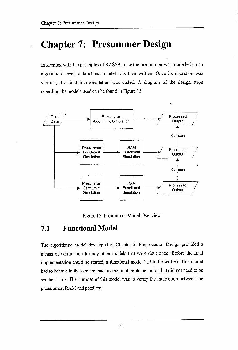
Chapter 7: Presummer Design
Chapter 7: Presummer Design
In keeping with the principles ofRASSP, once the presummer was modelled on an
algorithmic level, a functional model was then written. Once its operation was
verified, the final implementation was coded. A diagram of the design steps
regarding the models used can be found in Figure 15.
I Test / . Presummer ~ Processed I Data ... Algorithmic Simulation 7 Output
i Compare
I Presummer RAM Processed 7 ~ Functional . Functional ~ ... ...
7 Output Simulation Simulation
i Compare
I Presummer RAM Processed I ~ Gate Level
. Functional ~ ... ,,, 7 Output
Simulation Simulation
Figure 15: Presummer Model Overview
7 .1 Functional Model
The algorithmic model developed in Chapter 5: Preprocessor Design provided a
means of verification for any other models that were developed. Before the final
implementation could be started, a functional model had to be written. This model
had to behave in the same manner as the final implementation but did not need to be
synthesisable. The purpose of this model was to verify the interacti.on between the
presummer, RAM and prefilter.
51

Chapter 7: Presummer Design
7.1.1 Model Functionality
The VHDL model had to be able to interact with the RAM and FIFO models to be
able to perform a system level simulation. The model also had to perform a
presumming function of the incoming data. The only difference between this model
and the final implementation was that it could not be synthesised into a FPGA.
The functional model contained no routing delay timing. If an output changed logic
levels on a rising clock edge, that change would appear on the clock edge in the
model, unlike a real FPGA where it would only occur a few nanoseconds after the
clock edge. Another example of this lack of latency was in the addition and
multiplication operations. These occurred instantly in the model, unlike in a FPGA.
Since the entire design was synchronous, these did not present any problems as all
operations took place on a clock edge and didn't rely on the when in the previous
clock cycle the operation finished.
7.1.2 Presummer Interface
The first task during development of this model was to define the external interface.
A number of pins were required to allow the device to interface with the RAM,
external radar components and the prefilter. These pins are described in Table 4.
More detail on the FIFO and RAM pins can be obtained from the relevant data
sheets.
Table 4: Presummer Interface Pins
Pin Description FifoDatal, FifoDataQ FIFO Data Bus (I & Q Channels). These were
each 8 bits wide FifoWEnl_n, FifoWEn2 FIFO Write Enable. Both need to be active to
allow a write on the next rising edge of the FIFO
Write Clock.
FifoREnl_n, FifoREn2_n FIFO Read Enable. Both need to be active to allow a read on the next rising edge of the FIFO Read Clock
FifoEFI_n, FifoEFQ_n FIFO Empty Flags (I & Q Channels). These signals are active when the corresponding FIFO is empty.
FifoRs n FIFO Asynchronous Reset
52
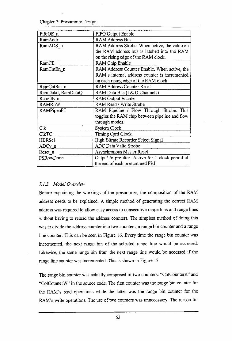
Chapter 7: Presummer Design
FifoOE n FIFO Output Enable RamAddr RAM Address Bus RamADS n RAM Address Strobe. When active, the value on
the RAM address bus is latched into the RAM on the rising edge of the RAM clock.
Ram CE RAM Chip Enable RamCntEn n RAM Address Counter Enable. When active, the
RAM's internal address counter is incremented on each rising edge of the RAM clock.
RamCntRst n RAM Address Counter Reset RamDataI, RamDataO RAM Data Bus (I & 0 Channels) RamOE n RAM Output Enable RAMRnW RAM Read I Write Strobe RAMPipenFT RAM Pipeline I Flow Through Strobe. This
toggles the RAM chip between pipeline and flow through modes.
Clk System Clock ClkTC Timing Card Clock. HBRSel High Bitrate Recorder Sdect Simal ADCv n ADC Data Valid Strobe Reset n Asynchronous Master Reset PSRowDone Output to prefilter. Active for 1 clock period at
the end of each presummed PRI.
7.1.3 Model Overview
Before explaining the workings of the presummer, the composition of the RAM
address needs to be explained. A simple method of generating the correct RAM
address was required to allow easy access to consecutive range bins and range lines
without having to reload the address counters. The simplest method of doing this
was to divide the address counter into two counters, a range bin counter and a range
line counter. This can be seen in Figure 16. Every time the range bin counter was
incremented, the next range bin of the selected range line would be accessed.
Likewise, the same range bin from the next range line would be accessed if the
range line counter was incremented. This is shown in Figure 17.
The range bin counter was actually comprised of two counters: "ColCounterR" and
"ColCounterW" in the source code. The first counter was the range bin counter for
the RAM's read operations while the latter was the range bin counter for the
RAM's write operations. The use of two counters was unnecessary. The reason for
53
: .... ·- ., •. ·:· .......... :· ... :" ... -::; ... :; ........ - ·""' ••• " ., •. : .7::-::::-".'.':~·::··- ........ 7.-.,:--.~ .. ,. •: .... .............. , ....... ~ ... - ................ ..
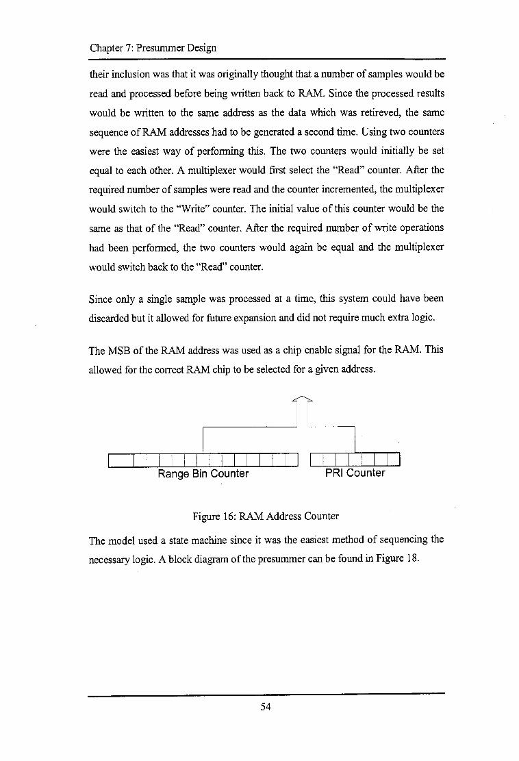
Chapter 7: Presumrner Design
their inclusion was that it was originally thought that a number of samples would be
read and processed before being written back to RAM. Since the processed results
would be written to the same address as the data which was retireved, the same
sequence of RAM addresses had to be generated a second time. Using two counters
were the easiest way of performing this. The two counters would initially be set
equal to each other. A multiplexer would first select the "Read" counter. After the
required number of samples were read and the counter incremented, the multiplexer
would switch to the "Write" counter. The initial value of this counter would be the
same as that of the "Read" counter. After the required number of write operations
had been performed, the two counters would again be equal and the multiplexer
would switch back to the "Read" counter.
Since only a single sample was processed at a time, this system could have been
discarded but it allowed for future expansion and did not require much extra logic.
The MSB of the RAM address was used as a chip enable signal for the RAM. This
allowed for the correct RAM chip to be selected for a given address.
I I I I I I i I I I I I I I I
Range Bin Counter I I I I I I I I
PRI Counter
Figure 16: RAM Address Counter
The model used a state machine since it was the easiest method of sequencing the
necessary logic. A block diagram of the presumrner can be found in Figure 18.
54
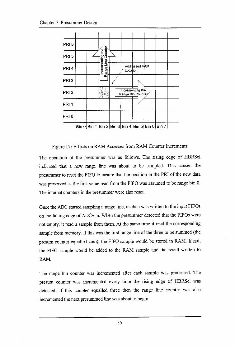
Chapter 7: Presummer Design
PRl6 !~
PRI 5 L_ ;g ~ c: (.)
:.;:::; Q) c: c: Q) ·-
PRl4 E .....! Addr ~ssed F AM Q) Q)
ts Cl / Loca ion c: c: I - Cll c::: ,I PRI 3 -
~ PRI 2 ~,·~f ~;.~ I
Incrementing th;> Range Bin Counte
PRI 1 v PRI 0
Bin 0 Bin 1 Bin 2 Bin 3 Bin 4 Bin 5 Bin 6 Bin 7
Figure 17: Effects on RAM Accesses from RAM Counter Increments
The operation of the presummer was as follows. The rising edge of HBRSel
indicated that a new range line was about to be sampled. This caused the
presummer to reset the FIFO to ensure that the position in the PRI of the new data
was preserved as the first value read from the FIFO was assumed to be range bin 0.
The internal counters in the presummer were also reset.
Once the ADC started sampling a range line, its data was written to the input FIFOs
on the falling edge of ADCv _n. When the presummer detected that the FIFOs were
not empty, it read a sample from them. At the same time it read the corresponding
sample from memory. If this was the first range line of the three to be summed (the
presum counter equalled zero), the FIFO sample would be stored in RAM. If not,
the FIFO sample would be added to the RAM sample and the result written to
RAM.
The range bin counter was incremented after each sample was processed. The
presum counter was incremented every time the rising edge of HBRSel was
detected. If this counter equalled three then the range line counter was also
incremented the next presummed line was about to begin.
55
Chapter 7: Presummer Design
State Machine Select Multiplexer
Range Bin Counter (Read)
Range Bin Counter (Write)
Ram ddress
PRI Counter
r-------lncremen>--------'
FIFO Data
HBRSe
Ram Data
= 2?
Presum Row Counter
Adder
= O? Sele
Figure 18: Block Diagram of Presummer
7.1.4 State Machine
Ram Data
Multiplexer
"O"
A state machine was written to control the presummer. This was done as it was the
simplest way of providing the required sequencing of operations. A block diagram
of the state machine can be seen in Figure 19. A description of the states follows
below.
StateReset: This was the reset state. It cleared all the counters, reset the FIFOs and
the RAM signals.
Stateldle: This was the idle state. The state machine remained in this state while
there are no samples in the FIFO.
StateRead: This was the read state. In this state, data was read from the FIFO and
the RAM. The registers for holding this data were enabled to allow the data to be
stored on the next rising edge of the clock.
56
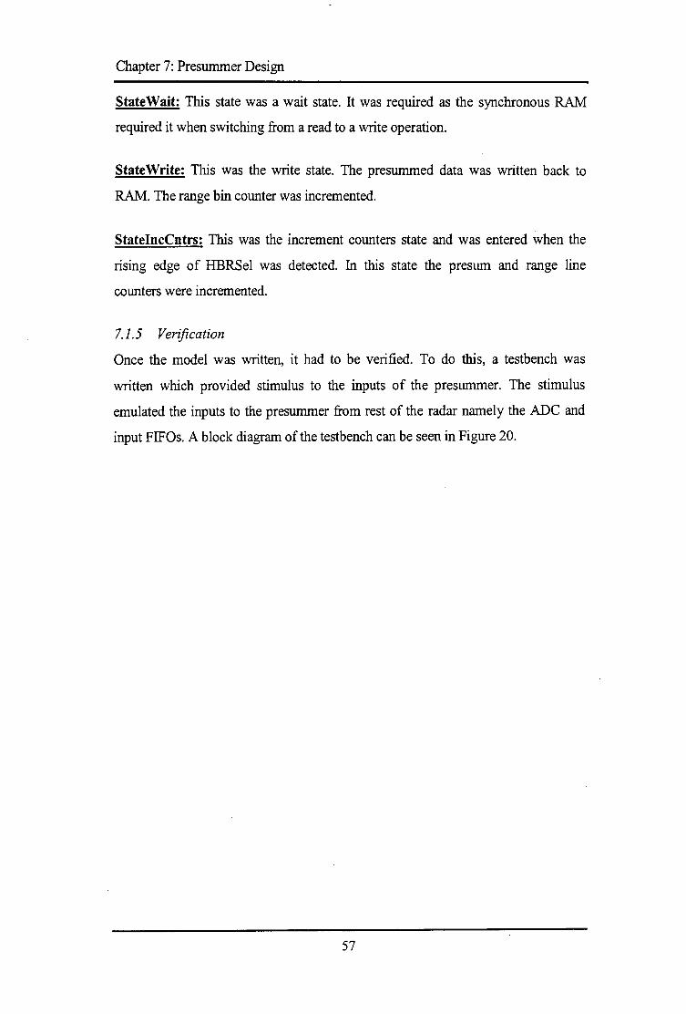
Chapter 7: Presummer Design
StateWait: This state was a wait state. It was required as the synchronous RAM
required it when switching from a read to a write operation.
StateWrite: This was the write state. The presummed data was written back to
RAM. The range bin counter was incremented.
StatelncCntrs: This was the increment counters state and was entered when the
rising edge of HBRSel was detected. In this state the presum and range line
counters were incremented.
7.1.5 Verification
Once the model was written, it had to be verified. To do this, a testbench was
written which provided stimulus to the inputs of the presummer. The stimulus
emulated the inputs to the presummer from rest of the radar namely the ADC and
input FIFOs. A block diagram of the testbench can be seen in Figure 20.
57
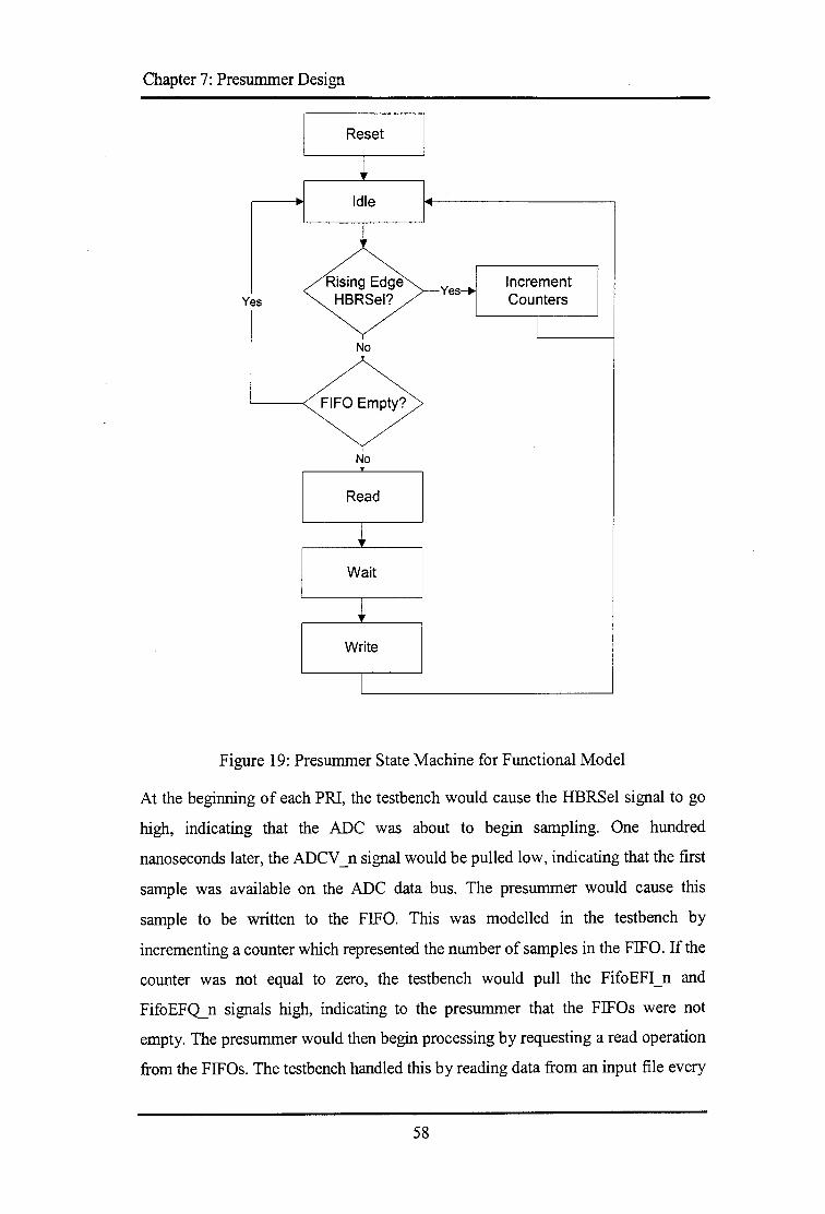
Chapter 7: Presumrner Design
Reset
Idle
Yes
No
FIFO Empty?
No
Read
Wait
Write
Yes Increment Counters
Figure 19: Presummer State Machine for Functional Model
At the beginning of each PRI, the testbench would cause the HBRSel signal to go
high, indicating that the ADC was about to begin sampling. One hundred
nanoseconds later, the ADCV _n signal would be pulled low, indicating that the first
sample was available on the ADC data bus. The presumrner would cause this
sample to be written to the FIFO. This was modelled in the testbench by
incrementing a counter which represented the number of samples in the FIFO. If the
counter was not equal to zero, the testbench would pull the FifoEFI_n and
FifoEFQ_ n signals high, indicating to the presumrner that the FIFOs were not
empty. The presumrner would then begin processing by requesting a read operation
from the FIFOs. The testbench handled this by reading data from an input file every
58
Chapter 7: Presummer Design
time a read operation was requested. At the same time, the counter which counted
the number of samples in the FIFO was decremented .
.........................
Presummer RAM
, ...................... ,
Output Data File
External Control Signal Generators
RAM Contol Signals (Address Counter, RnW
strobe etc
~--········································/·······················:
Objects within the dotted line represents
functions of the testbench
Figure 20: Presummer Testbench
The testbench was also responsible for writing presummed range lines to a disk for
later analysis. The presummer indicated to the prefilter that a complete range line
had been presummed by making the PSRowDone line active for one clock cycle.
The simplest way of accessing this presummed line was the same way that the
prefilter did so: using the second port of the dual port RAM. The testbench
contained a range line and range bin counter identical to those explained in 0. Every
time PSRowDone was made active, the testbench read a presummed range line
from RAM and wrote it to disk.
Using files for the input and output data simplified the verification process. The
same data that was used for the algorithmic simulation was sent through the
presummer. The results were then compared and the presummer was validated.
59
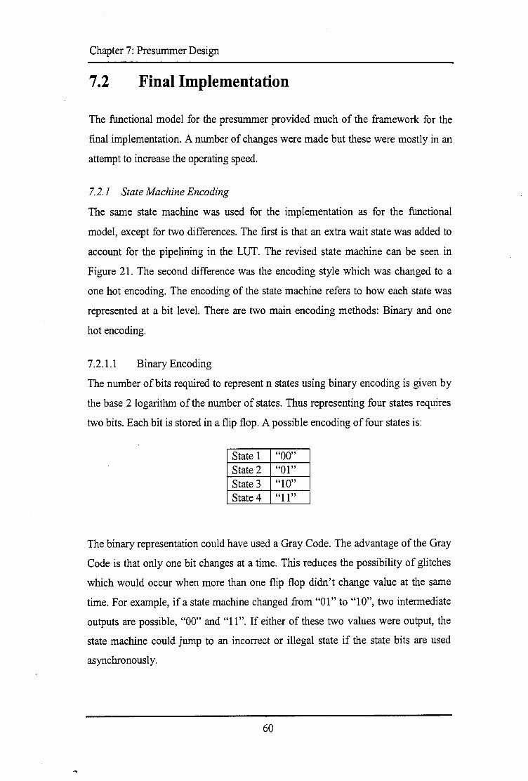
Chapter 7: Presummer Design
7 .2 Final Implementation
The functional model for the presummer provided much of the framework for the
final implementation. A number of changes were made but these were mostly in an
attempt to increase the operating speed.
7.2.1 State Machine Encoding
The same state machine was used for the implementation as for the functional
model, except for two differences. The first is that an extra wait state was added to
account for the pipelining in the LUT. The revised state machine can be seen in
Figure 21. The second difference was the encoding style which was changed to a
one hot encoding. The encoding of the state machine refers to how each state was
represented at a bit level. There are two main encoding methods: Binary and one
hot encoding.
7.2.1.1 Binary Encoding
The number of bits required to represent n states using binary encoding is given by
the base 2 logarithm of the number of states. Thus representing four states requires
two bits. Each bit is stored in a flip flop. A possible encoding of four states is:
State 1 "00" State 2 "01" State 3 "1 O" State 4 "11"
The binary representation could have used a Gray Code. The advantage of the Gray
Code is that only one bit changes at a time. This reduces the possibility of glitches
which would occur when more than one flip flop didn't change value at the same
time. For example, if a state machine changed from "01" to "10'', two intermediate
outputs are possible, "00" and "11 ". If either of these two values were output, the
state machine could jump to an incorrect or illegal state if the state bits are used
asynchronously.
60
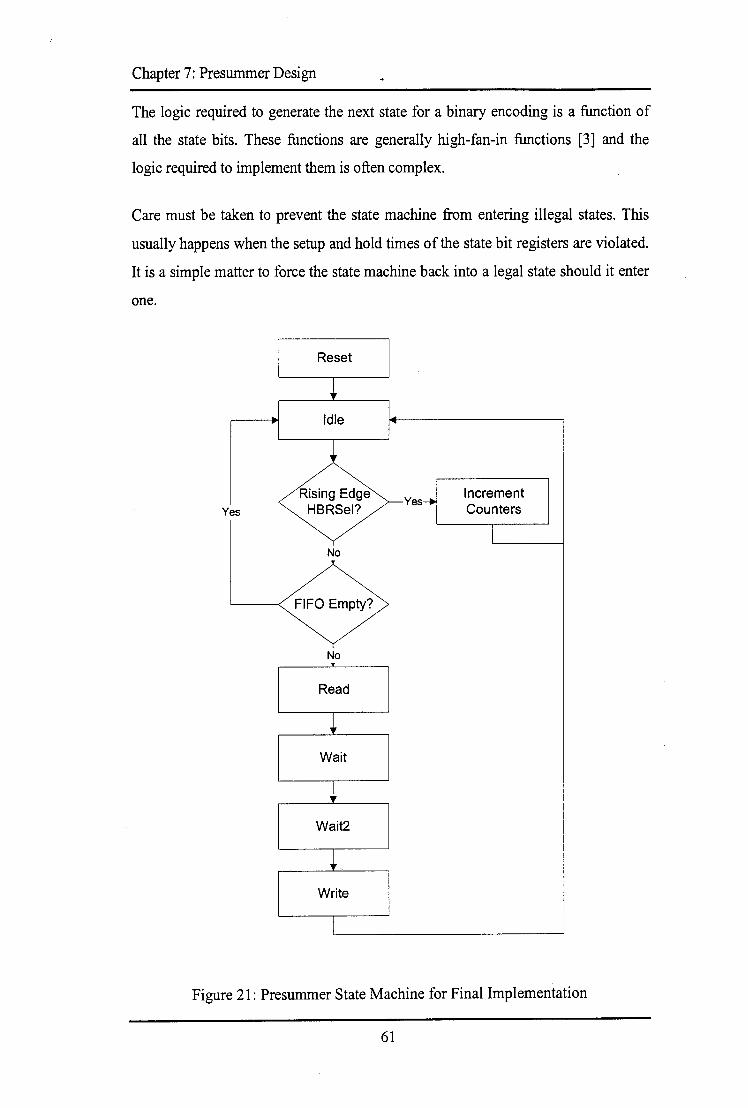
Chapter 7: Presummer Design
The logic required to generate the next state for a binary encoding is a function of
all the state bits. These functions are generally high-fan-in functions (3] and the
logic required to implement them is often complex.
Care must be taken to prevent the state machine from entering illegal states. This
usually happens when the setup and hold times of the state bit registers are violated.
It is a simple matter to force the state machine back into a legal state should it enter
one.
Reset
Idle
Yes
No
FIFO Empty?
No
Read
Wait
Wait2
Write
Yes Increment Counters
Figure 21: Presummer State Machine for Final Implementation
61
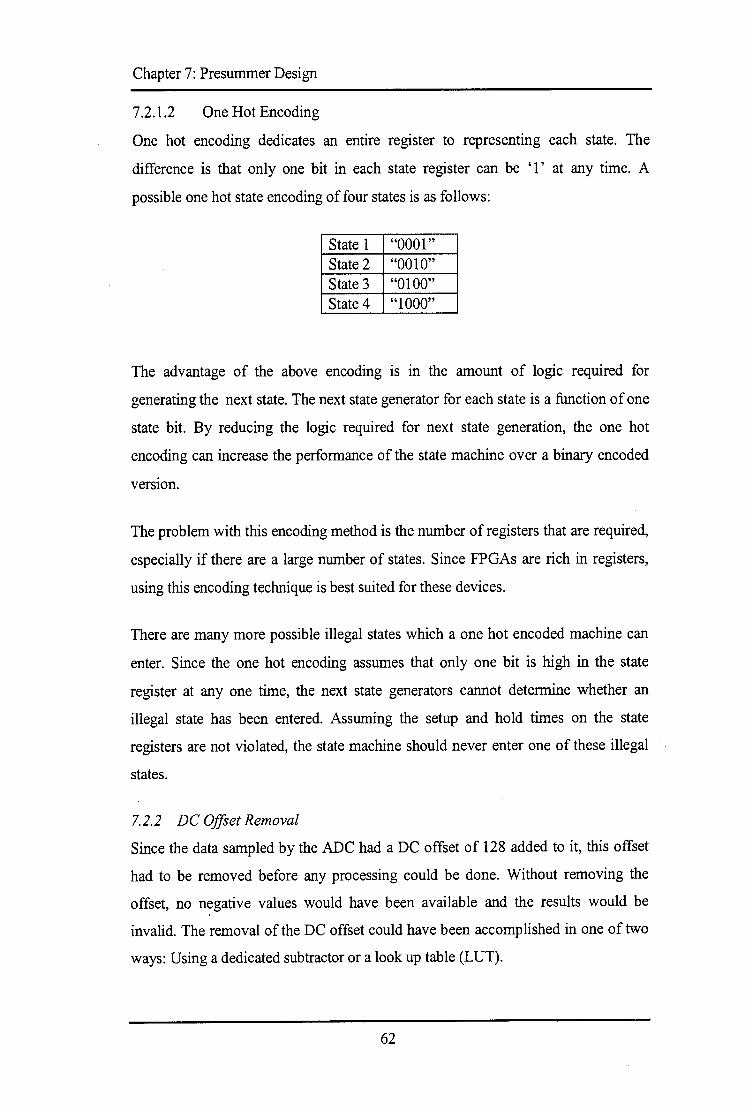
Chapter 7: Presummer Design
7.2.1.2 One Hot Encoding
One hot encoding dedicates an entire register to representing each state. The
difference is that only one bit in each state register can be 'l' at any time. A
possible one hot state encoding of four states is as follows:
State 1 "0001" State 2 "0010" State 3 "0100" State 4 "1000"
The advantage of the above encoding is in the amount of logic required for
generating the next state. The next state generator for each state is a function of one
state bit. By reducing the logic required for next state generation, the one hot
encoding can increase the performance of the state machine over a binary encoded
vers10n.
The problem with this encoding method is the number of registers that are required,
especially if there are a large number of states. Since FPGAs are rich in registers,
using this encoding technique is best suited for these devices.
There are many more possible illegal states which a one hot encoded machine can
enter. Since the one hot encoding assumes that only one bit is high in the state
register at any one time, the next state generators cannot determine whether an
illegal state has been entered. Assuming the setup and hold times on the state
registers are not violated, the state machine should never enter one of these illegal
states.
7.2.2 DC Offset Removal
Since the data sampled by the ADC had a DC offset of 128 added to it, this offset
had to be removed before any processing could be done. Without removing the
offset, no negative values would have been available and the results would be
invalid. The removal of the DC offset could have been accomplished in one of two
ways: Using a dedicated subtracter or a look up table (LUT).
62

Chapter 7: Presummer Design
Using a subtracter was considered but it was slower than the LUT equivalent. The
FPGAs used contained limited amounts of internal memory and it was decided that
since the resource was available, it should be used to speed up the design. The LUT
used was 256 x 8 bits as the data received from the FIFO was used as the LUT
address. The LUT was synchronous as the address was registered on each rising
clock edge and the data was latched out a clock cycle later.
7. 2.3 Pipelining
Pipelining is a method of increasing the throughput of a system by splitting it into
smaller modules. To illustrate, consider a four input adder shown in Figure 22.
Assume that each addition required time T to execute. The adder output would take
2T to calculate. Since this was a combinational circuit, the inputs A, B, C and D
have to remain constant for the duration of the addition. The throughput of this
adder is 1/(2T) and if it was used in a synchronous design, the maximum clock
speed would be 1/(2T).
Figure 22: Non Pipelined Four Input Adder
63
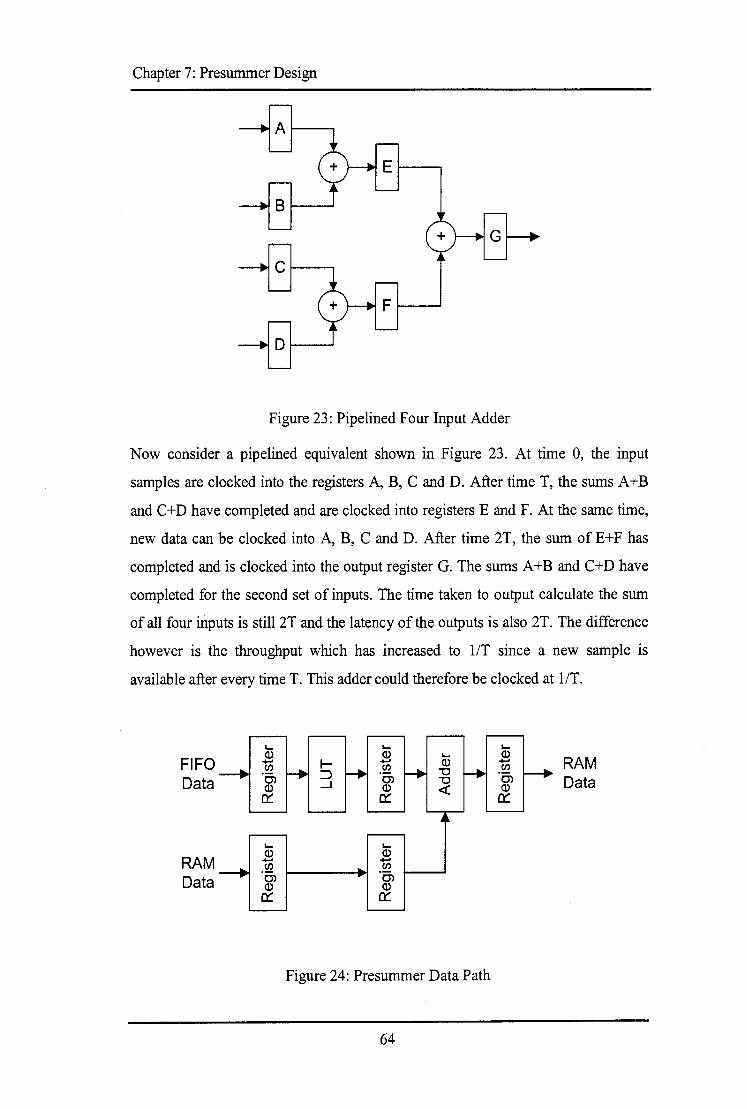
Chapter 7: Presummer Design
A--
DI-----'
Figure 23: Pipelined Four Input Adder
Now consider a pipelined equivalent shown in Figure 23. At time 0, the input
samples are clocked into the registers A, B, C and D. After time T, the sums A+B
and C+D have completed and are clocked into registers E and F. At the same time,
new data can be clocked into A, B, C and D. After time 2T, the sum of E+F has
completed and is clocked into the output register G. The sums A+B and C+D have
completed for the second set of inputs. The time taken to output calculate the sum
of all four inputs is still 2T and the latency of the outputs is also 2T. The difference
however is the throughput which has increased to 1/T since a new sample is
available after every time T. This adder could therefore be clocked at 1/T.
FIFO Data
RAM Data
'-CD
+-' (/) ·a, CD
0:::
Figure 24: Presummer Data Path
64
RAM Data

Chapter 7: Presummer Design
The presummer was pipelined to increase its throughput. During the initial design
stages, the length of the pipeline had to be decided upon. It was determined that the
RAM interface would be the bottleneck of the system since the same data bus had
to be used for reading and writing new data samples. The RAM required one clock
cycle in order to switch between read and write operations. If one sample was read,
processed and written back to RAM, the maximum utilisation of the RAM bus was
66% as one clock cycle in three would be wasted. Increasing the utilisation of the
RAM bus required that a number of samples be read and written for each clock
cycle lost. The function of the pipeline was therefore to maximise the use of this
interface by allowing a number of samples to be read before the RAM had to
perform write operations.
It turned out that the data arriving from the FIFO was sufficiently slow that the
presummer could process each new sample as it arrived. Since the time between
new samples arriving was much longer than the time it took to process one sample,
the pipeline was made as short as possible so that the latency was minimised. The
design however remained synchronous. A diagram of the pipelined data path can be
seen in Figure 24. The data from the FIFO and RAM arrived at the same time but
the FIFO data had a DC offset of 128 which was removed with a LUT. The LUT
required a clock cycle to complete so an extra register was required in the RAM
data path to synchronise it to the FIFO data. The adder used was pipelined and its
result was also registered.
7.2.4 Component Instantiation
As the name implies, a VHDL synthesiser can synthesise logic for a number of
given functions including multipliers and adders. Although the synthesis process
produces functionally correct logic, it is not always optimal for what the designer
intended. In the case of the presummer, two adders were required (I and Q
channels). The VHDL synthesiser was capable of producing these adders when the
addition operator was used in the source code, but faster adders could be obtained if
adder components were instantiated.
65
Chapter 7: Presummer Design
The instantiated components were provided by Altera and conformed to the Library
of Parameterised Modules (LPM) specification (see http://www.cdif.org/lpmweb).
LPM is an attempt by a number of EDA companies to produce a method of
technology independent design by creating a standard library of components. The
implementation of these components is left to the EDA tool vendors to create an
optimal instantiation for the targeted device. If the designer then moves to another
EDA tool vendor, the source does not need modification - the implementation is
merely changed by the new EDA tool.
Instantiating the adder components allowed more control over the adder's
performance. Most specifically, they provided a means of specifying the amount of
pipelining which was to be used in the adder. This increased the throughput of the
adder which was desirable. Another example of where component instantiation was
used was in the generation of the LUTs. The reason for doing this was again to
provide pipelining in the LUT.
The disadvantage of instantiating these components was that simulation models of
them were only unavailable for the Altera software. The VHDL simulator did not
support the LPM components and so the source code for the final implementation
could only be simulated in Altera's graphical simulation environment (see Section
2.3.3). Since this simulator did not offer a full set of VHDL functions e.g. file I/O,
the source code could not be simulated and checked by the testbench used in the
functional simulation (see Section 7.2.5 below).
When instantiating components in the VHDL source code, it is important that
simulation models of these components are provided. If the LPM components are
to be used, make sure that the simulator supports them too. The whole simulation
process cannot work if there are components which cannot be simulated.
7.2.5 Verification
Two aspects of the final implementation had to be verified: the functionality and the
timing. Ideally, the functional verification would take place by simulating the
synthesisable code and applying the testbench used in the functional simulation.
66
Chapter 7: Presummer Design
Once this was completed, the timing would be verified by using a model which
incorporated the timing delays found in the physical device.
The functional verification described above could not be performed because the
VHDL simulator used (Model Technologies' ModelTech ver 4.4j) did not have
provide simulation models for the components which were instantiated. Some of
functionality could be tested in Altera' s graphical simulator while the remainder
had to be performed when doing the timing verification. This was undesirable but
unavoidable as another VHDL simulator with LPM support could not be obtained.
After the FPGA software had performed a place-and-route of the logic which the
VHDL synthesiser had produced, it back annotated a VHDL model of the final
FPGA implementation. This VHDL model contained all the timing delays that
would be found in a physical FPGA. It was a gate level model where the
characteristics of the individual gates were modelled. A disadvantage of this type of
model was that all the signal names used in the synthesisable source are available
for debugging.
This model was then compiled and substituted for the functional model in the
presummer testbench. It was possible to do this as the back annotated model was
completely simulatable. The required test data was used as input to the simulation
and the results were compared with those obtained from the functional simulation.
The back annotated model was therefore responsible for the verification of the
device timing.
The execution time of the VHDL timing simulation was approximately 10 minutes
for each millisecond simulated. The simulation was performed on an Intel PII-
300MHz processor with 196MB RAM running Windows 95. The length of
simulation was determined by how much data was to be processed. Since 64 range
lines were to be stored in RAM, it was decided that at least that number had to be
passed through the model to ensure that all the counters were working correctly.
The result was that the simulation had to be run for a simulated time of 200ms
which took approximately 2 days.
67
Chapter 7: Presummer Design
The speed of this timing simulation did not lend itself to the typical method of
development where once a mistake was spotted, the entire design was recompiled
and then simulated until all the errors are found and corrected. This would have
been possible if the synthesisable source code was simulated as no place-and-route
operation was required and the simulation speed would have been faster as the
model would have been less detailed.
Debugging the simulation was equivalent to debugging a physical prototype except
that a number of simulator features made the task easier. The simulator allowed
traces to be plotted so that the values of individual signals could be monitored.
Breakpoints were supported in the simulator so that the execution could be stopped
at any point. The simulator could be run for a particular period of time or stepped
through or over individual lines of VHDL source. Watch windows allowed the
values of signals and variable to be monitored during this time. The only debugging
that could have taken place if a physical prototype were used was that the outputs
could be monitored with logic analyser. If any internal signals had to be checked,
the design would have to have been recompiled and place-and-routed with the
required signal routed to an output pin on the device.
7. 2. 6 Target Device
The presummer was implemented on an Altera EPFIOK10ATC144-1 device. This
was a 10000 gate FPGA in a 144pin Thin Quad Flat Package. The design occupied
approximately 30% of the device capacity. According to the design software the
maximum operating speed that device could operate at was approximately 50MHz.
68
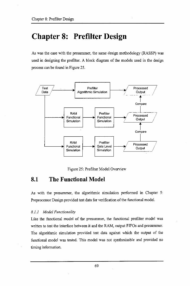
Chapter 8: Prefilter Design
Chapter 8: Prefilter Design
As was the case with the presummer, the same design methodology (RASSP) was
used in designing the prefilter. A block diagram of the models used in the design
process can be found in Figure 25.
Test Prefilter Processed Data Algorithmic Simulation Output
Compare
RAM Prefilter Processed
Functional Functional Output Simulation Simulation
Compare
RAM Prefilter Processed I Functional Gate Level Output Simulation Simulation
Figure 25: Prefilter Model Overview
8.1 The Functional Model
As with the presummer, the algorithmic simulation performed in Chapter 5:
Preprocessor Design provided test data for verification of the functional model.
8.1.1 Model Functionality
Like the functional model of the presummer, the functional prefilter model was
written to test the interface between it and the RAM, output FIFOs and presummer.
The algorithmic simulation provided test data against which the output of the
functional model was tested. This model was not synthesisable and provided no
timing information.
69

Chapter 8: Prefilter Design
8.1. 2 Prefilter Interface
Before a model could be written, the prefilter interface had to be decided upon. The
prefilter was required to interface with the presummer as it had to be signalled when
a new presummer line had been written to RAM. The prefilter also had to be able to
interface with the RAM as well as an output FIFO. A list of the input and output
pins of the prefilter can be seen in Table 5.
Table 5: Prefilter Interface Pins
Pin Description FifoDataI, FifoDataQ FIFO Output Data Bus (I & Q Channels). These
were each 8 bits wide Fifo~nl_n, FifoWEn2 FIFO Write Enable. Both need to be active to
allow a write on the next rising edge of the FIFO
Write Clock.
FifoRs n FIFO Asynchronous Reset RamAddr RAM Address Bus RamADS n RAM Address Strobe. When active, the value on
the RAM address bus is latched into the RAM on the rising edge of the RAM clock.
Ram CE RAM Chip Enable RamCntEn n RAM Address Counter Enable. When active, the
RAM' s internal address counter is incremented on each rising edge of the RAM clock.
RamCntRst n RAM Address Counter Reset RamDataI, RamDataQ RAM Data Bus (I & Q Channels) RamOE n RAM Output Enable RAMRnW RAM Read I Write Strobe RAMPipenFT RAM Pipeline I Flowthrough Strobe. This
toggles the RAM chip between Pipeline and Flowthrough modes.
Clk System Clock Reset n Asynchronous Master Reset PSRowinc Output from presummer. Active for 1 clock
period at the end of each presummed PRI.
8.1.3 Model Overview
A block diagram of the prefilter can be seen in Figure 26. The prefilter was
controlled by a state machine.
70

Chapter 8: Prefilter Design
Range Bin Counter
PRI Counter
Load Value
RAM Address
Start PRI Counter
RAM 1 FIR Filter H Divider H LUT ~FIFO Data Data
PS Row PS Row Counter State Machine FIR Counter
Done Decremen
Figure 26: Block Diagram of Prefilter
The prefilter had a presum counter which was used to record the number of
presummed lines in RAM at any time. This counter was incremented by one every
time the presummer output a PSRowDone signal on that line. After 32 presummed
range lines had been stored in RAM, the state machine would begin the processing.
The presummed data was read from RAM and input into the FIR filter. After 32
samples had been processed by the filter, the output was latched so that the FIR
filter could continue processing a new set of data while the final output was being
calculated.
The final output had to be in the form of an eight bit, unsigned integer with a DC
offset of 128. In order to achieve this, the FIR filter output had to be divided by the
sum of the magnitude of filter coefficients multiplied by the presum factor. This
resulted in an output in the range -128 to 127. This value was then added to 128 to
produce an unsigned integer in the range 0 to 255. This value was then written to
the output FIFO.
Since only 64 range lines were stored, the data had to be wrapped around in
memory. This was especially necessary since the presummer had to continue
writing data to RAM while the prefilter was reading the 32 range lines required for
71
- .......... _.,,="'·"'-'-" ·=···=" """--'="·-=.--=·"·=""="·:::.:.:·, .. =·-::_•· :.;::""=··=·~=··n"'-'""=·-·===· .. ··=-"""-'' ·=·· •_,;;,·•_;;,;··•""-· =· .. ·,;:;;·•".:..,;·· ',::.''''"'"''.-::.:.."•"""'"""""'"~
Chapter 8: Pre:filter Design
its processing. For this reason, three counters were used for the RAM address. The
first was a range bin counter (12 bits) while the second was a range line counter (6
bits). These were concatenated to provide the RAM address as in the presummer
(see Figure 17 and Figure 16). A start sample counter (6 bits) was the third counter
used and provided the reload value for the range line counter.
When the data from each new range bin was to be read into the FIR filter, the range
line counter was preloaded with the value of the start counter. The range line
counter was then incremented 32 times to read the required values from RAM. This
counter would roll over at a count value of 63 so that the data could be wrapped
around in memory. After 32 data values had been read, the range bin counter was
incremented and the process repeated. In this way, all the required data could be
read while the presummer continued to write new data to RAM. Note that since the
pre:filter had to produce a pre:filtered range line every 12 PRis, there would never be
a situation where the presummer would overwrite data which had not been :filtered.
Once a complete range line had been :filtered, the presum counter was decremented
by 4, since 4 was the skip factor. The remaining 28 range lines stored in RAM were
required for the next range line filter.
8.1.4 State Machine
A state machine was used to control the pre:filter and all its external outputs. The
operation is described below and can be seen in Figure 27.
StateReset: This was the reset state. All the RAM address counters were reset.
Stateldle: This was the idle state. The state machine remained in this state until the
presummer had written 32 range lines to RAM. When this occurred, the state
machine would advance to the read state. The RAM address counters were reset in
the idle state.
StateRead: This was the read state. The state machine remained in this state until
32 samples had been read from RAM into the FIR filter. This state used a down
counter to count the number of clock cycles which occurred while in this state.
72

Chapter 8: Pre.filter Design
When the down counter reached zero, the state machine moved to the next state. A
down counter was used as it was the most efficient method of waiting for a set
period of time. The alternative was to create the same number of wait states as clock
cycles to be waited. That would have been very inefficient and was not
implemented.
StatelncCntrs: This was the increment counters state. It was entered at the end of a
read and was used to increment the address counters and reload the range line
counter.
StateDecPSRows: This was the decrement presummed rows state. It was entered at
the end of processing a range line and was used to decrement the presum counter.
8.1.5 Verification
A testbench was written to read the data output by the presummer testbench and
pass it through the prefilter. The data output by the prefilter was then written to disk
to be compared with the algorithmic simulation results. A block diagram of the
testbench can be seen in Figure 28.
On startup, the testbench would write the 64 ranges lines of data to the one port of
the RAM, asserting the PSRowDone signal for one clock cycle at the end of each
PRI written. When the prefilter detected that the required number of rows (32) had
been written, it would read the data from the other RAM port, process it and output
the result. The prefilter would assert the output FIFOs write enable signal when the
processed sample was ready for output. The testbench used this signal to write the
processed value to disk. These results were then compared with those obtained from
the algorithmic simulation to verify the operation of the functional model.
The test data was prefiltered and the correct data was output.
73
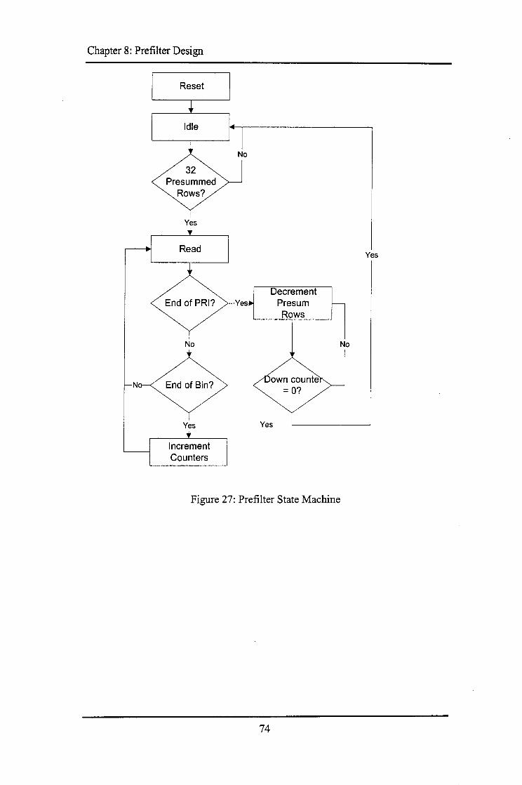
Chapter 8: Prefilter Design
Reset
Idle
Presummed Rows?
Yes
Read
End of PRI?
No
N End of Bin?
Yes
Increment Counters
No
Yes Decrement
Presum Rows
Yes
Figure 27: Prefilter State Machine
74
Yes
No
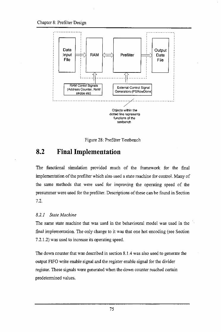
Chapter 8: Prefilter Design
......................... , , .......................... ,
Data Input File
RAM
RAM Contol Signals (Address Counter, RnW
strobe etc
Prefilter
External Control Signal Generators (PSRowDone
Output Data File
'. .......................................... /·······················;
Objects within the dotted line represents
functions of the testbench
Figure 28: Prefilter Testbench
8.2 Final Implementation
The functional simulation provided much of the framework for the final
implementation of the prefilter which also used a state machine for control. Many of
the same methods that were used for improving the operating speed of the
presummer were used for the prefilter. Descriptions of these can be found in Section
7.2.
8.2.1 State Machine
The same state machine that was used in the behavioural model was used in the
final implementation. The only change to it was that one hot encoding (see Section
7.2.1.2) was used to increase its operating speed.
The down counter that was described in section 8.1.4 was also used to generate the
output FIFO write enable signal and the register enable signal for the divider
register. These signals were generated when the down counter reached certain
predetermined values.
75
Chapter 8: Prefilter Design
8.2.2 FIR Filter
A few options existed for implementing the FIR filter. The first was to use a FIR
filter module written by Altera. This module claimed operation speeds of up to
1 OOMHz, variable input data widths, output data widths and internal precision. The
filter also had an option to include pipelining. The problem with this filter was that
is was only available in 8, 16, 32 and 64 taps and the coefficients had to be either
symmetric or anti-symmetric. The second option was to use the FIR filter module
provided by Synopsys. After further investigation it turned out that a licence for this
module was unavailable and so it could not be used. The last option was to write a
FIR filter but this implementation would not have been an optimal solution. The
module from Altera was chosen as the implementation that would be used. The
filter coefficients had to be recalculated to for a filter length of 32.
The filter core was only available in AHDL, a proprietary hardware description
language by Altera. This posed a problem in compiling and simulating the prefilter
as Altera's MaxPlus2 software was the only software that could read AHDL. Since
using this module provided the only real option for implementing a FIR filter, it had
to be used.
Unlike the Synopsys FIR filter which could load new coefficients during its
operation, the Altera FIR Filter's coefficients were specified at compile time. If the
system was required to change filters during operation, it was possible to load the
FPGA with a new precompiled configuration with different coefficients.
To optimise the FIR filter, Altera made use of LUT-based vector multipliers [2].
The coefficients were divided into partial products which were then added together.
Performing addition operations were faster than multiplications. This resulted in a
very fast FIR filter. The required coefficients were input to an Altera supplied
program which calculated the partial products. The partial products were then
linked into the design when the FIR filter module was instantiated.
Since the FIR filter was written in AHDL and the rest of the presummer was written
in VHDL, a method of combining these had to be found. The solution was to use
the graphical schematic entry tool in MaxPlus2. The required FIR filter components
76

Chapter 8: Prefilter Design
were instantiated and after the VHDL section was compiled, a schematic symbol
was created for it. This was then connected to the FIR filter in the schematic editor.
In this way, the two major components of the prefilter were combined into one
entity.
Although the documentation [1] claims that the bit widths of the filter coefficients
can be independently specified of the data bus width, this appears to be inaccurate.
The initial design made use of ten bit data and eight bit coefficients. The FIR filter
operated correctly when an impulse function was passed through it - the values of
the coefficients were output. Any other input data produced an incorrect output on
at least one of the filter tap outputs. It was thought that the problem was due to the
internal precision (precision of the calculations) of the filter but this was excluded
for two reasons: Firstly, when the internal precision was increased, the problem
remained. Secondly, the values used for testing were too small for overflow to
occur. No pattern seemed to exist which would predict which coefficient would
cause the incorrect value to be output. The problem was finally solved by increasing
the precision of the filter coefficients to ten bits. Although their values remained
unchanged, the problem was solved. The cause of the problem is still not know.
8.2.3 Dividers
The output of the FIR filter was 23 bits wide to prevent loss of dynamic range or
overflow. This output contained a gain associated with the filter coefficients as well
as a gain introduced by the presumming. The presum gain was three, the number of
lines that were presummed. The filter gain was equal to the sum of the absolute
value of the coefficients. This equalled the maximum gain that the FIR filter could
apply to any data stream. The filter gain for the coefficients used was 952 (see
Appendix A: FIR Filter Characteristics for details on the coefficients). The FIR
filter output therefore had to be divided by 2856 to scale the result down to eight
bits.
Altera provided a divider core that was initially used. This core was configurable as
the bit widths of the inputs and outputs could be modified, as well as the number of
77

l ..
Chapter 8: Prefilter Design
pipeline stages. During final testing it was discovered that the divider could only
operate on unsigned values. Another solution had to be found.
A number of alternatives were examined. The first was to perform a partial
fractional decomposition of the division by 2856 into a number of powers of 2. The
values of a, b, c, d and e in Equation 5 were computed using a PBIL based search
program written by Richard Lord which made use of the algorithm described in [ 6].
The number of partial fractions to use was variable but four seemed to give a good
trade off between accuracy and the amount of logic required to implement. The
final approximation used can be seen in Equation 6. By making use of divisors
which were powers of two, the division could be performed with an arithmetic right
shift operation.
Equation 5
These partial fractions could then be added which was faster than a division
operation. The error in the approximation was approximately 3x10⁻⁶. The problem
with the implementation of this was that truncation errors were introduced in the
division. Since the representation of the data was in the form of integers, no
fractional parts of the results were stored or used. This truncation error was
compounded since it occurred in the calculation of each partial fraction. This
resulted in incorrect values and an alternative solution was investigated.
1 1 1 1 1 --~-+-+-+-2856 212 214 215 217
Equation 6
The solution implemented made use of the unsigned divider provided by Altera.
The data output from the FIR filter was examined to determine if it was positive or
negative. The absolute value of the output was taken and this unsigned value was
input to the divider. The output of the divider was then sent to two LUTs, one for
positive values and one for negative values. The function of the LUT was to convert
the divider output into the eight bit, unsigned value required for output. Two LUTs
were required since different offsets were required for positive and negative values.
78
Chapter 8: Prefilter Design
A multiplexer was used to connect the two LUTs outputs to the FIFO data port. The
select signal for the multiplexer was controlled by the most significant bit of the
FIR filter output. If it was a logic '1 ', the number was negative. This method
worked correctly.
8.2.4 DC Offset
Since the original data had a DC offset of 128, this offset had to be reinstated before
the data could be output. To do this, a LUT was used, as in the case of the
presummer.
As described in Section 8.2.3, the divider could only operate on unsigned values.
The absolute value of the numerator was used in the dividing process. Instead of
providing an output in the range -128 to 127, the output range was 0 to 128. Since a
DC offset had to be added to these values, it was decided to make use of two LUTs,
one for negative numerators and the other for positive numerators. The LUTs were
different as different offsets had to be added depending on the sign of the
numerator.
The LUT for positive numerators was 127x8 bits. This LUT merely added the
required 128 to the quotient to map the positive output values to the range of 128 to
255.
The LUT for negative numerators was a little more complex. The range of quotients
was 0 to 128. The reason for this was that two's complement representation of
integers has a larger range for negative number than positive ones. A LUT of 256x8
bits was required to hold the offset output values. There was no constant DC offset
that was added to these values - the offset had to be equal to the negative of the
input value added to the required DC offset of 128. The output range of 0 to 128
was therefore mapped to the range 128 to 0.
A multiplexer was used to select the required .output from the positive and negative
LUTs. The selection signal for the multiplexer was taken from the MSB of the FIR
filter output. The MSB was the sign bit of the value. When it was '1 ', the number
was negative.
79
__ · __ . _____ ·-_"".'·:_:_':_~: _ _::_:_·_:_.:__:__:·· ..
i
l~_'" ___ ,. ___ ~-----------
Chapter 8: Prefilter Design
8.2.5 Verification
The final implementation was verified in two steps. Its functionality was first tested
in the Altera MaxPlus2 Environment. The timing was then tested using a back
annotated VHDL model of the prefilter. This model was used in conjunction with
the functional model testbench described in Section 8 .1.5.
The prefilter design was large and the entire compilation process took a number of
hours to compile and fit. The Altera software provided an option to compile the
design for a functional simulation. This simulation was performed on the
synthesised logic and no place-and-routing took place. This reduced the compilation
time to under an hour which made the debugging process more feasible. The
problem with this was that only the Altera graphical simulator could be used as no
other simulator supported AHDL components. The Altera simulator did not support
the use of testbenches. If VHDL simulation models had existed for all the
components used, this method of verification would have been unnecessary as the
VHDL source could have been simulated before being place-and-routed. Due to the
size of the design, this simulation was time consuming. It took approximately 1 min
to simulate 1 us.
Once the functionality of the prefilter implementation had been verified, its timing
had to be tested. The MaxPlus2 design software provided this information in a back
annotated gate level VHDL model. This model was very large (approximately
18MB of VHDL source!). Simulation times were very slow due to the size and
complexity of the model which included setup and hold time checks on the input
signals. This simulation was performed on an Intel PII-300MHz with 196MB RAM
and took approximately 24 hours to simulate 5ms of time. This was unacceptable as
it would have taken approximately 60 days of simulation time to thoroughly test the
timing of the entire design. The only aspect that was not tested in the timing model
was the address counter overflows but these were verified in the functional
verification.
The same input that was used in the functional model was to verify the final
implementation timing model. The processed outputs were compared and were
80

I
Chapter 8: Prefilter Design
identical. The timing of the inputs to the FPGA were tested by the back annotated
model, while the outputs to the RAM and FIFO were inspected visually. Traces of
the signals were plotted and the setup and hold times were measured and verified.
8.2.6 Target Device
The prefilter was fitted to an Altera EPFl OKI OOARC240-1 device. This was the
fastest 100000 gate device that Altera made at design time. The device was
approximately 81 % full. A larger capacity device should have been used if the
design was likely to undergo modification, especially if pin locking was needed.
Since this was not the case, however, the 100000 gate device was used.
According to the design software, the maximum registered clock speed that could
be used was 44MHz. The slowest part of the design was the divider whose
propagation delay was approximately 23ns.
The operating speed was more than adequate for the prefilter to operate correctly. If
the design was to be produced on a large scale, the use of a slower device could
have been investigated. Combining the presummer and prefilter onto one FPGA
could also have been investigated as a means of reducing costs.
81
1 ........ ·, "' ····;• .. •·.·;:.,··""'';•oo· .. ·c"''-""""•' ".:•-"'' :" , • ------ - - - ··- --;.~~··:. :~:~: ... _~·~ ,
Chapter 9: Conclusions and Recommendations
Chapter 9: Conclusions and
Recommendations
The following conclusions were drawn from the work performed as described
above.
It is impossible to validate the goals of RAS SP from this case study. A comparison
would have to be performed with the design of the same system using non-RASSP
design techniques. What can be concluded is that Virtual Prototyping is a useful
tool when designing digital circuits although it need not be used in every design.
The overhead required in writing the models required needs to be weighed against
the decrease in debugging time. This is particularly true of small designs.
The first important criterion for a successful system level simulation is that all the
entities and components used must have VHDL simulation models. One of the
larger problems encountered was that the VHDL source files could not be simulated
by the VHDL simulator because certain components which were instantiated had no
VHDL simulation models. If the source files could be simulated in the simulator,
the debugging time would have been reduced as a VHDL simulator is more
powerful and contains more features than the graphical simulators which
accompany many of the FPGA design packages. For systems which employ more
complex devices like DSPs and micro-controllers simulation models would have to
be purchased as they have a long development time and omitting them from the
simulation would defeat the purpose of the simulation.
Virtual prototyping has advantages in that the cost of debugging is small (excluding
the billable time for those who are performing the debugging). Once an error is
found, it can be corrected in software and the system simulated again. If the error
was found in the physical prototype, it could possibly be corrected in software
although often a hardware modification would be required.
82
Chapter 9: Conclusions and Recommendations
Gate level simulations are impractical for large designs. The time required to
simulate the design can be longer than the time required to build a physical
prototype, as was the case in this case study. The functionality of the final
simulation can be verified without using a gate level simulation if all the
components used have simulation models, or their VHDL source code is available.
The use of FPGAs in DSP systems is definitely practical and excellent results can
be obtained. The decision on whether to use an FPGA or dedicated DSP must be
taken in light of the tasks to be performed although the following guidelines can be
applied: Floating point operations are not suited to FPGAs as most of the available
components only support integer operations. Multiplication and division operations
are costly in terms of resource usage.
Although a seemingly obvious point, the architecture of a DSP is fixed, compared
to the FPGA whose architecture is specified by the designer. A greater amount of
flexibility is offered by the DSP when modifications are required. To modify the
operation of an FPGA often requires the designer to make major architectural
changes, unlike the DSP programmer who changes a few lines of source code.
Having said this, the use ofVHDL has progressed the design ofFPGAs a long way
down the road to supporting quick design modifications. If the synthesisable
description of the FPGA is written at a high level, making changes in its operation
is not much more complex than adding a few lines of VHDL code. For DSP type
work, the designer is likely to specify the architecture of the FPGA at a low level so
that the operating speed can be maximised. This is because since the lower the
abstraction level of the synthesisable code, the more control the designer has over
the synthesised result.
The majority of VHDL simulators on the market are event based simulators. Cycle
based simulators are making their appearance with claims of 1 Ox speed
improvements over event driven simulators for gate level simulations. It would be
interesting to test these claims as increasing simulator speeds could make gate level
simulations of large systems feasible. Testing other simulators which ran on
multiprocessor computers would further test the feasibility of gate level simulations.
83

Appendix A: FIR Filter Characteristics
Appendix A: FIR Filter
Characteristics
This appendix details the characteristics of the different FIR filters tested and the
results of their testing. The first three filters were created using the algorithm
described in [16]. The first of the three filters was designed to operate with no
presummer i.e. the sampling frequency was 625Hz and had 64 taps. A 32 tap
equivalent could not be constructed since there were too few taps to specify a cutoff
frequency of 20Hz. The second and third filters were used to compare the effects of
64 and 32 tap filters with a sampling frequency of 208.33Hz.
The remaining filters were constructed to determine the best 32 tap filter which
would operate with a sampling frequency of208.33Hz.
The coefficient values used for the testing can be found in Table 6 on page 91.
84

Appendix A: FIR Filter Characteristics
A.1 Filter A
The frequency response of this filter can be seen in Figure 29. The filter was
designed to operate on data which had been sampled at 625Hz and has 64 taps. The
an optimal method was used for designing the coefficients and can be found in [ 16]
20
ili' ~ ill c: 0
~ 0 "' ~ j ii:
50 JOO J50 200
Frequency [Hz]
Figure 29: Frequency Response of Filter A
A graph of the filter tap coefficients can be seen Figure 30.
JOO
50
0 JO 20 30 40
Tap Number
0
Q GI
0 'q
<ll !!>
\
50
GI GI
Figure 30: Coefficients of Filter A
85
250 300
Gl°oa eGI
60

Appendix A: FIR Filter Characteristics
A.2 Filter B
This filter was created using the same method as Filter A above. It also contained
64 taps but was designed to operate on data which was sampled at 208.33Hz. Its
frequency response can be seen in Figure 31 and its coefficients can be seen in
Figure 32
Iii' 0 ~ ~ r:: 0 Q.
"' "' p: ... ~ ~ -20
100
~ r:: 0
~ "' p:
~
= 50 Q.
.§ ... ~ ~
0
20 40 60
Frequency [Hz]
Figure 31: Frequency Response of Filter B
10 20
I
9
0 I
I
I I
I I
9 9
30
I
I
Q;)
0 I
Tap Number
40
Figure 32: Coefficients of Filter B
86
50
80 100
60
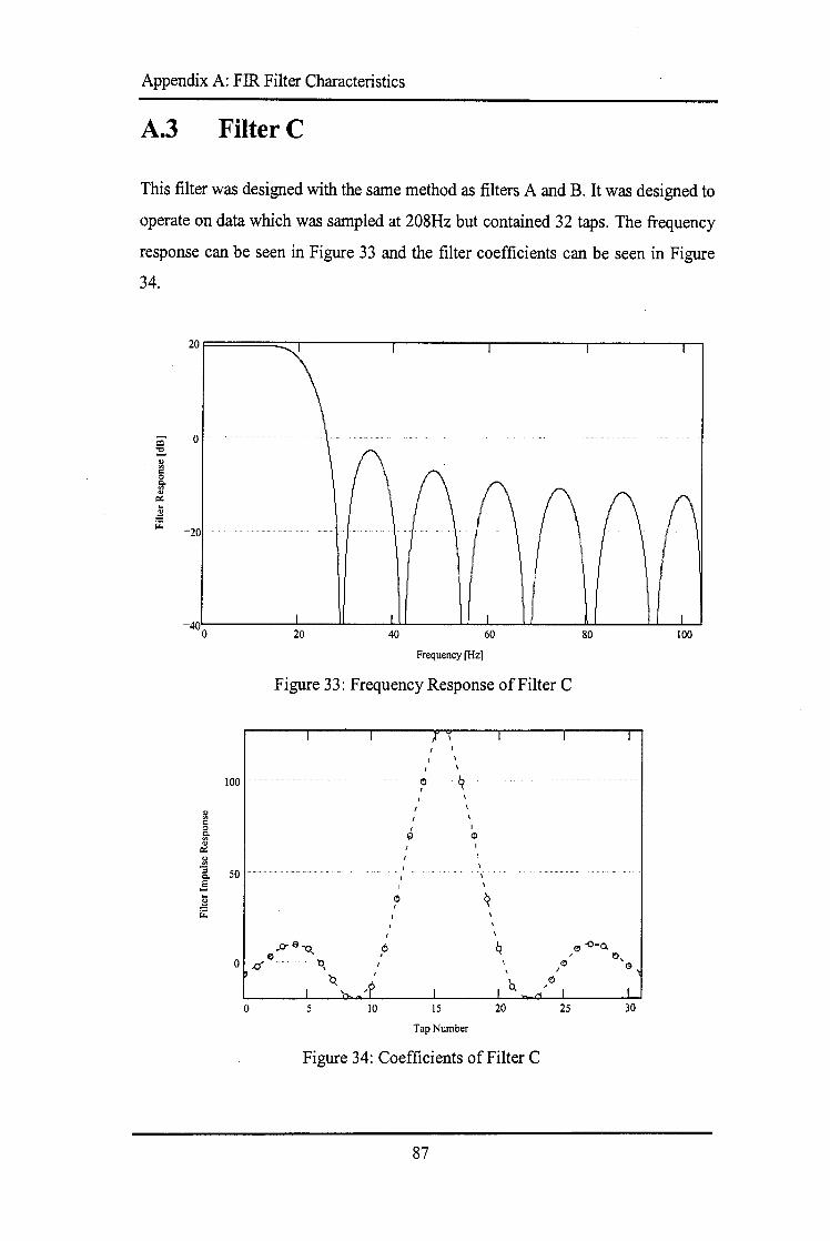
Appendix A: FIR Filter Characteristics
A.3 Filter C
This filter was designed with the same method as filters A and B. It was designed to
operate on data which was sampled at 208Hz but contained 32 taps. The frequency
response can be seen in Figure 33 and the filter coefficients can be seen in Figure
34.
;Ii' 0 ~ ~ c 0 Q,
"' " ~ ... 1! ~
-20
100
50
0
20 40 60
Frequency [Hz]
Figure 33: Frequency Response of Filter C
I
~
0 I
,6
5 JO
I
I
0 I
15
Tap Number
I
CD
\ ,.
20
Figure 34: Coefficients of Filter C
87
25
80 JOO
30

Appendix A: FIR Filter Characteristics
A.4 Filter D
This filter was designed using a Kaiser Window. It was a 32 tap filter designed to
operate on data sampled at 208Hz. Its frequency response can be seen in Figure 35
and its filter coefficients in Figure 36
Iii" ::=.. 1,l c:: 0
~ " ~ -~ ~
0
-zo
-40•~~~~~~~~~~~~~~~~~~~~~~~~~~~~
0 20 40 60 80 100
100
0
Frequency [Hz]
Figure 35: Frequency Response of Filter D
I Q. ,
5 10
I
I
I
I
0
I
I
I
<l>
0 b I I
I I
<!> I
15
Tap Number
I!) I
I ., I G)
I G)
20
I (I)
, -0
Figure 36: Coefficients of Filter D
88
,o
25 30
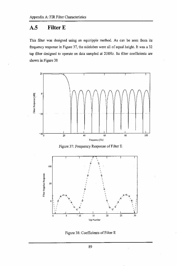
Appendix A: FIR Filter Characteristics
A.5 Filter E
This filter was designed using an equiripple method. As can be seen from its
frequency response in Figure 37, the sidelobes were all of equal height. It was a 32
tap filter designed to operate on data sampled at 208Hz. Its filter coefficients are
shown in Figure 38
Iii:' 0 ::.. 1;l c 0
fil" "' ..: -~ ii: -20
-400 20 40 60 80 100
Frequency [Hz]
Figure 37: Frequency Response of Filter E
I I ,r -, I I I /
I q ~
100 I
I I
I
1;l 9 0 c 0 I
fil" I
"' I ..: 1;l 50 :; Q. \
.§ Cl) Q - I
~ ..0-0 ,,..e -O,Q ii: b e '
Gl p Cl)
Q I ~ 0 ·~
I ~ I ,<!! I
I I \ I \
I I 'a. I I /
I e> Q <> I I I' o' yj ,, 1'
" I I I I I .,
0 5 • JO 15 20 25 30
Tap Number
Figure 38: Coefficients of Filter E
89
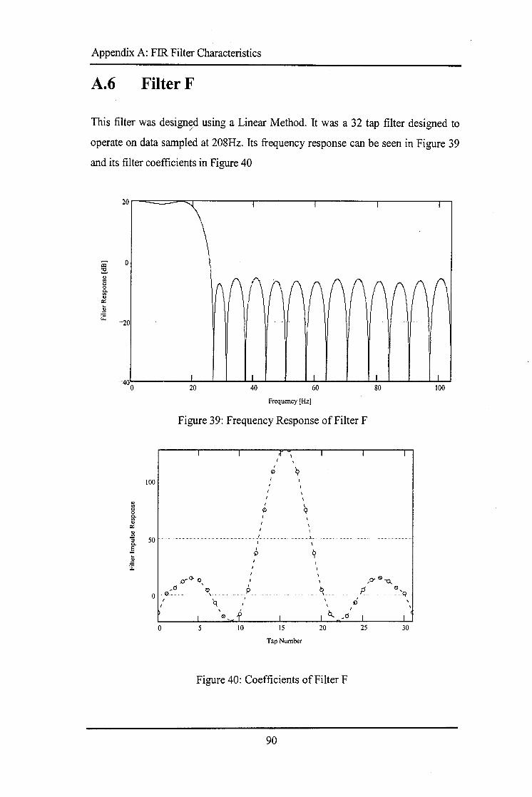
Appendix A: FIR Filter Characteristics
A.6 Filter F
This filter was designed using a Linear Method. It was a 32 tap filter designed to /
operate on data sampled at 208Hz. Its frequency response can be seen in Figure 39
and its filter coefficients in Figure 40
Iii' 0 ~ ~ c 0
~ OJ ~
j ~ -zo
100
20 40 60
Frequency [Hz]
Figure 39: Frequency Response of Filter F
()~C> 0
I
I
I 9
I
0
I
I
I
Q
~d '~ 0 ~.... \
,' 'q
0 IO 15 20 25
Tap Number
Figure 40: Coefficients of Filter F
90
80 100
30

Appendix A: FIR Filter Characteristics
A. 7 Table of Filter Coefficients
The filter coefficients found in Table 6 were scaled to eight bit, signed integers.
These coefficients were used in the testing of the FIR filters described above.
Table 6: FIR Filter Coefficients
Tap Number Filter A Filter B Filter C Filter D Filter E Filter F 1 -3 0 -6 -7 14 -16 2 0 2 -2 -3 -38 1 3 1 2 2 3 -1 6 4 4 0 8 10 12 12 5 6 -1 9 14 16 15 6 8 -3 7 12 15 13 7 10 -3 0 3 6 4 8 12 -2 -10 -9 -5 -7 9 15 0 -19 -21 -19 -19
10 19 3 -20 -25 -26 -24 11 23 5 -13 -18 -20 -17 12 27 4 6 4 0 4 13 32 1 34 37 33 37 14 37 -2 70 75 72 75 15 43 -6 99 108 107 108 16 48 -8 127 127 127 127 17 54 -6 127 127 127 127 18 60 -1 99 108 107 108 19 66 5 70 75 72 75 20 72 11 34 37 33 37 21 78 13 6 4 0 4 22 84 9 -13 -18 -20 -17 23 90 0 -20 -25 -26 -24 24 95 -12 -19 -21 -19 -19 25 100 -22 -10 -9 -5 -7 26 104 -24 0 3 6 4 27 108 -15 7 12 15 13 28 112 6 9 14 16 15 29 114 38 8 10 12 12 30 118 74 2 3 -1 6 31 119 106 -2 -3 -38 1 32 127 127 -6 -7 14 -16 33 127 127 34 119 106 35 118 74 36 114 38
91

-----------------------------------------.......
Appendix A: FIR Filter Characteristics
Tap Number Filter A Filter B Filter C Filter D Filter E Filter F 37 112 6 38 108 -15 39 104 -24 40 100 -22
-- 41 95 -12 42 90 0 43 84 9 44 78 13 45 72 11 46 66 5 47 60 -1 48 54 -6 49 48 -8 50 43 -6
.. · 51 37 -2 52 32 1 53 27 4 54 23 5 55 19 3 56 15 0 57 12 -2 58 10 -3 59 8 -3 60 6 -1 61 4 0 62 1 2 63 0 2 64 -3 0
92

Appendix B: JTAG Boundary Scan
Appendix B: JTAG Boundary Scan
With the package pin density of many I Cs increasing rapidly, conventional methods
of testing assembled PCBs are failing to perform adequately. The most common
device used for testing assembled PCBs today is the "bed of nails" tester. This
device has a number of nail-like probes which are placed on the ICs on the PCB.
Different probes are driven by the tester and other probes are then read to see if the
correct connection between these test points had been made. The fundamental
assumption when using such a tester is that all the pins of the ICs are accessible.
This is most certainly not the case with many of the new IC packages e.g. the Ball
Grid Array. This is a surface mount device where the "pins" are under the device -
inaccessible to any probes.
This problem was recognised and in 1985 and the Joint Test Action Group (JTAG)
was formed in an attempt to overcome this problem. Their solution was made an
IEEE standard (IEEE 1149 .1-1990) and is in use today although it is often still
referred to as JTAG. The JTAG solution was to build the test circuitry into the
devices, rather than requiring external hardware.
JTAG compliant devices have a 4 pin JTAG port which allows access to the
boundary scan hardware. Instructions are loaded into the device in a serial manner
while the results are serially read form the device. A number of devices can be
connected to the JTAG port in a serial manner. The 4 pin port required on every
JTAG port contains two control signals, an input and an output port.
The IEEE Standard IEEE 1149 .1-1990 requires that a certain set of instructions be
implemented in the boundary scan hardware although the designer is able to able to
add support for additional commands [18]. Many of the FPGA manufacturers have
extended this port to allow for programming of the devices.
93
Appendix C: MathCAD SAR Processor
Appendix C: MathCAD SAR
Processor
Below is a listing of the MathCAD SAR processor used to test the effects of a
presummer and prefilter on SAR processing. The processor generated the returns
from a point target which it then presummed and FIR filtered. The presum factor
was user definable as was the length of the FIR filter. The coefficients for the filter
were read from an ASCII text file. The processed returns were used to construct a
matched filter which was then convolved with the processed data. The power values
for the focussed image were written to disk where they were analysed by a peak
detection program written by Jasper Horrell. The peak width, measured in number
of samples, was then input to the processor and the focussed azimuth resolution was
then calculated. This was one of the values used to measure the performance of the
presummer and FIR filter.
Simple SAR Processor with presummer and filter support fc =14l·MHz
Radar carrier frequency f PRF = 625- Hz
Radar PRF
c =3·108·~ sec
A=~ fc
A=2.12am
v ·=250~ sec
Speed of aircraft 0 BW =45·deg
Antenna beamwidth Rt =6·km
Range to target Up_samp = 8
Upsampling value NB power of 2
'"'",·:' d• •• I. "'" ,·.,,,.,•,,r•)_,,,,.,.,,,,,.,,. ,,,,,.., .. ,, ,_••",' •· ,· ,_,. .,.,.,_., '
94
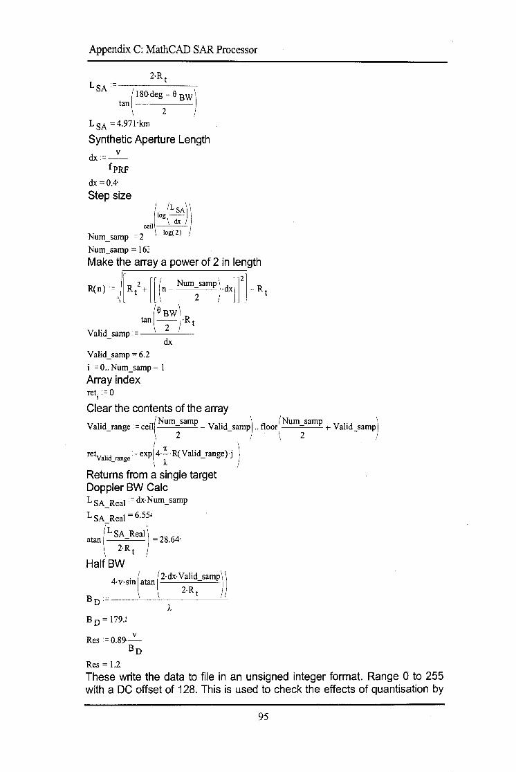
Appendix C: MathCAD SAR Processor
2·Rt LsA =-------
( 180deg - 9 BW)
tan-----2
LsA =4.971-lan
Synthetic Aperture Length
dx:=_v_
fpRf
dx=0.4·
Step size
ce1l -'------'-.(log(L!A))
Num _ samp =2 log(Z) Num_samp = 16~
Make the array a power of 2 in length
R(n) ~ [ R/ + [[ (n _ Num2smnp) dx]]' ]- Rt
tan(e BW:·R . 2 t
Vahd_ samp = --'----'-dx
Valid_samp = 6.2
i = 0 .. Num_samp - I
Array index ret. := 0
I
Clear the contents of the array
V l.d .1(Num samp V l"d ) fl (Num samp . ) a 1 _range:= cet l - a 1 _samp .. oor l + Vahd_samp
retv I'd = exp(4·.'.'...·R(Valid range)·j ) a 1 _range A. -
Returns from a single target Doppler BW Cale L SA Real = dx·Num_samp
L SA Real= 6.55•
atan (L SA_Real \ = 28.64· 2·Rt )
Half BW
Bn
4·v·sin(atan (2·dx·Valid_samp)) _ 2·Rt
BD = 179.:
Res · = 0.89'~ Bn
Res= 1.2
These write the data to file in an unsigned integer format. Range 0 to 255 with a DC offset of 128. This is used to check the effects of quantisation by
95
Appendix C: MathCAD SAR Processor
allowing the VHDL model to process the data, instead of the MathCAD Simulation WRITEPR.l'{Datal) = 128+ floor( Re( 127·re\))
WRITEPR.l'{DataQ) = 128+ floor( rm( 127·reti))
First we must presum the return by 3 PS_Fact =3
PSNum_samp = floor(Num_samp) PS Fact
Number of samples after presumming PSNum_samp = 54t
a =O .. PSNum_samp- 1
PSi =O .. PSNum_samp- 1
ps _ ret a = tmp~ 0
for ie O .. PS Fact- 1
tmp<- tmp + ret(PS Fact·a+ i)
tmp
And now for the FIR filter filter•= READPRJI{ t64)
Filt_Ien = length (filter)
Filt_Ien = 64
left = ceil( Filtllen)
left= 32
Finds the midpoint of the filter
right =floor( Filt2 len)
right= 32
index =left .. PSNum_samp- right
filt_re~Si • = 0
tilt ret d = tmp<-- 0 - m ex for i e - (left - 1) .. right
tmp~tmp+ filter(left- J)+(ps_ret(index+i)-1
tmp
3 Now we put in a skip factor. This should not be greater than the filter length to avoid data loss Skip_ factor = 4
ceil(log ( p~:::~::p)) Num_samp = 2 log( 2)
Num_samp = 20~
New number of samples after presumming and prefiltering j =O .. Num_samp- 1
. d ·=o PSNum_samp _ 1 Ill ... ----Skip_ factor
96

Appendix C: MathCAD SAR Processor
reduced ret . = 0 - J
Setting the new array to zero in case old data is left there reduced ret . d = tilt reLk. f; . d - m - :> 1p_ actorm
length (reduced _:_ret ) = 2.0·
-1~--~-----'-
o 1000 2000
Filtered return shown in azimuth. Note that the FIR filter has nulled all but the center of the return - that which is low frequency. Now calculate the matched filter
m~ = reduced_ret (Num_samp- (j + l))
length (mt) = 2.0·
k =Num_samp .. 2·Num_samp- 1
I = 0 .. 2·Num_samp- 1
3000 4000
index
5000 6000
Padding for the convolution must be added to avoid wrap around problems m\ =O
reduced _ret k = 0
Time for the FFT's! freq mf • = cfft( mt)
FFT the matched filter freq red ret = cfft( reduced_ ret )
FFT the radar return freq conv =freq red ret ·freq mf
l - l 1
The convolution in the time domain is equivalent to multiplication in the frequency domain
1000 2000
I
Upsampling time to make prettier images
97
3000 4000 5000
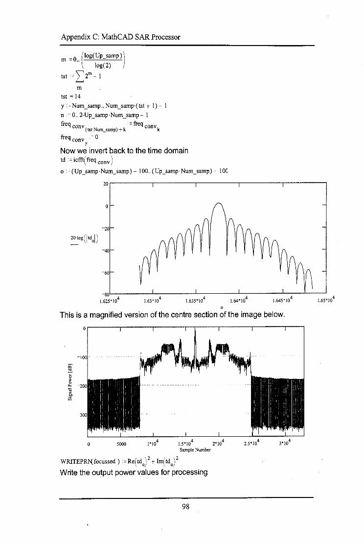
Appendix C: MathCAD SAR Processor
m =O .. (log(Up_samp)) log(2)
tst = L2m - 1
m
tst = 14
y .=Num_samp .. Num_samp·(tst + 1)- 1
n = 0 .. 2·Up_samp·Num_samp- 1
freq conv · = freq conv (tst·Num_samp)+k k
freq conv = O y
Now we invert back to the time domain td = icfft( freq conv)
o = (Up_samp·Num_samp)- 100 .. (Up_samp·Num_samp) + lOC
20
0
-20
20· log ( ltd0
1)
-40
-60
-so 1.625°10
4 1.63"10
4 1.635°10
4
0
1.645"104
This is a magnified version of the centre section of the image below.
0
0 5000 2.5°104
Sample Number
WRITEPRNJocussed ) =Re( td 0
) 2 + Im( td
0)
2
Write the output power values for processing
98
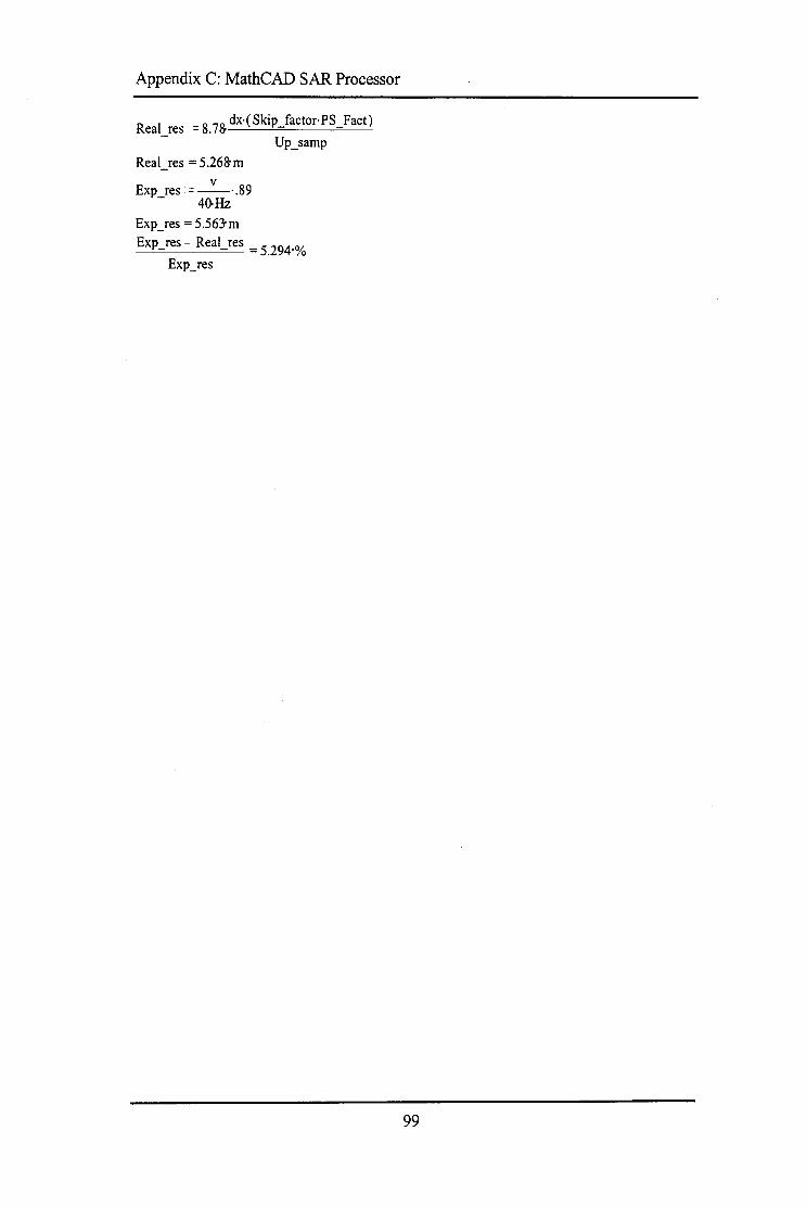
Appendix C: MathCAD SAR Processor
R I 8 70 dx·( Skip factor· PS Fact) eares=.a - -
- Up_samp
Real_res = 5.268-m
v Exp res : = --·.89
- 40-Hz
Exp_res = 5.563-m
Exp_res- Real_res =5
_294.%
Exp_res
99
------------~---------------------------------
Appendix D: VHDL Code Description
Appendix D: VHDL Code Description
This appendix will explain the VHDL code listings found on the enclosed
CD-ROM. For the presummer and prefilter there are each three models: the
algorithm model, the functional model and the synthesis model. Testbenches for the
latter two models are also included as well as some code to create a set of test data.
A number of components were written for the presummer and prefilter. These
included registers, latches and components that calculated the absolute value of
numbers. The testbenches required a RAM model that was written and is also
described below.
All of the code used was VHDL '93 compliant and is incompatible with VHDL '87
because of the file handling routines used.
D.1 Test Data Generator
Filename: FILEGEN.VHD
Description: This code creates a set of test data that can be used by the presummer
for verification. The program simply loops through the values 0 to 255 for each
PRI. A total of 100 PRis are output, each containing 4096 range bins. This simple,
repetitive data was chosen to aid debugging, especially for the prefilter. The output
file was in ASCII format it ease debugging.
D.2 RAM Model
Filename: FUNClOBIT.VHD
Description: The data for the RAM structure was taken from [7]. The RAM model
stores all the data in a single 128K array of integers. The range of the integers is set
to limit the data values to 10 bit precision. Cypress do not produce a 10 bit device
but for simulation purposes it was decided to make a 10 bit device instead of using
two 8 bit devices. This was done to improve the simulation speed.
100
Appendix D: VHDL Code Description
The first two processes ("CounterL" and "CounterR") are responsible for handling
the address lines. Since the device is dual ported, the two ports are designated as
being the left or right port. Separate processes are used for the left and right address
signals as they operate off separate clocks. Every time the address strobe is made
active, the value on the address bus is latched. If the internal address counter is
enabled, this latched address is incremented every clock cycle. The address is reset
to zero when the counter is reset.
The "Memory" process performs all the memory reads and writes. This process
operates on both the left and right ports as only a single process can drive any one
signal. The memory array is declared as a signal. This process is not clocked as all
the inputs to it are clocked - hence the process is still synchronous.
The remaining processes ("RegsL" and "RegsR") are used to register the control
signals. The remaining code implements multiplexers which are required to make
use of extra latches when the RAM is used in pipeline mode.
D.3 Presummer Code
D.3.1 Algorithm Model
Filename: PS ALG.VHD
Description: This code contains a single process. It has no testbench associated
with it as it is the top level simulation. The results need to be verified by hand so
that they can be used for testing the less abstract models.
The model makes use of an array of 4096 integers to hold temporary data while the
PRis are being summed. The data values are constrained to the integer equivalent of
10 bits to ensure that there is no overflow.
One process is used to perform all the processing. The input files are first opened
and the presum counter is reset. A loop is then used to read in an entire PRI. If the
presum counter is zero, the input data is simply stored in the array. If not, it is added
to the contents of the array. When the third PRI is summed, the result of each range
101
Appendix D: VHDL Code Description
bin is written to the output file. Once each PRI has been processed, the presum
counter is incremented. After three PRis have been processed, the presum counter is
reset.
D.3.2 Functional Model
Filename: PS.VHD
Description: The representation of the data values within the presummer is all
integers. This was done to increase the level of abstraction within the model. The
advantage of this was the availability of mathematical functions for integer data
types.
The first block ("SyncFifoWEnl_n") is used for creating a single pulse which is
one clock cycle in length. This is required as the ADCv _ n signal is active for more
than one clock cycle. Since the FIFO is synchronous, more than one sample would
be written ifthe Write Enable signal was not synchronised.
The next block ("Latches") contains the registers for the inputs and outputs. The
adder process that follows it performs the additions which are required for
presummmg.
The "StateMachine" block has a number of processes that define the state machine
behaviour. The states are enumerated and two signals are defined for the current and
next states. The state machine encoding style was unimportant in this model as
during the functional simulation, no timing constraints were imposed on the model.
The first process is used to assign the next state to the current state on each clock
cycle. The second process is used to determine the state transitions while the
remaining processes use the value of the current state to set their outputs. One
process is responsible for the RAM signals, another for the FIFO signals while the
last process controls the internal control signals.
D. 3. 3 Synthesis Model
Filename: PRESUMMER.VHD
Description: This is the code which was used for the synthesis of the presurnmer.
102
Appendix D: VHDL Code Description
The first components which were instantiated were the LUTs to remove the DC
offset. The I and Q channels each had a dedicated LUT. Both the input and output
of the LUTs were registered which meant that the result from the LUT was
available after two clock cycles. To ensure that the FIFO data and RAM data were
available at the same time, a register was inserted into the RAM data path. This was
to hold the RAM data while the LUTs performed their operations on the FIFO data.
The next two blocks ("SyncHBRSel" and "SyncFifoWEnl_n") are used to create a
single pulse every time the HBRSel and FIFOWEnl_n signals respectively go
active. The pulse generated lasts for one clock cycle. Two flip flops are used in this
process.
The "Latches" block contains the instantiations of all the registers. The first two
registers are the RAM data registers described above. The RAM address is also
registered. The reason for this is to make use of the registers in the 1/0 blocks of the
FPGA. This decreases the clock-to-output time on the address signal. The chip
enable signal is also registered.
The "Counters" block contains the instantiations of the counters. As described in
Chapter 7: Presummer Design, four counters were required: Two range bin counters
("ColCounterR" and "ColCounterW"), a range line counter ("RowCounter") and a
presum counter ("PresumCounter"). The presum counter
The "Adders" block contains the instantiations of the adders. Only a single pipeline
stage was used. This was done to decrease the latency of the system as only a single
sample would be processed at a time. The adders were 10 bits wide, although the
input from the LUTs was 8 bits wide. This input was therefore sign extended to 10
bits.
The "StateMachine" block holds the descriptions of the state machine. One Hot
Encoding is used and an index is declared for each state to allow for the
enumeration of the states. The first two processes perform the state transitions while
the remaining processes in the block are responsible for controlling internal and
external signals. Notice should be taken of the "IF" statements used in the output
103

Appendix D: VHDL Code Description
processes. These were used to prevent any comparators from being synthesised.
This increased the operating speed of the state machine.
D.3.4 Presummer Testbench
Filename: TB PS.VHD
Description: The presummer testbench instantiates the presummer and the RAM
and connected the two components. The first two processes create the clock signals
for the two components. The "Timingcard" process creates the external signals
which are input to the presummer (HBRSel and ADCv _ n signals).
The "FifoProc" and "FifoReads" processes provide the functionality of the input
FIFOs. The first process keeps track of the number of samples which are stored in
the FIFO and sets the FIFO empty and full flags accordingly. The second process
reads the input data from disk every time a read operation is requested by the
presummer. In this way, the sampled data from the ADCs can be simulated.
The "OutputData" process makes use of the right hand port of the dual ported RAM
to write the presummed data to disk. Every time the presummer asserts the
PSRowDone line to signal that a presummed line has been written to RAM, the
process reads another PRI from the RAM which is then written to disk. The process
contains counters which operate in the same way as those in the presummer so that
the correct RAM addresses can be produced. By making use of the second RAM
port, the testbench does not interfere with the operations performed on the RAM by
the presummer.
D.4 Prefilter Code
D. 4.1 Algorithm Model
Filename: PF ALG.VHD
Description: This code contains a single process. It has no testbench associated
with it as it is the top level simulation. The results need to be verified by hand so
that they can be used for testing the less abstract models.
104

Appendix D: VHDL Code Description
The model makes use of a 2 dimensional array of 4096 x 99 integers to store the
data to be prefiltered. A second array of 32 integers contains the coefficients for the
FIR filter. The precision of the data is 23 bits while filter coefficients are 8 bits
wide.
One process is used to perform all the processing. The input files are first opened
and the contents are read into the data array. This model only processes the first 100
PRis of a data file. The number can be increased by changing the loop variables and
dimensions of the data array. A second loop is then used to perform the prefiltering.
The result is divided by the correct scale factor and the result is written to disk. A
skip factor of four is introduced before the next set of PRis is processed.
D.4.2 Functional Model
Filename: PF.VHD
Description: The representation of the data values within ·the prefilter is all
integers. This was done to increase the level of abstraction within the model. The
advantage of this was the availability of mathematical functions for integer data
types.
The "FIRFilter" block implements the FIR filter. An array of 32 integers holds the
data to be filtered. On each clock edge, the value on the RAM data bus is clocked
into the filter. This data is multiplied by the coefficients and the result is divided by
the scale factor.
"PSRowCntProc" is a procedure that implements the presummed row counter. The
counter increments when the presummer makes the "PSRowCntlnc" line active.
When the prefilter makes the "DownCounterEn" line active, then the counter
decrements. When both "PSRowCntinc" and "DownCounterEn" and are active, the
counter does nothing.
The "StateMachine" block is similar to those descibed in the presummer above.
Two processes specify the state transitions while the remaining processes control
the outputs and internal control signals.
105

Appendix D: VHDL Code Description
D.4.3 Synthesis Model
Filename: PREFIL TER.VHD
Description: This is the code that was used for synthesising the prefilter. The top
level of the design was actually a schematic description so that the FIR filter,
written in AHDL, could be linked to the VHDL description of the remaining
hardware. The VHDL source code is divided into three main blocks:
"PostProcessing", "Counters" and "StateMachine".
The "PostProcessing" block provides all the numerical processing on the data once
it has been FIR filtered. Two registers ("FIROutputRegI" and "FIROutputRegQ")
are used to latch the correct output from the FIR filter since the filter output is
continuous. The state machine controls the register enable signal
(''LatchFIRDataEn'').
Two absolute value components then process the FIR filter output. These
components check the MSB of the incoming data to determine whether the value is
positive or negative. Two's complement representation is assumed. If the data is
negative, the bits which represent it are inverted and added to 1. If the data is
positive, it is merely output. Three pipeline stages were used in the adder. More
pipeline stages could have been added if the component was too slow but this was
not required.
A pair of dividers is instantiated to divide the absolute value of the FIR filter data.
Since this was the slowest part of the circuit, the maximum amount of pipelining
was introduced (seven stages). The limit on the number of pipeline stages was .
specified by the component.
Two pairs of LUTs were required to add the required DC offset - one for positive
values and the other for negative values. The outputs of these LUTs were
multiplexed so that correct output would be placed on the FIFO data bus. The
selection signal for this multiplexer was the MSB of the register that latched the FIR
filter output.
106
Appendix D: VHDL Code Description
The "Counters" block holds all the address and state machine counters.
"SampleCounter" and "BinCounter" are the PRI and range bin counters
respectively. They are used for generating the RAM address. "StartCounter"
contains the start value of the PRI counter which is reloaded after every range bin
has been processed. "StartCounter" is only 4 bits wide while "SampleCounter" is 6
bits wide. The reason for this is that "StartCounter" is required to increment in
multiples of four. When connected to the PRI counter, the two LSBs are therefore
connected to ground.
The width of "BinCounter" is 13 bits instead of the expected 12 bits required to
represent 4096 values. The reason for this is that the state machine uses the MSB as
the signal to indicate when an entire PRI has been processed. The MSB of the
counter is high after 4096 increments. To enable future support for 4096 or 2048
range bins, the two MSBs of the "BinCounter" are connected to a multiplexer. The
selection signal ("Bins4096n2048") is used to control the number of range bins per
PRI. This signal is pulled high internally as it was not required in this
implementation. A simple modification would be required to route this signal to an
input pin.
"PSRowCounter" is used to track the number of presummed rows in memory. The
"DownCounter" is used to count four clock pulses which will decrement the
"PSRowCounter" by four, after each PRI has been processed. The "FIRCounter" is
used to count the number of samples that are written into the FIR filter.
The "StateMachine" block is similar to those used in the models above. The first
two processes control the state transitions while the remaining processes control the
internal and external signals.
The two signals "WriteDataNow" and "LatchDataNow" decode the outputs of
"FirCounter" and indicate to the state machine when to latch the FIR filter output
data and when to write the processed output to the FIFOs.
D.4.4 Prefilter Testbench
Filename: TB PF. VHD
107

Appendix D: VHDL Code Description
Description: The pre:filter testbench instantiates the prefilter and the RAM and
connects the two components. This testbench operates in the reverse order to the
presummer testbench. The data is first written to the RAM through the right hand
port from disk. Once the prefilter has filtered the data, it writes it to output FIFOs
which are simulated in the testbench. The output data is written to disk.
The "fuputData" process is responsible for loading the RAM with the presummed
data. One sample is loaded per clock cycle until an entire range line has been
loaded. The testbench then waits for the remainder of the PRI and then loads the
next range line. After every range line has been written, the testbench asserts the
"PSRowCntfuc" input for one clock cycle.
The "OutputData" process simulates the behaviour of the output FIFOs. Each time a
write operation is requested, the testbench writes the data on the FIFO data bus to
disk.
108

REFERENCES
1. Altera, FIR Filters, Functional Specification l, Version 1, Altera Corporation,
1996.
2. Altera, Implementing FIR Filters in FLEX Devices, Application Note 73,
Version 1.01, Altera Corporation, 1998.
3. Altera, State Machine Encoding, Application Brief No. 131, Altera
Corporation, 1994.
4. Anderson A.H., Downs G.S., Shaw G.A., RASSP Benchmark -1 and -2:
Preliminary Assessment, 2nd RAS SP Conference
http ://rassp .aticorp .orglpublic/ confs/2nd/ anderson. pdf, 1995
5. Andraka R., Multiplication
http://users.ids.net/-randraka/multipli.htm, 1998.
m FPGAs,
6. Baluja S., Population-Based Incremental Leaming: A Method for Integrating
Genetic Search Based Function Optimisation and Competitive Learning,
http://www.cs.cmu.edu/afs/cs/user/baluja/www/papcrs/CMU-CS-94-
163.ps.QZ, 2 June 1994.
7. Cypress, CY7C09099 Data Sheet, http://www.cypress.com, 1997.
8. Rabine S., VHDL Models for Board-level Simulation, IEEE Design and Test
of Computers, Fall 1996, pp 66-78.
9. Harris F.J., On the use of windows for harmonic analysis with the Discrete
Fourier Transform, IEEE Proceedings, vol. 66, no. 8, 1 January 1978, pp. 51-
83.
10. Myers C., Fiore P., Letellier J.P., Rapid Development of Signal Processors
and the RASSP Program, IEEE International Workshop in Rapid System
109

Prototyping, http://rassp.aticorp.org/public/sanders/rassp-program.pdt: June
1994.
11. Navabi Z., VHDL Analysis and Modelling of Digital Systems, Second
Edition, McGraw-Hill, 1998.
12. Oppenheim A.V., Schafer R.W., Discrete-Time Signal Processing, Prentice
Hall International Inc., 1989.
13. Pridmore J.S., Schaming W.B., RASSP Methodology Overview, 1st RASSP
Conference, http://rassp.scra.org/public/confs/lst/PRIDMORE94A.PDF,
1994.
14. RASSP Taxonomy Working Group, RASSP VHDL Modelling Terminology
and Taxonomy,
http://wvvw.atl.extemal.lmco.com/rassp/taxon/rassp taxon.html, June 1998.
15. Richards M.A., The Rapid Prototyping of Application Specific Signal
Processors (RASSP) Program: Overview and Status, 1st RASSP Conference,
http://rassp.scra.org/public/confs/lst/rassp-overview.pdf, 1994.
16. Selesnick I.W., Lang M., Barrus C.S., Constrained Least Square Design of
FIR Filters Without Specified Transition Bands, IEEE Trans. on Signal
Processing, vol. 44, no. 8, August 1996, pp. 1879-1892.
17. Shaw G.A., RASSP Benchmark Program Overview, 1st RASSP Conference,
http://rassp.scra.org/public/confs/lst/bmoverview.pdf, 1994.
18. Texas Instruments, IEEE Std 1149.1-1990 (JTAG) Testability,
http://www.ti.com/sc/docs/jtag/jtaghome.htm, 1997.
19. Tremeac Y., Inggs M.R., An example of rapid prototyping on the
TMS320C80 multimedia video processor (MVP), Proceedings of the South
African Symposium on Communications and Signal Processing, September
1998, pp 233-237.
110

20. Xilinx, The Programmable Logic Data Book, Xilinx Inc., 1998.
111
BIBLIOGRAPHY
• Drieling R., Processes and Experiences in VHDL Top Down Design,
http://rassp.scra.org/public/sanders/vhdl-top-down-desit..111.pdf.
• Fiore P.D., Will E., Edelson G., Herold D., Rapid Prototyping Applied to
Underwater Acoustic Model Research and Development,
http://rassp.scra.org/public/confs/2nd/FIORE95A.PDF, 1995
• Gradient A.J., Madisetti V.K., Aylor J.H., Wilsey D.P., A Paradigm Shift in
Digital System Design Education with Industry Participation, Proceedings of
the American Society for Engineering Education,
http://rassp.scra.org/public/efi'asee fin.pdt~ June 1996
• Rabine S., VHDL Models for Board-level Simulation,
http://rassp.aticorp.org/vhdl/guidelines/BoardLevel.ps.gz, February 1996.
• Hein C., Nasoff D., VHDL-Based Performance Modelling and Virtual
Prototyping, http://rassp.aticorp.org/public/confs/2nd/HEIN95B.PDF, 1994
• Hein C., Pridgen J., Kline W., RASSP Virtual Prototyping of DSP Systems,
http://www.sigda.acm.org/Dac/34dac/papers/l 997 /dac97 /pdffiles/30 2.pdf,
1997.
• Hood B., Viewpoint from a Prime Developer,
http://rassp.scra.org/public/sanders/rassp-viewpoint.pdf, Lockheed Sanders.
• Johnson D., Keeping Your Programmable Logic Design On Track,
http://www.appreview.com/AppSearch/Pdfi'CYPRESS199704.PDF, 3
November 1997.
• Linderman R., VHDL for the Schematic Designer,
http://www.appreview.com/AppSearch/Pd£iSYNARIOl99704.PDF, 3
November 1997.
112
I
_J
l -
• Naval Surface Warfare Center, Naval Air Warfare Center (Aircraft Division),
Naval Research Laboratory, A VHDL Modelling Guide,
ftp://130.l 63.68.l l0/Tirep/Guide/vhdlmg20.zip, 31 January 1995.
• Powell S.R., Cesear T.M., Rapid Design and Exploration of Signal Processing
Systems usmg a VHDL Model Generator Based Paradigm,
http://rassp.aticoro.org/public/confs/2nd/dgdt.pdf: 22 August 1995.
• Pridgen J., Jaffe R., Kline W., RASSP Technology Insertion into the Synthetic
Aperture Radar Image Processor Application,
http://rassp.scra.org/public/atl/piidgen.pdf
• Pridmore J., Advanced Technology Laboratories' Path to 4X Improvements,
http://rassp.scra.org/public/ atl/pridmore.pdf, Lockheed Sanders.
• Scanlan L., Rapid Prototyping of Application-specific Signal Processors
(RASSP), http://rassp.scra.org/public/sanders/scanlan-rassp.pdf.
• Shaw G.A., Zuemdorfer B.W., Ford R.A., Anderson J.C., Anderson A.H.,
RASSP Benchmark 2 Technical Description,
http://11ex.11.mit.edu/llrassp/brn2.ps.Z, 10 August 1995.
• Sinander P., The Usage of VHDL in the European Space Agency,
ftp://ftp.estec.esa.nl/pub/vhdl/doc/UseOfVHDL.ps, 1995.
• Sinander P., VHDL Modelling Guidelines,
http://rassp.aticorp.org/vhdl/guidelines/ModelGuide.ps.gz, September 1994.
• Zuemdorfer B., Anderson J.C., Ford R.A., Anderson A.H., Rocco G.A., Shaw
G.A., RASSP Benchmark 1 Technical Description,
http://llcx.ll.mit.edu/llrassp/bml .ps.Z, 13 December 1994.
• Zuemdorfer B., Shaw G A, SAR Processing for RASSP Application
http://llcx.ll.mit.edu/llrassp/bwz/rasspcon3.ps.Z.
113 /