synthesis, characterization and chemical sensor application - Doria
90
SYNTHESIS, CHARACTERIZATION AND CHEMICAL SENSOR APPLICATION OF CONDUCTING POLYMERS Michał Wagner Laboratory of Analytical Chemistry Process Chemistry Centre Department of Chemical Engineering Åbo Akademi University Åbo/Turku, Finland 2013
Transcript of synthesis, characterization and chemical sensor application - Doria
SYNTHESIS, CHARACTERIZATION AND
CHEMICAL SENSOR APPLICATION OF
CONDUCTING POLYMERS
Michał Wagner
Laboratory of Analytical Chemistry Process Chemistry Centre
Department of Chemical Engineering Åbo Akademi University
Åbo/Turku, Finland
2013
Michał W
agner SYN
THESIS, CHARACTERIZATION
AND CHEM
ICAL SENSO
R APPLICATION
OF CO
NDU
CTING
POLYM
ERS 2013
ISBN 978-952-12-2977-0Painosalama Oy – Turku, Finland 2013
SYNTHESIS, CHARACTERIZATION AND
CHEMICAL SENSOR APPLICATION OF
CONDUCTING POLYMERS
Michał Wagner
Laboratory of Analytical Chemistry Process Chemistry Centre
Department of Chemical Engineering Åbo Akademi University
Åbo/Turku, Finland
2013

Supervisors
Professor Carita Kvarnström
Laboratory of Materials Chemistry and Chemical Analysis University of Turku
Professor Ari Ivaska
Laboratory of Analytical Chemistry
Åbo Akademi University
Professor Johan Bobacka
Laboratory of Analytical Chemistry Åbo Akademi University
Reviewer
Professor Csaba Visy
Institute of Physical Chemistry University of Szeged
Hungary
Reviewer and Opponent
Professor Alexander Kuhn
Institute of Molecular Sciences University of Bordeaux
France
ISBN 978-952-12-2977-0 Painosalama Oy – Turku, Finland 2013

I
Preface
The research work summarized in this thesis was mainly carried out at the Laboratory of
Analytical Chemistry of Åbo Akademi University. I would like to thank the following institutions
for financial support: Graduate School of Materials Research, National Graduate School in
Nanoscience, Research Foundation for Åbo Akademi, The Finnish Funding Agency for
Technology and Innovation, Academy of Finland and Australian National Fabrication Facility.
For the scientific support and the opportunity to study at Åbo Akademi, my three supervisors
are gratefully acknowledged. Carita, Ari and Johan, tack så mycket! for your suggestions and
many discussions that lead to the interesting findings shown in this work. Also I would like to
thank all the co‐authors of my scientific articles for their contributions as well the reviewers of
my thesis (Prof. Csaba Visy and Prof. Alexander Kuhn) for having patience to evaluate this
work.
Special thanks for my friends in Åbo! You have made my stay in Finland really joyful. Thank
you! Grzesiek, Weronika, Dorota, Patrycja, Ting Ting, Ulrrika, Neg, … and this list could
continue forever!
Finally, I want to thank my beloved family. Dziekuję wam za bezgraniczne wsparcie i miłość!!!
This work is dedicated to you.
Åbo, October 2013
“Per Aspera ad Astra”
II
Abstract
Polymeric materials that conduct electricity are highly interesting for fundamental studies and
beneficial for modern applications in e.g. solar cells, organic field effect transistors (OFETs) as
well as in chemical and bio‐sensing. Therefore, it is important to characterize this class of
materials with a wide variety of methods. This work summarizes the use of electrochemistry
also in combination with spectroscopic methods in synthesis and characterization of
electrically conducting polymers and other π‐conjugated systems. The materials studied in this
work are intended for organic electronic devices and chemical sensors. Additionally, an
important part of the presented work, concerns rational approaches to the development of
water‐based inks containing conducting particles.
Electrochemical synthesis and electroactivity of conducting polymers can be greatly enhanced
in room temperature ionic liquids (RTILs) in comparison to conventional electrolytes.
Therefore, poly(para‐phyenylene) (PPP) was electrochemically synthesized in the two
representative RTILs: bmimPF6 and bmiTf2N (imidazolium and pyrrolidinium‐based salts,
respectively). It was found that the electrochemical synthesis of PPP was significantly
enhanced in bmimPF6. Additionally, the results from doping studies of PPP films indicate
improved electroactivity in bmimPF6 during oxidation (p‐doping) and in bmiTf2N in the case of
reduction (n‐doping). These findings were supported by in situ infrared spectroscopy studies.
Conducting poly(benzimidazobenzophenanthroline) (BBL) is a material which can provide
relatively high field‐effect mobility of charge carriers in OFET devices. The main disadvantage
of this n‐type semiconductor is its limited processability. Therefore in this work BBL was
functionalized with poly(ethylene oxide) PEO, varying the length of side chains enabling water
dispersions of the studied polymer. It was found that functionalization did not distract the
electrochemical activity of the BBL backbone while the processability was improved
significantly in comparison to conventional BBL.
Another objective was to study highly processable poly(3,4‐ethylenedioxythiophene)
poly(styrenesulfonate) (PEDOT:PSS) water‐based inks for controlled patterning scaled‐down to

III
nearly a nanodomain with the intention to fabricate various chemical sensors. Developed
PEDOT:PSS inks greatly improved printing of nanoarrays and with further modification with
quaternary ammonium cations enabled fabrication of PEDOT:PSS‐based chemical sensors for
lead (II) ions with enhanced adhesion and stability in aqueous environments. This opens new
possibilities for development of PEDOT:PSS films that can be used in bio‐related applications.
Polycyclic aromatic hydrocarbons (PAHs) are a broad group of π‐conjugated materials
consisting of aromatic rings in the range from naphthalene to even hundred rings in one
molecule. The research on this type of materials is intriguing, due to their interesting optical
properties and resemblance of graphene. The objective was to use electrochemical synthesis
to yield relatively large PAHs and fabricate electroactive films that could be used as template
material in chemical sensors. Spectroscopic, electrochemical and electrical investigations
evidence formation of highly stable films with fast redox response, consisting of molecules
with 40 to 60 carbon atoms. Additionally, this approach in synthesis, starting from relatively
small PAH molecules was successfully used in chemical sensor for lead (II).

IV
Referat
Elektriskt ledande polymerer är mycket intressanta material både med tanke på fundamental
forskning och moderna tillämpningar t.ex. i solceller, organiska transistorer (OFET) samt i
kemiska och biosensorer. Därför är det mycket viktigt att karakterisera dessa material med
olika analytiska tekniker. I detta arbete används elektrokemiska metoder och deras
kombinationer med vissa spektroskopiska metoder för karakterisering av elektriskt ledande
polymerer och andra π‐konjugerade system. Material som har studerats i detta arbete finner
användning närmast i organiska elektroniska komponenter och kemiska sensorer. I detta
arbete behandlas ytterligare utveckling av ett vattenbaserat bläck som består av elektriskt
ledande polymerer.
Elektrokemisk syntes av ledande polymerer kan också utföras i joniska vätskor vid
rumstemperatur (RTIL) i vilka ledande polymerer generellt även har funnits visa höjd
elektroaktivitet. Därför studerades elektrokemisk syntes av poly(parafenylen) (PPP) i två olika
joniska vätskor: bmimPF6 och bmiTf2N (på imidazolium och pyrrolidinium baserade salter).
Elektrokemisk syntes av PPP i bmimPF6 förbättrades avsevärt jämförd med syntes i organiska
lösningsmedel. Då dopningsreaktioner av PPP studerades i dessa joniska vätskor fann man, att
polymerens p‐dopning i bmimPF6 och n‐dopning i bmiTf2N förbättrades avsevärt. Dessa
resultat kunde bekräftas med in situ IR‐spektroskopiska studier.
Det elektrisk ledande materialet poly(benzimidazobenzofenantrolin) (BBL) visar relativt hög
fälteffekt‐mobilitet av laddningsbärare och kan med fördel användas i OFET‐komponenter.
Nackdelen med BBL som är en n‐typs halvledare är dess begränsade processbarhet. I detta
arbete studerades möjligheten att funktionalisera BBL med olika långa sidokedjor av
poly(ethylenoxid) (PEO). På detta sätt kunde man framställa vattendispersioner av BBL.
Funktionaliseringen påverkade inte BBLs elektroaktivitet med däremot ökade dess
processbarhet avsevärt jämfört med icke‐funktionaliserat BBL.
I detta arbete utvecklades också kompositmaterial av poly(3,4‐etylendioxytiofen)‐
poly(styrensulfonat) (PEDOT:PSS) för användning som ledande bläck. Detta material skulle

V
användas vid framställning av olika kemiska sensorer i nanoskala. Det utvecklade PEDOT:PSS‐
bläcket visade sig ha goda egenskaper för tryckning av nanomönster. Då bläcket modifierades
ytterligare med kvartära ammoniumjoner, kunde man framställa kemiska sensorer för
bly(II)joner. Materialet visade också ökad adhesion till substratet och stabilitet i
vattenlösningar. Detta öppnar nya möjligheter för användning av membraner bestående av
PEDOT:PSS i biologiska tillämpningar.
Polycykliska aromatiska kolväten (PAH) är en bred grupp av π‐konjugerande material som
består av olika antal aromatiska ringar, från naftalen till molekyler som består av flera hundra
ringar. Forskning av dessa material är av stort intresse, inte minst av att de påminner grafen till
sin struktur. Målet med denna del av avhandlingen var att använda elektrokemisk syntes för
framställning av relativt stora PAH‐molekyler som skulle användas i kemiska sensorer.
Spektroskopiska, elektrokemiska och elektriska studier visade att man kunde framställa mycket
stabila membraner med snabba redox‐förlopp. Dessa molekyler bestod av 40 till 60 kolatomer.
Relativt små PAH‐molekyler framställda på detta sätt kunde användas med fördel i kemiska
sensorer för bly(II)joner.

VI
The thesis is based upon the following papers:
I. Michal Wagner, Carita Kvarnström and Ari Ivaska, “Room temperature ionic liquids in electrosynthesis and spectroelectrochemical characterization of poly(para‐phenylene)” Electrochimica Acta, 55 (2010) 2527−2535.
II. Michal Wagner, Anna Österholm, Sami‐Pekka Hirvonen, Heikki Tenhu, Carita Kvarnström and Ari Ivaska, “Characterization of water dispersible n‐type poly (benzimidazobenzo‐phenanthroline) BBL derivitatives”, Macromolecular Chemistry and Physics, 212 (2011) 1567–1574.
III. Michal Wagner, Kai Yu, Carita Kvarnström and Ari Ivaska, “Synthesis and characterization of electroactive films based on benzo(a)pyrene”, Electrochimica Acta, 56 (2011) 3443−3446.
IV. Michal Wagner, Carita Kvarnström, Ari Ivaska and Johan Bobacka, “Electrochemical properties of novel porous carbon based material synthesized from polycyclic aromatic hydrocarbons”, Electrochimica Acta, 105 (2013) 384–393.
V. Grzegorz Lisak, Michal Wagner, Carita Kvanström, Johan Bobacka, Ari Ivaska, and Andrzej Lewenstam, “Electrochemical behaviour of poly(benzopyrene) films doped with eriochrome black T as a Pb2+‐selective sensors”, Electroanalysis, 22 (2010) 2794–2800.
VI. Michal Wagner, Grzegorz Lisak, Ari Ivaska and Johan Bobacka, “Durable PEDOT:PSS films obtained from modified water‐based inks for electrochemical sensors”, Sensors and Actuators B, 181 (2013) 694–701.
VII. Michal Wagner, Cathal D. O’Connell, David G. Harman, Ryan Sullivan, Ari Ivaska,
Michael J. Higgins and Gordon G. Wallace, “Synthesis and optimization of PEDOT:PSS based ink for printing nanoarrays using Dip‐Pen Nanolithography”, accepted manuscript in Synthetic Metals.
Note: all of the papers listed above are re‐printed in the appendix with a permission of the copyright holders.
Contributions of the author:
Papers I and IV. The author performed all the experimental work, evaluated all the results, and wrote the manuscript.
Papers II, V, VI and VII. The author performed the experimental work, evaluated the results, and wrote the manuscript together with the co‐authors.
Paper III. The author evaluated all the results and wrote the manuscript. The experimental work was performed together with the co‐authors.
VII
Table of contents
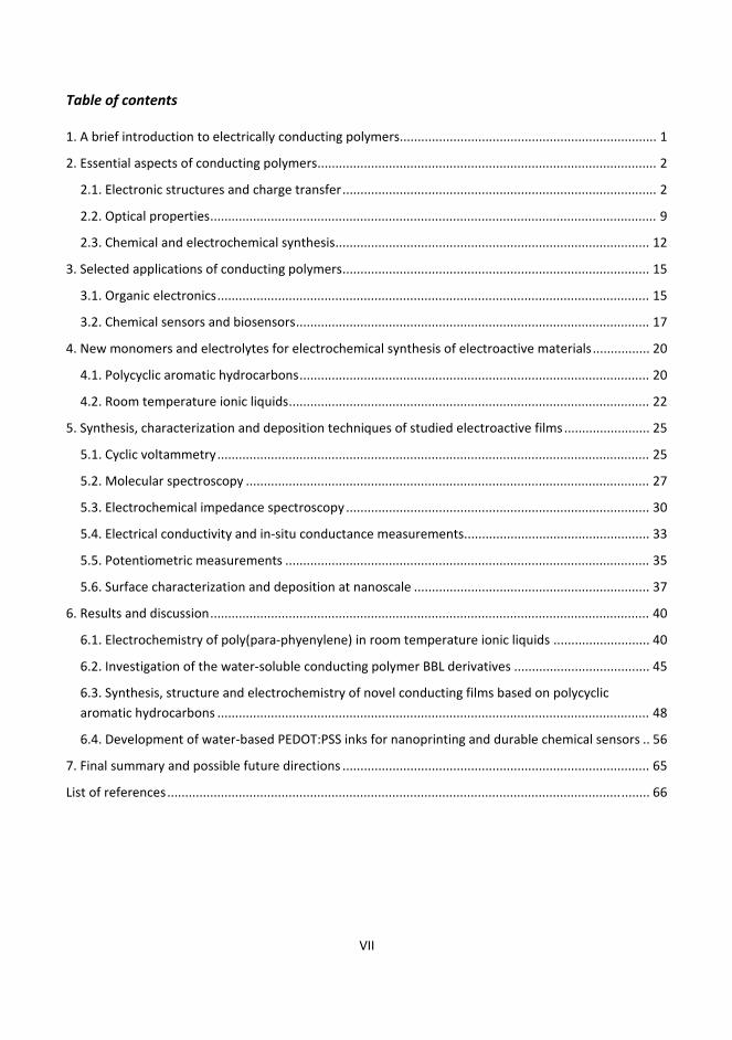
1. A brief introduction to electrically conducting polymers........................................................................ 1
2. Essential aspects of conducting polymers ............................................................................................... 2
2.1. Electronic structures and charge transfer ........................................................................................ 2
2.2. Optical properties ............................................................................................................................. 9
2.3. Chemical and electrochemical synthesis ........................................................................................ 12
3. Selected applications of conducting polymers ...................................................................................... 15
3.1. Organic electronics ......................................................................................................................... 15
3.2. Chemical sensors and biosensors ................................................................................................... 17
4. New monomers and electrolytes for electrochemical synthesis of electroactive materials ................ 20
4.1. Polycyclic aromatic hydrocarbons .................................................................................................. 20
4.2. Room temperature ionic liquids ..................................................................................................... 22
5. Synthesis, characterization and deposition techniques of studied electroactive films ........................ 25
5.1. Cyclic voltammetry ......................................................................................................................... 25
5.2. Molecular spectroscopy ................................................................................................................. 27
5.3. Electrochemical impedance spectroscopy ..................................................................................... 30
5.4. Electrical conductivity and in‐situ conductance measurements .................................................... 33
5.5. Potentiometric measurements ...................................................................................................... 35
5.6. Surface characterization and deposition at nanoscale .................................................................. 37
6. Results and discussion ........................................................................................................................... 40
6.1. Electrochemistry of poly(para‐phyenylene) in room temperature ionic liquids ........................... 40
6.2. Investigation of the water‐soluble conducting polymer BBL derivatives ...................................... 45
6.3. Synthesis, structure and electrochemistry of novel conducting films based on polycyclic
aromatic hydrocarbons ......................................................................................................................... 48
6.4. Development of water‐based PEDOT:PSS inks for nanoprinting and durable chemical sensors .. 56
7. Final summary and possible future directions ...................................................................................... 65
List of references ....................................................................................................................................... 66

VIII
List of abbreviations and symbols
AC alternating current ACN acetonitrile AFM atomic force microscopy ATR attenuated total reflectance A surface area of a WE (cm2) ap activity of the primary ion (M) ai activity of the interfering ion (M) ax1 activity of the primary ion outside a membrane (M) ax2 activity of the primary ion inside a membrane (M) BaP benzo(a)pyrene BBL poly(benzimidazobenzophenanthroline) bmimPF6 1‐butyl‐3‐methylimidazolium hexafluorophosphate bmpTf2N 1‐butyl‐1‐methylpyrrolidinium bis(trifluoromethylsulfonyl)imide B time constant related to diffusion (s1/2) CE counter electrode CPE constant phase element CTA+ hexadecyltrimethylammonium cation CV cyclic voltammetry C capacitance (F) Cdl double layer capacitance (F) cb bulk concentration (mol cm−3) cp concentration of the primary ion (M) ci concentration of the interfering ion (M) DC direct current DNA deoxyribonucleic acid DPN dip‐pen nanolithography DSC dye sensitized solar cell D diffusion coefficient (cm2 s−1) dh density of holes (cm−3) de density of electrons (cm−3) df density of a film (g cm−3) dp penetration depth (in units of length) EbT eriochrome black T EDX energy‐dispersive X‐rays EG ethylene glycol EIS electrochemical impedance spectroscopy E electrical potential (V) Ecell total potential of electrochemical cell/battery (V) E°’ formal redox potential (V) Eox oxidation potential (V) Ered reduction potential (V) Ep peak‐to‐peak separation (V) Eν energy of oscillator (Hz) emf electromotive force (V) FET field‐effect transistor FTIR Fourier transform infrared spectroscopy
IX
F Faraday constant (equal to 96485 C mol−1) fc force constant (N m‐1) GC glassy carbon substrate G electrical conductance (S) HOMO highest occupied molecular orbital IR infrared IRAV infrared active vibration ISE ion‐selective electrode ISM ion‐selective membrane ITO indium tin oxide I electrical current (A) Id intensity of the “d” band Ig intensity of the “g” band Ip peak current (A) It intensity of transmitted light I0 intensity of incident photons J current density (A cm−2) Kp,i selectivity coefficient ks constant number equal to 269000 LUMO lowest unoccupied molecular orbital LED light‐emitting diode LDL lower detection limit (M) La crystallite length (nm) Lb length of the double‐band electrode (cm) Lf film thickness (μm) Ls light path (cm) Lsb length of the half spacing of the double‐band electrode (nm) Mm molecular weight of a monomer (g mol−1) mr reduced mass (kg) n the value in between or equal to 0 and/or 1 (related to CPE) ne number of transferred electrons nn refractive index OSC organic solar cell OTFT organic thin‐film transistor O hyperbolic cotangent diffusion element PA polyacetylene PAH polycyclic aromatic hydrocarbon PANI polyaniline PBP poly(benzopyrene) PC propylene carbonate PEDOT poly(3,4‐ethylenedioxythiophene) PEO poly(ethylene oxide) PF polyfluorene PPP poly(para‐phenylene) PPy polypyrrole PPV poly(para‐phenylenevinylene) PSS poly(styrenesulfonate) PT polythiophene

X
PVC poly(vinyl chloride) QAB quaternary ammonium bromide Q electric charge (C) Qp polymerization charge (C) Qd doping charge (C) qc charge of carrier (C) qp charge number of the primary ion qi charge number of the interfering ion RE reference electrode RTIL room temperature ionic liquid Re equilibrium distance (in units of length) Rf film resistance (Ω) Rp polarization resistance (Ω) Rs solution resistance (Ω) Ŕ ideal gas constant (equal to 8.3144621 J mol−1 K−1) SEM scanning electron microscopy Sn energy level of a singlet state (n = 0, 1, 2, ...) TBA+ tetrabutylammonium cation TBAPF6 tetrabutylammonium hexafluorophosphate TMOA+ trimetyloctylammonium cation TOA+ tetraoctylammonium cation T hyperbolic tangent diffusion element T temperature (K) t time (s) UV‐vis ultraviolet and visible v scan rate (V s−1) vn vibrational quantum numbers (n = 0, 1, 2, ...) WE working electrode W work (J) Y0 magnitude of admittance (S s1/2 or S sn depending on the type of electrical element) Z electrical impedance (Ω) Z’ real part of the impedance (i.e. resistance) (Ω) Z’’ imaginary part of the impedance (i.e. reactance) (Ω)
Greek‐based symbols γf attenuation coefficient (cm−1) γp activity coefficient θ phase angle μh mobility of holes (cm2 V−1 s−1) μe mobility of electrons (cm2 V−1 s−1) σ electrical conductivity (S cm−1) ρ resistivity (Ω cm) χ2 fitting error ω angular frequency (rad s−1)
Note: the metric prefixes for some of the units and their dimensions were chosen arbitrarily.
1
1. A brief introduction to electrically conducting polymers
Until the discovery of the significant increase in electrical conductivity during oxidation of
polyacetylene (PA) with iodine vapor in 1977 [1], all polymers where commonly regarded as
electrical insulators. The first work on truly conducting polypyrrole (PPy) oxidized with iodine
emerged already in 1963 [2], however, this work did not acquire immense attention from the
scientific community. Thus the era of conducting polymers originate from studies on trans‐PA
oxidized with iodine, covering the whole range of electrical conductivity: from insulating state
to metal‐like behavior [1,3]. Due to numerous highly important reports in both fundamental
and applied research, conducting polymers were recognized by the Nobel committee in 2000
[4]. The excitement over conducting polymers can be attributed to the fact that in principle
they constitute a new branch of materials which binds together desired semiconducting
properties with mechanical flexibility and in some cases biocompatibility. Such a highly
practical combination is not observed in metals, inorganic semiconductors or non‐conjugated
saturated polymers. Also, the advent of conducting polymers created new opportunities for
fundamental studies in solid‐state physics and actually this type of materials are another
fascinating crossover of chemistry and physics.
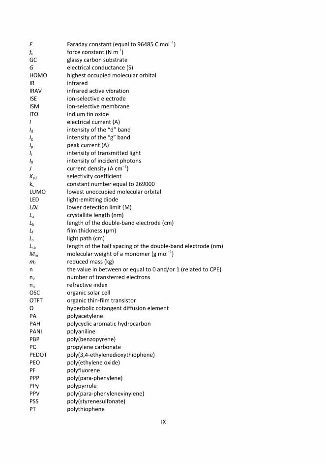
Figure 1. Chemical structures of common conducting polymers.
2
The structure of conducting polymers is usually composed of C, H and heteroatoms like N or S
within a π‐conjugated system. Figure 1 presents the basic chemical structure of some
conducting polymers. Delocalized π‐electrons originate from one unpaired electron per carbon
atom in contrary to saturated polymers where all four valence electrons are used to constitute
covalent chemical bonds. What all conducting polymers have in common is a high π‐electron
overlap along the polymer chain which facilitates the possibility of fast electron transfer.
Despite of that fact, delocalization of π‐electrons along the polymer backbone itself is not
sufficient to obtain high conductivities and a process called doping is needed. Chemically this
process is related to oxidation/reduction of the polymer, resulting in formation of charge
carriers. Importantly the behavior of those charge carriers can be in depth explained by solid‐
state physics. Hence, conducting polymers were also used as model compounds in studying
e.g. electron‐lattice interactions [5] or Mott insulator/metal transition [6]. Since conducting
polymers can easily be chemically or electrochemically doped, it is possible to incorporate ions
into polymer films that can carry desired functionality. This fact facilitated numerous ideas in
designing new devices and real applications e.g. in corrosion science, organic electronics,
energy storage and chemical sensors [7‐10].
2. Essential aspects of conducting polymers
2.1. Electronic structures and charge transfer
In nature, energy that systems possess can be quantized into small portions which can be
visualized as energy levels. In every atom, electrons occupy certain energy levels and they
cannot be found in between the energy gap (difference in two energy states). In other words
electrons can adopt only specific orbitals with specific energies. From the chemical point of
view, important are relations and configurations of electrons from the outermost electron shell
(valence electrons), since they contribute to chemical bonds between atoms. Interactions of
atoms result in formation of molecules and thus the probability of finding an electron in a
specific space‐time domain can be calculated using the concept of molecular orbital. Many
physical and chemical properties of condensed matter can be accurately described by the band
theory of solids. The bands are a visualization of overlapping of many molecular orbitals where
3
energy can be considered as continuous. According to this theory, valence electrons are
statistically attributed to the so‐called valence band and virtually free electrons with higher
energies to the conduction band.
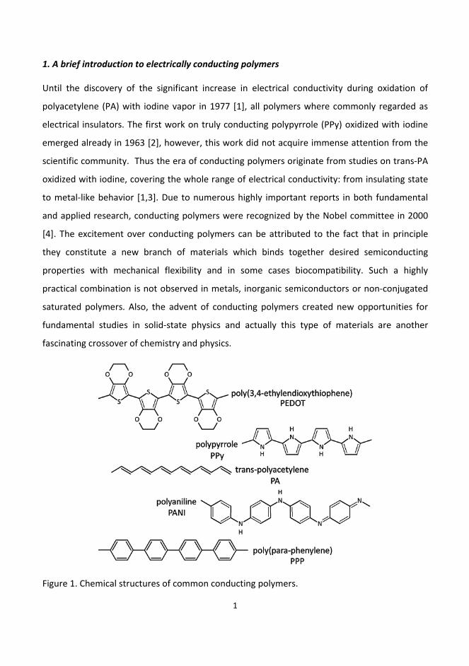
Figure 2. The band structures of three conductivity classes of materials as a function of energy
at 0 K (A). Simplified representation of doping mechanism for inorganic semiconductor shown
as a function of energy (B).
When considering the flow rate of electrons through solid matter, all known materials can be
divided into three groups: insulators, semiconductors and conductors. Those groups can be
interpreted in terms of the band theory yielding satisfactory explanations for many physical
and chemical phenomena. Upon thermal or other excitations, electrons change their state and
“jump” to energy levels with higher quantum numbers. According to Fermi‐Dirac statistics all
electrons are in constant movement even at 0 K and at this temperature will fill all available
energy states below a certain energy level termed the Fermi level. For insulators and
semiconductors at 0 K, the Fermi level appears exactly in between the valence and conduction
bands. What makes a semiconductor different from insulator is the significantly smaller energy
of the band gap of the former. Hence, for a semiconductor at higher temperatures this
threshold energy can statistically be overcome by electrons (extension of Fermi level). In a

4
conductor like metal, valence electrons are essentially free and the conduction and valence
band is merged, and split in half by Fermi level at 0 K. Figure 2 A presents three conductivity
classes according to the band theory and the lowest unoccupied molecular orbital (LUMO) and
the highest occupied molecular orbital (HOMO) also marked in the figure.
Electrical conductivity depends on structural arrangement of matter, i.e. crystalline vs.
disordered systems. For metals which possess crystalline structure the conductivity decreases
with increasing temperature and at high temperatures this relation is linear. This increase in
electrical resistance is mostly due to the scattering of electrons by interactions with phonons
(in this case: thermally induced vibrations of the crystalline lattice). In a simplified view on
semiconductors, the rise in temperature facilitates formation of excited electrons which can
move from the valence band to the conduction band. Hence, the electrical resistance of a
semiconductor decreases exponentially with increasing temperature. The removal of electrons
form the valence band produces virtual charge carriers: electron holes. Hence, the overall
conductivity of a semiconductor is in general, dependent on the charge, mobility and density
of the carriers, according to the following equation:
(1)
Where: σ is the electrical conductivity in S cm−1, qc is the charge of carrier in C. The symbols
μ(h,e) and d(h,e) refer to charge carrier mobility in cm2 V−1 s−1 and density in cm−3, with respect
to holes (h) and electrons (e). As can be seen from equation 1, the mobility of charge carriers in
an electric field, plays a dominant role in the conductivity of semiconductors and with
increasing order the movement of charge carriers can be significantly enhanced.
Both inorganic and organic semiconductors can be doped, creating defects that have influence
on the order of the system. The simplified effect of doping on the electronic structure of an
intrinsic inorganic semiconductor can be seen in Figure 2 B. Insertion of e.g. arsenic or boron
atoms into the crystalline structure of silicon creates defects that can be visualized by an
additional energy level. Doping of silicon with arsenic creates an electron donor level near the
conduction band (left picture in Figure 2 B). Free electrons from an electron donor propagate
5
to the conduction band by passing an energy barrier that is significantly smaller then energy
band gap between the conduction and valence band. Since charge carrier movement is
described by negative electrons this donor doped material is referred to as an n‐type
semiconductor. On the other hand, doping of silicon with boron creates an electron acceptor
level near the valence band (right picture in Figure 2 B). Electrons from the valence band
propagate to the acceptor level which has electron deficiency, leaving positive holes in the
valence band propagating in opposite direction and thus this acceptor doped material is
referred to as a p‐type semiconductor.
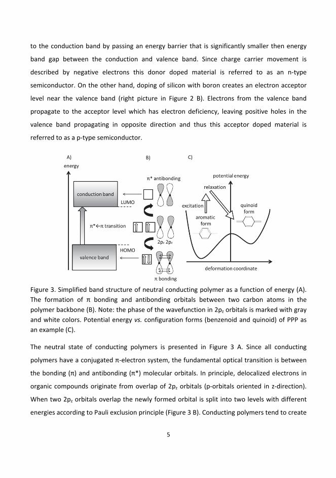
Figure 3. Simplified band structure of neutral conducting polymer as a function of energy (A).
The formation of π bonding and antibonding orbitals between two carbon atoms in the
polymer backbone (B). Note: the phase of the wavefunction in 2pz orbitals is marked with gray
and white colors. Potential energy vs. configuration forms (benzenoid and quinoid) of PPP as
an example (C).
The neutral state of conducting polymers is presented in Figure 3 A. Since all conducting
polymers have a conjugated π‐electron system, the fundamental optical transition is between
the bonding (π) and antibonding (π*) molecular orbitals. In principle, delocalized electrons in
organic compounds originate from overlap of 2pz orbitals (p‐orbitals oriented in z‐direction).
When two 2pz orbitals overlap the newly formed orbital is split into two levels with different
energies according to Pauli exclusion principle (Figure 3 B). Conducting polymers tend to create
6
an amorphous microstructure without long‐range order. Hence, the conjugation range of π
orbitals is limited and a “short” conjugation is specific for conducting polymers resulting in
potential barriers. When additional energy is delivered to the system along the polymer
backbone, an exciton (new state of an electron and hole) is formed. In trans‐PA excitation
leads to formation of new a quasi‐particle that has its electronic state in the middle of the
band gap, termed soliton [11,12]. Physically soliton is an isolated propagating wave that does
not disperse. The formation of solitons in trans‐PA originate from the fact that this conducting
polymer possess two structures with equal energy in the ground state (degeneration). For
other conducting polymers, excitation leads to essentially different chain distortions. An
example of two energetically non‐equal chemical structures of PPP is shown in Figure 3 C: the
stable aromatic structure and the quinoid meta‐stable one with a higher local energy
minimum. After excitation, the polymer relax to the meta‐stable energy states since this
process is relatively faster than relaxation to the aromatic configuration [12]. Such a chain
distortion is equivalent to a quasi‐particle termed polaron which physically is a moving electron
or hole with surrounding deformation. During redox reactions of conducting polymers polarons
or bipolarons are formed.
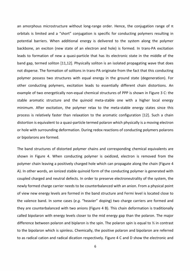
The band structures of distorted polymer chains and corresponding chemical equivalents are
shown in Figure 4. When conducting polymer is oxidized, electron is removed from the
polymer chain leaving a positively charged hole which can propagate along the chain (Figure 4
A). In other words, an ionized stable quinoid form of the conducting polymer is generated with
coupled charged and neutral defects. In order to preserve electroneutrality of the system, the
newly formed charge carrier needs to be counterbalanced with an anion. From a physical point
of view new energy levels are formed in the band structure and Fermi level is located close to
the valence band. In some cases (e.g. “heavier” doping) two charge carriers are formed and
they are counterbalanced with two anions (Figure 4 B). This chain deformation is traditionally
called bipolaron with energy levels closer to the mid energy gap than the polaron. The major
difference between polaron and biplaron is the spin. The polaron spin is equal to ½ in contrast
to the bipolaron which is spinless. Chemically, the positive polaron and bipolaron are referred
to as radical cation and radical dication respectively. Figure 4 C and D show the electronic and
7
chemical structure of a conducting polymer in reduced form. Addition of electrons yields
formation of negative polarons and bipolarons. The negative charges are counterbalanced with
cations. For those systems Fermi level is located close to the conduction band. In analogy to
the oxidized polymer, negative polarons and bipolarons refer to radical anions and radical
dianions, respectively.
Figure 4. Simplified representation of band structures in excited conducting polymers as a
function of energy, together with corresponding chemical structures shown for PPP as an
example. Notes: the direction of gray arrows represents electron spin and white arrows denote
allowed optical transitions.
There are essential differences in conduction and doping mechanisms between organic and
inorganic semiconductors, due to already mentioned absence of long‐range order within π‐
conjugated systems. The absence of long‐range order in organic semiconductors leads to much
lower carrier mobilities in comparison to metals or inorganic semiconductors. Interestingly,
even for the highest reported carrier mobility for polythiophenes (PTs) in field‐effect
transistors the corresponding free path at room temperature of the carrier is lower than the
interatomic distance [13].

8
Figure 5. Schematic representation of localized states in disordered systems as a function of
potential energy (A). Charge carrier hopping to different localized states with different
energies (B) and near Fermi level at temperatures higher than 0 K (C). Schematic picture of
disordered and crystalline regions in conducting polymer (D). Note: the electrical coupling
between crystalline regions is shown with white arrows.
Figure 5 A presents a charge carrier propagating in a disordered system. The periodic potential
energy distribution is disturbed leading to the absence of delocalized wave functions and
formation of localized states (in this case “traps” for the carrier). Essentially, trapped charge
carriers have zero mobility. On the other hand, carriers can “jump” to from one localized state
to another via hopping/tunneling effects. Statistically, carrier can “jump” to the nearest
localized energy states (Figure 5 B). Hopping of a carrier from e.g. state E2 to E1 is easier than
hopping to the state E3, however, both transitions contribute to the rate of carrier jumps. The
“jumps” between localized states can be described by models based on variable range
hopping. In disordered hopping systems localized states are distributed randomly in space and
energetically distributed in accordance with density of states function [14]. In principle, density
of states describes all the states at each energy level that can be potentially occupied. Figure 5
C presents a schematic sketch of random hopping of charge carriers near the Fermi level at
temperatures higher than 0 K. For conducting polymers only the small fraction of dopants
9
leads to charge carriers taking part in the hopping transport in contrary to inorganic
semiconductors, due to the fact that only the localized states near the Fermi level can be
considered. However, the significant increase in dopant concentration leads also to increase in
density of states promoting a higher hopping rate because of the reduced distance between
the localized states.
An overall electrical conductivity of common conducting polymers can be tuned to the range of
102‐103 S cm−1 [15,16]. Such high conductivity values are only approximately two orders of
magnitude lower than for copper at room temperature. The quasi‐metallic behavior of highly
doped conducting polymers cannot be explained by polaron hopping itself, therefore, also
additional mechanisms at microstructure level need to be taken into account. Figure 5 D
presents a schematic picture of microstructure of a disordered conducting polymer. Depending
on the type of conducting polymer, method of synthesis and chain modifications, some parts
of the polymer matrix can be organized into regions with high crystallinity. Crystalline regions
with extended density of states are separated by vast disordered regions rich in localized
states. In principle, charge carriers can propagate from one crystalline region to another
through localized states near the Fermi level via resonance tunneling [17].
Summarizing, the charge transfer mechanism in organic semiconductors and particularly
conducting polymers is of a complicated nature. Electrical conductivity is strictly dependent on
charge carrier mobility and dopant concentration. In contrary to inorganic semiconductors the
carrier mobilities are low and a high concentration of dopant is needed in order to achieve
enhanced electrical conductivity. Propagation of charge carriers (e.g. polarons) in conducting
polymers can be explained by several models which are based on variable range hopping. The
proper understanding of charge transport mechanisms in conducting polymers is highly
beneficial in designing organic electronic and chemical sensor devices.
2.2. Optical properties
Optical properties of materials strictly relate to electronic transitions upon excitation. The
ground (S0) and excited (Sn) states can be considered as potential wells within which the
10
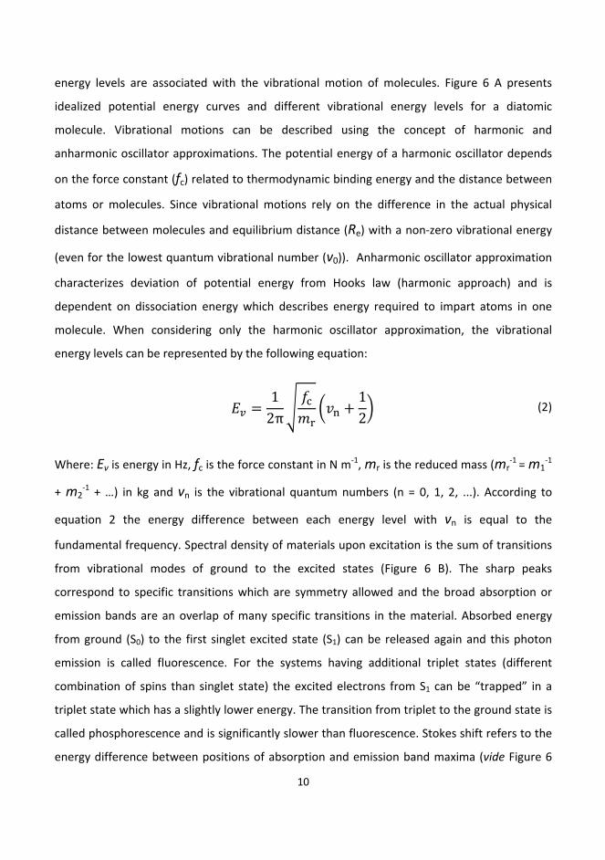
energy levels are associated with the vibrational motion of molecules. Figure 6 A presents
idealized potential energy curves and different vibrational energy levels for a diatomic
molecule. Vibrational motions can be described using the concept of harmonic and
anharmonic oscillator approximations. The potential energy of a harmonic oscillator depends
on the force constant (fc) related to thermodynamic binding energy and the distance between
atoms or molecules. Since vibrational motions rely on the difference in the actual physical
distance between molecules and equilibrium distance (Re) with a non‐zero vibrational energy
(even for the lowest quantum vibrational number (v0)). Anharmonic oscillator approximation
characterizes deviation of potential energy from Hooks law (harmonic approach) and is
dependent on dissociation energy which describes energy required to impart atoms in one
molecule. When considering only the harmonic oscillator approximation, the vibrational
energy levels can be represented by the following equation:
12π
12
(2)
Where: Eν is energy in Hz, fc is the force constant in N m‐1, mr is the reduced mass (mr
‐1 = m1‐1
+ m2‐1 + …) in kg and vn is the vibrational quantum numbers (n = 0, 1, 2, ...). According to
equation 2 the energy difference between each energy level with vn is equal to the
fundamental frequency. Spectral density of materials upon excitation is the sum of transitions
from vibrational modes of ground to the excited states (Figure 6 B). The sharp peaks
correspond to specific transitions which are symmetry allowed and the broad absorption or
emission bands are an overlap of many specific transitions in the material. Absorbed energy
from ground (S0) to the first singlet excited state (S1) can be released again and this photon
emission is called fluorescence. For the systems having additional triplet states (different
combination of spins than singlet state) the excited electrons from S1 can be “trapped” in a
triplet state which has a slightly lower energy. The transition from triplet to the ground state is
called phosphorescence and is significantly slower than fluorescence. Stokes shift refers to the
energy difference between positions of absorption and emission band maxima (vide Figure 6
11
B). This shift in energy is mainly connected with system relaxation, other structural
reorganizations and arrangements can however also contribute to the shift.
Figure 6. Idealized representation of the ground (S0) and first excited (S1) states of a diatomic
molecule vs. potential energy (A). Corresponding optical absorption and fluorescence emission
bands (B).
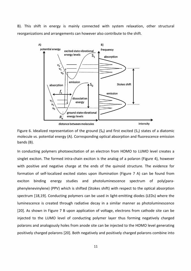
In conducting polymers photoexcitation of an electron from HOMO to LUMO level creates a
singlet exciton. The formed intra‐chain exciton is the analog of a polaron (Figure 4), however
with positive and negative charge at the ends of the quinoid structure. The evidence for
formation of self‐localized excited states upon illumination (Figure 7 A) can be found from
exciton binding energy studies and photoluminescence spectrum of poly(para‐
phenylenevinylene) (PPV) which is shifted (Stokes shift) with respect to the optical absorption
spectrum [18,19]. Conducting polymers can be used in light‐emitting diodes (LEDs) where the
luminescence is created through radiative decay in a similar manner as photoluminescence
[20]. As shown in Figure 7 B upon application of voltage, electrons from cathode site can be
injected to the LUMO level of conducting polymer layer thus forming negatively charged
polarons and analogously holes from anode site can be injected to the HOMO level generating
positively charged polarons [20]. Both negatively and positively charged polarons combine into
12
a singlet exciton and the process of light emission is called electroluminescence. Importantly,
quantum efficiency (the ratio of produced photons to injected charges) for
electroluminescence is significantly smaller than for photoluminescence, due to a loss of 75 %
of electron‐hole pairs to triplet states [21]. The problem in efficiency of LEDs based on PPV
have already been extensively studied and partly overcome by the use of copolymers or bilayer
devices [22,23].
Figure 7. Idealized representation of photoluminescence (A) and electroluminescence (B) in
conducting polymers for singlet excitation radiative decay.
2.3. Chemical and electrochemical synthesis
Chemical activity of any substance is a measure of the ability to undergo chemical reactions.
Vast and extremely versatile chemical reactions can be involved in production of conducting
polymers ranging from classical polymer and organic chemistry methods to electrochemical
polymerization. Additionally, synthetic routes can be assisted with the use of different
catalysts. Selection of a synthetic method depends on the desired application of the
conducting polymer. For fundamental studies of conducting polymers and chemical sensors
fabrication, electrochemical polymerization can be favorable due to its simplicity (one step
synthesis) and a high control over the deposition process. Electrochemical synthesis involves
13
oxidation or reduction of the monomer species in electrolyte solutions to obtain usually
compact films directly on the electrode. Although, electrochemical polymerization is useful in
direct preparation of electroactive films, the major disadvantage of this approach is in
insolubility of the product. From an industrial point of view it is important to study and develop
conducting polymer inks that can be casted, spin coated or deposited on different substrates
to fabricate electronic or sensor devices. Thus, for larger scale production chemical methods
are preferable since they can provide solution processable conducting polymers either in their
undoped or semi‐conducting state.
Electrochemical synthesis can be performed by using different ways of application of the
potential or current to the conducting substrate immersed in an electrolyte containing the
starting monomer. The most simple electrochemical methods used in film preparation includes
potentiostatic or galvanostatic (constant potential and constant current respectively)
polymerization within a two‐ or three electrode system. If the growth of polymer and the
occurring reactions are desired to be monitored then potentiodynamic methods (usually cyclic
voltammetry) are used in a three electrode system. The three electrode set‐up for
electrosynthesis consists of a counter (control of current), a reference (control of potential)
and a working (conducting substrate) electrode, usually abbreviated CE, RE and WE,
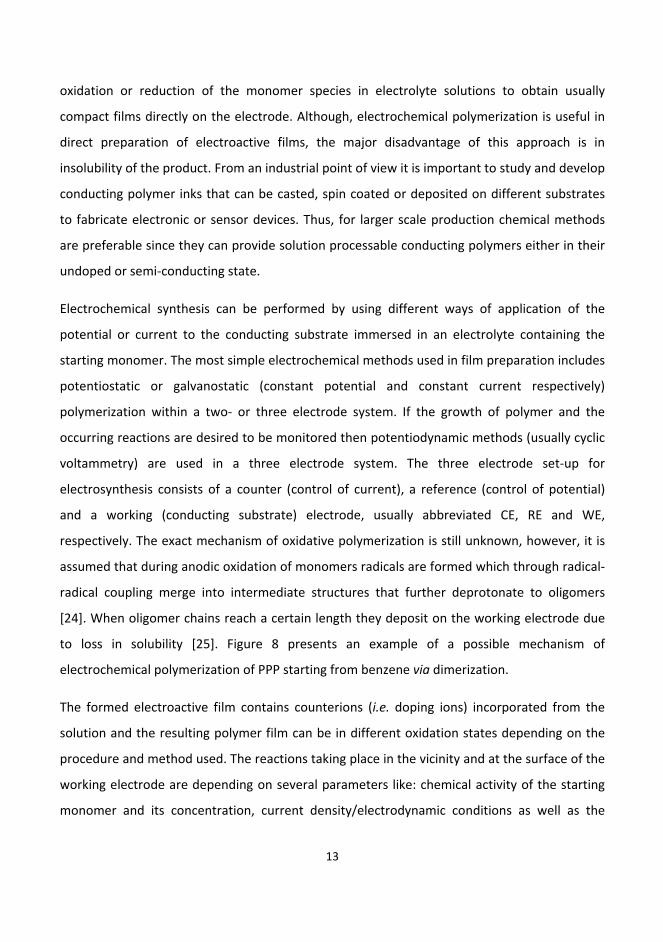
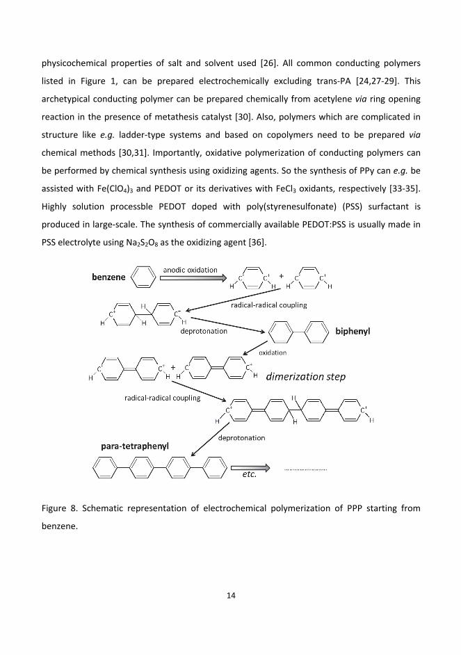
respectively. The exact mechanism of oxidative polymerization is still unknown, however, it is
assumed that during anodic oxidation of monomers radicals are formed which through radical‐
radical coupling merge into intermediate structures that further deprotonate to oligomers
[24]. When oligomer chains reach a certain length they deposit on the working electrode due
to loss in solubility [25]. Figure 8 presents an example of a possible mechanism of
electrochemical polymerization of PPP starting from benzene via dimerization.
The formed electroactive film contains counterions (i.e. doping ions) incorporated from the
solution and the resulting polymer film can be in different oxidation states depending on the
procedure and method used. The reactions taking place in the vicinity and at the surface of the
working electrode are depending on several parameters like: chemical activity of the starting
monomer and its concentration, current density/electrodynamic conditions as well as the
14
physicochemical properties of salt and solvent used [26]. All common conducting polymers
listed in Figure 1, can be prepared electrochemically excluding trans‐PA [24,27‐29]. This
archetypical conducting polymer can be prepared chemically from acetylene via ring opening
reaction in the presence of metathesis catalyst [30]. Also, polymers which are complicated in
structure like e.g. ladder‐type systems and based on copolymers need to be prepared via
chemical methods [30,31]. Importantly, oxidative polymerization of conducting polymers can
be performed by chemical synthesis using oxidizing agents. So the synthesis of PPy can e.g. be
assisted with Fe(ClO4)3 and PEDOT or its derivatives with FeCl3 oxidants, respectively [33‐35].
Highly solution processble PEDOT doped with poly(styrenesulfonate) (PSS) surfactant is
produced in large‐scale. The synthesis of commercially available PEDOT:PSS is usually made in
PSS electrolyte using Na2S2O8 as the oxidizing agent [36].
Figure 8. Schematic representation of electrochemical polymerization of PPP starting from
benzene.

15
3. Selected applications of conducting polymers
3.1. Organic electronics
Conducting polymers and other organic semiconductors have been already intensively studied
for electronic materials. The major research is focused to fabricate organic LED (OLED), field‐
effect transistor (OFET) and solar cell (OSC) devices, opening the “era of plastic electronics”.
Organic electronic devices are usually manufactured in thin‐layer technology (micro‐ and
nanometer scale) by different printing methods utilizing solution processable materials. Hence,
conducting polymer based devices can outdistance “traditional” inorganic technology in
mechanical flexibility, weight and cost to performance ratio.
In the basic form, OLED devices consist of an emissive layer sandwiched between two
electrodes and upon application of electricity light is generated (electroluminescence). The
operating principle of OLEDs can be seen in Figure 7 B. The reason for the great scope on
OLEDs is that they can be used for display manufacturing providing thinner, more efficient and
less power consuming displays than conventional LED or liquid‐crystal technology [37]. In
fabrication of OLED devices, conducting polymers can be used either as an anode or emissive
material or both simultaneously. Among conducting polymers and their derivatives that are
used for an emissive layer are PPVs, PPPs, polythiophenes (PTs) and polyfluorens (PFs) [38‐41].
For application of OLEDs in real displays the important is the proper generation of three basic
colors (red, green and blue) in order to generate the desired color. PPVs and PFs have been
found to provide tunable emission frequencies and relatively high quantum yields. The
emission colors of those polymers span the visible spectrum, however, it was found that PPV‐
based materials are useful as red and green OLEDs and PFs complement with efficient emission
of blue color [42]. A typical anode material for LED devices is indium‐tin‐oxide (ITO) glass
despite its very high surface roughness which causes adhesion problems to organic layers not
desired for flexible electronics [43]. Therefore, there were attempts to exchange ITO with thin
and transparent layers of PEDOT:PSS. Application of this conducting polymer greatly improves
external quantum efficiency and mechanical stability with respect to devices with ITO as the
16
anode material [44]. The major drawback of PEDOT:PSS is its relatively low work function,
which however, can electrochemically be adjusted [45].
Another successful use of conducting polymers in organic electronic devices is in OFETs,
particularly in organic thin‐film transistor (OTFT) devices. Usually an OTFT device consist of
electrical conductors named “source” and “drain” deposited on insulator layer and separated
by a semiconductor. The device is complemented by an additional conducting layer termed
“gate” which is in contact with the insulator. When the voltage is applied between the source
and the gate electrodes current is passing through the semiconductor from source to drain.
Hence, the conductivity is a function of the applied potential. The important parameters of
transistors are ON/OFF ratio and the value of potential needed to induce current flow in the
semiconducting channel. Solution processable organic materials can be used in OTFTs,
reducing the manufacturing cost, providing lower operation voltages and better flexibility in
comparison to inorganic‐based TFTs [46]. The major drawback of OTFT devices is the relatively
low carrier mobilities, affecting the ON/OFF ratio, hence, traditional TFTs will still be used in
applications requiring very high switching speeds [46]. Conducting polymers are used in OTFT
devices either as the semiconductor layer or the electrode material. Frequently used solution
processable polymers in fabricating the semiconducting channel in FETs are PTs and PPVs
derivatives [47‐49]. Importantly, ambipolar transistors (both p‐ and n‐type semiconduction
possible in one device) have been realized by using blends of PPV derivative with
functionalized fullerene or ladder‐type conducting polymer mixed with copper phthalocyanine
dye [50,51]. PEDOT:PSS and PANI conducting polymers can be used for organic source and
drain electrodes, yielding an excellent alternative to the costly metal conductors, especially if
those polymers are exposed to secondary dopants [52,53]. Also, PEDOT:PSS was used to
fabricate an electrochemical transistor where PEDOT:PSS was employed both as the active
switching and source/drain layers [54].
In principle, a solar cell works as a converter of light into electricity. The whole concept of OSC
devices is to some extent an inverted process found in electroluminescent devices (vide Figure
7 B). OSCs are usually made of thin layers of donor and acceptor materials. Incident photons
17
are absorbed by the donor material and the π‐electrons from HOMO level “jump” to LUMO
level, thus excitons are created which diffuse to the donor/acceptor interface and dissociate
into charge carriers. When an exciton reaches this interface the induced electron from LUMO
of donor is then transferred to the LUMO of acceptor layer. Hence, the charge can be
transported to the electrode (e.g. aluminum) generating electricity. The major reason for the
great scope of development of OSCs is the reduction of production costs with respect to
silicon‐based solar cells which require manufacturing in vacuum. In order to practically realize
competitive OSC devices, materials with efficient absorption of light, charge transfer and
separation are needed [55]. The best in overall power conversion efficiency (~11 %) OSC so far,
is the so‐called dye sensitized solar cell (DSC) in which adsorbed porphyrin dye on crystalline
TiO2 particles absorbs light and electrons are injected into the conduction band of TiO2
particles [56]. In DSC the positive charge is transported by the liquid electrolyte to the counter
electrode, which makes this approach not suitable for many industrial applications. Since
conducting polymers are stable against photodegradation in an inert atmosphere and their
optical band gap can be tuned to match properly the visible spectrum, they have been utilized
as donor layer in heterojunction devices or directly blended with fullerene‐based electron
acceptor materials [57,58,59]. The use of PT derivatives as donor material in composite devices
yielded up to 5 % of power conversion efficiencies which is a significant achievement in
comparison to bilayer devices [60]. However, in order to commercialize OSCs based on
conducting polymer composites the energy loss in the electron transfer from donor to
acceptor material has to be minimized together with proper matching of the polymer band gap
[61].
3.2. Chemical sensors and biosensors
Recognition of chemical substances and their concentrations in confined systems is provided
by sensing devices based on specific analog signals. Electrochemical sensor devices convert
“chemical information” into electronic signal (i.e. transduction) that can further be processed
and interpreted in terms of a scientific model (Figure 9 A). Depending on the measured
electrical quantity, electrochemical sensors can be divided into: potentiometric, amperometric
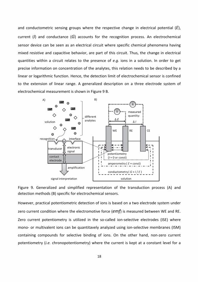
18
and conductometric sensing groups where the respective change in electrical potential (E),
current (I) and conductance (G) accounts for the recognition process. An electrochemical
sensor device can be seen as an electrical circuit where specific chemical phenomena having
mixed resistive and capacitive behavior, are part of this circuit. Thus, the change in electrical
quantities within a circuit relates to the presence of e.g. ions in a solution. In order to get
precise information on concentration of the analytes, this relation needs to be described by a
linear or logarithmic function. Hence, the detection limit of electrochemical sensor is confined
to the extension of linear range. A generalized description on a three electrode system of
electrochemical measurement is shown in Figure 9 B.
Figure 9. Generalized and simplified representation of the transduction process (A) and
detection methods (B) specific for electrochemical sensors.
However, practical potentiometric detection of ions is based on a two electrode system under
zero current condition where the electromotive force (emf) is measured between WE and RE.
Zero current potentiometry is utilized in the so‐called ion‐selective electrodes (ISE) where
mono‐ or multivalent ions can be quantitavely analyzed using ion‐selective membranes (ISM)
containing compounds for selective binding of ions. On the other hand, non‐zero current
potentiometry (i.e. chronopotentiometry) where the current is kept at a constant level for a

19
certain time polarizing the WE (e.g. ISE) is performed within a three electrode system. For
amperometric detection the potential is constant within measurement time and an overall
output signal is determined (ideally) by mass‐transport resistance attributed to analyzed
sample. Conductometric sensors, also referred to as chemiresistors are usually used for
recognition of gases or biological species. In this group of sensors the analytical information is
obtained due to the change in resistivity of a selective material. All electrochemical sensing
groups listed in Figure 9 B can greatly benefit from the use of conducting polymers as a
transducer layer, mostly due to the possibility to enhance the rate of redox processes,
relatively easy immobilization of selective molecules, flexibility in sensor design and
biocompatibility. Importantly, by using conducting polymers in the sensor structure various
electrochemical sensors can be miniaturized and fabricated at low cost. Subjectively the most
notable enhancement of the recognition process with the use of conducting polymers was
carried out within amperometric biosensors and ISEs.
In the ampreometric sensors, the measured current is proportional to the concentration of the
analyte and therefore the systems used in recognition should be easy to be oxidized and
reduced. Owing to the fact that products of enzymatic reactions e.g. O2 or H2O2 can be
accurately detected [62,63], amperometric sensors have extensively been used as biosensors.
The first application of conducting polymer for entrapping an enzyme emerged already in
1980s [64]. In this approach, PPy was electrosynthesized in the presence of glucose oxidase
showing the feasibility of manufacturing robust amperometric glucose sensors. Since then,
several enzymes have been immobilized for detection of many important biologically active
compounds, mostly in e.g. PPy [65‐67], its methyl derivative [68], PANI [69,70] and PEDOT [71].
Also, macromolecules like deoxyribonucleic acid (DNA) can be aperometrically detected on PPy
films modified with immobilized or absorbed oligonucleotide fragments [72‐74]. Amperometric
detection of DNA assisted with conducting polymers appealed an extensive attention, together
with immobilization of antibodies into conducting polymer matrix to create immunoassays.
The latter, resulted in immunosensors that can be fabricated at low cost and also importantly
with direct detection of the target species [75,76].
20
In ISEs, conducting polymers are mainly used as ion‐to‐electron transducers. This approach
enables the possibility of miniaturization of the device and also greatly simplified the
manufacturing process in comparison to classical ISEs where an inner reference solution is
always needed. The so called all‐solid‐state ISE typically consists of either an
electropolymerized or solution casted conducting polymer layer with an ISM deposited on top.
In such a design the overall enhanced ion recognition (especially toward lowering of detection
limit) is attributed to synergy of the interfacial redox properties of the conducting polymers
[77] and the high selectivity of ISM [78]. There are numerous examples of conducting polymers
used as transducer layer in solid‐state ISEs for the detection of ions that are important for
medical or environmental analysis [79]. For instance selective detection of K+ was realized by
using PPy, PEDOT or PANI [80‐82] and nanomolar detection of Pb2+ was accomplished by
utilizing PPy [77]. The other promising approach for selective potentiometric detection of ions
is in a direct use of conducting polymer both as the transducer and the selective layer. This
concept might provide miniaturization of ISEs to nearly a nanodomain and possibility for
immobilizing biomolecules within a single‐layer. Conducting polymer single‐layer ISEs were
already extensively studied for detection of cations or anions (e.g. pH, Ca2+, Cl‐). However, they
are still limited in their overall performance in comparison to sensors with ISMs [79]. Another
highly important application of conducting polymers in zero‐current potentiometry is
fabrication of liquid‐junction free RE. In order to practically realize integrated chemical sensor
the RE needs to also be miniaturized. Notable examples in development of liquid‐junction free
REs are utilization of conducting polymers doped with pH buffering ligands [83] and a
systematic study on surfactant doped PEDOT and PPy covered with poly(vinyl chloride) (PVC)
based membranes [84].
4. New monomers and electrolytes for electrochemical synthesis of electroactive materials
4.1. Polycyclic aromatic hydrocarbons
Fused aromatic molecules have attracted attention as building blocks of polymer backbone
mostly due to the possibility of synthetizing new fluorescent materials. E.g. compounds such as
antracene and pyrene were used as monomers to make conjugated polymers or copolymers

21
[85,86]. Those molecules belong to a wide group of compounds termed polycyclic aromatic
hydrocarbons (PAHs) which are polycyclic organic molecules consisting only of fused rings and
exhibiting a high degree of aromaticity [87]. There is a huge variety of PAHs in both sizes and
symmetries, ranging from naphthalene (bicyclic aromatic hydrocarbon) to macromolecules
consisting of more than two hundred fused rings [88]. Since PAHs in different arrangements
are formed during incomplete combustion of organic compounds they are widely spread
through the terrestrial environment [89]. Owing to the usually planar, aromatic and plain
structure of PAHs, those molecules have a relatively high π‐electron overlap and characteristic
optical spectra. Selected PAHs of environmental, astrophysical and materials science interest
are listed in Figure 10 A. The reason for the numerous publications concerning PAHs are mainly
related to the cancerogenicity of relatively small PAHs (especially BaP) [90] and the formal
similarity of larger PAH molecules to both graphene and disordered graphite [91]. Interestingly,
vibrational motions of PAHs in different sizes and symmetries are being attributed to
characteristic undefined vibrations in the emission spectra of interstellar medium [92].
Figure 10. Chemical structures of PAHs selected as an example (A) together with a schematic
representation of π‐stacking of PAHs molecules and formation of particulate matter made of
randomly distributed PAH clusters (B).

22
As already mentioned, some of the PAHs have been used to synthesize conducting polymers.
Vast majority of the methods to synthetize PAHs‐based copolymers, linear chains or
functionalized conducting polymers rely on chemical synthesis [85,86,93]. However, also
electrochemical synthesis can be successfully used in fabrication of polypyrene and its
copolymers [94]. Another concept in application of PAHs molecules in organic electronics is in
the alignment‐controlled deposition of planar PAHs. In nature, owing to the interactions of
delocalized π‐electrons between planar molecules, PAHs tend to form molecular clusters as
shown in Figure 10 B. With the growth of a cluster the overall energy of the PAH based
molecular system is minimized and this extension is limited to certain length governed by
particular physical conditions. Therefore, PAH clusters aggregate to form amorphous particles
which can be found e.g. in particulate matter resulting from incomplete combustion of
hydrocarbons [95]. In order to take advantage of spontaneous formation of PAH clusters,
numerous publications are devoted to functionalize PAH molecules with aliphatic chains in
order to make them solution processable [88]. Derivitized PAHs self‐assemble to form so‐called
discotic liquid crystals which are highly ordered structures with anisotropic properties [88,96].
On the other hand, non‐ordered PAH aggregates could also be beneficial e.g. in electroactive
templates for sensor or in electrocatalytic applications. The major benefits of synthesizing such
template materials resides on enhanced ion‐to‐electron transduction in comparison to
conducting polymers and affinity of PAHs to carbon‐based substrate electrodes minimizing
charge‐transfer resistance at the WE/conducting layer interface.
4.2. Room temperature ionic liquids
In order to enable any investigations of chemical phenomena and processes taking place at
electrified interfaces, the medium in which ions or compounds of interest are dissolved need
to exhibit sufficient ionic conductivity. This is practically realized through salt, acid or base
additives (i.e. electrolytes) which are selected for particular applications. For electrochemical
synthesis and doping studies of conducting polymers in non‐aqueous media the most common
electrolyte is salt solution. There is also a substantially different class of electrolytes that act
both as solvents and ionic conductors at the same time. These potentially useful media are in
23
principle salts in molten state and are usually referred to as ionic liquids. Since the liquid range
of salts obviously depends on their melting points and thermodynamic stability, it was
practically adopted that an ionic liquid is a salt that melts below ~100 °C. This nomenclature
distinction is arbitrary, and therefore in this work any molten salt which is in liquid state at ~25
°C is referred to as room temperature ionic liquid (RTIL).
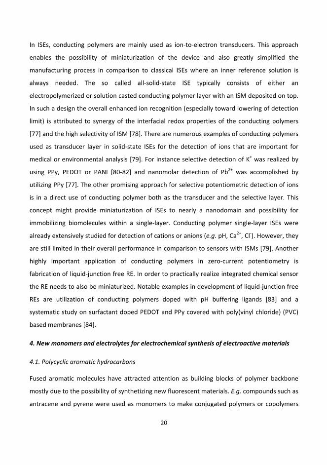
Figure 11. Chemical structures of some most common cations (A) and anions (B) constituting
RTILs. Note: numbered side groups (Rn) refer to different alkyl substitutes and Tf2N− stands for
bis(trifluoromethylsulfonyl) imide.
The reason that RTILs remain liquid at ambient temperatures is attributed to a significant
difference in size between anions and cations with relatively low symmetry which prevents
packing of the lattice [97], as well as charge dissipation [98] and steric hindrance effects [99].
Therefore, representative RTILs consist of bulky organic cations and inorganic anions some of
them illustrated in Figures 11 A and B. From the applied electrochemistry point of view RTILs
exhibit potentially useful properties such as: relatively high ionic conductivity and viscosity,
almost negligible vapor pressure, and a wide electrochemical window (i.e. redox‐free potential
range) [100,101]. Thus, RTILs have been used as media for electropolymerization and doping
studies of conducting polymers greatly enhancing in some cases the deposition process and

24
electrochemical activity of the resultant films in comparison of what can be achieved with
conventional electrolytes. Additionally, since organic solvents are highly volatile and toxic,
RTILs can be considered as powerful alternative electrolytes. On the other hand the commonly
accepted claim that RTILs are non‐toxic solvents is not always valid [102]. Special concern need
to be emphasized on the moisture‐sensitivity of RTILs, since the products of uncontrollable
reactions of e.g. chloroaluminate anions or PF6− with water, can lead to the formation of highly
corrosive acidic environments [103,104]. Also, even for the hydrophobic and moisture‐stable
RTILs, the water content for some particular applications needs to be precisely controlled, due
to a drastic decrease in the available electrochemical window with increasing amount of water
[105].
Moisture‐stable RTILs have successfully been used as electrolytes for electrochemical
polymerization of e.g. PANI [106], PEDOT [107,108], PPy [109,110] and PTs [111]. The observed
pronounced enhancement in quality (e.g. decreased surface roughness), electrochemical
activity or thickness of the resultant conducting polymer films can be attributed to particular
properties of the studied RTILs. Since polymer growth is dependent on concentration of the
reaction products in the vicinity of the electrode, relatively high viscosities of RTILs facilitates
limited transport of those products away from the solution/electrode interface [109]. Also, the
amount of incorporated ions during electrosynthesis is higher in RTILs in comparison to
conventional electrolytes based on molecular solvents [110], which hypothetically results in
both enhanced electrochemical activity and quality of polymer films. Moreover, due to the
extended electrochemical window of RTILs, it is possible to dope conducting polymers at
extreme potential levels. Application of RTILs in electrochemical synthesis of conducting
polymers could be beneficial in fabrication of e.g. amperometric or potentiometric sensors
with considerably higher electrical conductivities facilitating enhanced transduction.

25
5. Synthesis, characterization and deposition techniques of studied electroactive films
5.1. Cyclic voltammetry
In this work cyclic voltammetry (CV) was extensively used as a major technique for
electrochemical synthesis and doping studies of conducting polymers and other electroactive
materials. This potentiodynamic method was also combined with vibrational spectroscopy and
chemiresistive studies to provide additional information about changes in electronic structure
and conductance during redox reactions. In CV the voltage is swept at fixed rate between two
values, one below (E1) and one above (E2) the formal redox potential (E°’) of the analyte.
Hence, within one linear potential scan from E1 to E2, oxidation of the analyte occurs. The
oxidized form of the analyte is reduced back to its original form during the reverse scan.
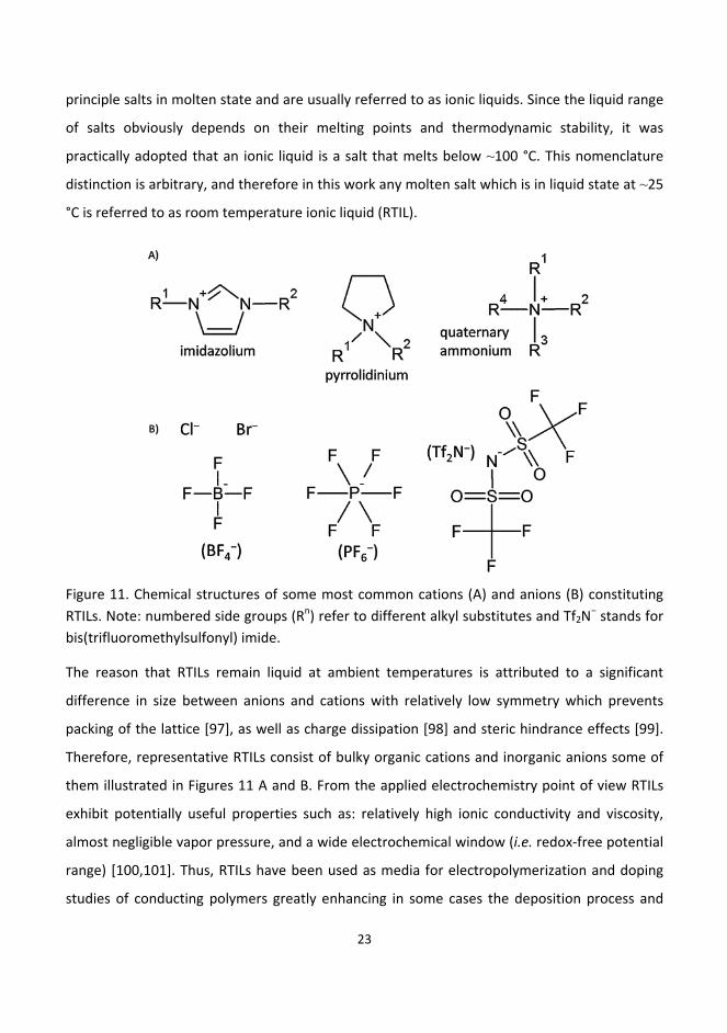
Figure 12. Idealized cyclic voltamograms for a reversible reduction of a hypothetical redox
couple attached to the electrode surface (A) and a system corresponding to a pure capacitor
without any redox reactions present (B). Note: arrows represent “direction” of polarization of
the WE.
Redox reactions are normally studied in a three electrode system as already schematically
shown in Figure 9 B. For practical assay work, the recorded current during potential cycling is
plotted against the applied voltage resulting in the so‐called cyclic voltammogram. A highly
26
idealized current‐voltage curve of a hypothetical redox couple reversibly reduced at a
macroelectrode surface is shown in Figure 12 A. Shape of the cyclic voltammogram is
dependent on the potential scan rate, electrode geometry, concentration of the
oxidized/reduced species and number of electrons involved in the process. Additionally, for
real systems, the diffusion coefficient of electroactive species strongly influences the shape of
the cyclic voltammograms. At macroscale the change in concentration with time is non‐zero,
thus steady‐state current conditions are not reached, leading to the formation of characteristic
peaks in the cyclic voltammogram. The height of those peaks can be described by the Randles‐
Sevcik equation:
k n / / / (3)
Where: Ip is the peak current in A, ks = 269000, ne is the number of transferred electrons, A is
the surface area of the WE in cm2, D is diffusion coefficient in cm2 s−1, v is scan rate in V s−1 and
cb is the bulk concentration of the electroactive species in mol cm−3. Note: equation 3 is valid
assuming that the system is near room temperature. What is practically important in equation
3 is the direct proportionality of the peak current (Ip) to both c and v1/2. Therefore, CV can be
used for detection/monitoring of electroactive species and simultaneously study kinetics of the
reaction. Moreover, the number, shape, presence or absence and position of some particular
peaks in the cyclic voltammogram can give useful information about e.g.
reversibility/irreversibility, oxidation states, reaction mechanism, adsorption or deposition
process. Additionally, the surface area under any current‐voltage curve is in principle the
charge (Q) which passed during the electrochemical process. Therefore, the capacitance (C =
Q / V) involved in those processes can apparently be calculated. Figure 12 B presents the cyclic
voltammogram of an ideal capacitor implying the “plateau current” which is directly
proportional to the scan rate. Conducting polymers with dominant capacitive behavior yield
cyclic voltammograms with rather similar features. In real CV studies of e.g. conducting
polymers, the resulting current‐voltage curves are a combination of several redox reactions,
capacitance of the polymer film and WE as well as a bulk physicochemical properties of
27
electrolyte. Therefore, in order to assign the obtained energy dispersion to a specific system,
knowledge about the background or interfering currents is needed. In conclusions, CV can
relatively easily be implemented in analytical methodology providing practically useful
electrochemical information.
5.2. Molecular spectroscopy
Electronic and molecular structures of different materials characterized in this work were
investigated using both in situ attenuated total reflectance‐Fourier transform infrared (ATR‐
FTIR) and ultraviolet‐visible light (UV‐vis) spectroscopies. Information about molecular
structures was obtained by Raman spectroscopy. The ATR‐FTIR spectra were recorded
simultaneously with CV and for in situ UV‐vis spectroscopy different constant potentials were
applied.
In optical spectroscopy, analytical information is obtained from the changes in the intensity of
the transmitted light during a frequency scan over different excitation wavelengths (Figure 13
A). The IR spectra considered in this work ranges from ~1250 to 16000 nm covering the so‐
called infrared active vibrations (IRAV) specific for each chemical compound and the electronic
absorption region which rises upon the applied electric field to a semiconductor. Within the
UV‐vis part of the electromagnetic spectrum the fundamental transition denoted as either
π*←π or S1←S0 (vide Figure 3 A and Figure 6 A, respectively) occurs. Since in IR spectroscopy
the absorbed energy is considerably lower than in UV‐vis, the molecular vibrations give rise to
the observed vibrational modes corresponding to stretching and bending modes of the studied
molecules. The energy of those modes can sufficiently be described with harmonic oscillator
approximation shown in equation 2. What is practically measured in IR spectroscopy is the
change in molecular dipole moment during the vibration. Figure 13 B shows the principles of
any spectrometer. Macroscopically the intensity of photons interacting with molecules
decreases exponentially according to Lambert‐Beer law. The attenuation coefficient (γf) is
specific for each type of material and the used excitation wavelength. Hence, both FTIR and
28
UV‐vis spectroscopies can be used for quantitative analysis within the linear dependence
between absorption and concentration of the analyte.
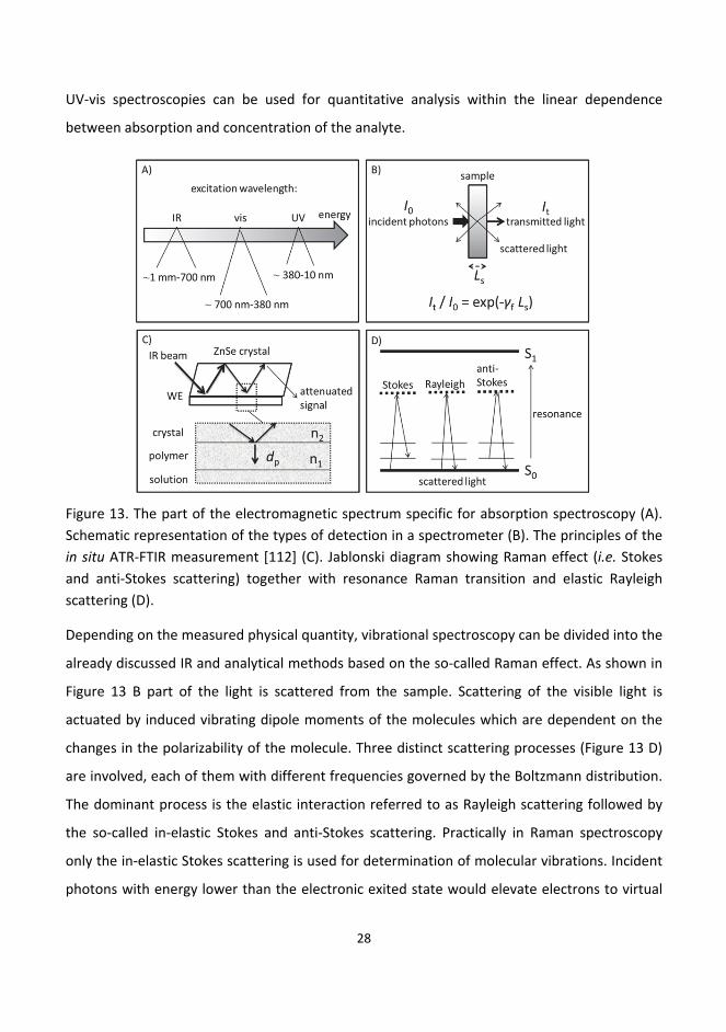
Figure 13. The part of the electromagnetic spectrum specific for absorption spectroscopy (A).
Schematic representation of the types of detection in a spectrometer (B). The principles of the
in situ ATR‐FTIR measurement [112] (C). Jablonski diagram showing Raman effect (i.e. Stokes
and anti‐Stokes scattering) together with resonance Raman transition and elastic Rayleigh
scattering (D).
Depending on the measured physical quantity, vibrational spectroscopy can be divided into the
already discussed IR and analytical methods based on the so‐called Raman effect. As shown in
Figure 13 B part of the light is scattered from the sample. Scattering of the visible light is
actuated by induced vibrating dipole moments of the molecules which are dependent on the
changes in the polarizability of the molecule. Three distinct scattering processes (Figure 13 D)
are involved, each of them with different frequencies governed by the Boltzmann distribution.
The dominant process is the elastic interaction referred to as Rayleigh scattering followed by
the so‐called in‐elastic Stokes and anti‐Stokes scattering. Practically in Raman spectroscopy
only the in‐elastic Stokes scattering is used for determination of molecular vibrations. Incident
photons with energy lower than the electronic exited state would elevate electrons to virtual
29
levels and then the system is relaxed to specific vibrational levels in the electronic ground
state. Therefore, IR and Raman are complementary methods, each providing essentially the
same information about vibrational levels, and depending on changes in dipole moment or
polarizability of the vibrating molecules, the vibrations are only IR or Raman active or both.
In modern spectrometers IR spectral data are collected over a wide frequency range using
Michelson interferometer. The resultant interferogram (i.e. the function of relative intensity
and the position of beam‐splitting mirrors) is mathematically transformed into the IR spectrum
by fast Fourier function. FTIR spectra can be also recorded when the IR beam passes through
e.g. a ZeSe, Ge or diamond crystal specifically fabricated to obtain total internal reflection.
Total reflection is obtained when propagating light encounters a medium with different
refractive index (relation of the light velocities in vacuum and the optical medium) at a certain
angle. In principle, the reflected wave is attenuated due to the evanescent effect. Always,
some fraction of light penetrates the boundary between the crystal and the other optical
medium. For the system presented in Figure 13 C, the penetration depth (dp) depends on the
wavelength of the used radiation, the ratio between the two refractive indexes (n2/n1) and the
angle of incidence. Since the value of dp can be even in the micrometer range, ATR is a
powerful tool in studying the optical properties of thin polymer films.
In a typical in situ ATR‐FTIR measurement, a thin layer of platinum is sputtered on one side of
the ZeSe crystal [112]. Hence, a WE is created on which the conducting polymer can either be
grown or drop‐casted. The whole crystal can be assembled into a three‐electrode system cell.
Therefore, this “combined” technique can be used to study changes in the IR spectrum which
are induced by increasing the magnitude of the electric field. Upon doping of semiconductors
the created charge carriers and their concentration have an influence on the symmetry of the
molecule, and also on the number of vibrational transitions. Thus, the relative intensity of the
IRAV bands is increased and their position in the spectrum could change drastically. Moreover,
since polarons and bipolarons are quasi‐particles consisting of moving electrons or holes with
surrounding deformation, the electrochemical doping induces rise of the electronic transitions
associated with absorption as shown in Figure 6 A. The electronic absorption region is
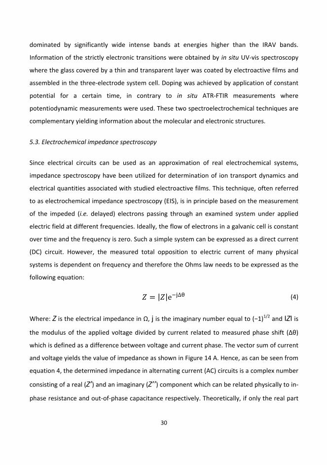
30
dominated by significantly wide intense bands at energies higher than the IRAV bands.
Information of the strictly electronic transitions were obtained by in situ UV‐vis spectroscopy
where the glass covered by a thin and transparent layer was coated by electroactive films and
assembled in the three‐electrode system cell. Doping was achieved by application of constant
potential for a certain time, in contrary to in situ ATR‐FTIR measurements where
potentiodynamic measurements were used. These two spectroelectrochemical techniques are
complementary yielding information about the molecular and electronic structures.
5.3. Electrochemical impedance spectroscopy
Since electrical circuits can be used as an approximation of real electrochemical systems,
impedance spectroscopy have been utilized for determination of ion transport dynamics and
electrical quantities associated with studied electroactive films. This technique, often referred
to as electrochemical impedance spectroscopy (EIS), is in principle based on the measurement
of the impeded (i.e. delayed) electrons passing through an examined system under applied
electric field at different frequencies. Ideally, the flow of electrons in a galvanic cell is constant
over time and the frequency is zero. Such a simple system can be expressed as a direct current
(DC) circuit. However, the measured total opposition to electric current of many physical
systems is dependent on frequency and therefore the Ohms law needs to be expressed as the
following equation:
| |e ∆ (4)
Where: Z is the electrical impedance in Ω, j is the imaginary number equal to (−1)1/2 and IZI is
the modulus of the applied voltage divided by current related to measured phase shift (∆θ)
which is defined as a difference between voltage and current phase. The vector sum of current
and voltage yields the value of impedance as shown in Figure 14 A. Hence, as can be seen from
equation 4, the determined impedance in alternating current (AC) circuits is a complex number
consisting of a real (Z’) and an imaginary (Z’’) component which can be related physically to in‐
phase resistance and out‐of‐phase capacitance respectively. Theoretically, if only the real part
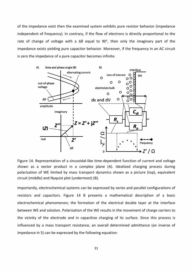
31
of the impedance exist then the examined system exhibits pure resistor behavior (impedance
independent of frequency). In contrary, if the flow of electrons is directly proportional to the
rate of change of voltage with a ∆θ equal to 90°, then only the imaginary part of the
impedance exists yielding pure capacitor behavior. Moreover, if the frequency in an AC circuit
is zero the impedance of a pure capacitor becomes infinite.
Figure 14. Representation of a sinusoidal‐like time‐dependent function of current and voltage
shown as a vector product in a complex plane (A). Idealized charging process during
polarization of WE limited by mass transport dynamics shown as a picture (top), equivalent
circuit (middle) and Nyquist plot (undermost) (B).
Importantly, electrochemical systems can be expressed by series and parallel configurations of
resistors and capacitors. Figure 14 B presents a mathematical description of a basic
electrochemical phenomenon; the formation of the electrical double layer at the interface
between WE and solution. Polarization of the WE results in the movement of charge carriers to
the vicinity of the electrode and in capacitive charging of its surface. Since this process is
influenced by a mass transport resistance, an overall determined admittance (an inverse of
impedance in S) can be expressed by the following equation:
32
ω1 1
1 jω (5)
Where: Rs and Rp are the solution and polarization resistance in Ω, respectively. The
parameter ω is an angular frequency in rad s−1 and Cdl is the double layer capacitance in F. The
value of Rs manifests in a complex impedance plane (also called Nyquist plot) as a shift of the
“first” highest frequency from zero Ω and the value of Rp as a total diameter of the semicircle
in the real part of the impedance. Equation 5 can be used as a practical model for many
reactions which involve charge transfer and are not diffusion‐controlled. The time constant of
the parallel RC circuit can be associated with the kinetics of the studied reactions.
The relatively simple and intuitive model presented by equation 5 is useful in analysis of
frequency dispersion graphs, since if the examined system gives only a semicircle in the
Nyquist plot then one can directly draw conclusions about the electrical quantities of interest
without any need of fitting procedures. On the other hand, for many electrochemical systems,
the overall impedance within both frequency and energy (different oxidation/reduction levels)
dispersion needs to be described by a non‐intuitive model of imperfect capacitor, the so‐called
constant phase element (CPE). This versatile electrical element is nowadays widely used in
equivalent circuit analysis in EIS [113]. CPE can model semi‐infinite linear diffusion (special case
of CPE referred as Warburg impedance) as well as pure resistor and capacitor. When CPE is in
parallel with a resistor it can describe double layer capacitance and charge transfer involved in
the polarization process. The major reason of the great success of CPE in modeling of many
electrochemical systems relies on its ability to provide a robust approximation of porosity. The
Warburg element is implemented in many equivalent circuits to describe diffusion. However,
for thin and porous films it can yield unreasonable results. In such cases, hyperbolic functions
can be applied providing information about finite‐length diffusion. There are two “bounded
Warburg” elements which are based on a cotangent hyperbolic function (referred as O
element) and a tangent hyperbolic one (referred as T element) each describing the impedance
of finite‐length diffusion with a transmissive and reflective boundary, respectively.
33
The detailed analysis of frequency dispersion graphs is typically handled with fitting programs
[113], since many of the elements in equivalent circuits can have very similar mathematical
descriptions or their time constants can be close together. Considering the variety of models
which can have physical meaning and fitting algorithms available, the EIS technique is indeed a
powerful tool in modeling of e.g. electrochemical processes involved in chemical sensing.
Moreover, redox reactions and capacitive charging of conducting polymers or other
electroactive materials can be studied in detail, since impedance can be recorded at any
constant potential of interest, providing information about energy dispersion in the examined
systems.
5.4. Electrical conductivity and in‐situ conductance measurements
Conductivity of the drop‐casted conducting polymer films was determined in this work by
using the four‐point probe measurements. In this technique, the four probes (placed vertically
in line on top of the sample) are equidistant and between the inner ones the voltage is
recorded which corresponds to the applied constant bias current between the outer probes.
Therefore, it is possible to exclude the spreading resistance which becomes significant in low
resistive samples when two‐point probes are used. From the four‐point probe measurement
the bulk resistivity can be estimated according to the following equation:
πln 2
(6)
Where herein: ρ is the resistivity in Ω cm and Lf is the film thickness in cm. If Lf is excluded
from above equation one gets information just about the so‐called “sheet” resistivity.
Depending on the application both resistivity values could be useful (e.g. for relatively very thin
films the approximation of sheet resistivity alone would be sufficient). Equation 6 is valid if Lf is
smaller than half the probe spacing. Typically the conductivity of the samples is calculated
using finite‐size corrections with respect to Lf as well as to the size and shape of the film [114].
34
The four‐point probe technique is practically useful to estimate the bulk or sheet resistivity of
conducting polymers, since those materials are usually deposited as thin films and their
conductivity range is not sufficient for two‐point probe measurements. On the other hand the
major problem in such estimations is establishing an ohmic contact between probes and
sample. At a metal‐semiconductor interface a potential barrier is formed inducing uncertainty
in the measurement. Additional errors may rise due to differences in mechanical properties of
wire probes and polymer surface.
Monitoring the changes in conductance during polymerization and doping reactions were done
in a three electrode system utilizing a WE which was fabricated as a two‐band electrode with a
micrometer range spacing. As in typical conductometric measurements, between band
electrodes with applied constant current, the voltage difference is recorded and related to the
conductance. The growing electroactive film almost immediately covers the gap between the
two bands, thus all the changes in resistance with increasing Lf value can be attributed to
material deposition. This relationship can be described by the following logarithmic function
[115]:
ln8
(7)
Where: Lb and Lsb are the length and half spacing of the double‐band electrodes respectively.
Equation 7 is valid when Lf is greater than Lsb but also smaller than half of the total width of the
double band electrode. In such a case sufficient coverage of the electrode and uniform growth of
electroactive film can be assumed. For such geometrical conditions the current density (J)
related to polymerization can be considered constant. Therefore, when the measured
conductance increases linearly with increasing logarithm of polymerization time, then the
obtained slope of the graph ⁄ equals to the conductivity of the synthesized film.
In situ conductance measurements as presented above can successfully be used in
determination of electrical properties of conducting polymers and other electroactive
materials. Electrical conductivity can be calculated from conductance vs. logarithm of

35
polymerization time plots, for films deposited during both potentiostatic and potentiodynamic
electrosynthesis, with minimal information about films geometry needed. Additionally, this
technique provides insight into changes in the conductance during doping reactions.
5.5. Potentiometric measurements
New materials synthesized or modified to fulfill certain requirements studied in this work were
tested either as a template or solid contact material for ISEs. Fabricated sensors were used in
potentiometric determination of lead which is a significant environmental pollutant. Typical
potentiometric measurements are performed in a two electrode system as schematically
shown in Figure 9 B. When two electrodes are immersed in an electrolyte, after a certain time
equilibrium is reached and the potential of the cell (Ecell) is driven by a spontaneous redox
reaction. If such a circuit is open (practically realized by high input impedance), then the
current flow between WE and RE is minimal and therefore Ecell can be approximated to the
difference of the work (W) conducted in the system divided by the difference in charge (q).
Such an electrochemical system under these conditions is in fact a galvanic cell. Hence, the
relationship between emf and activities of oxidized and reduced ions can be described by the
Nernst equation. In potentiometry, both the formal and redox potential of RE are considered
constant. Therefore, all the changes in emf can be related to the indicator electrode (i.e. WE)
and the half‐cell reaction at the electrolyte/ISM interface (Figure 15 A).
In the case where ISE consist of a conducting substrate and an ISM selective for specific cation,
the Nernst equation can be expressed as:
≅n
ln (8)
Where: Ŕ is ideal gas constant equal to 8.3144621 J mol−1 K−1, F is the Faraday constant equal
to 96485 C mol−1, T is temperature in K. Activities of detected ion in solution and in ISM are
symbolized by ax1 and ax2, respectively (in units of concentration). The practical determination
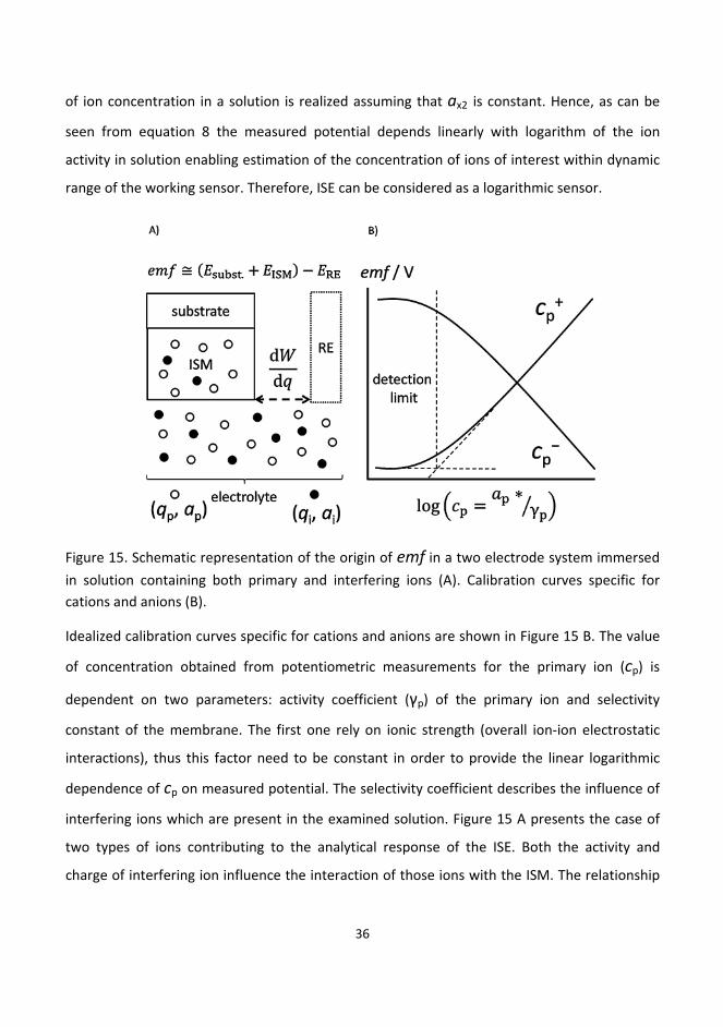
36
of ion concentration in a solution is realized assuming that ax2 is constant. Hence, as can be
seen from equation 8 the measured potential depends linearly with logarithm of the ion
activity in solution enabling estimation of the concentration of ions of interest within dynamic
range of the working sensor. Therefore, ISE can be considered as a logarithmic sensor.
Figure 15. Schematic representation of the origin of emf in a two electrode system immersed
in solution containing both primary and interfering ions (A). Calibration curves specific for
cations and anions (B).
Idealized calibration curves specific for cations and anions are shown in Figure 15 B. The value
of concentration obtained from potentiometric measurements for the primary ion (cp) is
dependent on two parameters: activity coefficient (γp) of the primary ion and selectivity
constant of the membrane. The first one rely on ionic strength (overall ion‐ion electrostatic
interactions), thus this factor need to be constant in order to provide the linear logarithmic
dependence of cp on measured potential. The selectivity coefficient describes the influence of
interfering ions which are present in the examined solution. Figure 15 A presents the case of
two types of ions contributing to the analytical response of the ISE. Both the activity and
charge of interfering ion influence the interaction of those ions with the ISM. The relationship

37
between emf, selectivity coefficient and the activity of primary and interfering ions is given by
the Nikolskij‐Eisenman semi‐empirical equation [116]:
≅ 2.303 log , (9)
Where: LDL is the low detection limit, qp and qi are the charge number of primary and
interfering ions, ap and ai are corresponding activities, and Kp,i symbolize selectivity coefficient
for this particular system. As can be seen from the above equation both Kp,i and ai can
influence the detection limit of the working sensor. However, even if the activity of interfering
ions is close to zero, the plateau region, schematically shown in Figure 15 B, will be still finally
approached (with dilution) due to the reverse flux of primary ions from ISM to the solution.
The major potentiometric characteristics of ISE taken into account during evaluation of the
materials studied here are: LDL, slope of the line obtained during calibration procedure and
hysteresis of the analytical response.
5.6. Surface characterization and deposition at nanoscale
The surfaces of deposited films were characterized by imaging techniques including scanning
electron microscopy (SEM) and atomic force microscopy (AFM). Those techniques provide
imaging with nanometer‐resolution. In electron microscopy an image is produced by analyzing the
interactions of a high energy electron beam with the examined surface. Depending on the actual
need, the analytical signal in SEM can be divided to the so‐called secondary and backscattered
electrons which both can be used for imaging. The images obtained from backscattered electrons
are used for SEM micrographs emphasized on the contrast in composition of the sample.
Additionally, some of the fraction of backscattered electrons are diffracted according to Braggs
law (describing scattering from crystal lattice), yielding X‐radiation (0.01 to 10 nm wavelength).
Hence, a SEM instrument equipped with an energy‐dispersive X‐ray (EDX) analyzer can also give
elemental analysis of the examined SEM image. The secondary electrons are in principle the
generated electrons upon irradiation with energies higher than the ionization potential specific
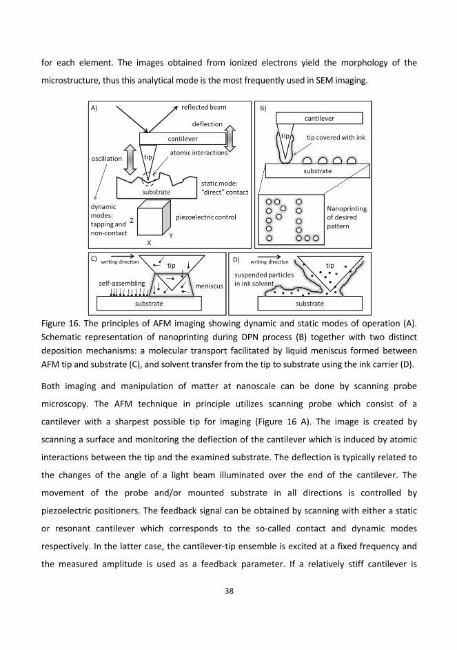
38
for each element. The images obtained from ionized electrons yield the morphology of the
microstructure, thus this analytical mode is the most frequently used in SEM imaging.
Figure 16. The principles of AFM imaging showing dynamic and static modes of operation (A).
Schematic representation of nanoprinting during DPN process (B) together with two distinct
deposition mechanisms: a molecular transport facilitated by liquid meniscus formed between
AFM tip and substrate (C), and solvent transfer from the tip to substrate using the ink carrier (D).
Both imaging and manipulation of matter at nanoscale can be done by scanning probe
microscopy. The AFM technique in principle utilizes scanning probe which consist of a
cantilever with a sharpest possible tip for imaging (Figure 16 A). The image is created by
scanning a surface and monitoring the deflection of the cantilever which is induced by atomic
interactions between the tip and the examined substrate. The deflection is typically related to
the changes of the angle of a light beam illuminated over the end of the cantilever. The
movement of the probe and/or mounted substrate in all directions is controlled by
piezoelectric positioners. The feedback signal can be obtained by scanning with either a static
or resonant cantilever which corresponds to the so‐called contact and dynamic modes
respectively. In the latter case, the cantilever‐tip ensemble is excited at a fixed frequency and
the measured amplitude is used as a feedback parameter. If a relatively stiff cantilever is

39
oscillated close to the sample the tip only intermittently touches the examined surface (the so‐
called tapping mode). In contrary, if the same tip is oscillated further away from the surface
(i.e. non‐contact mode) the majority of the measured forces between the tip and the surface
are the van der Waals type. In the static contact mode cantilevers with a relatively low stiffness
are used and the measuring probe is kept at constant height above the examined surface.
There are several other operational modes currently available for AFM imaging based on the
presented above basic modes, which are adjusted to fulfill certain measurement environments
(e.g. imagining the samples exposed to liquids). With the state‐of‐the‐art AFM instruments it is
possible for some samples even to achieve atomic resolution.
The scanning probe technology can also be used in deposition of various materials at
nanoscale in a form of lines or dots that could be arranged in desired patterns. This can be
done by simply “dipping” the AFM tip into inks containing molecules that are to be deposited
(Figure 16 B). The commercially available technique based on this principle is the so‐called Dip‐
Pen Nanolithography (DPN). Transfer of ink/molecules from the tip to the substrate is limited
mainly by contact time (i.e. dwell) and diffusion rate influenced by physiochemical properties
of the depositing environment. There are two proposed mechanisms of deposition by DPN: the
molecular transfer and physio‐adsorption process (vide Figures 16 C and D, respectively). In the
first one the molecules are delivered to the surface through a liquid meniscus. E.g. DPN‐
controlled deposition of thiols is driven by molecular diffusion yielding self‐assembled
monolayers on gold substrates [117]. It was found that the formation of water meniscus
depends on the surrounding humidity [118]. On the other hand, for dispersions of
nanoparticles, the deposition process is dependent on the nature and energy of the surface,
therefore physio‐adsorption related interactions are dominant [119]. DPN has been already
used for the printing of e.g. proteins, metal nanoparticle and organic compounds [120] as well
as exclusively conducting polymers [121‐123]. Some of the AFM probes produced for DPN
instruments are composed of multi‐cantilever‐tip ensembles. Hence, it is possible to
simultaneously deposit different materials (i.e. multiplexing) at nanoscale with relatively high
accuracy and precision. Additionally, patterning of multiplexed arrays can be extended over
relatively large areas which is desirable e.g. in the fabrication of immunosensors [76].
40
6. Results and discussion
6.1. Electrochemistry of poly(para‐phyenylene) in room temperature ionic liquids
Electrochemical synthesis of conducting polymers assisted with RTILs typically results in
enhanced electroactivity of the deposited films in comparison with classical organic solvents.
Additionally, the material yield electrodeposited in RTILs in some cases, can be significantly
higher. In Paper I, two RTILs representative for pyrrolidinium (R1=methyl, R2=butyl, “bmp”) and
imidazolium (R1=methyl, R2=butyl, “bmim”) cations (vide Figure 11 A) combined with Tf2N− and
PF6− anions respectively, were chosen as model RTILs for polymerization, doping and
spectroelectrochemical studies of PPP. This conducting polymer is interesting for fundamental
studies, since it can be both p‐ and n‐doped to relatively high values. Also, chemical
polymerization conditions of conducting polymers based on benzene can be optimized to
obtain hyperbranched polymers (i.e. dendritic‐like structures) [124]. Since electrochemical
polymerization systems are non‐deterministic with a considerable number of random
variables, the resulting conducting polymers are in rather slightly branched than strictly linear
forms. Application of new electrolytes may be useful in obtaining partial control over the
electrochemical polymerization process to yield either relatively long conjugation length or
branched (i.e. cross‐linked) conducting polymers.
Selected RTILs (bmpTf2N and bmimPF6) were compared with a conventional electrolyte
containing 0.1 M TBAPF6 in acetonitrile (ACN). Electrochemical polymerization of biphenyl was
performed using CV within 0 and 1.8‐1.9 V at 20 mV s−1 scan rate during 10 consecutive cycles.
As can be seen in Figure 17, potential scanning in bmimPF6 resulted in far more complex shape
of CV curves and a higher amount of material deposited compared to bmpTf2N and ACN (0.1 M
TBAPF6). Additionally, it can be suggested that the PPP film made in bmimPF6 has a more rigid
structure, since its redox response does not change significantly in biphenyl‐free electrolyte
during p‐doping (vide CV curve number 4 in Figure 3a in Paper I).
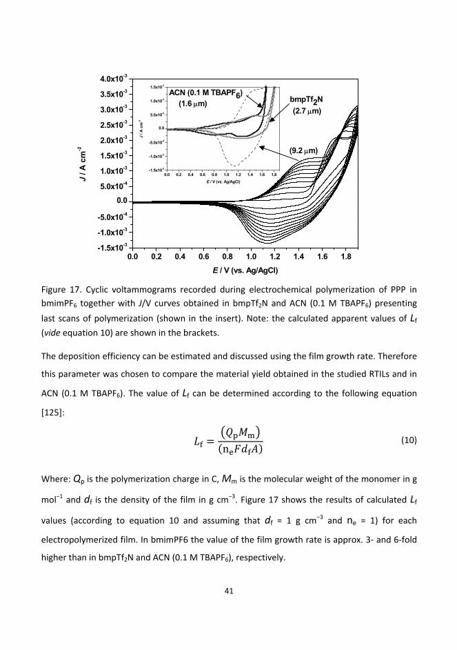
41
Figure 17. Cyclic voltammograms recorded during electrochemical polymerization of PPP in
bmimPF6 together with J/V curves obtained in bmpTf2N and ACN (0.1 M TBAPF6) presenting
last scans of polymerization (shown in the insert). Note: the calculated apparent values of Lf
(vide equation 10) are shown in the brackets.
The deposition efficiency can be estimated and discussed using the film growth rate. Therefore
this parameter was chosen to compare the material yield obtained in the studied RTILs and in
ACN (0.1 M TBAPF6). The value of Lf can be determined according to the following equation
[125]:
n
(10)
Where: Qp is the polymerization charge in C, Mm is the molecular weight of the monomer in g
mol−1 and df is the density of the film in g cm−3. Figure 17 shows the results of calculated Lf
values (according to equation 10 and assuming that df = 1 g cm−3 and ne = 1) for each
electropolymerized film. In bmimPF6 the value of the film growth rate is approx. 3‐ and 6‐fold
higher than in bmpTf2N and ACN (0.1 M TBAPF6), respectively.
0.0 0.2 0.4 0.6 0.8 1.0 1.2 1.4 1.6 1.8-1.5x10⁻³
-1.0x10⁻³
-5.0x10⁻⁴
0.0
5.0x10⁻⁴
1.0x10⁻³
1.5x10⁻³
2.0x10⁻³
2.5x10⁻³
3.0x10⁻³
3.5x10⁻³
4.0x10⁻³
(2.7 m)(1.6 m)
J / A
cm
-2
E / V (vs. Ag/AgCl)
ACN (0.1 M TBAPF6)bmpTf2N
(9.2 m)
0.0 0.2 0.4 0.6 0.8 1.0 1.2 1.4 1.6 1.8-1.5x10⁻³
-1.0x10⁻³
-5.0x10⁻⁴
0.0
5.0x10⁻⁴
1.0x10⁻³
1.5x10⁻³
J /
A c
m-2
E / V (vs. Ag/AgCl)
42
The enhanced deposition rate for this particular ionic liquid over the other examined
electrolytes can be induced by several factors like: viscosity, the stability of intermediate
radicals, monomer concentration, differences in the applied potential (due to electrochemical
windows specific for each electrolyte), solubility of oligomer products as well as the nature of
counterions. Concentration of biphenyl was the same (50 mM) in bmimPF6 and ACN (0.1 M
TBAPF6), thus this factor can be excluded from further considerations. Moreover, the Tf2N−
anion has a negative effect on the polymerization process of PPP, since the optimal
concentration of biphenyl for this RTIL was found to be around 100 mM.
In general, the preferable environment for synthesis of many organic compounds is rather
acidic conditions defined as the presence of a Lewis acid (i.e. electron pair acceptor) [126]. ACN
and Tf2N− can be considered as Lewis bases (i.e. electron pair donor) in contrast to PF6
− or TBA+
ions. Additionally, the differences in the value of E°’ for PPP in the examined electrolytes are
only around 0.1 V and the stability of the intermediate radicals (schematically shown in Figure
8) is unknown. Therefore, a reasonable explanation for the greatly enhance amount of
deposited material in bmimPF6 relies on the significant differences in viscosity (~4‐fold over
bmpTf2N and presumably more than 800‐fold over ACN). Relatively high viscosities of RTILs
“translate” into lower than expected ionic conductivities (also influenced by not fully
dissociated anions and cations [127]) as well as in slower diffusion and mass transport in
comparison to conventional organic electrolytes. On the other hand, for any electrochemical
process the most important is the WE/electrolyte interface. As already discussed in chapter
4.2, the higher concentration of reaction products in the vicinity of the electrode can directly
be related to slower diffusion through RTILs.
The doping process of PPP made in bmimPF6, bmpTf2N and ACN (0.1 M TBAPF6) was examined
during potential dynamic studies in these electrolytes. Additionally, the in situ ATR‐FTIR
spectroscopy enabled more detailed analysis of energy spectra of PPP in comparison to
recorded current/voltage and FTIR spectra alone. It was found that the p‐doping response was
enhanced in bmimPF6 and n‐doping in bmpTf2N, compared to ACN (0.1 M TBAPF6), as can be
seen in Figures 3 and 4 in Paper I. Those results are indicative for relatively higher redox

43
activity of deposited films in RTILs, especially because the CV curves for PPP made and doped
in ACN (0.1 M TBAPF6) suggest a slightly more capacitive response.
Figure 18. Selected in situ ATR‐FTIR spectra of the PPP films made in the electrolytes studied in
Paper I and correlated with the highest applied potential for each particular system. The
difference spectra are within 1650‐650 cm−1 wavenumber region and correspond to p‐doping
in ACN (0.1 M TBAPF6) (A), in bmimPF6 (B) and in bmpTf2N (C), together with n‐doping in
bmpTf2N (D).
Figure 18 shows the FTIR spectra corresponding to IRAV modes at high doping levels. In most
of the studied cases, both the electronic absorption and the intensity of IRAVs raised
significantly during redox reactions of PPP (vide Figures 6 to 10 in Paper I). The typical intense
vibrations observed in the “fingerprint region” for benzene‐based materials are roughly around
1600‐1000 cm−1 which corresponds to C−C and C−H mo ons. For PPP, the Raman ac ve
vibrations in the doped state are at 1595, 1280 and 1220 cm−1, together with IRAV modes at
1530, 1260 and 1180 cm−1 [128]. Since both the Raman and IR spectra of PPP can be discussed
in the terms of effective conjugation coordinate theory (ECC), the frequency dispersion of
some of the observed modes or their intensity relationships can be related to the conjugation
length of polymer materials [128].
*
*
**
*
*
1579
1282
1222
*
*
*
*
1348-11761589
1600 1500 1400 1300 1200 1100 1000 900 800 700
***
**
abso
rban
ce /
a.u.
wavenumber / cm1
ab
sorb
ance
/ a.
u.
wavenumber / cm1
A) B)
C) D)
15801246
1600 1500 1400 1300 1200 1100 1000 900 800 700
**
**
1547
1311
44
For PPP films made in ACN (0.1 M TBAPF6) p‐doping yielded the major IRAV modes at ~1579
and 1222 cm−1 with significantly less intense peak at ~1282 cm−1 (Figure 18 A). The relation in
the intensity of the latter vibration to the peak at ~1222 cm−1 suggests an extended
conjugation length [129]. Although, much more material was deposited during polymerization
of PPP in bmimPF6, the resulting films are probably in a form of slightly branched and rigid
polymer chains. For the films made and p‐doped in bmimPF6 the difference ATR‐FTIR spectrum
(Figure 18 B) exhibit multiple and relatively intensive peaks in the range 1348‐1176 cm−1 and a
broad peak at ~1589 cm−1 indicating a slightly rigid structure and a wide distribution of the
conjugation lengths respectively [130,131]. As can be seen in Figure 18 C and in Figure 3 in
Paper I, the p‐doping response in bmpTf2N is not better than the films made and p‐doped in
ACN (0.1 M TBAPF6), although slightly more material was deposited in this RTIL.
On the other hand, n‐doping of PPP was only effective for films made and doped in bmpTf2N. It
was possible to reduce PPP in bmimPF6. However, the changes upon doping of both the
absorption and IRAV bands were insignificant (vide Figures 9 A and B in Paper I). The ATR‐FTIR
spectrum corresponding to approx. −2 V of applied potential is shown in Figure 18 D. This
spectrum corresponds to the anionic form of PPP and exhibits two major vibrations at ~1547
and 1311 cm−1. In contrary, the p‐doped films correspond to cationic form of polymer. Hence,
the spectral pattern, number of peaks and their position can be slightly different. Additionally,
the doping process depends on the diffusion of ions through the electroactive films. Likewise,
the size and nature of counterions can have either effective or defective impact on both the
polymer structure and microstructure in terms of electrical properties and material stability.
Therefore, a possible explanation of the enhanced electroactivity of PPP made and n‐doped in
bmiTf2N can be related to the more balanced ratio between the molecular weight of cation
and anion in this particular RTIL in contrary to electrolytes containing PF6− anion (e.g. vide
common ions in RTILs presented in Figure 11).
The results presented in Paper I and selectively discussed in this chapter can be used in
fundamental studies of conjugated materials in different directions. Both the electrochemical
synthesis and electroactivity of conducting polymers can be greatly enhanced in RTILs in
45
comparison to conventional electrolytes, which was reflected in the polymerization and doping
studies in the two representative ionic liquids: bmimPF6 and bmiTf2N. Additionally, it was
shown that spectroscopic studies of PPP in RTILs can be useful in revealing new features
related to different structures of conducting polymers. This can be practically useful in
discussion of the theoretical aspect of spectroscopic features of carbon‐based aromatic
electroactive materials.
6.2. Investigation of the water‐soluble conducting polymer BBL derivatives
Charge transport efficiency in semiconducting materials is a key factor in the performance of
electronic devices such as diodes and transistors. In polymer‐based electronic devices, p‐type
semiconductors are mainly used, due to the lack of environmentally stable n‐type conducting
polymers [132]. Additionally, use of n‐type semiconducting polymers in bipolar junctions or to
fabricate ambipolar transistors, results in devices with relatively low field‐effect mobility of
electrons [133] in contrary to e.g. OFETs based on p‐type PTs exhibiting relatively high mobility
of holes [47]. One of the conducting polymers that can provide field‐effect mobility of
electrons at decent levels is the poly(benzimidazobenzophenanthroline) (BBL). Importantly,
this ladder‐type conducting polymer can be reversibly reduced chemically or electrochemically,
yielding relatively high electrical conductivities [134]. For practical realization of all‐plastic
electronic devices there is a need for solution processable materials. However, BBL is insoluble
in common organic solvents. From biosensor technology point of view it is beneficial to
synthesize water soluble conducting polymers. Hence, in Paper II, BBL was functionalized with
poly(ethyleneoxide) PEO side chains to obtain water‐based inks.
Figure 19 presents the four BBL derivatives synthetized for this work, shown here as a function
of the doping charge, together with a hypothetical BBL:PEO structure. The conjugation length
has usually a positive impact on the electoactivity of conducting polymers and the length of
side chains presumably increase the size of insulating regions within the polymer film.
Therefore, the synthesized BBL derivatives had different BBL to PEO ratios, ranging from 1.8 up
to 12 (vide Table 1 in Paper II).
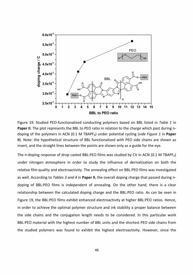
46
Figure 19. Studied PEO‐functionalized conducting polymers based on BBL listed in Table 1 in
Paper II. The plot represents the BBL to PEO ratio in relation to the charge which past during n‐
doping of the polymers in ACN (0.1 M TBAPF6) under potential cycling (vide Figure 1 in Paper
II). Note: the hypothetical structure of BBL functionalized with PEO side chains are shown as
insert, and the straight lines between the points are shown only as a guide for the eye.
The n‐doping response of drop casted BBL:PEO films was studied by CV in ACN (0.1 M TBAPF6)
under nitrogen atmosphere in order to study the influence of derivatization on both the
relative film quality and electroactivity. The annealing effect on BBL:PEO films was investigated
as well. According to Tables 3 and 4 in Paper II, the overall doping charge that passed during n‐
doping of BBL:PEO films is independent of annealing. On the other hand, there is a clear
relationship between the calculated doping charge and the BBL:PEO ratio. As can be seen in
Figure 19, the BBL:PEO films exhibit enhanced electroactivity at higher BBL:PEO ratios. Hence,
in order to achieve the optimal polymer structure and ink stability a proper balance between
the side chains and the conjugation length needs to be considered. In this particular work
BBL:PEO material with the highest number of BBL units and the shortest PEO side chains from
the studied polymers was found to exhibit the highest electroactivity. However, since the
0 1 2 3 4 5 6 7 8 9 10 11 12 13 14 152.5x10⁻³
3.0x10⁻³
3.5x10⁻³
4.0x10⁻³
4.5x10⁻³
5.0x10⁻³
5.5x10⁻³
6.0x10⁻³
do
pin
g c
har
ge
/ C
BBL to PEO ratio
BBL
PEO
n
H
O
OHn
N
N
N
N
OO
O
OH O
OH
O
O
O
O
PEO
PEO
47
properties of BBL:PEO inks have not been studied it is unknown whether this particular
BBL:PEO ratio is the optimal one in practical applications.
As can be seen in Figure 1 in Paper II the BBL derivatives exhibit four clearly resolved redox
processes. The n‐doping response was studied additionally by in situ UV‐vis spectroscopy
(Figures 5 and 7 in Paper II). Both the obtained current/voltage curves and the spectral
patterns are very similar to the conventional BBL [134], indicating a minimal impact of side
chains on the overall n‐doping response. The calculated peak‐to‐peak potential separation (Ep
= Eox – Ered) was found to be independent on the BBL:PEO ratio. The value of Ep was, however,
slightly smaller when BBL:PEO films were annealed (even at relatively low temperatures).
Hence, presumably the size of separation regions created by extension of the side chains
needed to minimized. Also, it was found that annealing had an improving effect on the
morphology of BBL:PEO films as can be seen in the AFM images presented in Figure 4 in Paper
II.
Importantly, BBL:PEO water based inks provided a significant improvement on processability of
the BBL polymers in comparison to conventional BBL which is usually deposited from acidic
solutions. Thus the results presented in Paper II are useful in understanding of the influence of
functionalization of BBL in terms of future development of practical inks based on this
particular ladder‐type conducting polymer. On the other hand, the development of functional
inks based on BBL derivatives needs a thorough study on their physiochemical properties as
well as improvements in the air stability of the deposited films, in order to make a practical use
of the concept presented and summarized in this chapter.

48
6.3. Synthesis, structure and electrochemistry of novel conducting films based on polycyclic
aromatic hydrocarbons
Application of carbon‐based materials that are structurally different from conducting
polymers, with manifold functionality and properties adjusted to specific tasks is an attractive
trend in sensor technology. The nanostructured materials raging from different forms of
carbon nanotubes and fullerenes to graphene, might be beneficial in the future sensor devices.
Nevertheless, the complete integration of the electroactive transduction elements based on
those materials, still represents a challenge, particularly in terms of cost‐to‐performance ratio,
the overall sensor performance and functionality. To date there have been a tremendous
number of scientific reports published on nanostructured carbon based materials connected
also to specific sensor applications. However, very little is known on similar approaches using
PAHs. Those molecules constitute probably the most widely spread organic group of
compounds in the universe. Hence, proper focus on their possible future applications is
definitely needed. The work presented in Papers III and IV is devoted mainly to the application
of benzo(a)pyrene (BaP) as a monomer to obtain relatively larger PAH molecules and
determination of the basic electrical properties of the resulted electroactive films. Since it is
likely that the electrodeposited materials are a mixture of several PAH molecules with different
sizes and symmetries, the name poly(benzopyrene) (PBP) has been adopted.
The structure of BaP is shown in Figure 10 A. Since BaP is one of the most studied PAH
molecules, it was chosen as the model compound in fundamental studies on electrosynthesis
and doping reactions of electroactive films based on PAHs. The first challenge connected with
this research was in finding the optimal conditions for electrochemical synthesis of PBP by CV:
a suitable organic solvent, monomer concentration and scan rate (vide paragraph 3.1 in Paper
III). It was found that the potential cycling from 0 to 1.4 V with 10 mV s−1 and in 20 mM
concentration of BaP dissolved in PC (0.1 M TBAPF6) yields a porous, reproducibly prepared
and electrochemically stable electroactive films. Figure 20 shows a typical J/V curves obtained
during electrosynthesis of PBP together with the recorded changes in the conductance of
growing film. The electrical conductivity of the PBP films estimated by using the first part of
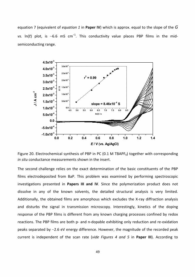
49
equation 7 (equivalent of equation 1 in Paper IV) which is approx. equal to the slope of the G
vs. ln(t) plot, is ~6.6 mS cm−1. This conductivity value places PBP films in the mid‐
semiconducting range.
Figure 20. Electrochemical synthesis of PBP in PC (0.1 M TBAPF6) together with corresponding
in situ conductance measurements shown in the insert.
The second challenge relies on the exact determination of the basic constituents of the PBP
films electrodeposited from BaP. This problem was examined by performing spectroscopic
investigations presented in Papers III and IV. Since the polymerization product does not
dissolve in any of the known solvents, the detailed structural analysis is very limited.
Additionally, the obtained films are amorphous which excludes the X‐ray diffraction analysis
and disturbs the signal in transmission microscopy. Interestingly, kinetics of the doping
response of the PBP films is different from any known charging processes confined by redox
reactions. The PBP films are both p‐ and n‐dopable exhibiting only reduction and re‐oxidation
peaks separated by ~2.6 eV energy difference. However, the magnitude of the recorded peak
current is independent of the scan rate (vide Figures 4 and 5 in Paper III). According to
0.0 0.2 0.4 0.6 0.8 1.0 1.2 1.4-1.0x10⁻³
-5.0x10⁻⁴
0.0
5.0x10⁻⁴
1.0x10⁻³
1.5x10⁻³
2.0x10⁻³
2.5x10⁻³
3.0x10⁻³
3.5x10⁻³
4.0x10⁻³
4.5x10⁻³
4.5 5.0 5.5 6.0 6.5 7.0 7.5 8.0 8.50.0
5.0x10⁻⁴
1.0x10⁻³
1.5x10⁻³
2.0x10⁻³
2.5x10⁻³
3.0x10⁻³
G /
S
ln(t) / s
J / A
cm
-2
E / V (vs. Ag/AgCl)
slope = 8.46x10⁴ S
r2 = 0.99

50
equation 3, the value of Ip is in linear relationship with the square root of the scan rate and to
fulfill this requirement the value of charge which passed during one potential scan need to be
constant over different scan rates. The calculated charge corresponding to p‐ and n‐doping of
PBP at different scan rates is shown at Figure 21. In both cases the doping charge decreases
exponentially with increasing scan rate. Therefore, with increasing scan rate, the amount of
work required to move electrons across the film also need to decrease, indicating the existence
of a highly conducting and ordered network. On the other hand, the value of the PBP “film
resistance” (Rf) (vide measured conductivity) is in contradiction with this suggestion as well as
observed amorphous microstructure.
Figure 21. An example of the charge which passed during doping studies of PBP films (Paper III)
shown as a function of scan rate. Note: the straight lines between presented points are shown
only as a guide for the eye.
The unusual charging behavior of PBP films can be explained by a slow charging process at the
electrolyte/film interface. Hence, this transmissive boundary needs to be dominated by heavily
distributed centers of delocalized π‐electrons originating from relatively large PAH molecules
stacked together in the form of clusters. The absence of long‐range order in PBP films most
0.0 2.0x10⁻² 4.0x10⁻² 6.0x10⁻² 8.0x10⁻²
0.0
2.0x10⁻³
4.0x10⁻³
6.0x10⁻³
8.0x10⁻³
1.0x10⁻²
do
pin
g c
har
ge
/ C
v / V s1
oxidation
reduction

51
probably originates from random arrangement of those molecular clusters as schematically
shown in Figure 10 B. The assumptions about the structure of PBP are verified with the
detailed analysis of both absorption and vibrational spectra of the PBP films. The estimated
optical band gap is ~2.5 eV and the absorption maximum at ~420 nm (vide Figure 6 in Paper
III). Since PAH molecules exhibit characteristic UV‐vis spectra to high extent, those two values
were confronted with the homologous series of PAHs.
Figure 22. The number of π‐electrons in a homologues series of PAH compounds as function of
their optical band gaps according to [135]. The insert shows the crystallite length (La) in the
relation of intensities of vibrations in the center of circumcoronene (Ig) and at the edges (Id)
interpreted as defects in “molecular graphene” [136].
As can be seen in Figure 22, the hypothetical average molecule in the PBP film consists of more
than 50 π‐electrons. The vibrational spectrum recorded in situ at the high oxidation state of
PBP indicates that the average form of the molecule is similar to the cationic form of
circumcoronene (C54H18+). The structure of this compound is presented in Figure 10 A. Owing
to the formal similarity of the PAH compounds to the surface confined graphene, the non‐
resonance Raman spectrum of PBP (Figure 4 in Paper IV) can be compared with the spectral
20 25 30 35 40 45 50 55 60 65 70 75 802.0
2.2
2.4
2.6
2.8
3.0
3.2
3.4
3.6
3.8
4.0
ba
nd
gap
/ e
V
number of electrons
La
La2 = Id / Ig
g
d
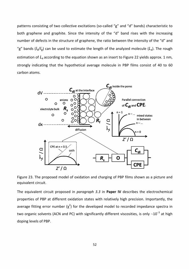
52
patterns consisting of two collective excitations (so‐called “g” and “d” bands) characteristic to
both graphene and graphite. Since the intensity of the “d” band rises with the increasing
number of defects in the structure of graphene, the ratio between the intensity of the “d” and
“g” bands (Id/Ig) can be used to estimate the length of the analyzed molecule (La). The rough
estimation of La according to the equation shown as an insert to Figure 22 yields approx. 1 nm,
strongly indicating that the hypothetical average molecule in PBP films consist of 40 to 60
carbon atoms.
Figure 23. The proposed model of oxidation and charging of PBP films shown as a picture and
equivalent circuit.
The equivalent circuit proposed in paragraph 3.3 in Paper IV describes the electrochemical
properties of PBP at different oxidation states with relatively high precision. Importantly, the
average fitting error number (χ2) for the developed model to recorded impedance spectra in
two organic solvents (ACN and PC) with significantly different viscosities, is only ~10−3 at high
doping levels of PBP.
53
The mathematical description of this new equivalent circuit shown in Figure 23 is the following:
ω1
jω coth jω jω 1 jω (11)
Where: Y0 is the magnitude of admittance in S s1/2 and in S sn for O element and CPE
respectively, B is the time constant related to diffusion in s1/2 and n is the number describing
the discrepancy of CPE from an ideal capacitor (Y0 = C if n = 1 and Y0 = R if n = 0). The parallel
combination of Cdl, at both the interface and inside the pores with CPE, results in a powerful
circuit which can cover the whole range of impedance spectra from a straight line to a
semicircle. The addition of the O element to this circuit is beneficial in description of finite‐
length diffusion through transmissive boundary, especially at high doping levels of the PBP
films. Verification of the model presented by equation 11 was made by direct comparison of
the calculated and measured conductivity values estimated according to equation 7, at the
four highest oxidation states of PBP films (vide Figure 8 in Paper IV). The resultant slopes of the
lines are almost identical for films doped in ACN (0.1 M TBAPF6) strongly indicating that the
model presented above sufficiently predicts the electrical properties of the PBP films.
Therefore, it is an interesting alternative to the frequently used equivalent circuits based on
the Randles model, due to its simplicity and flexibility in the description of “graphically
different” impedance spectra.
The first attempt of the application of PAH‐based electroactive materials in ISEs was presented
in Paper V. BaP was mixed with the anion of the well‐known complexometric indicator
eriochrome black T (EbT) in ACN and relatively thin films were deposited on glassy carbon (GC)
electrodes. EbT− acted both as a dopant for the electrochemically generated PBP film and as a
complexing agent toward lead ions, thus, yielding an ion‐sensitive potentiometric sensor and a
novel template material. The structure of the EbT− anion is shown in the insert in Figure 24.
Divalent cations interact with two oxygen functional groups and two nitrogens present in this
planar molecule. The sulfonyl group in EbT− provides electroneutrality in the PBP films and the
planarity and notable delocalization of π‐electrons around naphthalenic parts presumably
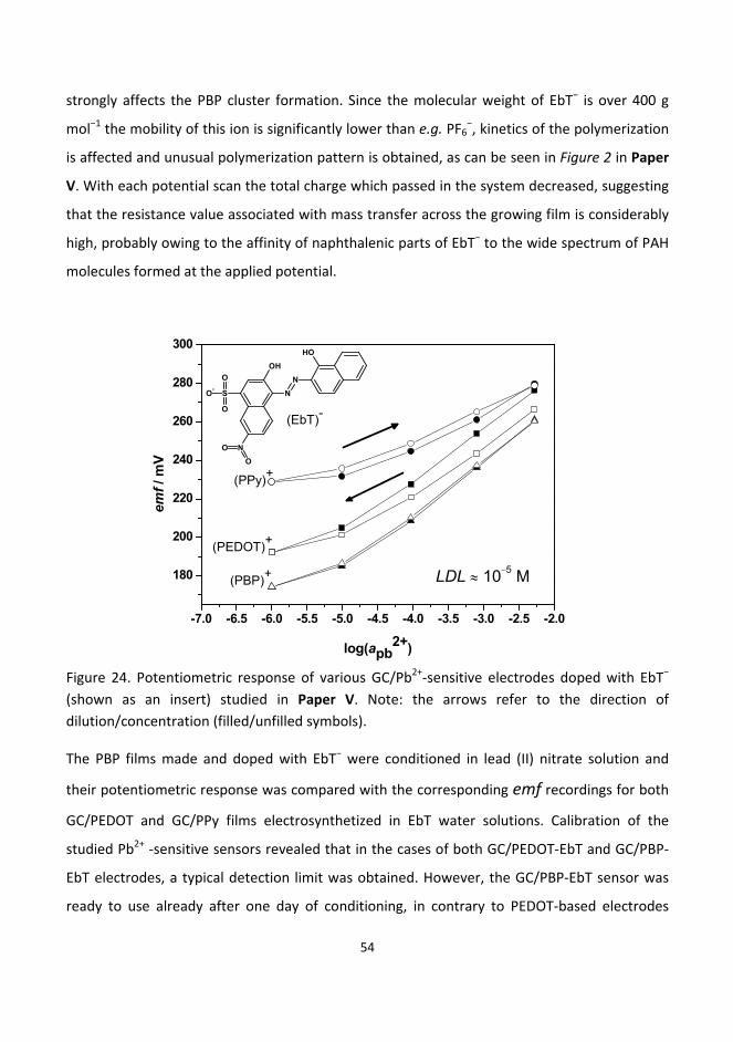
54
strongly affects the PBP cluster formation. Since the molecular weight of EbT− is over 400 g
mol−1 the mobility of this ion is significantly lower than e.g. PF6−, kinetics of the polymerization
is affected and unusual polymerization pattern is obtained, as can be seen in Figure 2 in Paper
V. With each potential scan the total charge which passed in the system decreased, suggesting
that the resistance value associated with mass transfer across the growing film is considerably
high, probably owing to the affinity of naphthalenic parts of EbT− to the wide spectrum of PAH
molecules formed at the applied potential.
Figure 24. Potentiometric response of various GC/Pb2+‐sensitive electrodes doped with EbT−
(shown as an insert) studied in Paper V. Note: the arrows refer to the direction of
dilution/concentration (filled/unfilled symbols).
The PBP films made and doped with EbT− were conditioned in lead (II) nitrate solution and
their potentiometric response was compared with the corresponding emf recordings for both
GC/PEDOT and GC/PPy films electrosynthetized in EbT water solutions. Calibration of the
studied Pb2+ ‐sensitive sensors revealed that in the cases of both GC/PEDOT‐EbT and GC/PBP‐
EbT electrodes, a typical detection limit was obtained. However, the GC/PBP‐EbT sensor was
ready to use already after one day of conditioning, in contrary to PEDOT‐based electrodes
-7.0 -6.5 -6.0 -5.5 -5.0 -4.5 -4.0 -3.5 -3.0 -2.5 -2.0
180
200
220
240
260
280
300
S
O
O
O-
OH
NO
O
N
OH
N
emf
/ mV
log(apb2+)
(EbT)-
LDL 105 M
(PEDOT)+
(PPy)+
(PBP)+
55
which require two days and a constant sub‐Nernstian response of GC/PPy‐EbT electrodes.
Moreover, the hysteresis effect of the Pb2+ ‐sensitive films as shown in Figure 24 of the
GC/PBP‐EbT electrodes is rather small, thus placing these electrodes close to conventional
solid‐state PbS/Ag2S electrode in terms of emf measurement stability. The relatively stable
and fast potentiometric response of the GC/PBP‐EbT electrodes can be attributed to both the
structure and microstructure of PBP‐EbT films as well as a relatively small thickness of the films
obtained in Paper V, in comparison to typical conducting polymers‐based films or PBP made in
PC (0.1 M TBAPF6) that exhibited an extraordinarily high film growth rate.
The presence of lead in PBP doped with EbT after soaking in lead (II) nitrate solution was
confirmed by EDX analysis of the studied films (vide Figure 11 in Paper V). Therefore,
presumably other eriochrome‐type compounds can also be selected for making PAH‐based
templates selective for other divalent cations like Mg2+ or Ca2+ (detection of which is
potentially important in bio‐related applications). Also, since EbT− is a dye which forms a red
chelate with metal ions (in contrary to blue color of free dye), electrodeposited thin layer of
this template material with immobilized EbT, might be useful in optical sensors. PBP‐EbT films
were already successfully used as an ion‐to‐electron transducer in ISEs in lowering of the
detection limit of Pb2+‐ISEs [137].
One‐step electrochemical synthesis of carbon‐based, rigid in structure and porous conducting
templates starting from relatively small PAHs was discussed in this chapter. The novel electrical
model describes accurately the oxidation states of PBP, showing the existence of a
semiconducting amorphous network with physicochemical properties facilitating relatively fast
ion transport. Since presumably different kinds of primary and secondary dopants can be
embodied into herein studied materials, the PAH‐based films can achieve versatile
functionality which could be potentially useful in future chemical sensors or in electrocatalytic
applications.
56
6.4. Development of water‐based PEDOT:PSS inks for nanoprinting and durable chemical sensors
Practical realization of conducting polymer‐based devices depends to a large extent on the
processability of those materials. Industrial or even laboratory scale production demands
materials that can be embodied into manufacturing processes in a reproducible and reliable
way. Since most practical deposition methods are lithography‐related, there is a need for the
development of new inks that would provide sufficient functionality and exhibit suitable
physical properties for printing. Functional design of inks containing electroactive species
mainly concentrates on the tuning of electrical conductivity of printed material despite the
concern about ink properties (e.g. viscosity) for printing purposes. Especially for sensor
applications the deposited conducting polymer films should have relatively low impedances.
The other less explored, however, desirable functionality of conducting polymer‐based inks, is
connected with the long‐term stability of electroactive deposits in certain fluids. The work
presented in Paper VI is devoted to the issues connected with adhesion of PEDOT:PSS films on
electrode substrates in aqueous environments, however, still utilizing water‐based inks for
casting. As already mentioned in paragraph 2.3, conducting PEDOT can be synthesized
together with PSS surfactant yielding material with relatively high solution processability. From
sensor technology point of view this particular conducting polymer is an attractive functional
material mostly due to its relatively low redox potentials combined with sufficient
electrochemical stability [36]. Moreover, PEDOT:PSS exhibit a tolerable level of
biocompatibility [138].
Thin films of PEDOT:PSS can electrochemically be synthesized, thus providing a relatively easy
way of making functional chemical sensors on existing electrode patterns. In such a case the
adhesion of the PEDOT:PSS films to the various conducting substrates in aqueous media is
usually sufficient. On the other hand, the adhesion of solution cast PEDOT:PSS to different
surfaces in water is very limited [139], thus leading to severe restrictions e.g. in bio‐related
applications or ion detection in environmental samples. About half of the sulfonyl groups in
the PSS polyanion are not involved in the doping of PEDOT [140]. Therefore, PEDOT:PSS in
water is in the form of particles consisting of a PEDOT‐rich core and PSS‐rich outer shell.
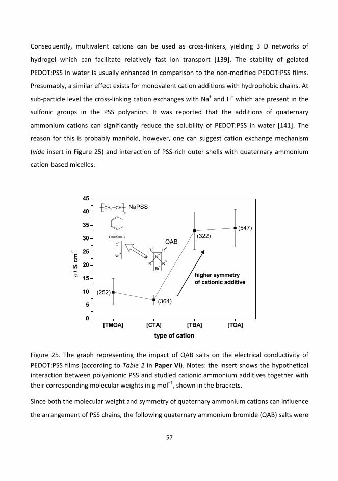
57
Consequently, multivalent cations can be used as cross‐linkers, yielding 3 D networks of
hydrogel which can facilitate relatively fast ion transport [139]. The stability of gelated
PEDOT:PSS in water is usually enhanced in comparison to the non‐modified PEDOT:PSS films.
Presumably, a similar effect exists for monovalent cation additions with hydrophobic chains. At
sub‐particle level the cross‐linking cation exchanges with Na+ and H+ which are present in the
sulfonic groups in the PSS polyanion. It was reported that the additions of quaternary
ammonium cations can significantly reduce the solubility of PEDOT:PSS in water [141]. The
reason for this is probably manifold, however, one can suggest cation exchange mechanism
(vide insert in Figure 25) and interaction of PSS‐rich outer shells with quaternary ammonium
cation‐based micelles.
Figure 25. The graph representing the impact of QAB salts on the electrical conductivity of
PEDOT:PSS films (according to Table 2 in Paper VI). Notes: the insert shows the hypothetical
interaction between polyanionic PSS and studied cationic ammonium additives together with
their corresponding molecular weights in g mol−1, shown in the brackets.
Since both the molecular weight and symmetry of quaternary ammonium cations can influence
the arrangement of PSS chains, the following quaternary ammonium bromide (QAB) salts were
[TMOA] [CTA] [TBA] [TOA]0
5
10
15
20
25
30
35
40
45
/ S
cm
-1
type of cation
higher symmetry of cationic additive
(252)
(364)
(322)(547)
NaPSS
QAB
CH2 CH
S OO
O-
n
Na+
Br-
N+
R1
R2
R4
R3

58
studied in Paper VI: trimetyloctylammonium (R1‐3=methyl, R4=octyl, “TMOA”),
hexadecyltrimethylammonium (R1‐3=methyl , R4=hexadecyl, “CTA”), tetrabutylammonium (R1‐
4=butyl “TBA”) and tetraoctylammonium (R1‐4=octyl “TOA”). Those salts were dissolved in
ethylene glycol (EG) to yield 0.05 M solutions which were used as soaking media of PEDOT:PSS
deposits on GC electrodes. Addition of polyalcohols is known to significantly increase the
electrical conductivity of PEDOT:PSS via a secondary doping mechanism which leads to the
decrease in thickness of the PSS barrier separating the PEDOT‐rich grains [142]. Presumably,
the number of polar groups in polyalcohol can have an effective impact on the overall
conductivity, thus, QAB salts might exhibit a similar feature. Since the selected additives
studied in Paper VI, were also intended to meet requirements regarding printing, the EG was
chosen due to its sufficient thickening properties and the ability to effectively dissolve a wider
range of QAB salts than other more viscous polyalcohols. Also, addition of surfactants in the
form of QABs is highly beneficial. As can be seen in Table 2 in Paper VI and Figure 25, all
studied EG‐QAB modifiers resulted in enhanced conductivity of the PEDOT:PSS films. However,
the cations with higher symmetry were found to be more effective in optimization of PEDOT
chains toward higher conductivities.
A highly important finding regarding the GC/PEDOT:PSS electrodes modified with EG‐QABs is
connected with their outstanding durability in aqueous solutions (also with low pH values). As
can be seen from Figures 1 and 2 in Paper VI, the studied systems survived 60 days of constant
soaking in citrate buffer (pH 4) with minimal decrease in electroactivity. In order to quantify
the transport dynamics of those electrochemical systems, several EIS measurements were
performed. Recorded impedance spectra were fitted to the model composed of a resistor
connected in series with a T element. The mathematical description of this model is presented
below:
1
(12)
Since PEDOT:PSS exhibits capacitor‐like behavior, the impedance spectra (shown as Nyquist
plot) of EG‐QAB‐modified PEDOT:PSS electrodes were dominated by a vertical line (reflective
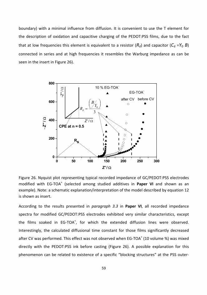
59
boundary) with a minimal influence from diffusion. It is convenient to use the T element for
the description of oxidation and capacitive charging of the PEDOT:PSS films, due to the fact
that at low frequencies this element is equivalent to a resistor (Rd) and capacitor (Cd =Y0 B)
connected in series and at high frequencies it resembles the Warburg impedance as can be
seen in the insert in Figure 26).
Figure 26. Nyquist plot representing typical recorded impedance of GC/PEDOT:PSS electrodes
modified with EG‐TOA+ (selected among studied additives in Paper VI and shown as an
example). Note: a schematic explanation/interpretation of the model described by equation 12
is shown as insert.
According to the results presented in paragraph 3.3 in Paper VI, all recorded impedance
spectra for modified GC/PEDOT:PSS electrodes exhibited very similar characteristics, except
the films soaked in EG‐TOA+, for which the extended diffusion lines were observed.
Interestingly, the calculated diffusional time constant for those films significantly decreased
after CV was performed. This effect was not observed when EG‐TOA+ (10 volume %) was mixed
directly with the PEDOT:PSS ink before casting (Figure 26). A possible explanation for this
phenomenon can be related to existence of a specific “blocking structures” at the PSS outer‐
0 50 100 150 200 250 3000
200
400
600
800
CPE at n = 0.5Z' /
-Z''
/
Z''
/
Z' /
10 % EG-TOA
after CV before CV
EG-TOA
Rs
30
YB
Rd

60
shells facilitated by both relatively long chains and branched TOA+ cations. Those specific
structures might be influenced by ion transport into and out of the film during potential
cycling. The PEDOT:PSS films casted from inks containing 10 volume % of EG‐TOA+ were
annealed before exposure to water and the conductivity of those films were slightly higher
than films modified by soaking. Thus, the following suggestion can be made that the applied
temperature (~100 °C) further decreased the distance between the individual PEDOT:PSS
particles. The calculated apparent diffusion coefficient utilizing the constant B (vide equation
12) and estimated film thickness of ~10 μm, is in the range of 10−6‐10−5 cm2 s−1, indicating that
PEDOT:PSS films modified with EG‐QAB are likely to be in the form of swollen hydrogels which
facilitates ion transfer.
The more practical approach for modification of PEDOT:PSS films other than soaking is the
direct addition of the modifier to the ink. However, it was found that only the addition of TOA+
cation provided enhanced adhesion. Therefore, this QAB salt could be considered in designing
a variety of water‐based PEDOT:PSS inks that could be utilized for e.g. ink‐jet printing.
Nevertheless, all of the studied modified PEDOT:PSS films were tested as a solid‐contact
material in Pb2+‐ISEs (Figure 5 in Paper VI). Only the films modified with EG‐CTA+ and EG‐TOA+
exhibited instant close‐to‐Nerstian response with LDL of ~10−7 M, after 2 days of conditioning
in lead (II) nitrate. Figure 27 presents a comparison between the potentiometric response of
the GC/PEDOT:PSS/PVC‐based Pb2+‐ISE electrodes where the solid‐contact was modified by
soaking in EG‐TOA+ and of conventional solid‐state PbS/Ag2S electrode. The modification of
PEDOT:PSS seems to be beneficial, since both LDL and measurement uncertainty at low
activity of Pb2+ are improved. The insert in Figure 27 shows the corresponding response of an
electrode with the PEODT:PSS solid‐contact that was modified by 10 % volume addition of EG‐
TOA+ to the ink. Similar characteristic in terms of the slope and LDL were obtained after
several measurements and it has to be concluded that the sensor based on 10 % volume
addition of EG‐TOA+ at this stage of the research cannot be used instantaneously after
conditioning. On the other hand, after 10 days potential stability test of the solid‐contact Pb2+‐
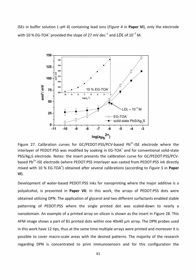
61
ISEs in buffer solution (~pH 4) containing lead ions (Figure 4 in Paper VI), only the electrode
with 10 % EG‐TOA+ provided the slope of 27 mV dec−1 and LDL of 10−7 M.
Figure 27. Calibration curves for GC/PEDOT:PSS/PCV‐based Pb2+‐ISE electrode where the
interlayer of PEDOT:PSS was modified by soaking in EG‐TOA+ and for conventional solid‐state
PbS/Ag2S electrode. Notes: the insert presents the calibration curve for GC/PEDOT:PSS/PCV‐
based Pb2+‐ISE electrode (where PEDOT:PSS interlayer was casted from PEDOT:PSS ink directly
mixed with 10 % EG‐TOA+) obtained after several calibrations (according to Figure 5 in Paper
VI).
Development of water‐based PEDOT:PSS inks for nanoprinting where the major additive is a
polyalcohol, is presented in Paper VII. In this work, the arrays of PEDOT:PSS dots were
obtained utilizing DPN. The application of glycerol and two different surfactants enabled stable
patterning of PEDOT:PSS where the single printed dot was scaled‐down to nearly a
nanodomain. An example of a printed array on silicon is shown as the insert in Figure 28. This
AFM image shows a part of 81 printed dots within one 40x40 μm array. The DPN probes used
in this work have 12 tips, thus at the same time multiple arrays were printed and moreover it is
possible to cover macro‐scale areas with the desired patterns. The majority of the research
regarding DPN is concentrated to print immunosensors and for this configuration the
-11 -10 -9 -8 -7 -6 -5 -4 -30
25
50
75
100
125
150
LDL 106 M
emf
/ mV
log(aPb2+)
EG-TOA
solid-state PbS/Ag2S
-10 -9 -8 -7 -6 -5 -4 -3200
225
250
275
300
325
350
emf
/ mV
log(aPb
2+)
10 % EG-TOA
62
deposition of desired moieties is driven by molecular transport facilitated by water meniscus
formed between the tip and substrate. For the other inks containing extensive amount of
nanoparticles, the mass transfer is governed by processes related to physio‐adsorption. For
those two proposed deposition mechanisms schematically shown in Figures 16 C and D, the
different composition of inks needs to be considered. The deposition of e.g. relatively small
molecules or nanoparticles does not need significant adjustment of ink properties, since the
influence of dispersed moieties on the overall viscosity and ink stability during printing is
minimal. Therefore, nanoprinting of dispersed conducting polymers is challenging, due to the
considerable sizes of conducting particles and their complex interactions with the surrounding
environment.
The selective patterning of PEDOT:PSS arrays via DPN to complement the ink‐jet printing, may
be useful in applications such as, for example, chemical sensors with enhanced signal‐to‐noise
ratio or as hosts for living cells with the possibility to electrically stimulate them. Figures 28 A
and B presents the obtained dot dimensions for the first attempts to deposit PEDOT:PSS with
DPN. The commercial PEDOT:PSS water‐based inks without any modification did not give
reproducible DPN printing. Hence, in one approach the whole set of tips was dipped to the
mixtures of PEDOT:PSS and methanol, yielding gelated structures [123]. In such a case, an
average dot width is at 1‐1.2 μm level, similarly when Mg2+ cations were used as additional
cross‐linker. Depending on conditions that are difficult to control it was possible to scale down
the dot widths to 800 or even to 600 nm. However, since in DPN extremely small volumes of
ink are used, any changes in surrounding environment highly influence both ink and printing
stability. Additionally, these printed nanoarrays do not survive after exposure to water.
Therefore, in order to provide a reproducible patterning from PEDOT:PSS, a more rational ink
design was needed.
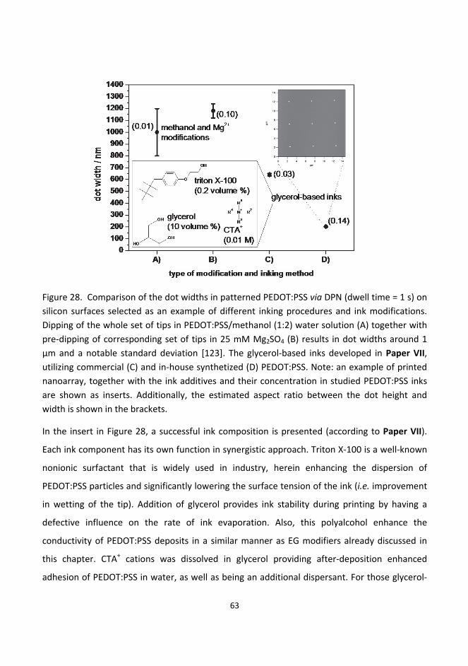
63
Figure 28. Comparison of the dot widths in patterned PEDOT:PSS via DPN (dwell time = 1 s) on
silicon surfaces selected as an example of different inking procedures and ink modifications.
Dipping of the whole set of tips in PEDOT:PSS/methanol (1:2) water solution (A) together with
pre‐dipping of corresponding set of tips in 25 mM Mg2SO4 (B) results in dot widths around 1
μm and a notable standard deviation [123]. The glycerol‐based inks developed in Paper VII,
utilizing commercial (C) and in‐house synthetized (D) PEDOT:PSS. Note: an example of printed
nanoarray, together with the ink additives and their concentration in studied PEDOT:PSS inks
are shown as inserts. Additionally, the estimated aspect ratio between the dot height and
width is shown in the brackets.
In the insert in Figure 28, a successful ink composition is presented (according to Paper VII).
Each ink component has its own function in synergistic approach. Triton X‐100 is a well‐known
nonionic surfactant that is widely used in industry, herein enhancing the dispersion of
PEDOT:PSS particles and significantly lowering the surface tension of the ink (i.e. improvement
in wetting of the tip). Addition of glycerol provides ink stability during printing by having a
defective influence on the rate of ink evaporation. Also, this polyalcohol enhance the
conductivity of PEDOT:PSS deposits in a similar manner as EG modifiers already discussed in
this chapter. CTA+ cations was dissolved in glycerol providing after‐deposition enhanced
adhesion of PEDOT:PSS in water, as well as being an additional dispersant. For those glycerol‐
64
based inks a significant improvement in the scaling‐down of dot dimensions was observed
(vide Figures 28 C and D). With certain dwell times it was possible to print dots with less than
200 nm in diameter as can be observed in Figure 4 in Paper VII. Importantly, the standard
deviation of the dot dimensions indicates the degree of uniformity and reproducibility of the
patterning, which is also similar to that reported during DPN printing of thiols and acid
monolayers deposited on gold [143] for which the deposition is facilitated by the formation of
a water meniscus. This significant improvement was obtained on both silicon and gold
substrates by utilizing in‐house synthetized PEDOT:PSS instead of the commercial material. The
calculated aspect ratios (shown in Figure 28) for in‐house synthetized PEDOT:PSS‐based inks is
~5‐fold larger in comparison to commercial PEDOT:PSS‐based inks discussed in this work. This
indicates that by proper adjustment of the ratio of PEDOT to PSS to be used in chemical
synthesis, notable more material can be delivered at nano‐confined volumes.
This chapter aimed to summarize the research on modification of PEDOT:PSS films with
relatively large cations and polyalcohols. The addition of QAB salts resulted in cross‐linked
PEDOT:PSS particles and in enhanced adhesion and conductivity of the PEDOT:PSS deposited. It
was found that with the use of relatively easy protocols for obtaining PEDOT:PSS water‐based
inks it is possible to obtain durable chemical sensors with sufficient recognition characteristics
as well as arrays of conducting polymers with nanoscale features.

65
7. Final summary and possible future directions
The fundamental studies conducted on π‐conjugated systems, discussed in this work, affirmed
the importance of electrochemistry as a set of “principles and tools” that are useful in
implementation of new ideas in sensor science. Since one can predict that in the near future
organic electronics will be tightly connected with sensor technology, the results presented
above (especially on ink development and PAH‐based structures) might form a solid basis for
further development of new commercial functional devices.
OFETs in integrated circuits and scaled‐down to nanometer range could be the future of
chemical sensing, bioelectronics or in energy storage and conversion applications. This would
be possible by tuning the properties of conducting polymer based‐inks for e.g. ink‐jet printing.
It was shown in Papers VI and VII that by a proper selection of cationic surfactants and
polyalcohols one can obtain the desired synergy of ink additives for a particular printing
process and application. Also, the characterization studies were performed on n‐type
conducting BBL derivatives (Paper II) which are meant for water‐based inks suitable to deposit
active layers in e.g. OFETs. The development of different conducting polymer water‐based inks
is useful in getting closer to printing of biomolecules and implementing them into recognition
processes in bio‐related applications.
The electroactivity of functional layers in chemical sensors based on electrosynthesized
conducting polymers can be elevated by utilization of ionic liquid electrolytes. Some of the
issues connected with this concept, were explored in Paper I. Also, ionic liquids with relatively
high viscosity might be employed for electrochemical synthesis of larger PAH structures,
resulting in even better electroactive templates than presented and characterized in Papers III
and IV. Importantly, the developed electrical model describing different oxidation states of
PBP films can presumably be utilized for other porous electrified templates or networks,
providing sufficient and reliable approximation of reality. In addition to the synthesis and
characterization of electroactive materials, the concepts of utilization of new templates and
modifiers in chemical sensing (particularly for ISEs) have been affirmed in Papers V and VI.
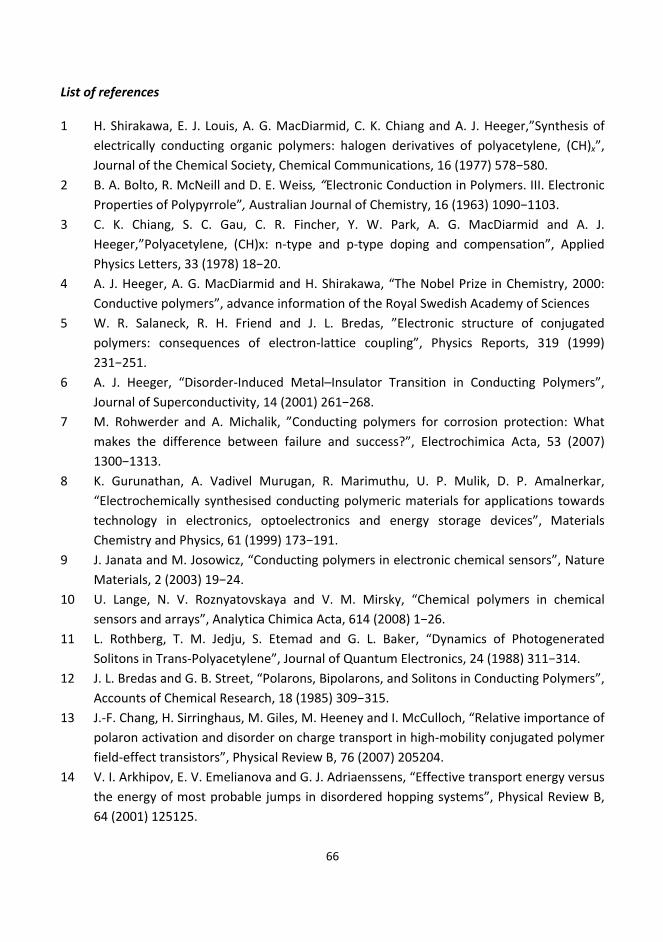
66
List of references
1 H. Shirakawa, E. J. Louis, A. G. MacDiarmid, C. K. Chiang and A. J. Heeger,”Synthesis of
electrically conducting organic polymers: halogen derivatives of polyacetylene, (CH)x”,
Journal of the Chemical Society, Chemical Communications, 16 (1977) 578−580.
2 B. A. Bolto, R. McNeill and D. E. Weiss, “Electronic Conduction in Polymers. III. Electronic
Properties of Polypyrrole”, Australian Journal of Chemistry, 16 (1963) 1090−1103.
3 C. K. Chiang, S. C. Gau, C. R. Fincher, Y. W. Park, A. G. MacDiarmid and A. J.
Heeger,”Polyacetylene, (CH)x: n‐type and p‐type doping and compensation”, Applied
Physics Letters, 33 (1978) 18−20.
4 A. J. Heeger, A. G. MacDiarmid and H. Shirakawa, “The Nobel Prize in Chemistry, 2000:
Conductive polymers”, advance information of the Royal Swedish Academy of Sciences
5 W. R. Salaneck, R. H. Friend and J. L. Bredas, ”Electronic structure of conjugated
polymers: consequences of electron‐lattice coupling”, Physics Reports, 319 (1999)
231−251.
6 A. J. Heeger, “Disorder‐Induced Metal–Insulator Transition in Conducting Polymers”,
Journal of Superconductivity, 14 (2001) 261−268.
7 M. Rohwerder and A. Michalik, ”Conducting polymers for corrosion protection: What
makes the difference between failure and success?”, Electrochimica Acta, 53 (2007)
1300−1313.
8 K. Gurunathan, A. Vadivel Murugan, R. Marimuthu, U. P. Mulik, D. P. Amalnerkar,
“Electrochemically synthesised conducting polymeric materials for applications towards
technology in electronics, optoelectronics and energy storage devices”, Materials
Chemistry and Physics, 61 (1999) 173−191.
9 J. Janata and M. Josowicz, “Conducting polymers in electronic chemical sensors”, Nature
Materials, 2 (2003) 19−24.
10 U. Lange, N. V. Roznyatovskaya and V. M. Mirsky, “Chemical polymers in chemical
sensors and arrays”, Analytica Chimica Acta, 614 (2008) 1−26.
11 L. Rothberg, T. M. Jedju, S. Etemad and G. L. Baker, “Dynamics of Photogenerated
Solitons in Trans‐Polyacetylene”, Journal of Quantum Electronics, 24 (1988) 311−314.
12 J. L. Bredas and G. B. Street, “Polarons, Bipolarons, and Solitons in Conducting Polymers”,
Accounts of Chemical Research, 18 (1985) 309−315.
13 J.‐F. Chang, H. Sirringhaus, M. Giles, M. Heeney and I. McCulloch, “Relative importance of
polaron activation and disorder on charge transport in high‐mobility conjugated polymer
field‐effect transistors”, Physical Review B, 76 (2007) 205204.
14 V. I. Arkhipov, E. V. Emelianova and G. J. Adriaenssens, “Effective transport energy versus
the energy of most probable jumps in disordered hopping systems”, Physical Review B,
64 (2001) 125125.
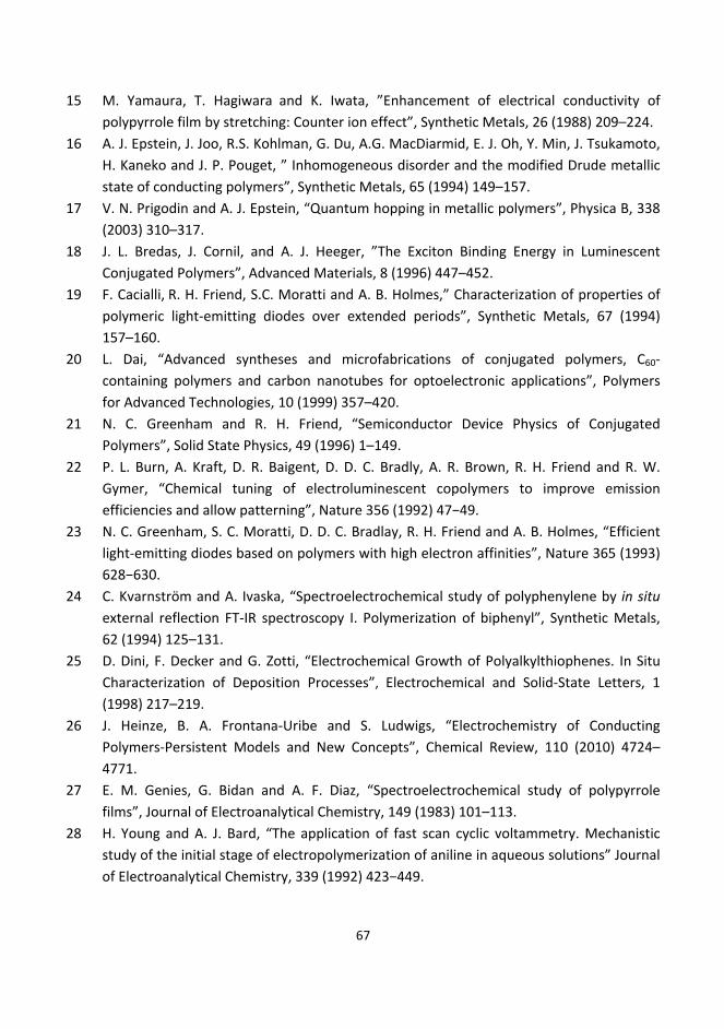
67
15 M. Yamaura, T. Hagiwara and K. Iwata, ”Enhancement of electrical conductivity of
polypyrrole film by stretching: Counter ion effect”, Synthetic Metals, 26 (1988) 209–224.
16 A. J. Epstein, J. Joo, R.S. Kohlman, G. Du, A.G. MacDiarmid, E. J. Oh, Y. Min, J. Tsukamoto,
H. Kaneko and J. P. Pouget, ” Inhomogeneous disorder and the modified Drude metallic
state of conducting polymers”, Synthetic Metals, 65 (1994) 149–157.
17 V. N. Prigodin and A. J. Epstein, “Quantum hopping in metallic polymers”, Physica B, 338
(2003) 310–317.
18 J. L. Bredas, J. Cornil, and A. J. Heeger, ”The Exciton Binding Energy in Luminescent
Conjugated Polymers”, Advanced Materials, 8 (1996) 447–452.
19 F. Cacialli, R. H. Friend, S.C. Moratti and A. B. Holmes,” Characterization of properties of
polymeric light‐emitting diodes over extended periods”, Synthetic Metals, 67 (1994)
157–160.
20 L. Dai, “Advanced syntheses and microfabrications of conjugated polymers, C60‐
containing polymers and carbon nanotubes for optoelectronic applications”, Polymers
for Advanced Technologies, 10 (1999) 357–420.
21 N. C. Greenham and R. H. Friend, “Semiconductor Device Physics of Conjugated
Polymers”, Solid State Physics, 49 (1996) 1–149.
22 P. L. Burn, A. Kraft, D. R. Baigent, D. D. C. Bradly, A. R. Brown, R. H. Friend and R. W.
Gymer, “Chemical tuning of electroluminescent copolymers to improve emission
efficiencies and allow patterning”, Nature 356 (1992) 47−49.
23 N. C. Greenham, S. C. Moratti, D. D. C. Bradlay, R. H. Friend and A. B. Holmes, “Efficient
light‐emitting diodes based on polymers with high electron affinities”, Nature 365 (1993)
628−630.
24 C. Kvarnström and A. Ivaska, “Spectroelectrochemical study of polyphenylene by in situ
external reflection FT‐IR spectroscopy I. Polymerization of biphenyl”, Synthetic Metals,
62 (1994) 125–131.
25 D. Dini, F. Decker and G. Zotti, “Electrochemical Growth of Polyalkylthiophenes. In Situ
Characterization of Deposition Processes”, Electrochemical and Solid‐State Letters, 1
(1998) 217–219.
26 J. Heinze, B. A. Frontana‐Uribe and S. Ludwigs, “Electrochemistry of Conducting
Polymers‐Persistent Models and New Concepts”, Chemical Review, 110 (2010) 4724–
4771.
27 E. M. Genies, G. Bidan and A. F. Diaz, “Spectroelectrochemical study of polypyrrole
films”, Journal of Electroanalytical Chemistry, 149 (1983) 101–113.
28 H. Young and A. J. Bard, “The application of fast scan cyclic voltammetry. Mechanistic
study of the initial stage of electropolymerization of aniline in aqueous solutions” Journal
of Electroanalytical Chemistry, 339 (1992) 423−449.
68
29 G. A. Sotzing, J. R. Reynolds and P. J. Steel, “Poly(3,4‐ethylenedioxythiophene) (PEDOT) prepared via electrochemical polymerization of EDOT, 2,2′‐Bis(3,4‐
ethylenedioxythiophene) (BiEDOT), and their TMS derivatives”, Advanced Materials, 9
(1997) 795–798.
30 F. L. Klavetter and R. H. Grubbs, “Polycyclooctatetraene (polyacetylene): synthesis and
properties”, Journal of the American Chemical Society, 110 (1988) 7807–7813.
31 S. A. Jenekhe and P. O. Johnson, “Complexation‐mediated solubilization and processing
of rigid‐chain and ladder polymers in aprotic organic solvents”, Macromolecules, 23
(1990) 4419–4429.
32 U. Scherf and K. Müllen, “Poly(arylenes) and poly(arylenevinylenes). 11. A modified two‐
step route to soluble phenylene‐type ladder polymers”, Macromolecules, 25 (1992)
3546–3548.
33 R. C. G. M. van den Schoor, R. H. M. van de Leur and J. H. W. de Wit, “Synthesis of a
polypyrrole film on a non‐conducting substrate: the influence of the acid concentration
on the Fe3+ equilibria”, Synthetic Metals, 102 (1999) 1404–1405.
34 F. Jonas and G. Heywang, “Technical applications for conductive polymers”,
Electrochimica Acta, 39 (1994) 1345–1347.
35 A. Kumar and J. R. Reynolds, “Soluble Alkyl‐Substituted Poly(ethylenedioxythiophenes) as
Electrochromic Materials”, Macromolecules, 29 (1996) 7629–7630.
36 L. Groenendaal, F. Jonas, D. Freitag, H. Pielartzik and J. R. Reynolds, “Poly(3,4‐ethylenedioxythiophene) and Its Derivatives: Past, Present, and Future”, Advanced
Materials, 12 (2000) 481−494.
37 U. Mitschke and P. Bäuerle, “The electroluminescence of organic materials”, Journal of
Materials Chemistry, 10 (2000) 1471−1507.
38 J. H. Burroughes, D. D. C. Bradley, A. R. Brown, R. N. Marks, K. Mackay, R. H. Friend, P. L.
Burns and A. B. Holmes, ”Light‐emitting diodes based on conjugated polymers”, Nature,
347 (1990) 539−541.
39 G. Grem, G. Leditzky, B. Ullrich and G. Leising, “Blue electroluminescent device based on
a conjugated polymer”, Synthetic Metals, 51 (1992) 383–389.
40 F. Garten, J. Vrijmoeth, A. R. Schatmann, R. E. Gill, T. M. Klapwijk and G. Hadziiiannou,
“Light‐emitting diodes based on polythiophene: influence of the metal workfunction on
rectification properties” Synthetic Metals, 76 (1996) 85−89.
41 M. Uchida, Y. Ohmori, C. Morishima, K. Yoshino, “Visible and blue electroluminescent
diodes utilizing poly(3‐alkylthiophene)s and poly(alkylfluorene)s”, Synthetic Metals, 57
(1993) 4168−4173.
42 R. H. Friend, R. W. Gymer, A. B. Holmes, J. H. Burroughes, R. N. Marks, C. Taliani, D. D. C.
Bradley, D. A. Dos Santos, J. L. Bredas, M. Logdlund and W. R. Salaneck,
“Electroluminescence in conjugated polymers”, Nature, 397 (1999) 121−128.
69
43 H. Aziz and Z. D. Popovic, “Degradation Phenomena in Small‐Molecule Organic Light‐
Emitting Devices”, Chem. Mater. 2004, 16, 4522−4532.
44 J. W. Huh, Y. M. Kim, Y. W. Park, J. H. Choi, J. W. Lee, J. W. Lee, J. W. Yang, S. H. Ju, K. K.
Paek, and B. K. Ju, “Characteristics of organic light‐emitting diodes with conducting
polymer anodes on plastic substrates”, Journal of Applied Physics, 103 (2008) 044502.
45 A. Petr, F. Zhang, H. Peisert, M. Knupfer and L. Dunsch, “Electrochemical adjustment of
the work function of conducting polymers”, Chemical Physics Letters, 385 (2004) 140–
143.
46 C. D. Dimitrakopoulos and D. J. Mascaro, “Organic thin‐film transistors: A review of
recent advances”, IBM Journal of Research and Development, 45 (2001) no. 1.
47 M. C. Hwang, J.‐W. Jang, T. K. An, C. E. Park, Y.‐H. Kim and S.‐K. Kwon, “Synthesis and
Characterization of New Thermally Stable Poly(naphthodithiophene) Derivatives and
Applications for High‐Performance Organic Thin Film Transistors”, Macromolecules, 45
(2012) 4520–4528.
48 J. Ficker, A. Ullmann, W. Fix, H. Rost and W. Clemens, “Stability of polythiophene‐based
transistors and circuits”, Journal of Applied Physics, 94 (2003) 2638−2641.
49 W.‐H. Lee, H. Kong, S.‐Y. Oh, H.‐K. Shim and I.‐N. Kang, “Field‐effect transistors based on
PPV derivatives as a semiconducting layer”, Journal of Polymer Science Part A: Polymer
Chemistry, 47 (2009) 111–120.
50 E. J. Meijer, D. M. De Leeuw, S. Setayesh, E. Van Veenendaal, B.‐H. Huisman, P. W. M.
Blom, J. C. Hummelen, U. Scherf and T. M. Klapwijk, “Solution‐processed ambipolar
organic field‐effect transistors and inverters”, Nature Materials, 2 (2003) 678−682.
51 A. Babel, J. D. Wind and S. A. Jenekhe, “Ambipolar Charge Transport in Air‐Stable
Polymer Blend Thin‐Film Transistors”, Advanced Functional Materials, 14 (2004)
891−898.
52 J. A. Lim, J. H. Cho, Y. D. Park, D. H. Kim, M. Hwang and K. Cho, “Solvent effect of inkjet
printed source/drain electrodes on electrical properties of polymer thin‐film transistors”,
Applied Physics Letters, 88 (2006) 082102.
53 J. E. Yooa, K. S. Leeb, A. Garciac, J. Tarvera, E. D. Gomeza, K. Baldwina, Y. Sunb, H. Mengd,
T.‐Q. Nguyenc and Y.‐L. Looa, “Directly patternable, highly conducting polymers for broad
applications in organic electronics”, Proceedings of the National Academy of Sciences of
the United States of America, 170 (2010) 5712−5717.
54 D. Nilsson, M. Chen, T. Kugler, T. Remonen, M. Armgarth and Magnus Berggren, “Bi‐
stable and Dynamic Current Modulation in Electrochemical Organic Transistors”,
Advanced Materials, 14 (2002) 51−54.
55 S. Günes, H. Neugebauer and N. S. Sariciftci, “Conjugated Polymer‐Based Organic Solar
Cells”, Chemical Review, 107 (2007) 1324−1338.

70
56 T. Bessho, S. M. Zakeeruddin, C.‐Y. Yeh, E. W.‐G. Diau and M. Grätzel, “Highly Efficient
Mesoscopic Dye‐Sensitized Solar Cells Based on Donor–Acceptor‐Substituted
Porphyrins”, Angewandte Chemie International Edition, 49 (2010) 6646−6649.
57 J. Roncali, “Synthetic Principles for Bandgap Control in Linear π‐Conjugated Systems”,
Chemical Review, 97 (1997) 173−205.
58 J. J. M. Halls, K. Pichler, R. H. Friend, S. C. Moratti, and A. B. Holmes, “Exciton diffusion
and dissociation in a poly(p‐phenylenevinylene)/C60 heterojunction photovoltaic cell”,
Applied Physical Letters, 68 (1996) 3120−3122.
59 S. E. Shaheen, C. J. Brabec, N. S. Sariciftci, F. Padinger, T. Fromherz and J. C.
Hummelen,“2.5% efficient organic plastic solar cells”, Applied Physical Letters, 78 (2001)
841−843.
60 W. Ma, C. Yang, X. Gong, K. Lee and A. J. Heeger, “Thermally Stable, Efficient Polymer
Solar Cells with Nanoscale Control of the Interpenetrating Network Morphology”,
Advanced Functional Materials, 15 (2005) 1617−1622.
61 K. M. Coakley and M. D. McGehee, “Conjugated Polymer Photovoltaic Cells”, Chemistry
of Materials, 16 (2004) 4533−4542.
62 M. Koudelka, ” Performance characteristics of a planar ‘clark‐type’ oxygen sensor”,
Sensors and Actuators, 9 (1986) 249−258.
63 T. Ruzgas, E. Csöregi, J. Emnéus, L. Gorton and G. Marko‐Varga, ”Peroxidase‐modified
electrodes: Fundamentals and application”, Analytica Chimica Acta, 330 (1996) 123–138.
64 M. Umana and J. Waller, “Protein‐Modified Electrodes. The Glucose Oxidase/Polypyrrole
System”, Analytical Chemistry, 58 (1986) 2979−2983.
65 W. Trettnak, I. Liontc and M. Mascinil, “Cholesterol biosensors prepared by
electropolymerization of pyrrole”, Electroanalysis, 5 (1993) 753−763.
66 S. Uchiyama, Y. Hasebe and M. Tanaka, “L‐Ascorbate sensor with polypyrrole‐coated
carbon felt membrane electropolymerized in a cucumber juice solution”, Electroanalysis,
9 (1997) 176−178.
67 T. Matsue, N. Kasai, M. Narumi, M. Nishizawa, H. Yamada and I. Uchida, “Electron‐
transfer from NADH dehydrogenase to polypyrrole and its applicability to
electrochemical oxidation of NADH”, Journal of Electroanalytical Chemistry, 300 (1991)
111−118.
68 R. Dobay, G. Harsányi and C. Visy, ”Detection of uric acid with a new type of conducting
polymer‐based enzymatic sensor by bipotentiostatic technique”, Analytica Chimica Acta,
358 (1999) 187−194.
69 H. Xue, Z. Shen and Y. Li, “Polyaniline–polyisoprene composite film based glucose
biosensor with high permselectivity”, Synthetic Metals, 124 (2001) 345−349.

71
70 A. Morrin, O. Ngamna, A. J. Killard, S. E. Moulton, M. R. Smyth and G. G. Wallace, “An
Amperometric Enzyme Biosensor Fabricated from Polyaniline Nanoparticles”,
Electroanalysis, 17 (2005) 423−430.
71 A. Kros, S. W. F. M. van Hövell, N. A. J. M. Sommerdijk and R. J. M. Nolte, “Poly(3,4‐
ethylenedioxythiophene)‐Based Glucose Biosensors”, Advanced Materials, 13 (2001)
1555−1557.
72 G. Bidan, M. Billon, T. Livache, G. Mathis, A. Roget and L.M. Torres‐Rodriguez,
“Conducting polymers as a link between biomolecules and microelectronics”, Synthetic
Metals, 102 (1999) 1363−1365.
73 T. Livache, A. Roget, E. Dejean, C. Barthet, G. Bidan and R. Téoule, ”Biosensing effects in
functionalized electroconducting conjugated polymer layers: addressable DNA matrix for
the detection of gene mutations”, Synthetic Metals, 71 (1995) 2143−2146.
74 A. Ramanaviciene and A. Ramanavicius, “Pulsed amperometric detection of DNA with an
ssDNA/polypyrrole‐modified electrode”, Analytical and Bioanalytical Chemistry, 379
(2004) 287−293.
75 F. Darain, S.‐U. Park and Y.‐B. Shim, “Disposable amperometric immunosensor system for
rabbit IgG using a conducting polymer modified screen‐printed electrode”, Biosensors
and Bioelectronics, 18 (2003) 773−780.
76 B. Piro, S. Reisberg, G. Anquetin, H.‐T. Duc and M.‐C. Pham, “Quinone‐Based Polymers for
Label‐Free and Reagentless Electrochemical Immunosensors: Application to Proteins,
Antibodies and Pesticides Detection”,Biosensors, 3 (2013) 58−76.
77 J. Sutter, E. Lindner, R.E. Gyurcsányi and E. Pretsch , “A polypyrrole‐based solid‐contact
Pb2+‐selective PVC‐membrane electrode with a nanomolar detection limit”, Analytical
and Bioanalytical Chemistry, 380 (2004) 7−14.
78 J. Sutter, A. Radu, S Peper, Eric Bakker and E. Pretsch, “Solid‐contact polymeric
membrane electrodes with detection limits in the subnanomolar range”, Analytica
Chimica Acta, 523 (2004) 53−59.
79 J. Bobacka, “Conducting Polymer‐Based Solid‐State Ion‐Selective Electrodes”,
Electroanalysis, 18 (2006) 7–18.
80 R.E. Gyurcsányi, N. Rangisetty, S. Clifton, B. D. Pendley and E. Lindner, “Microfabricated
ISEs: critical comparison of inherently conducting polymer and hydrogel based inner
contacts”, Talanta 63 (2004) 89–99.
81 M. Vázquez, J. Bobacka, Ari Ivaska and A. Lewenstam, ” Influence of oxygen and carbon
dioxide on the electrochemical stability of poly(3,4‐ethylenedioxythiophene) used as ion‐
to‐electron transducer in all‐solid‐state ion‐selective electrodes”, Sensors and Actuators
B, 82 (2002) 7–13.
72
82 T. Lindfors and A. Ivaska, “Stability of the inner polyaniline solid contact layer in all‐solid‐
state K+ ‐selective electrodes based on the plasticized poly(vinyl chloride)”, Analytical
Chemistry, 76 (2004) 4387−4394.
83 T. Blaz, J. Migdalski and A. Lewenstam, “Junction‐less reference electrode for
potentiometric measurements obtained by buffering pH in a conducting polymer
matrix”, Analyst, 130 (2005) 637−643.
84 A. Kisiel, H. Marcisz, A. Michalska and K. Maksymiuk, “All‐solid‐state reference electrodes
based on conducting polymers”, Analyst, 130 (2005) 1655–1662.
85 P. Hodge, G. A. Power and M. A. Rabjohns, “Synthesis of poly(anthracene‐2,6‐diyl) and a
copolymer containing alternately anthracene‐2,6‐diyl and p‐phenylene units”, Chemical
Communications, 1 (1997) 73−74.
86 T. M. Figueira‐Duarte, P. G. Del Rosso, R. Trattnig, S. Sax, E. J. W. List and K. Müllen,
“Designed suppression of aggregation in polypyrene: toward high‐performance blue‐
light‐emitting diodes”, Advanced Materials, 22 (2010) 990−993.
87 R. C. West (Editor‐in‐Chief),”Fused Polycyclic Hydrocarbons” in CRC Handbook of
Chemistry and Physics, 67th edition (1986−1987).
88 X. Feng, W. Pisula and K. Müllen, “Large polycyclic aromatic hydrocarbons: synthesis and
discotic organization”, Pure and Applied Chemistry, 81 (2009) 2203−2224.
89 K. Ravindra, R. Sokhi and R. Van Grieken, “Atmospheric polycyclic aromatic
hydrocarbons: Source attribution, emission factors and regulation”, Atmospheric
Environment, 42 (2008) 2895–2921.
90 J. Jacob, “The significance of polycyclic aromatic hydrocarbons as environmental
carcinogens”, Pure and Applied Chemistry, 68 (1996) 301−308.
91 M. Tommasini, C. Castiglioni and G. Zerbi, ”Raman scattering of molecular graphenes”,
Physical Chemistry Chemical Physics, 11 (2009) 10185–10194.
92 D. J. Cook, S. Schlemmer, N. Balucani, D. R. Wagner, B. Steiner and R. J. Saykally,
“Infrared emission spectra of candidate interstellar aromatic molecules”, Nature 380
(1996) 227−229.
93 K. Tanemura, T. Suzuki and T. Horaguchi, “Synthesis of sulfonated polynaphthalene,
polyanthracene, and polypyrene as strong solid acids via oxidative coupling
polymerization”, Journal of Applied Polymer Science, 127 (2013) 4524−4536.
94 J. M. Reyna‐González, M. Aguilar‐Martínez, A. García‐Concha, C. Palomar and E. Rivera,
“A comparative investigation between poly(1‐ethynylpyrene) and poly(1,6‐(3‐
ethynylpyrenylene)): Influence of the structure on the thermal, optical, electrochemical
properties and conductivity”, Synthetic Metals, 159 (2009) 659−665.
95 T. S. Totton , A. J. Misquitta and M. Kraft, “A quantitative study of the clustering of
polycyclic aromatic hydrocarbons at high temperatures”, Physical Chemistry Chemical
Physics, 14 (2012) 4081−4094.
73
96 D. Adam, P. Schuhmacher, J. Simmerer, L. Häussling, K. Siemensmeyer, K. H. Etzbachi, H.
Ringsdorf and D. Haarer, “Fast photoconduction in the highly ordered columnar phase of
a discotic liquid crystal”, Nature, 371 (1994) 141−143.
97 M. Deetlefs, K. R. Seddon and M. Shara, “Predicting physical properties of ionic liquids”, Physical Chemistry Chemical Physics, 8 (2006) 642−649.
98 P. Bonhôte, A.‐P. Dias, N. Papageorgiou, K. Kalyanasundaram and M. Grätzel,
“Hydrophobic, Highly Conductive Ambient‐Temperature Molten Salts”, Inorganic
Chemistry, 35 (1996) 1168−1178.
99 A. S. Larsen , J. D. Holbrey , F. S. Tham and C. A. Reed, “Designing Ionic Liquids:
Imidazolium Melts with Inert Carborane Anions”, Journal of The American Chemical
Society, 122 (2000) 7264−7272.
100 M. Galiński, A. Lewandowski and I. Stępniak, “Ionic liquids as electrolytes”,
Electrochimica Acta, 51 (2006) 5567−5580.
101 M. J. Earle, J. M. S. S. Esperança, M. A. Gilea, J. N. Canongia Lopes, L. P. N. Rebelo, J. W.
Magee, K. R. Seddon and J. A. Widegren, “The distillation and volatility of ionic liquids”,
Nature, 439 (2006) 831−834.
102 M. Matzke, S. Stolte, K. Thiele, T. Juffernholz, J. Arning, J. Ranke, U. Welz‐Biermann and B.
Jastorff , “The influence of anion species on the toxicity of 1‐alkyl‐3‐methylimidazolium
ionic liquids observed in an (eco)toxicological test battery”, Green Chemistry, 9 (2007)
1198−1207.
103 N. Koura, H. Ejiri and K. Takeishi, “Polyaniline Secondary Cells with Ambient Temperature
Molten Salt Electrolytes”, Journal of The Electrochemical Society, 140 (1993) 602−605.
104 F. E. Kühn, J. Zhao, M. Abrantes, W. Sun, C. A. M. Afonso, L. C. Branco, I. S. Gonçalves, M.
Pillinger and C. C. Romão, “Catalytic olefin epoxidation with cyclopentadienyl–
molybdenum complexes in room temperature ionic liquids”, Tetrahedron Letters, 46
(2005) 47−52.
105 U. Schröder, J. D. Wadhawan, R. G. Compton, F. Marken, P. A. Z. Suarez, C. S. Consorti, R.
F. de Souza and J. Dupont, “Water‐induced accelerated ion diffusion: voltammetric
studies in 1‐methyl‐3‐[2,6‐(S)‐dimethylocten‐2‐yl] imidazolium tetrafluoroborate, 1‐
butyl‐3‐methylimidazolium tetrafluoroborate and hexafluorophosphate ionic liquids”,
New Journal of Chemistry, 24 (2000) 1009−1015.
106 K. Sekiguchi, M. Atobe and T. Fuchigami, “Electrooxidative polymerization of aromatic
compounds in 1‐ethyl‐3‐methylimidazolium trifluoromethanesulfonate room‐
temperature ionic liquid”, Journal of Electroanalytical Chemistry, 557 (2003) 1−7.
107 P. Damlin, C. Kvarnström and A. Ivaska, ”Electrochemical synthesis and in situ
spectroelectrochemical characterization of poly(3,4 ethylenedioxythiophene) (PEDOT) in
room temperature ionic liquids”, Journal Electroanalytical Chemistry, 570 (2004)
113−122.
74
108 K. Wagner, J. M. Pringle, S. B. Hall, M. Forsyth, D. R. MacFarlane and D. L. Officer,
“Investigation of the electropolymerisation of EDOT in ionic liquids”, Synthetic Metals,
153 (2005) 257−260.
109 K. Sekiguchi, M. Atobe and T. Fuchigami, “Electropolymerization of pyrrole in 1‐ethyl‐3‐
methylimidazolium trifluoromethanesulfonate room temperature ionic liquid”,
Electrochemistry Communications, 4 (2002) 881−885.
110 J. M. Pringle, J. Efthimiadis, P. C. Howlett, J. Efthimiadis, D. R. MacFarlane, A. B. Chaplin,
S. B. Hall, D. L. Officer, G. G. Wallace and M. Forsyth, “Electrochemical synthesis of
polypyrrole in ionic liquids”, Polymer, 45 (2004) 1447−1453.
111 J. M. Pringle, M. Forsyth, D. R. MacFarlane, K. Wagner, S. B. Hall and D. L. and Officer,
“The influence of the monomer and the ionic liquid on the electrochemical preparation
of polythiophene”, Polymer, 46, (2005) 2047−2058.
112 H. Neugebauer, ”In situ vibrational spectroscopy of conducting polymer electrodes”,
Macromolecular Symposia, 94 (1995) 61−73.
113 B. A. Boukamp, “A nonlinear least squares fit procedure of immittance data of
electrochemical systems”, Solid State Ionics, 20 (1986) 31−44.
114 F. M. Smits, “Measurement of Sheet Resistivities with the Four‐Point Probe”, The Bell
System Technical Journal, 37 (1958) 711−718.
115 J. Kankare and E.‐L. Kupila, ”In‐situ conductance measurement during
electropolymerization”, Journal of Electroanalytical Chemistry, 322 (1992) 167−181.
116 J. Bobacka, A. Ivaska and A. Lewenstam, ”Potentiometric Ion Sensors”, Chemical Reviews,
108 (2008) 329−351.
117 R. D. Piner, J. Zhu, F. Xu, S. Hong and C. A. Mirkin, “(“Dip‐Pen” Nanolithography)”,
Science, 283 (1999) 661−663.
118 B. L. Weeks, M. W. Vaughn and J. J. DeYoreo,” Direct Imaging of Meniscus Formation in
Atomic Force Microscopy Using Environmental Scanning Electron Microscopy”, Langmuir,
21 (2005) 8096−8098.
119 H.‐T. Wang, O. A. Nafday, J. R. Haaheim, E. Tevaarwerk, N. A. Amro, R. G. Sanedrin, C.‐Y.
Chang, F. Ren and S. J. Pearton, “Toward conductive traces: Dip Pen Nanolithography of
silver nanoparticle‐based inks”, Applied Physical Letters, 93 (2008) 143105.
120 D. S. Ginger, H. Zhang, and C. A. Mirkin,”The Evolution of Dip‐Pen Nanolithography”,
Angewandte Chemie International Edition, 43 (2004) 30−45.
121 M. Yang, P. E. Sheehan, W. P. King and L. J. Whitman, “Direct Writing of a Conducting
Polymer with Molecular‐Level Control of Physical Dimensions and Orientation”, Journal
of the American Chemical Society, 128 (2006) 6774−6775.
122 H.‐H. Lu, C.‐Y. Lin, T.‐C. Hsiao, Y.‐Y. Fang, K.‐C. Ho, D. Yang, C.‐K. Lee, S.‐M. Hsu and C.‐W.
Lin, “Electrical properties of single and multiple poly(3,4‐ethylenedioxythiophene)
nanowires for sensing nitric oxide gas”, Analytica Chimica Acta 640 (2009) 68−74.

75
123 H. Nakashima, M. J. Higgins, C. D. O’Connell, K. Torimitsu, G. G. Wallace , “Liquid
Deposition Patterning of Conducting Polymer Ink onto Hard and Soft Flexible Substrates
via Dip‐Pen Nanolithography”, Langmuir 28 (2012) 804−811.
124 C. Gao and D. Yan, “Hyperbranched polymers: from synthesis to applications”, Progress
in Polymer Science, 29 (2004) 183−275.
125 P. J. Peerce and A. J. Bard, “Polymer Films on Electrodes. II. Film Structure and
Mechanism of Electron Transfer with Electrodeposited Poly(vinylferrocene)”, Journal of
Electroanalytical Chemistry, 112 (1980) 97−115.
126 K. Suzuki, “Novel Lewis acid catalysis in organic synthesis”, Pure and Applied Chemistry,
66 (1994) 1557−1564.
127 P. Hapiot and C. Lagrost, “Electrochemical Reactivity in Room‐Temperature Ionic
Liquids”, Chemical Review, 108 (2008) 2294−2299.
128 C. Castiglioni, M. Gussoni and G. Zerbi, “Amplitude mode theory and classical molecular
dynamics: The interpretation of the vibrational infrared and Raman spectra of
polyparaphenylene”, Synthetic Metals, 29 (1989) 1−6.
129 H. Ohtsuka, Y. Furukawa and M. Tasumi, “Dependencies of the Raman spectra of p‐
oligophenyls on the chain length and the excitation wavelength”, Spectrochimica Acta,
49 (1993) 731−737.
130 R. C. Doss and P. W. Solomon, “Infrared Spectra and Synthesis of Some Polyphenyls”, The
Journal of Organic Chemistry, 29 (1964) 1567–1574.
131 D. Talbi and G. S. Chandler, “Theoretical infrared spectra of biphenyl, terphenyls and
tetraphenyls for astrophysical purposes”, Journal of Molecular Spectroscopy, 275 (2012)
21−27.
132 D. M. de Leeuw, M. M. J. Simenon, A. R. Brown and R. E. F. Einerhand, “Stability of n‐type
doped conducting polymers and consequences for polymeric microelectronic devices”,
Synthetic Metals, 87 (1997) 53–59.
133 G. Horowitz, ”Organic Field‐Effect Transistors”, Advanced Materials, 10 (1998) 365−337.
134 T. Yohannes, H. Neugebauer, S. Luzzati, M. Catellani, S. A. Jenekhe and N. S. Sariciftci,
”Multiple Electrochemical Doping Induced Insulator‐to‐Conductor Transitions Observed
in Conjugated Ladder Polymer Polybenzimidazobenzophenanthroline (BBL)”, Journal of
Physical Chemistry B, 104 (2000) 9430−9437.
135 R. Rieger and K. Müllen, “Forever young: polycyclic aromatic hydrocarbons as model
cases for structural and optical studies”, Journal of Physical Organic Chemistry, 23 (2010)
315−325.
136 M. A. Pimenta, G. Dresselhaus, M. S. Dresselhaus, L. G. Cancado, A. Jorio and R. Saito,
“Studying disorder in graphite‐based systems by Raman spectroscopy”, Physical
Chemistry Chemical Physics, 9 (2007) 1276−1291.
76
137 G. Lisak, J. Bobacka and A. Lewenstam, “Recovery of nanomolar detection limit of solid‐
contact lead (II)‐selective electrodes by electrode conditioning”, Journal of Solid State
Electrochemistry, 16 (2012) 2983−2991.
138 M. Berggren and A. Richter‐Dahlfors, “Organic Bioelectronics”, Advanced Materials, 19
(2007) 3201−3213.
139 S. Ghosh and O. Inganäs, ”Electrochemical Characterization of Poly(3,4‐ethylene
dioxythiophene) Based Conducting Hydrogel Networks”, Journal of the Electrochemical
Society, 147 (2000) 1872−1877.
140 X. Crispin, S. Marciniak, W. Osikowicz, G. Zotti, A. W. Denier van der Gon, F. Louwet, M.
Fahlman, L. Groenedaal, F. De Schryver and W. R. Salaneck, “Conductivity, morphology,
interfacial chemistry, and stability of poly(3,4‐ethylene dioxythiophene)–poly(styrene
sulfonate): A photoelectron spectroscopy study”, Journal of Polymer Science Part B:
Polymer Physics, 41 (2003) 2561−2583.
141 M. Döbbelin, R. Marcilla, C. Tollan, J. A. Pomposo, J.‐R. Sarasua and D. Mecerreyes, “A
new approach to hydrophobic and water‐resistant poly(3,4‐ethylenedioxythiophene)
poly(styrenesulfonate) films using ionic liquids”, Journal of Materials Chemistry, 18
(2008) 5354−5358.
142 A. M. Nardes, R. A. J. Jansssen and M. Kemerink, “A Morphological Model for the Solvent‐
Enhanced Conductivity of PEDOT:PSS Thin Films”, Advanced Functional Materials, 18
(2008) 865−871.
143 S. Rozhok, R. Piner, C. A. Mirkin, “Dip‐Pen Nanolithography: What Controls Ink
Transport?”, Journal of Physical Chemistry, 107 (2003) 751−757.

SYNTHESIS, CHARACTERIZATION AND
CHEMICAL SENSOR APPLICATION OF
CONDUCTING POLYMERS
Michał Wagner
Laboratory of Analytical Chemistry Process Chemistry Centre
Department of Chemical Engineering Åbo Akademi University
Åbo/Turku, Finland
2013
Michał W
agner SYN
THESIS, CHARACTERIZATION
AND CHEM
ICAL SENSO
R APPLICATION
OF CO
NDU
CTING
POLYM
ERS 2013
ISBN 978-952-12-2977-0Painosalama Oy – Turku, Finland 2013