Synthesis and photoelectrical performance of nanoscale PbS and Bi2S3 … · 2017-04-11 ·...
6
Synthesis and photoelectrical performance of nanoscale PbS and Bi 2 S 3 co-sensitized on TiO 2 nanotube arrays Fanggong Cai 1,2 • Min Pan 1,2 • Yong Feng 2 • Guo Yan 2 • Yong Zhang 1 • Yong Zhao 1,3 Received: 5 May 2016 / Revised: 13 October 2016 / Accepted: 20 October 2016 / Published online: 30 November 2016 Ó The Author(s) 2016. This article is published with open access at Springerlink.com Abstract TiO 2 films have been widely applied in photo- voltaic conversion techniques. TiO 2 nanotube arrays (TiO 2 NAs) can be grown directly on the surface of metal Ti by the anodic oxidation method. Bi 2 S 3 and PbS nanoparticles (NPs) were firstly co-sensitized on TiO 2 NAs (denoted as PbS/Bi 2 S 3 (n)/TiO 2 NAs) by a two-step process containing hydrothermal and sonication-assisted SILAR method. When the concentration of Bi 3? is 5 mmol/L, the best photoelectrical performance was obtained under simulated solar irradiation. The short-circuit photocurrent (J sc ) and photoconversion efficiency (g) of PbS/Bi 2 S 3 (5)/TiO 2 NAs electrode were 4.70 mA/cm and 1.13 %, respectively. Keywords Solar cells Á TiO 2 nanotube arrays Á Bi 2 S 3 Á PbS Á Surface photovoltage 1 Introduction Industrial development and population growth have led to a surge in the global energy demands. Solar energy is an important source of renewable energy and has been widely applied in various fields including transport. Solar-powered cars [1] and aircrafts [2] depend on solar cells to convert sunlight into electricity to drive electric motors. In the future, they are expected to play a key role in reducing consumption of burning fossil fuels. Currently, crystalline silicon is the most common material used for solar cells. However, a large number of toxic substances are generated during the production of crystalline silicon. Dye-sensitized solar cells (DSSCs) [3] have been well developed over the past two decades. With the advantages of facile preparation and low cost, nanoscale inorganic semiconductors are considered as ideal substitutes for organic dyes. Moreover, their band gaps can be conve- niently tailored by controlling the size of nanoparticles [4]. PbS [5], Bi 2 S 3 [6], and other inorganic semiconductors have been used to sensitize n-type wide-band gap semi- conductor, such as TiO 2 . TiO 2 nanotube arrays (TiO 2 NAs) are attracting considerable interest, because they can pro- vide direct and efficient transport channels for photogen- erated electrons, and promote the separation of photogenerated electrons and holes [7]. TiO 2 NAs can be grown directly on the surface of metal Ti by the anodic oxidation method [8]. Ti alloy with lightweight and high- strength is considered an ideal material for solar-powered cars and aircrafts. Therefore, we intend to sensitize TiO 2 NAs with inorganic semiconductors to construct solar cells, and study their photoelectric properties. Previously, we had demonstrated that both Bi 2 S 3 and PbS nanoparticles are efficient sensitizers for TiO 2 NAs [6, 9]. Nevertheless, the strategy of TiO 2 sensitized by the single inorganic semiconductor limited the further improvement of the photoelectric performance and light absorption property. As a result, co-sensitized strategy has been adopted by many researchers. On the other hand, it has been reported that the bulk nano-heterojunction & Yong Zhao [email protected] 1 Superconductivity and New Energy R&D Center, Key Laboratory of Advanced Technology of Materials (Ministry of Education of China), Southwest Jiaotong University, Mail Stop 165#, Cheng du 610031, People’s Republic of China 2 National Engineering Labortary for Superconducting Materials, Western Superconducting Technologies Co. Ltd, Xi’an, People’s Republic of China 3 School of Physical Science and Technology, Southwest Jiaotong University, Chengdu 610031, People’s Republic of China 123 J. Mod. Transport. (2017) 25(1):52–57 DOI 10.1007/s40534-016-0120-8
Transcript of Synthesis and photoelectrical performance of nanoscale PbS and Bi2S3 … · 2017-04-11 ·...

Synthesis and photoelectrical performance of nanoscale PbSand Bi2S3 co-sensitized on TiO2 nanotube arrays
Fanggong Cai1,2 • Min Pan1,2 • Yong Feng2 • Guo Yan2 • Yong Zhang1 •
Yong Zhao1,3
Received: 5 May 2016 / Revised: 13 October 2016 /Accepted: 20 October 2016 / Published online: 30 November 2016
� The Author(s) 2016. This article is published with open access at Springerlink.com
Abstract TiO2 films have been widely applied in photo-
voltaic conversion techniques. TiO2 nanotube arrays (TiO2
NAs) can be grown directly on the surface of metal Ti by
the anodic oxidation method. Bi2S3 and PbS nanoparticles
(NPs) were firstly co-sensitized on TiO2 NAs (denoted as
PbS/Bi2S3(n)/TiO2 NAs) by a two-step process containing
hydrothermal and sonication-assisted SILAR method.
When the concentration of Bi3? is 5 mmol/L, the best
photoelectrical performance was obtained under simulated
solar irradiation. The short-circuit photocurrent (Jsc) and
photoconversion efficiency (g) of PbS/Bi2S3(5)/TiO2 NAs
electrode were 4.70 mA/cm and 1.13 %, respectively.
Keywords Solar cells � TiO2 nanotube arrays � Bi2S3 �PbS � Surface photovoltage
1 Introduction
Industrial development and population growth have led to a
surge in the global energy demands. Solar energy is an
important source of renewable energy and has been widely
applied in various fields including transport. Solar-powered
cars [1] and aircrafts [2] depend on solar cells to convert
sunlight into electricity to drive electric motors. In the
future, they are expected to play a key role in reducing
consumption of burning fossil fuels. Currently, crystalline
silicon is the most common material used for solar cells.
However, a large number of toxic substances are generated
during the production of crystalline silicon.
Dye-sensitized solar cells (DSSCs) [3] have been well
developed over the past two decades. With the advantages
of facile preparation and low cost, nanoscale inorganic
semiconductors are considered as ideal substitutes for
organic dyes. Moreover, their band gaps can be conve-
niently tailored by controlling the size of nanoparticles [4].
PbS [5], Bi2S3 [6], and other inorganic semiconductors
have been used to sensitize n-type wide-band gap semi-
conductor, such as TiO2. TiO2 nanotube arrays (TiO2 NAs)
are attracting considerable interest, because they can pro-
vide direct and efficient transport channels for photogen-
erated electrons, and promote the separation of
photogenerated electrons and holes [7]. TiO2 NAs can be
grown directly on the surface of metal Ti by the anodic
oxidation method [8]. Ti alloy with lightweight and high-
strength is considered an ideal material for solar-powered
cars and aircrafts. Therefore, we intend to sensitize TiO2
NAs with inorganic semiconductors to construct solar cells,
and study their photoelectric properties.
Previously, we had demonstrated that both Bi2S3 and
PbS nanoparticles are efficient sensitizers for TiO2 NAs
[6, 9]. Nevertheless, the strategy of TiO2 sensitized by the
single inorganic semiconductor limited the further
improvement of the photoelectric performance and light
absorption property. As a result, co-sensitized strategy has
been adopted by many researchers. On the other hand, it
has been reported that the bulk nano-heterojunction
& Yong Zhao
1 Superconductivity and New Energy R&D Center, Key
Laboratory of Advanced Technology of Materials (Ministry
of Education of China), Southwest Jiaotong University,
Mail Stop 165#, Cheng du 610031,
People’s Republic of China
2 National Engineering Labortary for Superconducting
Materials, Western Superconducting Technologies Co. Ltd,
Xi’an, People’s Republic of China
3 School of Physical Science and Technology, Southwest
Jiaotong University, Chengdu 610031,
People’s Republic of China
123
J. Mod. Transport. (2017) 25(1):52–57
DOI 10.1007/s40534-016-0120-8

structure formed by Bi2S3 and PbS quantum dots can
enhance the carrier lifetime resulting from the separation of
nanoscale phase, and then the photoelectric properties can
be improved [10]. Thus, in this work, we first prepared PbS
and Bi2S3 nanoparticles to co-sensitize TiO2 NAs, and
studied their photoelectric properties. The preparation
process and photoelectric properties of PbS and Bi2S3nanoparticles co-sensitized on TiO2 NAs were discussed.
2 Methods
2.1 Preparation of TiO2 NAs
An anodic oxidation method was used to grow TiO2 NAs
on the surface of Ti foil. In brief, Ti foil (3 cm 9 1 cm 9
0.25 mm) was anodized in ethylene glycol containing
0.25 wt% NH4F at a constant voltage of 60 V for 6 h,
while a larger Pt foil (3 cm 9 4 cm) was used as the
counter electrode. All experiments were carried out at
room temperature. The as-prepared samples were annealed
at 450 �C for 3.5 h.
2.2 Preparation of Bi2S3/TiO2 NAs
Bi2S3 was deposited into anatase TiO2 NAs by a
hydrothermal method. At first, Bi(NO3)3 (100 mL) and
Na2S2O3 (100 mL) aqueous solutions with certain con-
centrations were prepared, respectively. The molar ratio of
Bi3? to S2O32- was fixed at 2:3. In this work, three con-
centrations of Bi3? were chosen, 1, 5, and 10 mmol L-1.
And then, both of Bi(NO3)3 and Na2S2O3 aqueous solu-
tions were mixed and stirred thoroughly to obtain precursor
solution. The aforementioned precursor solution was
transferred to a 25-mL Teflon-lined stainless steel auto-
clave containing anatase TiO2 NAs sample. The autoclave
was sealed and maintained at 100 �C for 24 h. The
obtained sample is designated as Bi2S3(n)/TiO2 NAs,
where n represents the concentration of Bi3?.
2.3 Preparation of PbS/Bi2S3(n)/TiO2 NAs
PbS nanoparticles (PbS NPs) were attached to Bi2S3(n)/
TiO2 NAs using a sonication-assisted successive ionic
layer adsorption and reaction (SILAR) method. In other
words, the as-prepared Bi2S3(n)/TiO2 NAs electrode was
successively immersed into 5 mmol/L Pb(NO3)2 aqueous
solution, D.I. water, 5 mmol L-1 Na2S aqueous solution,
and D.I. water again for 20 s each. According to our pre-
vious study [9], the SILAR cycles were carried out five
times under ultrasonic waves of 20 kHz and 100 W to form
PbS NPs of lower 4 nm. The sample was denoted as PbS/
Bi2S3(n)/TiO2 NAs.
2.4 Characterization
The morphologies and structure of all samples were
examined using a field emission scanning electron micro-
scope (FESEM, JSM 7001F, JEOL, Japan) and powder
X-ray diffraction (XRD, PANalytical diffractometer),
respectively. Energy dispersive X-ray analysis (EDX)
attached to FESEM was used to qualitatively and quanti-
tatively analyze the chemical composition of samples.
A surface photovoltage (SPV) measurement system was
used to characterize the transport characteristics of photo-
generated electron–holes pairs. For more details, please
refer to Refs [6, 9, 11].
Photoelectric property of electrodes was studied using
electrochemical work-station (Lanlike 2006A, China) in
0.5 mol/L Na2S electrolyte. PbS/Bi2S3(n)/TiO2 NA (on Ti
foil) was used as the working electrode, while Pt foil and
SCE were used as counter and reference electrode,
respectively. The electrodes were tested under simulated
sunlight at AM 1.5 (100 mW/cm2) from a 500 W xenon
lamp and an AM 1.5 filter. The effective surface area of the
electrode was 1.0 9 1.5 cm for illumination.
3 Results and discussion
Previously, Bi2S3 NPs had successfully been deposited into
TiO2 NAs by hydrothermal method at 100 �C [6]. And PbS
NPs also can be attached to TiO2 NAs by a sonication-
assisted SILAR method [9]. So, we believed that nanoscale
Bi2S3 and PbS can be successively deposited on TiO2 NAs
using two methods mentioned above. Figure 1 shows the
XRD pattern of PbS/Bi2S3(1)/TiO2 NAs. Besides Ti and
Fig. 1 XRD pattern of PbS/Bi2S3(1)/TiO2 NAs. Symbols T, A, B,
and P represent the peaks of metal Ti, anatase TiO2, orthorhombic
Bi2S3, and cubic PbS, respectively
Synthesis and photoelectrical performance of nanoscale PbS and Bi2S3 co-sensitized on TiO2… 53
123J. Mod. Transport. (2017) 25(1):52–57

anatase TiO2, X-ray diffraction peaks of orthorhombic
Bi2S3 and cubic PbS can also be found. Symbols T, A, B,
and P in Fig. 1 represent the peaks of Ti, TiO2, Bi2S3,
and PbS, respectively. The XRD result confirms that
PbS/Bi2S3(n)/TiO2 NAs composite can be formed.
Figure 2 shows the typical top-view FESEM images of
pure TiO2 NAs and PbS/Bi2S3(n)/TiO2 NAs. The regularly
arrangedTiO2NAs fabricated by anodic oxidation are shown
in Fig. 2a; its diameter and wall thickness are about 140 and
20 nm, respectively. The views of PbS/Bi2S3(n)/TiO2 NAs
(Fig. 2b, c, and d) illustrate that some nanoparticles are
decorated into TiO2 nanotubes, including interior of nan-
otubes and outside of nanotube walls. According to the XRD
result, we confirm that these nanomaterials are Bi2S3 and
PbS. The filling degrees of TiO2 NAs increased along with
the concentration of Bi3?.We assume that the content of PbS
in all samples remains unchanged, because PbS NPs were
synthesized using the same conditions. The content of Bi2S3in TiO2NAswas determined by EDX experiments, as shown
in Fig. 3. The results of EDX analysis show that the mass
fractions of the Bi element are 4.18 %, 14.24 %, and
30.36 % with respect to that of PbS/Bi2S3(n)/TiO2 NAs,
respectively for n = 1, 5, and 10.
TiO2 is an important n-type semiconductor with a wide-
band gap (Eg = 3.2 eV), while n-type Bi2S3 has a narrow
Fig. 2 FESEM images: top-view of a pure TiO2 NAs and b, c, and d PbS/Bi2S3(n)/TiO2 NAs composites (n = 1, 5, and 10, respectively)
Fig. 3 EDX spectra of PbS/Bi2S3(n)/TiO2 NAs. a, b, and c for n = 1,
5, and 10, respectively
54 F. Cai et al.
123 J. Mod. Transport. (2017) 25(1):52–57

Eg of 1.3 eV. Photogenerated electrons can easily transfer
from the Bi2S3 surface to TiO2, because Bi2S3 has a more
negative conduction band (CB) [12]. The Eg of bulk PbS is
only 0.41 eV, but is directly dependent on the size of
nanoparticles. According to Refs. [13] and [14], PbS NPs
of 4 nm or lower has a more negative CB than that of TiO2.
Previously, we found that PbS NPs (\4 nm) can be fabri-
cated using a sonication-assisted SILAR method when
cycle number (n) is 5 [9]. Figure 4a schematically illus-
trates energy band diagram of PbS, Bi2S3, and TiO2. Thus,
we hope to construct PbS/Bi2S3/TiO2 NAs heterojunction
to promote the separation and transport of photogenerated
electron–hole pairs.
SPV system is an effective tool to investigate the behavior
of photogenerated charge carriers. SPV spectra of PbS/Bi2-S3(n)/TiO2 NAs are shown in Fig. 5. Simultaneously, cor-
responding SPV spectrum of pure Bi2S3 is shown in the inset
of Fig. 5. The signal of SPV is due to the difference of surface
potential barriers before and after light illumination [15].
Noticeable SPV response ranging from 300 to 400 nm is
found for TiO2 NAs attributed to its wide Eg. For pure Bi2S3,
it has a strong response in the whole-tested wave spectrum,
especially 400–800 nm, because Bi2S3 has a narrow Eg
(1.3 eV). The SPV response of PbS/Bi2S3(n)/TiO2 NAs
increases gradually with the amount of Bi2S3 in the range
over 400 nm. This is because SPV response is directly
related to the amount of semiconductor. However, in the
range of 300–400 nm, PbS/Bi2S3(5)/TiO2 NAs has strongest
SPV response intensity in all PbS/Bi2S3(n)/TiO2 NAs. This
result suggests that there is one or more heterojunction
among PbS, Bi2S3, and TiO2 NAs, which aids the separation
of photogenerated electrons and holes. Both Bi2S3 and TiO2
are n-type semiconductors, the direction of an internal
electric field in Bi2S3 (n)/TiO2 heterojunction is opposite to
that of built-in electric field in p-type PbS. Thus, when PbS
NPs are coupled with Bi2S3(n)/TiO2 NAs, the SPV response
in 300–400 nm spectral range appears to decline.
The J–V and P–V characteristics of pure TiO2 NAs and
PbS/Bi2S3(n)/TiO2 NAs electrodes in 0.5 mol L-1 Na2S
electrolyte are shown in Fig. 6a, b, respectively. And
then, the corresponding parameters of photoelectrical
performances are summarized in Table 1. The plain TiO2
NAs electrode exhibits a negligible photoelectrical prop-
erty. The short-circuit photocurrent (Jsc) and photo con-
version efficiency (g) of plain TiO2 NAs electrode are
1.01 mA/cm2 and 0.26 %, respectively. For PbS/Bi2S3(n)/
TiO2 NA electrodes, the Jsc firstly increases and then
decreases with the concentration of Bi3? (n, n = 1, 5, and
10), reaching 2.88, 4.70, and 1.51 mA/cm2, respectively.
Accordingly, the highest g of 1.13 % is obtained from
PbS/Bi2S3(5)/TiO2 NAs electrode, which is around four
times higher than that of plain TiO2 NAs electrode. This
result indicates that PbS and Bi2S3 nanoparticles co-sen-
sitized on TiO2 NAs can remarkably improve their pho-
toelectric property.
Fig. 4 Energy band diagram of PbS, Bi2S3, and TiO2 before a and after b forming heterojunction. The dotted lines indicate the position of Fermi
level
Fig. 5 Surface photovoltage (SPV) spectra of pure TiO2 NAs and
PbS/Bi2S3(n)/TiO2 NAs (n = 1, 5, and 10, respectively), and pure
Bi2S3 (inset)
Synthesis and photoelectrical performance of nanoscale PbS and Bi2S3 co-sensitized on TiO2… 55
123J. Mod. Transport. (2017) 25(1):52–57
The improved photoelectrical property of PbS/Bi2S3(n)/
TiO2 NAs electrodes may be attributed to several reasons.
Firstly, the light response of TiO2 NAs electrodes is extended
from theUV to visible region after being co-sensitized by PbS
and Bi2S3 NPs. This means that more sunlight can be used to
generate the photocurrent. Secondly, as shown in Fig. 4b,
Bi2S3/TiO2 and PbS/Bi2S3/TiO2 heterojunctions have been
formed, and then theFermi levels ofTiO2,Bi2S3, andPbS tend
to reach balance, producing efficient charge transfer channel.
Thirdly, the interfacial electric field in Bi2S3/TiO2 and PbS/
Bi2S3/TiO2 heterojunction may prevent the recombination of
photogenerated electron–hole pairs. However, higher con-
centration of Bi3? would cause conglomeration of the crystal
nucleus, and moreover, excess Bi2S3 would act as potential
barrier for charge transfer. As a result, the photoelectric
properties of PbS/Bi2S3(n)/TiO2 NAs would not be further
improved. The best photoelectrical performance is obtained
fromPbS/Bi2S3(5)/TiO2NAs electrode, inwhich Jsc and g are4.70 mA/cm2 and 1.13 %, respectively.
4 Conclusions
PbS/Bi2S3/TiO2 NAs has been fabricated by a three-step
process containing hydrothermal and sonication-assisted
SILAR method. PbS NPs were attached to Bi2S3(n)/TiO2
NAs, in which the size of PbSNPswasmaintained lower than
4 nm by controlling the SILAR cycles. PbS and Bi2S3 NPs
wereco-sensitizedonTiO2NAs toenhance their photoelectric
property. When the concentration of Bi3?was 5 mmol/L, the
best photoelectric property was obtained. Jsc and g of PbS/
Bi2S3(5)/TiO2 NAs were respectively 4.70 mA/cm2 and
1.13 % under an illumination of 100 mW/cm2.
Acknowledgments The research was supported by Program of
International S&T Cooperation (2013 DFA51050), National Magnetic
Confinement Fusion Science Program (2013GB110001), the 863
Program (2014AA032701), the National Natural Science Foundation
of China (11405138, 51302231), and the Western Superconducting
Technologies Co., Ltd.
Open Access This article is distributed under the terms of the
Creative Commons Attribution 4.0 International License (http://
creativecommons.org/licenses/by/4.0/), which permits unrestricted
use, distribution, and reproduction in any medium, provided you give
appropriate credit to the original author(s) and the source, provide a
link to the Creative Commons license, and indicate if changes were
made.
References
1. Slezak M (2013) Solar-powered cars streak across Australia in
3000 km race. New Sci 220(2939):19–20
2. Abbe G, Smith H (2016) Technological development trends in
solar-powered aircraft systems. Renew Sust Energy Rev 60:770–
783
3. O’regan B, Gratzel M (1991) A low-cost, high-efficiency solar
cell based on dye-sensitized. Nature 353(6346):737–740
4. Kamat PV (2008) Quantum dot solar cells. Semiconductor
nanocrystals as light harvesters. J Phys Chem C 112(48):18737–
18753
5. Mali SS, Desai SK, Kalagi SS et al (2012) PbS quantum dot
sensitized anatase TiO2 nanocorals for quantum dot-sensitized
solar cell applications. Dalton Trans 41(20):6130–6136
6. Cai FG, Yang F, Jia YF et al (2013) Bi2S3-modified TiO2 nan-
otube arrays: easy fabrication of heterostructure and effective
enhancement of photoelectrochemical property. J Mater Sci
48(17):6001–6007
Fig. 6 J–V (a) and P–V (b) characteristics of pure TiO2 NA and PbS/Bi2S3(n)/TiO2 NA electrodes (n = 1, 5, and 10, respectively)
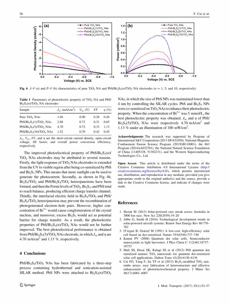
Table 1 Parameters of photoelectric property of TiO2 NA and PbS/
Bi2S3(n)/TiO2 NA electrodes
Sample Jsc (mA/cm2) Voc (V) FF g (%)
Pure TiO2 NAs 1.04 0.90 0.28 0.26
PbS/Bi2S3(1)/TiO2 NAs 2.88 0.72 0.31 0.65
PbS/Bi2S3(5)/TiO2 NAs 4.70 0.72 0.33 1.13
PbS/Bi2S3(10)/TiO2 NAs 1.52 0.70 0.42 0.45
Jsc, Voc, FF, and g are the short-circuit current density, open-circuit
voltage, fill factor, and overall power conversion efficiency,
respectively
56 F. Cai et al.
123 J. Mod. Transport. (2017) 25(1):52–57

7. Sun WT, Yu Y, Pan HY et al (2008) CdS quantum dots sensitized
TiO2 nanotube-array photoelectrodes. J Am Chem Soc
130(4):1124–1125
8. Gong D, Grimes CA, Varghese OK et al (2001) Titanium oxide
nanotube arrays prepared by anodic oxidation. J Mater Res
16(12):3331–3334
9. Cai F, Yang F, Zhang Y et al (2014) PbS sensitized TiO2 nan-
otube arrays with different sizes and filling degrees for enhancing
photoelectrochemical properties. Phys Chem Chem Phys
16(43):23967–23974
10. Rath AK, Bernechea M, Martinez L et al (2012) Solution-pro-
cessed inorganic bulk nano-heterojunctions and their application
to solar cells. Nat Photon 6(8):529–534
11. Zhao Q, Wang D, Peng L et al (2007) Surface photovoltage study
of photogenerated charges in ZnO nanorods array grown on ITO.
Chem Phys Lett 434(1):96–100
12. Peter LM, Wijayantha KGU, Riley DJ et al (2003) Band-edge
tuning in self-assembled layers of Bi2S3 nanoparticles used to
photosensitize nanocrystalline TiO2. J Phys Chem B 107(33):
8378–8381
13. Hyun BR, Zhong YW, Bartnik AC et al (2008) Electron injection
from colloidal PbS quantum dots into titanium dioxide nanopar-
ticles. ACS Nano 2(11):2206–2212
14. Pattantyus-Abraham AG, Kramer IJ, Barkhouse AR et al (2010)
Depleted-heterojunction colloidal quantum dot solar cells. ACS
Nano 4(6):3374–3380
15. Jiang J, Zhang X, Sun P et al (2011) ZnO/BiOI heterostructures:
photoinduced charge-transfer property and enhanced visible-light
photocatalytic activity. J Phys Chem C 115(42):20555–20564
Synthesis and photoelectrical performance of nanoscale PbS and Bi2S3 co-sensitized on TiO2… 57
123J. Mod. Transport. (2017) 25(1):52–57