
Synthesis and optical properties of copper nanoparticles prepared

Dynamic Article LinksC<Nanoscale
Cite this: Nanoscale, 2012, 4, 1422
www.rsc.org/nanoscale REVIEW
Dow
nloa
ded
by N
anya
ng T
echn
olog
ical
Uni
vers
ity o
n 18
Apr
il 20
12Pu
blis
hed
on 0
3 Ja
nuar
y 20
12 o
n ht
tp://
pubs
.rsc
.org
| do
i:10.
1039
/C1N
R11
612F
View Online / Journal Homepage / Table of Contents for this issue
Synthesis and optical properties of II–VI 1D nanostructures†
Muhammad Iqbal Bakti Utama,a Jun Zhang,a Rui Chen,a Xinlong Xu,b Dehui Li,a Handong Suna
and Qihua Xiong*ac
Received 29th October 2011, Accepted 18th November 2011
DOI: 10.1039/c1nr11612f
1D nanostructures from II–VI semiconductors have been demonstrated to exhibit outstanding optical
properties with strong promise for novel optoelectronic devices with augmented performance and
functionalities. Herein, we present a comprehensive review discussing important topics pertinent to the
fundamental properties and applications of II–VI 1D nanostructures. With practical applications in
mind, the considerations, principles and experimental techniques on the sample preparation of high
quality 1D nanostructures are highlighted. Fundamentals on the optical properties of II–VI materials,
along with relevant investigation techniques and recent progress in the field, are also extensively
discussed. With the steady development of their synthesis, characterization and device fabrication, it is
strongly expected that II–VI 1D nanostructures will assume a unique position in future technology.
aDivision of Physics and Applied Physics, School of Physical andMathematical Sciences, Nanyang Technological University, Singapore637371. E-mail: [email protected] Key Laboratory of Photoelectric Technology and FunctionalMaterials (Culture Base), National Photoelectric Technology andFunctional Materials and Application of Science and TechnologyInternational Cooperation Base, Northwest University, Xi’an, 710069,People’s Republic of ChinacDivision of Microelectronics, School of Electrical and ElectronicEngineering, Nanyang Technological University, Singapore 639798
† This article was submitted as part of a collection highlighting papers onthe ‘Recent Advances in Semiconductor Nanowires Research’ fromICMAT 2011.
Handong Sun
Dr Handong Sun obtained his
PhD in Physics from Hong
Kong University of Science and
Technology. He is now working
as an assistant professor in the
School of Physical and Mathe-
matical Sciences, Nanyang
Technological University
(NTU), Singapore. Before he
moved to NTU, he had been
working in the Institute of
Physical and Chemical Research
(RIKEN), Japan, and the
Institute of Photonics, The
University of Strathclyde, UK.
His current research interest is
focused on spectroscopic characterization of nanostructured
materials (inorganic, organic and hybrid structures), optoelec-
tronic devices, and plasmonics-based physics and devices.
1422 | Nanoscale, 2012, 4, 1422–1435
1. Introduction
Nanostructures, generally defined as systems in possession of at
least one dimension with a size between 1 to 100 nm, have
garnered immense attention from both curiosity-driven and
technologically-motivated research.1–6 Numerous fascinating
and groundbreaking advances have been demonstrated on the
potential applications of nanostructures, in part due to the
unique platform they provide to probe and manifest various size-
and structure-dependent material properties where the relevance
of quantum confinement effects is greater.
Qihua Xiong
Dr Qihua Xiong received his BS
degree from Wuhan University
and his MS degree from
Shanghai Institute of Applied
Physics, Chinese Academy of
Sciences. He received a PhD
degree in materials science
under the supervision of Prof.
Peter Eklund at Pennsylvania
State University in 2006. After
postdoctoral experience in Prof.
Charles Lieber’s group at Har-
vard University, he joined
Nanyang Technological Univer-
sity as a Nanyang assistant
professor in 2009. He is a Fellow
of the Singapore National Research Foundation. Prof. Xiong’s
research focuses on a range of topics in emerging nanomaterials
and nanostructures, from fundamental properties and device
applications in energy and biosensing.
This journal is ª The Royal Society of Chemistry 2012

Dow
nloa
ded
by N
anya
ng T
echn
olog
ical
Uni
vers
ity o
n 18
Apr
il 20
12Pu
blis
hed
on 0
3 Ja
nuar
y 20
12 o
n ht
tp://
pubs
.rsc
.org
| do
i:10.
1039
/C1N
R11
612F
View Online
In particular, nanostructures with quasi-one-dimensionality
(1D) have been proposed as active components in devices due to
their distinguished performance in electronics, photonics, and
optoelectronics. Among the examples of 1D nanostructures are
carbon nanotubes and semiconductor nanowires—which were
originally called ‘‘whiskers’’—along with the more recent vari-
ants such as nanobelts. However, the lack of reliable techniques
to produce uniform semiconducting carbon nanotubes has
impeded the industrial adoption of carbon nanotube technolo-
gies.2 Meanwhile, techniques to prepare high quality semi-
conducting nanowires with good control and reproducibility
have been made available by meticulous studies in the field within
the last decade.6 Exciting progress within the last few years in the
field of nanowires, as an important research front in nanotech-
nology, has strengthened the expectation of the pivotal role that
nanowires may possibly hold in the future.
II–VI semiconductors (zinc chalcogenides: ZnO, ZnS, ZnSe,
ZnTe; cadmium chalcogenides: CdS, CdSe, CdTe) are among
a class of materials that has been intensively studied in the field of
1D nanostructures.7–13 II–VI compounds are recognized as
promising materials in optoelectronics owing to their high
sensitivity and quantum efficiency.7 Additionally, the range of
their wide direct band gap implies a flexibility to fabricate
optoelectronic devices to work on various wavelengths of choice.
Nevertheless, the applications of bulk and films of II–VI semi-
conductors in industry have been hindered by the strict
requirement of epitaxial growth and substrate quality, control of
defects, and difficulty in doping as opposed to that of III–V
semiconductors. This situation is in direct contrast to 1D nano-
structures with good crystallinity and controlled doping which is
easier to prepare, facilitating fundamental studies as well as
possible device applications of II–VI nanostructures. This review
will therefore be focused on the preparation techniques of II–VI
1D nanostructures, the fundamental of optical properties rele-
vant to II–VI materials, and their applications in photonic and
optoelectronic devices.
2. Synthesis
The preparation of 1D nanostructures from II–VI semi-
conductors is a crucial stage for both the study of fundamental
properties and applications of the materials toward novel tech-
nologies. Thus, as a prerequisite, it is important to develop and
utilize reliable methods with the ability to produce well
controlled dimensions, morphology, and phase purity of nano-
structures with the desired functionality. In this regard, synthesis
approaches have been thoroughly explored and proposed as
a potential alternative to the production of nanostructures from
the more mature top-down fabrication techniques of the semi-
conductor industry. The advanced lithographic techniques of
top-down fabrication have not been able to produce nano-
materials with high throughput, in addition to the escalating
production and equipment costs for further structural minimi-
zation. Meanwhile, various synthesis techniques, adopting
a bottom-up paradigm by constructing structures from smaller
building blocks, have been reported to be able to generate 1D
nanostructures with high throughput at reasonable cost effec-
tiveness and good reproducibility.2,5 Nevertheless, the capability
of top-down processes is not to be depreciated, as the integration
This journal is ª The Royal Society of Chemistry 2012
of nanostructures into functional and scalable devices may still
necessitate the strong organization and spatial control of
lithography.
Synthesis of 1D nanostructures is performed by promoting
nucleation, crystallization, and growth in only one direction
while suppressing the 2D growth. The various strategies that
have been demonstrated for the growth of II–VI 1D nano-
structures can be categorized according to the reaction media
and precursors that are used during the synthesis process, which
is either a solution or vapor based technique.3 The great benefits
of vapor based techniques lie in their ability to produce very high
quality materials due to the high temperature involved in the
growth process, which allow the building blocks of the growth to
rearrange themselves to develop a long-range ordered crystalline
lattice.5,7 Furthermore, the experimental methods and technol-
ogies of vapor based techniques are already established, due to
their intensive use in semiconductor research and in industry,
and thus are compatible with device integration. In comparison,
solution based techniques allow a relatively lower temperature
(T < 400 �C) to produce nanostructures and is auspicious from
the economic standpoint.14,15 However, a major demerit of most
of the solution approaches is their difficulty to synthesize well-
crystallized nanowires by achieving simultaneously high
throughput, well-defined morphology and orientation, and
positioning control, thus strongly compromising their integra-
bility into optoelectronic devices and/or productivity.
In the following, we will discuss briefly the growth mechanism
and basic principles of the experimental techniques that have
been demonstrated to be generally applicable in producing high
quality II–VI 1D nanostructures while referring to representative
examples, whenever available.
2.1. Growth mechanism
The growth of II–VI 1D nanostructures by the vapor phase
typically follows the combination of two possible underlying
growth mechanisms: the vapor–liquid–solid and vapor–solid
mechanisms. A unique case of self-catalytic growth has also
received much attention which warrants further discussion in this
review.
2.1.1. Vapor–liquid–solid (VLS) growth. VLS growth16 is
well-accepted and among the most widely attributed mechanisms
for the growth of nanowires. An in situ transmission electron
microscopy (TEM) observation of nanowire growth with the
mechanism was demonstrated, which allowed an understanding
of the growth stages.17 The kinetics of the growth have also been
extensively examined.18–21 A schematic of VLS growth is shown
in Fig. 1. VLS growth is promoted by the presence of a metallic
particle droplet, whose role resembles the function of a catalyst in
a reaction, to direct the 1D growth. Thus, VLS growth is often
referred to as ‘‘catalytic’’ growth. The metallic particle then forms
a liquid alloy with the supplied vapor species of the materials to
be synthesized when the substrate temperature is elevated beyond
their eutectic temperature. The alloy thus becomes a preferred
adsorption site for vapor since the liquid surface has a high
sticking coefficient. Nucleation occurs when the alloy is super-
saturated, and the axial growth proceeds by precipitation at the
liquid alloy/solid interface. Meanwhile, secondary nucleation
Nanoscale, 2012, 4, 1422–1435 | 1423

Fig. 1 A schematic of the VLS mechanism for the growth of ME (M ¼Zn, Cd; E ¼ O, S, Se, Te) nanowires. The growth consists of four stages:
(a) formation of metallic catalyst particles, either from intentional
introduction to the substrate or due to segregation of the catalyst film at
high temperature; (b) formation of alloy with the incorporation of the
supplied ME vapor into the catalyst; (c) supersaturation in the alloy,
resulting in the precipitation of a nucleation centre of ME crystal; (d)
axial elongation, culminating into ME nanowires. The schematic repre-
sents a randomly-oriented growth of nanowires, which does not neces-
sitate any chemical or epitaxial relation to the substrate.
Dow
nloa
ded
by N
anya
ng T
echn
olog
ical
Uni
vers
ity o
n 18
Apr
il 20
12Pu
blis
hed
on 0
3 Ja
nuar
y 20
12 o
n ht
tp://
pubs
.rsc
.org
| do
i:10.
1039
/C1N
R11
612F
View Online
events are suppressed due to the higher energy involved than that
of crystal step growth, such that precipitation only occurs at the
single liquid/solid interface.17 1D growth continues until the
delivery of vapor reactant is discontinued or until the tempera-
ture is lowered below the eutectic temperature of the catalyst
alloy.
The presence of a metal-rich particle at the tip of the nanowire
is generally considered as an evidence of the VLS mechanism.16
However, the particle may also be detached due to interfacial
dewetting and thermal strain during the cooling process6 or
consumed during the growth.22 Noble metals (Ag, Pt, Ni, and
especially Au) are generally used as the catalyst particle, and an
appropriate choice of catalyst and growth temperature for the
synthesis of a certain II–VI compound can be determined with
the aid of pseudo-binary phase diagram.23 The catalyst particle
may also be used to control the diameter of the resulting nano-
wires, owing to the lateral growth confinement it provides.24
However, the metallic catalyst may diffuse from the tip22 and get
incorporated into the nanowire as a contaminant, which causes
concern, as such metallic contamination may affect the electronic
and optical properties of the nanowires.25
2.1.2. Self-catalytic growth. A special case of VLS growth
called self-catalytic growth arises when the constituent metallic
element of a compound serves as the catalyst, such as Zn for the
growth of zinc chalcogenides, thus eliminating the need for
a foreign catalyst which may evoke undesired contamination.26
To follow the mechanism, the catalyst can be generated by
pyrolysis of the source material at high vacuum and temperature
or through assisted decomposition by chemical reaction with the
carrier gas or additives. Similar to the conventional VLS mech-
anism, the catalyst particle may remain at the tip, as has been
demonstrated for ZnSe nanowire.27 However, the majority of
published works on self-catalytic growth reported the absence of
catalyst particle or any metal-rich site in the nanowires. Instead,
1424 | Nanoscale, 2012, 4, 1422–1435
tapered tip is often observed on the otherwise uniform diameter
nanowire.28–32 The lack of catalyst site can be ascribed to the
conversion of the catalyst into the material of the nanowire as
suggested from real-time TEM observation of the GaN nano-
wires growth.31 In absence of catalyst particle on the nanowire
product, the growth of nanowires without the use of foreign
metal catalyst can be attributed to self-catalytic growth by
consideration of the synthesis condition with regards to the
feasibility of catalyst generation and alloying with the vapor
reactant to follow VLS growth26–31 and the agreement of exper-
imental results with the kinetics and general characteristics of
a catalyzed growth.28 Improvements on the controllability of self-
catalytic mechanism, such as rational manipulation of the size
and positioning of the synthesized product, are still necessary to
fully exploit its demonstrated potential to produce high quality
and purity nanowires.
2.1.3. Vapor–solid (VS) growth. VS growth is a spontaneous
condensation process of vapor into solid material induced by the
decrease in Gibbs free energy from crystallization or the decrease
in supersaturation.12 VS growth is often invoked to explain the
growth of 1D nanostructures without any catalyst. Specifically,
the growth mechanism has been associated with the radial
thickening and tapering of nanowires, due to direct adsorption of
gas to the crystallized nanowires, and the growth of nanobelts.
Nanobelts33—also commonly called nanoribbons—are 1D
nanostructures that are subjected to a pronounced lateral growth
which accompanies the axial elongation, resulting in rectangular
cross sections. Nanobelts are generally conceived in the wurtzite
phase and numerous studies on nanobelts have been conve-
niently performed using II–VI materials, which can assume
a stable wurtzite phase under appropriate ambient conditions.34
Competition between surface energy minimization (which
favors the formation of nanobelts) and kinetics of crystal growth
(which controls the formation of nanowires) determines the
prevailing morphology during VS growth.35 When the vapor
precursor condensed at the substrate, the cation–anion adatoms
form a small nucleus while preserving the balance of local charge
and structural symmetry. Due to the difference in the kinetic
parameters for each crystal plane, anisotropic growth will result
and the nucleus will develop well-defined, low index crystallo-
graphic faces.9 However, when the temperature is sufficiently
high, accumulation of arriving atoms onto the smooth low-index
surface is prevented by the high diffusivity of the adatoms, thus
resulting in the expansion of surface area as more molecules stick
on the rougher growth front to form the nanobelts. Higher
supersaturation of the vapor phase has also been shown to
improve the 2D nucleation probability on the surface of
a nanowire to facilitate the growth of sheet-like structures,5,35
such that the dimension of a nanobelt can be controlled by
adjusting the growth temperature, the supersaturation ratio and
the growth time.
2.2. Experimental techniques
According to the setup and route to generate the vapor species,
the vapor based techniques commonly employed to synthesize
II–VI 1D nanostructures are thermal evaporation, laser-assisted
This journal is ª The Royal Society of Chemistry 2012

Fig. 2 (a) Typical experimental setup of the thermal evaporation
method to synthesize II–VI 1D nanostructures. Scanning electron
microscopy and high resolution transmission electron microscopy
(HRTEM) images of (b,c) ZnO nanowires, (d,e) CdSe nanowires, and
(f,g) ZnS nanobelts. The single crystallinity demonstrated by the uniform
fringes on the HRTEM images exemplified the high crystalline quality
that can be produced via the synthesis technique. (Fig. a,d,e are adapted
from ref. 28 with permission; Fig. b,c are adapted from ref. 36 with
permission; Fig. f,g are adapted from ref. 38 with permission.)
Dow
nloa
ded
by N
anya
ng T
echn
olog
ical
Uni
vers
ity o
n 18
Apr
il 20
12Pu
blis
hed
on 0
3 Ja
nuar
y 20
12 o
n ht
tp://
pubs
.rsc
.org
| do
i:10.
1039
/C1N
R11
612F
View Online
growth, molecular beam epitaxy (MBE), and metal–organic
chemical vapor deposition (MOCVD).
The thermal evaporation technique is the most popular
approach by virtue of its simplicity and effectiveness in synthe-
sizing diverse nanostructure morphologies from various mate-
rials.29 The technique uses powder or condensed source materials
that are vaporized at an elevated temperature, where the result-
ing vapor phase is transported and deposited onto a substrate
within a tube furnace. The growth parameters are carefully
chosen to form the intended products: (a) the type of source,
which may determine the phase and stoichiometry of the
product; (b) the vaporization temperature of the source mate-
rials, by considering the volatility of the source; (c) the pressure
of the growth chamber, to control the evaporation rate and
vapor pressure of the source; (d) the substrate temperature,
which will strongly determine the type of product to be obtained;
(e) the carrier gas and its flow rate, to allow certain chemical
reaction to occur during vapor transportation and to tune the
growth rate; and (f) the evaporation time, which will influence
the amount and size of the products. Nanowires and nanobelts
from all of the zinc chalcogenides27,29,36–43 and cadmium chalco-
genides28,44–47 have been produced with thermal evaporation by
following the VLS and VS mechanism. A typical schematic of the
setup and selection of electron micrograph of 1D nanostructures
produced with the method are given in Fig. 2.
Laser ablation is a process whereby a laser, either pulsed or
continuous wave, ablates a solid target containing the desired
elements to construct 1D nanostructures.48 The clusters of
vaporized material are thus collected by a cold finger or a wafer
inside a growth chamber with a controllable environment, where
the nanostructures are formed. The synthesis with laser ablation
has since been accomplished with a broader range of material,
including ZnO,30 ZnS,49–51 ZnSe, CdS, CdSe23 and CdTe,52
demonstrating the general applicability of the technique.
MBE is an epitaxial growth technique of semiconductor
compounds involving the reaction of thermal molecular beams
on a substrate under ultra-high vacuum conditions.53 When the
level of a vacuum is sufficiently high (�10�8 Pa), the mean free
path of molecules may exceed the separation between the source
and the substrate. The condition, called the Knudsen regime,
allows the generation of the molecular beam to produce struc-
tures with great control of precision, stoichiometry and growth
rate. Several groups have demonstrated the applicability of the
approach for the growth of ZnO,54 ZnS,55 ZnSe56 and ZnTe57
nanowires. Nevertheless, the issue of low growth rate, impracti-
cality of ultra high vacuum, and the requirement of very high
purity sources have to be resolved before MBE can receive wider
usages in the industrial production of nanowires.
MOCVD is a deposition technique where at least one of the
precursor gases is a metallic atom (such as Zn from ZnO)
attached to an organic compound with a sufficiently high vapor
pressure. The precursor gas experiences pyrolytic reactions in
a furnace at elevated temperatures, where the metallic atom is
deposited on the substrate while the organic compound is
removed from the reaction chamber. MOCVD-grown nanowires
have also been demonstrated for II–VI nanowires.58–63 But as
opposed to MBE, MOCVD can accomplish high volume growth
with its high intake of precursor gas and possibility to use a large
diameter substrate to harvest more nanostructures. Yet,
This journal is ª The Royal Society of Chemistry 2012
difficulties exist for the MOCVD process, such as the use of
highly toxic gases and complicated chemistry, causing undue
increases of production cost.
2.3. Epitaxial growth of nanowire arrays
An unique scenario may occur when the II–VI nanowires are
grown epitaxially on the surface of the substrate, i.e., when the
crystal building block of the II–VI material is arranged in orderly
fashion by consistently following a specific orientational relation.
When the fast growth plane of the nanowires is the plane to be
heterointerfaced with the substrate, the nanowires will grow
perpendicularly from the substrate into a nanowire array. Unlike
non-heteroepitaxial nanowires which are randomly oriented
(Fig. 1 and Fig. 2a), epitaxial nanowire arrays possess strong
alignment in the vertical direction (such as Fig. 2b). Such align-
ment can be utilized to harvest certain orientation-dependent
Nanoscale, 2012, 4, 1422–1435 | 1425

Fig. 3 Recombination processes in a semiconductor. (a) Band-to-band
recombination. (b) Band-to-acceptor transition. (c) Donor-to-valence
transition. (d) Donor-to-acceptor-pair transition. (e) Recombination via
a deep center. (f) Non-radiative recombination via an intermediate state.
(g) Band-to-band Auger recombination.
Dow
nloa
ded
by N
anya
ng T
echn
olog
ical
Uni
vers
ity o
n 18
Apr
il 20
12Pu
blis
hed
on 0
3 Ja
nuar
y 20
12 o
n ht
tp://
pubs
.rsc
.org
| do
i:10.
1039
/C1N
R11
612F
View Online
physical properties or phenomena exhibited by each nanowire,
which is essential in scalable applications.28 Additionally, in situ
growth in nanowire array structures also enables lattice relaxation
in lateral directions, allowing a larger critical height prior to defect
nucleations than that of similar lattice-mismatched epitaxial thin
films.64,65 Epitaxial nanowire arrays of II–VI materials were first
reported in ZnO,66 and have since been extensively studied in
a broad range of applications.
Conventional heteroepitaxy creates covalent bonds at the
heterointerface, thus requiring a matching of in-plane lattice
parameters between the nanowire and the substrate. Otherwise,
crystalline defects that are deleterious to the electronic and
photonic properties of the nanowires will occur. An epitaxial
strategy called van der Waals epitaxy has been proposed in thin
film growth67 to relieve the lattice matching requirements by
using substrates that promote van der Waals interaction—
instead of stronger chemical bonds—to connect the hetero-
junction. The van der Waals epitaxy has been attributed to the
growth of CdS, CdSe (Fig. 2a,b) and CdTe nanowire arrays with
excellent crystalline and luminescent qualities on a muscovite
mica substrate,28,68 thus also presenting a strong prospect for
application to other classes of compounds regardless of the
lattice mismatch.
3. Fundamentals of optical properties
3.1. Band structure
Optical transitions in semiconductors occur between the valence
and conduction bands. Therefore the studies of optical processes
and potential device applications require a complete knowledge
of the band structure. For II–VI semiconductors, the band
structure of wurtzite, zincblende, and rocksalt polytypes have
been theoretically investigated by varying the degree of
complexity. For wurtzite-type materials, the valence bands
originate from atomic p-like states whose symmetry is lower than
that of the diamond and zincblende cases. In comparison, the
minimum of the conduction band is s-like state with G7
symmetry.69 Spin–orbit coupling and crystal field split the
valence band into three sub-bands, resulting in a series of exciton
states which are denoted in the decreasing order of energy as A
(G9, also referred to as ‘‘heavy hole’’), B (G7, or ‘‘light hole’’), and
C (G7, or ‘‘split-off [SO] band’’).70,71 In order to observe different
excitonic transitions, one should consider the selection rules of
polarization.72 The transition energies of the intrinsic excitons
can be measured by employing low-temperature absorption,73
reflection,74 photoreflectance (PR)75 and photoluminescence (PL)
spectroscopy techniques.76,77 For example, the photon energy of
free excitons A and B (FX) in wurtzite ZnS nanowires was
determined by a low-temperature PL measurement to be 3.778
eV and 3.844 eV, respectively.78
3.2. Exciton and exciton complex
An exciton is a quasi-particle consisting of the bound state of an
electron and a hole interacting through the electrostatic
Coulombic force. Excitons behave similarly to a bosonic particle
freely moving in the crystal lattice of a semiconductor. In
comparison to free charge carriers, excitons demonstrate supe-
rior characteristics, such as large oscillator strength, narrow
1426 | Nanoscale, 2012, 4, 1422–1435
energy distribution of optical gain, and more varieties of possible
interactions with electrons or phonons. Moreover, excitons have
a dynamic electric dipole, which can couple with an electro-
magnetic wave, or light. In principle, this coupling between
a particle (exciton) and a field (electromagnetic cavity mode) can
be used to achieve zero threshold laser diodes.79 The exciton–
polariton coupling strength in the nanoscale is also significantly
enhanced from that in the bulk, as was recently reported with
CdS nanowire optical cavities.80 In 1D semiconductor materials,
we shall be concerned with Wannier excitons only.
There are two important optical processes which involve
emission of radiation from the semiconductors, namely, lumi-
nescence and inelastic scattering of light (also known as Raman
scattering). In a typical luminescent process, electrons in the
ground state are excited to a higher energy state, where after
some energy loss (i.e., relaxation) the excited electrons return to
the ground state by the emission of photons. There are several
categories of transitions that may happen in a PL process, as
shown in Fig. 3, depending on the sample and experimental
conditions such as temperature and excitation energy. For
instance, instead of a free carrier recombination processes, the
corresponding exciton recombination processes in the case of
a semiconductor with strong Coulombic interaction between the
electron and hole are FX, donor-bound excitons, and acceptor-
bound excitons.71 The donor or acceptor can be either neutral at
low temperature or ionized at high temperatures. The transition
energy difference between these excitonic emission and the free
carrier recombination processes is defined as the exciton binding
energy.
3.2.1. Exciton dynamics probed by steady state photo-lumi-
nescence. PL is used to study the optical properties of semi-
conductors. This is because PL provides very rich information on
both the intrinsic recombination processes and various radiative
recombination processes associated with imperfections of
a sample. With low temperature PL spectra, detailed information
about the semiconductor properties could be obtained, such as
exciton, phonon, and donor binding energy. Those properties are
very useful in giving a good picture of the optical quality of
semiconductor material.
Due to the difference in their densities of state (DOS), the
relative intensity of the defect and FX transition shows a very
different trend with the variation of excitation densities. As
shown in Fig. 4a, for ZnS nanowires at low temperature, the
This journal is ª The Royal Society of Chemistry 2012

Dow
nloa
ded
by N
anya
ng T
echn
olog
ical
Uni
vers
ity o
n 18
Apr
il 20
12Pu
blis
hed
on 0
3 Ja
nuar
y 20
12 o
n ht
tp://
pubs
.rsc
.org
| do
i:10.
1039
/C1N
R11
612F
View Online
shallow level emission demonstrates a faster saturation
compared with FXs and could not be resolved at moderate
excitation density.78 It is necessary to note that the PL emission
for II–VI 1D nanostructures may show a gradual red shift with
increased excitation density, which can be ascribed to laser
heating effect commonly observed in other classes of
nanostructures.81
With the change of the temperature of the sample, a thermal
shift of the band gap of semiconductors can be observed. The
band gap shrinkage is related to the thermal dilation of the
crystal lattice as well as electron–phonon interactions. As shown
in Fig. 4b, the temperature dependence of the emission can be
described by both the Varshni formula82 and the Bose–Einstein
expression.83 Furthermore, the temperature dependence of full
width at half-maximum (FWHM) can be described by electron–
phonon coupling.84 Therefore, the determination of the exciton-
longitudinal optical (LO) phonon coupling strength is thus made
possible.
3.2.2. Optical absorption and ultrafast spectroscopy. Excitons
are generated from optical absorption, which are the case for II–
VI nanostructures with high exciton binding energies. The non-
equilibrium carriers will select channels (either radiative or non-
radiative) to return to equilibrium.85 Ultrafast spectroscopy—
such as time-resolved PL spectroscopy, optical pump–probe
absorption, transmission, reflection or second harmonic gener-
ation (SHG) spectroscopy—is a highly sensitive technique that
can be used to monitor the processes experienced by those
carriers, to measure the time required by the carriers to traverse
each channel (i.e., exciton lifetime), and to understand the
mechanism of the energy loss from the carriers (e.g. by exciton–
exciton, exciton–phonon, electron–exciton, or electron–phonon
interactions).
Exciton lifetime is very sensitive to crystal quality, where the
lifetime is longer for samples with improved crystal quality. We
have reported a bi-exponential decay for high-quality ZnS
nanowires grown by pulsed laser vaporization.78 Room-temper-
ature time-resolved photoluminescence (TRPL) measurements
produced decay times of 0.45 and 2.7 ns, most probably repre-
senting the non-radiative and the intrinsic radiative lifetime of
the free excitons, respectively.
Fig. 4 (a) Evolution of the PL spectra of ZnS nanowires measured at 10
K under different excitation densities. The dashed vertical lines are
a guide for the eyes. (b) Temperature-dependent PL mapping of ZnS
nanowires measured at an excitation density �9.4 mW cm�2. All data
were normalized by FXB intensity and the dashed lines follow the peak
positions. (Adapted from ref. 78 with permission.)
This journal is ª The Royal Society of Chemistry 2012
Interestingly, the ultrafast processes of carriers under one-
dimensional confinement change dramatically from their bulk
counterparts. For example, the lifetime of both electrons and
holes decrease with decreasing nanowire diameter, which are
attributed to the surface effects.86 Comparison between ZnO
nanowires and films also suggests that the decay lifetime of
electron in nanowires is half as long as that in films, which results
from the increased electron interaction with interfaces and grain
boundaries in nanowires.87
The following discussion focuses on the unique physical
properties of II–VI 1D nanostructures, especially those of
nanowires and nanobelts, for optical absorption and ultrafast
phenomena as compared to bulk materials and nanocrystals.
Firstly, nanowire absorption showed sizeable absorption cross
sections in visible region in the range of 10�12 cm2 mm�1 to 10�10
cm2 mm�1, which is roughly one order larger than those of
nanocrystals and is thus valuable for photodetector and photo-
voltaic applications.88 These 1D materials have intrinsically
anisotropic physical properties.89 As an example, polarization-
sensitive photodetectors can be fabricated from CdSe nano-
wires,90 and the origin of this polarization sensitivity stems from
the potential dielectric contrast effects as well as from the
confinement-induced optical selection rules. By PL spectroscopy
from single CdSe and CdSe/CdS core/shell nanowires, Giblin
et al. suggested that even though confinement may play a role in
determining the magnitude of observed anisotropy values,
dielectric contrast influences appear to dominate the overall
nanowire anisotropy response.91
Secondly, as compared to bulk materials, II–VI 1D nano-
structures have very rich luminescent properties induced by
intrinsic defects. For example, during vapor transport chemical
vapor deposition synthesis, stoichiometric intrinsic defects such
as such as vacancies (VS and VCd), interstitials (SI and SCd), and
anti-sites (SCd and CdS) for CdS for CdS nanobelts will be
unintentionally formed, as vapor pressures for II and VI group
elements are very different at certain temperatures. Fig. 5a shows
a PL spectrum measured at 10 K for CdS nanobelts and fitted
with multiple Gaussian functions to determine the peak positions
and width. The emission peak at 2.543 eV is attributed to neutral
donor bound excitons, historically labeled as I2. The peak near
2.531 eV is from I1, referring to excitons bound to a neutral
acceptor. A series of peaks between 2.416–2.266 eV demonstrate
characteristic multiple phonon replicas with an energy spacing of
approximately one LO phonon (i.e. 37 meV). Fig. 5b summarizes
the energy levels of all intrinsic defects of interest obtained by
first principle method. First principle calculations verify that the
shallow donors in CdS are contributed by sulfur vacancies while
the acceptors are contributed by cadmium vacancies with a spin
imbalance (Fig. 5c).92 Our results suggest that these two vacancy
states facilitate the formation of I2 with a fast decay dynamics on
the order of tens to hundreds of picoseconds, and a donor–
acceptor-pair (DAP) exciton complex with a much slower decay
process on the order of hundreds of nanoseconds due to the spin
polarization. Fig. 5d depicts the transient PL decay (normalized)
of I2 in CdS nanobelts at 10 K with pump power ranging from 1
mW to 20 mW.At low pump power, only one decay lifetime s1 dueto the single exciton decay was observed. As power increases
further, a faster decay lifetime s2 due to multi-exciton interac-
tions appears. Fig. 5e displays three emission decays centered at
Nanoscale, 2012, 4, 1422–1435 | 1427

Fig. 5 (a) PL fine structure of CdS nanobelts at 10 K with a 325 nm He-Cd laser excitation. The blue curves are Gaussian line-shape decompositions
with each peak clearly labeled. (b) Summary of the band diagram of CdS showing the intrinsic defect levels from the first-principle calculation (units in
eV). (c) Calculated electronic density of states (DOS) of CdS with cadmium vacancy (upper panel) and sulphur vacancy (lower panel). The arrows
indicate the defect levels, which also reveal a spin imbalance in the case of cadmium vacancy. (d) Transient PL decay (normalized) of I2 in CdS nanobelts
at 10 Kwith pump power ranging from 1 mW to 20 mW.At low pump power, only one decay lifetime s1 was observed. As power increases further, a faster
decay lifetime s2 due to multiexciton interactions was observed. (e) The normalized transient PL decay dynamics of the DAP emission at three different
wavelengths. (Adapted from ref. 92 with permission.)
Dow
nloa
ded
by N
anya
ng T
echn
olog
ical
Uni
vers
ity o
n 18
Apr
il 20
12Pu
blis
hed
on 0
3 Ja
nuar
y 20
12 o
n ht
tp://
pubs
.rsc
.org
| do
i:10.
1039
/C1N
R11
612F
View Online
the three different wavelengths of the zero-phonon DAP PL
spectrum. Closer (more energetic) donor–acceptor pairs undergo
faster radiative recombination rates, which shows the charac-
teristic of DAP decay. Our results suggest the promise of engi-
neering the luminescent properties in terms of both energy and
lifetime of nanomaterials by controlling the species of defects.
Thirdly, the Auger process is an important non-radiative
channel, which happens frequently in nanostructures, especially
for the nanocrystals. The Auger recombination rates in 1D
systems are effectively suppressed, in contrast from those in
nanocrystals.93 The strongly reduced Auger decay rates lead to
increased optical gain-lifetime and hence efficient light amplifi-
cation, which will generate amplified spontaneous emission
(ASE) or lasing.94 This Auger process is population (pump
intensity) dependent in one-dimensional materials. Robel et al.
suggested that at high electron–hole pair densities, the dominant
process is bimolecular (exciton–exciton) Auger recombination,
while a three-carrier Auger relaxation mechanism which usually
happens in bulk materials and nanocrystals occurs under low
excitation intensity for small-diameter (between 6 and 8 nm)
CdSe nanowires.95
Fourthly, ASE or lasing in II–VI semiconductor nanowires or
nanobelts has been readily achieved with a threshold power
density ranging from several to tens of mJ cm�2 depending on the
quality and morphology of the sample.96 ASE takes place in the
absence of an optical cavity while lasing usually needs a cavity,
either formed as a natural cavity by the crystal facets or by
a mirror cavity, for further lasing from ASE process. The
ultrafast dynamics in the ASE (lasing) region are informative to
understand the fundamentals of nanophotonics. Time-resolved
1428 | Nanoscale, 2012, 4, 1422–1435
SHG and PL spectroscopy were first utilized to probe the
dynamics of single ZnO nanowire and nanobelt lasers.97 They
observed an 80 ps free exciton decay channel and a less than 10 ps
stimulated emission involving a quick channel. Recently, we also
observed the ASE process in CdS nanobelts, with stimulated
emission on the time scale of 20 ps.92 Dynamic competition
between I2 and DAP has been identified, which suggests that
compensation of acceptor levels in CdS nanobelts is required to
achieve ASE. This ASE process can also be influenced by the
band gap renormalization with wavelength-dependent lasing
time dynamics, showing different lifetime as the morphology of
the sample changes.96,98
3.3. Lasing
A variety of optically pumped stimulated emissions (SE) have
been observed by many researchers from II–VI semiconductors.
As discussed above, excitonic emission is preferable for
decreasing the threshold for lasing. In II–VI semiconductors, the
exciton binding energy of ZnO (�60 meV),76 ZnS (�40 meV),99
and CdS (�28 meV)100 is larger than the thermal energy at room
temperature, thus enabling the observation of excitonic emission
at room temperature. It is well known that the lasing action needs
a proper optical cavity to provide positive feedback. In the case
of one-dimensional nanowires, this is usually realized by either
pumping on a single wire (in Fabry–P�erot or whispering gallery
mode lasing) or observing random lasing in an ensemble of
densely distributed nanowires, both of which require not only
a proper pumping scheme but also a well controlled sample
manipulation or fabrication.
This journal is ª The Royal Society of Chemistry 2012

Fig. 7 The emission spectra fromCdSe NWs at room temperature under
different excitation densities. The inset shows the dependence of the PL
integrated intensity on the laser excitation density. (Adapted from ref. 68
with permission.)
Dow
nloa
ded
by N
anya
ng T
echn
olog
ical
Uni
vers
ity o
n 18
Apr
il 20
12Pu
blis
hed
on 0
3 Ja
nuar
y 20
12 o
n ht
tp://
pubs
.rsc
.org
| do
i:10.
1039
/C1N
R11
612F
View Online
The near band emission of ZnO nanowires is located at �380
nm at room temperature. The first observation of lasing from
ZnO nanowire arrays was reported by Huang et al.66 The sample
was pumped byNd:YAG laser (266 nm, 3 ns pulse width) and the
emission was collected in the direction normal to the nanowires,
along the c-axis. As shown in Fig. 6a, when the excitation density
exceeds the threshold, sharp peaks with linewidths as small as 0.3
nm emerged in the emission spectra. The lasing cavity of these
nanowire arrays was ascribed to the natural cavity formed by the
two ends of the entire nanowires (Fig. 6c).
It is also possible that the laser cavity is formed by the entire
array, leading to lasing in arbitrary pathways with the nano-
wires as scattering centers. This phenomenon is known as
random lasing and was first observed in ZnO powder
samples.101 Random lasing in II–VI nanowires was previously
more commonly demonstrated in the UV regime with
ZnO.102,103 The random lasing in the near IR regime had not
been observed until very recently when high quality CdSe
nanowire arrays were achieved by the van der Waals epitaxy
mechanism. As shown in Fig. 7, near-infrared (NIR) random
lasing was observed at room temperature in CdSe nanowire
arrays grown on mica.68 Compared with conventional lasers,
random lasing from semiconductor NWs exhibits remarkable
differences. First of all, the random lasing can be observed
from all directions, and the spectrum recorded from a different
angle is different. Secondly, the lasing threshold strongly
depends on the excitation area. In the case of CdSe nanowires,
the pump area (Ath) and pump threshold (Pth) shows a A2/3th z
KP�1th relationship, where K is a constant.104,105 This indicates
that the vertically aligned CdSe nanowires should behave like
a quasi-3D random medium. Based on a similar concept,
random lasing in randomly-oriented nanobelts has also been
demonstrated in CdS.106
Fig. 6 (a) Emission spectra from nanowire arrays below (line a) and
above (line b and inset) the lasing threshold. The pump powers for these
spectra are 20, 100, and 150 kW cm�2, respectively. The spectra are offset
for easy comparison. (b) Integrated emission intensity from nanowires as
a function of optical pumping energy intensity. (c) Schematic illustration
of a nanowire as a resonance cavity with two naturally faceted hexagonal
end faces acting as reflecting mirrors. (Adapted from ref. 66 with
permission.)
This journal is ª The Royal Society of Chemistry 2012
3.4. Phonons
Phonons are quanta of lattice vibrations. They play a major role
in electrical, thermal, and optical properties of solid bulk mate-
rials and nanostructures107 as phonons carry energy and interact
with electrons via electron–phonon interaction and interact
among themselves via phonon–phonon interactions. The
importance of phonons are also demonstrated in various inter-
esting phenomena, such as phonon confinement in SNWs,108,109
phonon bottleneck effects in nanowires and quantum dot opto-
electronic devices,110 resonant Raman scattering,111 and deter-
mination of carriers mobility.107
Theoretically, the frequency and dispersion relation of
phonons can be obtained by solving the lattice dynamics equa-
tion. The vibrational modes of phonons can be either Raman-
active or IR-active. Hence, infrared absorption and Raman
spectroscopy are complementary in the experimental measure-
ment and assignment of vibrational modes.
Since the Raman effect was discovered more than 80 years
ago,112 Raman spectroscopy has become one of the most
powerful spectroscopic tools to study phonons and other element
excitations in condensed matter physics. Raman spectroscopy is
non-destructive and highly sensitive, where it can detect objects
on the order of a few nanometres, at a broad excitation energy
range (UV-NIR).
The first-order inelastic Raman scattering processes are two-
photon events that involve the simultaneous annihilation of an
incident photon and the creation of a scattered photon, mediated
by electron–photon and electron–phonon interactions.113 In this
process, the conservation of energy and momentum must be
satisfied simultaneously. In the visible and near infrared regime,
the momentum of the photon (wave vector) is less than 106 cm�1.
This wave vector is much smaller by about two orders of
magnitude than that of phonons, which corresponds to the
Brillouin zone boundary of typical crystals. Thus, the first-order
processes only access phonons and other elementary excitations
at or near the centre of the Brillouin zone, i.e., the well-known
q ¼ 0 Raman selection rule.
For one-dimensional nanowires, the shape of phonon disper-
sion relation can be obtained by folding the Brillouin zone of
bulk materials. However, some new modes (e.g. radial breathing
modes, RBMs) will emerge when the diameter of the wires is
Nanoscale, 2012, 4, 1422–1435 | 1429
Dow
nloa
ded
by N
anya
ng T
echn
olog
ical
Uni
vers
ity o
n 18
Apr
il 20
12Pu
blis
hed
on 0
3 Ja
nuar
y 20
12 o
n ht
tp://
pubs
.rsc
.org
| do
i:10.
1039
/C1N
R11
612F
View Online
smaller than a certain critical size, apart from the notable
confined phonon states in the quantum size regime. Another
issue is the interface and surface vibrations, such as surface
phonons in nanostructures, which becomes more significant due
to the increase of the surface-to-volume ratio with the decrease of
size. The observation of surface optical phonons in nanowires
usually indicates some type of translational symmetry breaking,
since surface optical modes are not generally activated due to
momentum conservation.
3.4.1. Radial breathing modes (RBMs). The RBMs of
a nanowire are similar to the RBMs of carbon nanotubes
(CNTs),111 except that the vibration is considered for a solid
cylinder instead of a hollow tube. The mode corresponds to the
vibration of the atoms in the radial direction, as if the wire/tube
were breathing, where the frequency is strongly diameter
sensitive.
The frequency of RBMs based on elastic theory for a long
isotropic cylindrical nanowire, e.g., in silicon, is given by:114,115
u ¼ nl
R
ffiffiffiffiffiffiffiffiffiffiffiffiffiffiffiffiffi8ð1� rÞð2� rÞ
s(1)
where n is the longitudinal sound velocity, R is the radius of the
nanowire, and r ¼ m/l + 2m, with (l,m) being the elastic constant
of materials. Eqn (1) indicates that the radial breathing mode
frequency follows a 1/R behavior, which is similar to the results
of RBMs in CNTs. Recent ab initio calculation shows the
frequency evolution of RBM can be fitted by the following
empirical power law for silicon nanowires:116,117
uRBMðdÞ ¼ 1
ARþ B(2)
whereA and B are the fitting parameters. Compared to elemental
semiconductor such as silicon, a more rapid progress in the
experimental study of RBMs in II–VI nanowires was witnessed
due to the wide availability of techniques to prepare nearly
monodisperse II–VI nanowires at a small diameter. For instance,
the presence of RBMs has been experimentally confirmed in
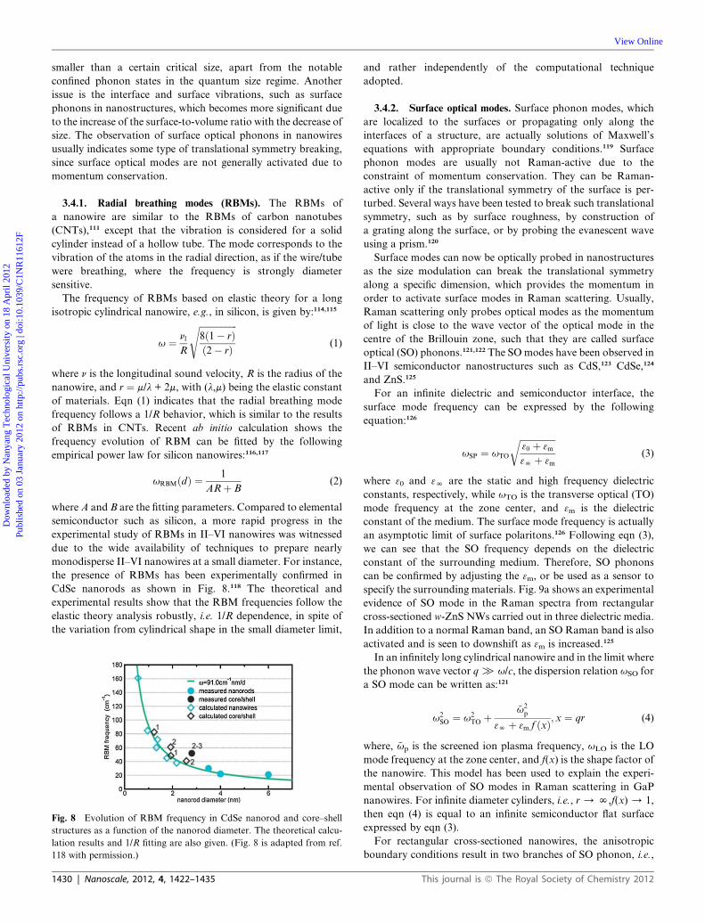
CdSe nanorods as shown in Fig. 8.118 The theoretical and
experimental results show that the RBM frequencies follow the
elastic theory analysis robustly, i.e. 1/R dependence, in spite of
the variation from cylindrical shape in the small diameter limit,
Fig. 8 Evolution of RBM frequency in CdSe nanorod and core–shell
structures as a function of the nanorod diameter. The theoretical calcu-
lation results and 1/R fitting are also given. (Fig. 8 is adapted from ref.
118 with permission.)
1430 | Nanoscale, 2012, 4, 1422–1435
and rather independently of the computational technique
adopted.
3.4.2. Surface optical modes. Surface phonon modes, which
are localized to the surfaces or propagating only along the
interfaces of a structure, are actually solutions of Maxwell’s
equations with appropriate boundary conditions.119 Surface
phonon modes are usually not Raman-active due to the
constraint of momentum conservation. They can be Raman-
active only if the translational symmetry of the surface is per-
turbed. Several ways have been tested to break such translational
symmetry, such as by surface roughness, by construction of
a grating along the surface, or by probing the evanescent wave
using a prism.120
Surface modes can now be optically probed in nanostructures
as the size modulation can break the translational symmetry
along a specific dimension, which provides the momentum in
order to activate surface modes in Raman scattering. Usually,
Raman scattering only probes optical modes as the momentum
of light is close to the wave vector of the optical mode in the
centre of the Brillouin zone, such that they are called surface
optical (SO) phonons.121,122 The SOmodes have been observed in
II–VI semiconductor nanostructures such as CdS,123 CdSe,124
and ZnS.125
For an infinite dielectric and semiconductor interface, the
surface mode frequency can be expressed by the following
equation:126
uSP ¼ uTO
ffiffiffiffiffiffiffiffiffiffiffiffiffiffiffiffi30 þ 3m
3N þ 3m
r(3)
where 30 and 3N are the static and high frequency dielectric
constants, respectively, while uTO is the transverse optical (TO)
mode frequency at the zone center, and 3m is the dielectric
constant of the medium. The surface mode frequency is actually
an asymptotic limit of surface polaritons.126 Following eqn (3),
we can see that the SO frequency depends on the dielectric
constant of the surrounding medium. Therefore, SO phonons
can be confirmed by adjusting the 3m, or be used as a sensor to
specify the surrounding materials. Fig. 9a shows an experimental
evidence of SO mode in the Raman spectra from rectangular
cross-sectioned w-ZnS NWs carried out in three dielectric media.
In addition to a normal Raman band, an SO Raman band is also
activated and is seen to downshift as 3m is increased.125
In an infinitely long cylindrical nanowire and in the limit where
the phonon wave vector q[ u/c, the dispersion relation uSO for
a SO mode can be written as:121
u2SO ¼ u2
TO þ ~u2p
3N þ 3m f ðxÞ; x ¼ qr (4)
where, ~up is the screened ion plasma frequency, uLO is the LO
mode frequency at the zone center, and f(x) is the shape factor of
the nanowire. This model has been used to explain the experi-
mental observation of SO modes in Raman scattering in GaP
nanowires. For infinite diameter cylinders, i.e., r/N,f(x)/ 1,
then eqn (4) is equal to an infinite semiconductor flat surface
expressed by eqn (3).
For rectangular cross-sectioned nanowires, the anisotropic
boundary conditions result in two branches of SO phonon, i.e.,
This journal is ª The Royal Society of Chemistry 2012
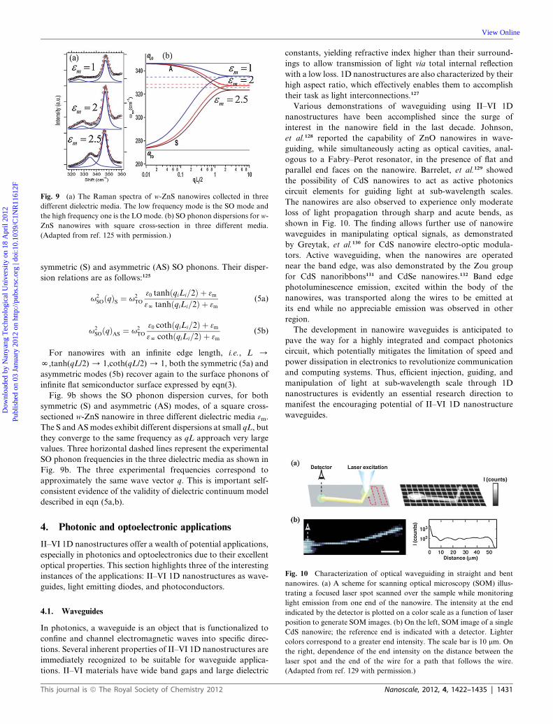
Fig. 9 (a) The Raman spectra of w-ZnS nanowires collected in three
different dielectric media. The low frequency mode is the SO mode and
the high frequency one is the LO mode. (b) SO phonon dispersions for w-
ZnS nanowires with square cross-section in three different media.
(Adapted from ref. 125 with permission.)
Dow
nloa
ded
by N
anya
ng T
echn
olog
ical
Uni
vers
ity o
n 18
Apr
il 20
12Pu
blis
hed
on 0
3 Ja
nuar
y 20
12 o
n ht
tp://
pubs
.rsc
.org
| do
i:10.
1039
/C1N
R11
612F
View Online
symmetric (S) and asymmetric (AS) SO phonons. Their disper-
sion relations are as follows:125
u2SOðqÞS ¼ u2
TO
30 tanhðqiLi=2Þ þ 3m
3N tanhðqiLi=2Þ þ 3m(5a)
u2SOðqÞAS ¼ u2
TO
30 cothðqiLi=2Þ þ 3m
3N cothðqiLi=2Þ þ 3m(5b)
For nanowires with an infinite edge length, i.e., L /
N,tanh(qL/2)/ 1,coth(qL/2)/ 1, both the symmetric (5a) and
asymmetric modes (5b) recover again to the surface phonons of
infinite flat semiconductor surface expressed by eqn(3).
Fig. 9b shows the SO phonon dispersion curves, for both
symmetric (S) and asymmetric (AS) modes, of a square cross-
sectioned w-ZnS nanowire in three different dielectric media 3m.
The S and ASmodes exhibit different dispersions at small qL, but
they converge to the same frequency as qL approach very large
values. Three horizontal dashed lines represent the experimental
SO phonon frequencies in the three dielectric media as shown in
Fig. 9b. The three experimental frequencies correspond to
approximately the same wave vector q. This is important self-
consistent evidence of the validity of dielectric continuum model
described in eqn (5a,b).
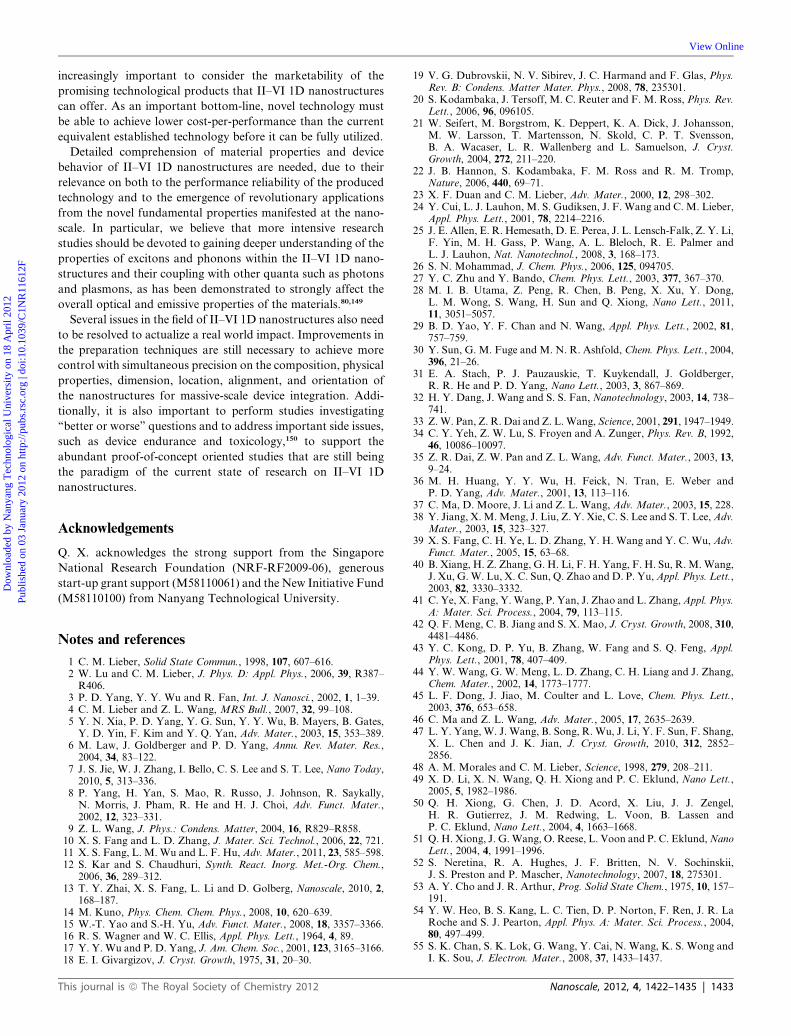
Fig. 10 Characterization of optical waveguiding in straight and bent
nanowires. (a) A scheme for scanning optical microscopy (SOM) illus-
4. Photonic and optoelectronic applications
II–VI 1D nanostructures offer a wealth of potential applications,
especially in photonics and optoelectronics due to their excellent
optical properties. This section highlights three of the interesting
instances of the applications: II–VI 1D nanostructures as wave-
guides, light emitting diodes, and photoconductors.
trating a focused laser spot scanned over the sample while monitoringlight emission from one end of the nanowire. The intensity at the end
indicated by the detector is plotted on a color scale as a function of laser
position to generate SOM images. (b) On the left, SOM image of a single
CdS nanowire; the reference end is indicated with a detector. Lighter
colors correspond to a greater end intensity. The scale bar is 10 mm. On
the right, dependence of the end intensity on the distance between the
laser spot and the end of the wire for a path that follows the wire.
(Adapted from ref. 129 with permission.)
4.1. Waveguides
In photonics, a waveguide is an object that is functionalized to
confine and channel electromagnetic waves into specific direc-
tions. Several inherent properties of II–VI 1D nanostructures are
immediately recognized to be suitable for waveguide applica-
tions. II–VI materials have wide band gaps and large dielectric
This journal is ª The Royal Society of Chemistry 2012
constants, yielding refractive index higher than their surround-
ings to allow transmission of light via total internal reflection
with a low loss. 1D nanostructures are also characterized by their
high aspect ratio, which effectively enables them to accomplish
their task as light interconnections.127
Various demonstrations of waveguiding using II–VI 1D
nanostructures have been accomplished since the surge of
interest in the nanowire field in the last decade. Johnson,
et al.128 reported the capability of ZnO nanowires in wave-
guiding, while simultaneously acting as optical cavities, anal-
ogous to a Fabry–Perot resonator, in the presence of flat and
parallel end faces on the nanowire. Barrelet, et al.129 showed
the possibility of CdS nanowires to act as active photonics
circuit elements for guiding light at sub-wavelength scales.
The nanowires are also observed to experience only moderate
loss of light propagation through sharp and acute bends, as
shown in Fig. 10. The finding allows further use of nanowire
waveguides in manipulating optical signals, as demonstrated
by Greytak, et al.130 for CdS nanowire electro-optic modula-
tors. Active waveguiding, when the nanowires are operated
near the band edge, was also demonstrated by the Zou group
for CdS nanoribbons131 and CdSe nanowires.132 Band edge
photoluminescence emission, excited within the body of the
nanowires, was transported along the wires to be emitted at
its end while no appreciable emission was observed in other
region.
The development in nanowire waveguides is anticipated to
pave the way for a highly integrated and compact photonics
circuit, which potentially mitigates the limitation of speed and
power dissipation in electronics to revolutionize communication
and computing systems. Thus, efficient injection, guiding, and
manipulation of light at sub-wavelength scale through 1D
nanostructures is evidently an essential research direction to
manifest the encouraging potential of II–VI 1D nanostructure
waveguides.
Nanoscale, 2012, 4, 1422–1435 | 1431

Dow
nloa
ded
by N
anya
ng T
echn
olog
ical
Uni
vers
ity o
n 18
Apr
il 20
12Pu
blis
hed
on 0
3 Ja
nuar
y 20
12 o
n ht
tp://
pubs
.rsc
.org
| do
i:10.
1039
/C1N
R11
612F
View Online
4.2. Electroluminescence (EL) and light emitting diodes
(LEDs)
EL is a phenomenon in which electricity drives light emission,
including carrier injection and radiative recombination. EL has
attracted a great deal of attention due to the fact that it can be
easily integrated into electronic devices to provide wide appli-
cations including in lighting and displays. Studies are currently
being performed to resolve the main challenges in improving the
conversion efficiency and device stability.
II–VI semiconducting compound nanowires and nanobelts are
ideal candidates for EL because of their inherent properties such
as a direct band gap, large band gap coverage, high crystalline
quality, large surface area, and small size. A direct band gap is
the essential requirement for light emission while large band gap
coverage enables them to be utilized at various wavelengths from
IR to near UV. High crystalline quality can enhance the radiative
recombination rate while large surface area would provide the
flexibility to manipulate the surface. Besides, it is possible to
create a smaller beam spot due to the small size of the nanowires
and nanobelts.
Lieber and co-workers have realized electrically driven light
emission on n-CdS nanowire on a p-Si substrate.133 The Fabry–
Perot cavity modes formed inside nanowires lead to a series of
peaks at the emission spectra. Green light lasing can also be
obtained with a further increment of the bias, as shown in
Fig. 11. The heterostructure of n-CdS nanowire/p-Si nanowire
junctions also has been adopted to realize electrically driven light
emission.134 Additionally, multicolored light using the same p-
type nanowires can be achieved by changing the choice of n-type
nanowire. Hayden et al.135 utilized an n-CdS shell/p-Si core
structure to fabricate an LED. In addition, CdSe nanowires136
and nanobelts137 have also been made into devices to investigate
their respective EL properties. Besides, flexible single ZnO
nanowire light emitting diodes have also been demonstrated.138
4.3. Photoconductivity: photodetection and switching
When a beam of light shines on a semiconductor or an insulator,
the electrical conductance may either increase (positive photo-
conductivity) or decrease (negative photoconductivity). Great
efforts have been dedicated into this research field to find new
photoconducting materials with improved performance due to
their wide applications, such as in photodetectors, solar cells and
sensors.
Fig. 11 (a) Schematic of the n-CdS nanowire/p-Si device. (b) Electro-
luminescence spectra obtained from the device depicted in (a) with
injection currents of 120 mA (red) and 210 mA (green). (c) Electrolu-
minescence spectra from the device with injection currents of 200 mA
(red) and 280 mA (green) at 8 K. (Adapted from ref. 133 with
permission.)
1432 | Nanoscale, 2012, 4, 1422–1435
Utilizing a material in its nanoscale form has been shown to
improve greatly the photoconductivity in both carrier generation
and transport, which are the two processes involved in the study
of photoconductivity. The high crystalline quality of nano-
structures can reduce the scattering during the transport process
while the large surface-to-volume ratio can strengthen the
significance of surface states, which would enhance the recom-
bination rate and thus increase the response speed. In addition,
the large surface-to-volume ratio also improves the trapping of
charge carrier to enhance the sensitivity further, due to the more
pronounced depletion region near the surface.
Yang and co-workers initiated the research on photoconduc-
tivity of II–VI nanowires by studying ZnO,139 where the group
reported IV curves with and without illumination and the
switching characteristics as shown in Fig. 12. The large photo-
sensitivity and high on–off ratio demonstrates that nanowires are
good candidates for photoconductors. Since then, the photo-
conducting property of a wide variety of nanowires and nano-
belts—which is characterized by the sensitivity, spectral
response, response speed and switch characteristics—have been
studied in great detail, owing to the rapidly developing synthesis
techniques of 1D nanostructures. The photoconductivity of II–
IV 1D nanostructures such as that from ZnO,139,140 CdS,141–144
CdSe,90 CdTe, ZnSe,145 and ZnS146,147 have been intensively
investigated. Various fascinating phenomena on the photo-
conducting properties of II–VI 1D nanostructures have also been
studied, including the improvement of photosensitivity by
exploiting a Fabry–Perot cavity between a nanowire or nanobelt
photodetector with the substrate90 and a polarization-dependent
sensitivity, as was observed in CdSe90 and CdTe nanowires148 due
to the high aspect ratio of nanowires.
5. Conclusions
We have provided an overview of the material preparation
techniques, the fundamentals of exceptional optical properties
and the promising optoelectronic applications of II–VI 1D
nanostructures, along with brief highlights of prominent past
research activities in the field. With the rapid progress of the
research in the field within only the last decade, it is thus
Fig. 12 (a) I–V curves of a single ZnO nanowire under 365 nm, 0.3 mW
cm�2 UV light illumination, exhibiting the dark and photocurrent
property of the structure. The inset shows an FE-SEM image of a 60 nm
ZnO nanowire bridging four Au electrodes. (b) Reversible switching of
a ZnO nanowire between low and high conductivity states when the
handheld UV-lamp was turned on and off. The bias on the nanowire is
1 V. (Adapted from ref. 139 with permission.)
This journal is ª The Royal Society of Chemistry 2012
Dow
nloa
ded
by N
anya
ng T
echn
olog
ical
Uni
vers
ity o
n 18
Apr
il 20
12Pu
blis
hed
on 0
3 Ja
nuar
y 20
12 o
n ht
tp://
pubs
.rsc
.org
| do
i:10.
1039
/C1N
R11
612F
View Online
increasingly important to consider the marketability of the
promising technological products that II–VI 1D nanostructures
can offer. As an important bottom-line, novel technology must
be able to achieve lower cost-per-performance than the current
equivalent established technology before it can be fully utilized.
Detailed comprehension of material properties and device
behavior of II–VI 1D nanostructures are needed, due to their
relevance on both to the performance reliability of the produced
technology and to the emergence of revolutionary applications
from the novel fundamental properties manifested at the nano-
scale. In particular, we believe that more intensive research
studies should be devoted to gaining deeper understanding of the
properties of excitons and phonons within the II–VI 1D nano-
structures and their coupling with other quanta such as photons
and plasmons, as has been demonstrated to strongly affect the
overall optical and emissive properties of the materials.80,149
Several issues in the field of II–VI 1D nanostructures also need
to be resolved to actualize a real world impact. Improvements in
the preparation techniques are still necessary to achieve more
control with simultaneous precision on the composition, physical
properties, dimension, location, alignment, and orientation of
the nanostructures for massive-scale device integration. Addi-
tionally, it is also important to perform studies investigating
‘‘better or worse’’ questions and to address important side issues,
such as device endurance and toxicology,150 to support the
abundant proof-of-concept oriented studies that are still being
the paradigm of the current state of research on II–VI 1D
nanostructures.
Acknowledgements
Q. X. acknowledges the strong support from the Singapore
National Research Foundation (NRF-RF2009-06), generous
start-up grant support (M58110061) and the New Initiative Fund
(M58110100) from Nanyang Technological University.
Notes and references
1 C. M. Lieber, Solid State Commun., 1998, 107, 607–616.2 W. Lu and C. M. Lieber, J. Phys. D: Appl. Phys., 2006, 39, R387–R406.
3 P. D. Yang, Y. Y. Wu and R. Fan, Int. J. Nanosci., 2002, 1, 1–39.4 C. M. Lieber and Z. L. Wang, MRS Bull., 2007, 32, 99–108.5 Y. N. Xia, P. D. Yang, Y. G. Sun, Y. Y. Wu, B. Mayers, B. Gates,Y. D. Yin, F. Kim and Y. Q. Yan, Adv. Mater., 2003, 15, 353–389.
6 M. Law, J. Goldberger and P. D. Yang, Annu. Rev. Mater. Res.,2004, 34, 83–122.
7 J. S. Jie, W. J. Zhang, I. Bello, C. S. Lee and S. T. Lee, Nano Today,2010, 5, 313–336.
8 P. Yang, H. Yan, S. Mao, R. Russo, J. Johnson, R. Saykally,N. Morris, J. Pham, R. He and H. J. Choi, Adv. Funct. Mater.,2002, 12, 323–331.
9 Z. L. Wang, J. Phys.: Condens. Matter, 2004, 16, R829–R858.10 X. S. Fang and L. D. Zhang, J. Mater. Sci. Technol., 2006, 22, 721.11 X. S. Fang, L. M. Wu and L. F. Hu, Adv. Mater., 2011, 23, 585–598.12 S. Kar and S. Chaudhuri, Synth. React. Inorg. Met.-Org. Chem.,
2006, 36, 289–312.13 T. Y. Zhai, X. S. Fang, L. Li and D. Golberg, Nanoscale, 2010, 2,
168–187.14 M. Kuno, Phys. Chem. Chem. Phys., 2008, 10, 620–639.15 W.-T. Yao and S.-H. Yu, Adv. Funct. Mater., 2008, 18, 3357–3366.16 R. S. Wagner and W. C. Ellis, Appl. Phys. Lett., 1964, 4, 89.17 Y. Y. Wu and P. D. Yang, J. Am. Chem. Soc., 2001, 123, 3165–3166.18 E. I. Givargizov, J. Cryst. Growth, 1975, 31, 20–30.
This journal is ª The Royal Society of Chemistry 2012
19 V. G. Dubrovskii, N. V. Sibirev, J. C. Harmand and F. Glas, Phys.Rev. B: Condens. Matter Mater. Phys., 2008, 78, 235301.
20 S. Kodambaka, J. Tersoff, M. C. Reuter and F. M. Ross, Phys. Rev.Lett., 2006, 96, 096105.
21 W. Seifert, M. Borgstrom, K. Deppert, K. A. Dick, J. Johansson,M. W. Larsson, T. Martensson, N. Skold, C. P. T. Svensson,B. A. Wacaser, L. R. Wallenberg and L. Samuelson, J. Cryst.Growth, 2004, 272, 211–220.
22 J. B. Hannon, S. Kodambaka, F. M. Ross and R. M. Tromp,Nature, 2006, 440, 69–71.
23 X. F. Duan and C. M. Lieber, Adv. Mater., 2000, 12, 298–302.24 Y. Cui, L. J. Lauhon, M. S. Gudiksen, J. F. Wang and C. M. Lieber,
Appl. Phys. Lett., 2001, 78, 2214–2216.25 J. E. Allen, E. R. Hemesath, D. E. Perea, J. L. Lensch-Falk, Z. Y. Li,
F. Yin, M. H. Gass, P. Wang, A. L. Bleloch, R. E. Palmer andL. J. Lauhon, Nat. Nanotechnol., 2008, 3, 168–173.
26 S. N. Mohammad, J. Chem. Phys., 2006, 125, 094705.27 Y. C. Zhu and Y. Bando, Chem. Phys. Lett., 2003, 377, 367–370.28 M. I. B. Utama, Z. Peng, R. Chen, B. Peng, X. Xu, Y. Dong,
L. M. Wong, S. Wang, H. Sun and Q. Xiong, Nano Lett., 2011,11, 3051–5057.
29 B. D. Yao, Y. F. Chan and N. Wang, Appl. Phys. Lett., 2002, 81,757–759.
30 Y. Sun, G. M. Fuge and M. N. R. Ashfold, Chem. Phys. Lett., 2004,396, 21–26.
31 E. A. Stach, P. J. Pauzauskie, T. Kuykendall, J. Goldberger,R. R. He and P. D. Yang, Nano Lett., 2003, 3, 867–869.
32 H. Y. Dang, J. Wang and S. S. Fan, Nanotechnology, 2003, 14, 738–741.
33 Z.W. Pan, Z. R. Dai and Z. L.Wang, Science, 2001, 291, 1947–1949.34 C. Y. Yeh, Z. W. Lu, S. Froyen and A. Zunger, Phys. Rev. B, 1992,
46, 10086–10097.35 Z. R. Dai, Z. W. Pan and Z. L. Wang, Adv. Funct. Mater., 2003, 13,
9–24.36 M. H. Huang, Y. Y. Wu, H. Feick, N. Tran, E. Weber and
P. D. Yang, Adv. Mater., 2001, 13, 113–116.37 C. Ma, D. Moore, J. Li and Z. L. Wang, Adv. Mater., 2003, 15, 228.38 Y. Jiang, X. M.Meng, J. Liu, Z. Y. Xie, C. S. Lee and S. T. Lee,Adv.
Mater., 2003, 15, 323–327.39 X. S. Fang, C. H. Ye, L. D. Zhang, Y. H. Wang and Y. C. Wu, Adv.
Funct. Mater., 2005, 15, 63–68.40 B. Xiang, H. Z. Zhang, G. H. Li, F. H. Yang, F. H. Su, R.M.Wang,
J. Xu, G. W. Lu, X. C. Sun, Q. Zhao and D. P. Yu,Appl. Phys. Lett.,2003, 82, 3330–3332.
41 C. Ye, X. Fang, Y.Wang, P. Yan, J. Zhao and L. Zhang,Appl. Phys.A: Mater. Sci. Process., 2004, 79, 113–115.
42 Q. F. Meng, C. B. Jiang and S. X. Mao, J. Cryst. Growth, 2008, 310,4481–4486.
43 Y. C. Kong, D. P. Yu, B. Zhang, W. Fang and S. Q. Feng, Appl.Phys. Lett., 2001, 78, 407–409.
44 Y. W. Wang, G. W. Meng, L. D. Zhang, C. H. Liang and J. Zhang,Chem. Mater., 2002, 14, 1773–1777.
45 L. F. Dong, J. Jiao, M. Coulter and L. Love, Chem. Phys. Lett.,2003, 376, 653–658.
46 C. Ma and Z. L. Wang, Adv. Mater., 2005, 17, 2635–2639.47 L. Y. Yang, W. J. Wang, B. Song, R. Wu, J. Li, Y. F. Sun, F. Shang,
X. L. Chen and J. K. Jian, J. Cryst. Growth, 2010, 312, 2852–2856.
48 A. M. Morales and C. M. Lieber, Science, 1998, 279, 208–211.49 X. D. Li, X. N. Wang, Q. H. Xiong and P. C. Eklund, Nano Lett.,
2005, 5, 1982–1986.50 Q. H. Xiong, G. Chen, J. D. Acord, X. Liu, J. J. Zengel,
H. R. Gutierrez, J. M. Redwing, L. Voon, B. Lassen andP. C. Eklund, Nano Lett., 2004, 4, 1663–1668.
51 Q. H. Xiong, J. G.Wang, O. Reese, L. Voon and P. C. Eklund,NanoLett., 2004, 4, 1991–1996.
52 S. Neretina, R. A. Hughes, J. F. Britten, N. V. Sochinskii,J. S. Preston and P. Mascher, Nanotechnology, 2007, 18, 275301.
53 A. Y. Cho and J. R. Arthur, Prog. Solid State Chem., 1975, 10, 157–191.
54 Y. W. Heo, B. S. Kang, L. C. Tien, D. P. Norton, F. Ren, J. R. LaRoche and S. J. Pearton, Appl. Phys. A: Mater. Sci. Process., 2004,80, 497–499.
55 S. K. Chan, S. K. Lok, G. Wang, Y. Cai, N. Wang, K. S. Wong andI. K. Sou, J. Electron. Mater., 2008, 37, 1433–1437.
Nanoscale, 2012, 4, 1422–1435 | 1433

Dow
nloa
ded
by N
anya
ng T
echn
olog
ical
Uni
vers
ity o
n 18
Apr
il 20
12Pu
blis
hed
on 0
3 Ja
nuar
y 20
12 o
n ht
tp://
pubs
.rsc
.org
| do
i:10.
1039
/C1N
R11
612F
View Online
56 Y. F. Chan, X. F. Duan, S. K. Chan, I. K. Sou, X. X. Zhang andN. Wang, Appl. Phys. Lett., 2003, 83, 2665–2667.
57 E. Janik, J. Sadowski, P. Dluzewski, S. Kret, L. T. Baczewski,A. Petroutchik, E. Lusakowska, J. Wrobel, W. Zaleszczyk,G. Karczewski, T. Wojtowicz and A. Presz, Appl. Phys. Lett.,2006, 89, 133114.
58 Y. J. Hsu and S. Y. Lu,Appl. Phys. A: Mater. Sci. Process., 2004, 81,573–578.
59 W. I. Park, D. H. Kim, S. W. Jung and G. C. Yi, Appl. Phys. Lett.,2002, 80, 4232–4234.
60 Z. Q. Wang, X. D. Liu, J. F. Gong, H. B. Huang, S. L. Gu andS. G. Yang, Cryst. Growth Des., 2008, 8, 3911–3913.
61 X. T. Zhang, Z. Liu, Y. P. Leung, Q. Li and S. K. Hark, Appl. Phys.Lett., 2003, 83, 5533–5535.
62 Z. Li, J. Salfi, C. De Souza, P. Sun, S. V. Nair and H. E. Ruda, Appl.Phys. Lett., 2010, 97, 063510.
63 C. X. Shan, Z. Liu and S. K. Hark, Appl. Phys. Lett., 2005, 87,163108.
64 E. Ertekin, P. A. Greaney, D. C. Chrzan and T. D. Sands, J. Appl.Phys., 2005, 97, 114325–114310.
65 F. Glas, Phys. Rev. B, 2006, 74, 121302.66 M. H. Huang, S. Mao, H. Feick, H. Q. Yan, Y. Y. Wu, H. Kind,
E. Weber, R. Russo and P. D. Yang, Science, 2001, 292, 1897–1899.67 A. Koma, K. Sunouchi and T. Miyajima,Microelectron. Eng., 1984,
2, 129–136.68 R. Chen, M. I. B. Utama, Z. Peng, B. Peng, Q. Xiong and H. Sun,
Adv. Mater., 2011, 23, 1404–1408.69 A. Mang, K. Reimann and S. R€ubenacke, Solid State Commun.,
1995, 94, 251–254.70 N. O. Lipari, Phys. Rev. B, 1971, 4, 4535.71 C. Klingshirn, Semiconductor Optics, Springer, Berlin, 2007.72 J. L. Birman, Phys. Rev. Lett., 1959, 2, 157.73 W. Y. Liang and A. D. Yoffe, Phys. Rev. Lett., 1968, 20, 59.74 D. C. Reynolds, D. C. Look, B. Jogai, C.W. Litton, G. Cantwell and
W. C. Harsch, Phys. Rev. B, 1999, 60, 2340.75 S. F. Chichibu, A. Tsukazaki, M. Kawasaki, K. Tamura, Y. Segawa,
T. Sota and H. Koinuma, Appl. Phys. Lett., 2002, 80, 2860–2862.76 H. D. Sun, T. Makino, N. T. Tuan, Y. Segawa, M. Kawasaki,
A. Ohtomo, K. Tamura and H. Koinuma, Appl. Phys. Lett., 2001,78, 2464–2466.
77 H. D. Sun, T. Makino, N. T. Tuan, Y. Segawa, Z. K. Tang,G. K. L. Wong, M. Kawasaki, A. Ohtomo, K. Tamura andH. Koinuma, Appl. Phys. Lett., 2000, 77, 4250–4252.
78 R. Chen, D. Li, B. Liu, Z. Peng, G. G. Gurzadyan, Q. Xiong andH. D. Sun, Nano Lett., 2010, 10, 4956–4961.
79 C.Weisbuch,M. Nishioka, A. Ishikawa and Y. Arakawa, Phys. Rev.Lett., 1992, 69, 3314.
80 L. K. van Vugt, B. Piccione, C.-H. Cho, P. Nukala and R. Agarwal,Proc. Natl. Acad. Sci. U. S. A., 2011.
81 Y. Yang, H. Yan, Z. Fu, B. Yang, L. Xia, Y. Xu, J. Zuo and F. Li, J.Phys. Chem. B, 2006, 110, 846–852.
82 Y. P. Varshni, Physica, 1967, 34, 149–154.83 P. Lautenschlager, M. Garriga, S. Logothetidis and M. Cardona,
Phys. Rev. B, 1987, 35, 9174–9189.84 H. D. Sun, T. Makino, Y. Segawa, M. Kawasaki, A. Ohtomo,
K. Tamura and H. Koinuma, J. Appl. Phys., 2002, 91, 1993–1997.85 X. Xu, K. Chuang, R. J. Nicholas, M. B. Johnston and L. M. Herz,
J. Phys. Chem. C, 2009, 113, 18106–18109.86 R. P. Prasankumar, S. Choi, S. A. Trugman, S. T. Picraux and
A. J. Taylor, Nano Lett., 2008, 8, 1619–1624.87 J. B. Baxter and C. A. Schmuttenmaer, J. Phys. Chem. B, 2006, 110,
25229–25239.88 J. Giblin and M. Kuno, J. Phys. Chem. Lett., 2010, 1, 3340–3348.89 X. L. Xu, P. Parkinson, K. C. Chuang, M. B. Johnston,
R. J. Nicholas and L. M. Herz, Phys. Rev. B, 2010, 82, 085441.90 A. Singh, X. Li, V. Protasenko, G. Galantai, M. Kuno, H. Xing and
D. Jena, Nano Lett., 2007, 7, 2999–3006.91 J. Giblin, V. Protasenko and M. Kuno, ACS Nano, 2009, 3, 1979–
1987.92 X. Xu, Y. Zhao, E. J. Sie, Y. Lu, B. Liu, S. A. Ekahana, X. Ju,
Q. Jiang, J. Wang, H. Sun, T. C. Sum, C. H. A. Huan, Y. P. Fengand Q. Xiong, ACS Nano, 2011, 5, 3660–3669.
93 V. I. Klimov, A. A. Mikhailovsky, D. W. McBranch,C. A. Leatherdale and M. G. Bawendi, Science, 2000, 287, 1011–1013.
1434 | Nanoscale, 2012, 4, 1422–1435
94 H. Htoon, J. A. Hollingsworth, R. Dickerson and V. I. Klimov,Phys. Rev. Lett., 2003, 91, 227401.
95 I. Robel, B. A. Bunker, P. V. Kamat andM. Kuno,Nano Lett., 2006,6, 1344–1349.
96 A. B. Djurisic, W. M. Kwok, Y. H. Leung, D. L. Phillips andW. K. Chan, J. Phys. Chem. B, 2005, 109, 19228–19233.
97 J. C. Johnson, K. P. Knutsen, H. Q. Yan, M. Law, Y. F. Zhang,P. D. Yang and R. J. Saykally, Nano Lett., 2004, 4, 197–204.
98 J. K. Song, J. M. Szarko, S. R. Leone, S. H. Li and Y. P. Zhao, J.Phys. Chem. B, 2005, 109, 15749–15753.
99 T. K. Tran, W. Park, W. Tong, M. M. Kyi, B. K. Wagner andC. J. Summers, J. Appl. Phys., 1997, 81, 2803–2809.
100 U. Woggon, K. Hild, F. Gindele, W. Langbein, M. Hetterich,M. Gr€un and C. Klingshirn, Phys. Rev. B, 2000, 61, 12632–12635.
101 H. Cao, Y. G. Zhao, S. T. Ho, E. W. Seelig, Q. H. Wang andR. P. H. Chang, Phys. Rev. Lett., 1999, 82, 2278–2281.
102 S. F. Yu, C. Yuen, S. P. Lau, W. I. Park and G.-C. Yi, Appl. Phys.Lett., 2004, 84, 3241–3243.
103 D. Vanmaekelbergh and L. K. van Vugt, Nanoscale, 2011, 3, 2783–2800.
104 H. Cao, Waves Random Complex Media, 2003, 13, R1–R39.105 S. F. Yu, C. Yuen, S. P. Lau and H. W. Lee, Appl. Phys. Lett., 2004,
84, 3244–3246.106 B. Liu, R. Chen, X. L. Xu, D. H. Li, Y. Y. Zhao, Z. X. Shen,
Q. H. Xiong and H. D. Sun, J. Phys. Chem. C, 2011, 115, 12826–12830.
107 M. A. Stroscio and M. Dutta, Phonons in Nanostructures (ebraryInc.), Cambridge University Press, Cambridge, New York, 2001.
108 K. W. Adu, H. R. Gutierrez, U. J. Kim, G. U. Sumanasekera andP. C. Eklund, Nano Lett., 2005, 5, 409–414.
109 S. Piscanec, M. Cantoro, A. C. Ferrari, J. A. Zapien, Y. Lifshitz,S. T. Lee, S. Hofmann and J. Robertson, Phys. Rev. B, 2003, 68,241312R.
110 A. D. Yoffe, Adv. Phys., 2001, 50, 1–208.111 A. M. Rao, E. Richter, S. Bandow, B. Chase, P. C. Eklund,
K. A. Williams, S. Fang, K. R. Subbaswamy, M. Menon,A. Thess, R. E. Smalley, G. Dresselhaus and M. S. Dresselhaus,Science, 1997, 275, 187–191.
112 C. V. Raman and K. S. Krishnan, Nature, 1928, 121, 501–502.113 W. H. Weber and R. Merlin, ed., Raman Scattering in Materials
Science, Springer, Berlin, 2000.114 T. Thonhauser and G. D. Mahan, Phys. Rev. B, 2004, 69, 075213.115 T. Thonhauser and G. D. Mahan, Phys. Rev. B, 2005, 71.116 E. Bourgeois, M. V. Fernandez-Serra and X. Blase, Phys. Rev. B,
2010, 81.117 H. Peelaers, B. Partoens and F. M. Peeters,Nano Lett., 2009, 9, 107–
111.118 H. Lange, M. Mohr, M. Artemyev, U. Woggon and C. Thomsen,
Nano Lett., 2008, 8, 4614–4617.119 B. E. Sernelius, Surface Modes in Physics, Wiley-VCH, Berlin, 2001.120 H. J. Falge, G. Borstel and A. Otto, Phys. Status Solidi B, 1974, 65,
123–132.121 R. Gupta, Q. Xiong, G. D. Mahan and P. C. Eklund, Nano Lett.,
2003, 3, 1745–1750.122 K. W. Adu, Q. Xiong, H. R. Gutierrez, G. Chen and P. C. Eklund,
Appl. Phys. A: Mater. Sci. Process., 2006, 85, 287–297.123 J. F. Scott and T. C. Damen, Opt. Commun., 1972, 5, 410–412.124 H. Lange, M. Mohr, M. Artemyev, U. Woggon, T. Niermann and
C. Thomsen, Phys. Status Solidi B, 2010, 247, 2488–2497.125 Q. Xiong, J. G. Wang, O. Reese, L. Voon and P. C. Eklund, Nano
Lett., 2004, 4, 1991–1996.126 Q. H. Xiong, Ph.D. Thesis, Pennsylvania State University, 2006.127 R. Yan, D. Gargas and P. Yang, Nat. Photonics, 2009, 3, 569–576.128 J. C. Johnson, H. Yan, P. Yang and R. J. Saykally, J. Phys. Chem. B,
2003, 107, 8816–8828.129 C. J. Barrelet, A. B. Greytak and C. M. Lieber, Nano Lett., 2004, 4,
1981–1985.130 A. B. Greytak, C. J. Barrelet, Y. Li and C. M. Lieber, Appl. Phys.
Lett., 2005, 87, 151103–151103.131 A. L. Pan, D. Liu, R. B. Liu, F. F. Wang, X. Zhu and B. S. Zou,
Small, 2005, 1, 980–983.132 G. Z. Dai, Q. L. Zhang, Z. W. Peng, W. C. Zhou, M. X. Xia,
Q. Wan, A. L. Pan and B. S. Zou, J. Phys. D: Appl. Phys., 2008,41, 135301.
This journal is ª The Royal Society of Chemistry 2012

Dow
nloa
ded
by N
anya
ng T
echn
olog
ical
Uni
vers
ity o
n 18
Apr
il 20
12Pu
blis
hed
on 0
3 Ja
nuar
y 20
12 o
n ht
tp://
pubs
.rsc
.org
| do
i:10.
1039
/C1N
R11
612F
View Online
133 X. Duan, Y. Huang, R. Agarwal and C. M. Lieber, Nature, 2003,421, 241–245.
134 Y. Huang, X. Duan and C. M. Lieber, Small, 2004, 1, 142–147.135 O. Hayden, A. B. Greytak and D. C. Bell, Adv. Mater., 2005, 17,
701–704.136 Y.-J. Doh, K. N. Maher, L. Ouyang, C. L. Yu, H. Park and J. Park,
Nano Lett., 2008, 8, 4552–4556.137 C. Liu, P. Wu, T. Sun, L. Dai, Y. Ye, R. Ma and G. Qin, J. Phys.
Chem. C, 2009, 113, 14478–14481.138 A. Nadarajah, R. C. Word, J. Meiss and R. Konenkamp, Nano
Lett., 2008, 8, 534–537.139 H. Kind, H. Yan, B. Messer, M. Law and P. Yang, Adv. Mater.,
2002, 14, 158–160.140 C. Soci, A. Zhang, B. Xiang, S. A. Dayeh, D. P. R. Aplin, J. Park,
X. Y. Bao, Y. H. Lo and D. Wang, Nano Lett., 2007, 7, 1003–1009.141 Y. Gu, E. S. Kwak, J. L. Lensch, J. E. Allen, T. W. Odom and
L. J. Lauhon, Appl. Phys. Lett., 2005, 87, 043111–043113.
This journal is ª The Royal Society of Chemistry 2012
142 Q. H. Li, T. Gao and T. H. Wang, Appl. Phys. Lett., 2005, 86,193109–193103.
143 T. Gao, Q. H. Li and T. H. Wang, Appl. Phys. Lett., 2005, 86,173105–173103.
144 J. S. Jie, W. J. Zhang, Y. Jiang, X. M. Meng, Y. Q. Li and S. T. Lee,Nano Lett., 2006, 6, 1887–1892.
145 U. Philipose, H. E. Ruda, A. Shik, C. F. de Souza and P. Sun, J.Appl. Phys., 2006, 99, 066106–066103.
146 X. J. Zheng, Y. Q. Chen, T. Zhang, C. B. Jiang, B. Yang, B. Yuan,S. X. Mao and W. Li, Scr. Mater., 2010, 62, 520–523.
147 X. Fang, Y. Bando, M. Liao, T. Zhai, U. K. Gautam, L. Li,Y. Koide and D. Golberg, Adv. Funct. Mater., 2010, 20, 500–508.
148 Y. Yu, V. Protasenko, D. Jena, H. Xing and M. Kuno, Nano Lett.,2008, 8, 1352–1357.
149 C.-H. Cho, C. O. Aspetti, M. E. Turk, J. M. Kikkawa, S.-W. Namand R. Agarwal, Nat. Mater., 2011, 10, 669–675.
150 P. Yang, R. Yan and M. Fardy, Nano Lett., 2010, 10, 1529–1536.
Nanoscale, 2012, 4, 1422–1435 | 1435


