Symmetry-protected transport in a pseudospin-polarized ...
8
ARTICLE Received 13 Mar 2015 | Accepted 28 Jul 2015 | Published 23 sep 2015 Symmetry-protected transport in a pseudospin-polarized waveguide Wen-Jie Chen 1 , Zhao-Qing Zhang 1 , Jian-Wen Dong 2 & C.T. Chan 1 If a system possesses a spin or pseudospin, which is locked to the linear momentum, spin-polarized states can exhibit backscattering-immune transport if the scatterer does not flip the spin. Good examples of such systems include electronic and photonic topological insulators. For electromagnetic waves, such pseudospin states can be achieved in metamaterials with very special artificial symmetries; however, these bulk photonic topological insulators are usually difficult to fabricate. Here we propose a paradigm in which the pseudospin is enforced simply by imposing special boundary conditions inside a channel. The symmetry-protected pseudospin states are guided in air and no bulk material is required. We also show that the special boundary conditions can be implemented simply using an array of metallic conductors, resulting in spin-filtered waveguide with a simple structure and a broad working bandwidth. We generate several conceptual designs, and symmetry-protected pseudospin transport in the microwave regime is experimentally indicated. DOI: 10.1038/ncomms9183 OPEN 1 Department of Physics, Institute for Advanced Study, The Hong Kong University of Science and Technology, Hong Kong, China. 2 State Key Laboratory of Optoelectronic Materials and Technologies, School of Physics and Engineering, Sun Yat-Sen University, Guangzhou 510275, China. Correspondence and requests for materials should be addressed to C.T.C. (email: [email protected]). NATURE COMMUNICATIONS | 6:8183 | DOI: 10.1038/ncomms9183 | www.nature.com/naturecommunications 1 & 2015 Macmillan Publishers Limited. All rights reserved.
Transcript of Symmetry-protected transport in a pseudospin-polarized ...

ARTICLE
Received 13 Mar 2015 | Accepted 28 Jul 2015 | Published 23 sep 2015
Symmetry-protected transport ina pseudospin-polarized waveguideWen-Jie Chen1, Zhao-Qing Zhang1, Jian-Wen Dong2 & C.T. Chan1
If a system possesses a spin or pseudospin, which is locked to the linear momentum,
spin-polarized states can exhibit backscattering-immune transport if the scatterer does not
flip the spin. Good examples of such systems include electronic and photonic topological
insulators. For electromagnetic waves, such pseudospin states can be achieved in
metamaterials with very special artificial symmetries; however, these bulk photonic
topological insulators are usually difficult to fabricate. Here we propose a paradigm in which
the pseudospin is enforced simply by imposing special boundary conditions inside a channel.
The symmetry-protected pseudospin states are guided in air and no bulk material is required.
We also show that the special boundary conditions can be implemented simply using an array
of metallic conductors, resulting in spin-filtered waveguide with a simple structure and a
broad working bandwidth. We generate several conceptual designs, and symmetry-protected
pseudospin transport in the microwave regime is experimentally indicated.
DOI: 10.1038/ncomms9183 OPEN
1 Department of Physics, Institute for Advanced Study, The Hong Kong University of Science and Technology, Hong Kong, China. 2 State Key Laboratory ofOptoelectronic Materials and Technologies, School of Physics and Engineering, Sun Yat-Sen University, Guangzhou 510275, China. Correspondence andrequests for materials should be addressed to C.T.C. (email: [email protected]).
NATURE COMMUNICATIONS | 6:8183 | DOI: 10.1038/ncomms9183 | www.nature.com/naturecommunications 1
& 2015 Macmillan Publishers Limited. All rights reserved.

One-way transport of light has been actively pursued tosuppress backscattering in optical devices. Most of thepreviously reported one-way waveguides were based
on magneto-optic effects1–3. Disorder does not introducebackscattering in these nonreciprocal systems as backwardpropagating modes are absent because of the breaking of time-reversal symmetry. Nonreciprocities of electromagnetic (EM)waves on the basis of other mechanisms, including opticalnonlinearity4–6 and indirect interband photonic transitions7–9,were also investigated, although they do not support scattering-free transport. One-way edge states of magnetic photoniccrystals10–13, which are analogous to the quantum Halleffect14,15, have been predicted and observed. Robusttransport can also be realized without breaking time-reversalsymmetry16–22 in the form of ‘photonic topologicalinsulators’23–28. Spin-filtered edge states at the boundary ofsuch systems are protected by the nontrivial topology of bulkstates. They are robust against backscattering, provided thatscatterers preserve the pseudospin. All of these strategies require aspecial bulk material to guide light in a special way. The naturalquestion is whether ‘pseudospin’ transport is possible with lightguided in air. In addition, spin-dependent coupling has been usedto realize an all-optical photonic switch29 and directionalspontaneous emission30 in the optical regime recently.
In this paper, we propose a spin-filtered waveguide withoutusing any bulk material. Wave propagation in the waveguide isrobust against deformations that do not induce spin flip. Thewaveguide possesses a simple structure and a broad workingbandwidth.
ResultsConcept of pseudospin-filtered waveguide. Consider a time-reversal invariant system whose relative permittivity and per-meability satisfy a mirror reflection symmetry of eðrÞ ¼ rm Rsrð Þ.Here Rs is a mirror operator and r is a global constant in thewhole space. For the sake of simplicity, we assume that the mirrorplane is the xy plane (for the conciseness of the equations) andr¼ 1 (as we will discuss wave guided in air below), that is,e(z)¼ m(� z). The Maxwell equations then reduce to twodecoupled equations:
JxðzÞ � Mxð� zÞJyðzÞ � Myð� zÞJzðzÞ � Mzð� zÞ
0B@
1CA ¼ ioeðzÞW� ðzÞ
�0 @z @y
� @z 0 � @x
@y � @x 0
0B@
1CAW� ð� zÞ;
ð1Þ
where
W� ðzÞ ¼ ExðzÞ � Hxð� zÞ EyðzÞ � Hyð� zÞ�
EzðzÞ � Hzð� zÞÞT :ð2Þ
Variables x and y are omitted for conciseness. J and M denoteelectric and magnetic currents. For simplicity, E(M), H (J) and oare normalized by 1=
ffiffiffiffie0p
, 1=ffiffiffiffiffim0p
and 1=ffiffiffiffiffiffiffiffiffie0m0p
, respectively, sothat electric and magnetic fields (currents) have the samedimension. Wþ and W� are referred to as pseudo spin-up andspin-down states, as they are linked by time-reversal symmetryand decoupled from each other. By the definition of spin-up(spin-down) state in equation (2), the Ez field component at point(x, y, z) and the Hz field component at point (x, y, � z) are inphase (out of phase), while the Ex,y field component and the Hx,y
field component are out of phase (in phase) so that the electricfield and magnetic field distributions of the spin-down (spin-up)
state form a mirror (antimirror) reflection about the xy plane,that is, H¼szE (H¼ � szE). Equation (1) describes the relationsbetween source and field. The spin-up and spin-down states canbe excited separately, depending on whether the electric currentand the magnetic current are in phase or out of phase. Note thate(z)¼rm(� z), which ensures the decoupling of the pseudospin-up and spin-down subsystems, is a necessary albeit insufficientcondition for spin-filtered transport. This is because thepseudospin is not necessarily locked to the momentum. Forexample, air satisfies the e(z)¼m(� z) symmetry but it obviouslyis not a spin-filtered channel. Figure 1a plots the eigenmodes ofan EM wave propagating along the x direction in air. There arefour linearly polarized plane waves with two spin-up and twospin-down modes according to the definition of pseudospin inequation (2). Because the spin-up and spin-down waves canpropagate in both the (þ x) and (� x) directions, air does nothave the spin-filtered feature.
To realize spin-filtered transport, we must design a channelthat supports only the spin-up forward mode and the spin-downbackward mode. This can be achieved by applying boundaryconditions. Consider a square waveguide filled with air, as shownin Fig. 1b. The four walls are alternatively made up of perfectelectric conductors (PECs) and perfect magnetic conductors(PMCs). The boundary condition only allows the spin-up forwardand spin-down backward modes to exist, and hence thepseudospin is locked to the wave vector and the square waveguidebecomes a spin-filtered channel. The PEC–PMC boundaryconditions have been used in waveguides31,32 where thetransport property relies on the electrically small e-near-zeromaterials that fill the waveguide. Figure 1c depicts the dispersionrelation of our square waveguide. The side length of the squarecross-section is a=2
ffiffiffi2p
. Below the cutoff frequencyffiffiffi2pðc=aÞ
� �of
the high-order modes, there are two singly degenerate transverseelectromagnetic (TEM) modes (spin-up forward and spin-downbackward modes), whose longitudinal field components are zero(Ex¼Hx¼ 0). The insets of Fig. 1c illustrate their eigenfield. Inaddition, the high-order mode is a non-TEM mode (Exa0,Hxa0) and is a doubly degenerate (spin-up and spin-down) banddue to the mirror symmetry about the yz plane. The PECs(e¼ �N, m¼ 1) and PMCs (e¼ 1, m¼ �N) of the squarewaveguide satisfy the e(z)¼m(� z) symmetry because they forma mirror pair about the xy plane. Once the spin-up forward modeis excited, the EM wave cannot be reflected in the absence of thebackward spin-up mode, as long as the e(z)¼ m(� z) symmetry ispreserved (for the symmetry-broken case, see SupplementaryNote 1). To demonstrate its robust transport property, we useCOMSOL to simulate a deformed waveguide in Fig. 1d, where thePEC–PMC boundaries are shown in grey/yellow. A plane wavetravels into the waveguide and excites the spin-up TEM modepropagating along the þ x direction. Note that a spinful source(in-phase/out-out-phase electric and magnetic currents) is notrequired to excite the waveguide mode. As the spin-up forwardmode is the only propagating mode allowed in the forwarddirection, it can be excited as long as the exciting field has anon-zero projection on the spin-up mode. Wave propagation inthis waveguide is protected by the e(z)¼m(� z) symmetry. Thewaveguide is first bent in the þ y direction through an S-shapedbend and then squeezed into a narrow square waveguide with aside length of a=10
ffiffiffi2p
. After two 90� bends, it finally connects toa star-shaped waveguide. None of these deformations break thee(z)¼m(� z) symmetry; therefore, the spin-up and spin-downstates are still decoupled. In addition, no backscattering occurs inthis waveguide, as can be seen from the Ez field pattern in Fig. 1e.
It is important to note that the spin-filtered feature of ourPEC–PMC waveguide does not depend on the shape of the PECor PMC. In fact, it is determined by the number of PEC–PMC
ARTICLE NATURE COMMUNICATIONS | DOI: 10.1038/ncomms9183
2 NATURE COMMUNICATIONS | 6:8183 | DOI: 10.1038/ncomms9183 | www.nature.com/naturecommunications
& 2015 Macmillan Publishers Limited. All rights reserved.

pairs in the boundaries and the e(z)¼m(� z) symmetry. Anarbitrarily shaped waveguide bounded by two PECs and twoPMCs with its geometry satisfying e(z)¼m(� z) symmetry isspin-filtered. Figure 2a depicts the general configuration of awaveguide consisting of two PECs and two PMCs. It can beproved that this waveguide having an arbitrary cross-section isspin-filtered (see Supplementary Note 2). It can further beshown (see Supplementary Note 2) that a waveguide satisfyinge(z)¼ m(� z) symmetry and bounded by N pairs of PECs andPMCs will have (N� 1) TEM modes for each propagationdirection. The spin-filter feature is guaranteed for the caseof N¼ 2.
Spin-filtered edge mode in simple structures. Once we knowhow to achieve the spin-filter feature, we can use simple struc-tures to manipulate EM wave in a scattering-free manner.Figure 3a shows the cross-section of another waveguide consist-ing of four parallel plates. The e(z)¼m(� z) symmetry is pre-served since the two PECs and the two PMCs form a pair ofmirror images. The four parallel plates extend semi-infinitely inthe y direction; therefore, the PECs (PMCs) in the upper half and
the PMCs (PECs) in the lower half will meet at y-±N. Thiswaveguide thus supports two counterpropagating TEM modeswhose pseudospins are locked to the wavevectors. Figure 3c plotsits dispersion relation. The blue and red lines indicate the spin-upforward and spin-down backward TEM modes. Both TEM modeshave a linear dispersion o¼ 2pf¼ c|kx|, where c is the speed oflight. Figure 3e,f shows the eigen electric and magnetic fields ofthe forward spin-up mode. The electric and magnetic fields forman antimirror reflection, which is consistent with the definition ofspin-up in equation (2). The fields are localized near the edgebetween the PECs and the PMCs. This field localizationbehaviour can be understood in the following way. The structurein Fig. 3a can be seen as a boundary between two parallel platewaveguides. The left waveguide has a PEC plate on top and aPMC plate at the bottom, while the right waveguide has a PMCplate on top and a PEC plate at the bottom. Both waveguides havea thickness of a/2 and a cutoff frequency of 0.5 (c/a). Below thecutoff frequency, no propagating EM mode exists for a singleparallel plate waveguide. However, when the two parallel platewaveguides are interfaced with each other, the structure mustsupport two TEM modes. Hence, the eigenfields of TEM modesmust be edge modes localized near the boundary since the EM
1.5
1.0
0.5
0.0
Spin-up forward Spin-up backwardSpin-down forward Spin-down backward
Spin-up mode
Spin-down modeHigh-order mode
–4 –3 –2 –1 0 1 2 3 4
2.0
1.5
1.0
0.5
0.0
–0.5
–1.0
–1.5–2.0
Fre
quen
cy (
c/a)
kx (�/a)
Ez (norm
alized)
E
E
H
H E H
z
y x
z
xy
PEC
(�=-∞, �=1)
(�=1, �=-∞)
a
b
d e
c
PMC
S
Figure 1 | Concept of pseudospin-filtered waveguide. (a) Four eigenmodes propagating along the x direction in air. Air does not have the spin-filtered
feature because it supports spin-up (spin-down) modes in both forward and backward directions. One can achieve a spin-filtered waveguide by applying
boundary conditions. (b) Cross-sectional view of a square waveguide with PEC and PMC boundaries. The side length of the square cross-section is a=2ffiffiffi2p
.
(c) Waveguide dispersion. Only two TEM modes are allowed below the cutoff frequency of a spin-degenerate high-order waveguide modeffiffiffi2pðc=aÞ
� �. c is
the speed of light. The forward mode propagating along the þ x direction is pseudospin-up polarized as its eigenfield (right inset) satisfies the relations of
Ex,y(z)¼ �Hx,y(� z) and Ez(z)¼Hz(� z). The backward mode is pseudospin-down polarized (see the eigenfield in left inset). The square waveguide is
hence a spin-filtered channel. Its transport is robust against backscattering, unless the scatterer or deformation flips the pseudospin. (d) Geometry of a
deformed waveguide. EM wave with 45�-tilted polarization enters the bottom of the deformed waveguide, which consists of a square waveguide
successively connected to an S-shaped bend, another square waveguide with very small (1/25) cross-section and a star-shaped waveguide. As the
e(x, y, z)¼m(x, y, � z) symmetry is preserved despite these deformations, the spin-up mode and the spin-down mode are decoupled, and no backscattering
can occur. (e) Ez field pattern in the deformed waveguide normalized by the incident field amplitude.
NATURE COMMUNICATIONS | DOI: 10.1038/ncomms9183 ARTICLE
NATURE COMMUNICATIONS | 6:8183 | DOI: 10.1038/ncomms9183 | www.nature.com/naturecommunications 3
& 2015 Macmillan Publishers Limited. All rights reserved.

wave cannot propagate into sub-cutoff parallel plate waveguideon either side. One can mold the flow of EM wave in a two-dimensional plane in a scattering-free manner using this edgemode. The oblique view of a zigzag edge is shown in Fig. 3b,where the top and bottom plates are spaced further apart to revealthe geometry of the bottom plate. Figure 3d shows the Ez fieldpattern in the central plane. EM wave with a frequency of 0.3(c/a) is incident from the left and guided along the edge (blackline). In addition, no reflection occurs even when the EM wavepropagates through two sharp corners. In addition, the PEC andPMC plates in Fig. 3a need not extend semi-infinitely in the ydirection since the EM wave decays evanescently away fromthe edge.
The aforementioned spin-polarized waveguide or edge wave-guide built from PECs and PMCs can, in principle, have a broadworking bandwidth ranging from quasistatic wave up to thecutoff frequency. However, PMCs are typically realized withartificial subwavelength resonant structures33, which have arestricted bandwidth (see Supplementary Note 3). Instead ofPMCs, we propose an implementation using the periodic PECstructure shown in Fig. 3g. Here we mimic an effective PMCboundary by introducing additional translation and mirrorsymmetries (see below). The yellow dashed lines indicate thewhereabouts of the PMC plates in Fig. 3a. The yellow dashed lineson z¼ � 3a/4 and z¼ a/4 also mark the periodic boundaries ifwe take the domain zA[� 3a/4, a/4] as a unit cell. The system ismirror-symmetric about the planes of z¼±(2N� 1)a/4(N¼ 1,2,3...) as it is periodic in the z direction. The eigenmodescan hence be classified as even or odd relative to the mirrorreflections. For the even mode, its electric field is even undermirror reflection about z¼±a/4. At the same time, the electricfield at the yellow dashed line of z¼ � a/4 satisfies thecontinuous boundary condition. Hence, the electric fieldcomponent perpendicular to the surface must be zero, as if aneffective PMC boundary is placed at the yellow dashed line.Likewise, the continuous boundary condition (yellow dashed line)at z¼ a/4 also serves as effective PMC for the even mode. It isstraightforward that the eigenfield of the periodic PEC structure(Fig. 3g) in the domain of zA[� a/4, a/4] should be identical tothe one of PEC–PMC structure (Fig. 3a). By performing a mirrorreflection about z¼ � a/4 on the eigenfields in zA[� a/4, a/4],the fields in zA[� 3a/4,� a/4] are obtained. Therefore, theeigenmodes of Fig. 3a and the even modes of Fig. 3g have one-to-one correspondence. In other words, suppose the field solution ofFig. 3a consists of Ex(x, y, z), Ey(x, y, z), Ez(x, y, z), Hx(x, y, z),Hy(x, y, z) and Hz(x, y, z), which are non-zero in the domainzA[� a/4, a/4], then the periodic system in Fig. 3g must have acorresponding solution, as illustrated in Fig. 3g. In addition, thepseudospin-filtered edge mode localized near the edge should alsoexist in the periodic PEC structure.
On the other hand, the electric field for the odd mode shouldbe odd under reflection about z¼ � a/4 and should becontinuous at the yellow dashed line on z¼ � a/4. Thus, theelectric field there is required to be perpendicular to the surface,as if an effective PEC boundary is there. Therefore, solving theodd modes in Fig. 3g is equivalent to solving the eigenmodes of aparallel plate waveguide where both the upper plate and the lowerplate are PEC. The odd mode should be Ez-polarized plane wavemodes propagating in the xy plane, which are not localized nearthe edge. These extra odd modes are decoupled from andorthogonal to the even edge modes because of their differentsymmetries. The odd modes should not affect the transport of theedge mode.
To demonstrate the field solution correspondence, we calculatethe dispersion of periodic PEC edge waveguide in Fig. 3g. Resultsare shown in Fig. 4. Compared with the dispersion of the
PEC–PMC edge waveguide (Fig. 3c), some additional bands ofodd bulk modes emerge (green dashed lines in Fig. 4a), apartfrom the pseudospin-up/spin-down edge modes. Figure 4b plotsthe eigen electric field of the forward edge mode at kx¼ 0.5(p/a).The eigenfields in the region of zA[� a/4, a/4] is exactly the sameas that in the PEC–PMC waveguide (Fig. 3e), while the fields inthe domain zA[� 3a/4,� a/4] is its mirror image. This confirmsour field solution correspondence. Figure 4c plots the electricfield of the lowest additional band at kx¼ 0.5(p/a). This is anEz-polarized plane wave bulk mode, which is odd underreflection. Note that periodic boundary condition is applied inthe z direction (that is, kz¼ 0) in the simulation. There should beother extra modes with kza0; however, they are decoupled fromthe kz¼ 0 edge mode we concerned with as long as thetranslational symmetry along the z direction is preserved so thatkz is preserved.
Although the above discussion is about the eigen mode of astraight edge, the solution correspondence can be easily extendedto the zigzag edge. The robust transport in Fig. 3d can be realizedin a periodic PEC structure without using PMCs (Fig. 3h), andthe edge mode would then have a truly broad working bandwidth.The translational symmetry along the z direction and the mirrorsymmetry ensure the correspondence of the field solutionbetween the PEC–PMC structure and the periodic PEC config-uration. We note that the e(z)¼ m(� z) symmetry in the originalPEC–PMC structure ensures the decoupling between pseudospin-up and spin-down modes. Therefore, the robust transport of theedge mode in periodic PEC structure is protected by thetranslational symmetry, mirror symmetry and the hiddene(z)¼m(� z) symmetry between PEC and effective PMC. Sincethese symmetries are preserved in the zigzag deformation ofFig. 3h, no reflection occurs at the two corners (see the result inSupplementary Fig. 8). We also note that the system in Fig. 3hemploys PEC slabs with infinite periods. In actual implementa-tion, a finite number of periods should be enough to realizespin-polarized robust transport (see Supplementary Note 5),although a small fraction of EM waves will leak from the topmostand bottommost periods. The small leakage, however, can beeliminated in a fan-shaped waveguide as shown below.
� = �1
∇2� = 0 ∇2� = 0
� = �1
� = �3
� = �2
� = �2
e⊥ = 0
e⊥ = 0
e⊥ = 0e⊥ = 0
e⊥ = 0
z
xy
a b
Figure 2 | Number of TEM modes in the waveguide with PEC and PMC
boundaries. Schematic of a waveguide having an arbitrary cross-section
and satisfying the e(z)¼ m(� z) symmetry (a) with two PECs and two
PMCs. When TEM modes are considered, Maxwell equations reduce to a
Poisson’s equation r2j¼0 with four boundary conditions. The two PMCs
require the vertical component of electric field to be zero (E>¼0), while
the two PECs require the whole boundary has an equal potential j1 or j2.
By applying the uniqueness theorem, one finds that this configuration has
one spin-filtered TEM mode in each propagating direction. (b) A waveguide
with three PECs and three PMCs. This configuration has two TEM modes in
each direction. Spin-filtered feature is not guaranteed in this case.
ARTICLE NATURE COMMUNICATIONS | DOI: 10.1038/ncomms9183
4 NATURE COMMUNICATIONS | 6:8183 | DOI: 10.1038/ncomms9183 | www.nature.com/naturecommunications
& 2015 Macmillan Publishers Limited. All rights reserved.

The robustness of our spin-polarized waveguide againstsymmetry-preserving deformation could lead to devices such asbroadband field concentrators. EM field concentrators can berealized via tapered plasmonic waveguides34,35 or transformationoptics36–38. Our spin-polarized waveguide provides an alternativeway to focus an EM field for a broad range of frequencies andwith a more compact structure. As an example, we consider theconfiguration shown schematically in Fig. 5a. It is similar to thatin Fig. 3a; however, the top and bottom plates meet at an angle of15� instead of being parallel. The edge between the PECs and thePMCs is 2a away from the apex. As the structure hase(z)¼ m(� z) symmetry and there are two PEC plates and twoPMC plates, it is a spin-filtered channel. In Fig. 5b, we show theoblique view of a field concentrator that carries a defect region(5a in length) in the middle, where the edge is shifted closer to the
apex (1a away from the apex). The EM wave guided alongthe edge will travel around the defect region without beingreflected. The Ey field pattern shown in Fig. 5c (simulated byCOMSOL) confirms the robust transport phenomenon, when anEy-polarized beam with a frequency of 0.22 (c/a) is incident fromthe left. Figure 5d plots the electric field amplitude |Ey| at the twodashed lines marked in Fig. 5c. The electric field in the shiftedregion is enhanced by two times as that in the other region. Thisphenomenon can be understood in the following way. The defectregion itself is another spin-filtered channel having two TEMmodes. Its eigenfield pattern can be obtained by simply scalingdown the eigenfield of the unshifted edge by two times. Thus, theeigenfield of the shifted edge should have a smaller beamwidththan the unshifted edge. In addition, there is no reflection at theboundary between the two different edges. To conserve the
0.6
0.5
0.4
0.3
0.2
0.1
0.0–1.0 –0.5 0.0 0.5 1.0
Spin-up modeSpin-down mode
0.20.150.10.050
–0.05–0.1–0.15–0.2
z
z
z
y
y
yx
x
x
z = a
– 4 Ex (x, y, z) Ey (x, y, z) Ez (x, y, z)
H x (x, y, z) H y (x, y, z) H z (x, y, z)
Ex (x, y, z) Ey (x, y, z) Ez (x, y, z)
H x (x,y,z) H y (x,y,z) H z (x,y,z)
Ey beam
Ez (normalized)
Fre
quen
cy (
c/a)
kx (�/a)
z =
z =
a–4
a–4
–
z = a
a
–
–
4
2–
z = 3a–4
–
Ex (–z – –)a
a2
2
Ey (–z – –)a2
–Ez (–z – –)a2
–Hy (–z – –) a2
Hz (–z – –)a2
–Hx (–z – –)
a
c
e
g h
f
d
b
E H
Figure 3 | The spin-filtered edge mode between two parallel plate waveguides. (a) Cross-sectional view of an edge between two parallel plate
waveguides, each of which consists of a PEC plate and a PMC plate. (b) Oblique view of a zigzag edge where Ey-polarized EM wave is incident from the
left. (c) Dispersion of the straight edge shown in a. The grey area represents the projected bulk modes in a single PEC–PMC parallel plate waveguide.
Below its cutoff frequency of 0.5 (c/a), there exists only one spin-up forward edge mode (blue line) and one spin-down backward edge mode (red line).
(d) Ez field pattern of the zigzag edge shown in b normalized by the incident field amplitude. The EM wave travels around two 135� corners without being
reflected as the edge is spin-filtered. (e,f) Eigen electric field (magenta arrows) and magnetic field (green arrows) of the spin-up forward edge mode.
To circumvent the complexity of using a PMC, we propose the periodic PEC configuration shown in g. The yellow dashed lines on z¼ � 3a/4 and z¼ a/4
represent periodic boundaries. The periodic system in g has a field solution that corresponds to the solution of the system in a. Suppose the field solution of
a consists of Ex(x, y, z), Ey(x, y, z), Ez(x, y, z), Hx(x, y, z), Hy(x, y, z) and Hz(x, y, z), which are non-zero in the domain zA[� a/4, a/4]. The corresponding field
solution of the periodic system is as illustrated in g. The spin-polarized robust transport in d can thus be realized for a broad range of frequencies by the
periodic PEC plates shown in h.
NATURE COMMUNICATIONS | DOI: 10.1038/ncomms9183 ARTICLE
NATURE COMMUNICATIONS | 6:8183 | DOI: 10.1038/ncomms9183 | www.nature.com/naturecommunications 5
& 2015 Macmillan Publishers Limited. All rights reserved.

0.6
0.2
0.3
0.4
0.5
0.1
0.0
Fre
quen
cy (
c/a)
–1.0 1.0–0.5 0.50.0
kx (�/a)
Spin-up mode (even)Spin-down mode (even)Odd mode
E
z = a / 4
z = a / 4
z = –a / 4
z = –a / 4
z = –3a / 4
z = –3a / 4
z
y x
ab
c
Figure 4 | Dispersion and eigenfields of the periodic PEC structure. (a) Dispersion of the structure shown in Fig. 3g. Blue/red solid line denotes
pseudospin-up/spin-down edge mode, which is even under reflection about z¼ � a/4. Green dashed lines denote Ez-polarized bulk plane wave modes
propagating in the xy plane, which is odd under mirror reflection. The grey area represents the projected bulk modes (even) in a single PEC parallel plate
waveguide. (b) Eigen electric field of the spin-up mode at kx¼0.5(p/a). (c) Eigen electric field of the lowest plane wave band at kx¼0.5(p/a).
0.3
0.2
–0.2
0.1
–0.1
–0.3
0
0
–1
–2
–3
Ey beam
z
y x
2a
Ey
(nor
mal
ized
)
⏐Ey⏐
(nor
mal
ized
) 0.4
0.3
0.2
0.0
0.1
y (a
)
–8 –6 –4 –2 0 2 4 6 8
x (a)
⏐Ey⏐@y =–2a
⏐Ey⏐@y =–a
a b
c
d
e f
Figure 5 | Field concentrator with broad bandwidth. (a) Cross-sectional view of an edge (black dashed line) between two fan-shaped plate waveguides.
The distance between the apex and the edge is 2a. (b) Oblique view of a zigzag edge whose middle part is shifted closer (1a) to the apex. (c) Ey field pattern
of the zigzag edge shown in b normalized by the incident field amplitude. When the EM wave is launched from the left, it travels through the shifted part
without backscattering, which is verified by comparing the field amplitudes on the left- and right-hand sides. (d) Electric field amplitudes at the orange and
green dashed lines in c, showing that the field amplitudes in the middle shifted edge region are doubled, as required by energy flux conservation. The edge
between two fan-shaped plate waveguides can also be realized in the structure shown in e, which is periodic in the Azimuthal direction. (f) Oblique view of
a field concentrator built from PEC slabs.
ARTICLE NATURE COMMUNICATIONS | DOI: 10.1038/ncomms9183
6 NATURE COMMUNICATIONS | 6:8183 | DOI: 10.1038/ncomms9183 | www.nature.com/naturecommunications
& 2015 Macmillan Publishers Limited. All rights reserved.
energy flow, the field amplitude in the defect region should betwice that of the unshifted edge. Similarly, one can increase thefield concentration by decreasing the distance between the shiftededge and the apex. Figure 5e (cross-sectional view) and Fig. 5f(oblique view) show the realization of a broad bandwidth fieldconcentrator using a PEC structure that is periodic in theAzimuthal direction. Its correspondence to the system in Fig. 5acan be proved in a similar way to the parallel plate waveguide (seeSupplementary Note 4). The advantage of this fan-shapedwaveguide is that the leakage of EM waves can be avoided sincethe edge (black dashed line in Fig. 5e) forms a closed loop.It should be emphasized that the edge transport in this periodicPEC fan-shaped waveguide is protected by C12v symmetry andthe hidden e(z)¼ m(� z) symmetry between PEC and effectivePMC (see Supplementary Note 4).
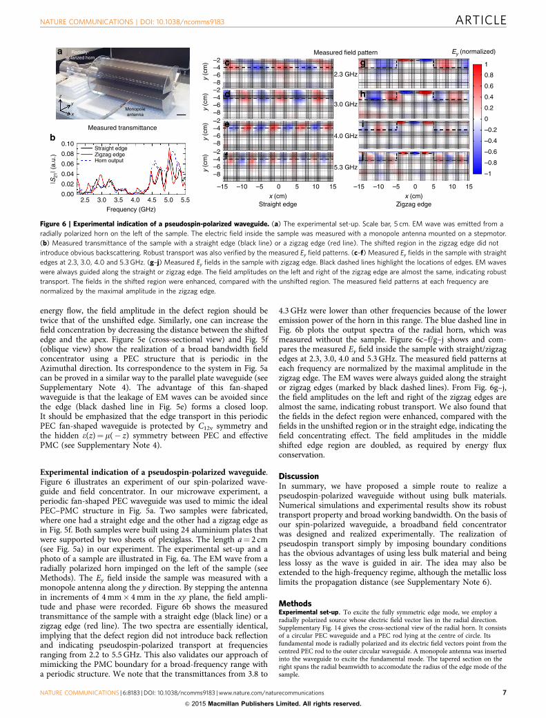
Experimental indication of a pseudospin-polarized waveguide.Figure 6 illustrates an experiment of our spin-polarized wave-guide and field concentrator. In our microwave experiment, aperiodic fan-shaped PEC waveguide was used to mimic the idealPEC–PMC structure in Fig. 5a. Two samples were fabricated,where one had a straight edge and the other had a zigzag edge asin Fig. 5f. Both samples were built using 24 aluminium plates thatwere supported by two sheets of plexiglass. The length a¼ 2 cm(see Fig. 5a) in our experiment. The experimental set-up and aphoto of a sample are illustrated in Fig. 6a. The EM wave from aradially polarized horn impinged on the left of the sample (seeMethods). The Ey field inside the sample was measured with amonopole antenna along the y direction. By stepping the antennain increments of 4 mm� 4 mm in the xy plane, the field ampli-tude and phase were recorded. Figure 6b shows the measuredtransmittance of the sample with a straight edge (black line) or azigzag edge (red line). The two spectra are essentially identical,implying that the defect region did not introduce back reflectionand indicating pseudospin-polarized transport at frequenciesranging from 2.2 to 5.5 GHz. This also validates our approach ofmimicking the PMC boundary for a broad-frequency range witha periodic structure. We note that the transmittances from 3.8 to
4.3 GHz were lower than other frequencies because of the loweremission power of the horn in this range. The blue dashed line inFig. 6b plots the output spectra of the radial horn, which wasmeasured without the sample. Figure 6c–f/g–j shows and com-pares the measured Ey field inside the sample with straight/zigzagedges at 2.3, 3.0, 4.0 and 5.3 GHz. The measured field patterns ateach frequency are normalized by the maximal amplitude in thezigzag edge. The EM waves were always guided along the straightor zigzag edges (marked by black dashed lines). From Fig. 6g–j,the field amplitudes on the left and right of the zigzag edges arealmost the same, indicating robust transport. We also found thatthe fields in the defect region were enhanced, compared with thefields in the unshifted region or in the straight edge, indicating thefield concentrating effect. The field amplitudes in the middleshifted edge region are doubled, as required by energy fluxconservation.
DiscussionIn summary, we have proposed a simple route to realize apseudospin-polarized waveguide without using bulk materials.Numerical simulations and experimental results show its robusttransport property and broad working bandwidth. On the basis ofour spin-polarized waveguide, a broadband field concentratorwas designed and realized experimentally. The realization ofpseudospin transport simply by imposing boundary conditionshas the obvious advantages of using less bulk material and beingless lossy as the wave is guided in air. The idea may also beextended to the high-frequency regime, although the metallic losslimits the propagation distance (see Supplementary Note 6).
MethodsExperimental set-up. To excite the fully symmetric edge mode, we employ aradially polarized source whose electric field vector lies in the radial direction.Supplementary Fig. 14 gives the cross-sectional view of the radial horn. It consistsof a circular PEC waveguide and a PEC rod lying at the centre of circle. Itsfundamental mode is radially polarized and its electric field vectors point from thecentred PEC rod to the outer circular waveguide. A monopole antenna was insertedinto the waveguide to excite the fundamental mode. The tapered section on theright spans the radial beamwidth to accomodate the radius of the edge mode of thesample.
–2–4–6–8–2–4–6–8–2–4–6–8–2–4–6–8
0.10
0.08
0.06
0.04
0.02
0.002.5 3.0 3.5 4.0 4.5 5.0 5.5
Radially-polarized horn
Monopoleantenna
z
y
x
Measured transmittance
Straight edgeZigzag edge
Zigzag edge
Horn output
Frequency (GHz)
|S21
| (a.
u.)
–15 –10 –5 0 5 10 15 –15 –10 –5 0 5 10 15
Straight edgex (cm) x (cm)
y (c
m)
y (c
m)
y (c
m)
y (c
m) 1
0.8
0.6
0.4
0.2
–0.2
–0.4
–0.6
–0.8
–1
0
2.3 GHz
3.0 GHz
4.0 GHz
5.3 GHz
Measured field pattern Ey (normalized)a
b
c g
h
i
j
d
e
f
Figure 6 | Experimental indication of a pseudospin-polarized waveguide. (a) The experimental set-up. Scale bar, 5 cm. EM wave was emitted from a
radially polarized horn on the left of the sample. The electric field inside the sample was measured with a monopole antenna mounted on a stepmotor.
(b) Measured transmittance of the sample with a straight edge (black line) or a zigzag edge (red line). The shifted region in the zigzag edge did not
introduce obvious backscattering. Robust transport was also verified by the measured Ey field patterns. (c–f) Measured Ey fields in the sample with straight
edges at 2.3, 3.0, 4.0 and 5.3 GHz. (g–j) Measured Ey fields in the sample with zigzag edge. Black dashed lines highlight the locations of edges. EM waves
were always guided along the straight or zigzag edge. The field amplitudes on the left and right of the zigzag edge are almost the same, indicating robust
transport. The fields in the shifted region were enhanced, compared with the unshifted region. The measured field patterns at each frequency are
normalized by the maximal amplitude in the zigzag edge.
NATURE COMMUNICATIONS | DOI: 10.1038/ncomms9183 ARTICLE
NATURE COMMUNICATIONS | 6:8183 | DOI: 10.1038/ncomms9183 | www.nature.com/naturecommunications 7
& 2015 Macmillan Publishers Limited. All rights reserved.

References1. Espinola, R. L., Izuhara, T., Tsai, M.-C., Osgood, R. M. & Dotsch, H.
Magneto-optical nonreciprocal phase shift in garnet/silicon-on-insulatorwaveguides. Opt. Lett. 9, 941–943 (2004).
2. Zaman, T. R., Guo, X. & Ram, R. J. Faraday rotation in an InP waveguide. Appl.Phys. Lett. 90, 023514 (2007).
3. Bi, L. et al. On-chip optical isolation in monolithically integrated non-reciprocal optical resonators. Nat. Photon 5, 758–762 (2011).
4. Gallo, K., Assanto, G., Parameswaran, K. R. & Fejer, M. M. All-optical diode ina periodically poled lithium niobate waveguide. Appl. Phys. Lett. 79, 314–316(2001).
5. Soljacic, M., Luo, C., Joannopoulos, J. D. & Fan, S. Nonlinear photonicmicrodevices for optical integration. Opt. Lett. 28, 637–639 (2003).
6. Fan, L. et al. An all-silicon passive optical diode. Science 335, 447–450 (2012).7. Yu, Z. & Fan, S. Complete optical isolation created by indirect interband
photonic transitions. Nat. Photon 3, 91–94 (2009).8. Kang, M. S., Butsch, A. & Russell, P. St J. Reconfigurable light-driven
opto-acoustic isolators in photonic crystal fibre. Nat. Photon 5, 549–553 (2011).9. Lira, H., Yu, Z., Fan, S. & Lipson, M. Electrically driven nonreciprocity induced
by interband photonic transition on a silicon chip. Phys. Rev. Lett. 109, 033901(2012).
10. Haldane, F. D. M. & Raghu, S. Possible realization of directional opticalwaveguides in photonic crystals with broken time-reversal symmetry. Phys. Rev.Lett. 100, 013904 (2008).
11. Wang, Z., Chong, Y., Joannopoulos, J. D. & Soljacic, M. Observation ofunidirectional backscattering-immune topological electromagnetic states.Nature 461, 772–776 (2009).
12. Ao, X., Lin, Z. & Chan, C. T. One-way edge mode in a magneto-opticalhoneycomb photonic crystal. Phys. Rev. B 80, 033105 (2009).
13. Fang, K., Yu, Z. & Fan, S. Realizing effective magnetic field for photonsby controlling the phase of dynamic modulation. Nat. Photon 6, 782–787(2012).
14. Haldane, F. D. M. Model for a quantum Hall effect without Landau levels:condensed-matter realization of the ‘‘parity anomaly’’. Phys. Rev. Lett. 61,2015–2018 (1988).
15. Jungwirth, T., Niu, Q. & MacDonald, A. H. Anomalous Hall effect inferromagnetic semiconductors. Phys. Rev. Lett. 88, 207208 (2002).
16. Kane, C. L. & Mele, E. J. Quantum spin Hall effect in graphene. Phys. Rev. Lett.95, 226801 (2005).
17. Abanin, D. A., Lee, P. A. & Levitov, L. S. Spin-filtered edge states and quantumHall effect in graphene. Phys. Rev. Lett. 96, 176803 (2006).
18. Murakami, S. Quantum spin Hall effect and enhanced magnetic response byspin-orbit coupling. Phys. Rev. Lett. 97, 236805 (2006).
19. Moore, J. E. The birth of topological insulators. Nature 464, 194–198 (2010).20. Xia, Y. et al. Observation of a large-gap topological-insulator class with a single
Dirac cone on the surface. Nat. Phys. 5, 398–402 (2009).21. Konig, M. et al. Quantum spin Hall insulator state in HgTe quantum wells.
Science 318, 766–770 (2007).22. Novoselov, K. S. et al. Room-temperature quantum Hall effect in graphene.
Science 315, 1379 (2007).23. Hafezi, M., Demler, E. A., Lukin, M. D. & Taylor, J. M. Robust optical delay
lines with topological protection. Nat. Phys. 7, 907–912 (2011).24. Hafezi, M., Mittal, S., Fan, J., Migdall, A. & Taylor, J. M. Imaging topological
edge states in silicon photonics. Nat. Photon 7, 1001–1005 (2013).25. Liang, G. Q. & Chong, Y. D. Optical resonator analog of a two-dimensional
topological insulator. Phys. Rev. Lett. 110, 203904 (2013).26. Khanikaev, A. B. et al. Photonic topological insulators. Nat. Mater. 12, 233–239
(2012).27. Chen, W.-J. et al. Experimental realization of photonic topological insulator in
a uniaxial metacrystal waveguide. Nat. Commun. 5, 5782 (2014).
28. Lu, L., Joannopoulos, J. D. & Soljacic, M. Topological photonics. Nat. Photon 8,821–829 (2014).
29. Shomroni, I. et al. All-optical routing of single photons by a one-atom switchcontrolled by a single photon. Science 345, 903–906 (2014).
30. Mitsch, R., Sayrin, C., Albrecht, B., Schneeweiss, P. & Rauschenbeutel, A.Quantum state-controlled directional spontaneous emission of photons into ananophotonic waveguide. Nat. Commun. 5, 5713 (2014).
31. Silveirinha, M. & Engheta, N. Tunneling of electromagnetic energy throughsubwavelength channels and bends using e-near-zero materials. Phys. Rev. Lett.97, 157403 (2006).
32. Edwards, B., Alu, A., Young, M. E., Silveirinha, M. & Engheta, N. Experimentalverification of epsilon-near-zero metamaterial coupling and energy squeezingusing a microwave waveguide. Phys. Rev. Lett. 100, 033903 (2008).
33. Sievenpiper, D., Zhang, L., Broas, R. F. J., Alexopolous, N. G. &Yablonovitch, E. High-impedance electromagnetic surfaces with a forbiddenfrequency band. IEEE Trans. Microwave Theory Tech. 47, 2059–2074 (1999).
34. Stockman, M. I. Nanofocusing of optical energy in tapered plasmonicwaveguides. Phys. Rev. Lett. 93, 137404 (2004).
35. Verhagen, E., Spasenovic, M., Polman, A. & Kuipers, L. Nanowire plasmonexcitation by adiabatic mode transformation. Phys. Rev. Lett. 102, 203904(2009).
36. Rahm, M. et al. Design of electromagnetic cloaks and concentrators usingform-invariant coordinate transformations of Maxwell’s equations. Photonic.Nanostruct. 6, 87–95 (2008).
37. Leonhardt, U. Optical conformal mapping. Science 312, 1777–1780 (2006).38. Pendry, J. B., Schurig, D. & Smith, D. R. Controlling electromagnetic fields.
Science 312, 1780–1782 (2006).
AcknowledgementsWe thank Dr Zhi Hong Hang for helpful discussions. This work is supported by HongKong Research Grant Council grant AOE/P-02/12. J.-W.D. is supported by the NationalNatural Science Foundation of China (11274396), Guangdong Distinguished YoungScholar and Program for New Century Excellent Talents in University.
Author contributionsW.-J.C. conceived the idea and performed the measurements. Z.-Q.Z., J.-W.D. andC.T.C. analysed the results and participated in discussions. W.-J.C. and C.T.C. co-wrotethe manuscript.
Additional informationSupplementary Information accompanies this paper at http://www.nature.com/naturecommunications
Competing financial interests: The authors declare no competing financial interests.
Reprints and permission information is available online at http://npg.nature.com/reprintsandpermissions/
How to cite this article: Chen, W.-J. et al. Symmetry-protected transport in apseudospin-polarized waveguide. Nat. Commun. 6:8183 doi: 10.1038/ncomms9183(2015).
This work is licensed under a Creative Commons Attribution 4.0International License. The images or other third party material in this
article are included in the article’s Creative Commons license, unless indicated otherwisein the credit line; if the material is not included under the Creative Commons license,users will need to obtain permission from the license holder to reproduce the material.To view a copy of this license, visit http://creativecommons.org/licenses/by/4.0/
ARTICLE NATURE COMMUNICATIONS | DOI: 10.1038/ncomms9183
8 NATURE COMMUNICATIONS | 6:8183 | DOI: 10.1038/ncomms9183 | www.nature.com/naturecommunications
& 2015 Macmillan Publishers Limited. All rights reserved.