SYLLABUS - EduOnCloudeduoncloud.com/sites/default/files/BE- Logic Design Note for CS...Logic Design....
50
Logic Design. 10CS33 SYLLABUS PART-A UNIT – 1 7 Hours Digital Principles, Digital Logic: Definitions for Digital Signals, Digital Waveforms, Digital Logic, 7400 TTL Series, TTL Parameters The Basic Gates: NOT, OR, AND, Universal Logic Gates: NOR, NAND, Positive and Negative Logic, Introduction to HDL. UNIT – 2 6 Hours Combinational Logic Circuits Sum-of-Products Method, Truth Table to Karnaugh Map, Pairs Quads, and Octets, Karnaugh Simplifications, Don’t-care Conditions, Product-of-sums Method, Product-of-sums simplifications, Simplification by Quine- McClusky Method, Hazards and Hazard Covers, HDL Implementation Models. UNIT – 3 6 Hours Data-Processing Circuits: Multiplexers, Demultiplexers, 1-of-16 Decoder, Encoders, Exclusive-or Gates, Parity Generators and Checkers, MagnitudeComparator, Programmable Array Logic, Programmable Logic Arrays, HDL Implementation of Data Processing Circuits UNIT – 4 7 Hours Clocks, Flip-Flops: Clock Waveforms, TTL Clock, Schmitt Trigger, Clocked D FLIP-FLOP, Edge-triggered D FLIP-FLOP, Edge-triggered JK FLIP-FLOP, FLIP-FLOP Timing, JK Master-slave FLIP-FLOP, Switch Contact Bounce Circuits, Various Representation of FLIP-FLOPs, Analysis of Sequential Circuits, HDL Implementation of FLIP-FLOP PART-B UNIT – 5 6 Hours Registers: Types of Registers, Serial In - Serial Out, Serial In - Parallel out, Parallel In - Serial Out, Parallel In - Parallel Out, Universal Shift Register, Applications of Shift Registers, Register Implementation in HDL UNIT – 6 7 Hours Counters: Asynchronous Counters, Decoding Gates, Synchronous Counters, Changing the Counter Modulus, decade Design Counters, Presettable Counters, Counter Design as a Synthesis problem, A Digital Clock, Counter using HDL UNIT – 7 7 Hours Design of Synchronous and Asynchronous Sequential Circuits: Design of Synchronous Sequential Circuit: Model Selection, State Transition Diagram, State Synthesis Table, Design Equations and Circuit Diagram, Implementation using Read Only Memory, Algorithmic State Machine, State Reduction Technique. Asynchronous Sequential Circuit: Analysis of Asynchronous Sequential Circuit, Problems with Asynchronous Sequential Circuits, Design of Asynchronous Sequential Circuit, FSM Implementation in HDL UNIT – 8 6 Hours D/A Conversion and A/D Conversion: Variable, Resistor Networks, Binary Ladders, D/A Converters, D/A Accuracy and Resolution, A/D Converter- Simultaneous Conversion, A/D Converter-Counter Method, Continuous A/D Conversion, A/D Techniques, Dual-slope A/D Conversion, A/D Accuracy and Resolution Dept. of ISE, SJBIT 1
Transcript of SYLLABUS - EduOnCloudeduoncloud.com/sites/default/files/BE- Logic Design Note for CS...Logic Design....

Logic Design. 10CS33
SYLLABUS
PART-A
UNIT – 1 7 Hours
Digital Principles, Digital Logic: Definitions for Digital Signals, Digital Waveforms, Digital Logic, 7400 TTL
Series, TTL Parameters The Basic Gates: NOT, OR, AND, Universal Logic Gates: NOR, NAND, Positive and
Negative Logic, Introduction to HDL.
UNIT – 2 6 Hours
Combinational Logic Circuits Sum-of-Products Method, Truth Table to Karnaugh Map, Pairs Quads, and Octets, Karnaugh Simplifications,
Don’t-care Conditions, Product-of-sums Method, Product-of-sums simplifications, Simplification by Quine-
McClusky Method, Hazards and Hazard Covers, HDL Implementation Models.
UNIT – 3 6 Hours Data-Processing Circuits: Multiplexers, Demultiplexers, 1-of-16 Decoder, Encoders, Exclusive-or Gates,
Parity Generators and Checkers, MagnitudeComparator, Programmable Array Logic, Programmable Logic
Arrays, HDL
Implementation of Data Processing Circuits
UNIT – 4 7 Hours
Clocks, Flip-Flops: Clock Waveforms, TTL Clock, Schmitt Trigger, Clocked D FLIP-FLOP, Edge-triggered D
FLIP-FLOP, Edge-triggered JK FLIP-FLOP, FLIP-FLOP Timing, JK Master-slave FLIP-FLOP, Switch Contact
Bounce Circuits, Various Representation of FLIP-FLOPs, Analysis of Sequential Circuits, HDL Implementation
of FLIP-FLOP
PART-B
UNIT – 5 6 Hours
Registers: Types of Registers, Serial In - Serial Out, Serial In - Parallel out, Parallel In - Serial Out, Parallel In -
Parallel Out, Universal Shift Register, Applications of Shift Registers, Register Implementation in HDL
UNIT – 6 7 Hours
Counters: Asynchronous Counters, Decoding Gates, Synchronous Counters, Changing the Counter Modulus,
decade
Design
Counters, Presettable Counters, Counter Design as a Synthesis problem, A Digital Clock, Counter
using HDL
UNIT – 7 7 Hours
Design of Synchronous and Asynchronous Sequential Circuits: Design of Synchronous Sequential Circuit:
Model Selection, State Transition Diagram, State Synthesis Table, Design Equations and Circuit Diagram,
Implementation using Read Only Memory, Algorithmic State Machine, State Reduction Technique.
Asynchronous Sequential Circuit: Analysis of Asynchronous Sequential Circuit, Problems with Asynchronous
Sequential Circuits, Design of Asynchronous Sequential Circuit, FSM Implementation in HDL
UNIT – 8 6 Hours
D/A Conversion and A/D Conversion: Variable, Resistor Networks, Binary Ladders, D/A Converters, D/A
Accuracy and Resolution, A/D Converter- Simultaneous Conversion, A/D Converter-Counter Method,
Continuous A/D Conversion, A/D Techniques, Dual-slope A/D Conversion, A/D Accuracy and Resolution
Dept. of ISE, SJBIT 1

Logic Design. 10CS33
Text Book:
1. Donald P Leach, Albert Paul Malvino & Goutam Saha: Digital Principles and Applications, 7th Edition, Tata
McGraw Hill, 2010.
Reference Books: 1. Stephen Brown, Zvonko Vranesic: Fundamentals of Digital Logic Design with VHDL, 2nd Edition, Tata
McGraw Hill, 2005.
2. R D Sudhaker Samuel: Illustrative Approach to Logic Design, Sanguine-Pearson, 2010.
3. Charles H. Roth: Fundamentals of Logic Design, Jr., 5th Edition, Cengage Learning, 2004.
4. Ronald J. Tocci, Neal S. Widmer, Gregory L. Moss: Digital Systems Principles and Applications, 10th
Edition, Pearson Education, 2007.
Dept. of ISE, SJBIT 2

Logic Design. 10CS33
TABLE OF CONTENTS
Unit-1 : Digital Principles, Digital Logic Page No.
1.1 Definitions for Digital Signals 6
1.2 Digital Waveforms 7
1.3 Digital Logic 7400 TTL Series, TTL Parameters The Basic 7
1.4 Gates: NOT, OR, AND, 10
1.5 Universal Logic Gates: NOR, NAND 12
1.6 Positive and Negative Logic 13
1.7 Introduction to HDL. 15
Unit-2 : Combinational Logic Circuits
2.1 Sum-of-Products Method 17
2.2 Truth Table to Karnaugh Map 18
2.3 Pairs Quads, and Octets 20
2.4 Karnaugh Simplifications, Don’t-care Conditions 21
2.5 Product-of-sums 21
2.6 Method, Product-of-sums simplifications 23
2.7 Simplification by Quine-McClusky 25
2.9 HDL Implementation Models. 27
Unit-3 :Data-Processing Circuits
3.1 Multiplexers 29
3.2 Demultiplexers 30
3.3 1-of-16 Decoder 31
3.4 Priority Encoders 31
3.5 Exclusive-or Gates 33
3.6 Parity Generators and Checkers 34
3.7 Magnitude Comparator 35
3.8 Programmable Array Logic 36
3.9 Programmable Logic Arrays, HDL 38
3.10 Implementation of Data Processing Circuits 40
Dept. of ISE, SJBIT 3
Logic Design. 10CS33
Unit-4 : Clocks, Flip Flops
4.1 Clock Waveforms & TTL Clock 41
4.2 Schmitt Trigger 41
4.3 Combinational logic circuit 42
4.4 Latches 43
4.5 Application of SR Latches 43
4.6 FLIP-FLOP Timing 44
4.7 JK Master-slave FLIP-FLOP 44
4.8 Switch Contact Bounce Circuits 45
4.9 Various Representations of FLIP-FLOPs 46
4.10 Analysis of Sequential Circuits 47
4.11 HDL Implementation of FLIP-FLOP 49
Unit-5 : Registers
5.1 Types of Registers 50
5.2 Serial In - Serial Out 50
5.3 Serial In - Parallel out 50
5.4 Parallel In - Serial Out 50
5.5 Parallel In - Parallel Out 50
5.6 Universal Shift Register 51
5.7 Applications of Shift Registers 52
5.8 Register Implementation in HDL 52
Unit-6 : Counters
6.1 Counters 53
6.2 4-bit Binary Counter 53
6.3 Synchronous Counters 54
6.4 Changing the Counter Modulus 54
6.5 Decade Counters, Presettable Counters 54
6.6 Johnson Counter 55
Logic Design. 10CS33
Dept. of ISE, SJBIT 4
6.8 Counter Design using HDL 57
Unit-7: Design of Synchronous and Asynchronous Sequential Circuits
7.1 Model Selection 58
7.2 Design Equations and Circuit Diagram, 57
7.3 Implementation using Read Only Memory 58
7.4 Algorithmic State Machine, State 59
7.5 Reduction Technique. 60
7.6 Asynchronous Sequential Circuit: Analysis of Asynchronous Sequential Circuit
63
7.7 Problems with Asynchronous Sequential Circuits 64
7.8 Design of Asynchronous Sequential Circuit 65
7.9 FSM Implementation in HDL 69
Unit-8: D/A Conversion and A/D Conversion
8.1 Variable & Resistor Network 74
8.2 D/A Converters 75
8.3 D/A Accuracy and Resolution 75
8.4 A/D Converter- Simultaneous Conversion 76
8.5 Closed Loop Frequency Response 77
8.6 Conversion, A/D Type 79
8.7 Dual-slope A/D Conversion 79
8.8 A/D Accuracy and Resolution 80
Dept. of ISE, SJBIT 5

Dept. of ISE, SJBIT 6
Unit-1 : Digital Principles, Digital Logic
1.1 Definitions of Analog vs Digital signals
An Analog signal is any continuous signal for which the time varying feature (variable) of the signal
is a representation of some other time varying quantity, i.e., analogous to another time varying signal.
It differs from a digital signal in terms of small fluctuations in the signal which are meaningful.
A digital signal uses discrete (discontinuous) values. By contrast, non-digital (or analog) systems use
a continuous range of values to represent information. Although digital representations are discrete,
the information represented can be either discrete, such as numbers or letters, or continuous, such as
sounds, images, and other measurements of continuous systems.
Comparison chart
Analog
Digital
Technology:
Analog technology records waveforms as
they are.
Converts analog waveforms into set of
numbers and records them. The numbers
are converted into voltage stream for
representation.
Representation: Uses continuous range of values to represent information.
Uses discrete or discontinuous values to
represent information.
Uses:
Signal:
Can be used in various computing
platforms and under operating systems
like Linux, Unix, Mac OS and Windows.
Analog signal is a continuous signal which
transmits information as a response to
changes in physical phenomenon.
Computing and electronics
Digital signals are discrete time signals
generated by digital modulation.
Clocks:
Computer:
Analog clocks indicate time using angles.
Analog computer uses changeable
continuous physical phenomena such as
electrical, mechanical, hydraulic
quantities so as to solve a problem.
Digital clocks use numeric representation
to indicate time.
Digital computers represent changing
quantities incrementally as and when
their values change.

Dept. of ISE, SJBIT 7
1.2 Waveforms in digital systems
In computer architecture and other digital systems, a waveform that switches between two voltage
levels representing the two states of a Boolean value (0 and 1) is referred to as a digital signal, even
though it is an analog voltage waveform, since it is interpreted in terms of only two levels.
The clock signal is a special digital signal that is used to synchronize digital circuits. The image
shown can be considered the waveform of a clock signal. Logic changes are triggered either by the
rising edge or the falling edge.
The given diagram is an example of the practical pulse and therefore we have introduced two new
terms that are:
• Rising edge: the transition from a low voltage (level 1 in the diagram) to a high voltage (level
2).
• Falling edge: the transition from a high voltage to a low one.
•
1.3 TTL Series
Normally Binary Logic Values are are defined as either Logic ‘1’or Logic ‘0’ depending on the level
of the output voltage. Another additional (intermediate value ) is the ‘Undefined value’. Logic levels
can either be Positive logic or Negative Logic. For eg:
In TTL Logic Levels (positive logic) logic high or Logic 1 is between 2.4 V≤ VH ≤ 5V. Logic ‘0’ or
low logic is between 0V≤ VL ≤ 0.4 V and the Undefined value is between 0.4 V <undefined< 2.4 V
Logic families are classified based on either the devices used ,example: diodes ,transistors etc. or the
structure of Digital Circuits , example: ECL ,Wired logic etc.
The following are the examples of logic families based on the devices used and their structure,
• DTL
• RTL
• TTL
• ECL
:Diode Transistor Logic
:Resistor Transistor Logic
:Transistor Transistor Logic
:Emitter Coupled Logic
• CMOS :Complementary MOSFET Logic
The various logic families differ in the current driving capabilities,Logic Levels, propagation delays
and a few other other parameters. The Comparison of TTL and CMOS is clearly illustrated in the
following table as an example of differences in the logic families:

Dept. of ISE, SJBIT 8
TTL CMOS
• Faster
• Stronger drive
capability
• Low power consumption
• Simpler to make
• Greater packing density
• Better noise immunity
Integration Levels:
The devices greatly differ in the density of fabrication ie the levels of integration used.Depending on
the number of transistors/diodes/gates used in the chip they are broadly classified as :
• SSI -small scale integration
• MSI -medium scale integration
• LSI -large scale integration
• VLSI -very large scale integration
• ULSI -ultra large scale integration
• GSI -giant scale integration
Levels of integration Transistors/package Gates/chip Applications
SSI 1-100 <12 Logic gates Op-amps
MSI 100-1000 12-99 Registers Filters
LSI 1000-10000 1000 8 bit processor, A/D converter
VLSI 10k gates/chip 16,32 bit processor
256KB memory
DS processor
ULSI 100k gates/chip 64 bit processor
8 MB memory
Image processor

Dept. of ISE, SJBIT 9
GSI 1M gates/chip 64 MB memory
multiprocessor
Speed of Operation:
As signals propagate through the various gates there is a finite time required for the signal change
to occur, eg the time required for the input high of a n inverter to change to logic low at the
output. This implies that there is a limitation on the no of times the output can change or the speed
of operation of the gate. The parameters of importance for the speed of operation are :
• tLH- low to high rise time (tr) : it is defined as the time interval for the signal to rise between
10% to 90% of Vdd
• tHL- high to low time or fall time (tf): it is defined as the time for signal to fall from 90%Vdd
to 10%Vdd
•
The switching is fast with tmin=thl+tlh
Therefore maximum switching freq is achieved when fmax=1/tmin
The switching speed is limited due to the effect of capacitance
ground etc.
at the base emmiter /collector and
For eg: if thl =0.5 nsec, tlh=1.0 nsec
Then tmin =1.5 nsec And fmax=1/ tmin=666.67Mhz
Propagation delay:
It is the physical delay as the logical signal propagates through the gates. It differs depending on
whether the output transition goes from cutoff to saturation or from saturation to cut-off.
As the loads are connected to gates to realize the necessary logic operations the output signal levels
are affected. This is because there is a current flow between the gates due to which there is power
consumption. Thus
limited.
the number of circuits(similar gates) that can be connected to the gates gets
Dept. of ISE, SJBIT 10
• Fan-out of a gate is the number of gates driven by that gate i.e the maximum number of gates
(load ) that can exist without impairing the normal operation of the gate.
• Fan-in of a gate is the number of inputs that can be connected to it without impairing the
normal operation of the gate.
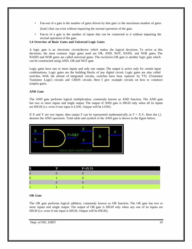
1.4 Overview of Basic Gates and Universal Logic Gates
A logic gate is an electronic circuit/device which makes the logical decisions. To arrive at this
decisions, the most common logic gates used are OR, AND, NOT, NAND, and NOR gates. The
NAND and NOR gates are called universal gates. The exclusive-OR gate is another logic gate which
can be constructed using AND, OR and NOT gate.
Logic gates have one or more inputs and only one output. The output is active only for certain input
combinations. Logic gates are the building blocks of any digital circuit. Logic gates are also called
switches. With the advent of integrated circuits, switches have been replaced by TTL (Transistor
Transistor Logic) circuits and CMOS circuits. Here I give example circuits on how to construct
simples gates.
AND Gate
The AND gate performs logical multiplication, commonly known as AND function. The AND gate
has two or more inputs and single output. The output of AND gate is HIGH only when all its inputs
are HIGH (i.e. even if one input is LOW, Output will be LOW).
If X and Y are two inputs, then output F can be represented mathematically as F = X.Y, Here dot (.)
denotes the AND operation. Truth table and symbol of the AND gate is shown in the figure below.
X Y F=(X.Y)
0 0 0
0 1 0
1 0 0
1 1 1
OR Gate
The OR gate performs logical addition, commonly known as OR function. The OR gate has two or
more inputs and single output. The output of OR gate is HIGH only when any one of its inputs are
HIGH (i.e. even if one input is HIGH, Output will be HIGH).

Dept. of ISE, SJBIT 11
If X and Y are two inputs, then output F can be represented mathematically as F = X+Y. Here plus
sign (+) denotes the
below.
OR operation. Truth table and symbol of the OR gate is shown in the figure
YF=(X+Y)
0 0 0
0 1 1
1 0 1
1 1 1
NOT Gate
The NOT gate performs the basic logical function called inversion or complementation. NOT gate is
also called inverter. The purpose of this gate is to convert one logic level into the opposite logic level.
It has one input and one output. When a HIGH level is applied to an inverter, a LOW level appears on
its output and vice versa.
If X is the input, then output F can be represented mathematically as F = X', Here apostrophe (')
denotes the NOT (inversion) operation. There are a couple of other ways to represent inversion, F=
!X, here ! represents inversion. Truth table and NOT gate symbol is shown in the figure below.
X Y=X'
0 1
1 0
NAND Gate
NAND gate is a cascade of AND gate and NOT gate, as shown in the figure below. It has two or more
inputs and only one output. The output of NAND gate is HIGH when any one of its input is LOW (i.e.
even if one input is LOW, Output will be HIGH).

Dept. of ISE, SJBIT 12
X Y F=(X.Y)'
0 0 1
0 1 1
1 0 1
1 1 0
NOR Gate
NOR gate is a cascade of OR gate and NOT gate, as shown in the figure below. It has two or more
inputs and only one output. The output of NOR gate is HIGH when any all its inputs are LOW (i.e.
even if one input is HIGH, output will be LOW).
X Y F=(X+Y)'
0 0 1
0 1 0
1 0 0
1 1 0
XOR Gate
An Exclusive-OR (XOR) gate is gate with two or three or more inputs and one output. The output of a
two-input XOR gate assumes a HIGH state if one and only one input assumes a HIGH state. This is
equivalent to saying that the output is HIGH if either input X or input Y is HIGH exclusively, and
LOW when both are 1 or 0 simultaneously.
If X and Y are two inputs, then output F can be represented mathematically as F = X Y, Here
denotes the XOR operation. X Y and is equivalent to X.Y' + X'.Y. Truth table and symbol of the
XOR gate is shown in the figure below.

Dept. of ISE, SJBIT 13
X Y F=(X Y)
0 0 0
0 1 1
1 0 1
1 1 0
XNOR Gate
An Exclusive-NOR (XNOR) gate is gate with two or three or more inputs and one output. The output
of a two-input XNOR gate assumes a HIGH state if all the inputs assumes same state. This is
equivalent to saying that the output is HIGH if both input X and input Y is HIGH exclusively or same
as input X and input Y is LOW exclusively, and LOW when both are not same.
If X and Y are two inputs, then output F can be represented mathematically as F = X Y, Here
denotes the XNOR operation. X Y and is equivalent to X.Y + X'.Y'. Truth table and symbol of
the XNOR gate is shown in the figure below.
X Y F=(X Y)'
0 0 1
0 1 0
1 0 0
1 1 1
1.6 Boolean Laws and Theorems
A. Axioms
Consider a set S = { 0. 1} Consider two binary operations, + and . , and one unary operation, -- , that act
on these elements. [S, ., +, --, 0, 1] is called a switching algebra that satisfies the following axioms S.
B. Closure
If X
If X
S and Y
S and Y
S then X.Y S
S then X+Y
S
C. Identity
an identity 0 for + such that X + 0 = X
an identity 1 for . such that X . 1 = X
D. Commutative Laws
X + Y = Y + X
X Y = Y X
E. Distributive Laws
X.(Y + Z ) = X.Y + X.Z
X + Y.Z = (X + Y) . (X + Z)
Idempotent Law
X + X = X
X X = X
DeMorgan's Law
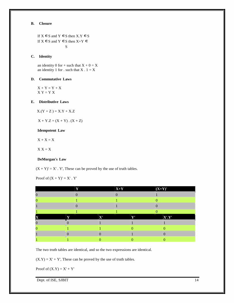
(X + Y)' = X' . Y', These can be proved by the use of truth tables.
Proof of (X + Y)' = X' . Y'
Y X+Y (X+Y)'
0 0 0 1
0 1 1 0
1 0 1 0
1 1 1 0
X Y X' Y' X'.Y'
0 0 1 1 1
0 1 1 0 0
1 0 0 1 0
1 1 0 0 0
The two truth tables are identical, and so the two expressions are identical.
(X.Y) = X' + Y', These can be proved by the use of truth tables.
Proof of (X.Y) = X' + Y'
Dept. of ISE, SJBIT 14

Logic Design. 10CS33
X Y X.Y (X.Y)'
0 0 0 1
0 1 0 1
1 0 0 1
1 1 1 0
X Y X' Y' X'+Y'
0 0 1 1 1
0 1 1 0 1
1 0 0 1 1
1 1 0 0 0
1.7 Introduction to HDL: Hardware Description Language
HDL is a language that describes the hardware of digital systems in a textual form. It resembles a
programming language, but is specifically oriented to describing hardware structures and behaviors.
The main difference with the traditional programming languages is HDL’s representation of extensive
parallel operations whereas traditional ones represents mostly serial operations. HDL can be used to
represent logic diagrams, Boolean expressions, and other more complex digital circuits
There are two standard HDL’s that are supported by IEEE.
VHDL (Very-High-Speed Integrated Circuits Hardware Description Language) -
Sometimes referred to as VHSIC HDL, this was developed from an initiative by US.
Dept. of Defense.
Verilog HDL – developed by Cadence Data systems and later transferred to a
consortium called Open Verilog International (OVI).
Verilog: Verilog HDL has a syntax that describes precisely the legal constructs that can be used in
the language.
It uses about 100 keywords pre-defined, lowercase, identifiers that define the language
constructs.
Example of keywords: module, endmodule, input, output wire, and, or, not , etc.,
Any text between two slashes (//) and the end of line is interpreted as a comment.
Blank spaces are ignored and names are case sensitive.
A module is the building block in Verilog. It is declared by the keyword module and is always
terminated by the keyword endmodule.Each statement is terminated with a semicolon, but there is
no semi-colon after endmodule.
HDL Example
module smpl_circuit(A,B,C,x,y);
input A,B,C;
output x,y;
wire e;
and
Dept. of ISE, SJBIT
g1(e,A,B);
15

Logic Design. 10CS33
Unit-2 : Combinational Logic Circuits
DeMorgans Laws are applicable for any number of variables.
Boundedness Law
X + 1 = 1
X . 0 = 0
Absorption Law
X + (X . Y) = X
X . (X + Y ) = X
Elimination Law
X + (X' . Y) = X + Y
X.(X' + Y) = X.Y
Unique Complement theorem
If X + Y = 1 and X.Y = 0 then X = Y'
Involution theorem
X'' = X
0' = 1
Associative Properties
X + (Y + Z) = (X + Y) + Z
X . ( Y . Z ) = ( X . Y ) . Z
PRINCIPLE OF DUALITY
One can transform the given expression by interchanging the operation (+) and (•) as well as
the identity elements 0 and 1 . Then the expression will be referred as dual of each other.
This is known as the principle of duality.
Dept. of ISE, SJBIT 16

Dept. of ISE, SJBIT 17
Example x + x = 1 then the dual expression is
x • x = 0
A procedure which will be used to write Boolean expressions form truth table is known as
canonical formula. The canonical formulas are of two types
1. Minterm canonical formulas
2. Maxterm canonical formulas
2.1 Sum-of-Products Method
MINTERM CANONICAL FORMULAS
Minterms are product of terms which represents the functional values of the variables appear
either in complemented or un complemented form.
Ex: f(x,y,z) = x y z + x y z + x y z
The Boolean expression whichis represented above is also known as SOP or disjunctive
formula. The truth table is
x y z f
0 0 0 0
0 0 1 1
0 1 0 0
0 1 1 1
1 0 0 1
1 0 1 0
1 1 0 0
1 1 1 0
m- NOTATION
To simplify the writing of a minterm in canonical formula for a function is performed using
the symbol mi. Where i stands for the row number for which the function evaluates to 1.
The m-notation for 3- variable an function Boolean function
f(x,y,z) = x y z + x y z + x y z is written as
f(x,y,z) = m1+ m3 + m4 or
f(x,y,z) = ∑m(1,3,4)
A three
variable m- notation
truth
variable
x y z Decimal
designator of row
Minterm m-notation

Dept. of ISE, SJBIT 18
0 0 0 0 x y z m0
0 0 1 1 x y z m1
0 1 0 2 x y z m2
0 1 1 3 x y z m3
1 0 0 4 x y z m4
1 0 1 5 x y z m5
1 1 0 6 x y z m6
1 1 1 7 x y z m7
MAXTERM CANONICAL FORM
Maxterm are sum terms where the variable appear once either in complement or un-
complement forms and these terms corresponds to a functional value representing 0.
Ex. f(x,y,z) = ( x+ y+ z ) ( x+ y+z ) ( x + y + z )
= ∏M( 0, 2, 5)
= M0, M2, M5
2.2 KARNAUGH MAPS ( K- MAP)
A method for graphically determining implicants and implicates of a Boolean
function was developed by Veitch and modified by Karnaugh . The method involves a
diagrammatic
map.
representation of a Boolean algebra. This graphic representation is called
It is seen that the truth table can be used to represent complete function of n-variables.
Since each variable can have value of 0 or 1. The truth table has 2n rows. Each rows
of the truth table consist of two parts (1) an n-tuple which corresponds to an assignment
to the n-variables and (2) a functional value.
A Karnaugh map (K-map) is a geometrical configuration of 2n cells such
that each of the n-tuples corresponds to a row of a truth table uniquely locates a
cell on the map. The functional values assigned to the n-tuples are placed as
entries in the cells, i.e. 0 or 1 are placed in the associated cell.
An significant about the construction of K-map is the arrangement of the cells. Two
cells are physically adjacent within the configuration if and only if their respective n-
tuples differ in exactly by one element. So that the Boolean law x+x=1 cab be applied
to adjacent cells. Ex. Two 3- tuples (0,1,1) and (0,1,0) are physically a djacent since these
tuples vary by one element.
One
variable : One
variable
needs a
map of 21= 2 cells map
as shown
below
x f(x)
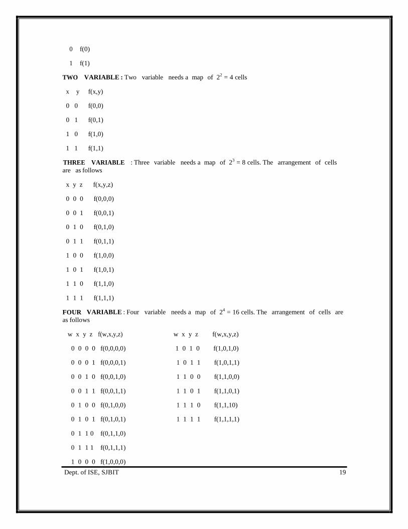
Dept. of ISE, SJBIT 19
0 f(0)
1 f(1)
TWO
VARIABLE : Two
variable
needs a map of 22
= 4 cells
x y f(x,y)
0 0 f(0,0)
0 1 f(0,1)
1 0 f(1,0)
1 1
THREE
f(1,1)
VARIABLE
: Three
variable
needs a map
of 23
= 8 cells. The
arrangement
of cells
are as follows
x y z f(x,y,z)
0 0 0 f(0,0,0)
0 0 1 f(0,0,1)
0 1 0 f(0,1,0)
0 1 1 f(0,1,1)
1 0 0 f(1,0,0)
1 0 1 f(1,0,1)
1 1 0 f(1,1,0)
1 1 1
FOUR
f(1,1,1)
VARIABLE : Four
variable
needs a
map
of 24
= 16 cells. The
arrangement
of cells
are
as follows
w x y z f(w,x,y,z) w x y z f(w,x,y,z)
0 0 0 0 f(0,0,0,0) 1 0 1 0 f(1,0,1,0)
0 0 0 1 f(0,0,0,1) 1 0 1 1 f(1,0,1,1)
0 0 1 0 f(0,0,1,0) 1 1 0 0 f(1,1,0,0)
0 0 1 1 f(0,0,1,1) 1 1 0 1 f(1,1,0,1)
0 1 0 0 f(0,1,0,0) 1 1 1 0 f(1,1,10)
0 1 0 1 f(0,1,0,1) 1 1 1 1 f(1,1,1,1)
0 1 1 0 f(0,1,1,0)
0 1 1 1 f(0,1,1,1)
1 0 0 0 f(1,0,0,0)

Dept. of ISE, SJBIT 20
1 0 0 1 f(1,0,0,1)
Four variable K-map.
0000 0001 0011 0010
0100 0101 0111 1010
1100 1101 1111 1110
1000 1001 1011 1010
Ex. Obtain the minterm canonical formula of the three variable problem given below
f(x, y,z) = x y z+ x y z + x y z + x y z
f(x,y,z) = ∑m(0,2,4,5)
00 01 11 11
1
0
0
1
1
1
0
0
Ex. Express the minterm canonical formula of the four variable K-map given below
yz
00 01 11 10
wx 1 1 0 1
1 1 0 0

Dept. of ISE, SJBIT 21
0 0 0 0
1 0 0 1
f(w,x,y,z) = w x y z + w x y z + w x y z + w x y z + w x y z + w x y z
f(w,x,y,z) = ∑ m(0, 1, 2, 4, 5,
Ex. Obtain the max term canonical formula
(POS) of the three variable problem stated above
f(x,y,z) = ( x + y +z)( x + y +z)(x + y +z)
(x + y +z)
f(x,y,z) = ΠM(1,3,6,7)
Ex Obtain the max term canonical formula
(POS) of the four variable problem stated above
f(w,x,y,z) = (w + x + y + z) (w + x + y + z) (w + x + y + z)
(w + x + y + z) (w + x + y + z) (w + x + y + z)
(w + x + y + z) (w + x + y + z) (w + x + y + z)
f(w,x,y,z) = ΠM(3,6,7,9,11,12,13,14,15)
2.3 PRODUCT AND SUM TERM REPRESENTATION OF K –MAP
1.The importance of K-map lies in the fact that it is possible to determine the implicants
and implicates of a function from the pattern of 0’s and 1’s appearing in the map. The cell
of a K-map has entry of 1’s is refereed as 1-cell and that of 0,s is referred as 0-cell.
2. The construction of an n-variable map is such that any set of 1-cells or 0-cells which
form a 2ax2
b rectangular grouping describing a product or sum term with n-a-b variables , where a
and b are non-negative no.s
3. The rectangular grouping of these dimensions referred as Subcubes. The subcubes must
be the power of 2 i.e. 2 a+b
equals to 1,2,4,8 etc.
4. For three variable and four variable K-map it must be remembered that the edges are also
adjacent cells or subcubes hence they will be grouped together.

22 Dept. of ISE, SJBIT
5. Given an n-variable map with a
or 0-cellscan result n-1 pair of adjacent 1-cells
group of four adjacent subcubes are variable.Where as if a
n-2 variables. Finally if we have formed than it can result
grouped may result n-3 variable eight adjacent cells are
Typical pair
of subcubes product or sum term.
Typical group
of four
adjacent subcube
Typical group of four adjacent subcubes.
1
1
1
1 1
1 1
1
1 1 1
1 1
1 1
1 1
1 1 1
1

Logic Design. 10CS33
Dept. of ISE, SJBIT 23
Typical group
of eight
adjacent
subcubes.
1 1
1 1
1 1
1 1
2.4 USING K-MAP
TO OBTAIN MINIMAL
EXPRESSION
FOR
COMPLETE
BOOLEAN FUNCTIONS :
How to obtain a minimal expression of SOP or POS of given function is discussed.
PRIME IMPLICANTS and K-MAPS :
CONCEPT OF ESSENTIAL PRIME IMPLICANT
00 01 11 10
0
0
0
1
0
0
1
1
f(x,y,z)= xy+ yz
ALGORITHM TO FIND ALL PRIME IMPLICANTS
1 1 1 1
1 1 1 1
1 1
1 1
1 1
1 1
1 1 1 1
1 1 1 1
Logic Design. 10CS33
Dept. of ISE, SJBIT 24
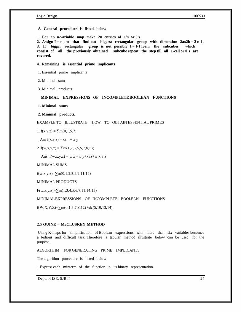
A General procedure is listed below
1. For an n-variable map make 2n entries of 1’s. or 0’s.
2. Assign I = n , so that find out biggest rectangular group with dimension 2ax2b = 2 n-1.
3. If bigger rectangular group is not possible I = I-1 form the subcubes which
consist of all
covered.
the previously obtained subcube repeat the step till all 1-cell or 0’s are
4. Remaining is essential prime implicants
1. Essential prime implicants
2. Minimal sums
3. Minimal products
MINIMAL EXPRESSIONS OF INCOMPLETE BOOLEAN FUNCTIONS
1. Minimal sums
2. Minimal products.
EXAMPLE TO ILLUSTRATE HOW TO OBTAIN ESSENTIAL PRIMES
1. f(x,y,z) = ∑m(0,1,5,7)
Ans f(x,y,z) = xz + x y
2. f(w,x,y,z) = ∑m(1,2,3,5,6,7,8,13)
Ans. f(w,x,y,z) = w z +w y+xyz+w x y z
MINIMAL SUMS
f(w,x,y,z)=∑m(0,1,2,3,5,7,11,15)
MINIMAL PRODUCTS
F(w,x,y,z)=∑m(1,3,4,5,6,7,11,14,15)
MINIMAL EXPRESSIONS OF INCOMPLETE BOOLEAN FUNCTIONS
f(W,X,Y,Z)=∑m(0,1,3,7,8,12) +dc(5,10,13,14)
2.5 QUINE – McCLUSKEY METHOD
Using K-maps for simplification of Boolean expressions with more than six variables becomes
a tedious
purpose.
and difficult task. Therefore a tabular method illustrate below can be used for the
ALGORITHM FOR GENERATING PRIME IMPLICANTS
The algorithm procedure is listed below
1. Express each minterm of the function in its binary representation.

Logic Design. 10CS33
Dept. of ISE, SJBIT 25
2. List the minterms by increasing index.
3. Separate the sets of minterms of equal index with lines.
4. Let i = 0.
5. Compare each term of index I with each term of index I+1. For each pair of terms that can
combine which has only one bit position difference.
6. Increase I by 1 and repeat step 5 . The increase of I continued until all terms are compared.
The new list containing all implicants of the function that have one less variable than those
implicants in the generating list.
7. Each section of the new list formed has terms of equal index. Steps 4,5, and 6 are repeated on
this list to form another list. Recall that two terms combine only if they have their dashes in
the same relative positions and if they differ in exactly one bit position.
8. The process terminates when no new list is formed .
9. All terms without check marks are prime implicants.
Example: Find all the prime implicants of the function
f(w,x,y,z) = ∑m(0,2,3,4,8,10,12,13,14)
Step 1: Represent each minter in its 1-0 notation
no. minterm 1-0 notation index
0 w x y z 0 0 0 0 0
2 w x y z 0 0 1 0 1
3 w x y z 0 0 1 1 2
4 w x y z 0 1 0 0 1
8 w x y z 1 0 0 0 1
10 w x y z 1 0 1 0 2
12 w x y z 1 1 0 0 2
13 w x y z 1 1 0 1 3
14 w x y z 1 1 1 0 3
Step 2: List
the
minterm in
increasing
order
of their
index.
No. w x y z index
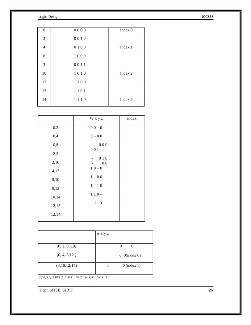
Logic Design. 10CS33
Dept. of ISE, SJBIT 26
0 0 0 0 0 Index 0
2 0 0 1 0
4 0 1 0 0 Index 1
8 1 0 0 0
3 0 0 1 1
10 1 0 1 0 Index 2
12 1 1 0 0
13 1 1 0 1
14 1 1 1 0 Index 3
W x y z index
0.2 0 0 – 0
0,4 0 – 0 0
0,8 - 0 0 0
0 0 1 – 2,3
- 0 1 0 2,10 - 1 0 0
4,12 1 0 – 0
8,10 1 – 0 0
8,12 1 – 1 0
10,14 1 1 0 –
12,13 1 1 - 0
12,14
w x y z
(0, 2, 8, 10)
(0, 4, 8,12 )
0 0
0 0(index 0)
(8,10,12,14) 1 0 (index 1)
F(w,x,y,z)=x z + y z +w z+w x y +w x z

Logic Design. 10CS33
Dept. of ISE, SJBIT 27
PETRICK’S METHOD OF DETERMINING IRREDUNDANT EXPRESSIONS
FIND THE PRIME IMPLICANTS AND IRREDUNDANT EXPRESSION
F(W,X,Y,Z)= ∑M(0,1,2,5,7,8,9,10,13,15)
A=X Y , B= X Z C= Y Z D= X Z
P = (A+B)(A+C) (B)(C+D)(D)(A+B)(A+C)(B)(C+D)(D)
P = (A +C)(BD) = ABD +BCD
F1(W,X,Y,Z)= ABD =X Y +X Z +X Z
F2(W,X,Y,Z) = BCD = X Z + Y Z +X Z
DECIMAL METHOD FOR OBTAINING PRIME IMPLICANTS
The prime implicants can be obtained for decimal number represented minterms.In this procedure
binary number are not used to find out prime implicants
f(w, x,y,z) =∑m(0,5,6,7,9,10,13,14,15)
fsop= xy +xz+xyz+wyz+w x y z
MAP ENTERED VARIABLE(MEV)
It is graphical approach using k-map to have a variable of order n. Where in we are using a K-map
of n-1 variable while map is entered with ouput function and variable.
f(w,x,y.z) = ∑m(2,3,4,5,13,15) +dc(8,9,10,11)
Ans. fsop= w z +x y + w x y
2.9 HDL IMPLEMENTATION METHODS
A module can be described in any one (or a combination) of the following modeling techniques.
Gate-level modeling using instantiation of primitive gates and user defined modules.
This describes the circuit by specifying the gates and how they are connected
with each other.
Dataflow
assign.
modeling using continuous assignment statements with the keyword
This is mostly used for describing combinational circuits.
Behavioral modeling using procedural assignment statements with keyword always.
This is used to describe digital systems at a higher level of abstraction.
Gate-level modeling: Here a circuit is specified by its logic gates and their interconnections.
It provides a textual description of a schematic diagram.
Verilog recognizes 12 basic gates as predefined primitives.
4 primitive gates of 3-state type.
Other 8 are: and, nand, or, nor, xor, xnor, not, buf

Dept. of ISE, SJBIT 28
//Gate-level hierarchical description of 4-bit adder
module halfadder (S,C,x,y);
input x,y;
output S,C;
//Instantiate primitive gates
xor (S,x,y);
and (C,x,y);
endmodule
Dataflow Modeling: Dataflow modeling uses continuous assignments and the keyword assign.A
continuous assignment is a statement that assigns a value to a net. The value assigned to the net is
specified by an expression that uses operands and operators.
//Dataflow description of a 2-to-4-line decoder
module decoder_df (A,B,E,D);
input A,B,E;
output [0:3] D;
assign D[0] = ~(~A & ~B & ~E),
D[1] = ~(~A & B & ~E),
D[2] = ~(A & ~B & ~E),
D[3] = ~(A & B & ~E);
endmodule
Behavioral Modeling : Behavioral modeling represents digital circuits at a functional and algorithmic
level.
It is used mostly to describe sequential circuits, but can also be used to describe
combinational circuits.
Behavioral descriptions use the keyword always followed by a list of procedural assignment
statements.
The target output of procedural assignment statements must be of the reg data type.
A reg data type retains its value until a new value is assigned.
//Behavioral description of 2-to-1-line multiplexer
module mux2x1_bh(A,B,select,OUT);
input A,B,select;
output OUT;
reg OUT;
always @(select or A or B)
if (select == 1) OUT = A;
else OUT = B;
endmodule

Dept. of ISE, SJBIT 29
Unit-3 :Data-Processing Circuits
3.1 Multiplexer
4-1 line Multiplexer
Multiplexers also called data selectors are another MSI devices with a wide range of applications in
microprocessor and their peripherals design. The followind diagrams show the symbol and truth table
for the 4-to –1 mux.
3.3 Decoder
A Decoder is a multiple input, multiple output logic circuit. The block diagram of a decoder is as
shown below.
The most commonly used decoder is a n –to 2n
decoder which ha n inputs and 2n
Output lines .
3-to-8 decoder logic diagram

Dept. of ISE, SJBIT 30
In this realization shown above the three inputs are assigned x0,x1,and x2, and the eight outputs are Z0
to Z7.
Function
specifc
decoders
also
exist
which
have
less than 2n
outputs . examples
are
8421
code
decoder also called BCD to decimal decoder. Decoders that drive seven segment displays also exist.
Realization of boolean expression using Decoder and OR gate
We see from the above truth table that the output expressions corrwespond to a single minterm. Hence
a n –to 2n
decoder is a minterm generator. Thus by using OR gates in conjunction with a a n –to 2n
decoder boolean function realization is possible.
Ex: to realize the Boolean functions given below using decoders…
•F1=Σm(1,2,4,5)
•F2=Σm(1,5,7)

Dept. of ISE, SJBIT 31
3.4 Priority encoder
8-3 line priority encoder
In priority encoder a priority scheme is assigned to the input lines so that whenever more than one
input line is asserted at any time, the output is determined by the input line having the highest priority.
The Valid bit is used to indicate that atleast one inut line is asserted. This is done to distinguish the
situation that no input line is asserted from when the X0 input line is asserted , since in both cases
Z1Z2Z3 =000.
3.5 Programmable Logic Devices
Most of the circuits presented so far are available on a TTL IC chip. Circuits can be constructed using
these chips and wiring them together.An alternative to this method would be to program all the
components into a single chip, saving wiring, space and power.One type of such device is PLA
(Programmable Logic Array) that contains one or more and/or arrays.
Programmable Logic Devices (PLDs)
PLD’s are Standard logic devices that can be programmed to implement any combinational logic
circuit. Programmable refers to a hardware process used to specify the logic that a PLD implements.
There are various types of PLD devices based on which array is programmable.The Device names and
the type of array are listed in the table below.
Types of PLDs
DEVICE AND array OR array
PROM Fixed Programmable
PLA Programmable Programmable
PAL Programmable Fixed

Dept. of ISE, SJBIT 32
As an example we will first consider
3.3 Programming the ROM The realization of Boolean expressions using a decoder and or gates was discussed in the earlier
chapter on decoders. A similar approach is used in a PROM since a PROM is a device that includes
both the decoder and the OR gates within the same network.The programming of the PROM is
carried out by blowing the appropriate fuses. Proms are used for Code conversions, generating bit
patterns for characters, and as lookup tables for arithmetic functions.
Example: Let I0I1I3I4 = 00010 (address 2). Then, output 2 of the decoder will be 1, the remaining
outputs will be 0, and ROM output becomes A7A6A5A4A3A2A1A0 = 11000101.
3.5 Programmable Logic Arrays (PLAs)
Similar concept as in PROM, except that a PLA does not necessarily generate all possible minterms
(ie. the decoder is not used).More precisely, in PLAs both the AND and OR arrays can be
programmed (in PROM, the AND array is fixed – the decoder – and only the OR array can be
programmed). PLA Example
f(a,b,c) = a’b’ + abc
g(a,b,c) = a’b’c’ + ab + bc
h(a,b,c) = c
PLAs can be more compact implementations than ROMs, since they can benefit from minimizing the number of products required to implement a function.

Dept. of ISE, SJBIT 33
3.6 Programmable Array Logic (PAL)
OR plane (array) is fixed, AND plane can be programmed. A PAL is less Less flexible than PLA
Number of product terms available per function (OR outputs) is limited
PAL-based circuit implementation
W = AB’C’ + CD
X = A’BC’ + A’CD + ACD’ + BCD
Y = A’C’D’ + ACD + A’BD
3.7 HDL Implementation of Data Processing Circuits

Dept. of ISE, SJBIT 34
//Gate-level hierarchical description of 4-bit adder
module halfadder (S,C,x,y);
input x,y;
output S,C;
//Instantiate primitive gates
xor (S,x,y);
and (C,x,y);
endmodule
module fulladder (S,C,x,y,z);
input x,y,z;
output S,C;
wire S1,D1,D2; //Outputs of first XOR and two AND gates
//Instantiate the half adders
halfadder HA1(S1,D1,x,y), HA2(S,D2,S1,z);
or g1(C,D2,D1);
endmodule
module decoder_gl (A,B,E,D);
input A,B,E;
output[0:3]D;
wire
not
Anot,Bnot,Enot;
n1 (Anot,A),
n2 (Bnot,B),
n3 (Enot,E);
nand
n4 (D[0],Anot,Bnot,Enot),
n5 (D[1],Anot,B,Enot),
n6 (D[2],A,Bnot,Enot),
n7 (D[3],A,B,Enot);
endmodule
Dept. of ISE, SJBIT 35
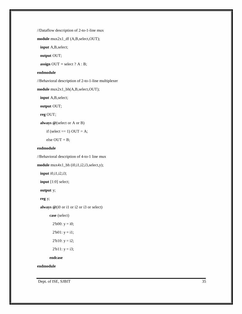
//Dataflow description of 2-to-1-line mux
module mux2x1_df (A,B,select,OUT);
input A,B,select;
output OUT;
assign OUT = select ? A : B;
endmodule
//Behavioral description of 2-to-1-line multiplexer
module mux2x1_bh(A,B,select,OUT);
input A,B,select;
output OUT;
reg OUT;
always @(select or A or B)
if (select == 1) OUT = A;
else OUT = B;
endmodule
//Behavioral description of 4-to-1 line mux
module mux4x1_bh (i0,i1,i2,i3,select,y);
input i0,i1,i2,i3;
input [1:0] select;
output y;
reg y;
always @(i0 or i1 or i2 or i3 or select)
case (select)
2'b00: y = i0;
2'b01: y = i1;
2'b10: y = i2;
2'b11: y = i3;
endcase
endmodule

Dept. of ISE, SJBIT 36
Logic Design 10CS33

Dept. of ISE, SJBIT 37
Logic Design. 10CS33
Adders
Adders are the basic building blocks of all arithmetic circuits; adders add two binary numbers and
give out sum and carry as output. Basically we have two types of adders.
Half Adder.
Full Adder
Half Adder
Adding two single-bit binary values X, Y produces a sum S bit and a carry out C-out bit. This
operation is called half addition and the circuit to realize it is called a half adder.
X Y SUM CARRY
0 0 0 0
0 1 1 0
1 0 1 0
1 1 0 1
S (X,Y) = (1,2)
S = X'Y + XY'
S = X Y
CARRY(X,Y) = (3)
CARRY = XY

Dept. of ISE, SJBIT 38
Logic Design. 10CS33
Full Adder
Full adder takes a three-bits input. Adding two single-bit binary values X, Y with a carry input bit C-
in produces a sum bit S and a carry out C-out bit.
X Y Z SUM CARRY
0 0 0 0 0
0 0 1 1 0
0 1 0 1 0
0 1 1 0 1
1 0 0 1 0
1 0 1 0 1
1 1 0 0 1
1 1 1 1 1
SUM (X,Y,Z) = (1,2,4,7)
CARRY (X,Y,Z) = (3,5,6,7)
Kmap-SUM
SUM = X'Y'Z + XY'Z' + X'YZ'
SUM = X Y Z

Dept. of ISE, SJBIT 39
Logic Design. 10CS33
Kmap-CARRY
CARRY = XY + XZ + YZ
Circuit-SUM
Circuit-CARRY
3.4 Multipliers
Multiplication is achieved by adding a list of shifted multiplicands according to the digits of the
multiplier. An n-bit X n-bit multiplier can be realized in combinational circuitry by using an array of
n-1 n-bit adders where each adder is shifted by one position. For each adder one input is the shifted

Dept. of ISE, SJBIT 40
multiplicand multiplied by 0 or 1 (using AND gates) depending on the multiplier bit, the other input is
n partial product bits.
Dividers
The binary divisions are performed in a very similar manner to the decimal divisions, as shown in the
below figure examples. Thus, the second number is repeatedly subtracted from the figures of the first
number after being multiplied either with '1' or with '0'. The multiplication bit ('1' or '0') is selected for
each subtraction step in such a manner that the subtraction result is not negative. The division result is
composed from all the successive multiplication bits while the remainder is the result of the last
subtraction step.
This algorithm can be implemented by a series of subtracters composed of modified elementary cells.
Each subtracter calculates the difference between two input numbers, but if the result is negative the
operation is canceled and replaced with a subtraction by zero. Thus, each divider cell has the normal
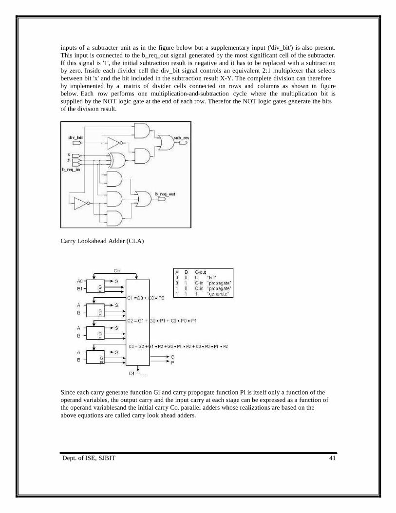
Dept. of ISE, SJBIT 41
inputs of a subtracter unit as in the figure below but a supplementary input ('div_bit') is also present.
This input is connected to the b_req_out signal generated by the most significant cell of the subtracter.
If this signal is '1', the initial subtraction result is negative and it has to be replaced with a subtraction
by zero. Inside each divider cell the div_bit signal controls an equivalent 2:1 multiplexer that selects
between bit 'x' and the bit included in the subtraction result X-Y. The complete division can therefore
by implemented by a matrix of divider cells connected on rows and columns as shown in figure
below. Each row performs one multiplication-and-subtraction cycle where the multiplication bit is
supplied by the NOT logic gate at the end of each row. Therefor the NOT logic gates generate the bits
of the division result.
Carry Lookahead Adder (CLA)
Since each carry generate function Gi and carry propogate function Pi is itself only a function of the
operand variables, the output carry and the input carry at each stage can be expressed as a function of
the operand variablesand the initial carry Co. parallel adders whose realizations are based on the
above equations are called carry look ahead adders.

Dept. of ISE, SJBIT 42
Combinational
Logic Circuit
Unit-4 : Clocks , Flip Flops
Introduction :
Logic circuit is divided into two types.
1. Combinational Logic Circuit
2. Sequential Logic Circuit
4.1 Definition :
1. Combinational Logic Circuit :
The circuit in which outputs depends on only present value of inputs. So it is possible to
describe each output as function of inputs by using Boolean expression. No memory element
involved. No clock input. Circuit is implemented by using logic gates. The propagation delay
depends on, delay of logic gates. Examples of combinational logic circuits are : full adder,
subtractor, decoder, codeconverter, multiplexers etc.
inputs outputs
2. Sequential Circuits :
Sequential Circuit is the logic circuit in which output depends on present value of inputs at
that instant and past history of circuit i.e. previous output. The past output is stored by using
memory device. The internal data stored in circuit is called as state. The clock is required for
synchronization. The delay depends on propagation delay of circuit and clock frequency. The
examples are flip-flops, registers, counters etc.
inputs outputs
Combinational
Logic Circuit
Memory Device
Dept. of ISE, SJBIT 43
Basic Bistable element.
o Flip-Flop is Bistable element.
o It consist of two cross coupled NOT Gates.
o It has two stable states.
o Q and Q are two outputs complement of each other.
o The data stored 1 or 0 in basic bistable element is state of flip-flop.
o 1 – State is set condition for flip-flop.
o 0 – State is reset / clear for flip-flop.
o
Latches :
It stores 1 or 0 state as long power is ON.
S-R Latch : Set-reset Flip-Flop
Latch is a storage device by using Flip-Flop.
Latch can be controlled by direct inputs.
Latch outputs can be controlled by clock or enable input.
Q and Q are present state for output.
Q+
and Q+
are next states for output.
The function table / Truth table gives relation between inputs and outputs.
The S=R=1 condition is not allowed in SR FF as output is unpredictable.
Application of SR Latch :
Bouncing problem with Push button switch.
Debouncing action.
A switch debouncer

Dept. of ISE, SJBIT 44
SR Flip-Flop as switch debouncer.
4.2 Gated SR Latch :
Enable input C is clock input.
C=1, Output changes as per input condition.
C=0, No change of state.
S=1, R=0 is set condition for Flip-flop.
S=0, R=1 is reset condition for Flip-flop.
S=R=1 is ambiguous state, not allowed.
4.3 JK Flip-Flop by using SR Flip-Flop
In SR FF, S=R=1 condition is not allowed.
JK FF is modified version of SR FF.

Dept. of ISE, SJBIT 45
Due to feedback from output to input AND Gate J=K=1 is toggle condition for JK FF.
The output is complement of the previous output.
This condition is used in counters.
T-FF is modified version of JK FF in which T=J=K=1.
Gated D Latch :
D Flip-Flop is Data Flip-Flop.
D Flip-Flop stores 1 or 0.
R input is complement of S.
Only one D input is present.
D Flip-Flop is a storage device used in register.

Logic Design. 10CS33
4.4 Master slave SR Flip-Flop
Two SR Flip-Flop, 1st
is Master and 2nd
is slave.
Master Flip-Flop is positive edge triggered.
Slave Flip-Flop is negative edge triggered.
Slave follows master output.
The output is delayed.
Dept. of ISE, SJBIT 46
Dept. of ISE, SJBIT 47
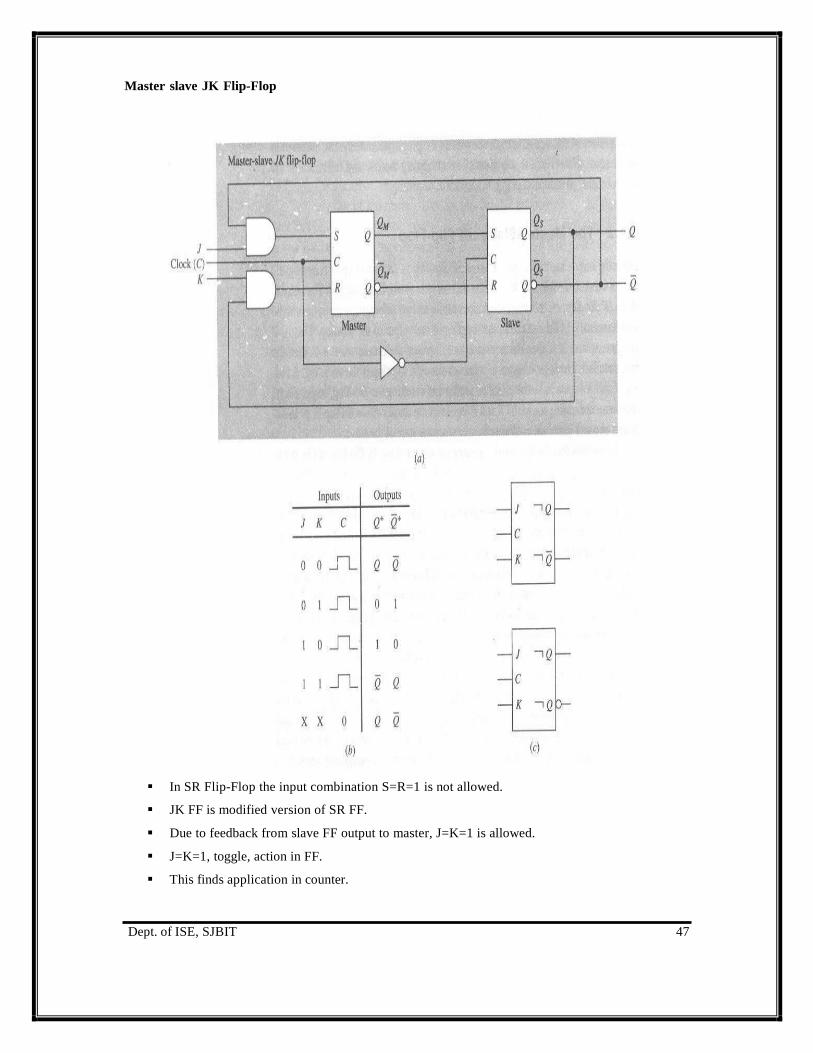
Master slave JK Flip-Flop
In SR Flip-Flop the input combination S=R=1 is not allowed.
JK FF is modified version of SR FF.
Due to feedback from slave FF output to master, J=K=1 is allowed.
J=K=1, toggle, action in FF.
This finds application in counter.

Dept. of ISE, SJBIT 48
4.5 Positive Edge Triggered D Flip-Flop
When C=0, the output of AND Gate 2 & 3 is equal to 1.
If C=1, D=1, the output of AND Gate 2 is 0 and 3 is 1.
S = 0,R = 1, Q = 1 and Q = 0
S = R = 1, No Change of State

Dept. of ISE, SJBIT 49
4.6 HDL implementation of Flip-flops
module D_latch(Q,D,control);
output Q;
input D,control;
reg Q;
always @(control or D)
if(control) Q = D; //Same as: if(control=1)
endmodule
//D flip-flop module D_FF (Q,D,CLK);
output Q;
input D,CLK;
reg Q;
always @(posedge CLK)
Q = D;
endmodule
//JK flip-flop from D flip-flop and gates module JKFF (Q,J,K,CLK,RST);
output Q;
input J,K,CLK,RST;
wire JK;
assign JK = (J & ~Q) | (~K & Q);
//Instantiate D flipflop
DFF JK1 (Q,JK,CLK,RST);
endmodule
// Functional description of JK // flip-flop
module JK_FF (J,K,CLK,Q,Qnot);
output Q,Qnot;
input
reg Q;
J,K,CLK;
assign Qnot = ~ Q ;
always @(posedge CLK)
case({J,K})
2'b00: Q = Q;
2'b01: Q = 1'b0;
2'b10: Q = 1'b1;
2'b11: Q = ~ Q;
endcase
endmodule

Dept. of ISE, SJBIT 50
Unit-5 : Registers
An n-bit register is a collection of n D flip-flops with a common clock used to store n related
bits.
5.1 Types of Register:
Register is a group of Flip-Flops.
It stores binary information 0 or 1.
It is capable of moving data left or right with clock pulse.
Registers are classified as
• Serial-in Serial-Out
• Serial-in parallel Out
• Parallel-in Serial-Out
• Parallel-in parallel Out
Parallel-in Unidirectional Shift Register
![Cse III Logic Design [10cs33] Notes](https://static.fdocuments.us/doc/165x107/55cf9c1f550346d033a8b068/cse-iii-logic-design-10cs33-notes.jpg)