
SX1308 - Astute Electronics
35
SX1308 WIRELESS & SENSING PRODUCTS Datasheet V1.2 June 2017 www.semtech.com 1 DDR - LoRa DDR - LoRa DDR - LoRa 8x LoRa (G)FSK (G)FSK/LoRa Packet handler MCU SX1308 SPI Packet handler Control Tx/Rx (Tx/Rx) (GPS) I/Q I/Q I/Q I/Q timestamp General Description The SX1308 digital baseband chip is a massive digital signal processing engine specifically designed to offer breakthrough gateway capabilities in the ISM bands worldwide. It integrates the LoRa concentrator IP. The LoRa concentrator is a multi-channel high performance transmitter/receiver designed to simultaneously receive several LoRa packets using random spreading factors on random channels. Its goal is to enable robust connection between a central wireless data concentrator and a massive amount of wireless end-points spread over a very wide range of distances. The SX1308 is targeted at smart metering fixed networks and Internet of Things applications. Ordering Information Part Number Conditioning SX1308IMLTRT Tape & Reel 3,000 parts per reel Pb-free, Halogen free, RoHS/WEEE compliant product Key Product Features • Up to -139 dBm sensitivity with SX1257 or SX1255 Tx/Rx front-end • 70 dB CW interferer rejection at 1 MHz offset • Able to operate with negative SNR • CCR up to 9 dB • Emulates 49x LoRa demodulators and 1x (G)FSK demodulator • Dual digital Tx & Rx radio front-end interfaces • 10 programmable parallel demodulation paths • Dynamic data-rate adaptation (ADR) • True antenna diversity or simultaneous dual-band operation Applications • Smart Metering • Security Sensors Network • Agricultural Monitoring • Internet of Things (IoT)
Transcript of SX1308 - Astute Electronics

SX1308
WIRELESS & SENSING PRODUCTS Datasheet
V1.2 June 2017 www.semtech.com 1
DDR - LoRaDDR - LoRaDDR - LoRa8x
LoRa
(G)FSK
(G)FSK/LoRa
Pack
et h
andl
er
MCU
SX1308
SPIPacket handler
Cont
rolTx/Rx
(Tx/Rx)
(GPS)
I/Q
I/Q
I/Q
I/Q
timestamp
General Description
The SX1308 digital baseband chip is a massive digital signal processing engine specifically designed to offer breakthrough gateway capabilities in the ISM bands worldwide. It integrates the LoRa concentrator IP.
The LoRa concentrator is a multi-channel high performance transmitter/receiver designed to simultaneously receive several LoRa packets using random spreading factors on random channels. Its goal is to enable robust connection between a central wireless data concentrator and a massive amount of wireless end-points spread over a very wide range of distances.
The SX1308 is targeted at smart metering fixed networks and Internet of Things applications.
Ordering Information
Part Number Conditioning SX1308IMLTRT Tape & Reel
3,000 parts per reel
Pb-free, Halogen free, RoHS/WEEE compliant product
Key Product Features
• Up to -139 dBm sensitivity with SX1257 or SX1255 Tx/Rx front-end
• 70 dB CW interferer rejection at 1 MHz offset
• Able to operate with negative SNR • CCR up to 9 dB
• Emulates 49x LoRa demodulators and 1x (G)FSK demodulator
• Dual digital Tx & Rx radio front-end interfaces
• 10 programmable parallel demodulation paths
• Dynamic data-rate adaptation (ADR) • True antenna diversity or simultaneous
dual-band operation
Applications
• Smart Metering • Security Sensors Network • Agricultural Monitoring • Internet of Things (IoT)
SX1308
WIRELESS & SENSING PRODUCTS Datasheet
V1.2 June 2017 www.semtech.com 2
Contents
1 PIN CONFIGURATION .................................................................................................................. 4 1.1 Pins Placement and Circuit Marking ........................................................................................... 4 1.2 Pins Description .......................................................................................................................... 5
2 ELECTRICAL CHARACTERISTICS ................................................................................................... 7 2.1 Absolute Maximum Ratings ........................................................................................................ 7 2.2 Constraints on External ............................................................................................................... 7 2.3 Operating Conditions .................................................................................................................. 7 2.4 Electrical Specifications ............................................................................................................... 8 2.5 Timing Specifications .................................................................................................................. 8
3 CIRCUIT OPERATION ................................................................................................................... 9 3.1 General Presentation .................................................................................................................. 9 3.2 Power-On .................................................................................................................................... 9 3.2.1 Power-Up Sequence ................................................................................................................ 9 3.2.2 Setting the Circuit is Low-Power Mode .................................................................................. 9 3.3 Clocking ..................................................................................................................................... 10 3.4 SPI Interface .............................................................................................................................. 11 3.5 Rx I/Q Interface ......................................................................................................................... 12 3.5.1 I/Q Generated on Clock Rising Edge ..................................................................................... 12 3.5.2 I/Q Generated on Clock Falling Edge .................................................................................... 12 3.6 RX Mode Block Diagram, Reception Paths Characteristics ....................................................... 13 3.6.1 Block Diagram ....................................................................................................................... 13 3.6.2 Reception Paths Characteristics ............................................................................................ 14 3.7 Packet Engine and Data Buffers ................................................................................................ 15 3.7.1 Receiver Packet Engine ......................................................................................................... 15 3.7.2 Transmitter Packet Engine .................................................................................................... 17 3.8 Receiver IF Frequencies Configuration ..................................................................................... 19 3.8.1 Configuration Using 2 x SX1257 Radios ................................................................................ 19 3.8.2 Two SX1255: 433 MHz Band ................................................................................................. 21 3.8.3 One SX1257 and one SX1255 ................................................................................................ 21 3.9 Connection to RF Front End ...................................................................................................... 22 3.9.1 Connection to Semtech SX1255 or SX1257 Components ..................................................... 22 3.9.2 SX1308 RX Operation Using a Third Party RF Front End ....................................................... 22 3.9.3 Radio Calibration ................................................................................................................... 24 3.9.4 SX1308 Connection to RF Front End for TX Operation ......................................................... 24 3.10 Reference Application ............................................................................................................... 26 3.11 Hardware Abstraction Layer (HAL) ........................................................................................... 27 3.11.1 Introduction .......................................................................................................................... 27 3.11.2 Abstraction Presented to the Gateway Host ........................................................................ 27
4 EXTERNAL COMPONENTS ......................................................................................................... 29
5 PCB LAYOUT CONSIDERATIONS ................................................................................................ 30
6 PACKAGING INFORMATION ...................................................................................................... 32 6.1 Package Outline Drawing .......................................................................................................... 32 6.2 Thermal Impedance of Package ................................................................................................ 32 6.3 Land Pattern Drawing ............................................................................................................... 33
7 REVISION INFORMATION .......................................................................................................... 34

SX1308
WIRELESS & SENSING PRODUCTS Datasheet
V1.2 June 2017 www.semtech.com 3
Figures
Figure 1: Top View of SX1308 Package with 64 Pins & Exposed Ground Paddle (Package Bottom) ...... 4 Figure 2: Power-up Sequence ................................................................................................................. 9 Figure 3: SPI Timing Diagram (single access) ........................................................................................ 11 Figure 4: I/Q on Clock Rising Edge ........................................................................................................ 12 Figure 5: I/Q on Clock Falling Edge ....................................................................................................... 12 Figure 6: SX1308 Digital Baseband Chip Block Diagram ....................................................................... 13 Figure 7: Access FIFO and Data Buffer .................................................................................................. 16 Figure 8: SX1255/57 Digital I/Q Power Spectral Density ...................................................................... 19 Figure 9: Radio Spectrum ...................................................................................................................... 20 Figure 10: Radio Spectrum .................................................................................................................... 20 Figure 11: Radio Spectrum .................................................................................................................... 21 Figure 12: Dual Band Operation ............................................................................................................ 22 Figure 13: SX1308 with Third Party Front End ...................................................................................... 23 Figure 14: Digital Interface for Third Party Radio ................................................................................. 23 Figure 15: Transmission Schematics ..................................................................................................... 25 Figure 16: Reference Application .......................................................................................................... 26 Figure 17: PCB Layout Example ............................................................................................................. 31 Figure 18: Package Dimensions ............................................................................................................ 32 Figure 19: Land Pattern Drawing .......................................................................................................... 33
Tables
Table 1: Pins Name and Description ....................................................................................................... 6 Table 2: Absolute Maximum Ratings ...................................................................................................... 7 Table 3: Externals .................................................................................................................................... 7 Table 4: Operating Conditions for Electrical Specifications .................................................................... 7 Table 5: Electrical Specifications ............................................................................................................. 8 Table 6: Timing Specifications ................................................................................................................. 8 Table 7: Packet Data Fields ................................................................................................................... 17 Table 8: Packet Structure for Transmission .......................................................................................... 18 Table 9: IF Frequencies Set ................................................................................................................... 20 Table 10: IF Frequency Used ................................................................................................................. 21 Table 11: Recommended External Components .................................................................................. 29

SX1308
WIRELESS & SENSING PRODUCTS Datasheet
V1.2 June 2017 www.semtech.com 4
1 Pin Configuration
1.1 Pins Placement and Circuit Marking
1
16
17 32
64 49
48
33
SX1308yyww
xxxxxxxx
Legend: yyww is the date code and xxxxxxxx is the Semtech lot number.
Figure 1: Top View of SX1308 Package with 64 Pins & Exposed Ground Paddle (Package Bottom)
The ground paddle must be connected to ground potential through a large conductive plane that also serves for temperature dissipation.

SX1308
WIRELESS & SENSING PRODUCTS Datasheet
V1.2 June 2017 www.semtech.com 5
1.2 Pins Description
The table below gives the description of the pins of the circuit.
Pin Pin Name Type Description 0 VSS Power (GND) Ground paddle – must be connected to ground for thermal dissipation 1 RESET Input Global asynchronous reset 2 HOST_SCK Input HOST SPI clock (max 10 MHz clock) 3 HOST_MISO Output HOST SPI Interface 4 HOST_MOSI Input HOST SPI Interface 5 HOST_CSN Input HOST SPI Interface 6 SCANMODE Input Scanmode signal (tied to 0 in normal mode) 7 VSS Power (GND) Ground 8 VCC18 Power (VDD) Logic core supply 9 GPS_IN Input GPS 1 pps input
10 VSS Power (GND) Ground 11 VSS Power (GND) Ground 12 VCC18 Power (VDD) Logic core supply 13 RADIO_A_EN Output Radio A global enable 14 LNA_A_CTRL Output LNA A enable 15 PA_A_CTRL Output PA A enable 16 NC Not connected – tie to VSS 17 PA_GAIN[1] Output PA gain control of both radio A/B 18 PA_GAIN[0] Output PA gain control of both radio A/B 19 RADIO_B_CS Output Radio B SPI interface 20 RADIO_B_MOSI Output Radio B SPI interface 21 RADIO_B_MISO Input Radio B SPI interface 22 RADIO_B_SCK Output Radio B SPI interface 23 VCC18 Power (VCC) Logic core supply 24 VSS Power (GND) Ground 25 RADIO_RST Output Radio A/B global reset 26 PA_B_CTRL Output PA B enable 27 LNA_B_CTRL Output LNA B enable 28 RADIO_B_EN Output Radio B global enable 29 VCC33 Power (VCC) Logic IO supply 30 VSS Power (GND) Ground 31 VSS Power (GND) Ground 32 NC Not connected – tie to VSS 33 NC Not connected – tie to VSS 34 SP_VALID Input Radio C sample valid 35 B_IQ_RX Input Radio B 1 bit I/Q Rx samples 36 B_QI_RX Input Radio B 1 bit Q/I Rx samples 37 B_IQ_TX Output Radio B 1 bit I/Q Tx samples 38 B_QI_TX Output Radio B 1 bit Q/I Tx samples 39 SP_CLK_OUT Output Radio C clock out (32 MHz)

SX1308
WIRELESS & SENSING PRODUCTS Datasheet
V1.2 June 2017 www.semtech.com 6
Pin Pin Name Type Description 40 GND Power (GND) Ground 41 GND Power (GND) Ground 42 VCC18 Power (VCC) Logic core supply 43 CLK32M Input 32 MHz clock from radios crystal 44 A_IQ_RX Input Radio A 1 bit I/Q Rx samples 45 A_QI_RX Input Radio A 1 bit Q/I Rx samples 46 A_IQ_TX Output Radio A 1 bit I/Q Tx samples 47 A_QI_TX Output Radio A 1 bit Q/I Tx samples 48 NC No connected – tie to VSS 49 NC No connected – tie to VSS 50 VSS Power (GND) Ground 51 VSS Power (GND) Ground 52 VCC33 Power (VCC) Logic IO supply 53 CLKHS Input High speed digital clock 54 GPIO[4] In/Out General purpose GPIO[4] 55 GPIO[3] In/Out General purpose GPIO[3] 56 GPIO[2] In/Out General purpose GPIO[2] 57 GPIO[1] In/Out General purpose GPIO[1] 58 GPIO[0] In/Out General purpose GPIO[0] 59 VSS Power (GND) Ground 60 VCC18 Power (VCC) Logic core supply 61 RADIO_A_SCK Output Radio A SPI interface 62 RADIO_A_MISO Input Radio A SPI interface 63 RADIO_A_MOSI Output Radio A SPI interface 64 RADIO_A_CS Output Radio A SPI interface
Table 1: Pins Name and Description

SX1308
WIRELESS & SENSING PRODUCTS Datasheet
V1.2 June 2017 www.semtech.com 7
2 Electrical Characteristics
2.1 Absolute Maximum Ratings
Stresses above the values listed below may cause permanent device failure. Exposure to absolute maximum ratings for extended periods may affect device reliability. Operation outside the parameters specified in the Operating Conditions section is not implied.
Parameter Symbol Conditions Value IO power supply to VSS VDDIO,ABSMAX -0.5 V to 4.0 V Core power supply to VSS VDDCORE,ABSMAX -0.5 V to 2.0 V Storage temperature TJ,STORE -50 °C to 150 °C Junction temperature TJ,ABSMAX -40 °C to 125 °C Pin voltage on IO and Clock pins VDPIN,ABSMAX -0.3 V to VDDIO + 0.3 V Peak reflow temperature TPKG 260 °C Latchup ILUP JESD78D, class I +/-100 mA Humidity HR 0 – 95 % ESD HBM Human Body Model
JESD22-A114 CLASS 2 2 kV
CDM Charged Device Model JESD22-C101 CLASS III
300 V
Table 2: Absolute Maximum Ratings
2.2 Constraints on External
Circuit is expected to be used with the following external conditions.
Parameter Symbol Conditions Min Typ Max Unit Radio ADC samples clock input
frequency XTAL32F Clock for data communication
with Tx† 32 MHz
ADC sample clock frequency tolerance
XTAL32T -10 +10 ppm
High speed processing clock HSC_F Clock for data processing 130 133 150 MHz Load on IO pins CLOP 0 25 pF Notes: † The data communication IOs are A_I_RX, A_Q_RX, B_X_RX, B_Q_RX and clock signal is CLK32M Table 3: Externals
2.3 Operating Conditions
The circuit will operate full specs within the following operating conditions.
Parameter† Symbol Conditions Min Typ Max Unit Digital IO supply
VDDIO Operating Conditions for Electrical Specification
3.0 3.6 V
Digital core supply
VDDCORE Operating Conditions for Electrical Specification
1.75 1.85 V
Ambient operating temperature TA With chip paddle soldered to PCB ground plan with minimum 100 cm2 air
exposed area and heat sink
0 70 °C
Table 4: Operating Conditions for Electrical Specifications

SX1308
WIRELESS & SENSING PRODUCTS Datasheet
V1.2 June 2017 www.semtech.com 8
2.4 Electrical Specifications
The table below gives the specifications of the circuit within the Operating Conditions as indicated in 2.3 unless otherwise specified.
Parameter Symbol Conditions Min Typ Max Unit Current Consumption Current in idle mode
IVDDCORE,IDLE 1.8V supply current in Idle mode1
120 5000 uA
IVDDIO,IDLE 3.3V supply current in idle mode
1 2 uA
Current in medium active IVDDCORE,MED 1.8V supply current with 4 active paths
330 600 mA
IVDDIO,MED 3.3V supply current with 4 active paths – no load
5 10 mA
Current in full active IVDDCORE,FULL 1.8V supply current with 8 active paths
550 800 mA
IVDDIO,FULL 3.3V supply current with 8 active paths – no load
5 10 mA
IO Pins levels Logic low input threshold VIL “0” logic input 0.4 V Logic high input threshold VIH “1” logic input VDDIO
– 0.4 V
Logic low output level VOL “0” logic output, 2 mA sink VSS VSS + 0.4
V
Logic high output level VOH “1” logic output, 2 mA source
VDDIO – 0.4
VDDIO V
Table 5: Electrical Specifications
2.5 Timing Specifications
The table below gives the specifications of the circuit within the Operating Conditions as indicated in 2.3 unless otherwise specified. See chapters 3.4 and 3.5 for timing diagrams and symbol definitions.
Parameter Symbol Conditions Min Typ Max Unit SPI SCK frequency FSCK - - 10 MHz SCK high time tch 50 - - ns SCK low time tcl 50 - - ns SCK rise time trise - 5 - ns SCK fall time tfall - 5 - ns MOSI setup time tsetup From MOSI change to SCK
rising edge. 10 - - ns
MOSI hold time thold From SCK rising edge to MOSI change.
20 - - ns
CSN setup time tnsetup From CSN falling edge to SCK rising edge
10 - - ns
CSN hold time tnhold From SCK falling edge to CSN rising edge, normal mode
40 - - ns
CSN high time between SPI accesses
tnhigh 40 - - ns
Clock to Rx I-Q data Rx IQ hold and setup time tIQ 2 - - ns Table 6: Timing Specifications
1 Idle current is reached following procedure indicated in application part of datasheet (chapter 3.2.2)
SX1308
WIRELESS & SENSING PRODUCTS Datasheet
V1.2 June 2017 www.semtech.com 9
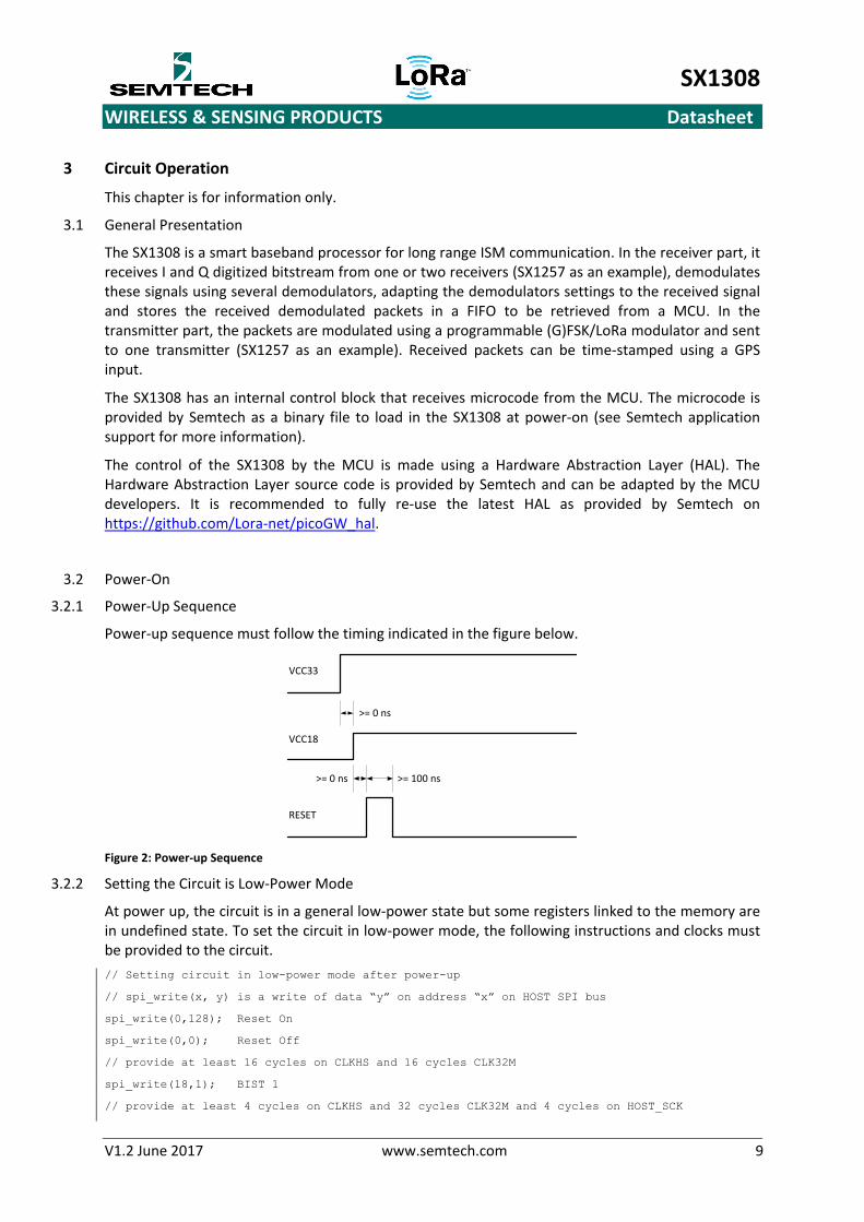
3 Circuit Operation
This chapter is for information only.
3.1 General Presentation
The SX1308 is a smart baseband processor for long range ISM communication. In the receiver part, it receives I and Q digitized bitstream from one or two receivers (SX1257 as an example), demodulates these signals using several demodulators, adapting the demodulators settings to the received signal and stores the received demodulated packets in a FIFO to be retrieved from a MCU. In the transmitter part, the packets are modulated using a programmable (G)FSK/LoRa modulator and sent to one transmitter (SX1257 as an example). Received packets can be time-stamped using a GPS input.
The SX1308 has an internal control block that receives microcode from the MCU. The microcode is provided by Semtech as a binary file to load in the SX1308 at power-on (see Semtech application support for more information).
The control of the SX1308 by the MCU is made using a Hardware Abstraction Layer (HAL). The Hardware Abstraction Layer source code is provided by Semtech and can be adapted by the MCU developers. It is recommended to fully re-use the latest HAL as provided by Semtech on https://github.com/Lora-net/picoGW_hal.
3.2 Power-On
3.2.1 Power-Up Sequence
Power-up sequence must follow the timing indicated in the figure below.
>= 0 ns
>= 0 ns >= 100 ns
VCC33
VCC18
RESET
Figure 2: Power-up Sequence
3.2.2 Setting the Circuit is Low-Power Mode
At power up, the circuit is in a general low-power state but some registers linked to the memory are in undefined state. To set the circuit in low-power mode, the following instructions and clocks must be provided to the circuit. // Setting circuit in low-power mode after power-up
// spi_write(x, y) is a write of data “y” on address “x” on HOST SPI bus
spi_write(0,128); Reset On
spi_write(0,0); Reset Off
// provide at least 16 cycles on CLKHS and 16 cycles CLK32M spi_write(18,1); BIST 1
// provide at least 4 cycles on CLKHS and 32 cycles CLK32M and 4 cycles on HOST_SCK

SX1308
WIRELESS & SENSING PRODUCTS Datasheet
V1.2 June 2017 www.semtech.com 10
spi_write(18,2); BIST 2
// provide at least 4 cycles CLK32M and 4 cycles on HOST_SCK spi_write(0,128); Reset On
spi_write(0,0); Reset Off
Idle mode sequence after power-up
3.3 Clocking
The SX1308 gateway requires two clocks.
• A 32MHz clock synchronous with the ADC samples. This clock is used to internally sample the ADC samples and clock all the decimation filters. When the SX1308 is used with a Semtech S1257 or SX1255 RF front-end, this clock is provided by the radio. This clock uses CMOS levels (0 – 3.3 V). If a third party radio front-end is used, this must be the clock that also clocks the ADCs and serves as a reference for the radio PLLs.
• A high speed clock whose frequency can be anywhere in the range 130 - 150 MHz. This clock uses CMOS level and must be provided from an external Oscillator. There is no constraint on this clock jitter. This clock is used for most of the demodulation blocks and data processing. This clock is never used by any of the analog/radio blocks.

SX1308
WIRELESS & SENSING PRODUCTS Datasheet
V1.2 June 2017 www.semtech.com 11
3.4 SPI Interface
The SPI interface gives access to the configuration register via a synchronous full-duplex protocol. Only the slave side is implemented.
Three access modes to the registers are provided:
• SINGLE access: an address byte followed by a data byte is sent for a write access whereas an address byte is sent and a read byte is received for the read access. The CSN pin goes low at the beginning of the frame and goes high after the data byte.
• BURST access: the address byte is followed by several data bytes. The address is automatically incremented internally between each data byte. This mode is available for both read and writes accesses. The CSN pin goes low at the beginning of the frame and stay low between each byte. It goes high only after the last byte transfer.
• FIFO access: if the address byte corresponds to the address of the FIFO, then succeeding data byte will address the FIFO. The address is not automatically incremented but is memorized and does not need to be sent between each data byte. The CSN pin goes low at the beginning of the frame and stay low between each byte. It goes high only after the last byte transfer.
The figure below shows a typical SPI single access to a register.
Figure 3: SPI Timing Diagram (single access)
MOSI is generated by the master on the falling edge of SCK and is sampled by the slave (i.e. this SPI interface) on the rising edge of SCK. MISO is generated by the slave on the falling edge of SCK.
MISO is always low impedance so it cannot be shared with another device.
A transfer is always started by the CSN pin going low.
The first byte is the address byte. It is comprises:
• one wnr bit, which is “1” for write access and “0” for read access. • then seven bits of address, MSB first.
The second byte is a data byte, either sent on MOSI by the master in case of a write access or received by the master on MISO in case of read access. The data byte is transmitted MSB first.
Proceeding bytes may be sent on MOSI (for write access) or received on MISO (for read access) without a rising CSN edge and re-sending the address. In FIFO mode, if the address was the FIFO address then the bytes will be written / read at the FIFO address. In Burst mode, if the address was not the FIFO address, then it is automatically incremented for each new byte received.

SX1308
WIRELESS & SENSING PRODUCTS Datasheet
V1.2 June 2017 www.semtech.com 12
The frame ends when CSN goes high. The next frame must start with an address byte. The SINGLE access mode is therefore a special case of FIFO / BURST mode with only 1 data byte transferred.
During the write access, the byte transferred from the slave to the master on the MISO line is the value of the written register before the write operation.
3.5 Rx I/Q Interface
The Rx I/Q bit stream has to be generated relative to the radio clock (32 MHz).
The SX1308 can manage I/Q generated on both clock rising and falling edges.
3.5.1 I/Q Generated on Clock Rising Edge
To relax the constraint on setup and hold time, it is recommended to use the falling edge of the clock.
To avoid internal setup and hold violation, it is mandatory to avoid I/Q change in a range of +/- 2 ns around clock falling edge
Figure 4: I/Q on Clock Rising Edge
3.5.2 I/Q Generated on Clock Falling Edge
To relax the constraint on setup and hold time, it is recommended to use the rising edge of the clock
To avoid internal setup and hold violation, it is mandatory to avoid I/Q change in a range of +/- 2 ns around clock rising edge
Figure 5: I/Q on Clock Falling Edge

SX1308
WIRELESS & SENSING PRODUCTS Datasheet
V1.2 June 2017 www.semtech.com 13
3.6 RX Mode Block Diagram, Reception Paths Characteristics
3.6.1 Block Diagram
Figure 6: SX1308 Digital Baseband Chip Block Diagram
All chip functionalities can be accessed through a single high speed SPI interface.
The chip integrates two dedicated micro-controllers.
1. A radio AGC MCU. Handling the real time automatic gain control of the entire chain. For this purpose this MCU can control the two radio front-ends through a dedicated SPI master interface. This MCU also handles radio calibration and RX<->TX radio switch
2. A packet arbiter MCU. Assigning the available LoRa modems to the various reception paths. This arbiter can be configured to follow different priority rules based on parameters like data rate of the incoming packet, channel, radio path or signal strength of the incoming packet.
The firmware of those 2 MCUs can be fully programmed at any time through the HOST SPI interface. This firmware is embedded in the Hardware Abstraction Layer provided by Semtech and does not need to be developed by the user.

SX1308
WIRELESS & SENSING PRODUCTS Datasheet
V1.2 June 2017 www.semtech.com 14
3.6.2 Reception Paths Characteristics
The SX1308 digital baseband chip contains 10 programmable reception paths. Those paths have differentiated levels of programmability and allow different use cases. It is important to understand the differences between those demodulation paths to make the best possible use from the system.
IF8 LoRa Channel This channel can be connected to Radio A or B using any arbitrary intermediate frequency within the allowed range. This channel is LoRa only. The demodulation bandwidth can be configured to be 125, 250 or 500 kHz. The data rate can be configured to any of the LoRa available data rates (SF7 to SF12) but, as opposed to IF0 to 7, ONLY the configured data rate will be demodulated. This channel is intended to serve as a high speed backhaul link to other gateways or infrastructure equipment. This demodulation path is compatible with the signal transmitted by the SX1272 & SX1276 chip family.
IF9 (G)FSK Channel Same as previous except that this channel is connected to a GFSK demodulator. The channel bandwidth and bitrate can be adjusted. This demodulator offers a very high level of configurability, going well beyond the scope of this document. The demodulator characteristics are essentially the same than the GFSK demodulator implemented on the SX1232 and SX1272 Semtech chips.
This demodulation path can demodulate any legacy FSK or GFSK formatted signal.
IF0 to IF7 LoRa Channels Those channels can be connected individually to Radio A or B. The channel bandwidth is 125 kHz and cannot be modified or configured. Each channel IF frequency can be individually configured. On each of those channels any data rate can be received without prior configuration. Several packet using different data rates may be demodulated simultaneously even on the same channel. Those channels are intended to be used for a massive asynchronous star network of 10000’s of sensor nodes. Each sensor may use a random channel (amongst IF0 to 7) and a different data rate for any transmission.
Typically sensor located near the gateway will use the highest possible data rate in the fixed 125 kHz channel bandwidth (e.g. 6 kbit/s) while sensors located far away will use a lower data rate down to 300 bit/s (minimum LoRa data rate in a 125 kHz channel).
The SX1308 digital baseband chip scans the 8 channels (IF0 to IF7) for preambles of all data rates at all times. The chip is able to demodulate simultaneously up to 8 packets. Any combination of up to 8 packets is possible (e.g. one SF7 packet on IF0, one SF12 packet on IF7 and one SF9 packet on IF1 simultaneously).
The SX1308 can detect simultaneously preambles corresponding to all data rates on all IF0 to IF7 channels. However it cannot demodulate more than 8 packets simultaneously. This is because the SX1308 architecture separates the preamble detection and acquisition task from the demodulation process. The number of simultaneous demodulation (in this case 8) is an arbitrary system parameter and may be set to any value for a customer specific circuit.
The unique multi data-rate multi-channel demodulation capacity of channels 0 to 7 allow innovative network architecture to be implemented:
• End-point nodes can change frequency with each transmission in a random pattern. This provides vast improvement of the system in term of interferer robustness and radio channel diversity

SX1308
WIRELESS & SENSING PRODUCTS Datasheet
V1.2 June 2017 www.semtech.com 15
• End-point nodes can dynamically perform link rate adaptation based on their link margin without adding to the protocol complexity. There is no need to maintain a table of which end point uses which data rate, because all data rates are demodulated in parallel.
• True antenna diversity can be achieved on the gateway side. Allows better performance for mobile nodes in difficult multi-path environments.
3.7 Packet Engine and Data Buffers
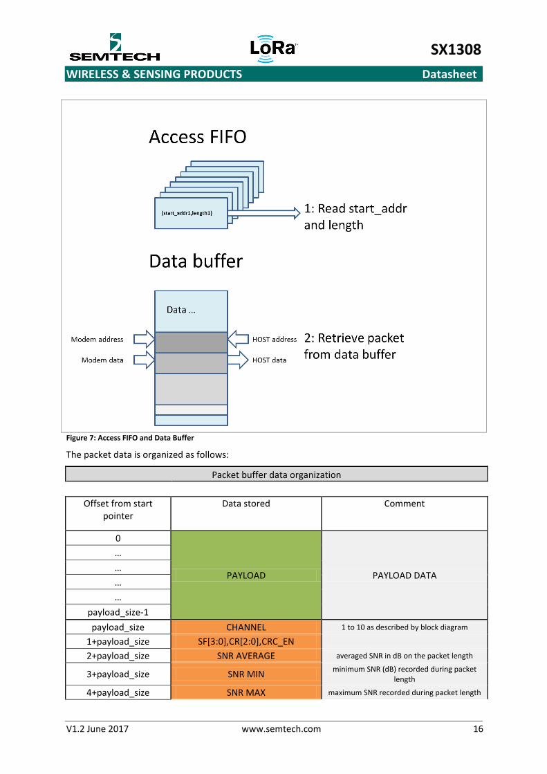
3.7.1 Receiver Packet Engine
Each time any of the demodulators decodes a packet, it is tagged with some additional information and stored in a shared data buffer (the data buffer size is 1024 bytes). For this purpose a specific data buffer management block reserves a segment with the necessary length in the data buffer and at the same time, stores the start address and the length of the packet field in a small FIFO type structure (named the access FIFO). The FIFO can contain up to 16 (start_addr, length) pairs.
A status register contains at any moment the number of packets currently stored in the data buffer (and in the access FIFO).
To retrieve a packet, the host micro-controller first advances 1 step in the access FIFO by writing 1 to the ‘next’ bit. Then reads the (start_addr, length) information. The host micro-controller can now retrieve in one SPI burst operation the entire packet and associated meta-data by reading ‘length’+16 bytes starting at address ‘start_addr’ in the data buffer .. To do so, first position the HOST address pointer to ‘start-addr’, then read ‘length’ + 16 bytes from the ‘packet_data’ register. At the end of each byte the HOST address pointer is automatically incremented.
SX1308
WIRELESS & SENSING PRODUCTS Datasheet
V1.2 June 2017 www.semtech.com 16
Figure 7: Access FIFO and Data Buffer
The packet data is organized as follows:
Packet buffer data organization
Offset from start pointer
Data stored Comment
0
PAYLOAD PAYLOAD DATA
… … … …
payload_size-1 payload_size CHANNEL 1 to 10 as described by block diagram
1+payload_size SF[3:0],CR[2:0],CRC_EN
2+payload_size SNR AVERAGE averaged SNR in dB on the packet length
3+payload_size SNR MIN minimum SNR (dB) recorded during packet length
4+payload_size SNR MAX maximum SNR recorded during packet length

SX1308
WIRELESS & SENSING PRODUCTS Datasheet
V1.2 June 2017 www.semtech.com 17
5+payload_size RSSI channel signal strength in dB averaged during packet
6+payload_size TIMESTAMP[7:0]
32 bits time stamp , 1 us step 7+payload_size TIMESTAMP[15:8] 8+payload_size TIMESTAMP[23:16] 9+payload_size TIMESTAMP[31:24]
10+payload_size CRC_VALUE[7:0] value of the computed CRC16
11+payload_size CRC_VALUE[15:8] 12+payload_size MODEM ID
13+payload_size RX_MAX_BIN_POS[7:0] Correlation peak position
14+payload_size RX_MAX_BIN_POS[15:8] 15+payload_size RX_CORR_SNR Detection correlation SNR
16+payload_size Reserved
17+payload_size Reserved
Table 7: Packet Data Fields
This means that the host micro-processor has to read 16 additional bytes on top of each packet to have access to all the meta-data. If the host is only interested in the payload itself + the channel and the data rate used, then payload + 2bytes is enough.
3.7.2 Transmitter Packet Engine
The SX1308 gateway transmitter can be used to send packets. The following parameters can be dynamically programmed with each packet:
• Radio channel • FSK or LoRa modulation • Bandwidth, data rate, coding rate (in LoRa mode), bit rate and Fdev (in FSK mode) • RF output power • Radio path (A or B) • Time of departure (immediate or differed based on the gateway hardware clock with 1us
accuracy)
All those dynamic parameter fields are sent alongside the payload in the same data buffer.
The data buffer can only hold a single packet at a time (next packet to be sent). The scheduling and ordering task is let to the host micro-processor.
The host micro-processor can program the exact time of departure of each packet relative to the gateway hardware clock. The same clock is used to tag each packet received with a 32bits timestamp. The same 32bits time stamp principle is used in TX mode to indicate when to transmit exactly. This removes the real time constraint from the host micro-processor and allows very precise protocol timing.( For example, if the protocol running on the end point expects and acknowledge exactly one sec after the end of each packet of its uplink). The host micro-processor pulls the uplink packet from the RX packet engine, realizes that it must send an acknowledge, takes the uplink packet time stamp, simply increments it by 1 sec and uses that value to program the time of departure of the acknowledge packet. Exactly one second (+/- 1us) after the uplink packet was received, the gateway will transmit the desired acknowledge packet. This allows very tight reception interval windows on the battery powered end points hence improved battery life.

SX1308
WIRELESS & SENSING PRODUCTS Datasheet
V1.2 June 2017 www.semtech.com 18
The packet structure for transmission is as follow: Byte Subfield Description comment
0 23:16 Channel frequency Fchan/32MHz*2^19 1 15:8
2 7:0 3 31:24
Start time Value of the timer at which the modem has to start (in us)
4 23:16 5 15:8 6 7:0
7
7:6 Reserved 5:5 Radio select Select radio A (0) or B (1) 4:4 Modulation type 0:LoRa, 1:FSK 3:0 Tx power >7: 20dBm, otherwise 14dBm
8 Reserved LoRa:
9 7:7 Payload CRC16 enable Enables CRC16 6:4 Coding rate Coding rate = 4/(4+CR) 3:0 SF 6 to 12
10 7:0 Payload length number of bytes
11 7:3 Reserved 2:2 Implicit header enable 1:0 Modulation bandwidth 2:500, 1:250, 0:125 kHz
12 15:8 Preamble symbol number Number of symbols in the preamble
13 7:0 14 Reserved 15 Reserved
FSK: 9 7:0 FSK frequency deviation Frequency deviation in KHz
10 7:0 Payload length number of bytes
11
0 Packet Mode 0 -> fixed length 1 -> variable length
1 CRC enable 0 -> No CRC 1 -> CRC
3:2 Dcfree Enc
00 -> DC free encoding off 01 -> Manchester encoding 10 -> Whitening Encoding 11 -> reserved
4 Crc IBM 0 -> CCITT CRC 1 -> IBM CRC
12 15:8 FSK Preamble Size The number of preamble bytes sent over the air before the sync pattern. 13 7:0 FSK Preamble Size
14 15:8 FSK bit rate Bit rate = 32e6/(FSK bit rate)
15 7:0 FSK bit rate 16 Payload first byte Up to 128 bytes
Table 8: Packet Structure for Transmission
For words of more than 1 byte, MSBs are sent first.
Bytes 9 to 15 vary depending whether the FSK or the LoRa TX modem is being used.

SX1308
WIRELESS & SENSING PRODUCTS Datasheet
V1.2 June 2017 www.semtech.com 19
The user payload starts at byte 16. This is the first byte that will be received by the end point. Bytes 0 to 15 are not transmitted and are just used to dynamically configure the gateway prior to emission.
3.8 Receiver IF Frequencies Configuration
Each IF path intermediate frequency can be programmed independently from -2 to +2 MHz. The following sections give a few programming examples for various use cases.
3.8.1 Configuration Using 2 x SX1257 Radios
The SX1257 RX PLLs can be configured to any frequency inside the 868/900 MHz ISM band with a 61 Hz step. The SX1257 streams I/Q samples through a 2 wire digital interface. The bits stream corresponds directly to the I/Q sigma delta ADCs outputs sampled at 32 MSps. This delta sigma stream must be low-passed and decimated to recover the available 80dB dynamic of the ADCs. After decimation the usable spectrum bandwidth is ±400 kHz centered on the RX PLL carrier frequency.
The following plot gives the spectral power content of the I/Q bit stream.
Figure 8: SX1255/57 Digital I/Q Power Spectral Density
The quantization noise raises sharply outside the -400 to +400 kHz range. For more details on the SX1257/55 radio specifications please consult the specific product datasheet.
The following plot represents a possible use case where
• Radio A PLL is set to 867.0 MHz • Radio B PLL is set to 868.4 MHz • The system uses 8 separate 125 kHz LoRa channels for star connection to sensors • One high speed 250 kHz LoRa channel for connection to a relay • One high speed 200 kHz GFSK channel for meshing
-8 -6 -4 -2 0 2 4 6 8 10
x 105
-10
0
10
20
30
40
signal power spectral density
dB
Hz (105)

SX1308
WIRELESS & SENSING PRODUCTS Datasheet
V1.2 June 2017 www.semtech.com 20
Figure 9: Radio Spectrum
In the previous example the various IF frequencies would be set as follow:
IF8 A: -125kHz Lora backhaul , fixed data-rate IF9 B: 0kHz GFSK backhaul IF0 A: -312.5kHz LoRa multi-data rate channel IF1 A: 62.5kHz “ IF2 A: 187.5kHz “ IF3 A: 312.5kHz “ IF4 B: -312.5kHz “ IF5 B: -187.5kHz “ IF6 B: 187.5kHz “ IF7 B: 312.5kHz “
Table 9: IF Frequencies Set
If for example, 8 contiguous 125 kHz LoRa channels are desired the following configuration may be used:
• Radio A PLL is set to 867 MHz • Radio B PLL is set to 876.5 MHz
The two radio baseband spectrum overlap a little bit.
Figure 10: Radio Spectrum
The following IF frequencies are used:

SX1308
WIRELESS & SENSING PRODUCTS Datasheet
V1.2 June 2017 www.semtech.com 21
IF8 A: 0 kHz Lora backhaul , fixed data-rate IF9 Not used GFSK backhaul IF0 B: -187.5 kHz LoRa multi-data rate channel IF1 B: -62.5 kHz “ IF2 B: 62.5 kHz “ IF3 B: 187.5 kHz “ IF4 A: -187.5 kHz “ IF5 A: -62.5 kHz “ IF6 A: 62.5 kHz “ IF7 A: 187.5 kHz “
Table 10: IF Frequency Used
Note : As shown in this example the 500 or 250 kHz IF1 LoRa channel may overlap with the multi-data rate IF3 to 10 channels. Transmissions happening in the IF7 to 10 channels will be noise like for the IF1 LoRa demodulator and reciprocally. It is however better from a performance point of view to separate as much as possible different channels mainly when the associated signal powers are very different (like between a backhaul link which usually enjoys line-of-sight attenuation and sensor link with very low signal levels).
3.8.2 Two SX1255: 433 MHz Band
The circuit will behave exactly as described in the previous section except that everything can be transposed in the 433 MHz ISM band using SX1255 front-end radios instead of SX1257.
3.8.3 One SX1257 and one SX1255
In that case dual band simultaneous reception is possible. The following configuration is a typical example of the possible system configuration.
Figure 11: Radio Spectrum
• Radio A is an SX1255 configured on 433.6 MHz • Radio B is a SX1257 configured on 866.4 MHz • 4 multi data-rates 125 kHz LoRa channel in the low –band • 4 multi data-rates 125 kHz LoRa channel in the high –band • One 250 kHz LoRa fixed data-rate channel superposed with a 200 kHz GFSK channel in the
high band
As can be seen the system is extremely flexible and allows any arbitrary set of channel configuration.

SX1308
WIRELESS & SENSING PRODUCTS Datasheet
V1.2 June 2017 www.semtech.com 22
3.9 Connection to RF Front End
3.9.1 Connection to Semtech SX1255 or SX1257 Components
The SX1308 digital baseband chip is designed to be preferably interfaced with either:
1. 2x SX1257 radio front-ends for the 868 MHz band with antenna diversity support 2. 2x SX1255 radio front-ends for the 433 MHz band with antenna diversity support 3. 1x SX1257 & 1x SX1255 , enabling simultaneous dual-band operation
All modems Intermediate Frequencies may be adjusted independently within the allowed radio baseband bandwidth, e.g. ±400 kHz. Optimized firmware is provided to optimally setup the SX1257/55 radios and perform real time automatic gain control.
Figure 12: Dual Band Operation
3.9.2 SX1308 RX Operation Using a Third Party RF Front End
In that case a third party RF front-end may be used. The digitized I/Q stream must be adapted to the specific format required by the SX1308 digital baseband using an FPGA/CPLD or any other suitable programmable component.
In that mode the SX1308 expects a stream of 4 bits samples at a 32 MSps rate. The “Sample valid” input should pulse every 8 clock cycles to delimit packets of 8 samples. From those 8 samples representing 32 bits, the first 24 MSB are kept as I/Q 12bits sample information and fed to the internal sample 4 MSps sample bus.

SX1308
WIRELESS & SENSING PRODUCTS Datasheet
V1.2 June 2017 www.semtech.com 23
All modems Intermediate Frequencies may be adjusted independently within the allowed radio baseband bandwidth up to 2 MHz (third party radio and FPGA/CPLD digital filtering dependent)
The 32MHz clock input is not represented for the sake of clarity.
Figure 13: SX1308 with Third Party Front End
The digital interface to third party radio works as follow:
Figure 14: Digital Interface for Third Party Radio
The RF front-end must provide a 32 MHz clock. ”Sample valid” and data bits must change state on the rising edge of the clock. They are sampled internally in the SX1308 digital IC on the falling edge of the 32 MHz clock.
The “sample valid” signal signals the start of a new I/Q sample. The I/Q ‘bits chunks are time interleaved.
When the SX1308 digital baseband chip is connected to a third party radio front-end, the firmware running on the AGC MCU can be changed to perform dynamic gain adaptation of the external radio chip through an SPI interface. The radio SPI interface must fulfill the following conditions:

SX1308
WIRELESS & SENSING PRODUCTS Datasheet
V1.2 June 2017 www.semtech.com 24
1. 7 bits address width and 1 W/R bit 2. 8 bits data width
The “Chip select” signal polarity is programmable.
3.9.3 Radio Calibration
All calibrations required are performed by uploading the calibration firmware to the integrated radio controller MCU. This specific firmware runs entirely on the SX1308 gateway without intervention of the host micro-processor and performs the following calibrations on both radio channels:
• Carrier leakage cancellation in TX mode • IQ gain (better than 0.1 dB) and phase imbalance (better than 1 deg) in RX mode
All corrections are applied digitally inside the SX1308 gateway at the appropriate place in the TX & RX processing chains.
During the duration of the calibration (500 ms), no RX or TX operation is possible.
3.9.4 SX1308 Connection to RF Front End for TX Operation
In TX mode, the SX1308 digital baseband must be connected either to:
1. At least one SX1255 or SX1257 2. Any combination of both radios
Any LoRa or (G)FSK packet may be transmitted on any of the two radios. Only a single packet may be transmitted at any given time. Transmit operation interrupts all current reception operations.
The digital radio interfaces are separated between RX & TX, therefore the SX1308 may accommodate a third party radio front-end for RX operations and any combination of SX1255/57 for TX operation without problem.

SX1308
WIRELESS & SENSING PRODUCTS Datasheet
V1.2 June 2017 www.semtech.com 25
Figure 15: Transmission Schematics
A third party radio can be supported for TX operations as well. If the third party radio SPI protocol differs from SX1255/57 then the SPI protocol from SX1308 must be adapted to the specific format required by the third party radio using an FPGA/CPLD or any other suitable programmable component. In that mode the digitized I/Q stream from the SX1308 is a sigma delta 1 bit sample at a 32 MSps rate and must also be adapted to the specific format required by the third party radio using an FPGA/CPLD or any other suitable programmable component.

SX1308
WIRELESS & SENSING PRODUCTS Datasheet
V1.2 June 2017 www.semtech.com 26
3.10 Reference Application
Figure 16: Reference Application

SX1308
WIRELESS & SENSING PRODUCTS Datasheet
V1.2 June 2017 www.semtech.com 27
3.11 Hardware Abstraction Layer (HAL)
3.11.1 Introduction
The Semtech SX1308 is an all-digital half-duplex radio modem capable of receiving multiple modulations, multiple radio channels, and multiple data rates simultaneously. This SX1308 is highly configurable.
Because of the variable number (and types) of radio channels, modems and transceivers, and because the different hardware implementations can be quite different (typically, not the same register mapping, naming and various features), presenting a unified Hardware Abstraction Layer (HAL) software to the user can greatly simplify writing an application and porting an application between different hardware.
The SX1308 registers are managed by the HAL software. The HAL software can be found on GitHub at the following address:
https://github.com/Lora-net/picoGW_hal
The hardware supported by the current HAL software is the following:
• SX1308 based board • Two SX1257 radios • FPGA (TX mask baseband filter, Background Spectral Scan state machine and SPI muxing)
and associated SX1272 radio to execute Background Spectral Scan feature • A native SPI link between the gateway host and the SX1308 LoRa concentrator
One example of how to use the HAL software is the packet_forwarder program running on the host of a LoRA gateway. The packet_forwarder program can be found on GitHub at the following address:
https://github.com/Lora-net/picoGW_packet_forwarder
3.11.2 Abstraction Presented to the Gateway Host
The system composed of a SX1308 and one or more radio transceivers is represented to the user as the following entities:
• 1 or more radio chains, • 1 or more RX modems with a settable Intermediate Frequency (IF), • A unified RX packet buffer, • A single TX chain.
The link between the SX1308 and the gateway host is transparent for the user.
Radio Chain A radio chain selects and amplifies a limited portion of the RF spectrum, and digitizes it to be used by the modem chains.
A radio chain is characterized by its bandwidth, maximum and minimum allowed RF frequency in RX, maximum and minimum allowed RF frequency in TX.
Modem Chain A modem chain demodulates a small portion (a RF channel) of the RF spectrum digitized by a radio chain. Each modem chain RF channel can be placed individually inside the bandwidth of a radio using

SX1308
WIRELESS & SENSING PRODUCTS Datasheet
V1.2 June 2017 www.semtech.com 28
the IF (for Intermediate Frequency) setting, that’s why they are designated in the abstraction as “IF+modem” chains.
The modem demodulates packets according to it intrinsic capabilities (e.g. the modulations it can process) and user-selected settings (e.g. what is the channel bandwidth for modems that supports multiple bandwidths) and send the receive packets to the RX buffer.
An IF+modem chain is characterized by its type (e.g. Lora “multi”, FSK “standard”). That type defines what sort of signal can be demodulated and how the settings are interpreted.
RX Buffer Packets that are received by all the modem chains are stored in the RX packet buffer until the gateway host come and fetch them.
TX Chain The TX chain is composed of a single multi-standard, multi-bandwidth, multi-data-rate modem and is used to send the single packet waiting in the TX packet buffer through one of the radio chains.

SX1308
WIRELESS & SENSING PRODUCTS Datasheet
V1.2 June 2017 www.semtech.com 29
4 External Components
A decoupling capacitor (Cdec) is required to minimize the ripple on the power lines.
Component Value Manufacturer Part number Package Cdec 100 nF, 10 V TDK C0603X5R1A104KT 0201 (0603 metric)
100 nF, 6.3 V Taiyo Yuden EMK063AC6104MP-F 0201 (0603 metric) 100 nF, 6.3 V Murata GRM033R60J104ME19D 0201 (0603 metric)
Table 11: Recommended External Components

SX1308
WIRELESS & SENSING PRODUCTS Datasheet
V1.2 June 2017 www.semtech.com 30
5 PCB Layout Considerations
The bottom ground paddle must be soldered to a ground plane. The ground plane must be large enough to support SX1308 power dissipation.
The PCB layout must minimize distances between the IC and the decoupling capacitors.
PCB dimensions: 73mm x 31mm x 1.6mm – 4-layers FR4 with 6x6 via holes.
Caution!
This PCB is size-constrained which has a significant impact on thermal dissipation capabilities. Design integrators should take care of thermal engineering to ensure proper dissipation.
Top Layer - Signals
Mid Layer 1

SX1308
WIRELESS & SENSING PRODUCTS Datasheet
V1.2 June 2017 www.semtech.com 31
Mid Layer 2
Bottom layer – thermal dissipation
Figure 17: PCB Layout Example

SX1308
WIRELESS & SENSING PRODUCTS Datasheet
V1.2 June 2017 www.semtech.com 32
6 Packaging Information
6.1 Package Outline Drawing
MILLIMETERS
0.50 BSC
.002- 0.00.000A1
.350
.350
.276
.276
.012
.007
E1
aaabbb
N
eL
A2
D1D
E
b
.020 BSC.281
.016
.003
.004
64
.354
(.008)
.281
.354
.010-
7.00.285
.020 0.30
.358
.358
.285
-.012
8.90
8.907.00
-0.18
.031MINDIM
AMAX
DIMENSIONSINCHES
-NOM
.039 0.80MIN
- 0.05
9.10
9.10
7.25
7.25
0.50
0.30
7.15
0.40
0.100.0864
9.00
(0.20)
7.159.000.25
-
1.00MAX
-NOM
SEATING PLANE
12
N
COPLANARITY APPLIES TO THE EXPOSED PAD AS WELL AS THE TERMINALS.CONTROLLING DIMENSIONS ARE IN MILLIMETERS (ANGLES IN DEGREES).
NOTES:
2.1.
PIN 1INDICATOR
(LASER MARK)
A1
E
D
A
A2
D/2
A B
Caaa C
ee/2
E1
D1
E/2
LxN
bxNMbbb C A B
Figure 18: Package Dimensions
6.2 Thermal Impedance of Package
Thermal impedance with natural convection is 16.4 °C/W. Thermal impedance with heat sink on package bottom is 0.18 °C/W.
The measurement was made with chip paddle soldered to PCB ground plane with minimum 100 cm² air exposed area and heat sink per JESD51-7. The package is mounted on a 4-layer (2S2P) standard JEDEC board.
SX1308
WIRELESS & SENSING PRODUCTS Datasheet
V1.2 June 2017 www.semtech.com 33
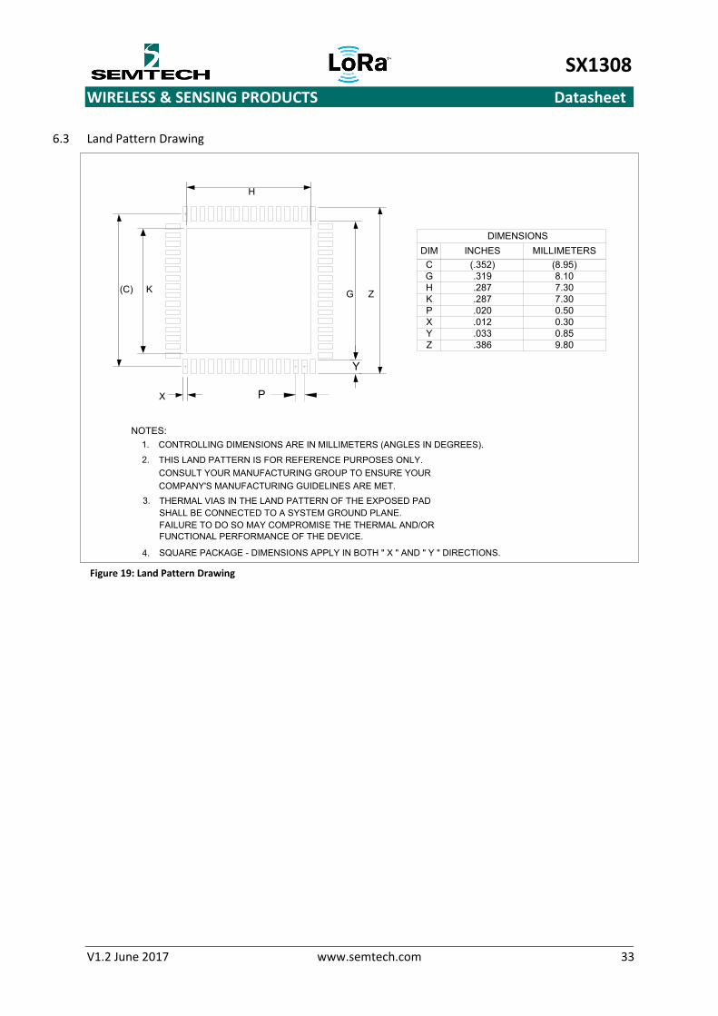
6.3 Land Pattern Drawing
THIS LAND PATTERN IS FOR REFERENCE PURPOSES ONLY.CONSULT YOUR MANUFACTURING GROUP TO ENSURE YOUR
NOTES:
2.
DIM
XY
HKP
CG
MILLIMETERSINCHES(8.95)
.012
.033
.319
.020
.287
.287
(.352)
0.300.85
7.30
0.507.30
8.10
DIMENSIONS
COMPANY'S MANUFACTURING GUIDELINES ARE MET.
9.80.386Z
SQUARE PACKAGE - DIMENSIONS APPLY IN BOTH " X " AND " Y " DIRECTIONS.
FUNCTIONAL PERFORMANCE OF THE DEVICE.FAILURE TO DO SO MAY COMPROMISE THE THERMAL AND/OR SHALL BE CONNECTED TO A SYSTEM GROUND PLANE.THERMAL VIAS IN THE LAND PATTERN OF THE EXPOSED PAD
4.
3.
1. CONTROLLING DIMENSIONS ARE IN MILLIMETERS (ANGLES IN DEGREES).
P
Y
X
(C) G
H
K Z
Figure 19: Land Pattern Drawing

SX1308
WIRELESS & SENSING PRODUCTS Datasheet
V1.2 June 2017 www.semtech.com 34
7 Revision Information
Revision Information
V1.0 First Release
V1.1 Correction of typos
V1.2 First publication on the website
Addition of the environmental data

SX1308
WIRELESS & SENSING PRODUCTS Datasheet
V1.2 June 2017 www.semtech.com 35
© Semtech 2017
All rights reserved. Reproduction in whole or in part is prohibited without the prior written consent of the copyright owner. The information presented in this document does not form part of any quotation or contract, is believed to be accurate and reliable and may be changed without notice. No liability will be accepted by the publisher for any consequence of its use. Publication thereof does not convey nor imply any license under patent or other industrial or intellectual property rights. Semtech assumes no responsibility or liability whatsoever for any failure or unexpected operation resulting from misuse, neglect improper installation, repair or improper handling or unusual physical or electrical stress including, but not limited to, exposure to parameters beyond the specified maximum ratings or operation outside the specified range.
SEMTECH PRODUCTS ARE NOT DESIGNED, INTENDED, AUTHORIZED OR WARRANTED TO BE SUITABLE FOR USE IN LIFE-SUPPORT APPLICATIONS, DEVICES OR SYSTEMS OR OTHER CRITICAL APPLICATIONS. INCLUSION OF SEMTECH PRODUCTS IN SUCH APPLICATIONS IS UNDERSTOOD TO BE UNDERTAKEN SOLELY AT THE CUSTOMER’S OWN RISK. Should a customer purchase or use Semtech products for any such unauthorized application, the customer shall indemnify and hold Semtech and its officers, employees, subsidiaries, affiliates, and distributors harmless against all claims, costs damages and attorney fees which could arise.
Contact Information
Semtech Corporation
Wireless & Sensing Products Division
200 Flynn Road, Camarillo, CA 93012
Phone: (805) 498-2111 Fax: (805) 498-3804
www.semtech.com


