SWRS070B –MARCH 2008–REVISED SEPTEMBER 2014 … · Product Folder Sample & Buy Technical...
25
Product Folder Sample & Buy Technical Documents Tools & Software Support & Community CC2591 SWRS070B – MARCH 2008 – REVISED SEPTEMBER 2014 CC2591 2.4-GHz RF Front End 1 Device Overview 1.1 Features 1 • Seamless Interface to 2.4-GHz Low-Power RF • Digital Control of LNA Gain by HGM Pin Devices from Texas Instruments • 100-nA in Power Down (EN = PAEN = 0) • Output Power up to 22 dBm • Low Transmit Current Consumption • Few External Components (100 mA at 3 V for 20-dBm Out, PAE = 33%) – Integrated Switches • Low-Receive Current Consumption – Integrated Matching Network – 3.4 mA for High-Gain Mode – Integrated Balun – 1.7 mA for Low-Gain Mode – Integrated Inductors • 4.8-dB LNA Noise Figure, Including T/R Switch and External Antenna Match – Integrated PA • RoHS Compliant 4×4-mm QFN-16 Package – Integrated LNA • 2-V to 3.6-V Operation 1.2 Applications • All 2.4-GHz ISM Band Systems • IEEE 802.15.4 and ZigBee ® Systems • Wireless Sensor Networks • Wireless Consumer Systems • Wireless Industrial Systems • Wireless Audio Systems 1.3 Description CC2591 is a cost-effective and high-performance RF front end for low-power and low-voltage 2.4-GHz wireless applications. The device is a range extender for all existing and future 2.4-GHz low-power RF transceivers, transmitters, and System-on-Chip products from TI. CC2591 increases the link budget by providing a power amplifier for increased output power, and an LNA with low noise figure for improved receiver sensitivity. The device provides a small size, high output power RF design with its 4-mm × 4-mm QFN-16 package. The device contains PA, LNA, switches, RF-matching, and balun for simple design of high-performance wireless applications. Device Information (1) PART NUMBER PACKAGE BODY SIZE CC2591RGV RGV (16) 4.00 mm × 4.00 mm (1) For more information, see Section 7, Mechanical Packaging and Orderable Information. 1 An IMPORTANT NOTICE at the end of this data sheet addresses availability, warranty, changes, use in safety-critical applications, intellectual property matters and other important disclaimers. PRODUCTION DATA.
Transcript of SWRS070B –MARCH 2008–REVISED SEPTEMBER 2014 … · Product Folder Sample & Buy Technical...

Product
Folder
Sample &Buy
Technical
Documents
Tools &
Software
Support &Community
CC2591SWRS070B –MARCH 2008–REVISED SEPTEMBER 2014
CC2591 2.4-GHz RF Front End1 Device Overview
1.1 Features1
• Seamless Interface to 2.4-GHz Low-Power RF • Digital Control of LNA Gain by HGM PinDevices from Texas Instruments • 100-nA in Power Down (EN = PAEN = 0)
• Output Power up to 22 dBm • Low Transmit Current Consumption• Few External Components (100 mA at 3 V for 20-dBm Out, PAE = 33%)
– Integrated Switches • Low-Receive Current Consumption– Integrated Matching Network – 3.4 mA for High-Gain Mode– Integrated Balun – 1.7 mA for Low-Gain Mode– Integrated Inductors • 4.8-dB LNA Noise Figure, Including T/R Switch
and External Antenna Match– Integrated PA• RoHS Compliant 4×4-mm QFN-16 Package– Integrated LNA• 2-V to 3.6-V Operation
1.2 Applications• All 2.4-GHz ISM Band Systems • IEEE 802.15.4 and ZigBee® Systems• Wireless Sensor Networks • Wireless Consumer Systems• Wireless Industrial Systems • Wireless Audio Systems
1.3 DescriptionCC2591 is a cost-effective and high-performance RF front end for low-power and low-voltage 2.4-GHzwireless applications. The device is a range extender for all existing and future 2.4-GHz low-power RFtransceivers, transmitters, and System-on-Chip products from TI. CC2591 increases the link budget byproviding a power amplifier for increased output power, and an LNA with low noise figure for improvedreceiver sensitivity. The device provides a small size, high output power RF design with its 4-mm × 4-mmQFN-16 package. The device contains PA, LNA, switches, RF-matching, and balun for simple design ofhigh-performance wireless applications.
Device Information (1)
PART NUMBER PACKAGE BODY SIZECC2591RGV RGV (16) 4.00 mm × 4.00 mm
(1) For more information, see Section 7, Mechanical Packaging and Orderable Information.
1
An IMPORTANT NOTICE at the end of this data sheet addresses availability, warranty, changes, use in safety-critical applications,intellectual property matters and other important disclaimers. PRODUCTION DATA.

PA
Logic
Bias
15 7
2
3
4
11
LNA
5
6
BIAS HGM
RF_P
RXTX
RF_N
PAEN
EN
BALUN
ANT
CC2591SWRS070B –MARCH 2008–REVISED SEPTEMBER 2014 www.ti.com
1.4 Functional Block DiagramFigure 1-1 shows the functional block diagram of the device.
Figure 1-1. Functional Block Diagram
2 Device Overview Copyright © 2008–2014, Texas Instruments IncorporatedSubmit Documentation Feedback
Product Folder Links: CC2591

CC2591www.ti.com SWRS070B –MARCH 2008–REVISED SEPTEMBER 2014
Table of Contents1 Device Overview ......................................... 1 4.6 Typical Characteristics ............................... 8
1.1 Features .............................................. 1 5 Applications, Implementation, and Layout ......... 91.2 Applications........................................... 1 5.1 CC2591EM Evaluation Module....................... 91.3 Description............................................ 1 5.2 Controlling the Output Power from CC2591 ........ 101.4 Functional Block Diagram ............................ 2 6 Device and Documentation Support ............... 14
2 Revision History ......................................... 3 6.1 Device Support ...................................... 143 Terminal Configuration and Functions.............. 4 6.2 Documentation Support ............................. 15
3.1 Pin Attributes ......................................... 5 6.3 Trademarks.......................................... 154 Specifications ............................................ 6 6.4 Electrostatic Discharge Caution..................... 16
4.1 Absolute Maximum Ratings .......................... 6 6.5 Export Control Notice ............................... 164.2 Handling Ratings ..................................... 6 6.6 Glossary ............................................. 164.3 Recommended Operating Conditions ................ 6 7 Mechanical Packaging and Orderable
Information .............................................. 174.4 Electrical Characteristics ............................. 67.1 Packaging Information .............................. 174.5 Thermal Resistance Characteristics for RGV
Package .............................................. 7
2 Revision HistoryNOTE: Page numbers for previous revisions may differ from page numbers in the current version.
Changes from Revision A (June 2008) to Revision B Page
• Changed format of data sheet to the latest TI standards........................................................................ 1
Copyright © 2008–2014, Texas Instruments Incorporated Revision History 3Submit Documentation Feedback
Product Folder Links: CC2591

AVDD_PA1 1
2
3
4
12
11
10
9
5 6 7 8
16 15 14 13
QFN-16 4x4mm
RF_N
RXTX
RF_P
HG
M
EN
PA
EN
GN
D
GND
ANT
GND
AV
DD
_B
IAS
BIA
S
GN
D
AV
DD
_L
NA
AVDD_PA2
CC2591SWRS070B –MARCH 2008–REVISED SEPTEMBER 2014 www.ti.com
3 Terminal Configuration and Functions
The CC2591 pinout and description are shown in Figure 3-1 and Table 3-1, respectively.
Figure 3-1. PIN AND I/O CONFIGURATION (TOP VIEW)
NOTEThe exposed die attach pad must be connected to a solid ground plane as this is theprimary ground connection for the chip. Inductance in vias to the pad should be minimized. Itis highly recommended to follow the reference layout. Changes will alter the performance.
For best performance, minimize the length of the ground vias, by using a 4-layer PCB withground plane as layer 2 when CC2591 is mounted onto layer 1.
4 Terminal Configuration and Functions Copyright © 2008–2014, Texas Instruments IncorporatedSubmit Documentation Feedback
Product Folder Links: CC2591

CC2591www.ti.com SWRS070B –MARCH 2008–REVISED SEPTEMBER 2014
3.1 Pin Attributes
Table 3-1. Pin Attributes
TERMINALTYPE DESCRIPTION
NO. NAMEThe exposed die attach pad must be connected to a solid ground plane. See— GND Ground CC2591EM reference design for recommended layout.
1 2.0 V – 3.6 V Power. PCB trace to this pin serves as inductive load to PA . SeeAVDD_PA1 Power CC2591EM reference design for recommended layout.2 RF_N RF RF interface towards CC24xx or CC25xx device.
RXTX switching voltage when connected to CC24xx devices. See Table 5-2 and3 RXTX Analog/Control Table 5-3 for details.4 RF_P RF RF interface towards CC24xx or CC25xx device5 PAEN Digital Input Digital control pin. See Table 5-2 and Table 5-3 for details.6 EN Digital Input Digital control pin. See Table 5-2 and Table 5-3 for details.
Digital control pin.7 HGM Digital Input HGM=1 → Device in High Gain Mode
HGM=0 → Device in Low Gain Mode (RX only)Secondary ground connections. Should be shorted to the die attach pad on the top8, 9, 12, 14 GND Ground PCB layer.2.0 V – 3.6 V Power. PCB trace to this pin serves as inductive load to PA. See10 AVDD_PA2 Power CC2591EM reference design for recommended layout.
11 ANT RF Antenna interface.2 V – 3.6 V Power. PCB trace to this pin serves as inductive load to LNA. See13 AVDD_LNA Power CC2591EM reference design for recommended layout.
15 BIAS Analog Biasing input. Resistor between this node and ground sets bias current to PAs.16 AVDD_BIAS Power 2 V – 3.6 V Power.
Copyright © 2008–2014, Texas Instruments Incorporated Terminal Configuration and Functions 5Submit Documentation Feedback
Product Folder Links: CC2591

CC2591SWRS070B –MARCH 2008–REVISED SEPTEMBER 2014 www.ti.com
4 Specifications
4.1 Absolute Maximum Ratings (1) (2)
Under no circumstances must the absolute maximum ratings be violated. Stress exceeding one or more of the limiting valuesmay cause permanent damage to the device.
PARAMETER VALUE UNITSupply voltage All supply pins must have the same voltage –0.3 to 3.6
VVoltage on any digital pin –0.3 to VDD + 0.3, max 3.6Input RF level 10 dBm
(1) Stresses beyond those listed under absolute maximum ratings may cause permanent damage to the device. These are stress ratingsonly, and functional operation of the device at these or any other conditions beyond those indicated under recommended operatingconditions is not implied. Exposure to absolute-maximum-rated conditions for extended periods may affect device reliability.
(2) All voltage values are with respect to VSS, unless otherwise noted.
4.2 Handling RatingsMIN MAX UNIT
Tstg Storage temperature range –50 150 °CHuman Body Model (HBM), per ANSI/ESDA/JEDEC –600 600 VJS001 (1)Electrostatic discharge (ESD)VESD performance: Charged Device Model (CDM), –500 500 Vper JESD22-C101 (2)
(1) JEDEC document JEP155 states that 500-V HBM allows safe manufacturing with a standard ESD control process.(2) JEDEC document JEP157 states that 250-V CDM allows safe manufacturing with a standard ESD control process.
4.3 Recommended Operating ConditionsThe operating conditions for CC2591 are listed below.
PARAMETER MIN MAX UNITAmbient temperature range –40 85 °COperating supply voltage 2 3.6 VOperating frequency range 2400 2483.5 MHz
4.4 Electrical CharacteristicsTC = 25°C, VDD = 3 V , fRF= 2440 MHz (unless otherwise noted). Measured on CC2591EM reference design including externalmatching components.
PARAMETER TEST CONDITIONS MIN TYP MAX UNITReceive current, High-Gain Mode HGM = 1 3.4 4Receive current, Low-Gain Mode HGM = 0 1.7 2
mATransmit current PIN = 0.5 dBm 112Transmit current No input signal 40 50Power-down current EN = PAEN = 0 0.1 0.3 μAHigh-input level (control pins) EN, PAEN, HGM, RXTX 1.3 VDD VLow-input level (control pins) EN, PAEN, HGM, RXTX 0.3Power down - Receive mode switching 12 μstimePower down - Transmit mode switching 1 μstimeRF ReceiveGain, High-Gain Mode HGM = 1 11 dBGain, Low-Gain Mode HGM = 0 1 dBGain variation, 2400 – 2483.5 MHz, High- HGM = 1 1.3 dBGain ModeGain variation, 2.0 V – 3.6 V, High-Gain HGM = 1 1.5 dBMode
6 Specifications Copyright © 2008–2014, Texas Instruments IncorporatedSubmit Documentation Feedback
Product Folder Links: CC2591

CC2591www.ti.com SWRS070B –MARCH 2008–REVISED SEPTEMBER 2014
Electrical Characteristics (continued)TC = 25°C, VDD = 3 V , fRF= 2440 MHz (unless otherwise noted). Measured on CC2591EM reference design including externalmatching components.
PARAMETER TEST CONDITIONS MIN TYP MAX UNITGain variation, -40°C – 85°C, High-Gain HGM = 1 3 dBMode
HGM = 1, including internal T/R switch and externalNoise figure, High-Gain Mode 4.8 dBantenna matchInput 1-dB compression, High-Gain Mode HGM = 1 –17 dBmInput IP3, High-Gain Mode HGM = 1 –2 dBmInput reflection coefficient, S11 HGM = 1, measured at antenna port –11 dBRF TransmitGain 22 dBOutput power, POUT PIN = 0.5 dBm 20.6 dBmMaximum output power PIN = 5 dBm 22 dBmPower Added Efficiency, PAE PIN = 0.5 dBm 34%Output 1-dB compression 19 dBmOutput IP3 32 dBmOutput power variation over frequency 2400 – 2483.5 MHz, PIN = 0.5 dBm 0.5 dBOutput power variation over power supply 2 V – 3.6 V , PIN = 0.5 dBm 3.5 dBOutput power variation over temperature -40°C – 85°C, PIN = 0.5 dBm 1.5 dB
PIN = 0.5 dBm. The second harmonic can be reducedSecond harmonic power to below regulatory limits by using an external LC filter –15 dBm
and antenna.PIN = 0.5 dBm. The third harmonic can be reduced to
Third harmonic power below regulatory limits by using an external LC filter –30 dBmand antenna.
4.5 Thermal Resistance Characteristics for RGV PackageNAME DESCRIPTION °C/W (1) (2) AIR FLOW (m/s) (3)
RΘJC-top Junction-to-case (top) 52.8 0.00RΘJB Junction-to-board 20.4 0.00RΘJA Junction-to-free air 41.9 0.00PsiJT Junction-to-package top 1.4 0.00PsiJB Junction-to-board 20.5 0.00RΘJC-bottom Junction-to-case (bottom) 8.3 0.00
(1) °C/W = degrees Celsius per watt.(2) These values are based on a JEDEC-defined 2S2P system (with the exception of the Theta JC [RΘJC] value, which is based on a
JEDEC-defined 1S0P system) and will change based on environment as well as application. For more information, see theseEIA/JEDEC standards:• JESD51-2, Integrated Circuits Thermal Test Method Environmental Conditions - Natural Convection (Still Air)• JESD51-3, Low Effective Thermal Conductivity Test Board for Leaded Surface Mount Packages• JESD51-7, High Effective Thermal Conductivity Test Board for Leaded Surface Mount Packages• JESD51-9, Test Boards for Area Array Surface Mount Package Thermal Measurements
(3) m/s = meters per second.
Copyright © 2008–2014, Texas Instruments Incorporated Specifications 7Submit Documentation Feedback
Product Folder Links: CC2591

Ga
in−
dB
Power Supply − V
-1
0
1
3
4
5
6
7
8
9
10
11
12
2 2.4 2.6 2.8 3 3.2 3.4
HGM
LGM
2.2 3.6
2
Gain
−d
B
0
1
2
3
4
5
6
7
8
9
10
11
12
2400 2410 2420 2430 2440 2450 2460 2470 2480
f Frequency MHz− −
4.2
4.3
4.4
4.5
4.6
4.7
4.8
4.9
5
5.1
5.2
5.3
5.4
No
ise F
igu
re−
dB
HGM
NF HGM
LGM
Gain
−d
B
T Temperature− − Co
-2
-1
0
1
2
3
4
5
6
7
8
9
10
11
12
13
-40 -20 0 20 40 60 80
HGM
LGM
CC2591SWRS070B –MARCH 2008–REVISED SEPTEMBER 2014 www.ti.com
4.6 Typical Characteristics
Figure 4-2. LNA Gain vs TemperatureFigure 4-1. LNA Gain and Noise Figure vs Frequency
Figure 4-3. LNA Gain vs Power Supply
8 Specifications Copyright © 2008–2014, Texas Instruments IncorporatedSubmit Documentation Feedback
Product Folder Links: CC2591

RF_P
RXTX
RF_N
RF_P
RXTX
RF_N
= TLINE inductor
CC2591ANT
PAEN
EN
HGM
BIA
S
VDD
AV
DD
_P
A2
AV
DD
_P
A1
AV
DD
_LN
A
AV
DD
_B
IAS
VDD VDD
VDD
RF_P
RXTX
RF_N
R151
TL
11
TL
10
1
TL
13
1
PAEN
EN
C111
L112
C161
C11/C12 C101/C102
C131/C132
HGM
RXTX
C2
LDB182G4520C-110
Balun
SMA
SMA L111
CC2591www.ti.com SWRS070B –MARCH 2008–REVISED SEPTEMBER 2014
5 Applications, Implementation, and Layout
NOTEInformation in the following applications sections is not part of the TI componentspecification, and TI does not warrant its accuracy or completeness. TI’s customers areresponsible for determining suitability of components for their purposes. Customers shouldvalidate and test their design implementation to confirm system functionality.
5.1 CC2591EM Evaluation Module
Figure 5-1. CC2591EM Evaluation Module
Copyright © 2008–2014, Texas Instruments Incorporated Applications, Implementation, and Layout 9Submit Documentation Feedback
Product Folder Links: CC2591
CC2591SWRS070B –MARCH 2008–REVISED SEPTEMBER 2014 www.ti.com
Table 5-1. List of Materials (See CC2591EM Reference Design)
DEVICE FUNCTION VALUEL112 Part of antenna match. 1.5 nH: LQW15AN1N5B00 from MurataL111 DC block. 1 nF: GRM1555C1H102JA01 from MurataC111 Part of antenna match. 1 pF: GRM1555C1H1R0BZ01 from MurataC161 Decoupling capacitor. 1 nF: GRM1555C1H102JA01 from Murata
10 pF || 1 nF. The smallest cap closest. See CC2591EMreference design (SWRU190) for placement.C11/C12 Decoupling. Will affect PA resonance. 10 pF: GRM1555C1H100JZ01 from Murata1 nF: GRM1555C1H102JA01 from Murata18 pF || 1 nF. The smallest cap closest. See CC2591EMreference design (SWRU190) for placement.C101/C102 Decoupling. Will affect PA resonance. 18 pF: GRM1555C1H180JZ01 from Murata1 nF: GRM1555C1H102JA01 from Murata10 pF || 1 nF. The smallest cap closest. See CC2591EMreference design (SWRU190) for placement.C131/C132 Decoupling. Will affect PA resonance. 10 pF: GRM1555C1H100JZ01 from Murata1 nF: GRM1555C1H102JA01 from Murata
C2 Decoupling of external balun 1 nF: GRM1555C1H102JA01 from MurataTL11 Transmission line. Will affect PA resonance. See CC2591EM reference design.TL101 Transmission line. Will affect PA resonance. See CC2591EM reference design.TL131 Transmission line. Will affect LNA resonance. See CC2591EM reference design.R151 Bias resistor 4.3 kΩ: RK73H1ETTP4301F from Koa
5.2 Controlling the Output Power from CC2591The output power of CC2591 is controlled by controlling the input power. The CC2591 PA is designed towork in compression (class AB), and the best efficiency is reached when a strong input signal is applied.
5.2.1 Input Levels on Control PinsThe four digital control pins (PAEN, EN, HGM, RXTX) have built-in level-shifting functionality, meaningthat if the CC2591 is operating from a 3.6-V supply voltage, the control pins will still sense 1.6-V - 1.8-Vsignals as logical ‘1’.
An example of the above would be that RXTX is connected directly to the RXTX pin on CC24xx, but theglobal supply voltage is 3.6 V. The RXTX pin on CC24xx will switch between 0 V (RX) and 1.8 V(TX),which is still a high enough voltage to control the mode of CC2591.
The input voltages should however not have logical ‘1’ level that is higher than the supply.
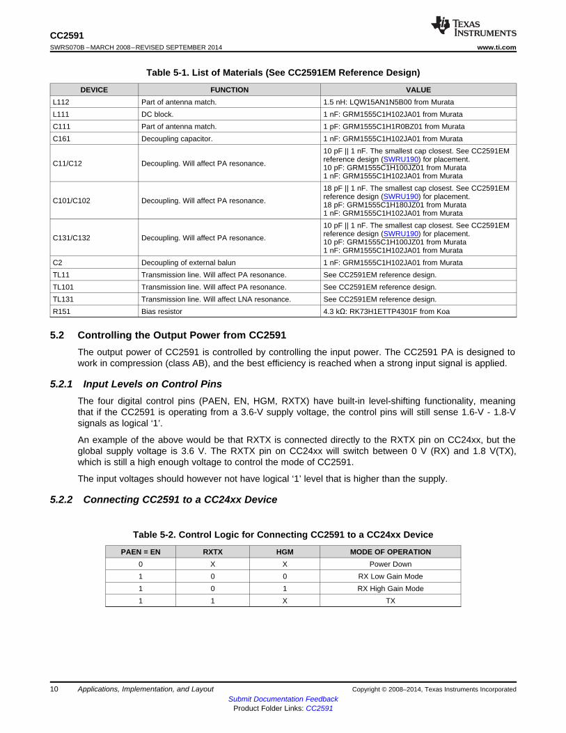
5.2.2 Connecting CC2591 to a CC24xx Device
Table 5-2. Control Logic for Connecting CC2591 to a CC24xx Device
PAEN = EN RXTX HGM MODE OF OPERATION0 X X Power Down1 0 0 RX Low Gain Mode1 0 1 RX High Gain Mode1 1 X TX
10 Applications, Implementation, and Layout Copyright © 2008–2014, Texas Instruments IncorporatedSubmit Documentation Feedback
Product Folder Links: CC2591
RF_P
RXTX
RF_N
RF_P
TXRX_SWITCH
RF_N
CC243x
RREG_OUT (CC243x)
Connected to
VDD/GND/MCU/RXTX
Alternativiely
from MCU
RF_P
RXTX
RF_N
= TLINE inductor
CC2591ANT
PAEN
EN
HGM
BIA
S
VDD
AV
DD
_P
A2
AV
DD
_P
A1
AV
DD
_LN
A
AV
DD
_B
IAS
VDD VDD
VDD
RF_P
RXTX
RF_N
L112 C113 C111
L111C112
C161
C11/C12 C101/C102
C131/C132
R151
TL
11
TL
10
1
TL
13
1
CC2591www.ti.com SWRS070B –MARCH 2008–REVISED SEPTEMBER 2014
Figure 5-2. CC2591 + CC24xx Application Circuit
Copyright © 2008–2014, Texas Instruments Incorporated Applications, Implementation, and Layout 11Submit Documentation Feedback
Product Folder Links: CC2591

RF_P
RXTX
RF_N
RF_P
RF_N
CC2500
CC2510
CC2511
Connected to
VDD/GND/MCU
Alternatively
from MCU
RF_P
RXTX
RF_N
= TLINE inductor
CC2591ANT
PAEN
EN
HGM
BIA
S
VDDA
VD
D_P
A2
AV
DD
_P
A1
AV
DD
_LN
A
AV
DD
_B
IAS
VDD VDD
VDD
RF_P
RXTX
RF_N
R151
TL
11
TL
10
1
TL
13
1
NC
GDO0
GDO2
L112 C113 C111
L111C112
C161
C11/C12 C101/C102
C131/C132
CC2591SWRS070B –MARCH 2008–REVISED SEPTEMBER 2014 www.ti.com
5.2.3 Connecting CC2591 to the CC2500, CC2510, or CC2511 Device
Table 5-3. Control Logic for Connecting CC2591 to a CC2500/10/11 Devices
PAEN EN RXTX HGM MODE OF OPERATION0 0 NC X Power Down0 1 NC 0 RX LGM0 1 NC 1 RX HGM1 0 NC X TX1 1 NC X Not allowed
Figure 5-3. CC2591 + CC2500/10/11 Device Application Circuit
12 Applications, Implementation, and Layout Copyright © 2008–2014, Texas Instruments IncorporatedSubmit Documentation Feedback
Product Folder Links: CC2591

RF_P
RXTX
RF_N
RF_P
RF_N
CC2520
Connected to
VDD/GND/MCU
Alternatively
from MCU
RF_P
RXTX
RF_N
= TLINE inductor
CC2591ANT
PAEN
EN
HGM
BIA
S
VDD
AV
DD
_P
A2
AV
DD
_P
A1
AV
DD
_LN
A
AV
DD
_B
IAS
VDD VDD
VDD
RF_P
RXTX
RF_N
R151
TL
11
TL
10
1
TL
13
1
NC
PA_EN
LNA_EN
C41
C21
L21
L41
C1
L112 C113 C111
L111C112
C161
C11/C12 C101/C102
C131/C132
CC2591www.ti.com SWRS070B –MARCH 2008–REVISED SEPTEMBER 2014
5.2.4 Connecting CC2591 to a CC2520 Device
Table 5-4. Control Logic for Connecting CC2591 to a CC2520 Device
PAEN EN RXTX HGM MODE OF OPERATION0 0 NC X Power Down0 1 NC 0 RX LGM0 1 NC 1 RX HGM1 0 NC X TX1 1 NC X Not allowed
Figure 5-4. CC2591 + CC2520 Application Circuit
Copyright © 2008–2014, Texas Instruments Incorporated Applications, Implementation, and Layout 13Submit Documentation Feedback
Product Folder Links: CC2591

CC2591SWRS070B –MARCH 2008–REVISED SEPTEMBER 2014 www.ti.com
6 Device and Documentation Support
6.1 Device Support
6.1.1 Development SupportTI offers an extensive line of development tools, including tools to evaluate the performance of theprocessors, generate code, develop algorithm implementations, and fully integrate and debug softwareand hardware modules. The tool's support documentation is electronically available within the CodeComposer Studio™ Integrated Development Environment (IDE).
The following products support development of the CC2591 device applications:
Software Development Tools: Code Composer Studio™ Integrated Development Environment (IDE):including Editor C/C++/Assembly Code Generation, and Debug plus additional development toolsScalable, Real-Time Foundation Software (DSP/BIOS™), which provides the basic run-time targetsoftware needed to support any CC2591 device application.
Hardware Development Tools: Extended Development System (XDS™) Emulator
For a complete listing of development-support tools for the CC2591 platform, visit the Texas Instrumentswebsite at www.ti.com. For information on pricing and availability, contact the nearest TI field sales officeor authorized distributor.
6.1.2 Device NomenclatureTo designate the stages in the product development cycle, TI assigns prefixes to the part numbers of allmicroprocessors (MPUs) and support tools. Each device has one of three prefixes: X, P, or null (no prefix)(for example, CC2591). These prefixes represent evolutionary stages of product development fromengineering prototypes (TMDX) through fully qualified production devices and tools (TMDS).
Device development evolutionary flow:
X Experimental device that is not necessarily representative of the final device's electricalspecifications and may not use production assembly flow.
P Prototype device that is not necessarily the final silicon die and may not necessarily meetfinal electrical specifications.
null Production version of the silicon die that is fully qualified.
Support tool development evolutionary flow:
X and P devices are shipped against the following disclaimer:
"Developmental product is intended for internal evaluation purposes."
Production devices have been characterized fully, and the quality and reliability of the device have beendemonstrated fully. TI's standard warranty applies.
Predictions show that prototype devices (X or P) have a greater failure rate than the standard productiondevices. Texas Instruments recommends that these devices not be used in any production systembecause their expected end-use failure rate still is undefined. Only qualified production devices are to beused.
TI device nomenclature also includes a suffix with the device family name. This suffix indicates thepackage type (for example, RGV) and the temperature range (for example, blank is the defaultcommercial temperature range). provides a legend for reading the complete device name for any CC2591device.
For orderable part numbers of CC2591 devices in the RGV package types, see the Package OptionAddendum of this document, the TI website (www.ti.com), or contact your TI sales representative.
14 Device and Documentation Support Copyright © 2008–2014, Texas Instruments IncorporatedSubmit Documentation Feedback
Product Folder Links: CC2591

CC2591www.ti.com SWRS070B –MARCH 2008–REVISED SEPTEMBER 2014
6.2 Documentation SupportThe following documents describe the CC2591 processor. Copies of these documents are available on theInternet at www.ti.com.
SWRA351 Antenna Quick Guide
SWRA120 Design Note Overview
SWRA350 YAGI 2.4 GHz PCB Antenna
SWRA161 Antenna Selection Guide
SWRA328 CC-Antenna-DK Documentation and Antenna Measurements Summary
SWRA229 Using CC2591 RF Front End with CC2520
SWRA308 Using CC2591 Front End with CC2530 and CC2531
SWRA290 TIMAC and Z-Stack Modifications for using CC2591 RF Front End with CC2
SWRA236 Design Steps and Results for Changing PCB Layer Thickness
SWRA230 TI-MAC modifications for using CC2591 PA/LNA with MSP430F2618+CC2520
SWRA208 TI-MAC and Z-Stack modifications for using CC2591 RF Front End w/CC2430
SWRA212 Using CC2591 RF Front End with CC2430
SWRC171 CC2530-CC2591EM Reference Design
SPRU137 CC2520 Software Examples User's Guide
SPRU178 CC2430 Software Examples User’s Guide
6.2.1 Community ResourcesThe following links connect to TI community resources. Linked contents are provided "AS IS" by therespective contributors. They do not constitute TI specifications and do not necessarily reflect TI's views;see TI's Terms of Use.
TI E2E™ Online Community TI's Engineer-to-Engineer (E2E) Community. Created to fostercollaboration among engineers. At e2e.ti.com, you can ask questions, share knowledge,explore ideas and help solve problems with fellow engineers.
TI Embedded Processors Wiki Texas Instruments Embedded Processors Wiki. Established to helpdevelopers get started with Embedded Processors from Texas Instruments and to fosterinnovation and growth of general knowledge about the hardware and software surroundingthese devices.
6.3 TrademarksE2E is a trademark of Texas Instruments.ZigBee is a registered trademark of ZigBee Alliance.
Copyright © 2008–2014, Texas Instruments Incorporated Device and Documentation Support 15Submit Documentation Feedback
Product Folder Links: CC2591

CC2591SWRS070B –MARCH 2008–REVISED SEPTEMBER 2014 www.ti.com
6.4 Electrostatic Discharge CautionThis integrated circuit can be damaged by ESD. Texas Instruments recommends that all integrated circuits be handled withappropriate precautions. Failure to observe proper handling and installation procedures can cause damage.
ESD damage can range from subtle performance degradation to complete device failure. Precision integrated circuits may be moresusceptible to damage because very small parametric changes could cause the device not to meet its published specifications.
6.5 Export Control NoticeRecipient agrees to not knowingly export or re-export, directly or indirectly, any product or technical data(as defined by the U.S., EU, and other Export Administration Regulations) including software, or anycontrolled product restricted by other applicable national regulations, received from disclosing party undernondisclosure obligations (if any), or any direct product of such technology, to any destination to whichsuch export or re-export is restricted or prohibited by U.S. or other applicable laws, without obtaining priorauthorization from U.S. Department of Commerce and other competent Government authorities to theextent required by those laws.
6.6 GlossarySLYZ022 — TI Glossary.
This glossary lists and explains terms, acronyms, and definitions.
16 Device and Documentation Support Copyright © 2008–2014, Texas Instruments IncorporatedSubmit Documentation Feedback
Product Folder Links: CC2591

CC2591www.ti.com SWRS070B –MARCH 2008–REVISED SEPTEMBER 2014
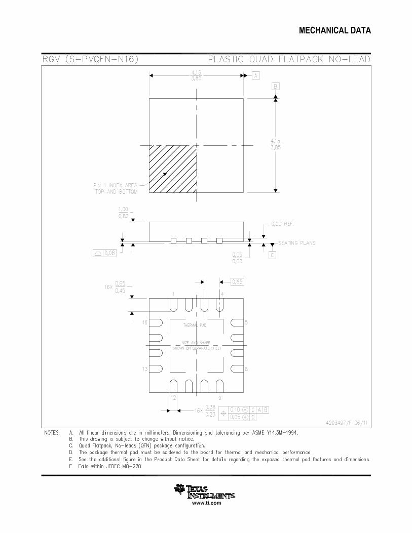
7 Mechanical Packaging and Orderable Information
7.1 Packaging InformationThe following pages include mechanical packaging and orderable information. This information is the mostcurrent data available for the designated devices. This data is subject to change without notice andrevision of this document. For browser-based versions of this data sheet, refer to the left-hand navigation.
Copyright © 2008–2014, Texas Instruments Incorporated Mechanical Packaging and Orderable Information 17Submit Documentation Feedback
Product Folder Links: CC2591
PACKAGE OPTION ADDENDUM
www.ti.com 24-Aug-2018
Addendum-Page 1
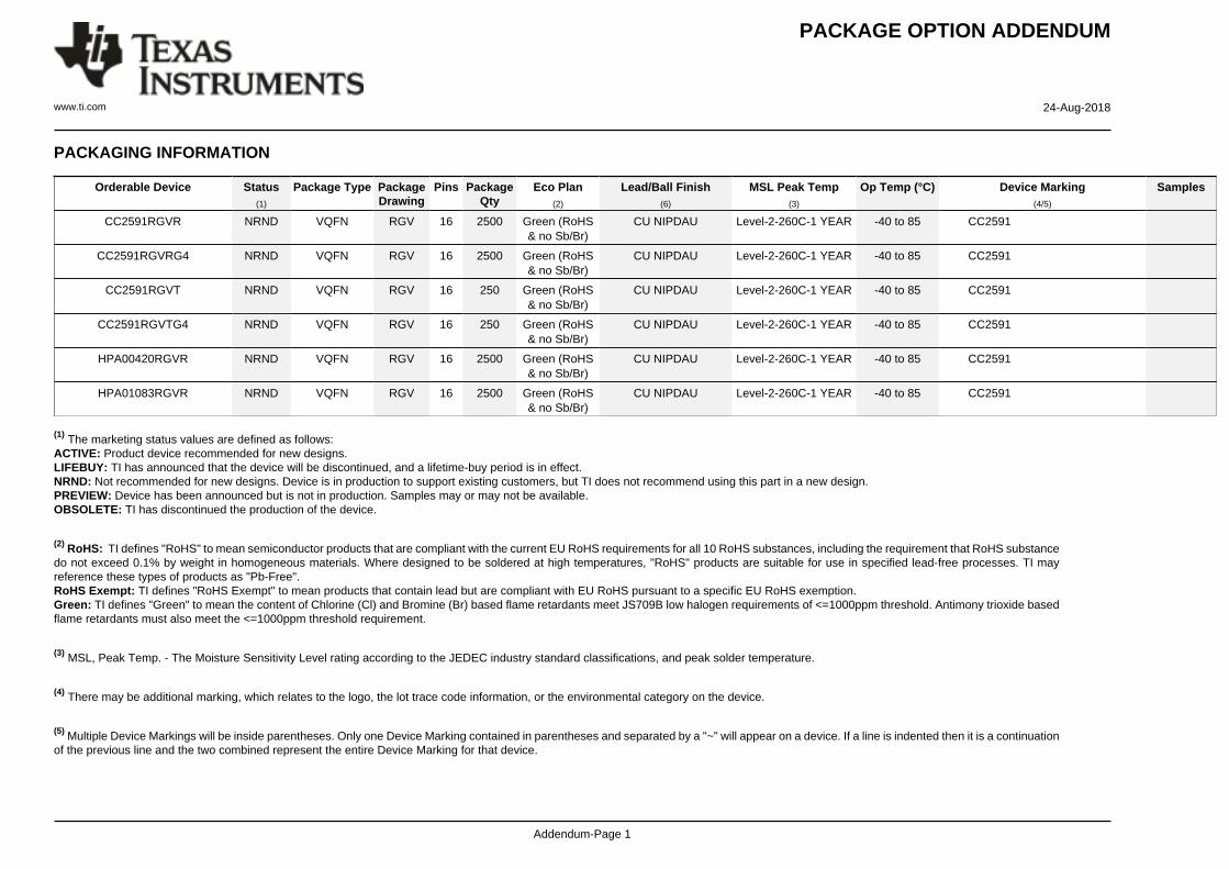
PACKAGING INFORMATION
Orderable Device Status(1)
Package Type PackageDrawing
Pins PackageQty
Eco Plan(2)
Lead/Ball Finish(6)
MSL Peak Temp(3)
Op Temp (°C) Device Marking(4/5)
Samples
CC2591RGVR NRND VQFN RGV 16 2500 Green (RoHS& no Sb/Br)
CU NIPDAU Level-2-260C-1 YEAR -40 to 85 CC2591
CC2591RGVRG4 NRND VQFN RGV 16 2500 Green (RoHS& no Sb/Br)
CU NIPDAU Level-2-260C-1 YEAR -40 to 85 CC2591
CC2591RGVT NRND VQFN RGV 16 250 Green (RoHS& no Sb/Br)
CU NIPDAU Level-2-260C-1 YEAR -40 to 85 CC2591
CC2591RGVTG4 NRND VQFN RGV 16 250 Green (RoHS& no Sb/Br)
CU NIPDAU Level-2-260C-1 YEAR -40 to 85 CC2591
HPA00420RGVR NRND VQFN RGV 16 2500 Green (RoHS& no Sb/Br)
CU NIPDAU Level-2-260C-1 YEAR -40 to 85 CC2591
HPA01083RGVR NRND VQFN RGV 16 2500 Green (RoHS& no Sb/Br)
CU NIPDAU Level-2-260C-1 YEAR -40 to 85 CC2591
(1) The marketing status values are defined as follows:ACTIVE: Product device recommended for new designs.LIFEBUY: TI has announced that the device will be discontinued, and a lifetime-buy period is in effect.NRND: Not recommended for new designs. Device is in production to support existing customers, but TI does not recommend using this part in a new design.PREVIEW: Device has been announced but is not in production. Samples may or may not be available.OBSOLETE: TI has discontinued the production of the device.
(2) RoHS: TI defines "RoHS" to mean semiconductor products that are compliant with the current EU RoHS requirements for all 10 RoHS substances, including the requirement that RoHS substancedo not exceed 0.1% by weight in homogeneous materials. Where designed to be soldered at high temperatures, "RoHS" products are suitable for use in specified lead-free processes. TI mayreference these types of products as "Pb-Free".RoHS Exempt: TI defines "RoHS Exempt" to mean products that contain lead but are compliant with EU RoHS pursuant to a specific EU RoHS exemption.Green: TI defines "Green" to mean the content of Chlorine (Cl) and Bromine (Br) based flame retardants meet JS709B low halogen requirements of <=1000ppm threshold. Antimony trioxide basedflame retardants must also meet the <=1000ppm threshold requirement.
(3) MSL, Peak Temp. - The Moisture Sensitivity Level rating according to the JEDEC industry standard classifications, and peak solder temperature.
(4) There may be additional marking, which relates to the logo, the lot trace code information, or the environmental category on the device.
(5) Multiple Device Markings will be inside parentheses. Only one Device Marking contained in parentheses and separated by a "~" will appear on a device. If a line is indented then it is a continuationof the previous line and the two combined represent the entire Device Marking for that device.

PACKAGE OPTION ADDENDUM
www.ti.com 24-Aug-2018
Addendum-Page 2
(6) Lead/Ball Finish - Orderable Devices may have multiple material finish options. Finish options are separated by a vertical ruled line. Lead/Ball Finish values may wrap to two lines if the finishvalue exceeds the maximum column width.
Important Information and Disclaimer:The information provided on this page represents TI's knowledge and belief as of the date that it is provided. TI bases its knowledge and belief on informationprovided by third parties, and makes no representation or warranty as to the accuracy of such information. Efforts are underway to better integrate information from third parties. TI has taken andcontinues to take reasonable steps to provide representative and accurate information but may not have conducted destructive testing or chemical analysis on incoming materials and chemicals.TI and TI suppliers consider certain information to be proprietary, and thus CAS numbers and other limited information may not be available for release.
In no event shall TI's liability arising out of such information exceed the total purchase price of the TI part(s) at issue in this document sold by TI to Customer on an annual basis.

TAPE AND REEL INFORMATION
*All dimensions are nominal
Device PackageType
PackageDrawing
Pins SPQ ReelDiameter
(mm)
ReelWidth
W1 (mm)
A0(mm)
B0(mm)
K0(mm)
P1(mm)
W(mm)
Pin1Quadrant
CC2591RGVR VQFN RGV 16 2500 330.0 12.4 4.3 4.3 1.5 8.0 12.0 Q2
CC2591RGVT VQFN RGV 16 250 180.0 12.4 4.3 4.3 1.5 8.0 12.0 Q2
PACKAGE MATERIALS INFORMATION
www.ti.com 3-Aug-2017
Pack Materials-Page 1

*All dimensions are nominal
Device Package Type Package Drawing Pins SPQ Length (mm) Width (mm) Height (mm)
CC2591RGVR VQFN RGV 16 2500 336.6 336.6 28.6
CC2591RGVT VQFN RGV 16 250 210.0 185.0 35.0
PACKAGE MATERIALS INFORMATION
www.ti.com 3-Aug-2017
Pack Materials-Page 2


IMPORTANT NOTICE
Texas Instruments Incorporated (TI) reserves the right to make corrections, enhancements, improvements and other changes to itssemiconductor products and services per JESD46, latest issue, and to discontinue any product or service per JESD48, latest issue. Buyersshould obtain the latest relevant information before placing orders and should verify that such information is current and complete.TI’s published terms of sale for semiconductor products (http://www.ti.com/sc/docs/stdterms.htm) apply to the sale of packaged integratedcircuit products that TI has qualified and released to market. Additional terms may apply to the use or sale of other types of TI products andservices.Reproduction of significant portions of TI information in TI data sheets is permissible only if reproduction is without alteration and isaccompanied by all associated warranties, conditions, limitations, and notices. TI is not responsible or liable for such reproduceddocumentation. Information of third parties may be subject to additional restrictions. Resale of TI products or services with statementsdifferent from or beyond the parameters stated by TI for that product or service voids all express and any implied warranties for theassociated TI product or service and is an unfair and deceptive business practice. TI is not responsible or liable for any such statements.Buyers and others who are developing systems that incorporate TI products (collectively, “Designers”) understand and agree that Designersremain responsible for using their independent analysis, evaluation and judgment in designing their applications and that Designers havefull and exclusive responsibility to assure the safety of Designers' applications and compliance of their applications (and of all TI productsused in or for Designers’ applications) with all applicable regulations, laws and other applicable requirements. Designer represents that, withrespect to their applications, Designer has all the necessary expertise to create and implement safeguards that (1) anticipate dangerousconsequences of failures, (2) monitor failures and their consequences, and (3) lessen the likelihood of failures that might cause harm andtake appropriate actions. Designer agrees that prior to using or distributing any applications that include TI products, Designer willthoroughly test such applications and the functionality of such TI products as used in such applications.TI’s provision of technical, application or other design advice, quality characterization, reliability data or other services or information,including, but not limited to, reference designs and materials relating to evaluation modules, (collectively, “TI Resources”) are intended toassist designers who are developing applications that incorporate TI products; by downloading, accessing or using TI Resources in anyway, Designer (individually or, if Designer is acting on behalf of a company, Designer’s company) agrees to use any particular TI Resourcesolely for this purpose and subject to the terms of this Notice.TI’s provision of TI Resources does not expand or otherwise alter TI’s applicable published warranties or warranty disclaimers for TIproducts, and no additional obligations or liabilities arise from TI providing such TI Resources. TI reserves the right to make corrections,enhancements, improvements and other changes to its TI Resources. TI has not conducted any testing other than that specificallydescribed in the published documentation for a particular TI Resource.Designer is authorized to use, copy and modify any individual TI Resource only in connection with the development of applications thatinclude the TI product(s) identified in such TI Resource. NO OTHER LICENSE, EXPRESS OR IMPLIED, BY ESTOPPEL OR OTHERWISETO ANY OTHER TI INTELLECTUAL PROPERTY RIGHT, AND NO LICENSE TO ANY TECHNOLOGY OR INTELLECTUAL PROPERTYRIGHT OF TI OR ANY THIRD PARTY IS GRANTED HEREIN, including but not limited to any patent right, copyright, mask work right, orother intellectual property right relating to any combination, machine, or process in which TI products or services are used. Informationregarding or referencing third-party products or services does not constitute a license to use such products or services, or a warranty orendorsement thereof. Use of TI Resources may require a license from a third party under the patents or other intellectual property of thethird party, or a license from TI under the patents or other intellectual property of TI.TI RESOURCES ARE PROVIDED “AS IS” AND WITH ALL FAULTS. TI DISCLAIMS ALL OTHER WARRANTIES ORREPRESENTATIONS, EXPRESS OR IMPLIED, REGARDING RESOURCES OR USE THEREOF, INCLUDING BUT NOT LIMITED TOACCURACY OR COMPLETENESS, TITLE, ANY EPIDEMIC FAILURE WARRANTY AND ANY IMPLIED WARRANTIES OFMERCHANTABILITY, FITNESS FOR A PARTICULAR PURPOSE, AND NON-INFRINGEMENT OF ANY THIRD PARTY INTELLECTUALPROPERTY RIGHTS. TI SHALL NOT BE LIABLE FOR AND SHALL NOT DEFEND OR INDEMNIFY DESIGNER AGAINST ANY CLAIM,INCLUDING BUT NOT LIMITED TO ANY INFRINGEMENT CLAIM THAT RELATES TO OR IS BASED ON ANY COMBINATION OFPRODUCTS EVEN IF DESCRIBED IN TI RESOURCES OR OTHERWISE. IN NO EVENT SHALL TI BE LIABLE FOR ANY ACTUAL,DIRECT, SPECIAL, COLLATERAL, INDIRECT, PUNITIVE, INCIDENTAL, CONSEQUENTIAL OR EXEMPLARY DAMAGES INCONNECTION WITH OR ARISING OUT OF TI RESOURCES OR USE THEREOF, AND REGARDLESS OF WHETHER TI HAS BEENADVISED OF THE POSSIBILITY OF SUCH DAMAGES.Unless TI has explicitly designated an individual product as meeting the requirements of a particular industry standard (e.g., ISO/TS 16949and ISO 26262), TI is not responsible for any failure to meet such industry standard requirements.Where TI specifically promotes products as facilitating functional safety or as compliant with industry functional safety standards, suchproducts are intended to help enable customers to design and create their own applications that meet applicable functional safety standardsand requirements. Using products in an application does not by itself establish any safety features in the application. Designers mustensure compliance with safety-related requirements and standards applicable to their applications. Designer may not use any TI products inlife-critical medical equipment unless authorized officers of the parties have executed a special contract specifically governing such use.Life-critical medical equipment is medical equipment where failure of such equipment would cause serious bodily injury or death (e.g., lifesupport, pacemakers, defibrillators, heart pumps, neurostimulators, and implantables). Such equipment includes, without limitation, allmedical devices identified by the U.S. Food and Drug Administration as Class III devices and equivalent classifications outside the U.S.TI may expressly designate certain products as completing a particular qualification (e.g., Q100, Military Grade, or Enhanced Product).Designers agree that it has the necessary expertise to select the product with the appropriate qualification designation for their applicationsand that proper product selection is at Designers’ own risk. Designers are solely responsible for compliance with all legal and regulatoryrequirements in connection with such selection.Designer will fully indemnify TI and its representatives against any damages, costs, losses, and/or liabilities arising out of Designer’s non-compliance with the terms and provisions of this Notice.
Mailing Address: Texas Instruments, Post Office Box 655303, Dallas, Texas 75265Copyright © 2018, Texas Instruments Incorporated